WO2021210047A1 - Method for manufacturing semiconductor element - Google Patents
Method for manufacturing semiconductor element Download PDFInfo
- Publication number
- WO2021210047A1 WO2021210047A1 PCT/JP2020/016312 JP2020016312W WO2021210047A1 WO 2021210047 A1 WO2021210047 A1 WO 2021210047A1 JP 2020016312 W JP2020016312 W JP 2020016312W WO 2021210047 A1 WO2021210047 A1 WO 2021210047A1
- Authority
- WO
- WIPO (PCT)
- Prior art keywords
- substrate
- circuit element
- semiconductor
- manufacturing
- support substrate
- Prior art date
Links
- 239000004065 semiconductor Substances 0.000 title claims abstract description 98
- 238000000034 method Methods 0.000 title claims abstract description 50
- 238000004519 manufacturing process Methods 0.000 title claims abstract description 37
- 239000000758 substrate Substances 0.000 claims abstract description 227
- 229910052751 metal Inorganic materials 0.000 claims abstract description 29
- 239000002184 metal Substances 0.000 claims abstract description 29
- 239000010409 thin film Substances 0.000 claims abstract description 25
- 238000009792 diffusion process Methods 0.000 claims abstract description 10
- 239000010408 film Substances 0.000 claims description 47
- 239000010410 layer Substances 0.000 claims description 37
- 239000011241 protective layer Substances 0.000 claims description 34
- 239000000463 material Substances 0.000 claims description 15
- 229910003460 diamond Inorganic materials 0.000 claims description 6
- 239000010432 diamond Substances 0.000 claims description 6
- 238000005304 joining Methods 0.000 claims description 5
- OKTJSMMVPCPJKN-UHFFFAOYSA-N Carbon Chemical compound [C] OKTJSMMVPCPJKN-UHFFFAOYSA-N 0.000 claims description 4
- 229910052799 carbon Inorganic materials 0.000 claims description 4
- 230000001678 irradiating effect Effects 0.000 claims description 4
- 239000004925 Acrylic resin Substances 0.000 claims description 3
- 229920000178 Acrylic resin Polymers 0.000 claims description 3
- JMASRVWKEDWRBT-UHFFFAOYSA-N Gallium nitride Chemical compound [Ga]#N JMASRVWKEDWRBT-UHFFFAOYSA-N 0.000 claims description 3
- 230000015572 biosynthetic process Effects 0.000 claims description 3
- 239000011810 insulating material Substances 0.000 claims description 3
- FRWYFWZENXDZMU-UHFFFAOYSA-N 2-iodoquinoline Chemical compound C1=CC=CC2=NC(I)=CC=C21 FRWYFWZENXDZMU-UHFFFAOYSA-N 0.000 claims description 2
- 229910002601 GaN Inorganic materials 0.000 claims description 2
- 229910052581 Si3N4 Inorganic materials 0.000 claims description 2
- LTPBRCUWZOMYOC-UHFFFAOYSA-N beryllium oxide Inorganic materials O=[Be] LTPBRCUWZOMYOC-UHFFFAOYSA-N 0.000 claims description 2
- PMHQVHHXPFUNSP-UHFFFAOYSA-M copper(1+);methylsulfanylmethane;bromide Chemical compound Br[Cu].CSC PMHQVHHXPFUNSP-UHFFFAOYSA-M 0.000 claims description 2
- 239000003822 epoxy resin Substances 0.000 claims description 2
- 229920000647 polyepoxide Polymers 0.000 claims description 2
- HQVNEWCFYHHQES-UHFFFAOYSA-N silicon nitride Chemical compound N12[Si]34N5[Si]62N3[Si]51N64 HQVNEWCFYHHQES-UHFFFAOYSA-N 0.000 claims description 2
- 230000007547 defect Effects 0.000 abstract description 9
- 238000005498 polishing Methods 0.000 description 23
- 239000011347 resin Substances 0.000 description 14
- 229920005989 resin Polymers 0.000 description 14
- 235000012431 wafers Nutrition 0.000 description 9
- 239000000853 adhesive Substances 0.000 description 6
- 230000001070 adhesive effect Effects 0.000 description 6
- ORQBXQOJMQIAOY-UHFFFAOYSA-N nobelium Chemical compound [No] ORQBXQOJMQIAOY-UHFFFAOYSA-N 0.000 description 6
- 239000000126 substance Substances 0.000 description 6
- 238000005530 etching Methods 0.000 description 5
- 230000000694 effects Effects 0.000 description 4
- 230000017525 heat dissipation Effects 0.000 description 4
- 238000004528 spin coating Methods 0.000 description 3
- 229920001187 thermosetting polymer Polymers 0.000 description 3
- XEEYBQQBJWHFJM-UHFFFAOYSA-N Iron Chemical compound [Fe] XEEYBQQBJWHFJM-UHFFFAOYSA-N 0.000 description 2
- XUIMIQQOPSSXEZ-UHFFFAOYSA-N Silicon Chemical compound [Si] XUIMIQQOPSSXEZ-UHFFFAOYSA-N 0.000 description 2
- 230000002378 acidificating effect Effects 0.000 description 2
- 230000004913 activation Effects 0.000 description 2
- 238000004380 ashing Methods 0.000 description 2
- QVGXLLKOCUKJST-UHFFFAOYSA-N atomic oxygen Chemical compound [O] QVGXLLKOCUKJST-UHFFFAOYSA-N 0.000 description 2
- 238000000576 coating method Methods 0.000 description 2
- 238000007796 conventional method Methods 0.000 description 2
- 238000005336 cracking Methods 0.000 description 2
- 230000007423 decrease Effects 0.000 description 2
- 239000011521 glass Substances 0.000 description 2
- 238000010438 heat treatment Methods 0.000 description 2
- 230000007935 neutral effect Effects 0.000 description 2
- 239000003960 organic solvent Substances 0.000 description 2
- 229910052760 oxygen Inorganic materials 0.000 description 2
- 239000001301 oxygen Substances 0.000 description 2
- 230000002093 peripheral effect Effects 0.000 description 2
- 238000001020 plasma etching Methods 0.000 description 2
- 229920013716 polyethylene resin Polymers 0.000 description 2
- 229910052710 silicon Inorganic materials 0.000 description 2
- 239000010703 silicon Substances 0.000 description 2
- HBMJWWWQQXIZIP-UHFFFAOYSA-N silicon carbide Chemical compound [Si+]#[C-] HBMJWWWQQXIZIP-UHFFFAOYSA-N 0.000 description 2
- 229910010271 silicon carbide Inorganic materials 0.000 description 2
- 238000004544 sputter deposition Methods 0.000 description 2
- 238000005477 sputtering target Methods 0.000 description 2
- VYZAMTAEIAYCRO-UHFFFAOYSA-N Chromium Chemical compound [Cr] VYZAMTAEIAYCRO-UHFFFAOYSA-N 0.000 description 1
- RYGMFSIKBFXOCR-UHFFFAOYSA-N Copper Chemical compound [Cu] RYGMFSIKBFXOCR-UHFFFAOYSA-N 0.000 description 1
- 239000004743 Polypropylene Substances 0.000 description 1
- VYPSYNLAJGMNEJ-UHFFFAOYSA-N Silicium dioxide Chemical compound O=[Si]=O VYPSYNLAJGMNEJ-UHFFFAOYSA-N 0.000 description 1
- BQCADISMDOOEFD-UHFFFAOYSA-N Silver Chemical compound [Ag] BQCADISMDOOEFD-UHFFFAOYSA-N 0.000 description 1
- RTAQQCXQSZGOHL-UHFFFAOYSA-N Titanium Chemical compound [Ti] RTAQQCXQSZGOHL-UHFFFAOYSA-N 0.000 description 1
- 239000012790 adhesive layer Substances 0.000 description 1
- 230000002411 adverse Effects 0.000 description 1
- 239000003513 alkali Substances 0.000 description 1
- 229910052782 aluminium Inorganic materials 0.000 description 1
- XAGFODPZIPBFFR-UHFFFAOYSA-N aluminium Chemical compound [Al] XAGFODPZIPBFFR-UHFFFAOYSA-N 0.000 description 1
- 239000003575 carbonaceous material Substances 0.000 description 1
- 238000005229 chemical vapour deposition Methods 0.000 description 1
- 229910052804 chromium Inorganic materials 0.000 description 1
- 239000011651 chromium Substances 0.000 description 1
- 238000004140 cleaning Methods 0.000 description 1
- 239000011248 coating agent Substances 0.000 description 1
- 229910052802 copper Inorganic materials 0.000 description 1
- 239000010949 copper Substances 0.000 description 1
- 238000001312 dry etching Methods 0.000 description 1
- 238000001035 drying Methods 0.000 description 1
- 230000005669 field effect Effects 0.000 description 1
- PCHJSUWPFVWCPO-UHFFFAOYSA-N gold Chemical compound [Au] PCHJSUWPFVWCPO-UHFFFAOYSA-N 0.000 description 1
- 229910052737 gold Inorganic materials 0.000 description 1
- 239000010931 gold Substances 0.000 description 1
- 238000007654 immersion Methods 0.000 description 1
- 238000010884 ion-beam technique Methods 0.000 description 1
- 229910052742 iron Inorganic materials 0.000 description 1
- 239000007788 liquid Substances 0.000 description 1
- 239000005416 organic matter Substances 0.000 description 1
- 239000005011 phenolic resin Substances 0.000 description 1
- 229920002120 photoresistant polymer Polymers 0.000 description 1
- 238000007517 polishing process Methods 0.000 description 1
- 229920005672 polyolefin resin Polymers 0.000 description 1
- -1 polypropylene Polymers 0.000 description 1
- 229920001155 polypropylene Polymers 0.000 description 1
- 229910052594 sapphire Inorganic materials 0.000 description 1
- 239000010980 sapphire Substances 0.000 description 1
- 229910052814 silicon oxide Inorganic materials 0.000 description 1
- 229910052709 silver Inorganic materials 0.000 description 1
- 239000004332 silver Substances 0.000 description 1
- 239000002904 solvent Substances 0.000 description 1
- 238000005507 spraying Methods 0.000 description 1
- 229910052719 titanium Inorganic materials 0.000 description 1
- 239000010936 titanium Substances 0.000 description 1
- 238000002834 transmittance Methods 0.000 description 1
- 238000007740 vapor deposition Methods 0.000 description 1
Images


Classifications
-
- H—ELECTRICITY
- H01—ELECTRIC ELEMENTS
- H01L—SEMICONDUCTOR DEVICES NOT COVERED BY CLASS H10
- H01L21/00—Processes or apparatus adapted for the manufacture or treatment of semiconductor or solid state devices or of parts thereof
- H01L21/02—Manufacture or treatment of semiconductor devices or of parts thereof
- H01L21/04—Manufacture or treatment of semiconductor devices or of parts thereof the devices having at least one potential-jump barrier or surface barrier, e.g. PN junction, depletion layer or carrier concentration layer
- H01L21/18—Manufacture or treatment of semiconductor devices or of parts thereof the devices having at least one potential-jump barrier or surface barrier, e.g. PN junction, depletion layer or carrier concentration layer the devices having semiconductor bodies comprising elements of Group IV of the Periodic System or AIIIBV compounds with or without impurities, e.g. doping materials
- H01L21/185—Joining of semiconductor bodies for junction formation
-
- H—ELECTRICITY
- H01—ELECTRIC ELEMENTS
- H01L—SEMICONDUCTOR DEVICES NOT COVERED BY CLASS H10
- H01L21/00—Processes or apparatus adapted for the manufacture or treatment of semiconductor or solid state devices or of parts thereof
- H01L21/02—Manufacture or treatment of semiconductor devices or of parts thereof
- H01L21/04—Manufacture or treatment of semiconductor devices or of parts thereof the devices having at least one potential-jump barrier or surface barrier, e.g. PN junction, depletion layer or carrier concentration layer
- H01L21/18—Manufacture or treatment of semiconductor devices or of parts thereof the devices having at least one potential-jump barrier or surface barrier, e.g. PN junction, depletion layer or carrier concentration layer the devices having semiconductor bodies comprising elements of Group IV of the Periodic System or AIIIBV compounds with or without impurities, e.g. doping materials
- H01L21/30—Treatment of semiconductor bodies using processes or apparatus not provided for in groups H01L21/20 - H01L21/26
- H01L21/302—Treatment of semiconductor bodies using processes or apparatus not provided for in groups H01L21/20 - H01L21/26 to change their surface-physical characteristics or shape, e.g. etching, polishing, cutting
- H01L21/304—Mechanical treatment, e.g. grinding, polishing, cutting
-
- H—ELECTRICITY
- H01—ELECTRIC ELEMENTS
- H01L—SEMICONDUCTOR DEVICES NOT COVERED BY CLASS H10
- H01L21/00—Processes or apparatus adapted for the manufacture or treatment of semiconductor or solid state devices or of parts thereof
- H01L21/67—Apparatus specially adapted for handling semiconductor or electric solid state devices during manufacture or treatment thereof; Apparatus specially adapted for handling wafers during manufacture or treatment of semiconductor or electric solid state devices or components ; Apparatus not specifically provided for elsewhere
- H01L21/683—Apparatus specially adapted for handling semiconductor or electric solid state devices during manufacture or treatment thereof; Apparatus specially adapted for handling wafers during manufacture or treatment of semiconductor or electric solid state devices or components ; Apparatus not specifically provided for elsewhere for supporting or gripping
- H01L21/6835—Apparatus specially adapted for handling semiconductor or electric solid state devices during manufacture or treatment thereof; Apparatus specially adapted for handling wafers during manufacture or treatment of semiconductor or electric solid state devices or components ; Apparatus not specifically provided for elsewhere for supporting or gripping using temporarily an auxiliary support
-
- H—ELECTRICITY
- H01—ELECTRIC ELEMENTS
- H01L—SEMICONDUCTOR DEVICES NOT COVERED BY CLASS H10
- H01L21/00—Processes or apparatus adapted for the manufacture or treatment of semiconductor or solid state devices or of parts thereof
- H01L21/70—Manufacture or treatment of devices consisting of a plurality of solid state components formed in or on a common substrate or of parts thereof; Manufacture of integrated circuit devices or of parts thereof
- H01L21/77—Manufacture or treatment of devices consisting of a plurality of solid state components or integrated circuits formed in, or on, a common substrate
- H01L21/78—Manufacture or treatment of devices consisting of a plurality of solid state components or integrated circuits formed in, or on, a common substrate with subsequent division of the substrate into plural individual devices
-
- H—ELECTRICITY
- H01—ELECTRIC ELEMENTS
- H01L—SEMICONDUCTOR DEVICES NOT COVERED BY CLASS H10
- H01L29/00—Semiconductor devices adapted for rectifying, amplifying, oscillating or switching, or capacitors or resistors with at least one potential-jump barrier or surface barrier, e.g. PN junction depletion layer or carrier concentration layer; Details of semiconductor bodies or of electrodes thereof ; Multistep manufacturing processes therefor
- H01L29/02—Semiconductor bodies ; Multistep manufacturing processes therefor
- H01L29/12—Semiconductor bodies ; Multistep manufacturing processes therefor characterised by the materials of which they are formed
- H01L29/20—Semiconductor bodies ; Multistep manufacturing processes therefor characterised by the materials of which they are formed including, apart from doping materials or other impurities, only AIIIBV compounds
- H01L29/2003—Nitride compounds
-
- H—ELECTRICITY
- H01—ELECTRIC ELEMENTS
- H01L—SEMICONDUCTOR DEVICES NOT COVERED BY CLASS H10
- H01L29/00—Semiconductor devices adapted for rectifying, amplifying, oscillating or switching, or capacitors or resistors with at least one potential-jump barrier or surface barrier, e.g. PN junction depletion layer or carrier concentration layer; Details of semiconductor bodies or of electrodes thereof ; Multistep manufacturing processes therefor
- H01L29/66—Types of semiconductor device ; Multistep manufacturing processes therefor
- H01L29/66007—Multistep manufacturing processes
- H01L29/66075—Multistep manufacturing processes of devices having semiconductor bodies comprising group 14 or group 13/15 materials
- H01L29/66227—Multistep manufacturing processes of devices having semiconductor bodies comprising group 14 or group 13/15 materials the devices being controllable only by the electric current supplied or the electric potential applied, to an electrode which does not carry the current to be rectified, amplified or switched, e.g. three-terminal devices
- H01L29/66409—Unipolar field-effect transistors
- H01L29/66446—Unipolar field-effect transistors with an active layer made of a group 13/15 material, e.g. group 13/15 velocity modulation transistor [VMT], group 13/15 negative resistance FET [NERFET]
- H01L29/66462—Unipolar field-effect transistors with an active layer made of a group 13/15 material, e.g. group 13/15 velocity modulation transistor [VMT], group 13/15 negative resistance FET [NERFET] with a heterojunction interface channel or gate, e.g. HFET, HIGFET, SISFET, HJFET, HEMT
-
- H—ELECTRICITY
- H01—ELECTRIC ELEMENTS
- H01L—SEMICONDUCTOR DEVICES NOT COVERED BY CLASS H10
- H01L2221/00—Processes or apparatus adapted for the manufacture or treatment of semiconductor or solid state devices or of parts thereof covered by H01L21/00
- H01L2221/67—Apparatus for handling semiconductor or electric solid state devices during manufacture or treatment thereof; Apparatus for handling wafers during manufacture or treatment of semiconductor or electric solid state devices or components; Apparatus not specifically provided for elsewhere
- H01L2221/683—Apparatus for handling semiconductor or electric solid state devices during manufacture or treatment thereof; Apparatus for handling wafers during manufacture or treatment of semiconductor or electric solid state devices or components; Apparatus not specifically provided for elsewhere for supporting or gripping
- H01L2221/68304—Apparatus for handling semiconductor or electric solid state devices during manufacture or treatment thereof; Apparatus for handling wafers during manufacture or treatment of semiconductor or electric solid state devices or components; Apparatus not specifically provided for elsewhere for supporting or gripping using temporarily an auxiliary support
- H01L2221/68318—Auxiliary support including means facilitating the separation of a device or wafer from the auxiliary support
-
- H—ELECTRICITY
- H01—ELECTRIC ELEMENTS
- H01L—SEMICONDUCTOR DEVICES NOT COVERED BY CLASS H10
- H01L2221/00—Processes or apparatus adapted for the manufacture or treatment of semiconductor or solid state devices or of parts thereof covered by H01L21/00
- H01L2221/67—Apparatus for handling semiconductor or electric solid state devices during manufacture or treatment thereof; Apparatus for handling wafers during manufacture or treatment of semiconductor or electric solid state devices or components; Apparatus not specifically provided for elsewhere
- H01L2221/683—Apparatus for handling semiconductor or electric solid state devices during manufacture or treatment thereof; Apparatus for handling wafers during manufacture or treatment of semiconductor or electric solid state devices or components; Apparatus not specifically provided for elsewhere for supporting or gripping
- H01L2221/68304—Apparatus for handling semiconductor or electric solid state devices during manufacture or treatment thereof; Apparatus for handling wafers during manufacture or treatment of semiconductor or electric solid state devices or components; Apparatus not specifically provided for elsewhere for supporting or gripping using temporarily an auxiliary support
- H01L2221/68327—Apparatus for handling semiconductor or electric solid state devices during manufacture or treatment thereof; Apparatus for handling wafers during manufacture or treatment of semiconductor or electric solid state devices or components; Apparatus not specifically provided for elsewhere for supporting or gripping using temporarily an auxiliary support used during dicing or grinding
-
- H—ELECTRICITY
- H01—ELECTRIC ELEMENTS
- H01L—SEMICONDUCTOR DEVICES NOT COVERED BY CLASS H10
- H01L2221/00—Processes or apparatus adapted for the manufacture or treatment of semiconductor or solid state devices or of parts thereof covered by H01L21/00
- H01L2221/67—Apparatus for handling semiconductor or electric solid state devices during manufacture or treatment thereof; Apparatus for handling wafers during manufacture or treatment of semiconductor or electric solid state devices or components; Apparatus not specifically provided for elsewhere
- H01L2221/683—Apparatus for handling semiconductor or electric solid state devices during manufacture or treatment thereof; Apparatus for handling wafers during manufacture or treatment of semiconductor or electric solid state devices or components; Apparatus not specifically provided for elsewhere for supporting or gripping
- H01L2221/68304—Apparatus for handling semiconductor or electric solid state devices during manufacture or treatment thereof; Apparatus for handling wafers during manufacture or treatment of semiconductor or electric solid state devices or components; Apparatus not specifically provided for elsewhere for supporting or gripping using temporarily an auxiliary support
- H01L2221/6834—Apparatus for handling semiconductor or electric solid state devices during manufacture or treatment thereof; Apparatus for handling wafers during manufacture or treatment of semiconductor or electric solid state devices or components; Apparatus not specifically provided for elsewhere for supporting or gripping using temporarily an auxiliary support used to protect an active side of a device or wafer
-
- H—ELECTRICITY
- H01—ELECTRIC ELEMENTS
- H01L—SEMICONDUCTOR DEVICES NOT COVERED BY CLASS H10
- H01L2221/00—Processes or apparatus adapted for the manufacture or treatment of semiconductor or solid state devices or of parts thereof covered by H01L21/00
- H01L2221/67—Apparatus for handling semiconductor or electric solid state devices during manufacture or treatment thereof; Apparatus for handling wafers during manufacture or treatment of semiconductor or electric solid state devices or components; Apparatus not specifically provided for elsewhere
- H01L2221/683—Apparatus for handling semiconductor or electric solid state devices during manufacture or treatment thereof; Apparatus for handling wafers during manufacture or treatment of semiconductor or electric solid state devices or components; Apparatus not specifically provided for elsewhere for supporting or gripping
- H01L2221/68304—Apparatus for handling semiconductor or electric solid state devices during manufacture or treatment thereof; Apparatus for handling wafers during manufacture or treatment of semiconductor or electric solid state devices or components; Apparatus not specifically provided for elsewhere for supporting or gripping using temporarily an auxiliary support
- H01L2221/68381—Details of chemical or physical process used for separating the auxiliary support from a device or wafer
Definitions
- This disclosure relates to a method for manufacturing a semiconductor device.
- the thickness of a semiconductor element has been reduced in order to package the semiconductor element at a high density to reduce the size of the semiconductor module, or to join a heat-dissipating substrate to the semiconductor element to improve the performance (hereinafter, "thinning"). Also called) is required.
- the thinning of the semiconductor element is performed by the following process. First, the circuit element surface of the semiconductor element is adhered to the support substrate, and the opposite surface is mechanically and chemically polished. Next, the support substrate is peeled off from the semiconductor element. In these steps, it is necessary to prevent cracks or breakage in the thinned semiconductor element.
- Patent Document 1 describes a method in which a semiconductor substrate having a thickness of 1130 ⁇ m is adhered to a support substrate with electron wax, the back surface of the semiconductor substrate is polished, a transfer substrate is bonded to the back surface of the semiconductor substrate, and the support substrate is peeled off by heating. It is shown.
- Patent Document 2 discloses a method of removing a substrate by etching instead of polishing. Specifically, an organic insulating film is applied onto the semiconductor layer on the Si substrate except for the end portion of the wafer formed by the Si substrate and the semiconductor layer. Next, an inorganic insulating film is formed so as to cover the organic insulating film. After that, the surfaces of the wafer and the support substrate are activated in vacuum, and the wafer is bonded to the support substrate. After that, the Si substrate is removed by etching.
- Patent Document 3 describes a method for manufacturing a semiconductor element having a chip-on-chip structure.
- the semiconductor wafer includes a Si substrate and an element layer on the Si substrate. Through electrodes straddling both the Si substrate and the element layer are formed. After the insulating film and the metal layer are sequentially formed on the element layer, the metal layer of the semiconductor wafer is bonded to the metal layer of the support substrate. The back surface of the wafer is polished until the through silicon vias are exposed from the back surface, and then the supporting substrate is removed by polishing and etching.
- the present disclosure has been made to solve the above problems, and an object of the present disclosure is to provide a method for manufacturing a thin semiconductor device having a low defect rate.
- a circuit element substrate including a semiconductor substrate and a circuit element on the semiconductor substrate is prepared, an electrode protection layer is formed on the circuit element, a support substrate is prepared, and a circuit is performed in vacuum.
- a metal thin film is formed on the electrode protection layer of the element substrate and the support substrate, and the metal thin films of the circuit element substrate and the support substrate are bonded to each other by the atomic diffusion bonding method to bond the circuit element substrate and the support substrate.
- the semiconductor substrate is polished and removed to expose the circuit element, the transfer substrate is bonded to the exposed surface of the circuit element, and the support substrate is peeled off from the circuit element after the transfer substrate is bonded.
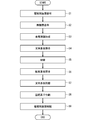
- FIG. It is a flowchart which shows the manufacturing method of the semiconductor element of Embodiment 1. It is sectional drawing which shows the manufacturing method of the semiconductor element of Embodiment 1. It is sectional drawing which shows the manufacturing method of the semiconductor element of Embodiment 1. It is sectional drawing which shows the manufacturing method of the semiconductor element of Embodiment 1. It is sectional drawing which shows the manufacturing method of the semiconductor element of Embodiment 1. It is sectional drawing which shows the manufacturing method of the semiconductor element of Embodiment 1. It is sectional drawing which shows the manufacturing method of the semiconductor element of Embodiment 1. It is sectional drawing which shows the manufacturing method of the semiconductor element of Embodiment 1. It is sectional drawing which shows the manufacturing method of the semiconductor element of Embodiment 1. It is sectional drawing which shows the manufacturing method of the semiconductor element of Embodiment 1.
- FIG. 1 is a cross-sectional view showing the configuration of the semiconductor element 101 of the first embodiment.
- the semiconductor element 101 includes a circuit element 2 and a transfer substrate 10.
- the transfer board 10 is joined to the lower surface of the circuit element 2.
- the circuit element 2 is a HEMT (high electron mobility transistor) having gallium nitride (GaN) as a semiconductor layer, but is a MOSFET (metal-oxide-semiconductor field-effect transistor) or an IGBT (insulated gate bipolar transistor). ) And other circuit elements may be used.
- the thickness of the circuit element 2 is, for example, 10 ⁇ m.
- the transfer substrate 10 is a substrate having high thermal conductivity, for example, a diamond substrate.
- FIG. 2 is a flowchart showing a manufacturing method of the semiconductor element 101. Hereinafter, a method of manufacturing the semiconductor element 101 will be described according to the flow of FIG.
- the circuit element substrate 7 includes a semiconductor substrate 1 and a circuit element 2 formed on the semiconductor substrate 1.
- the semiconductor substrate 1 is, for example, a Si wafer, a SiC (silicon carbide) wafer, or the like.
- the circuit element 2 includes a hollow bridge electrode connecting the electrodes, and although not shown in FIG. 3, there is a step due to the electrodes on the upper surface of the circuit element 2. It is necessary to form a protective layer on the circuit element 2 in order to prevent damage to the electrodes in the subsequent polishing step. Therefore, as shown in FIG. 4, the electrode protection layer 3 is coated and formed on the circuit element 2 (step S1). The electrode protection layer 3 not only protects the electrodes of the circuit element 2 in the subsequent polishing step, but also has the effect of increasing the bonding strength with the support substrate by flattening the irregularities of the electrodes.
- an adhesive composed of an organic solvent and a thermosetting resin or a photocurable resin, or a photoresist material, which can be removed by chemical treatment or oxygen ashing in the final step is selected.
- an acrylic resin, an olefin resin, a phenol resin, a polypropylene resin, a polyethylene resin, a polyethylene resin or the like is used for the electrode protective layer 3.
- a material having a high substrate strength in which the circuit element substrate 7 and the support substrate are integrated and which does not cause peeling or cracking in the polishing process is effective. From that viewpoint, an acrylic resin is effective.
- a material having high film strength such as epoxy resin is preferable.
- the electrode protective layer 3 For coating the electrode protection layer 3, for example, a spin coating method is used in which an adhesive is dropped on the main surface of the circuit element substrate 7 on which the circuit element 2 is formed, and the circuit element substrate 7 is rotated at high speed. However, other coating methods such as printing or spraying may be used.
- the electrode protective layer 3 has a thickness of 5 ⁇ m or more and 8 ⁇ m or less, and is formed so as to cover the circuit element 2. After applying the electrode protective layer 3 on the circuit element 2, the electrode protective layer 3 is cured.
- a thermosetting resin is used as the material of the electrode protective layer 3
- the solvent component evaporates and cures when the electrode protective layer 3 is heated to 90 ° C. or higher and 120 ° C. or lower by a hot plate or the like.
- a photocurable resin is used as the material of the electrode protective layer 3, the electrode protective layer 3 is cured by irradiating the circuit element substrate 7 with light.
- a release layer 5 is formed on the adhesive surface of the transparent substrate 4 to prepare the support substrate 8 (step S2). That is, the support substrate 8 includes a transparent substrate 4 and a release layer 5 formed on the transparent substrate 4.
- the transparent substrate 4 has light transmittance and is made of non-alkali glass, sapphire glass, or the like.
- the release layer 5 made of a photodegradable material that decomposes when it absorbs light such as laser or infrared rays is formed on the transparent substrate 4.
- a peeling layer 5 is formed by applying a paste composed of a resin containing a carbon material that absorbs light, generates heat, and thermally decomposes to a transparent substrate 4 by a spin coating method, and heat-drying the paste. ..
- a carbon film having a thickness of 1 ⁇ m or more and 2 ⁇ m or less may be formed as the release layer 5 on the transparent substrate 4 by a CVD sputtering device. When the carbon film is used for the release layer 5, the support substrate 8 can be firmly adhered to the circuit element substrate 7.
- the surface of the release layer 5 is mirror-finished by lapping polishing.
- the arithmetic mean roughness of the surface of the release layer 5 is preferably less than 0.5 nm, more preferably less than 0.2 nm. If the arithmetic mean roughness of the surface of the peeling layer 5 is less than 0.5 nm, it is possible to reduce the portion that is not adhered to the circuit element substrate 7 in the subsequent process, and the adhesive strength to the circuit element substrate 7 is increased.
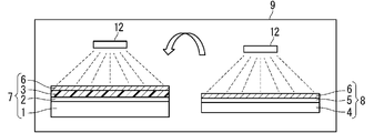
- the circuit element substrate 7 and the support substrate 8 are set in the vacuum chamber 9 and exhausted to an ultra-high vacuum of 10-6 Pa.
- a metal thin film 6 is formed on the electrode protection layer 3 of the circuit element substrate 7 and the release layer 5 of the support substrate 8 by a sputtering method or a vapor deposition method to a thickness of several nm or more and several tens of nm or less.
- FIG. 6 shows how sputter atoms are emitted from the sputtering target 12 onto the electrode protection layer 3.
- the material of the metal thin film 6 aluminum, copper, silicon, titanium, gold, silver, iron, chromium and the like are used.
- step S4 the metal thin films 6 are bonded to each other in the vacuum chamber 9 to join the circuit element substrate 7 and the support substrate 8 (step S4).
- step S3 The formation of the metal thin film 6 (step S3) and the joining of the circuit element substrate 7 and the support substrate 8 (step S4) are continuously performed in the same vacuum chamber 9. If the circuit element substrate 7 and the support substrate 8 are taken out into the atmosphere after the metal thin film 6 is formed, moisture, a natural oxide film or an organic substance adheres to the surface, and the metal thin films 6 do not bond to each other. Therefore, in order to bond the circuit element substrate 7 and the support substrate 8, it is necessary to irradiate the circuit element substrate 7 and the support substrate 8 with an ion beam or a neutral atom beam again in a vacuum to clean the circuit element substrate 7.
- step S3 and step S4 since the atomic diffusion bonding method is used in which the metal thin films 6 are formed on the circuit element substrate 7 and the support substrate 8 in a vacuum and then the metal thin films 6 are bonded to each other in the same vacuum, an atomic beam or the like is used. No need for surface activation by. Therefore, there is no loss in the process, and the process time of the joining step (step S3 and step S4) can be shortened from 10 minutes to 15 minutes. Therefore, if a cassette that can set several wafers at a time is used and a load lock chamber, which is a preliminary exhaust chamber, is provided in the vacuum chamber 9, it is compared with the process of attaching a substrate using a general adhesive. The processing time can be shortened.
- the thickness of the resin film is as thick as several hundred ⁇ m or more and several mm, and the elastic modulus of the resin film is small. .. Therefore, the substrate strength after bonding is low, and when the circuit element substrate 7 is polished to be thinned, cracks occur in the peripheral portion of the circuit element substrate 7 or the circuit element substrate 7 is peeled off from the support substrate 8. Problems occur.
- the thickness of the adhesive layer can be made very thin, from about 0.2 nm to 20 nm for one atom.
- the adhesive force is strong and the mechanical strength of the bonded substrate is high. Therefore, defects such as cracks, peeling or breakage during polishing or dicing are reduced.
- the substrate is not thermally expanded and distorted by heating. Therefore, the material of the substrate to be joined is not selected.
- the surface of the bonding substrate composed of the circuit element substrate 7 and the support substrate 8 on the circuit element substrate 7 side is polished to remove the semiconductor substrate 1 (step S5).
- the reason for removing the semiconductor substrate 1 is to improve the heat dissipation efficiency of the circuit element 2 and to obtain low power consumption and high output.
- the semiconductor substrate 1 having a thickness of 500 ⁇ m is polished to a thickness of 20 ⁇ m.
- the polishing method mechanical polishing, chemical polishing, chemical mechanical polishing, or the like is used.
- the remaining semiconductor substrate 1 having a thickness of 20 ⁇ m is removed by dry etching such as reactive ion etching (RIE).
- RIE reactive ion etching
- the semiconductor substrate 1 is completely removed, and the lower surface of the circuit element 2 is exposed. Then, chemical mechanical polishing is performed to obtain the flatness of the lower surface of the circuit element 2. It is desirable that the arithmetic average roughness Ra of the lower surface of the circuit element 2 is 0.5 nm or less in consideration of the bonding with the transfer substrate 10 to be performed later.
- the strength of the circuit element substrate 7 including the circuit element 2 decreases. Therefore, the circuit element 2 is deformed due to the influence of the stress of the residual film, and cracks or peeling occur in the peripheral portion of the circuit element 2 due to uneven polishing.
- the semiconductor substrate 1 is polished in a state where the circuit element substrate 7 is firmly adhered to the support substrate 8, the strength of the circuit element substrate 7 is maintained even if the semiconductor substrate 1 is removed. Therefore, defects such as deformation, cracking, and peeling of the circuit element 2 are suppressed.
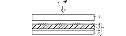
- the lower surface of the circuit element 2 is joined to the transfer substrate 10 (step S6).
- the transfer substrate 10 for example, a diamond substrate having excellent thermal conductivity is used.
- the transfer substrate 10 has a thickness of 100 ⁇ m, and the arithmetic average roughness of the joint surface is 0.5 nm or less by precision polishing.
- the same atomic diffusion bonding method as the bonding of the support substrate 8 described above is used.
- the coefficient of thermal expansion of diamond constituting the transfer substrate 10 is 2.3 ⁇ 10 -6 / K, which is significantly different from the coefficient of thermal expansion of gallium nitride constituting the circuit element 2 of 5.5 ⁇ 10 -6 / K. ..
- the circuit element 2 and the transfer substrate 10 may be bonded by irradiating the bonding surface with a neutral atom beam to remove the natural oxide film or the organic substance, and then using a surface activation method of bonding.
- the arithmetic average roughness of the joint surface between the circuit element 2 and the transfer substrate 10 is set to 0.5 nm or less by surface polishing.
- the support substrate 8 is peeled off from the circuit element substrate 7 (step S7). Specifically, the support substrate 8 is peeled off by irradiating a laser from the upper surface of the transparent substrate 4 to heat and decompose the peeling layer 5.
- the number of steps is small, the processing time is short, and the transparent substrate 4 can be reused, so that the productivity is improved and the productivity is improved. Production cost can be reduced.
- step S8 dicing is performed as shown in FIGS. 10 and 11, and the bonding substrate including the transfer substrate 10 and the circuit element substrate 7 is divided into a plurality of chips (step S8).
- FIG. 11 shows one chip after division. Many elements are formed in the circuit element 2, and each element is divided in this step.
- the dicing method laser dicing, plasma dicing or the like can be used. Conventionally, cracks, peeling, or chipping have occurred in the circuit element substrate 7 in the dicing process due to the decrease in strength due to the thinning.
- the circuit element substrate 7 is directly bonded to the support substrate 8 to increase the strength, the above-mentioned problems are suppressed.
- step S9 the metal thin film 6 and the electrode protective layer 3 are peeled off from the individualized chip.
- the circuit element substrate 7 is immersed in an alkaline or acidic stripping solution, an organic solvent, or the like, and the metal thin film 6 and the electrode protective layer 3 are dissolved and removed. Then, the residual organic matter is washed and the circuit element substrate 7 is dried.
- the metal thin film 6 may be removed with an acidic stripping solution, and the electrode protective layer 3 may be removed with oxygen ashing. In this way, the semiconductor element 101 shown in FIG. 1 is completed.
- a circuit element substrate 7 including the semiconductor substrate 1 and the circuit element 2 on the semiconductor substrate 1 is prepared, and an electrode is provided on the circuit element 2.
- a protective layer 3 is formed, a support substrate 8 is prepared, a metal thin film 6 is formed on the electrode protective layer 3 and the support substrate 8 of the circuit element substrate 7 in vacuum, and the circuit element substrate 7 and the support substrate 8 are formed.
- the substrates 10 are joined, and after the transfer substrate 10 is joined, the support substrate 8 is peeled off from the circuit element 2. Since the metal thin films 6 of the circuit element substrate 7 and the support substrate 8 are firmly bonded to each other by the atomic diffusion bonding method, the mechanical strength of the bonded substrate to which the circuit element substrate 7 and the support substrate 8 are bonded is increased. Therefore, even if the semiconductor substrate 1 is polished to make the semiconductor element thinner, defects such as cracks, peeling, or breakage are less likely to occur in the circuit element 2, and the defect rate can be lowered.
- FIG. 12 is a cross-sectional view of the semiconductor element 102 of the second embodiment.
- the semiconductor element 102 includes a circuit element 2, an inorganic insulating film 11 formed on the upper surface of the circuit element 2, and a transfer substrate 10 formed on the lower surface of the circuit element 2.
- the circuit element 2 and the transfer substrate 10 are as described in the first embodiment.
- the inorganic insulating film 11 is an electrode protective layer.
- the resin was used for the electrode protective layer 3 of the first embodiment, the inorganic insulating film having high thermal conductivity is used as the electrode protective layer in the second embodiment, so that this is referred to as the inorganic insulating film 11. Refer to.
- the strength of the bonding substrate between the circuit element substrate 7 and the support substrate 8 is improved as compared with the case where a resin is used, and cracks or peeling of the semiconductor substrate 1 after polishing are suppressed. be able to.
- the inorganic insulating film 11 is not removed and is used as a heat radiating material on the upper surface side of the circuit element 2, thereby improving the heat radiating performance of the semiconductor element 102 and omitting the step of removing the inorganic insulating film 11.
- the inorganic insulating film 11 is an inorganic insulating film having high thermal conductivity.
- FIG. 13 shows a semiconductor substrate 1 and a circuit element substrate 7 including a circuit element 2 on the semiconductor substrate 1. Since the circuit element 2 has a hollow bridge electrode connecting the electrodes, a step is formed on the upper surface of the circuit element 2 as shown in FIG. The height of this step is about several ⁇ m.
- the circuit element substrate 7 is put into a film forming apparatus such as a CVD plasma apparatus, and as shown in FIG. 14, an inorganic insulating film 11 having high thermal conductivity is formed on the circuit element 2 to be equal to or higher than the height of the electrode in the circuit element 2. It is formed with the thickness of.
- a film forming apparatus such as a CVD plasma apparatus
- an inorganic insulating film 11 having high thermal conductivity is formed on the circuit element 2 to be equal to or higher than the height of the electrode in the circuit element 2. It is formed with the thickness of.
- the material of the inorganic insulating film 11 diamond, aluminum nitride, silicon nitride, beryllium oxide or the like can be used.
- the electrode protective layer can be used as a heat sink on the upper surface side of the circuit element 2, so that the step of removing the electrode protective layer becomes unnecessary. Therefore, it is possible to shorten the process time and improve the device performance.
- the electrode protective layer 3 of the first embodiment is a resin
- the resin flows by using the spin coating method, and the upper surface of the electrode protective layer 3 is formed flat.
- the inorganic insulating film 11 is formed by a CVD method or the like, a step is formed on the upper surface of the inorganic insulating film 11 as shown in FIG.
- the high portion of the inorganic insulating film 11 is flattened to the same height as the electrodes of the circuit element 2 by a polishing method.
- the arithmetic mean roughness of the upper surface of the inorganic insulating film 11 at this time is 1.0 nm or less.
- Step S3 After cleaning the upper surface of the inorganic insulating film 11 to remove polishing residues, the formation of the metal thin film 6 (step S3), the circuit element substrate 7 (step S4), and the support substrate 8 are performed in the same manner as in the first embodiment.
- Step S5 polishing the semiconductor substrate 1 (step S6), joining the transfer substrate 10 (step S7), peeling the support substrate 8 (step S8), and dividing the circuit element 2 (step S9).
- the metal thin film 6 is removed from the upper surface of the inorganic insulating film 11, and the semiconductor element 102 shown in FIG. 12 is completed.
- the inorganic insulating film 11 remains on the upper surface of the circuit element 2 and functions as a heat sink.
- the electrode protective layer formed on the upper surface of the circuit element 2 is an inorganic insulating film 11 made of an inorganic insulating material. Therefore, as compared with the case where resin is used for the electrode protection layer, the strength of the bonding substrate between the circuit element substrate 7 and the support substrate 8 is improved, and cracks or peeling of the semiconductor substrate 1 after polishing can be suppressed.
- the inorganic insulating film 11 is an inorganic insulating film having high thermal conductivity, the inorganic insulating film 11 can be used not only as an electrode protective layer but also as a heat radiating material on the upper surface side of the circuit element 2. Therefore, the heat dissipation of the semiconductor element 102 can be improved, and the step of removing the electrode protective layer can be omitted.
Abstract
Description
<A-1.構成>
図1は、実施の形態1の半導体素子101の構成を示す断面図である。半導体素子101は回路素子2と転写基板10とを備える。転写基板10は回路素子2の下面に接合されている。以下の説明では、回路素子2を、窒化ガリウム(GaN)を半導体層として有するHEMT(high electron mobility transistor)とするが、MOSFET(metal-oxide-semiconductor field-effect transistor)またはIGBT(insulated gate bipolar transistor)など他の回路素子であっても良い。回路素子2の厚さは例えば10μmである。転写基板10は熱伝導率が高い基板であり、例えばダイヤモンド基板である。 <A.
<A-1. Configuration>
FIG. 1 is a cross-sectional view showing the configuration of the
図2は、半導体素子101の製造方法を示すフローチャートである。以下、図2のフローに沿って半導体素子101の製造方法を説明する。 <A-2. Manufacturing process>
FIG. 2 is a flowchart showing a manufacturing method of the
以上に説明したように、実施の形態1の半導体素子の製造方法によれば、半導体基板1と半導体基板1上の回路素子2とを備える回路素子基板7を用意し、回路素子2上に電極保護層3を形成し、支持基板8を用意し、真空中で回路素子基板7の電極保護層3上と支持基板8上とに金属薄膜6を形成し、回路素子基板7および支持基板8の金属薄膜6同士を原子拡散接合法により貼り合わせることにより、回路素子基板7および支持基板8を接合し、半導体基板1を研磨除去して回路素子2を露出し、回路素子2の露出面に転写基板10を接合し、転写基板10の接合後に支持基板8を回路素子2から剥離する。回路素子基板7と支持基板8の金属薄膜6同士が原子拡散接合法により強固に接着されるため、回路素子基板7と支持基板8を接合した接合基板の機械的強度が高くなる。従って、半導体基板1を研磨して半導体素子を薄くしても、回路素子2にクラック、剥離または破損などの不具合が生じにくく、不良率を低くすることができる。 <A-3. Effect>
As described above, according to the method for manufacturing a semiconductor element of the first embodiment, a
<B-1.構成>
図12は、実施の形態2の半導体素子102の断面図である。半導体素子102は、回路素子2と、回路素子2の上面に形成された無機絶縁膜11と、回路素子2の下面に形成された転写基板10とを備えている。回路素子2と転写基板10は実施の形態1で説明した通りである。無機絶縁膜11は電極保護層である。但し、実施の形態1の電極保護層3に樹脂が用いられたのに対して、実施の形態2では熱伝導性が高い無機絶縁膜を電極保護層として用いるため、これを無機絶縁膜11と称する。 <
<B-1. Configuration>
FIG. 12 is a cross-sectional view of the
図13から図15は、回路素子基板7の回路素子2上に電極保護層としての無機絶縁膜11を形成する様子を示した断面図である。図13は、半導体基板1と、半導体基板1上の回路素子2を含む回路素子基板7を示している。回路素子2には、電極と電極を接続する中空のブリッジ電極があるため、図13に示すように回路素子2の上面には段差が形成されている。この段差の高さは数μm程度である。 <B-2. Manufacturing process>
13 to 15 are cross-sectional views showing how an inorganic insulating
実施の形態2の半導体素子の製造方法において、回路素子2の上面に形成される電極保護層は無機絶縁材料からなる無機絶縁膜11である。従って、電極保護層に樹脂を用いる場合に比べて、回路素子基板7と支持基板8との接合基板の強度が向上し、半導体基板1の研磨後のクラックまたは剥離を抑制することができる。また、無機絶縁膜11が熱伝導率の高い無機絶縁膜である場合には、無機絶縁膜11を電極保護層としてだけでなく、回路素子2の上面側の放熱材として用いることができる。従って、半導体素子102の放熱性を高めると共に、電極保護層の除去工程を省略することができる。 <B-3. Effect>
In the method for manufacturing a semiconductor element according to the second embodiment, the electrode protective layer formed on the upper surface of the
Claims (8)
- 半導体基板と前記半導体基板上の回路素子とを備える回路素子基板を用意し、
前記回路素子上に電極保護層を形成し、
支持基板を用意し、
真空中で前記回路素子基板の前記電極保護層上と支持基板上とに金属薄膜を形成し、
前記回路素子基板および前記支持基板の前記金属薄膜同士を原子拡散接合法により貼り合わせることにより、前記回路素子基板および前記支持基板を接合し、
前記半導体基板を研磨除去して前記回路素子を露出し、
前記回路素子の露出面に転写基板を接合し、
前記転写基板の接合後に前記支持基板を前記回路素子から剥離する、
半導体素子の製造方法。 A circuit element substrate including the semiconductor substrate and the circuit element on the semiconductor substrate is prepared.
An electrode protective layer is formed on the circuit element,
Prepare a support board and
A metal thin film is formed on the electrode protective layer and the support substrate of the circuit element substrate in a vacuum.
The circuit element substrate and the support substrate are bonded by bonding the metal thin films of the circuit element substrate and the support substrate to each other by an atomic diffusion bonding method.
The semiconductor substrate is polished and removed to expose the circuit element.
A transfer substrate is bonded to the exposed surface of the circuit element, and the transfer substrate is bonded to the exposed surface of the circuit element.
After joining the transfer substrate, the support substrate is peeled off from the circuit element.
Manufacturing method of semiconductor elements. - 前記金属薄膜の形成と、前記回路素子基板および前記支持基板の接合とは、同じ真空チャンバー内で連続して行われる、
請求項1に記載の半導体素子の製造方法。 The formation of the metal thin film and the joining of the circuit element substrate and the support substrate are continuously performed in the same vacuum chamber.
The method for manufacturing a semiconductor device according to claim 1. - 前記支持基板は、透明基板と、前記透明基板上に形成された光分解性材料からなる剥離層とを備え、
前記金属薄膜は前記支持基板の前記剥離層上に形成され、
前記支持基板の剥離は、前記剥離層を光分解することにより行われる、
請求項1または請求項2に記載の半導体素子の製造方法。 The support substrate includes a transparent substrate and a release layer made of a photodegradable material formed on the transparent substrate.
The metal thin film is formed on the release layer of the support substrate, and is formed on the release layer.
The peeling of the support substrate is performed by photodecomposing the peeling layer.
The method for manufacturing a semiconductor device according to claim 1 or 2. - 前記剥離層はカーボン膜からなり、
前記支持基板の剥離は、前記透明基板の下面からレーザーを照射することにより前記剥離層を加熱分解することにより行われる、
請求項3に記載の半導体素子の製造方法。 The release layer is made of a carbon film and is made of a carbon film.
The peeling of the support substrate is performed by heat-decomposing the peeling layer by irradiating a laser from the lower surface of the transparent substrate.
The method for manufacturing a semiconductor device according to claim 3. - 前記電極保護層は、アクリル樹脂またはエポキシ樹脂からなる、
請求項1から請求項4のいずれか1項に記載の半導体素子の製造方法。 The electrode protective layer is made of an acrylic resin or an epoxy resin.
The method for manufacturing a semiconductor device according to any one of claims 1 to 4. - 前記電極保護層は無機絶縁材料からなる、
請求項1から請求項4のいずれか1項に記載の半導体素子の製造方法。 The electrode protective layer is made of an inorganic insulating material.
The method for manufacturing a semiconductor device according to any one of claims 1 to 4. - 前記無機絶縁材料は、ダイヤモンド、窒化アルミニウム、窒化ケイ素、および酸化ベリリウムのいずれかである、
請求項6に記載の半導体素子の製造方法。 The inorganic insulating material is either diamond, aluminum nitride, silicon nitride, and beryllium oxide.
The method for manufacturing a semiconductor device according to claim 6. - 前記回路素子は窒化ガリウムを半導体層として含み、
前記転写基板はダイヤモンドからなる、
請求項1から請求項7のいずれか1項に記載の半導体素子の製造方法。 The circuit element contains gallium nitride as a semiconductor layer.
The transfer substrate is made of diamond.
The method for manufacturing a semiconductor device according to any one of claims 1 to 7.
Priority Applications (6)
| Application Number | Priority Date | Filing Date | Title |
|---|---|---|---|
| PCT/JP2020/016312 WO2021210047A1 (en) | 2020-04-13 | 2020-04-13 | Method for manufacturing semiconductor element |
| US17/912,053 US20230134255A1 (en) | 2020-04-13 | 2020-04-13 | Method of manufacturing semiconductor element |
| JP2022514883A JP7186921B2 (en) | 2020-04-13 | 2020-04-13 | Semiconductor device manufacturing method |
| CN202080099340.8A CN115428127A (en) | 2020-04-13 | 2020-04-13 | Method for manufacturing semiconductor element |
| EP20931548.0A EP4138116B1 (en) | 2020-04-13 | 2020-04-13 | Method for manufacturing semiconductor element |
| KR1020227032511A KR20220143741A (en) | 2020-04-13 | 2020-04-13 | Method of manufacturing semiconductor device |
Applications Claiming Priority (1)
| Application Number | Priority Date | Filing Date | Title |
|---|---|---|---|
| PCT/JP2020/016312 WO2021210047A1 (en) | 2020-04-13 | 2020-04-13 | Method for manufacturing semiconductor element |
Publications (1)
| Publication Number | Publication Date |
|---|---|
| WO2021210047A1 true WO2021210047A1 (en) | 2021-10-21 |
Family
ID=78084736
Family Applications (1)
| Application Number | Title | Priority Date | Filing Date |
|---|---|---|---|
| PCT/JP2020/016312 WO2021210047A1 (en) | 2020-04-13 | 2020-04-13 | Method for manufacturing semiconductor element |
Country Status (6)
| Country | Link |
|---|---|
| US (1) | US20230134255A1 (en) |
| EP (1) | EP4138116B1 (en) |
| JP (1) | JP7186921B2 (en) |
| KR (1) | KR20220143741A (en) |
| CN (1) | CN115428127A (en) |
| WO (1) | WO2021210047A1 (en) |
Citations (5)
| Publication number | Priority date | Publication date | Assignee | Title |
|---|---|---|---|---|
| JPH1174230A (en) * | 1997-08-29 | 1999-03-16 | Nippon Telegr & Teleph Corp <Ntt> | Manufacture of thin-film semiconductor device |
| JP2005129825A (en) | 2003-10-27 | 2005-05-19 | Sumitomo Chemical Co Ltd | Manufacturing method of compound semiconductor substrate |
| JP2007188967A (en) * | 2006-01-11 | 2007-07-26 | Sony Corp | Substrate support, substrate treatment method, and method of manufacturing semiconductor device |
| JP2007324406A (en) | 2006-06-01 | 2007-12-13 | Sony Corp | Substrate treatment method and manufacturing method for semiconductor device |
| JP2012028477A (en) | 2010-07-22 | 2012-02-09 | Sumitomo Electric Ind Ltd | Method of manufacturing semiconductor device |
Family Cites Families (4)
| Publication number | Priority date | Publication date | Assignee | Title |
|---|---|---|---|---|
| US20140144593A1 (en) * | 2012-11-28 | 2014-05-29 | International Business Machiness Corporation | Wafer debonding using long-wavelength infrared radiation ablation |
| JP6299478B2 (en) * | 2013-06-26 | 2018-03-28 | 日亜化学工業株式会社 | Light emitting device and manufacturing method thereof |
| WO2015156381A1 (en) * | 2014-04-10 | 2015-10-15 | 富士電機株式会社 | Method for processing semiconductor substrate and method for manufacturing semiconductor device in which said processing method is used |
| JP7002398B2 (en) | 2018-04-13 | 2022-01-20 | 株式会社ディスコ | How to join optical components |
-
2020
- 2020-04-13 CN CN202080099340.8A patent/CN115428127A/en active Pending
- 2020-04-13 JP JP2022514883A patent/JP7186921B2/en active Active
- 2020-04-13 WO PCT/JP2020/016312 patent/WO2021210047A1/en unknown
- 2020-04-13 US US17/912,053 patent/US20230134255A1/en active Pending
- 2020-04-13 EP EP20931548.0A patent/EP4138116B1/en active Active
- 2020-04-13 KR KR1020227032511A patent/KR20220143741A/en not_active Application Discontinuation
Patent Citations (5)
| Publication number | Priority date | Publication date | Assignee | Title |
|---|---|---|---|---|
| JPH1174230A (en) * | 1997-08-29 | 1999-03-16 | Nippon Telegr & Teleph Corp <Ntt> | Manufacture of thin-film semiconductor device |
| JP2005129825A (en) | 2003-10-27 | 2005-05-19 | Sumitomo Chemical Co Ltd | Manufacturing method of compound semiconductor substrate |
| JP2007188967A (en) * | 2006-01-11 | 2007-07-26 | Sony Corp | Substrate support, substrate treatment method, and method of manufacturing semiconductor device |
| JP2007324406A (en) | 2006-06-01 | 2007-12-13 | Sony Corp | Substrate treatment method and manufacturing method for semiconductor device |
| JP2012028477A (en) | 2010-07-22 | 2012-02-09 | Sumitomo Electric Ind Ltd | Method of manufacturing semiconductor device |
Non-Patent Citations (1)
| Title |
|---|
| See also references of EP4138116A4 |
Also Published As
| Publication number | Publication date |
|---|---|
| JP7186921B2 (en) | 2022-12-09 |
| KR20220143741A (en) | 2022-10-25 |
| EP4138116A1 (en) | 2023-02-22 |
| EP4138116B1 (en) | 2024-03-13 |
| CN115428127A (en) | 2022-12-02 |
| JPWO2021210047A1 (en) | 2021-10-21 |
| EP4138116A4 (en) | 2023-07-19 |
| US20230134255A1 (en) | 2023-05-04 |
Similar Documents
| Publication | Publication Date | Title |
|---|---|---|
| JP6715345B2 (en) | Method of transferring device layer to transfer substrate | |
| TWI442485B (en) | Method for manufacturing semiconductor device | |
| TWI798236B (en) | Element substrate with high thermal conductivity and manufacturing method thereof | |
| JP3502036B2 (en) | Semiconductor device manufacturing method and semiconductor device | |
| JP7016445B2 (en) | Manufacturing method of semiconductor device | |
| CN111900200A (en) | Diamond-based gallium nitride composite wafer and bonding preparation method thereof | |
| WO2021210047A1 (en) | Method for manufacturing semiconductor element | |
| JP2022086775A (en) | Heat conduction structure of lsi element, and manufacturing method for lsi element including the heat conduction structure | |
| JP6775722B1 (en) | Polishing method, semiconductor substrate manufacturing method | |
| JP2005129653A (en) | Method of manufacturing semiconductor device | |
| CN113454758B (en) | Method for manufacturing semiconductor element | |
| WO2022168217A1 (en) | Method for manufacturing semiconductor substrate and method for manufacturing semiconductor device | |
| JP2008130705A (en) | Method of manufacturing semiconductor device | |
| WO2020235074A1 (en) | Method for manufacturing semiconductor substrate and method for manufacturing semiconductor device | |
| WO2020008882A1 (en) | Device-layer-transferred substrate production method and device layer-transferred substrate | |
| CN116856051A (en) | Preparation method of diamond-based gallium nitride wafer for reducing breakage probability of epitaxial layer | |
| JP2021118208A (en) | Method for manufacturing semiconductor device | |
| JP2010147353A (en) | Method for manufacturing semiconductor device |
Legal Events
| Date | Code | Title | Description |
|---|---|---|---|
| 121 | Ep: the epo has been informed by wipo that ep was designated in this application |
Ref document number: 20931548 Country of ref document: EP Kind code of ref document: A1 |
|
| ENP | Entry into the national phase |
Ref document number: 2022514883 Country of ref document: JP Kind code of ref document: A |
|
| ENP | Entry into the national phase |
Ref document number: 20227032511 Country of ref document: KR Kind code of ref document: A |
|
| NENP | Non-entry into the national phase |
Ref country code: DE |
|
| ENP | Entry into the national phase |
Ref document number: 2020931548 Country of ref document: EP Effective date: 20221114 |