WO2021200265A1 - Module de conversion thermoélectrique - Google Patents
Module de conversion thermoélectrique Download PDFInfo
- Publication number
- WO2021200265A1 WO2021200265A1 PCT/JP2021/011334 JP2021011334W WO2021200265A1 WO 2021200265 A1 WO2021200265 A1 WO 2021200265A1 JP 2021011334 W JP2021011334 W JP 2021011334W WO 2021200265 A1 WO2021200265 A1 WO 2021200265A1
- Authority
- WO
- WIPO (PCT)
- Prior art keywords
- electrode
- conversion module
- substrate
- element layer
- thermoelectric conversion
- Prior art date
Links
Images


Classifications
-
- H—ELECTRICITY
- H10—SEMICONDUCTOR DEVICES; ELECTRIC SOLID-STATE DEVICES NOT OTHERWISE PROVIDED FOR
- H10N—ELECTRIC SOLID-STATE DEVICES NOT OTHERWISE PROVIDED FOR
- H10N10/00—Thermoelectric devices comprising a junction of dissimilar materials, i.e. devices exhibiting Seebeck or Peltier effects
- H10N10/10—Thermoelectric devices comprising a junction of dissimilar materials, i.e. devices exhibiting Seebeck or Peltier effects operating with only the Peltier or Seebeck effects
- H10N10/17—Thermoelectric devices comprising a junction of dissimilar materials, i.e. devices exhibiting Seebeck or Peltier effects operating with only the Peltier or Seebeck effects characterised by the structure or configuration of the cell or thermocouple forming the device
-
- H—ELECTRICITY
- H01—ELECTRIC ELEMENTS
- H01L—SEMICONDUCTOR DEVICES NOT COVERED BY CLASS H10
- H01L23/00—Details of semiconductor or other solid state devices
- H01L23/34—Arrangements for cooling, heating, ventilating or temperature compensation ; Temperature sensing arrangements
- H01L23/38—Cooling arrangements using the Peltier effect
-
- H—ELECTRICITY
- H10—SEMICONDUCTOR DEVICES; ELECTRIC SOLID-STATE DEVICES NOT OTHERWISE PROVIDED FOR
- H10N—ELECTRIC SOLID-STATE DEVICES NOT OTHERWISE PROVIDED FOR
- H10N10/00—Thermoelectric devices comprising a junction of dissimilar materials, i.e. devices exhibiting Seebeck or Peltier effects
- H10N10/80—Constructional details
- H10N10/81—Structural details of the junction
- H10N10/817—Structural details of the junction the junction being non-separable, e.g. being cemented, sintered or soldered
-
- H—ELECTRICITY
- H10—SEMICONDUCTOR DEVICES; ELECTRIC SOLID-STATE DEVICES NOT OTHERWISE PROVIDED FOR
- H10N—ELECTRIC SOLID-STATE DEVICES NOT OTHERWISE PROVIDED FOR
- H10N10/00—Thermoelectric devices comprising a junction of dissimilar materials, i.e. devices exhibiting Seebeck or Peltier effects
- H10N10/80—Constructional details
- H10N10/85—Thermoelectric active materials
- H10N10/851—Thermoelectric active materials comprising inorganic compositions
- H10N10/852—Thermoelectric active materials comprising inorganic compositions comprising tellurium, selenium or sulfur
-
- H—ELECTRICITY
- H10—SEMICONDUCTOR DEVICES; ELECTRIC SOLID-STATE DEVICES NOT OTHERWISE PROVIDED FOR
- H10N—ELECTRIC SOLID-STATE DEVICES NOT OTHERWISE PROVIDED FOR
- H10N10/00—Thermoelectric devices comprising a junction of dissimilar materials, i.e. devices exhibiting Seebeck or Peltier effects
- H10N10/10—Thermoelectric devices comprising a junction of dissimilar materials, i.e. devices exhibiting Seebeck or Peltier effects operating with only the Peltier or Seebeck effects
- H10N10/13—Thermoelectric devices comprising a junction of dissimilar materials, i.e. devices exhibiting Seebeck or Peltier effects operating with only the Peltier or Seebeck effects characterised by the heat-exchanging means at the junction
Definitions
- the present invention relates to a thermoelectric conversion module.
- thermoelectric conversion module that uses a thermoelectric conversion material having a thermoelectric effect such as the Seebeck effect and the Perche effect to convert between thermal energy and electrical energy.
- thermoelectric conversion module a configuration of a so-called ⁇ -type thermoelectric conversion element is known.
- ⁇ -type for example, a pair of electrodes that are separated from each other are provided on the substrate, and the lower surface of the P-type thermoelectric element is provided on the one electrode and the lower surface of the N-type thermoelectric element is provided on the other electrode.
- the P-type thermoelectric element and the N-type thermoelectric element are provided apart from each other, and the upper surfaces of the P-type thermoelectric elements and the N-type thermoelectric elements are bonded to the electrodes of the opposing substrates (hereinafter, may be referred to as “PN junction”).
- PN junction the electrodes of the opposing substrates
- a plurality of pairs of PN-junctioned P-type thermoelectric elements and N-type thermoelectric elements are used, and are configured to be electrically connected in series and thermally connected in parallel.
- thermoelectric conversion module In recent years, electronic devices such as computers, mirrorless cameras, and mobile terminals such as smartphones have semiconductor elements such as CPUs (Central Processing Units), CMOSs (Complementary Metal Oxide Semiconductors), and light emitting diodes that operate and control them. It has become commonplace for electronic devices represented by Moreover, it has become a heating element that releases a large amount of heat. Under such circumstances, there is a demand for a cooling device that more efficiently absorbs and dissipates heat generated by the semiconductor element or the like. As one of the corresponding methods, electronic cooling or the like using the thermoelectric conversion module is used.
- a Pelche element is used as a cooling element in which a heat absorbing surface is bonded to the surface of the electronic element on the substrate, and further connected to the heat radiating surface side of the cooling element to dissipate heat from the electronic element.
- a metal plate having a surface area larger than the surface area of the cooling element and less than the surface area of the substrate, and a heat conductive sheet having a surface area larger than the surface area of the heat radiating surface of the cooling element and less than the surface area of the substrate.
- a heat dissipation structure with a pedestal including a heat conductive sheet in which one side is joined to the plate material and the other side is joined to the heat dissipation surface of the cooling element.
- the structure that dissipates heat from the electronic element on the substrate further heats the pedestal in which the metal plate material and the heat conductive sheet are joined to the heat radiating surface of the Pelche element used as the cooling element.
- the heat conductive sheet for example, a pair of heat conductive metal plates sandwiching a graphite sheet from both sides are used, which complicates the configuration, adds a manufacturing process, complicates mounting, and materials. It may be a problem from the viewpoint of cost increase.
- thermoelectric conversion module having a simple configuration and further improved heat dissipation.
- the present inventors have determined the area of the second electrode used for forming the PN junction pair of the P-type thermoelectric element and the N-type thermoelectric element constituting the thermoelectric conversion module.
- the present invention has been completed by finding that the heat dissipation from the surface of the second electrode is further improved by making the area larger than the area of the first electrode used for forming the opposing PN junction pair. That is, the present invention provides the following (1) to (6).
- the P-type thermoelectric element layer includes a first electrode, a P-type thermoelectric element layer, an N-type thermoelectric element layer, and a second electrode arranged so as to face the first electrode.
- thermoelectric conversion module connected in series to the above, wherein the area of the second electrode is larger than the area of the first electrode.
- the thermoelectric conversion module according to (1) above wherein the ratio R of the area of the second electrode to the area of the first electrode is 1.20 or more.
- the thermoelectric conversion module according to (1) or (2) above further including a first substrate and / or a second substrate.
- thermoelectric conversion module according to any one of (1) to (3) above, wherein the extending portion of the second electrode is thermally connected to a member made of a highly thermally conductive material.
- the second substrate has a through hole, and the second electrode is formed with the through hole interposed therebetween on both sides of the second substrate, and the P-type of the second electrode.
- the thermoelectric element layer and the other electrode surface side opposite to one electrode surface side on the N-type thermoelectric element layer side are the P-type thermoelectric element layer and the N-type thermoelectric element layer side of the second substrate.
- the thermoelectric conversion module according to any one of (1) to (4) above, which extends on a second substrate on the opposite side and is arranged as a continuous layer.
- thermoelectric conversion module is arranged inside the through hole of the second substrate, and the second electrode of the thermoelectric conversion module extends on the second substrate with the through hole interposed therebetween.
- the thermoelectric conversion module according to any one of (1) to (5) above, which is present and arranged as a continuous layer.
- thermoelectric conversion module having further improved heat dissipation with a simple configuration.
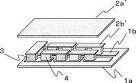
- thermoelectric conversion module which concerns on 1st Embodiment of this invention. It is a perspective view for demonstrating an example of the structure of the conventional thermoelectric conversion module. It is a transmission perspective view for demonstrating the structure of the thermoelectric conversion module which concerns on 2nd Embodiment of this invention. It is sectional drawing which shows the structure of the thermoelectric conversion module which concerns on 3rd Embodiment of this invention. It is sectional drawing which shows the structure of the thermoelectric conversion module which concerns on 4th Embodiment of this invention.
- thermoelectric conversion module includes a first electrode, a P-type thermoelectric element layer and an N-type thermoelectric element layer, and a second electrode arranged to face the first electrode, and the P A plurality of pairs of PN junctions in which the type thermoelectric element layer and the N-type thermoelectric element layer are PN-bonded with the first electrode or the second electrode interposed therebetween, the first electrode and the second electrode. It is a thermoelectric conversion module electrically connected in series alternately, wherein the area of the second electrode is larger than the area of the first electrode.
- thermoelectric conversion module of the present invention by making the area of the second electrode constituting the thermoelectric conversion module larger than the area of the first electrode, for example, the object to be cooled so that the first electrode side becomes an endothermic surface.
- the thermoelectric conversion module is energized after arranging the above, the heat generated from the object to be cooled can be efficiently dissipated from the second electrode.
- the positional relationship between the endothermic side and the heat radiating side is usually reversed depending on the direction of energization. Further, the polarity of the output is switched by switching the endothermic side and the heat radiating side. Therefore, the present invention is not limited as to which electrode is on the endothermic side or the heat radiating side.
- the second electrode side is described as the heat dissipation side
- the first electrode side is described as the endothermic side.
- thermoelectric conversion module of the present invention it is preferable to further include a first substrate and / or a second substrate.
- the heat dissipation distribution generated by the second electrode is made uniform, and the heat dissipation property is further improved.
- FIG. 1 is a transmission perspective view (visualizing a component portion) for explaining the configuration of the thermoelectric conversion module according to the first embodiment of the present invention
- FIG. 1A is a transmission perspective view showing an aspect of arrangement of a second electrode.
- (b) is a transmission perspective view which shows the whole structure of a thermoelectric conversion module.
- the thermoelectric conversion module according to the embodiment of the present invention is configured as a so-called ⁇ -type thermoelectric conversion element, for example, a first substrate 1a having a first electrode 1b, a P-type thermoelectric element layer 3 and an N-type thermoelectric element. It includes a layer 4 and a second electrode 2b arranged to face the first electrode 1b, and further includes a second substrate 2a on the second electrode 2b.
- the area of the second electrode 2b is larger than the area of the first electrode 1b.
- a plurality of PN junction pairs in which the P-type thermoelectric element layer 3 and the N-type thermoelectric element layer 4 are PN-junctioned with the first electrode 1b or the second electrode 2b interposed therebetween are the first pair.
- the electrode 1 and the second electrode are alternately electrically connected in series and thermally connected in parallel.
- the PN junction pair composed of the P-type thermoelectric element layer 3 and the N-type thermoelectric element layer 4 is not particularly limited, and is usually a plurality of pairs, and can be appropriately adjusted and used.
- FIG. 2 is a perspective view for explaining an example of the configuration of a conventional thermoelectric conversion module.
- the conventional thermoelectric conversion module is configured as a ⁇ -type thermoelectric conversion element.
- a first substrate 1a having a first electrode 1b, a P-type thermoelectric element layer 3 and an N-type thermoelectric element layer 4, and the above-mentioned first.
- It includes a second electrode 2b'arranged so as to face the electrode 1b of 1, and further includes a second substrate 2a'on the second electrode 2b'.
- electrodes having approximately the same area are usually used.
- the surface of the first substrate 1a opposite to the first electrode 1b side is an endothermic surface, and the other surface, the second electrode 2b or the second substrate 2a.
- the surface opposite to the second electrode 2b side of the above can be used as the heat radiating surface.
- the object to be cooled is arranged on the endothermic surface and joined.
- the object to be cooled is not particularly limited, and examples thereof include an electronic element and the like. Among these, it is preferable to cool the electronic element from the viewpoint of efficient cooling in a short time.
- Examples of the electronic element include heat-generating electronic components such as a CPU, CMOS, a light emitting diode, a semiconductor laser, and a capacitor, and usually include those arranged in a mounting portion of a circuit board.
- the number of objects to be cooled is not particularly limited and may be a plurality.
- Examples of the method of joining with the object to be cooled include known methods such as bonding with an adhesive and soldering.
- the ratio R of the area of the second electrode to the area of the first electrode (hereinafter, the ratio R of the area of the second electrode to the area of the first electrode is referred to as "ratio R". )
- the ratio R depends on the electrode material used, but when the same electrode material is used, it is preferably 1.2 or more, and more preferably 1.5 ⁇ R ⁇ 100.0. It is more preferably 2.0 ⁇ R ⁇ 50.0, even more preferably 4.0 ⁇ R ⁇ 25.0, and particularly preferably 6.0 ⁇ R ⁇ 16.0.
- the ratio R is in this range, the heat dissipation property is improved, and the object to be cooled can reach and maintain a predetermined temperature in a shorter time.
- thermoelectric element layers such as the P-type thermoelectric element layer 3 and the N-type thermoelectric element layer 4 constituting the thermoelectric conversion module is not particularly limited, but from the viewpoint of increasing the area of the second electrode 2b, for example, As shown in FIG. 1, it is preferable to arrange them so as to have two rows and a plurality of columns. However, when the thermoelectric element layers are arranged in a plurality of rows and in a plurality of columns, the periphery of the plurality of thermoelectric element layers may be arranged so as to be surrounded by other adjacent thermoelectric element layers.
- thermoelectric element layer arranged in the second row in the center all the surroundings are surrounded by adjacent thermoelectric element layers, and the arrangement is physically close to each other. May become.
- the area of the second electrode 2b may be appropriately increased within a range in which the electrical connection and the thermal connection to the thermoelectric conversion module of the present invention are not impaired and the ratio R is satisfied. It is preferable to adjust it so that it becomes large.
- the total area of the joint surfaces of the P-type thermoelectric element layer 3 and the N-type thermoelectric element layer 4 with respect to the electrodes is not particularly limited, but is usually smaller than the area of the electrodes. Further, from the viewpoint of uniformity of performance balance and ease of manufacture of the PN junction pair, it is preferable to use the same size.
- the heat from the cooling object is the first.
- Heat is absorbed from the endothermic surface on the substrate 1a side, and heat is dissipated from the second substrate 2a side having the second electrode 2b. Since the area of the second electrode 2b is larger than the area of the first electrode 1b, heat is efficiently and sufficiently dissipated from the second substrate 2a.
- the thermoelectric conversion module having such a configuration can efficiently dissipate the heat generated by the object to be cooled.
- thermoelectric conversion module of the present invention it is preferable that the extending portion of the second electrode is thermally connected to a member made of a highly thermally conductive material.
- the extending portion means a region in which the second electrode extends in the horizontal direction.
- FIG. 3 is a transmission perspective view for explaining the configuration of the thermoelectric conversion module according to the second embodiment of the present invention (visualization of the component portion).
- the first substrate 1a having the first electrode 1b, the P-type thermoelectric element layer 3 and the N-type thermoelectric element layer 4 and a second electrode 2b arranged to face the first electrode 1b, and further include a second substrate 2a on the second electrode 2b.
- each electrode is further extended in the direction of a space portion not occupied by another thermoelectric element layer, and is thermally connected to a member 5 made of a highly thermally conductive material.
- the electrode 2b'' is arranged on the second substrate 2a using an electrode having the same specifications as the second electrode 2b from the viewpoint of heat dissipation.
- the highly thermally conductive material used for the member 5 examples include ceramic materials such as aluminum nitride, silicon nitride, and alumina having high insulating properties and thermal conductivity.
- the dimensions of the member 5 are not particularly limited as long as the heat dissipation can be maintained.
- the heat from the cooling object is the first.
- the heat is absorbed from the endothermic surface on the substrate 1a side, and is dissipated from the second substrate 2a side having the second electrode 2b and the electrode 2b ′′, and is stored in the member 5 and dissipated. Since the area of the second electrode 2b (including the electrode 2b'') is larger than the area of the first electrode 1b and further includes the member 5, heat is dissipated more efficiently, quickly and sufficiently than in the first embodiment. Will be done. With the thermoelectric conversion module having such a configuration, the heat generated by the object to be cooled can be dissipated more efficiently.
- the second substrate has through holes, and the second electrodes are formed on both sides of the second substrate with the through holes interposed therebetween, and are electrically and electrically. It is preferably thermally connected. Further, the P-type thermoelectric element layer and the other electrode surface side of the second electrode opposite to one electrode surface side of the P-type thermoelectric element layer and the N-type thermoelectric element layer side are the P-type of the second substrate. It is preferable that the thermoelectric element layer extends on the second substrate on the side opposite to the N-type thermoelectric element layer side and is arranged as a continuous layer. Further, one of the electrode surface sides of the second electrode, which is the P-type thermoelectric element layer and the N-type thermoelectric element layer side, extends on the second substrate through the opening end of the through hole. It may be arranged as a continuous layer.
- FIG. 4 is a cross-sectional view showing the configuration of the thermoelectric conversion module according to the third embodiment of the present invention.
- the thermoelectric conversion module according to the third embodiment of the present invention includes a first substrate 11a having a first electrode 11b, a P-type thermoelectric element layer 13 and an N-type thermoelectric element layer 14, and the first electrode 11b. It includes a second electrode 12b arranged so as to face each other and a second substrate 12a.
- the second electrode 12b is formed on both sides of the second substrate 12a with through holes 17 interposed therebetween and is electrically and thermally connected.
- the second electrode 12b on the P-type thermoelectric element layer 13 and N-type thermoelectric element layer 14 side and the other electrode surface side of the second electrode 12b on the opposite side are the first. It extends on the substrate 12a of No. 2 and is arranged as a continuous layer. The area of the second electrode 12b having a continuous layer provided on the second substrate 12a can be further expanded. It is preferable that the second electrode 12b is appropriately adjusted within a range in which the electrical connection and the thermal connection to the thermoelectric element layer are not impaired and the ratio R is satisfied (not shown).
- the cooling object 16 is thermally connected to, for example, the first substrate 11a side.
- the through holes 17 can be formed by a known method. For example, it can be formed by drilling or plating. The through hole 17 may be filled with a metal material or the like. The filling improves the heat exhaust efficiency.
- the heat from the electronic element is generated by the first substrate by arranging the electronic element as the cooling object 16 with the side of the first substrate 11a having the first electrode 11b as the endothermic surface. Heat is absorbed from the endothermic surface on the 11a side, and heat is dissipated from the second electrode 12b. Since the second electrode 12b extends through the through hole 17 of the second substrate 12a and the front surface is enlarged and arranged as a continuous layer on the back surface side, efficient heat dissipation is performed quickly and sufficiently. With the thermoelectric conversion module having such a configuration, the heat generated by the electronic element as the cooling object 16 can be dissipated more efficiently.
- thermoelectric conversion module In the configuration of the thermoelectric conversion module of the present invention, the thermoelectric conversion module is arranged inside the through hole of the second substrate, and the second electrode of the thermoelectric conversion module extends on the second substrate. It is preferable that the layers are arranged as a continuous layer.
- FIG. 5 is a cross-sectional view showing the configuration of the thermoelectric conversion module according to the fourth embodiment of the present invention.
- the first electrode 11b, the P-type thermoelectric element layer 13 and the N-type thermoelectric element layer 14, and the first electrode 11b are arranged to face each other. 2 electrodes 12b and 2 are included.
- the P-type thermoelectric element layer 13 and the N-type thermoelectric element layer 14 are arranged inside the second substrate 12a, and the second electrode 12b extends to the back surface side of the second substrate 12a and is continuous. Arranged as a layer.
- the second electrode 12b is appropriately adjusted within a range in which the electrical connection and the thermal connection to the thermoelectric element layer are not impaired and the ratio R is satisfied (not shown).
- the object to be cooled 16 is thermally connected to, for example, the first electrode 11b.
- the heat from the electronic element is flush with the second substrate 12a.
- Heat is absorbed from the endothermic surface on the side of the first electrode 11b, and heat is dissipated from the second electrode 12b.
- the second electrode 12b is expanded and arranged as a continuous layer on the back surface side of the second substrate 12a, heat dissipation is efficiently and sufficiently performed.
- the thermoelectric conversion module having such a configuration, the heat generated by the electronic element as the cooling object 16 can be dissipated more efficiently.
- the P-type thermoelectric element layer and the N-type thermoelectric element layer used in the present invention are not particularly limited, but consist of a thermoelectric semiconductor material, a heat-resistant resin, and a thermoelectric semiconductor composition containing an ionic liquid and / or an inorganic ionic compound. Is preferable.
- thermoelectric semiconductor material used for the thermoelectric element layer is preferably pulverized to a predetermined size by, for example, a fine pulverizer or the like and used as thermoelectric semiconductor particles (hereinafter, the thermoelectric semiconductor material may be referred to as "thermoelectric semiconductor particles"). .).
- the particle size of the thermoelectric semiconductor particles is preferably 10 nm to 100 ⁇ m, more preferably 20 nm to 50 ⁇ m, and even more preferably 30 nm to 30 ⁇ m.
- the average particle size of the thermoelectric semiconductor fine particles was obtained by measuring with a laser diffraction type particle size analyzer (Mastersizer 3000 manufactured by Malvern), and was used as the median value of the particle size distribution.
- thermoelectric semiconductor material constituting the P-type thermoelectric element layer and the N-type thermoelectric element layer is any material that can generate a thermoelectric force by imparting a temperature difference.
- the present invention is not particularly limited, and for example, a bismuth-tellu thermoelectric semiconductor material such as P-type bismasterlide and N-type bismasterlide; a telluride thermoelectric semiconductor material such as GeTe and PbTe; an antimony-tellu thermoelectric semiconductor material; ZnSb, Zn 3 Sb.
- Zinc-antimon thermoelectric semiconductor materials such as 2, Zn 4 Sb 3 ; silicon-germanium thermoelectric semiconductor materials such as SiGe; bismus selenide thermoelectric semiconductor materials such as Bi 2 Se 3 ; ⁇ -FeSi 2 , CrSi 2, MnSi VDD-based thermoelectric semiconductor materials such as 1.73 and Mg 2 Si; oxide-based thermoelectric semiconductor materials; Whistler materials such as FeVAL, FeVALSi, and FeVTiAl, and sulfide-based thermoelectric semiconductor materials such as TiS 2 are used.
- thermoelectric semiconductor material used in the present invention is preferably a bismuth-tellurium-based thermoelectric semiconductor material such as P-type bismuthellide or N-type bismuthellide.
- P-type bismuth telluride one having a hole as a carrier and a positive Seebeck coefficient, for example, represented by Bi X Te 3 Sb 2-X is preferably used.
- X is preferably 0 ⁇ X ⁇ 0.8, more preferably 0.4 ⁇ X ⁇ 0.6.
- X is larger than 0 and 0.8 or less, the Seebeck coefficient and the electric conductivity become large, and the characteristics as a P-type thermoelectric conversion material are maintained, which is preferable.
- N-type bismuth telluride one having an electron carrier and a negative Seebeck coefficient, for example, represented by Bi 2 Te 3-Y Se Y is preferably used.
- the Seebeck coefficient and the electric conductivity become large, and the characteristics as an N-type thermoelectric conversion material are maintained, which is preferable.
- the blending amount of the thermoelectric semiconductor particles in the thermoelectric semiconductor composition is preferably 30 to 99% by mass. It is more preferably 50 to 96% by mass, and even more preferably 70 to 95% by mass.
- the Seebeck coefficient absolute value of the Perche coefficient
- the decrease in the electric conductivity is suppressed, and only the thermal conductivity is decreased, so that high thermoelectric performance is exhibited.
- a film having sufficient film strength and flexibility can be obtained, which is preferable.
- thermoelectric semiconductor particles are annealed (hereinafter, may be referred to as "annealing treatment A").
- annealing treatment A By performing the annealing treatment A, the crystallinity of the thermoelectric semiconductor particles is improved, and the surface oxide film of the thermoelectric semiconductor particles is removed, so that the Seebeck coefficient (absolute value of the Perche coefficient) of the thermoelectric conversion material is increased. , The thermoelectric performance index can be further improved.
- the heat-resistant resin used in the present invention acts as a binder between thermoelectric semiconductor particles and enhances the flexibility of the thermoelectric element layer.
- the heat-resistant resin is not particularly limited, but when a thin film made of a thermoelectric semiconductor composition is subjected to crystal growth of thermoelectric semiconductor particles by annealing or the like, various factors such as mechanical strength and thermal conductivity as a resin are obtained. Use a heat-resistant resin that maintains its physical properties without being impaired.
- the heat-resistant resin include polyamide resins, polyamideimide resins, polyimide resins, polyetherimide resins, polybenzoxazole resins, polybenzoimidazole resins, epoxy resins, and copolymers having a chemical structure of these resins.
- the heat-resistant resin may be used alone or in combination of two or more.
- polyamide resins, polyamide-imide resins, polyimide resins, and epoxy resins are preferable and have excellent flexibility because they have higher heat resistance and do not adversely affect the crystal growth of thermoelectric semiconductor particles in the thin film. Therefore, polyamide resin, polyamide-imide resin, and polyimide resin are more preferable.
- the polyimide resin is more preferable as the heat-resistant resin from the viewpoint of adhesion to the polyimide film and the like.
- the polyimide resin is a general term for polyimide and its precursor.
- the heat-resistant resin preferably has a decomposition temperature of 300 ° C. or higher.
- the decomposition temperature is within the above range, the flexibility of the thermoelectric element layer can be maintained without losing the function as a binder even when the thin film made of the thermoelectric semiconductor composition is annealed, as will be described later.
- the blending amount of the heat-resistant resin in the thermoelectric semiconductor composition is preferably 0.1 to 40% by mass, more preferably 0.5 to 20% by mass, and further preferably 1 to 20% by mass.
- a film having both high thermoelectric performance and film strength can be obtained.
- the ionic liquid that can be contained in the thermoelectric semiconductor composition is a molten salt formed by combining a cation and an anion, and refers to a salt that can exist as a liquid in any temperature range of ⁇ 50 ° C. or higher and lower than 400 ° C.
- the ionic liquid is an ionic compound having a melting point in the range of ⁇ 50 ° C. or higher and lower than 400 ° C.
- the melting point of the ionic liquid is preferably ⁇ 25 ° C. or higher and 200 ° C. or lower, and more preferably 0 ° C. or higher and 150 ° C. or lower.
- Ionic liquids have features such as extremely low vapor pressure, non-volatility, excellent thermostability and electrochemical stability, low viscosity, and high ionic conductivity. Therefore, as a conductive auxiliary agent, it is possible to effectively suppress a decrease in electrical conductivity between thermoelectric semiconductor materials. Further, since the ionic liquid exhibits high polarity based on the aprotic ionic structure and has excellent compatibility with the heat-resistant resin, the electric conductivity of the thermoelectric conversion material can be made uniform.
- ionic liquid known or commercially available ones can be used.
- nitrogen-containing cyclic cation compounds such as pyridinium, pyrimidinium, pyrazolium, pyrrolidinium, piperidinium, imidazolium and their derivatives; tetraalkylammonium-based amine-based cations and their derivatives; phosphonium, trialkylsulfonium, tetraalkylphosphonium and the like.
- phosphine cations and derivatives thereof and a cationic component such as lithium cations and derivatives thereof, Cl -, Br -, I -, AlCl 4 -, Al 2 Cl 7 -, BF 4 -, PF 6 -, ClO 4 -, NO 3 -, CH 3 COO - , CF 3 COO -, CH 3 SO 3 -, CF 3 SO 3 -, (FSO 2) 2 N -, (CF 3 SO 2) 2 N -, (CF 3 SO 2) 3 C -, AsF 6 -, SbF 6 -, NbF 6 -, TaF 6 -, F (HF) n -, (CN) 2 n -, C 4 F 9 SO 3 -, (C 2 F 5 SO 2) Examples thereof include those composed of anionic components such as 2 N ⁇ , C 3 F 7 COO ⁇ , and (CF 3 SO 2 ) (CF 3 CO) N ⁇ .
- the cation component of the ionic liquid is a pyridinium cation and its derivatives from the viewpoints of high temperature stability, compatibility with thermoelectric semiconductor materials and resins, and suppression of decrease in electrical conductivity between thermoelectric semiconductor material gaps.
- 1-butyl-4-methylpyridinium bromide, 1-butylpyridinium bromide, and 1-butyl-4-methylpyridinium hexafluorophosphate are preferable.
- the cation component is [1-butyl-3- (2-hydroxyethyl) imidazolium bromide], [1-butyl-3- (2-hydroxyethyl) imidazole].
- Rium tetrafluoroborate] is preferable.
- the above-mentioned ionic liquid preferably has a decomposition temperature of 300 ° C. or higher. As long as the decomposition temperature is within the above range, the effect as a conductive auxiliary agent can be maintained even when the thin film made of the thermoelectric semiconductor composition is annealed, as will be described later.
- the blending amount of the ionic liquid in the thermoelectric semiconductor composition is preferably 0.01 to 50% by mass, more preferably 0.5 to 30% by mass, and further preferably 1.0 to 20% by mass.
- the blending amount of the ionic liquid is within the above range, the decrease in electrical conductivity is effectively suppressed, and a film having high thermoelectric performance can be obtained.
- the inorganic ionic compound that can be contained in the thermoelectric semiconductor composition is a compound composed of at least cations and anions. Since the inorganic ionic compound exists as a solid in a wide temperature range of 400 to 900 ° C. and has characteristics such as high ionic conductivity, it can be used as a conductivity auxiliary agent to reduce the electrical conductivity between thermoelectric semiconductor materials. Can be suppressed.
- the blending amount of the inorganic ionic compound in the thermoelectric semiconductor composition is preferably 0.01 to 50% by mass, more preferably 0.5 to 30% by mass, and further preferably 1.0 to 10% by mass.
- the blending amount of the inorganic ionic compound is within the above range, the decrease in electrical conductivity can be effectively suppressed, and as a result, a film having improved thermoelectric performance can be obtained.
- the total content of the inorganic ionic compound and the ionic liquid in the thermoelectric semiconductor composition is preferably 0.01 to 50% by mass, more preferably. Is 0.5 to 30% by mass, more preferably 1.0 to 10% by mass.
- thermoelectric element layer made of the thermoelectric semiconductor composition can be formed, for example, by applying the thermoelectric semiconductor composition on a substrate and drying it. By forming in this way, a large number of thermoelectric conversion element layers can be easily obtained at low cost.
- a method of applying a thermoelectric semiconductor composition to obtain a thermoelectric element layer a screen printing method, a flexographic printing method, a gravure printing method, a spin coating method, a dip coating method, a die coating method, a spray coating method, a bar coating method, and a doctor blade
- Known methods such as a method can be mentioned and are not particularly limited.
- thermoelectric element layer When the coating film is formed into a pattern, a screen printing method, a slot die coating method, or the like, which enables easy pattern formation using a screen plate having a desired pattern, is preferably used. Then, the obtained coating film is dried to form a thermoelectric element layer.
- the thickness of the thermoelectric element layer is not particularly limited, and is preferably 100 nm to 1000 ⁇ m, more preferably 300 nm to 600 ⁇ m, and further preferably 5 to 400 ⁇ m from the viewpoint of thermoelectric performance and film strength.
- the P-type thermoelectric element layer and the N-type thermoelectric element layer as a thin film made of the thermoelectric semiconductor composition are further subjected to an annealing treatment (hereinafter, may be referred to as "annealing treatment B").
- annealing treatment B By performing the annealing treatment B, the thermoelectric performance can be stabilized, and the thermoelectric semiconductor particles in the thin film can be crystal-grown, so that the thermoelectric performance can be further improved.
- the annealing treatment B is not particularly limited, but is usually carried out under an inert gas atmosphere such as nitrogen or argon, a reducing gas atmosphere, or a vacuum condition in which the gas flow rate is controlled, and the resin and the ionic compound to be used are used. Although it depends on the heat-resistant temperature and the like, it is carried out at 100 to 500 ° C. for several minutes to several tens of hours.
- the first substrate and the second substrate used in the thermoelectric conversion module of the present invention are not particularly limited, and are independently a paper phenol substrate, a paper epoxy substrate, a glass composite substrate, a glass epoxy substrate, a glass polyimide substrate, and fluorine.
- a substrate, a glass PPO substrate, glass, ceramics, a plastic film, or the like can be used.
- a plastic film is preferable from the viewpoint of having flexibility and having a degree of freedom for installation of a heat source on the surface.
- polyimide film polyamide film, polyetherimide film, polyaramid film, polyamideimide film, polysulfon film, glass composite substrate, glass epoxy substrate, and glass polyimide substrate are available.
- a polyimide film, a paper phenol substrate, a paper epoxy substrate, a glass composite substrate, a glass epoxy substrate, and a glass polyimide substrate are particularly preferable.
- the thickness of the first substrate and the second substrate are independently, preferably 1 to 1000 ⁇ m, more preferably 10 to 500 ⁇ m, and even more preferably 20 to 100 ⁇ m from the viewpoint of heat resistance and flexibility.
- the metal materials used for the first electrode and the second electrode are not particularly limited, but are independently copper, gold, nickel, aluminum, rhodium, platinum, chromium, palladium, and stainless steel, respectively. Alloys containing steel, molybdenum or any of these metals are preferred. Further, not only a single layer but also a plurality of layers may be combined to form a multi-layer structure.
- the thickness of the layers of the first electrode and the second electrode are independently, preferably 10 nm to 200 ⁇ m, more preferably 30 nm to 150 ⁇ m, and further preferably 50 nm to 120 ⁇ m. When the thickness of the layers of the first electrode and the second electrode is within the above range, the electrical conductivity is high and the resistance is low, and sufficient strength as an electrode can be obtained.
- the formation of the first electrode and the second electrode is performed using the metal material described above.
- a method of forming the first electrode and the second electrode after providing an electrode having no pattern formed on the substrate, a known physical treatment or chemical treatment mainly composed of a photolithography method, or a method thereof.
- a method of processing into a predetermined pattern shape by using the above in combination, or a method of directly forming an electrode pattern by a screen printing method, an inkjet method, or the like can be mentioned.
- PVD Physical Vapor Deposition Method
- CVD Chemical Vapor Deposition
- thermal CVD thermal CVD
- atomic layer deposition ALD
- various coating methods such as dip coating method, spin coating method, spray coating method, gravure coating method, die coating method, doctor blade method, wet process such as electrodeposition method, silver salt method .
- Electrolytic plating method, electroless plating method, lamination of metal foil and the like are appropriately selected according to the material of the electrode. From the viewpoint of thermoelectric performance, high conductivity and high thermal conductivity are required, so it is preferable to use an electrode formed by a plating method or a vacuum film forming method.
- a laminating agent is used to bond the P-type thermoelectric element layer and the N-type thermoelectric element layer to the electrodes.
- the bonding agent include a conductive paste and the like.
- the conductive paste include copper paste, silver paste, nickel paste and the like, and when a binder is used, epoxy resin, acrylic resin, urethane resin and the like can be mentioned.
- the method of applying the bonding agent on the electrodes of the substrate include known methods such as a screen printing method and a dispensing method.
- solder material can be used for bonding with the electrode.
- the solder material may be appropriately selected, and Sn, Sn / Pb alloy, Sn / Ag alloy, Sn / Cu alloy, Sn / Sb alloy, Sn / In alloy, Sn / Zn alloy, Sn / In / Bi alloy, etc.
- Known materials such as Sn / In / Bi / Zn alloys and Sn / Bi / Pb / Cd alloys can be mentioned.
- Examples of the method of applying the solder material onto the electrodes of the substrate include known methods such as a screen printing method and a dispensing method.
- thermoelectric conversion module of the present invention has been described above, the present invention is not limited to the above embodiment and can be further modified in various ways.
- thermoelectric conversion module of the present invention a thermoelectric conversion module having further improved heat dissipation can be obtained with a simple configuration in which the area of the second electrode is made larger than the area of the first electrode.
- thermoelectric conversion module of the present invention is a thermoelectric conversion module composed of a ⁇ -type thermoelectric conversion element and having a simple configuration in which the area of the second electrode is larger than the area of the first electrode to further improve heat dissipation. Therefore, it is conceivable to apply it mainly in the field of electronic equipment described above as a cooling application. In addition, it is attached to the neck and arm for power generation applications that convert exhaust heat from various combustion furnaces such as factories, waste combustion furnaces, cement combustion furnaces, automobile combustion gas exhaust heat, and electronic equipment exhaust heat into electricity. It can also be applied to power generation applications that utilize the temperature difference between the human body temperature and the outside air.
- thermoelectric element layer 4 N-type thermoelectric element layer 5: Member 11a : First substrate 11b: First electrode 12b, 12b': Second electrode 13: P-type thermoelectric element layer 13: N-type thermoelectric element layer 15: Heat dissipation substrate 16: Cooling object 17: Through hole
Abstract
L'invention concerne un module de conversion thermoélectrique dont la propriété de dissipation thermique est encore améliorée par une configuration simple. Le module de conversion thermoélectrique comprend une première électrode, une couche d'élément thermoélectrique de type P et une couche d'élément thermoélectrique de type N, et une seconde électrode opposée à la première électrode. Une pluralité de paires de jonctions PN comprenant chacune une jonction PN de la couche d'élément thermoélectrique de type P et de la couche d'élément thermoélectrique de type N, la première électrode ou la seconde électrode étant intercalée entre celles-ci, sont électriquement connectées en série alternativement par la première électrode et la seconde électrode. Dans le module de conversion thermoélectrique, la surface de la seconde électrode est supérieure à la surface de la première électrode.
Priority Applications (3)
| Application Number | Priority Date | Filing Date | Title |
|---|---|---|---|
| JP2022511918A JPWO2021200265A1 (fr) | 2020-03-30 | 2021-03-19 | |
| CN202180025830.8A CN115362566A (zh) | 2020-03-30 | 2021-03-19 | 热电转换模块 |
| US17/915,549 US20230139556A1 (en) | 2020-03-30 | 2021-03-19 | Thermoelectric conversion module |
Applications Claiming Priority (2)
| Application Number | Priority Date | Filing Date | Title |
|---|---|---|---|
| JP2020061387 | 2020-03-30 | ||
| JP2020-061387 | 2020-03-30 |
Publications (1)
| Publication Number | Publication Date |
|---|---|
| WO2021200265A1 true WO2021200265A1 (fr) | 2021-10-07 |
Family
ID=77928584
Family Applications (1)
| Application Number | Title | Priority Date | Filing Date |
|---|---|---|---|
| PCT/JP2021/011334 WO2021200265A1 (fr) | 2020-03-30 | 2021-03-19 | Module de conversion thermoélectrique |
Country Status (4)
| Country | Link |
|---|---|
| US (1) | US20230139556A1 (fr) |
| JP (1) | JPWO2021200265A1 (fr) |
| CN (1) | CN115362566A (fr) |
| WO (1) | WO2021200265A1 (fr) |
Citations (4)
| Publication number | Priority date | Publication date | Assignee | Title |
|---|---|---|---|---|
| JP2009231729A (ja) * | 2008-03-25 | 2009-10-08 | Nec Corp | 半導体装置 |
| JP2014204123A (ja) * | 2013-04-09 | 2014-10-27 | ハーマン ベッカー オートモーティブ システムズ ゲーエムベーハー | 印刷回路基板一体型熱電冷却器/加熱器 |
| US20170223817A1 (en) * | 2016-01-29 | 2017-08-03 | Delta Electronics, Inc. | Thermoelectric cooling module |
| JP2019149501A (ja) * | 2018-02-28 | 2019-09-05 | 京セラ株式会社 | 配線基板及び電子装置 |
Family Cites Families (5)
| Publication number | Priority date | Publication date | Assignee | Title |
|---|---|---|---|---|
| US8063298B2 (en) * | 2004-10-22 | 2011-11-22 | Nextreme Thermal Solutions, Inc. | Methods of forming embedded thermoelectric coolers with adjacent thermally conductive fields |
| CN101032038B (zh) * | 2005-08-16 | 2010-04-21 | 松下电器产业株式会社 | 热电转换器件、以及使用该热电转换器件的冷却方法和发电方法 |
| JP4953841B2 (ja) * | 2006-03-31 | 2012-06-13 | 京セラ株式会社 | 熱電モジュール |
| KR101249292B1 (ko) * | 2008-11-26 | 2013-04-01 | 한국전자통신연구원 | 열전소자, 열전소자 모듈, 및 그 열전 소자의 형성 방법 |
| JP6394491B2 (ja) * | 2014-06-03 | 2018-09-26 | 株式会社デンソー | 熱電変換素子シートの製造方法、熱電変換装置の製造方法 |
-
2021
- 2021-03-19 JP JP2022511918A patent/JPWO2021200265A1/ja active Pending
- 2021-03-19 US US17/915,549 patent/US20230139556A1/en active Pending
- 2021-03-19 CN CN202180025830.8A patent/CN115362566A/zh active Pending
- 2021-03-19 WO PCT/JP2021/011334 patent/WO2021200265A1/fr active Application Filing
Patent Citations (4)
| Publication number | Priority date | Publication date | Assignee | Title |
|---|---|---|---|---|
| JP2009231729A (ja) * | 2008-03-25 | 2009-10-08 | Nec Corp | 半導体装置 |
| JP2014204123A (ja) * | 2013-04-09 | 2014-10-27 | ハーマン ベッカー オートモーティブ システムズ ゲーエムベーハー | 印刷回路基板一体型熱電冷却器/加熱器 |
| US20170223817A1 (en) * | 2016-01-29 | 2017-08-03 | Delta Electronics, Inc. | Thermoelectric cooling module |
| JP2019149501A (ja) * | 2018-02-28 | 2019-09-05 | 京セラ株式会社 | 配線基板及び電子装置 |
Also Published As
| Publication number | Publication date |
|---|---|
| US20230139556A1 (en) | 2023-05-04 |
| JPWO2021200265A1 (fr) | 2021-10-07 |
| CN115362566A (zh) | 2022-11-18 |
Similar Documents
| Publication | Publication Date | Title |
|---|---|---|
| CN1326256C (zh) | 热电组件的制造及制造过程中所使用的焊料 | |
| EP2899764B1 (fr) | Module thermoélectrique et dispositif de conversion de chaleur l'utilisant | |
| US20100108117A1 (en) | Thermoelectric module package and manufacturing method therefor | |
| US20080308140A1 (en) | Thermo-Electric Cooling Device | |
| JP7406756B2 (ja) | 熱電変換モジュール及びその製造方法 | |
| WO2018139475A1 (fr) | Élément de conversion thermoélectrique flexible, et procédé de fabrication de celui-ci | |
| JP2007035907A (ja) | 熱電モジュール | |
| WO2021065670A1 (fr) | Module de conversion thermoélectrique | |
| WO2021200264A1 (fr) | Module de conversion thermoélectrique | |
| KR101508793B1 (ko) | 열전소자 모듈을 이용한 열교환기의 제조방법 | |
| JP2019179911A (ja) | 熱電変換モジュール | |
| WO2021200265A1 (fr) | Module de conversion thermoélectrique | |
| JPWO2020045376A1 (ja) | 熱電変換材料のチップの製造方法及びその製造方法により得られたチップを用いた熱電変換モジュールの製造方法 | |
| KR20180029409A (ko) | 열전소자 | |
| JPWO2019188862A1 (ja) | 熱電変換モジュール | |
| WO2022092177A1 (fr) | Module de conversion thermoélectrique | |
| US11974504B2 (en) | Thermoelectric conversion body, thermoelectric conversion module, and method for manufacturing thermoelectric conversion body | |
| WO2021241635A1 (fr) | Module de conversion thermoélectrique et son procédé de fabrication | |
| WO2020071424A1 (fr) | Puce constituée de matériau de conversion thermoélectrique | |
| WO2021193358A1 (fr) | Module de conversion thermoélectrique | |
| KR102456680B1 (ko) | 열전소자 | |
| TW202013776A (zh) | 熱電轉換單元 | |
| JPWO2020045378A1 (ja) | 半導体素子 | |
| WO2023190633A1 (fr) | Module de conversion thermoélectrique | |
| JP2022057937A (ja) | 熱電変換モジュール用電極 |
Legal Events
| Date | Code | Title | Description |
|---|---|---|---|
| 121 | Ep: the epo has been informed by wipo that ep was designated in this application |
Ref document number: 21779859 Country of ref document: EP Kind code of ref document: A1 |
|
| ENP | Entry into the national phase |
Ref document number: 2022511918 Country of ref document: JP Kind code of ref document: A |
|
| NENP | Non-entry into the national phase |
Ref country code: DE |
|
| 122 | Ep: pct application non-entry in european phase |
Ref document number: 21779859 Country of ref document: EP Kind code of ref document: A1 |