WO2021200265A1 - Thermoelectric conversion module - Google Patents
Thermoelectric conversion module Download PDFInfo
- Publication number
- WO2021200265A1 WO2021200265A1 PCT/JP2021/011334 JP2021011334W WO2021200265A1 WO 2021200265 A1 WO2021200265 A1 WO 2021200265A1 JP 2021011334 W JP2021011334 W JP 2021011334W WO 2021200265 A1 WO2021200265 A1 WO 2021200265A1
- Authority
- WO
- WIPO (PCT)
- Prior art keywords
- electrode
- conversion module
- substrate
- element layer
- thermoelectric conversion
- Prior art date
Links
Images


Classifications
-
- H—ELECTRICITY
- H10—SEMICONDUCTOR DEVICES; ELECTRIC SOLID-STATE DEVICES NOT OTHERWISE PROVIDED FOR
- H10N—ELECTRIC SOLID-STATE DEVICES NOT OTHERWISE PROVIDED FOR
- H10N10/00—Thermoelectric devices comprising a junction of dissimilar materials, i.e. devices exhibiting Seebeck or Peltier effects
- H10N10/10—Thermoelectric devices comprising a junction of dissimilar materials, i.e. devices exhibiting Seebeck or Peltier effects operating with only the Peltier or Seebeck effects
- H10N10/17—Thermoelectric devices comprising a junction of dissimilar materials, i.e. devices exhibiting Seebeck or Peltier effects operating with only the Peltier or Seebeck effects characterised by the structure or configuration of the cell or thermocouple forming the device
-
- H—ELECTRICITY
- H01—ELECTRIC ELEMENTS
- H01L—SEMICONDUCTOR DEVICES NOT COVERED BY CLASS H10
- H01L23/00—Details of semiconductor or other solid state devices
- H01L23/34—Arrangements for cooling, heating, ventilating or temperature compensation ; Temperature sensing arrangements
- H01L23/38—Cooling arrangements using the Peltier effect
-
- H—ELECTRICITY
- H10—SEMICONDUCTOR DEVICES; ELECTRIC SOLID-STATE DEVICES NOT OTHERWISE PROVIDED FOR
- H10N—ELECTRIC SOLID-STATE DEVICES NOT OTHERWISE PROVIDED FOR
- H10N10/00—Thermoelectric devices comprising a junction of dissimilar materials, i.e. devices exhibiting Seebeck or Peltier effects
- H10N10/80—Constructional details
- H10N10/81—Structural details of the junction
- H10N10/817—Structural details of the junction the junction being non-separable, e.g. being cemented, sintered or soldered
-
- H—ELECTRICITY
- H10—SEMICONDUCTOR DEVICES; ELECTRIC SOLID-STATE DEVICES NOT OTHERWISE PROVIDED FOR
- H10N—ELECTRIC SOLID-STATE DEVICES NOT OTHERWISE PROVIDED FOR
- H10N10/00—Thermoelectric devices comprising a junction of dissimilar materials, i.e. devices exhibiting Seebeck or Peltier effects
- H10N10/80—Constructional details
- H10N10/85—Thermoelectric active materials
- H10N10/851—Thermoelectric active materials comprising inorganic compositions
- H10N10/852—Thermoelectric active materials comprising inorganic compositions comprising tellurium, selenium or sulfur
-
- H—ELECTRICITY
- H10—SEMICONDUCTOR DEVICES; ELECTRIC SOLID-STATE DEVICES NOT OTHERWISE PROVIDED FOR
- H10N—ELECTRIC SOLID-STATE DEVICES NOT OTHERWISE PROVIDED FOR
- H10N10/00—Thermoelectric devices comprising a junction of dissimilar materials, i.e. devices exhibiting Seebeck or Peltier effects
- H10N10/10—Thermoelectric devices comprising a junction of dissimilar materials, i.e. devices exhibiting Seebeck or Peltier effects operating with only the Peltier or Seebeck effects
- H10N10/13—Thermoelectric devices comprising a junction of dissimilar materials, i.e. devices exhibiting Seebeck or Peltier effects operating with only the Peltier or Seebeck effects characterised by the heat-exchanging means at the junction
Definitions
- the present invention relates to a thermoelectric conversion module.
- thermoelectric conversion module that uses a thermoelectric conversion material having a thermoelectric effect such as the Seebeck effect and the Perche effect to convert between thermal energy and electrical energy.
- thermoelectric conversion module a configuration of a so-called ⁇ -type thermoelectric conversion element is known.
- ⁇ -type for example, a pair of electrodes that are separated from each other are provided on the substrate, and the lower surface of the P-type thermoelectric element is provided on the one electrode and the lower surface of the N-type thermoelectric element is provided on the other electrode.
- the P-type thermoelectric element and the N-type thermoelectric element are provided apart from each other, and the upper surfaces of the P-type thermoelectric elements and the N-type thermoelectric elements are bonded to the electrodes of the opposing substrates (hereinafter, may be referred to as “PN junction”).
- PN junction the electrodes of the opposing substrates
- a plurality of pairs of PN-junctioned P-type thermoelectric elements and N-type thermoelectric elements are used, and are configured to be electrically connected in series and thermally connected in parallel.
- thermoelectric conversion module In recent years, electronic devices such as computers, mirrorless cameras, and mobile terminals such as smartphones have semiconductor elements such as CPUs (Central Processing Units), CMOSs (Complementary Metal Oxide Semiconductors), and light emitting diodes that operate and control them. It has become commonplace for electronic devices represented by Moreover, it has become a heating element that releases a large amount of heat. Under such circumstances, there is a demand for a cooling device that more efficiently absorbs and dissipates heat generated by the semiconductor element or the like. As one of the corresponding methods, electronic cooling or the like using the thermoelectric conversion module is used.
- a Pelche element is used as a cooling element in which a heat absorbing surface is bonded to the surface of the electronic element on the substrate, and further connected to the heat radiating surface side of the cooling element to dissipate heat from the electronic element.
- a metal plate having a surface area larger than the surface area of the cooling element and less than the surface area of the substrate, and a heat conductive sheet having a surface area larger than the surface area of the heat radiating surface of the cooling element and less than the surface area of the substrate.
- a heat dissipation structure with a pedestal including a heat conductive sheet in which one side is joined to the plate material and the other side is joined to the heat dissipation surface of the cooling element.
- the structure that dissipates heat from the electronic element on the substrate further heats the pedestal in which the metal plate material and the heat conductive sheet are joined to the heat radiating surface of the Pelche element used as the cooling element.
- the heat conductive sheet for example, a pair of heat conductive metal plates sandwiching a graphite sheet from both sides are used, which complicates the configuration, adds a manufacturing process, complicates mounting, and materials. It may be a problem from the viewpoint of cost increase.
- thermoelectric conversion module having a simple configuration and further improved heat dissipation.
- the present inventors have determined the area of the second electrode used for forming the PN junction pair of the P-type thermoelectric element and the N-type thermoelectric element constituting the thermoelectric conversion module.
- the present invention has been completed by finding that the heat dissipation from the surface of the second electrode is further improved by making the area larger than the area of the first electrode used for forming the opposing PN junction pair. That is, the present invention provides the following (1) to (6).
- the P-type thermoelectric element layer includes a first electrode, a P-type thermoelectric element layer, an N-type thermoelectric element layer, and a second electrode arranged so as to face the first electrode.
- thermoelectric conversion module connected in series to the above, wherein the area of the second electrode is larger than the area of the first electrode.
- the thermoelectric conversion module according to (1) above wherein the ratio R of the area of the second electrode to the area of the first electrode is 1.20 or more.
- the thermoelectric conversion module according to (1) or (2) above further including a first substrate and / or a second substrate.
- thermoelectric conversion module according to any one of (1) to (3) above, wherein the extending portion of the second electrode is thermally connected to a member made of a highly thermally conductive material.
- the second substrate has a through hole, and the second electrode is formed with the through hole interposed therebetween on both sides of the second substrate, and the P-type of the second electrode.
- the thermoelectric element layer and the other electrode surface side opposite to one electrode surface side on the N-type thermoelectric element layer side are the P-type thermoelectric element layer and the N-type thermoelectric element layer side of the second substrate.
- the thermoelectric conversion module according to any one of (1) to (4) above, which extends on a second substrate on the opposite side and is arranged as a continuous layer.
- thermoelectric conversion module is arranged inside the through hole of the second substrate, and the second electrode of the thermoelectric conversion module extends on the second substrate with the through hole interposed therebetween.
- the thermoelectric conversion module according to any one of (1) to (5) above, which is present and arranged as a continuous layer.
- thermoelectric conversion module having further improved heat dissipation with a simple configuration.
- thermoelectric conversion module which concerns on 1st Embodiment of this invention. It is a perspective view for demonstrating an example of the structure of the conventional thermoelectric conversion module. It is a transmission perspective view for demonstrating the structure of the thermoelectric conversion module which concerns on 2nd Embodiment of this invention. It is sectional drawing which shows the structure of the thermoelectric conversion module which concerns on 3rd Embodiment of this invention. It is sectional drawing which shows the structure of the thermoelectric conversion module which concerns on 4th Embodiment of this invention.
- thermoelectric conversion module includes a first electrode, a P-type thermoelectric element layer and an N-type thermoelectric element layer, and a second electrode arranged to face the first electrode, and the P A plurality of pairs of PN junctions in which the type thermoelectric element layer and the N-type thermoelectric element layer are PN-bonded with the first electrode or the second electrode interposed therebetween, the first electrode and the second electrode. It is a thermoelectric conversion module electrically connected in series alternately, wherein the area of the second electrode is larger than the area of the first electrode.
- thermoelectric conversion module of the present invention by making the area of the second electrode constituting the thermoelectric conversion module larger than the area of the first electrode, for example, the object to be cooled so that the first electrode side becomes an endothermic surface.
- the thermoelectric conversion module is energized after arranging the above, the heat generated from the object to be cooled can be efficiently dissipated from the second electrode.
- the positional relationship between the endothermic side and the heat radiating side is usually reversed depending on the direction of energization. Further, the polarity of the output is switched by switching the endothermic side and the heat radiating side. Therefore, the present invention is not limited as to which electrode is on the endothermic side or the heat radiating side.
- the second electrode side is described as the heat dissipation side
- the first electrode side is described as the endothermic side.
- thermoelectric conversion module of the present invention it is preferable to further include a first substrate and / or a second substrate.
- the heat dissipation distribution generated by the second electrode is made uniform, and the heat dissipation property is further improved.
- FIG. 1 is a transmission perspective view (visualizing a component portion) for explaining the configuration of the thermoelectric conversion module according to the first embodiment of the present invention
- FIG. 1A is a transmission perspective view showing an aspect of arrangement of a second electrode.
- (b) is a transmission perspective view which shows the whole structure of a thermoelectric conversion module.
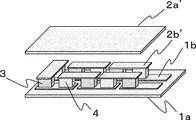
- the thermoelectric conversion module according to the embodiment of the present invention is configured as a so-called ⁇ -type thermoelectric conversion element, for example, a first substrate 1a having a first electrode 1b, a P-type thermoelectric element layer 3 and an N-type thermoelectric element. It includes a layer 4 and a second electrode 2b arranged to face the first electrode 1b, and further includes a second substrate 2a on the second electrode 2b.
- the area of the second electrode 2b is larger than the area of the first electrode 1b.
- a plurality of PN junction pairs in which the P-type thermoelectric element layer 3 and the N-type thermoelectric element layer 4 are PN-junctioned with the first electrode 1b or the second electrode 2b interposed therebetween are the first pair.
- the electrode 1 and the second electrode are alternately electrically connected in series and thermally connected in parallel.
- the PN junction pair composed of the P-type thermoelectric element layer 3 and the N-type thermoelectric element layer 4 is not particularly limited, and is usually a plurality of pairs, and can be appropriately adjusted and used.
- FIG. 2 is a perspective view for explaining an example of the configuration of a conventional thermoelectric conversion module.
- the conventional thermoelectric conversion module is configured as a ⁇ -type thermoelectric conversion element.
- a first substrate 1a having a first electrode 1b, a P-type thermoelectric element layer 3 and an N-type thermoelectric element layer 4, and the above-mentioned first.
- It includes a second electrode 2b'arranged so as to face the electrode 1b of 1, and further includes a second substrate 2a'on the second electrode 2b'.
- electrodes having approximately the same area are usually used.
- the surface of the first substrate 1a opposite to the first electrode 1b side is an endothermic surface, and the other surface, the second electrode 2b or the second substrate 2a.
- the surface opposite to the second electrode 2b side of the above can be used as the heat radiating surface.
- the object to be cooled is arranged on the endothermic surface and joined.
- the object to be cooled is not particularly limited, and examples thereof include an electronic element and the like. Among these, it is preferable to cool the electronic element from the viewpoint of efficient cooling in a short time.
- Examples of the electronic element include heat-generating electronic components such as a CPU, CMOS, a light emitting diode, a semiconductor laser, and a capacitor, and usually include those arranged in a mounting portion of a circuit board.
- the number of objects to be cooled is not particularly limited and may be a plurality.
- Examples of the method of joining with the object to be cooled include known methods such as bonding with an adhesive and soldering.
- the ratio R of the area of the second electrode to the area of the first electrode (hereinafter, the ratio R of the area of the second electrode to the area of the first electrode is referred to as "ratio R". )
- the ratio R depends on the electrode material used, but when the same electrode material is used, it is preferably 1.2 or more, and more preferably 1.5 ⁇ R ⁇ 100.0. It is more preferably 2.0 ⁇ R ⁇ 50.0, even more preferably 4.0 ⁇ R ⁇ 25.0, and particularly preferably 6.0 ⁇ R ⁇ 16.0.
- the ratio R is in this range, the heat dissipation property is improved, and the object to be cooled can reach and maintain a predetermined temperature in a shorter time.
- thermoelectric element layers such as the P-type thermoelectric element layer 3 and the N-type thermoelectric element layer 4 constituting the thermoelectric conversion module is not particularly limited, but from the viewpoint of increasing the area of the second electrode 2b, for example, As shown in FIG. 1, it is preferable to arrange them so as to have two rows and a plurality of columns. However, when the thermoelectric element layers are arranged in a plurality of rows and in a plurality of columns, the periphery of the plurality of thermoelectric element layers may be arranged so as to be surrounded by other adjacent thermoelectric element layers.
- thermoelectric element layer arranged in the second row in the center all the surroundings are surrounded by adjacent thermoelectric element layers, and the arrangement is physically close to each other. May become.
- the area of the second electrode 2b may be appropriately increased within a range in which the electrical connection and the thermal connection to the thermoelectric conversion module of the present invention are not impaired and the ratio R is satisfied. It is preferable to adjust it so that it becomes large.
- the total area of the joint surfaces of the P-type thermoelectric element layer 3 and the N-type thermoelectric element layer 4 with respect to the electrodes is not particularly limited, but is usually smaller than the area of the electrodes. Further, from the viewpoint of uniformity of performance balance and ease of manufacture of the PN junction pair, it is preferable to use the same size.
- the heat from the cooling object is the first.
- Heat is absorbed from the endothermic surface on the substrate 1a side, and heat is dissipated from the second substrate 2a side having the second electrode 2b. Since the area of the second electrode 2b is larger than the area of the first electrode 1b, heat is efficiently and sufficiently dissipated from the second substrate 2a.
- the thermoelectric conversion module having such a configuration can efficiently dissipate the heat generated by the object to be cooled.
- thermoelectric conversion module of the present invention it is preferable that the extending portion of the second electrode is thermally connected to a member made of a highly thermally conductive material.
- the extending portion means a region in which the second electrode extends in the horizontal direction.
- FIG. 3 is a transmission perspective view for explaining the configuration of the thermoelectric conversion module according to the second embodiment of the present invention (visualization of the component portion).
- the first substrate 1a having the first electrode 1b, the P-type thermoelectric element layer 3 and the N-type thermoelectric element layer 4 and a second electrode 2b arranged to face the first electrode 1b, and further include a second substrate 2a on the second electrode 2b.
- each electrode is further extended in the direction of a space portion not occupied by another thermoelectric element layer, and is thermally connected to a member 5 made of a highly thermally conductive material.
- the electrode 2b'' is arranged on the second substrate 2a using an electrode having the same specifications as the second electrode 2b from the viewpoint of heat dissipation.
- the highly thermally conductive material used for the member 5 examples include ceramic materials such as aluminum nitride, silicon nitride, and alumina having high insulating properties and thermal conductivity.
- the dimensions of the member 5 are not particularly limited as long as the heat dissipation can be maintained.
- the heat from the cooling object is the first.
- the heat is absorbed from the endothermic surface on the substrate 1a side, and is dissipated from the second substrate 2a side having the second electrode 2b and the electrode 2b ′′, and is stored in the member 5 and dissipated. Since the area of the second electrode 2b (including the electrode 2b'') is larger than the area of the first electrode 1b and further includes the member 5, heat is dissipated more efficiently, quickly and sufficiently than in the first embodiment. Will be done. With the thermoelectric conversion module having such a configuration, the heat generated by the object to be cooled can be dissipated more efficiently.
- the second substrate has through holes, and the second electrodes are formed on both sides of the second substrate with the through holes interposed therebetween, and are electrically and electrically. It is preferably thermally connected. Further, the P-type thermoelectric element layer and the other electrode surface side of the second electrode opposite to one electrode surface side of the P-type thermoelectric element layer and the N-type thermoelectric element layer side are the P-type of the second substrate. It is preferable that the thermoelectric element layer extends on the second substrate on the side opposite to the N-type thermoelectric element layer side and is arranged as a continuous layer. Further, one of the electrode surface sides of the second electrode, which is the P-type thermoelectric element layer and the N-type thermoelectric element layer side, extends on the second substrate through the opening end of the through hole. It may be arranged as a continuous layer.
- FIG. 4 is a cross-sectional view showing the configuration of the thermoelectric conversion module according to the third embodiment of the present invention.
- the thermoelectric conversion module according to the third embodiment of the present invention includes a first substrate 11a having a first electrode 11b, a P-type thermoelectric element layer 13 and an N-type thermoelectric element layer 14, and the first electrode 11b. It includes a second electrode 12b arranged so as to face each other and a second substrate 12a.
- the second electrode 12b is formed on both sides of the second substrate 12a with through holes 17 interposed therebetween and is electrically and thermally connected.
- the second electrode 12b on the P-type thermoelectric element layer 13 and N-type thermoelectric element layer 14 side and the other electrode surface side of the second electrode 12b on the opposite side are the first. It extends on the substrate 12a of No. 2 and is arranged as a continuous layer. The area of the second electrode 12b having a continuous layer provided on the second substrate 12a can be further expanded. It is preferable that the second electrode 12b is appropriately adjusted within a range in which the electrical connection and the thermal connection to the thermoelectric element layer are not impaired and the ratio R is satisfied (not shown).
- the cooling object 16 is thermally connected to, for example, the first substrate 11a side.
- the through holes 17 can be formed by a known method. For example, it can be formed by drilling or plating. The through hole 17 may be filled with a metal material or the like. The filling improves the heat exhaust efficiency.
- the heat from the electronic element is generated by the first substrate by arranging the electronic element as the cooling object 16 with the side of the first substrate 11a having the first electrode 11b as the endothermic surface. Heat is absorbed from the endothermic surface on the 11a side, and heat is dissipated from the second electrode 12b. Since the second electrode 12b extends through the through hole 17 of the second substrate 12a and the front surface is enlarged and arranged as a continuous layer on the back surface side, efficient heat dissipation is performed quickly and sufficiently. With the thermoelectric conversion module having such a configuration, the heat generated by the electronic element as the cooling object 16 can be dissipated more efficiently.
- thermoelectric conversion module In the configuration of the thermoelectric conversion module of the present invention, the thermoelectric conversion module is arranged inside the through hole of the second substrate, and the second electrode of the thermoelectric conversion module extends on the second substrate. It is preferable that the layers are arranged as a continuous layer.
- FIG. 5 is a cross-sectional view showing the configuration of the thermoelectric conversion module according to the fourth embodiment of the present invention.
- the first electrode 11b, the P-type thermoelectric element layer 13 and the N-type thermoelectric element layer 14, and the first electrode 11b are arranged to face each other. 2 electrodes 12b and 2 are included.
- the P-type thermoelectric element layer 13 and the N-type thermoelectric element layer 14 are arranged inside the second substrate 12a, and the second electrode 12b extends to the back surface side of the second substrate 12a and is continuous. Arranged as a layer.
- the second electrode 12b is appropriately adjusted within a range in which the electrical connection and the thermal connection to the thermoelectric element layer are not impaired and the ratio R is satisfied (not shown).
- the object to be cooled 16 is thermally connected to, for example, the first electrode 11b.
- the heat from the electronic element is flush with the second substrate 12a.
- Heat is absorbed from the endothermic surface on the side of the first electrode 11b, and heat is dissipated from the second electrode 12b.
- the second electrode 12b is expanded and arranged as a continuous layer on the back surface side of the second substrate 12a, heat dissipation is efficiently and sufficiently performed.
- the thermoelectric conversion module having such a configuration, the heat generated by the electronic element as the cooling object 16 can be dissipated more efficiently.
- the P-type thermoelectric element layer and the N-type thermoelectric element layer used in the present invention are not particularly limited, but consist of a thermoelectric semiconductor material, a heat-resistant resin, and a thermoelectric semiconductor composition containing an ionic liquid and / or an inorganic ionic compound. Is preferable.
- thermoelectric semiconductor material used for the thermoelectric element layer is preferably pulverized to a predetermined size by, for example, a fine pulverizer or the like and used as thermoelectric semiconductor particles (hereinafter, the thermoelectric semiconductor material may be referred to as "thermoelectric semiconductor particles"). .).
- the particle size of the thermoelectric semiconductor particles is preferably 10 nm to 100 ⁇ m, more preferably 20 nm to 50 ⁇ m, and even more preferably 30 nm to 30 ⁇ m.
- the average particle size of the thermoelectric semiconductor fine particles was obtained by measuring with a laser diffraction type particle size analyzer (Mastersizer 3000 manufactured by Malvern), and was used as the median value of the particle size distribution.
- thermoelectric semiconductor material constituting the P-type thermoelectric element layer and the N-type thermoelectric element layer is any material that can generate a thermoelectric force by imparting a temperature difference.
- the present invention is not particularly limited, and for example, a bismuth-tellu thermoelectric semiconductor material such as P-type bismasterlide and N-type bismasterlide; a telluride thermoelectric semiconductor material such as GeTe and PbTe; an antimony-tellu thermoelectric semiconductor material; ZnSb, Zn 3 Sb.
- Zinc-antimon thermoelectric semiconductor materials such as 2, Zn 4 Sb 3 ; silicon-germanium thermoelectric semiconductor materials such as SiGe; bismus selenide thermoelectric semiconductor materials such as Bi 2 Se 3 ; ⁇ -FeSi 2 , CrSi 2, MnSi VDD-based thermoelectric semiconductor materials such as 1.73 and Mg 2 Si; oxide-based thermoelectric semiconductor materials; Whistler materials such as FeVAL, FeVALSi, and FeVTiAl, and sulfide-based thermoelectric semiconductor materials such as TiS 2 are used.
- thermoelectric semiconductor material used in the present invention is preferably a bismuth-tellurium-based thermoelectric semiconductor material such as P-type bismuthellide or N-type bismuthellide.
- P-type bismuth telluride one having a hole as a carrier and a positive Seebeck coefficient, for example, represented by Bi X Te 3 Sb 2-X is preferably used.
- X is preferably 0 ⁇ X ⁇ 0.8, more preferably 0.4 ⁇ X ⁇ 0.6.
- X is larger than 0 and 0.8 or less, the Seebeck coefficient and the electric conductivity become large, and the characteristics as a P-type thermoelectric conversion material are maintained, which is preferable.
- N-type bismuth telluride one having an electron carrier and a negative Seebeck coefficient, for example, represented by Bi 2 Te 3-Y Se Y is preferably used.
- the Seebeck coefficient and the electric conductivity become large, and the characteristics as an N-type thermoelectric conversion material are maintained, which is preferable.
- the blending amount of the thermoelectric semiconductor particles in the thermoelectric semiconductor composition is preferably 30 to 99% by mass. It is more preferably 50 to 96% by mass, and even more preferably 70 to 95% by mass.
- the Seebeck coefficient absolute value of the Perche coefficient
- the decrease in the electric conductivity is suppressed, and only the thermal conductivity is decreased, so that high thermoelectric performance is exhibited.
- a film having sufficient film strength and flexibility can be obtained, which is preferable.
- thermoelectric semiconductor particles are annealed (hereinafter, may be referred to as "annealing treatment A").
- annealing treatment A By performing the annealing treatment A, the crystallinity of the thermoelectric semiconductor particles is improved, and the surface oxide film of the thermoelectric semiconductor particles is removed, so that the Seebeck coefficient (absolute value of the Perche coefficient) of the thermoelectric conversion material is increased. , The thermoelectric performance index can be further improved.
- the heat-resistant resin used in the present invention acts as a binder between thermoelectric semiconductor particles and enhances the flexibility of the thermoelectric element layer.
- the heat-resistant resin is not particularly limited, but when a thin film made of a thermoelectric semiconductor composition is subjected to crystal growth of thermoelectric semiconductor particles by annealing or the like, various factors such as mechanical strength and thermal conductivity as a resin are obtained. Use a heat-resistant resin that maintains its physical properties without being impaired.
- the heat-resistant resin include polyamide resins, polyamideimide resins, polyimide resins, polyetherimide resins, polybenzoxazole resins, polybenzoimidazole resins, epoxy resins, and copolymers having a chemical structure of these resins.
- the heat-resistant resin may be used alone or in combination of two or more.
- polyamide resins, polyamide-imide resins, polyimide resins, and epoxy resins are preferable and have excellent flexibility because they have higher heat resistance and do not adversely affect the crystal growth of thermoelectric semiconductor particles in the thin film. Therefore, polyamide resin, polyamide-imide resin, and polyimide resin are more preferable.
- the polyimide resin is more preferable as the heat-resistant resin from the viewpoint of adhesion to the polyimide film and the like.
- the polyimide resin is a general term for polyimide and its precursor.
- the heat-resistant resin preferably has a decomposition temperature of 300 ° C. or higher.
- the decomposition temperature is within the above range, the flexibility of the thermoelectric element layer can be maintained without losing the function as a binder even when the thin film made of the thermoelectric semiconductor composition is annealed, as will be described later.
- the blending amount of the heat-resistant resin in the thermoelectric semiconductor composition is preferably 0.1 to 40% by mass, more preferably 0.5 to 20% by mass, and further preferably 1 to 20% by mass.
- a film having both high thermoelectric performance and film strength can be obtained.
- the ionic liquid that can be contained in the thermoelectric semiconductor composition is a molten salt formed by combining a cation and an anion, and refers to a salt that can exist as a liquid in any temperature range of ⁇ 50 ° C. or higher and lower than 400 ° C.
- the ionic liquid is an ionic compound having a melting point in the range of ⁇ 50 ° C. or higher and lower than 400 ° C.
- the melting point of the ionic liquid is preferably ⁇ 25 ° C. or higher and 200 ° C. or lower, and more preferably 0 ° C. or higher and 150 ° C. or lower.
- Ionic liquids have features such as extremely low vapor pressure, non-volatility, excellent thermostability and electrochemical stability, low viscosity, and high ionic conductivity. Therefore, as a conductive auxiliary agent, it is possible to effectively suppress a decrease in electrical conductivity between thermoelectric semiconductor materials. Further, since the ionic liquid exhibits high polarity based on the aprotic ionic structure and has excellent compatibility with the heat-resistant resin, the electric conductivity of the thermoelectric conversion material can be made uniform.
- ionic liquid known or commercially available ones can be used.
- nitrogen-containing cyclic cation compounds such as pyridinium, pyrimidinium, pyrazolium, pyrrolidinium, piperidinium, imidazolium and their derivatives; tetraalkylammonium-based amine-based cations and their derivatives; phosphonium, trialkylsulfonium, tetraalkylphosphonium and the like.
- phosphine cations and derivatives thereof and a cationic component such as lithium cations and derivatives thereof, Cl -, Br -, I -, AlCl 4 -, Al 2 Cl 7 -, BF 4 -, PF 6 -, ClO 4 -, NO 3 -, CH 3 COO - , CF 3 COO -, CH 3 SO 3 -, CF 3 SO 3 -, (FSO 2) 2 N -, (CF 3 SO 2) 2 N -, (CF 3 SO 2) 3 C -, AsF 6 -, SbF 6 -, NbF 6 -, TaF 6 -, F (HF) n -, (CN) 2 n -, C 4 F 9 SO 3 -, (C 2 F 5 SO 2) Examples thereof include those composed of anionic components such as 2 N ⁇ , C 3 F 7 COO ⁇ , and (CF 3 SO 2 ) (CF 3 CO) N ⁇ .
- the cation component of the ionic liquid is a pyridinium cation and its derivatives from the viewpoints of high temperature stability, compatibility with thermoelectric semiconductor materials and resins, and suppression of decrease in electrical conductivity between thermoelectric semiconductor material gaps.
- 1-butyl-4-methylpyridinium bromide, 1-butylpyridinium bromide, and 1-butyl-4-methylpyridinium hexafluorophosphate are preferable.
- the cation component is [1-butyl-3- (2-hydroxyethyl) imidazolium bromide], [1-butyl-3- (2-hydroxyethyl) imidazole].
- Rium tetrafluoroborate] is preferable.
- the above-mentioned ionic liquid preferably has a decomposition temperature of 300 ° C. or higher. As long as the decomposition temperature is within the above range, the effect as a conductive auxiliary agent can be maintained even when the thin film made of the thermoelectric semiconductor composition is annealed, as will be described later.
- the blending amount of the ionic liquid in the thermoelectric semiconductor composition is preferably 0.01 to 50% by mass, more preferably 0.5 to 30% by mass, and further preferably 1.0 to 20% by mass.
- the blending amount of the ionic liquid is within the above range, the decrease in electrical conductivity is effectively suppressed, and a film having high thermoelectric performance can be obtained.
- the inorganic ionic compound that can be contained in the thermoelectric semiconductor composition is a compound composed of at least cations and anions. Since the inorganic ionic compound exists as a solid in a wide temperature range of 400 to 900 ° C. and has characteristics such as high ionic conductivity, it can be used as a conductivity auxiliary agent to reduce the electrical conductivity between thermoelectric semiconductor materials. Can be suppressed.
- the blending amount of the inorganic ionic compound in the thermoelectric semiconductor composition is preferably 0.01 to 50% by mass, more preferably 0.5 to 30% by mass, and further preferably 1.0 to 10% by mass.
- the blending amount of the inorganic ionic compound is within the above range, the decrease in electrical conductivity can be effectively suppressed, and as a result, a film having improved thermoelectric performance can be obtained.
- the total content of the inorganic ionic compound and the ionic liquid in the thermoelectric semiconductor composition is preferably 0.01 to 50% by mass, more preferably. Is 0.5 to 30% by mass, more preferably 1.0 to 10% by mass.
- thermoelectric element layer made of the thermoelectric semiconductor composition can be formed, for example, by applying the thermoelectric semiconductor composition on a substrate and drying it. By forming in this way, a large number of thermoelectric conversion element layers can be easily obtained at low cost.
- a method of applying a thermoelectric semiconductor composition to obtain a thermoelectric element layer a screen printing method, a flexographic printing method, a gravure printing method, a spin coating method, a dip coating method, a die coating method, a spray coating method, a bar coating method, and a doctor blade
- Known methods such as a method can be mentioned and are not particularly limited.
- thermoelectric element layer When the coating film is formed into a pattern, a screen printing method, a slot die coating method, or the like, which enables easy pattern formation using a screen plate having a desired pattern, is preferably used. Then, the obtained coating film is dried to form a thermoelectric element layer.
- the thickness of the thermoelectric element layer is not particularly limited, and is preferably 100 nm to 1000 ⁇ m, more preferably 300 nm to 600 ⁇ m, and further preferably 5 to 400 ⁇ m from the viewpoint of thermoelectric performance and film strength.
- the P-type thermoelectric element layer and the N-type thermoelectric element layer as a thin film made of the thermoelectric semiconductor composition are further subjected to an annealing treatment (hereinafter, may be referred to as "annealing treatment B").
- annealing treatment B By performing the annealing treatment B, the thermoelectric performance can be stabilized, and the thermoelectric semiconductor particles in the thin film can be crystal-grown, so that the thermoelectric performance can be further improved.
- the annealing treatment B is not particularly limited, but is usually carried out under an inert gas atmosphere such as nitrogen or argon, a reducing gas atmosphere, or a vacuum condition in which the gas flow rate is controlled, and the resin and the ionic compound to be used are used. Although it depends on the heat-resistant temperature and the like, it is carried out at 100 to 500 ° C. for several minutes to several tens of hours.
- the first substrate and the second substrate used in the thermoelectric conversion module of the present invention are not particularly limited, and are independently a paper phenol substrate, a paper epoxy substrate, a glass composite substrate, a glass epoxy substrate, a glass polyimide substrate, and fluorine.
- a substrate, a glass PPO substrate, glass, ceramics, a plastic film, or the like can be used.
- a plastic film is preferable from the viewpoint of having flexibility and having a degree of freedom for installation of a heat source on the surface.
- polyimide film polyamide film, polyetherimide film, polyaramid film, polyamideimide film, polysulfon film, glass composite substrate, glass epoxy substrate, and glass polyimide substrate are available.
- a polyimide film, a paper phenol substrate, a paper epoxy substrate, a glass composite substrate, a glass epoxy substrate, and a glass polyimide substrate are particularly preferable.
- the thickness of the first substrate and the second substrate are independently, preferably 1 to 1000 ⁇ m, more preferably 10 to 500 ⁇ m, and even more preferably 20 to 100 ⁇ m from the viewpoint of heat resistance and flexibility.
- the metal materials used for the first electrode and the second electrode are not particularly limited, but are independently copper, gold, nickel, aluminum, rhodium, platinum, chromium, palladium, and stainless steel, respectively. Alloys containing steel, molybdenum or any of these metals are preferred. Further, not only a single layer but also a plurality of layers may be combined to form a multi-layer structure.
- the thickness of the layers of the first electrode and the second electrode are independently, preferably 10 nm to 200 ⁇ m, more preferably 30 nm to 150 ⁇ m, and further preferably 50 nm to 120 ⁇ m. When the thickness of the layers of the first electrode and the second electrode is within the above range, the electrical conductivity is high and the resistance is low, and sufficient strength as an electrode can be obtained.
- the formation of the first electrode and the second electrode is performed using the metal material described above.
- a method of forming the first electrode and the second electrode after providing an electrode having no pattern formed on the substrate, a known physical treatment or chemical treatment mainly composed of a photolithography method, or a method thereof.
- a method of processing into a predetermined pattern shape by using the above in combination, or a method of directly forming an electrode pattern by a screen printing method, an inkjet method, or the like can be mentioned.
- PVD Physical Vapor Deposition Method
- CVD Chemical Vapor Deposition
- thermal CVD thermal CVD
- atomic layer deposition ALD
- various coating methods such as dip coating method, spin coating method, spray coating method, gravure coating method, die coating method, doctor blade method, wet process such as electrodeposition method, silver salt method .
- Electrolytic plating method, electroless plating method, lamination of metal foil and the like are appropriately selected according to the material of the electrode. From the viewpoint of thermoelectric performance, high conductivity and high thermal conductivity are required, so it is preferable to use an electrode formed by a plating method or a vacuum film forming method.
- a laminating agent is used to bond the P-type thermoelectric element layer and the N-type thermoelectric element layer to the electrodes.
- the bonding agent include a conductive paste and the like.
- the conductive paste include copper paste, silver paste, nickel paste and the like, and when a binder is used, epoxy resin, acrylic resin, urethane resin and the like can be mentioned.
- the method of applying the bonding agent on the electrodes of the substrate include known methods such as a screen printing method and a dispensing method.
- solder material can be used for bonding with the electrode.
- the solder material may be appropriately selected, and Sn, Sn / Pb alloy, Sn / Ag alloy, Sn / Cu alloy, Sn / Sb alloy, Sn / In alloy, Sn / Zn alloy, Sn / In / Bi alloy, etc.
- Known materials such as Sn / In / Bi / Zn alloys and Sn / Bi / Pb / Cd alloys can be mentioned.
- Examples of the method of applying the solder material onto the electrodes of the substrate include known methods such as a screen printing method and a dispensing method.
- thermoelectric conversion module of the present invention has been described above, the present invention is not limited to the above embodiment and can be further modified in various ways.
- thermoelectric conversion module of the present invention a thermoelectric conversion module having further improved heat dissipation can be obtained with a simple configuration in which the area of the second electrode is made larger than the area of the first electrode.
- thermoelectric conversion module of the present invention is a thermoelectric conversion module composed of a ⁇ -type thermoelectric conversion element and having a simple configuration in which the area of the second electrode is larger than the area of the first electrode to further improve heat dissipation. Therefore, it is conceivable to apply it mainly in the field of electronic equipment described above as a cooling application. In addition, it is attached to the neck and arm for power generation applications that convert exhaust heat from various combustion furnaces such as factories, waste combustion furnaces, cement combustion furnaces, automobile combustion gas exhaust heat, and electronic equipment exhaust heat into electricity. It can also be applied to power generation applications that utilize the temperature difference between the human body temperature and the outside air.
- thermoelectric element layer 4 N-type thermoelectric element layer 5: Member 11a : First substrate 11b: First electrode 12b, 12b': Second electrode 13: P-type thermoelectric element layer 13: N-type thermoelectric element layer 15: Heat dissipation substrate 16: Cooling object 17: Through hole
Abstract
Provided is a thermoelectric conversion module of which heat dissipation property is further improved by a simple configuration. The thermoelectric conversion module comprises a first electrode, a P-type thermoelectric element layer and an N-type thermoelectric element layer, and a second electrode opposing the first electrode. A plurality of PN junction pairs each comprising a PN junction of the P-type thermoelectric element layer and the N-type thermoelectric element layer with the first electrode or the second electrode interposed therebetween are electrically connected in series alternately by the first electrode and the second electrode. In the thermoelectric conversion module, the area of the second electrode is greater than the area of the first electrode.
Description
本発明は、熱電変換モジュールに関する。
The present invention relates to a thermoelectric conversion module.
従来から、ゼーベック効果やペルチェ効果などの熱電効果を有する熱電変換材料を用い、熱エネルギーと電気エネルギーとを相互変換するようにした熱電変換モジュールがある。
前記熱電変換モジュールとして、いわゆるπ型の熱電変換素子の構成が知られている。π型は、例えば、互いに離間するー対の電極を基板上に設け、―方の電極の上にP型熱電素子の下面を、他方の電極の上にN型熱電素子の下面を、同じく互いに離間して設け、P型熱電素子及びN型熱電素子の反対側のそれぞれの上面を対向する基板の電極に接合(以下、「PN接合」ということがある。)することで構成される。通常は、熱電性能の観点から、PN接合した一対のP型熱電素子とN型熱電素子とが複数対用いられ、電気的には直列接続、熱的には並列接続するように構成される。 Conventionally, there is a thermoelectric conversion module that uses a thermoelectric conversion material having a thermoelectric effect such as the Seebeck effect and the Perche effect to convert between thermal energy and electrical energy.
As the thermoelectric conversion module, a configuration of a so-called π-type thermoelectric conversion element is known. In the π-type, for example, a pair of electrodes that are separated from each other are provided on the substrate, and the lower surface of the P-type thermoelectric element is provided on the one electrode and the lower surface of the N-type thermoelectric element is provided on the other electrode. The P-type thermoelectric element and the N-type thermoelectric element are provided apart from each other, and the upper surfaces of the P-type thermoelectric elements and the N-type thermoelectric elements are bonded to the electrodes of the opposing substrates (hereinafter, may be referred to as “PN junction”). Usually, from the viewpoint of thermoelectric performance, a plurality of pairs of PN-junctioned P-type thermoelectric elements and N-type thermoelectric elements are used, and are configured to be electrically connected in series and thermally connected in parallel.
近年、コンピューター、ミラーレスカメラ、また、スマートフォン等の携帯端末等のエレクトロニクス機器には、それらの動作や制御を行うCPU(Central Processing Unit)、CMOS(Complementary Metal Oxide Semiconductor)、発光ダイオード等の半導体素子に代表される電子素子が基板に高密度に実装されることが当たり前のものとなっており、さらに微細化による半導体素子のさらなる小型化、高性能化等に伴い、半導体素子自体が高温になりかつ多量の熱を放出する発熱体となってきている。このような状況下、当該半導体素子等の発熱をさらに効率良く吸熱、放熱する冷却デバイスが求められている。
その対応方法の一つとして、前記熱電変換モジュールを用いた電子冷却等が用いられる。
特許文献1には、基板上の電子素子の表面に吸熱面が接合された冷却素子としてペルチェ素子を用い、さらに冷却素子の放熱面の側に接続されて電子素子からの熱が放熱される、前記冷却素子の放熱面の面積よりも大きく前記基板の表面積以下の面を有する金属製の板材と、前記冷却素子の放熱面の面積よりも大きく前記基板の表面積以下の面を有する熱伝導シートであって、―方の面が前記板材に接合され他方の面が前記冷却素子の放熱面に接合される熱伝導シートと、を含む、台座を備えた放熱構造を開示している。 In recent years, electronic devices such as computers, mirrorless cameras, and mobile terminals such as smartphones have semiconductor elements such as CPUs (Central Processing Units), CMOSs (Complementary Metal Oxide Semiconductors), and light emitting diodes that operate and control them. It has become commonplace for electronic devices represented by Moreover, it has become a heating element that releases a large amount of heat. Under such circumstances, there is a demand for a cooling device that more efficiently absorbs and dissipates heat generated by the semiconductor element or the like.
As one of the corresponding methods, electronic cooling or the like using the thermoelectric conversion module is used.
InPatent Document 1, a Pelche element is used as a cooling element in which a heat absorbing surface is bonded to the surface of the electronic element on the substrate, and further connected to the heat radiating surface side of the cooling element to dissipate heat from the electronic element. A metal plate having a surface area larger than the surface area of the cooling element and less than the surface area of the substrate, and a heat conductive sheet having a surface area larger than the surface area of the heat radiating surface of the cooling element and less than the surface area of the substrate. There is disclosed a heat dissipation structure with a pedestal, including a heat conductive sheet in which one side is joined to the plate material and the other side is joined to the heat dissipation surface of the cooling element.
その対応方法の一つとして、前記熱電変換モジュールを用いた電子冷却等が用いられる。
特許文献1には、基板上の電子素子の表面に吸熱面が接合された冷却素子としてペルチェ素子を用い、さらに冷却素子の放熱面の側に接続されて電子素子からの熱が放熱される、前記冷却素子の放熱面の面積よりも大きく前記基板の表面積以下の面を有する金属製の板材と、前記冷却素子の放熱面の面積よりも大きく前記基板の表面積以下の面を有する熱伝導シートであって、―方の面が前記板材に接合され他方の面が前記冷却素子の放熱面に接合される熱伝導シートと、を含む、台座を備えた放熱構造を開示している。 In recent years, electronic devices such as computers, mirrorless cameras, and mobile terminals such as smartphones have semiconductor elements such as CPUs (Central Processing Units), CMOSs (Complementary Metal Oxide Semiconductors), and light emitting diodes that operate and control them. It has become commonplace for electronic devices represented by Moreover, it has become a heating element that releases a large amount of heat. Under such circumstances, there is a demand for a cooling device that more efficiently absorbs and dissipates heat generated by the semiconductor element or the like.
As one of the corresponding methods, electronic cooling or the like using the thermoelectric conversion module is used.
In
しかしながら、特許文献1においては、基板上の電子素子からの熱を放熱する構造が、冷却素子として用いるペルチェ素子の放熱面に、金属製の板材と熱伝導シートとを接合した台座をさらに熱的に接続したものであり、しかも、熱伝導シートとしては、例えば、グラファイトシートを両側から挟み込む一対の伝熱性金属板を使用するため、構成が複雑となり、製造プロセスの追加、実装の煩雑性及び材料コスト増大等の観点から問題となることがある。
However, in Patent Document 1, the structure that dissipates heat from the electronic element on the substrate further heats the pedestal in which the metal plate material and the heat conductive sheet are joined to the heat radiating surface of the Pelche element used as the cooling element. As the heat conductive sheet, for example, a pair of heat conductive metal plates sandwiching a graphite sheet from both sides are used, which complicates the configuration, adds a manufacturing process, complicates mounting, and materials. It may be a problem from the viewpoint of cost increase.
本発明は、上記を鑑み、簡易な構成で放熱性がさらに向上した熱電変換モジュールを提供することを課題とする。
In view of the above, it is an object of the present invention to provide a thermoelectric conversion module having a simple configuration and further improved heat dissipation.
本発明者らは、上記課題を解決すべく鋭意検討を重ねた結果、熱電変換モジュールを構成するP型熱電素子及びN型熱電素子のPN接合対の形成に用いる第2の電極の面積を、対向するPN接合対の形成に用いる第1の電極の面積より大きくすることにより、第2の電極の面からの放熱性がさらに向上することを見出し、本発明を完成した。
すなわち、本発明は、以下の(1)~(6)を提供するものである。
(1)第1の電極と、P型熱電素子層及びN型熱電素子層と、前記第1の電極に対向して配置された第2の電極と、を含み、前記P型熱電素子層と前記N型熱電素子層とが前記第1の電極又は前記第2の電極を介在しPN接合されたPN接合対が複数対、前記第1の電極と前記第2の電極とで交互に電気的に直列接続された熱電変換モジュールであって、前記第2の電極の面積が、前記第1の電極の面積より大きい、熱電変換モジュール。
(2)前記第1の電極の面積に対する前記第2の電極の面積の比率Rが、1.20以上である、上記(1)に記載の熱電変換モジュール。
(3)さらに第1の基板及び/又は第2の基板を含む、上記(1)又は(2)に記載の熱電変換モジュール。
(4)前記第2の電極の延在部が高熱伝導性材料からなる部材と熱的に接続される、上記(1)~(3)のいずれかに記載の熱電変換モジュール。
(5)前記第2の基板はスルーホールを有し、前記第2の電極は、前記第2の基板の両面に前記スルーホールを介在して形成され、前記第2の電極の、前記P型熱電素子層及びN型熱電素子層側の一方の電極面側とは反対側の他方の電極面側は、前記第2の基板の、前記P型熱電素子層及びN型熱電素子層側とは反対側の第2の基板上に延在し、連続層として配置される、上記(1)~(4)のいずれかに記載の熱電変換モジュール。
(6)前記熱電変換モジュールが前記第2の基板の前記スルーホールの内部に配置され、かつ前記熱電変換モジュールの前記第2の電極が、前記第2の基板上に前記スルーホールを介在し延在し、連続層として配置される、上記(1)~(5)のいずれかに記載の熱電変換モジュール。 As a result of diligent studies to solve the above problems, the present inventors have determined the area of the second electrode used for forming the PN junction pair of the P-type thermoelectric element and the N-type thermoelectric element constituting the thermoelectric conversion module. The present invention has been completed by finding that the heat dissipation from the surface of the second electrode is further improved by making the area larger than the area of the first electrode used for forming the opposing PN junction pair.
That is, the present invention provides the following (1) to (6).
(1) The P-type thermoelectric element layer includes a first electrode, a P-type thermoelectric element layer, an N-type thermoelectric element layer, and a second electrode arranged so as to face the first electrode. A plurality of pairs of PN junctions in which the N-type thermoelectric element layer is PN-bonded with the first electrode or the second electrode interposed therebetween, and the first electrode and the second electrode are alternately electrically connected. A thermoelectric conversion module connected in series to the above, wherein the area of the second electrode is larger than the area of the first electrode.
(2) The thermoelectric conversion module according to (1) above, wherein the ratio R of the area of the second electrode to the area of the first electrode is 1.20 or more.
(3) The thermoelectric conversion module according to (1) or (2) above, further including a first substrate and / or a second substrate.
(4) The thermoelectric conversion module according to any one of (1) to (3) above, wherein the extending portion of the second electrode is thermally connected to a member made of a highly thermally conductive material.
(5) The second substrate has a through hole, and the second electrode is formed with the through hole interposed therebetween on both sides of the second substrate, and the P-type of the second electrode. The thermoelectric element layer and the other electrode surface side opposite to one electrode surface side on the N-type thermoelectric element layer side are the P-type thermoelectric element layer and the N-type thermoelectric element layer side of the second substrate. The thermoelectric conversion module according to any one of (1) to (4) above, which extends on a second substrate on the opposite side and is arranged as a continuous layer.
(6) The thermoelectric conversion module is arranged inside the through hole of the second substrate, and the second electrode of the thermoelectric conversion module extends on the second substrate with the through hole interposed therebetween. The thermoelectric conversion module according to any one of (1) to (5) above, which is present and arranged as a continuous layer.
本発明によれば、簡易な構成で放熱性がさらに向上した熱電変換モジュールを提供することができる。
According to the present invention, it is possible to provide a thermoelectric conversion module having further improved heat dissipation with a simple configuration.
[熱電変換モジュール]
本発明の熱電変換モジュールは、第1の電極と、P型熱電素子層及びN型熱電素子層と、前記第1の電極に対向して配置された第2の電極と、を含み、前記P型熱電素子層と前記N型熱電素子層とが前記第1の電極又は前記第2の電極を介在しPN接合されたPN接合対が複数対、前記第1の電極と前記第2の電極とで交互に電気的に直列接続された熱電変換モジュールであって、前記第2の電極の面積が、前記第1の電極の面積より大きい、ことを特徴とする。
本発明の熱電変換モジュールでは、該熱電変換モジュールを構成する第2の電極の面積を第1の電極の面積より大きくすることにより、例えば、第1の電極側を吸熱面となるよう冷却対象物を配置した後、熱電変換モジュールを通電した場合に、該冷却対象物から発生した熱を第2の電極から効率的に放熱することができる。
なお、熱電変換素子は、通常、吸熱側と放熱側の位置関係は、通電の方向により逆転する。また、吸熱側と放熱側が入れ替わることにより、出力の極性が入れ替わる。このようなことから、どちらの電極が吸熱側、放熱側であるかについては本発明を制限するものではない。本明細書では、便宜的に第2の電極側を放熱側、第1の電極側を吸熱側として記載した。 [Thermoelectric conversion module]
The thermoelectric conversion module of the present invention includes a first electrode, a P-type thermoelectric element layer and an N-type thermoelectric element layer, and a second electrode arranged to face the first electrode, and the P A plurality of pairs of PN junctions in which the type thermoelectric element layer and the N-type thermoelectric element layer are PN-bonded with the first electrode or the second electrode interposed therebetween, the first electrode and the second electrode. It is a thermoelectric conversion module electrically connected in series alternately, wherein the area of the second electrode is larger than the area of the first electrode.
In the thermoelectric conversion module of the present invention, by making the area of the second electrode constituting the thermoelectric conversion module larger than the area of the first electrode, for example, the object to be cooled so that the first electrode side becomes an endothermic surface. When the thermoelectric conversion module is energized after arranging the above, the heat generated from the object to be cooled can be efficiently dissipated from the second electrode.
In the thermoelectric conversion element, the positional relationship between the endothermic side and the heat radiating side is usually reversed depending on the direction of energization. Further, the polarity of the output is switched by switching the endothermic side and the heat radiating side. Therefore, the present invention is not limited as to which electrode is on the endothermic side or the heat radiating side. In this specification, for convenience, the second electrode side is described as the heat dissipation side, and the first electrode side is described as the endothermic side.
以下、本発明を図を用い、実施形態により具体的に説明する。
Hereinafter, the present invention will be specifically described with reference to the drawings.
(第1実施形態)
本発明の熱電変換モジュールの構成において、さらに第1の基板及び/又は第2の基板を含むことが好ましい。例えば、第2の基板を設けることにより、第2の電極で生じる放熱分布が均一化され放熱性がさらに向上する。 (First Embodiment)
In the configuration of the thermoelectric conversion module of the present invention, it is preferable to further include a first substrate and / or a second substrate. For example, by providing the second substrate, the heat dissipation distribution generated by the second electrode is made uniform, and the heat dissipation property is further improved.
図1は本発明の第1実施形態に係る熱電変換モジュールの構成を説明するための透過斜視図(構成部を可視化)であり、(a)が第2の電極の配置の態様を示す透過斜視図であり、(b)が熱電変換モジュールの全体の構成を示す透過斜視図である。
本発明の実施形態に係る熱電変換モジュールは、いわゆるπ型の熱電変換素子として構成され、例えば、第1の電極1bを有する第1の基板1aと、P型熱電素子層3及びN型熱電素子層4と、前記第1の電極1bに対向して配置された第2の電極2bと、を含み、さらに第2の基板2aを第2の電極2b上に含む。
互いに対向する第1の電極1bの面積と第2の電極2bの面積にあっては、第2の電極2bの面積が、第1の電極1bの面積より大きい。
また、図1において、P型熱電素子層3とN型熱電素子層4とが前記第1の電極1b又は前記第2の電極2bを介在しPN接合されたPN接合対が複数対、前記第1の電極と前記第2の電極とで交互に電気的に直列接続に、また熱的には並列接続される。P型熱電素子層3及びN型熱電素子層4からなるPN接合対は、特に制限されず、通常複数対であり、適宜調整され用いることができる。 FIG. 1 is a transmission perspective view (visualizing a component portion) for explaining the configuration of the thermoelectric conversion module according to the first embodiment of the present invention, and FIG. 1A is a transmission perspective view showing an aspect of arrangement of a second electrode. It is a figure, (b) is a transmission perspective view which shows the whole structure of a thermoelectric conversion module.
The thermoelectric conversion module according to the embodiment of the present invention is configured as a so-called π-type thermoelectric conversion element, for example, afirst substrate 1a having a first electrode 1b, a P-type thermoelectric element layer 3 and an N-type thermoelectric element. It includes a layer 4 and a second electrode 2b arranged to face the first electrode 1b, and further includes a second substrate 2a on the second electrode 2b.
In the area of thefirst electrode 1b and the area of the second electrode 2b facing each other, the area of the second electrode 2b is larger than the area of the first electrode 1b.
Further, in FIG. 1, a plurality of PN junction pairs in which the P-typethermoelectric element layer 3 and the N-type thermoelectric element layer 4 are PN-junctioned with the first electrode 1b or the second electrode 2b interposed therebetween are the first pair. The electrode 1 and the second electrode are alternately electrically connected in series and thermally connected in parallel. The PN junction pair composed of the P-type thermoelectric element layer 3 and the N-type thermoelectric element layer 4 is not particularly limited, and is usually a plurality of pairs, and can be appropriately adjusted and used.
本発明の実施形態に係る熱電変換モジュールは、いわゆるπ型の熱電変換素子として構成され、例えば、第1の電極1bを有する第1の基板1aと、P型熱電素子層3及びN型熱電素子層4と、前記第1の電極1bに対向して配置された第2の電極2bと、を含み、さらに第2の基板2aを第2の電極2b上に含む。
互いに対向する第1の電極1bの面積と第2の電極2bの面積にあっては、第2の電極2bの面積が、第1の電極1bの面積より大きい。
また、図1において、P型熱電素子層3とN型熱電素子層4とが前記第1の電極1b又は前記第2の電極2bを介在しPN接合されたPN接合対が複数対、前記第1の電極と前記第2の電極とで交互に電気的に直列接続に、また熱的には並列接続される。P型熱電素子層3及びN型熱電素子層4からなるPN接合対は、特に制限されず、通常複数対であり、適宜調整され用いることができる。 FIG. 1 is a transmission perspective view (visualizing a component portion) for explaining the configuration of the thermoelectric conversion module according to the first embodiment of the present invention, and FIG. 1A is a transmission perspective view showing an aspect of arrangement of a second electrode. It is a figure, (b) is a transmission perspective view which shows the whole structure of a thermoelectric conversion module.
The thermoelectric conversion module according to the embodiment of the present invention is configured as a so-called π-type thermoelectric conversion element, for example, a
In the area of the
Further, in FIG. 1, a plurality of PN junction pairs in which the P-type
図2は従来の熱電変換モジュールの構成の一例を説明するための斜視図である。
従来の熱電変換モジュールは、π型の熱電変換素子として構成され、例えば、第1の電極1bを有する第1の基板1aと、P型熱電素子層3及びN型熱電素子層4と、前記第1の電極1bに対向して配置された第2の電極2b’と、を含み、さらに第2の基板2a’を第2の電極2b’上に含む。
互いに対向する第1の電極1bの面積と第2の電極2b’の面積にあっては、通常、おおよそ同じ面積を有する電極が用いられる。 FIG. 2 is a perspective view for explaining an example of the configuration of a conventional thermoelectric conversion module.
The conventional thermoelectric conversion module is configured as a π-type thermoelectric conversion element. For example, afirst substrate 1a having a first electrode 1b, a P-type thermoelectric element layer 3 and an N-type thermoelectric element layer 4, and the above-mentioned first. It includes a second electrode 2b'arranged so as to face the electrode 1b of 1, and further includes a second substrate 2a'on the second electrode 2b'.
As for the area of thefirst electrode 1b and the area of the second electrode 2b'opposing each other, electrodes having approximately the same area are usually used.
従来の熱電変換モジュールは、π型の熱電変換素子として構成され、例えば、第1の電極1bを有する第1の基板1aと、P型熱電素子層3及びN型熱電素子層4と、前記第1の電極1bに対向して配置された第2の電極2b’と、を含み、さらに第2の基板2a’を第2の電極2b’上に含む。
互いに対向する第1の電極1bの面積と第2の電極2b’の面積にあっては、通常、おおよそ同じ面積を有する電極が用いられる。 FIG. 2 is a perspective view for explaining an example of the configuration of a conventional thermoelectric conversion module.
The conventional thermoelectric conversion module is configured as a π-type thermoelectric conversion element. For example, a
As for the area of the
本発明の実施形態の熱電変換モジュールにおいては、第1の基板1aの第1の電極1b側とは反対側の面を吸熱面、他方の面である第2の電極2bもしくは第2の基板2aの第2の電極2b側とは反対側の面を放熱面とすることができ、例えば、冷却対象物は前記吸熱面に配置され、接合される。
冷却対象物としては、特に制限されないが、電子素子等が挙げられる。この中で、短時間で効率的な冷却をする観点から電子素子を冷却することが好ましい。電子素子としては、CPU、CMOS、発光ダイオード、半導体レーザー、コンデンサ等の発熱性の電子部品が挙げられ、通常、回路基板の実装部に配置されたものを含む。
冷却対象物の数は特に制限されず、複数であってもよい。
冷却対象物との接合方法としては、接着剤による接着、ハンダ等、公知の方法が挙げられる。 In the thermoelectric conversion module of the embodiment of the present invention, the surface of thefirst substrate 1a opposite to the first electrode 1b side is an endothermic surface, and the other surface, the second electrode 2b or the second substrate 2a. The surface opposite to the second electrode 2b side of the above can be used as the heat radiating surface. For example, the object to be cooled is arranged on the endothermic surface and joined.
The object to be cooled is not particularly limited, and examples thereof include an electronic element and the like. Among these, it is preferable to cool the electronic element from the viewpoint of efficient cooling in a short time. Examples of the electronic element include heat-generating electronic components such as a CPU, CMOS, a light emitting diode, a semiconductor laser, and a capacitor, and usually include those arranged in a mounting portion of a circuit board.
The number of objects to be cooled is not particularly limited and may be a plurality.
Examples of the method of joining with the object to be cooled include known methods such as bonding with an adhesive and soldering.
冷却対象物としては、特に制限されないが、電子素子等が挙げられる。この中で、短時間で効率的な冷却をする観点から電子素子を冷却することが好ましい。電子素子としては、CPU、CMOS、発光ダイオード、半導体レーザー、コンデンサ等の発熱性の電子部品が挙げられ、通常、回路基板の実装部に配置されたものを含む。
冷却対象物の数は特に制限されず、複数であってもよい。
冷却対象物との接合方法としては、接着剤による接着、ハンダ等、公知の方法が挙げられる。 In the thermoelectric conversion module of the embodiment of the present invention, the surface of the
The object to be cooled is not particularly limited, and examples thereof include an electronic element and the like. Among these, it is preferable to cool the electronic element from the viewpoint of efficient cooling in a short time. Examples of the electronic element include heat-generating electronic components such as a CPU, CMOS, a light emitting diode, a semiconductor laser, and a capacitor, and usually include those arranged in a mounting portion of a circuit board.
The number of objects to be cooled is not particularly limited and may be a plurality.
Examples of the method of joining with the object to be cooled include known methods such as bonding with an adhesive and soldering.
本発明の実施形態において、前記第1の電極の面積に対する前記第2の電極の面積の比率R(以下、第1の電極の面積に対する第2の電極の面積の比率Rを「比率R」ということがある。)は、用いる電極材料に依存するが、同一の電極材料を用いた場合、1.2以上であることが好ましく、1.5≦R≦100.0であることがより好ましく、2.0≦R≦50.0であることがさらに好ましく、よりさらに好ましくは4.0≦R≦25.0であり、特に好ましくは6.0≦R≦16.0である。前記比率Rがこの範囲にあると、放熱性が向上し、冷却対象物をより短時間で所定の温度まで到達させ維持することができる。
In the embodiment of the present invention, the ratio R of the area of the second electrode to the area of the first electrode (hereinafter, the ratio R of the area of the second electrode to the area of the first electrode is referred to as "ratio R". ) Depends on the electrode material used, but when the same electrode material is used, it is preferably 1.2 or more, and more preferably 1.5 ≦ R ≦ 100.0. It is more preferably 2.0 ≦ R ≦ 50.0, even more preferably 4.0 ≦ R ≦ 25.0, and particularly preferably 6.0 ≦ R ≦ 16.0. When the ratio R is in this range, the heat dissipation property is improved, and the object to be cooled can reach and maintain a predetermined temperature in a shorter time.
熱電変換モジュールを構成するP型熱電素子層3及びN型熱電素子層4等の熱電素子層の配置は、特に制限はないが、第2の電極2bの面積をより大きくする観点から、例えば、図1に示すように、2行複数列となるように配置することが好ましい。但し、熱電素子層を複数行かつ複数列となるように配置する場合は、複数の熱電素子層の周囲が、隣接する他の熱電素子層に囲まれる配置等となることがある。例えば、3行複数列(図示せず)では、中央の2行目に配列された熱電素子層においては、周囲のすべてが隣接する熱電素子層に囲まれ、しかも物理的にも近接した配置となることがある。このような場合は、本発明の熱電変換モジュールに対し電気的な接続及び熱的な接続が損なわれない範囲、かつ前記比率Rを満たす範囲で、第2の電極2bの面積を、適宜、より大きくなるように調整することが好ましい。
The arrangement of the thermoelectric element layers such as the P-type thermoelectric element layer 3 and the N-type thermoelectric element layer 4 constituting the thermoelectric conversion module is not particularly limited, but from the viewpoint of increasing the area of the second electrode 2b, for example, As shown in FIG. 1, it is preferable to arrange them so as to have two rows and a plurality of columns. However, when the thermoelectric element layers are arranged in a plurality of rows and in a plurality of columns, the periphery of the plurality of thermoelectric element layers may be arranged so as to be surrounded by other adjacent thermoelectric element layers. For example, in the case of three rows and multiple columns (not shown), in the thermoelectric element layer arranged in the second row in the center, all the surroundings are surrounded by adjacent thermoelectric element layers, and the arrangement is physically close to each other. May become. In such a case, the area of the second electrode 2b may be appropriately increased within a range in which the electrical connection and the thermal connection to the thermoelectric conversion module of the present invention are not impaired and the ratio R is satisfied. It is preferable to adjust it so that it becomes large.
前記P型熱電素子層3及び前記N型熱電素子層4の電極に対する接合面の総面積は、特に制限されないが、通常、電極の面積より小さい。また、PN接合対に係る性能バランスの均一性、製造容易性の観点から、それぞれ同じ大きさのものを用いることが好ましい。
The total area of the joint surfaces of the P-type thermoelectric element layer 3 and the N-type thermoelectric element layer 4 with respect to the electrodes is not particularly limited, but is usually smaller than the area of the electrodes. Further, from the viewpoint of uniformity of performance balance and ease of manufacture of the PN junction pair, it is preferable to use the same size.
第1実施形態によれば、例えば、第1の電極1bを有する第1の基板1a側を吸熱面として、当該吸熱面に冷却対象物を配置した場合、該冷却対象物からの熱が第1の基板1a側の吸熱面から吸熱されるとともに、第2の電極2bを有する第2の基板2a側から放熱される。第2の電極2bの面積は第1の電極1bの面積より大きくなっていることから、第2の基板2aから効率よく放熱が迅速かつ十分に行われる。このような構成を有する熱電変換モジュールにより、冷却対象物の発熱を効率的に放熱することができる。
According to the first embodiment, for example, when a cooling object is arranged on the endothermic surface with the side of the first substrate 1a having the first electrode 1b as the endothermic surface, the heat from the cooling object is the first. Heat is absorbed from the endothermic surface on the substrate 1a side, and heat is dissipated from the second substrate 2a side having the second electrode 2b. Since the area of the second electrode 2b is larger than the area of the first electrode 1b, heat is efficiently and sufficiently dissipated from the second substrate 2a. The thermoelectric conversion module having such a configuration can efficiently dissipate the heat generated by the object to be cooled.
(第2実施形態)
本発明の熱電変換モジュールの構成において、第2の電極の延在部が高熱伝導性材料からなる部材と熱的に接続されることが好ましい。
ここで、延在部とは、第2の電極が水平方向に延在した領域を意味する。 (Second Embodiment)
In the configuration of the thermoelectric conversion module of the present invention, it is preferable that the extending portion of the second electrode is thermally connected to a member made of a highly thermally conductive material.
Here, the extending portion means a region in which the second electrode extends in the horizontal direction.
図3は本発明の第2実施形態に係る熱電変換モジュールの構成を説明するための透過斜視図である(構成部を可視化)。
第2実施形態に係る熱電変換モジュールにおいても、第1実施形態に係る熱電変換モジュールと同様、第1の電極1bを有する第1の基板1aと、P型熱電素子層3及びN型熱電素子層4と、前記第1の電極1bに対向して配置された第2の電極2bと、を含み、さらに第2の基板2aを第2の電極2b上に含む。第2の電極2bにあっては、それぞれの電極をさらに他の熱電素子層が占有しない空間部の方向に延在させ、高熱伝導性材料からなる部材5に熱的に接続されている。なお、電極2b’’は、放熱性の観点から、第2の基板2a上にさらに第2の電極2bと同一仕様の電極を用い配置したものである。 FIG. 3 is a transmission perspective view for explaining the configuration of the thermoelectric conversion module according to the second embodiment of the present invention (visualization of the component portion).
In the thermoelectric conversion module according to the second embodiment, as in the thermoelectric conversion module according to the first embodiment, thefirst substrate 1a having the first electrode 1b, the P-type thermoelectric element layer 3 and the N-type thermoelectric element layer 4 and a second electrode 2b arranged to face the first electrode 1b, and further include a second substrate 2a on the second electrode 2b. In the second electrode 2b, each electrode is further extended in the direction of a space portion not occupied by another thermoelectric element layer, and is thermally connected to a member 5 made of a highly thermally conductive material. The electrode 2b'' is arranged on the second substrate 2a using an electrode having the same specifications as the second electrode 2b from the viewpoint of heat dissipation.
第2実施形態に係る熱電変換モジュールにおいても、第1実施形態に係る熱電変換モジュールと同様、第1の電極1bを有する第1の基板1aと、P型熱電素子層3及びN型熱電素子層4と、前記第1の電極1bに対向して配置された第2の電極2bと、を含み、さらに第2の基板2aを第2の電極2b上に含む。第2の電極2bにあっては、それぞれの電極をさらに他の熱電素子層が占有しない空間部の方向に延在させ、高熱伝導性材料からなる部材5に熱的に接続されている。なお、電極2b’’は、放熱性の観点から、第2の基板2a上にさらに第2の電極2bと同一仕様の電極を用い配置したものである。 FIG. 3 is a transmission perspective view for explaining the configuration of the thermoelectric conversion module according to the second embodiment of the present invention (visualization of the component portion).
In the thermoelectric conversion module according to the second embodiment, as in the thermoelectric conversion module according to the first embodiment, the
部材5に用いられる高熱伝導性材料としては、好ましくは絶縁性及び熱伝導率が高い窒化アルミニウム、窒化ケイ素、酸化アルミナ等のセラミックス材料が挙げられる。
部材5の寸法は、放熱性が維持できれば、特に制限されない。 Examples of the highly thermally conductive material used for themember 5 include ceramic materials such as aluminum nitride, silicon nitride, and alumina having high insulating properties and thermal conductivity.
The dimensions of themember 5 are not particularly limited as long as the heat dissipation can be maintained.
部材5の寸法は、放熱性が維持できれば、特に制限されない。 Examples of the highly thermally conductive material used for the
The dimensions of the
第2実施形態によれば、例えば、第1の電極1bを有する第1の基板1a側を吸熱面として、該吸熱面に冷却対象物を配置した場合、該冷却対象物からの熱が第1の基板1a側の吸熱面から吸熱されるとともに、第2の電極2b及び電極2b’’を有する第2の基板2a側から放熱されるとともに、部材5に蓄熱され放熱される。第2の電極2b(さらに、電極2b’’含む)の面積は第1の電極1bの面積より大きく、部材5をさらに含むことから、第1実施形態に比べさらに効率よく放熱が迅速かつ十分に行われる。このような構成を有する熱電変換モジュールにより、冷却対象物の発熱をより効率的に放熱することができる。
According to the second embodiment, for example, when a cooling object is arranged on the endothermic surface with the side of the first substrate 1a having the first electrode 1b as the endothermic surface, the heat from the cooling object is the first. The heat is absorbed from the endothermic surface on the substrate 1a side, and is dissipated from the second substrate 2a side having the second electrode 2b and the electrode 2b ″, and is stored in the member 5 and dissipated. Since the area of the second electrode 2b (including the electrode 2b'') is larger than the area of the first electrode 1b and further includes the member 5, heat is dissipated more efficiently, quickly and sufficiently than in the first embodiment. Will be done. With the thermoelectric conversion module having such a configuration, the heat generated by the object to be cooled can be dissipated more efficiently.
(第3実施形態)
本発明の熱電変換モジュールの構成において、前記第2の基板はスルーホールを有し、前記第2の電極は、前記第2の基板の両面に前記スルーホールを介在して形成され、電気的及び熱的に接続されていることが好ましい。
また、前記第2の電極の、前記P型熱電素子層及びN型熱電素子層側の一方の電極面側とは反対側の他方の電極面側は、前記第2の基板の、前記P型熱電素子層及びN型熱電素子層側とは反対側の第2の基板上に延在し、連続層として配置されることが好ましい。
さらに、前記第2の電極の、前記P型熱電素子層及びN型熱電素子層側の一方の電極面側は、前記スルーホールの開口部端を経て前記第2の基板上に延在し、連続層として配置されていてもよい。 (Third Embodiment)
In the configuration of the thermoelectric conversion module of the present invention, the second substrate has through holes, and the second electrodes are formed on both sides of the second substrate with the through holes interposed therebetween, and are electrically and electrically. It is preferably thermally connected.
Further, the P-type thermoelectric element layer and the other electrode surface side of the second electrode opposite to one electrode surface side of the P-type thermoelectric element layer and the N-type thermoelectric element layer side are the P-type of the second substrate. It is preferable that the thermoelectric element layer extends on the second substrate on the side opposite to the N-type thermoelectric element layer side and is arranged as a continuous layer.
Further, one of the electrode surface sides of the second electrode, which is the P-type thermoelectric element layer and the N-type thermoelectric element layer side, extends on the second substrate through the opening end of the through hole. It may be arranged as a continuous layer.
図4は、本発明の第3実施形態に係る熱電変換モジュールの構成を示す断面図である。
本発明の第3実施形態に係る熱電変換モジュールは、第1の電極11bを有する第1の基板11aと、P型熱電素子層13及びN型熱電素子層14と、前記第1の電極11bに対向して配置された第2の電極12bと、第2の基板12aとを含む。ここで、第2の電極12bは、第2の基板12aの両面にスルーホール17を介在して両面に形成され電気的及び熱的に接続されている。
前記第2の電極12bの、前記P型熱電素子層13及びN型熱電素子層14側の一方の電極面側と、反対側の第2の電極12bの他方の電極面側とは、前記第2の基板12a上に延在し、連続層として配置されている。
前記第2の基板12aに設けられている連続層を有する第2の電極12bにあっては、面積をより拡大することが可能となる。
前記第2の電極12bは、熱電素子層に対し電気的な接続及び熱的な接続が損なわれない範囲、かつ前記比率Rを満たす範囲で、適宜、調整することが好ましい(図示せず)。
本発明の第3実施形態に係る熱電変換モジュールにおいて、冷却対象物16は、例えば、第1の基板11a側に熱的に接続する。
スルーホール17の形成は公知の方法で形成できる。例えば、穴あけ加工やめっき法等により形成できる。スルーホール17は金属材料等でフィリングされていてもよい。フィリングされていることにより、排熱効率が向上する。 FIG. 4 is a cross-sectional view showing the configuration of the thermoelectric conversion module according to the third embodiment of the present invention.
The thermoelectric conversion module according to the third embodiment of the present invention includes a first substrate 11a having afirst electrode 11b, a P-type thermoelectric element layer 13 and an N-type thermoelectric element layer 14, and the first electrode 11b. It includes a second electrode 12b arranged so as to face each other and a second substrate 12a. Here, the second electrode 12b is formed on both sides of the second substrate 12a with through holes 17 interposed therebetween and is electrically and thermally connected.
One electrode surface side of thesecond electrode 12b on the P-type thermoelectric element layer 13 and N-type thermoelectric element layer 14 side and the other electrode surface side of the second electrode 12b on the opposite side are the first. It extends on the substrate 12a of No. 2 and is arranged as a continuous layer.
The area of thesecond electrode 12b having a continuous layer provided on the second substrate 12a can be further expanded.
It is preferable that thesecond electrode 12b is appropriately adjusted within a range in which the electrical connection and the thermal connection to the thermoelectric element layer are not impaired and the ratio R is satisfied (not shown).
In the thermoelectric conversion module according to the third embodiment of the present invention, thecooling object 16 is thermally connected to, for example, the first substrate 11a side.
The through holes 17 can be formed by a known method. For example, it can be formed by drilling or plating. The throughhole 17 may be filled with a metal material or the like. The filling improves the heat exhaust efficiency.
本発明の第3実施形態に係る熱電変換モジュールは、第1の電極11bを有する第1の基板11aと、P型熱電素子層13及びN型熱電素子層14と、前記第1の電極11bに対向して配置された第2の電極12bと、第2の基板12aとを含む。ここで、第2の電極12bは、第2の基板12aの両面にスルーホール17を介在して両面に形成され電気的及び熱的に接続されている。
前記第2の電極12bの、前記P型熱電素子層13及びN型熱電素子層14側の一方の電極面側と、反対側の第2の電極12bの他方の電極面側とは、前記第2の基板12a上に延在し、連続層として配置されている。
前記第2の基板12aに設けられている連続層を有する第2の電極12bにあっては、面積をより拡大することが可能となる。
前記第2の電極12bは、熱電素子層に対し電気的な接続及び熱的な接続が損なわれない範囲、かつ前記比率Rを満たす範囲で、適宜、調整することが好ましい(図示せず)。
本発明の第3実施形態に係る熱電変換モジュールにおいて、冷却対象物16は、例えば、第1の基板11a側に熱的に接続する。
スルーホール17の形成は公知の方法で形成できる。例えば、穴あけ加工やめっき法等により形成できる。スルーホール17は金属材料等でフィリングされていてもよい。フィリングされていることにより、排熱効率が向上する。 FIG. 4 is a cross-sectional view showing the configuration of the thermoelectric conversion module according to the third embodiment of the present invention.
The thermoelectric conversion module according to the third embodiment of the present invention includes a first substrate 11a having a
One electrode surface side of the
The area of the
It is preferable that the
In the thermoelectric conversion module according to the third embodiment of the present invention, the
The through holes 17 can be formed by a known method. For example, it can be formed by drilling or plating. The through
第3実施形態によれば、第1の電極11bを有する第1の基板11a側を吸熱面として、冷却対象物16としての電子素子を配置することにより、電子素子からの熱が第1の基板11a側の吸熱面から吸熱されるとともに、第2の電極12bから放熱される。第2の電極12bは、第2の基板12aのスルーホール17を介在し延在し、裏面側に連続層として表面を拡大し配置されることから、効率よく放熱が迅速かつ十分に行われる。このような構成を有する熱電変換モジュールにより、冷却対象物16としての電子素子の発熱をより効率的に放熱することができる。
According to the third embodiment, the heat from the electronic element is generated by the first substrate by arranging the electronic element as the cooling object 16 with the side of the first substrate 11a having the first electrode 11b as the endothermic surface. Heat is absorbed from the endothermic surface on the 11a side, and heat is dissipated from the second electrode 12b. Since the second electrode 12b extends through the through hole 17 of the second substrate 12a and the front surface is enlarged and arranged as a continuous layer on the back surface side, efficient heat dissipation is performed quickly and sufficiently. With the thermoelectric conversion module having such a configuration, the heat generated by the electronic element as the cooling object 16 can be dissipated more efficiently.
(第4実施形態)
本発明の熱電変換モジュールの構成において、熱電変換モジュールが前記第2の基板の前記スルーホールの内部に配置され、かつ前記熱電変換モジュールの前記第2の電極が前記第2の基板上に延在し連続層として配置されることが好ましい。 (Fourth Embodiment)
In the configuration of the thermoelectric conversion module of the present invention, the thermoelectric conversion module is arranged inside the through hole of the second substrate, and the second electrode of the thermoelectric conversion module extends on the second substrate. It is preferable that the layers are arranged as a continuous layer.
図5は、本発明の第4実施形態に係る熱電変換モジュールの構成を示す断面図である。
本発明の第4実施形態に係る熱電変換モジュールでは、第1の電極11bと、P型熱電素子層13及びN型熱電素子層14と、前記第1の電極11bに対向して配置された第2の電極12bと、を含む。ここで、P型熱電素子層13及びN型熱電素子層14が、前記第2の基板12aの内部に配置され、かつ第2の電極12bが第2の基板12aの裏面側に延在し連続層として配置される。
前記第2の電極12bは、熱電素子層に対し電気的な接続及び熱的な接続が損なわれない範囲、かつ前記比率Rを満たす範囲で、適宜、調整することが好ましい(図示せず)。
本発明の第4実施形態に係る熱電変換モジュールにおいて、冷却対象物16は、例えば、第1の電極11bに熱的に接続する。 FIG. 5 is a cross-sectional view showing the configuration of the thermoelectric conversion module according to the fourth embodiment of the present invention.
In the thermoelectric conversion module according to the fourth embodiment of the present invention, thefirst electrode 11b, the P-type thermoelectric element layer 13 and the N-type thermoelectric element layer 14, and the first electrode 11b are arranged to face each other. 2 electrodes 12b and 2 are included. Here, the P-type thermoelectric element layer 13 and the N-type thermoelectric element layer 14 are arranged inside the second substrate 12a, and the second electrode 12b extends to the back surface side of the second substrate 12a and is continuous. Arranged as a layer.
It is preferable that thesecond electrode 12b is appropriately adjusted within a range in which the electrical connection and the thermal connection to the thermoelectric element layer are not impaired and the ratio R is satisfied (not shown).
In the thermoelectric conversion module according to the fourth embodiment of the present invention, the object to be cooled 16 is thermally connected to, for example, thefirst electrode 11b.
本発明の第4実施形態に係る熱電変換モジュールでは、第1の電極11bと、P型熱電素子層13及びN型熱電素子層14と、前記第1の電極11bに対向して配置された第2の電極12bと、を含む。ここで、P型熱電素子層13及びN型熱電素子層14が、前記第2の基板12aの内部に配置され、かつ第2の電極12bが第2の基板12aの裏面側に延在し連続層として配置される。
前記第2の電極12bは、熱電素子層に対し電気的な接続及び熱的な接続が損なわれない範囲、かつ前記比率Rを満たす範囲で、適宜、調整することが好ましい(図示せず)。
本発明の第4実施形態に係る熱電変換モジュールにおいて、冷却対象物16は、例えば、第1の電極11bに熱的に接続する。 FIG. 5 is a cross-sectional view showing the configuration of the thermoelectric conversion module according to the fourth embodiment of the present invention.
In the thermoelectric conversion module according to the fourth embodiment of the present invention, the
It is preferable that the
In the thermoelectric conversion module according to the fourth embodiment of the present invention, the object to be cooled 16 is thermally connected to, for example, the
第4実施形態によれば、第1の電極11b側を吸熱面として、冷却対象物16としての電子素子を配置することにより、電子素子からの熱が、第2の基板12aと面一にある第1の電極11b側の吸熱面から吸熱されるとともに、第2の電極12bから放熱される。第2の電極12bは、第2の基板12aの裏面側に連続層として拡大し配置されることから、効率よく放熱が迅速かつ十分に行われる。このような構成を有する熱電変換モジュールにより、冷却対象物16としての電子素子の発熱をより効率的に放熱することができる。
According to the fourth embodiment, by arranging the electronic element as the cooling object 16 with the first electrode 11b side as the endothermic surface, the heat from the electronic element is flush with the second substrate 12a. Heat is absorbed from the endothermic surface on the side of the first electrode 11b, and heat is dissipated from the second electrode 12b. Since the second electrode 12b is expanded and arranged as a continuous layer on the back surface side of the second substrate 12a, heat dissipation is efficiently and sufficiently performed. With the thermoelectric conversion module having such a configuration, the heat generated by the electronic element as the cooling object 16 can be dissipated more efficiently.
<熱電素子層>
本発明に用いるP型熱電素子層及びN型熱電素子層は、特に制限されないが、熱電半導体材料、耐熱性樹脂、並びに、イオン液体及び/又は無機イオン性化合物を含む熱電半導体組成物からなることが好ましい。 <Thermoelectric element layer>
The P-type thermoelectric element layer and the N-type thermoelectric element layer used in the present invention are not particularly limited, but consist of a thermoelectric semiconductor material, a heat-resistant resin, and a thermoelectric semiconductor composition containing an ionic liquid and / or an inorganic ionic compound. Is preferable.
(熱電半導体材料)
熱電素子層に用いる熱電半導体材料は、例えば、微粉砕装置等により、所定のサイズまで粉砕し、熱電半導体粒子として使用することが好ましい(以下、熱電半導体材料を「熱電半導体粒子」ということがある。)。
熱電半導体粒子の粒径は、好ましくは10nm~100μm、より好ましくは20nm~50μm、さらに好ましくは30nm~30μmである。
前記熱電半導体微粒子の平均粒径は、レーザー回折式粒度分析装置(Malvern社製、マスターサイザー3000)にて測定することにより得られ、粒径分布の中央値とした。 (Thermoelectric semiconductor material)
The thermoelectric semiconductor material used for the thermoelectric element layer is preferably pulverized to a predetermined size by, for example, a fine pulverizer or the like and used as thermoelectric semiconductor particles (hereinafter, the thermoelectric semiconductor material may be referred to as "thermoelectric semiconductor particles"). .).
The particle size of the thermoelectric semiconductor particles is preferably 10 nm to 100 μm, more preferably 20 nm to 50 μm, and even more preferably 30 nm to 30 μm.
The average particle size of the thermoelectric semiconductor fine particles was obtained by measuring with a laser diffraction type particle size analyzer (Mastersizer 3000 manufactured by Malvern), and was used as the median value of the particle size distribution.
本発明に用いる熱電素子層において、P型熱電素子層及びN型熱電素子層を構成する熱電半導体材料としては、温度差を付与することにより、熱起電力を発生させることができる材料であれば特に制限されず、例えば、P型ビスマステルライド、N型ビスマステルライド等のビスマス-テルル系熱電半導体材料;GeTe、PbTe等のテルライド系熱電半導体材料;アンチモン-テルル系熱電半導体材料;ZnSb、Zn3Sb2、Zn4Sb3等の亜鉛-アンチモン系熱電半導体材料;SiGe等のシリコン-ゲルマニウム系熱電半導体材料;Bi2Se3等のビスマスセレナイド系熱電半導体材料;β―FeSi2、CrSi2、MnSi1.73、Mg2Si等のシリサイド系熱電半導体材料;酸化物系熱電半導体材料;FeVAl、FeVAlSi、FeVTiAl等のホイスラー材料、TiS2等の硫化物系熱電半導体材料等が用いられる。
In the thermoelectric element layer used in the present invention, the thermoelectric semiconductor material constituting the P-type thermoelectric element layer and the N-type thermoelectric element layer is any material that can generate a thermoelectric force by imparting a temperature difference. The present invention is not particularly limited, and for example, a bismuth-tellu thermoelectric semiconductor material such as P-type bismasterlide and N-type bismasterlide; a telluride thermoelectric semiconductor material such as GeTe and PbTe; an antimony-tellu thermoelectric semiconductor material; ZnSb, Zn 3 Sb. Zinc-antimon thermoelectric semiconductor materials such as 2, Zn 4 Sb 3 ; silicon-germanium thermoelectric semiconductor materials such as SiGe; bismus selenide thermoelectric semiconductor materials such as Bi 2 Se 3 ; β-FeSi 2 , CrSi 2, MnSi VDD-based thermoelectric semiconductor materials such as 1.73 and Mg 2 Si; oxide-based thermoelectric semiconductor materials; Whistler materials such as FeVAL, FeVALSi, and FeVTiAl, and sulfide-based thermoelectric semiconductor materials such as TiS 2 are used.
これらの中でも、本発明に用いる前記熱電半導体材料は、P型ビスマステルライド又はN型ビスマステルライド等のビスマス-テルル系熱電半導体材料であることが好ましい。
前記P型ビスマステルライドは、キャリアが正孔で、ゼーベック係数が正値であり、例えば、BiXTe3Sb2-Xで表わされるものが好ましく用いられる。この場合、Xは、好ましくは0<X≦0.8であり、より好ましくは0.4≦X≦0.6である。Xが0より大きく0.8以下であるとゼーベック係数と電気伝導率が大きくなり、P型熱電変換材料としての特性が維持されるので好ましい。
また、前記N型ビスマステルライドは、キャリアが電子で、ゼーベック係数が負値であり、例えば、Bi2Te3-YSeYで表わされるものが好ましく用いられる。この場合、Yは、好ましくは0≦Y≦3(Y=0の時:Bi2Te3)であり、より好ましくは0.1<Y≦2.7である。Yが0以上3以下であるとゼーベック係数と電気伝導率が大きくなり、N型熱電変換材料としての特性が維持されるので好ましい。 Among these, the thermoelectric semiconductor material used in the present invention is preferably a bismuth-tellurium-based thermoelectric semiconductor material such as P-type bismuthellide or N-type bismuthellide.
As the P-type bismuth telluride, one having a hole as a carrier and a positive Seebeck coefficient, for example, represented by Bi X Te 3 Sb 2-X is preferably used. In this case, X is preferably 0 <X ≦ 0.8, more preferably 0.4 ≦ X ≦ 0.6. When X is larger than 0 and 0.8 or less, the Seebeck coefficient and the electric conductivity become large, and the characteristics as a P-type thermoelectric conversion material are maintained, which is preferable.
Further, as the N-type bismuth telluride, one having an electron carrier and a negative Seebeck coefficient, for example, represented by Bi 2 Te 3-Y Se Y is preferably used. In this case, Y is preferably 0 ≦ Y ≦ 3 (when Y = 0: Bi 2 Te 3 ), and more preferably 0.1 <Y ≦ 2.7. When Y is 0 or more and 3 or less, the Seebeck coefficient and the electric conductivity become large, and the characteristics as an N-type thermoelectric conversion material are maintained, which is preferable.
熱電半導体粒子の前記熱電半導体組成物中の配合量は、好ましくは、30~99質量%である。より好ましくは、50~96質量%であり、さらに好ましくは、70~95質量%である。熱電半導体粒子の配合量が、上記範囲内であれば、ゼーベック係数(ペルチェ係数の絶対値)が大きく、また電気伝導率の低下が抑制され、熱伝導率のみが低下するため高い熱電性能を示すとともに、十分な皮膜強度、屈曲性を有する膜が得られ好ましい。
The blending amount of the thermoelectric semiconductor particles in the thermoelectric semiconductor composition is preferably 30 to 99% by mass. It is more preferably 50 to 96% by mass, and even more preferably 70 to 95% by mass. When the blending amount of the thermoelectric semiconductor particles is within the above range, the Seebeck coefficient (absolute value of the Perche coefficient) is large, the decrease in the electric conductivity is suppressed, and only the thermal conductivity is decreased, so that high thermoelectric performance is exhibited. At the same time, a film having sufficient film strength and flexibility can be obtained, which is preferable.
また、熱電半導体粒子は、アニール処理(以下、「アニール処理A」ということがある。)されたものであることが好ましい。アニール処理Aを行うことにより、熱電半導体粒子は、結晶性が向上し、さらに、熱電半導体粒子の表面酸化膜が除去されるため、熱電変換材料のゼーベック係数(ペルチェ係数の絶対値)が増大し、熱電性能指数をさらに向上させることができる。
Further, it is preferable that the thermoelectric semiconductor particles are annealed (hereinafter, may be referred to as "annealing treatment A"). By performing the annealing treatment A, the crystallinity of the thermoelectric semiconductor particles is improved, and the surface oxide film of the thermoelectric semiconductor particles is removed, so that the Seebeck coefficient (absolute value of the Perche coefficient) of the thermoelectric conversion material is increased. , The thermoelectric performance index can be further improved.
(耐熱性樹脂)
本発明に用いる耐熱性樹脂は、熱電半導体粒子間のバインダーとして働き、熱電素子層の屈曲性を高めるためのものである。該耐熱性樹脂は、特に制限されるものではないが、熱電半導体組成物からなる薄膜をアニール処理等により熱電半導体粒子を結晶成長させる際に、樹脂としての機械的強度及び熱伝導率等の諸物性が損なわれず維持される耐熱性樹脂を用いる。
前記耐熱性樹脂としては、例えば、ポリアミド樹脂、ポリアミドイミド樹脂、ポリイミド樹脂、ポリエーテルイミド樹脂、ポリベンゾオキサゾール樹脂、ポリベンゾイミダゾール樹脂、エポキシ樹脂、及びこれらの樹脂の化学構造を有する共重合体等が挙げられる。前記耐熱性樹脂は、単独でも又は2種以上組み合わせて用いてもよい。これらの中でも、耐熱性がより高く、且つ薄膜中の熱電半導体粒子の結晶成長に悪影響を及ぼさないという点から、ポリアミド樹脂、ポリアミドイミド樹脂、ポリイミド樹脂、エポキシ樹脂が好ましく、屈曲性に優れるという点からポリアミド樹脂、ポリアミドイミド樹脂、ポリイミド樹脂がより好ましい。前述の支持体として、ポリイミドフィルムを用いた場合、該ポリイミドフィルムとの密着性などの点から、耐熱性樹脂としては、ポリイミド樹脂がより好ましい。なお、本発明においてポリイミド樹脂とは、ポリイミド及びその前駆体を総称する。 (Heat resistant resin)
The heat-resistant resin used in the present invention acts as a binder between thermoelectric semiconductor particles and enhances the flexibility of the thermoelectric element layer. The heat-resistant resin is not particularly limited, but when a thin film made of a thermoelectric semiconductor composition is subjected to crystal growth of thermoelectric semiconductor particles by annealing or the like, various factors such as mechanical strength and thermal conductivity as a resin are obtained. Use a heat-resistant resin that maintains its physical properties without being impaired.
Examples of the heat-resistant resin include polyamide resins, polyamideimide resins, polyimide resins, polyetherimide resins, polybenzoxazole resins, polybenzoimidazole resins, epoxy resins, and copolymers having a chemical structure of these resins. Can be mentioned. The heat-resistant resin may be used alone or in combination of two or more. Among these, polyamide resins, polyamide-imide resins, polyimide resins, and epoxy resins are preferable and have excellent flexibility because they have higher heat resistance and do not adversely affect the crystal growth of thermoelectric semiconductor particles in the thin film. Therefore, polyamide resin, polyamide-imide resin, and polyimide resin are more preferable. When a polyimide film is used as the above-mentioned support, the polyimide resin is more preferable as the heat-resistant resin from the viewpoint of adhesion to the polyimide film and the like. In the present invention, the polyimide resin is a general term for polyimide and its precursor.
前記耐熱性樹脂は、分解温度が300℃以上であることが好ましい。分解温度が上記範囲であれば、後述するように、熱電半導体組成物からなる薄膜をアニール処理した場合でも、バインダーとして機能が失われることなく、熱電素子層の屈曲性を維持することができる。
The heat-resistant resin preferably has a decomposition temperature of 300 ° C. or higher. When the decomposition temperature is within the above range, the flexibility of the thermoelectric element layer can be maintained without losing the function as a binder even when the thin film made of the thermoelectric semiconductor composition is annealed, as will be described later.
前記耐熱性樹脂の前記熱電半導体組成物中の配合量は、好ましくは0.1~40質量%、より好ましくは0.5~20質量%、さらに好ましくは1~20質量%である。前記耐熱性樹脂の配合量が、上記範囲内であれば、高い熱電性能と皮膜強度が両立した膜が得られる。
The blending amount of the heat-resistant resin in the thermoelectric semiconductor composition is preferably 0.1 to 40% by mass, more preferably 0.5 to 20% by mass, and further preferably 1 to 20% by mass. When the blending amount of the heat-resistant resin is within the above range, a film having both high thermoelectric performance and film strength can be obtained.
(イオン液体)
熱電半導体組成物に含まれ得るイオン液体は、カチオンとアニオンとを組み合わせてなる溶融塩であり、-50℃以上400℃未満のいずれかの温度領域において液体で存在し得る塩をいう。換言すれば、イオン液体は、融点が-50℃以上400℃未満の範囲にあるイオン性化合物である。イオン液体の融点は、好ましくは-25℃以上200℃以下、より好ましくは0℃以上150℃以下である。イオン液体は、蒸気圧が極めて低く不揮発性であること、優れた熱安定性及び電気化学安定性を有していること、粘度が低いこと、かつイオン伝導度が高いこと等の特徴を有しているため、導電補助剤として、熱電半導体材料間の電気伝導率の低減を効果的に抑制することができる。また、イオン液体は、非プロトン性のイオン構造に基づく高い極性を示し、耐熱性樹脂との相溶性に優れるため、熱電変換材料の電気伝導率を均一にすることができる。 (Ionic liquid)
The ionic liquid that can be contained in the thermoelectric semiconductor composition is a molten salt formed by combining a cation and an anion, and refers to a salt that can exist as a liquid in any temperature range of −50 ° C. or higher and lower than 400 ° C. In other words, the ionic liquid is an ionic compound having a melting point in the range of −50 ° C. or higher and lower than 400 ° C. The melting point of the ionic liquid is preferably −25 ° C. or higher and 200 ° C. or lower, and more preferably 0 ° C. or higher and 150 ° C. or lower. Ionic liquids have features such as extremely low vapor pressure, non-volatility, excellent thermostability and electrochemical stability, low viscosity, and high ionic conductivity. Therefore, as a conductive auxiliary agent, it is possible to effectively suppress a decrease in electrical conductivity between thermoelectric semiconductor materials. Further, since the ionic liquid exhibits high polarity based on the aprotic ionic structure and has excellent compatibility with the heat-resistant resin, the electric conductivity of the thermoelectric conversion material can be made uniform.
イオン液体は、公知または市販のものが使用できる。例えば、ピリジニウム、ピリミジニウム、ピラゾリウム、ピロリジニウム、ピペリジニウム、イミダゾリウム等の窒素含有環状カチオン化合物及びそれらの誘導体;テトラアルキルアンモニウム系のアミン系カチオン及びそれらの誘導体;ホスホニウム、トリアルキルスルホニウム、テトラアルキルホスホニウム等のホスフィン系カチオン及びそれらの誘導体;リチウムカチオン及びその誘導体等のカチオン成分と、Cl-、Br-、I-、AlCl4
-、Al2Cl7
-、BF4
-、PF6
-、ClO4
-、NO3
-、CH3COO-、CF3COO-、CH3SO3
-、CF3SO3
-、(FSO2)2N-、(CF3SO2)2N-、(CF3SO2)3C-、AsF6
-、SbF6
-、NbF6
-、TaF6
-、F(HF)n
-、(CN)2N-、C4F9SO3
-、(C2F5SO2)2N-、C3F7COO-、(CF3SO2)(CF3CO)N-等のアニオン成分とから構成されるものが挙げられる。
As the ionic liquid, known or commercially available ones can be used. For example, nitrogen-containing cyclic cation compounds such as pyridinium, pyrimidinium, pyrazolium, pyrrolidinium, piperidinium, imidazolium and their derivatives; tetraalkylammonium-based amine-based cations and their derivatives; phosphonium, trialkylsulfonium, tetraalkylphosphonium and the like. phosphine cations and derivatives thereof; and a cationic component such as lithium cations and derivatives thereof, Cl -, Br -, I -, AlCl 4 -, Al 2 Cl 7 -, BF 4 -, PF 6 -, ClO 4 -, NO 3 -, CH 3 COO - , CF 3 COO -, CH 3 SO 3 -, CF 3 SO 3 -, (FSO 2) 2 N -, (CF 3 SO 2) 2 N -, (CF 3 SO 2) 3 C -, AsF 6 -, SbF 6 -, NbF 6 -, TaF 6 -, F (HF) n -, (CN) 2 n -, C 4 F 9 SO 3 -, (C 2 F 5 SO 2) Examples thereof include those composed of anionic components such as 2 N − , C 3 F 7 COO − , and (CF 3 SO 2 ) (CF 3 CO) N −.
上記のイオン液体の中で、高温安定性、熱電半導体材料及び樹脂との相溶性、熱電半導体材料間隙の電気伝導率の低下抑制等の観点から、イオン液体のカチオン成分が、ピリジニウムカチオン及びその誘導体、イミダゾリウムカチオン及びその誘導体から選ばれる少なくとも1種を含むことが好ましい。
Among the above ionic liquids, the cation component of the ionic liquid is a pyridinium cation and its derivatives from the viewpoints of high temperature stability, compatibility with thermoelectric semiconductor materials and resins, and suppression of decrease in electrical conductivity between thermoelectric semiconductor material gaps. , It is preferable to contain at least one selected from the imidazolium cation and its derivatives.
カチオン成分が、ピリジニウムカチオン及びその誘導体を含むイオン液体として、1-ブチル-4-メチルピリジニウムブロミド、1-ブチルピリジニウムブロミド、1-ブチル-4-メチルピリジニウムヘキサフルオロホスファートが好ましい。
As the ionic liquid containing the pyridinium cation and its derivative as the cation component, 1-butyl-4-methylpyridinium bromide, 1-butylpyridinium bromide, and 1-butyl-4-methylpyridinium hexafluorophosphate are preferable.
また、カチオン成分が、イミダゾリウムカチオン及びその誘導体を含むイオン液体として、[1-ブチル-3-(2-ヒドロキシエチル)イミダゾリウムブロミド]、[1-ブチル-3-(2-ヒドロキシエチル)イミダゾリウムテトラフルオロボレイト]が好ましい。
Further, as an ionic liquid containing an imidazolium cation and a derivative thereof, the cation component is [1-butyl-3- (2-hydroxyethyl) imidazolium bromide], [1-butyl-3- (2-hydroxyethyl) imidazole]. Rium tetrafluoroborate] is preferable.
また、上記のイオン液体は、分解温度が300℃以上であることが好ましい。分解温度が上記範囲であれば、後述するように、熱電半導体組成物からなる薄膜をアニール処理した場合でも、導電補助剤としての効果を維持することができる。
Further, the above-mentioned ionic liquid preferably has a decomposition temperature of 300 ° C. or higher. As long as the decomposition temperature is within the above range, the effect as a conductive auxiliary agent can be maintained even when the thin film made of the thermoelectric semiconductor composition is annealed, as will be described later.
イオン液体の熱電半導体組成物中の配合量は、好ましくは0.01~50質量%、より好ましくは0.5~30質量%、更に好ましくは1.0~20質量%である。イオン液体の配合量が、上記範囲内であれば、電気伝導率の低下が効果的に抑制され、高い熱電性能を有する膜が得られる。
The blending amount of the ionic liquid in the thermoelectric semiconductor composition is preferably 0.01 to 50% by mass, more preferably 0.5 to 30% by mass, and further preferably 1.0 to 20% by mass. When the blending amount of the ionic liquid is within the above range, the decrease in electrical conductivity is effectively suppressed, and a film having high thermoelectric performance can be obtained.
(無機イオン性化合物)
熱電半導体組成物に含まれ得る無機イオン性化合物は、少なくともカチオンとアニオンから構成される化合物である。無機イオン性化合物は400~900℃の幅広い温度領域において固体で存在し、イオン伝導度が高いこと等の特徴を有しているため、導電補助剤として、熱電半導体材料間の電気伝導率の低減を抑制することができる。 (Inorganic ionic compound)
The inorganic ionic compound that can be contained in the thermoelectric semiconductor composition is a compound composed of at least cations and anions. Since the inorganic ionic compound exists as a solid in a wide temperature range of 400 to 900 ° C. and has characteristics such as high ionic conductivity, it can be used as a conductivity auxiliary agent to reduce the electrical conductivity between thermoelectric semiconductor materials. Can be suppressed.
無機イオン性化合物の熱電半導体組成物中の配合量は、好ましくは0.01~50質量%、より好ましくは0.5~30質量%、更に好ましくは1.0~10質量%である。無機イオン性化合物の配合量が、上記範囲内であれば、電気伝導率の低下を効果的に抑制でき、結果として熱電性能が向上した膜が得られる。
なお、無機イオン性化合物とイオン液体とを併用する場合においては、熱電半導体組成物中における、無機イオン性化合物及びイオン液体の含有量の総量は、好ましくは0.01~50質量%、より好ましくは0.5~30質量%、更に好ましくは1.0~10質量%である。 The blending amount of the inorganic ionic compound in the thermoelectric semiconductor composition is preferably 0.01 to 50% by mass, more preferably 0.5 to 30% by mass, and further preferably 1.0 to 10% by mass. When the blending amount of the inorganic ionic compound is within the above range, the decrease in electrical conductivity can be effectively suppressed, and as a result, a film having improved thermoelectric performance can be obtained.
When the inorganic ionic compound and the ionic liquid are used in combination, the total content of the inorganic ionic compound and the ionic liquid in the thermoelectric semiconductor composition is preferably 0.01 to 50% by mass, more preferably. Is 0.5 to 30% by mass, more preferably 1.0 to 10% by mass.
前記熱電半導体組成物からなる熱電素子層は、例えば、基板上に、前記熱電半導体組成物を塗布し、乾燥することで形成することができる。このように、形成することで、簡便に低コストで多数の熱電変換素子層を得ることができる。
熱電半導体組成物を塗布し、熱電素子層を得る方法としては、スクリーン印刷法、フレキソ印刷法、グラビア印刷法、スピンコート法、ディップコート法、ダイコート法、スプレーコート法、バーコート法、ドクターブレード法等の公知の方法が挙げられ、特に制限されない。塗膜をパターン状に形成する場合は、所望のパターンを有するスクリーン版を用いて簡便にパターン形成が可能なスクリーン印刷法、スロットダイコート法等が好ましく用いられる。
次いで、得られた塗膜を乾燥することにより、熱電素子層が形成される。 The thermoelectric element layer made of the thermoelectric semiconductor composition can be formed, for example, by applying the thermoelectric semiconductor composition on a substrate and drying it. By forming in this way, a large number of thermoelectric conversion element layers can be easily obtained at low cost.
As a method of applying a thermoelectric semiconductor composition to obtain a thermoelectric element layer, a screen printing method, a flexographic printing method, a gravure printing method, a spin coating method, a dip coating method, a die coating method, a spray coating method, a bar coating method, and a doctor blade Known methods such as a method can be mentioned and are not particularly limited. When the coating film is formed into a pattern, a screen printing method, a slot die coating method, or the like, which enables easy pattern formation using a screen plate having a desired pattern, is preferably used.
Then, the obtained coating film is dried to form a thermoelectric element layer.
熱電素子層の厚さは、特に限定されるものではなく、熱電性能と皮膜強度の点から、好ましくは100nm~1000μm、より好ましくは300nm~600μm、さらに好ましくは5~400μmである。
The thickness of the thermoelectric element layer is not particularly limited, and is preferably 100 nm to 1000 μm, more preferably 300 nm to 600 μm, and further preferably 5 to 400 μm from the viewpoint of thermoelectric performance and film strength.
熱電半導体組成物からなる薄膜としてのP型熱電素子層及びN型熱電素子層は、さらにアニール処理(以下、「アニール処理B」ということがある。)を行うことが好ましい。該アニール処理Bを行うことで、熱電性能を安定化させるとともに、薄膜中の熱電半導体粒子を結晶成長させることができ、熱電性能をさらに向上させることができる。アニール処理Bは、特に限定されないが、通常、ガス流量が制御された、窒素、アルゴン等の不活性ガス雰囲気下、還元ガス雰囲気下、または真空条件下で行われ、用いる樹脂及びイオン性化合物の耐熱温度等に依存するが、100~500℃で、数分~数十時間行われる。
It is preferable that the P-type thermoelectric element layer and the N-type thermoelectric element layer as a thin film made of the thermoelectric semiconductor composition are further subjected to an annealing treatment (hereinafter, may be referred to as "annealing treatment B"). By performing the annealing treatment B, the thermoelectric performance can be stabilized, and the thermoelectric semiconductor particles in the thin film can be crystal-grown, so that the thermoelectric performance can be further improved. The annealing treatment B is not particularly limited, but is usually carried out under an inert gas atmosphere such as nitrogen or argon, a reducing gas atmosphere, or a vacuum condition in which the gas flow rate is controlled, and the resin and the ionic compound to be used are used. Although it depends on the heat-resistant temperature and the like, it is carried out at 100 to 500 ° C. for several minutes to several tens of hours.
<基板>
本発明の熱電変換モジュールに用いる、第1の基板及び第2の基板は、特に制限されず、それぞれ独立に、紙フェノール基板、紙エポキシ基板、ガラスコンポジット基板、ガラスエポキシ基板、ガラスポリイミド基板、フッ素基板、ガラスPPO基板、ガラス、セラミックス、又はプラスチックフィルム等を用いることができる。これらの中で、屈曲性を有し、熱源の表面への設置に対し自由度を有する観点から、プラスチックフィルムが好ましい。さらに、耐熱性が高く、アウトガスの発生が少ないという観点から、ポリイミドフィルム、ポリアミドフィルム、ポリエーテルイミドフィルム、ポリアラミドフィルム、ポリアミドイミドフィルム、ポリサルフォンフィルム、ガラスコンポジット基板、ガラスエポキシ基板、ガラスポリイミド基板が好ましく、さらにまた、汎用性が高いという観点から、ポリイミドフィルム、紙フェノール基板、紙エポキシ基板、ガラスコンポジット基板、ガラスエポキシ基板、ガラスポリイミド基板が特に好ましい。 <Board>
The first substrate and the second substrate used in the thermoelectric conversion module of the present invention are not particularly limited, and are independently a paper phenol substrate, a paper epoxy substrate, a glass composite substrate, a glass epoxy substrate, a glass polyimide substrate, and fluorine. A substrate, a glass PPO substrate, glass, ceramics, a plastic film, or the like can be used. Among these, a plastic film is preferable from the viewpoint of having flexibility and having a degree of freedom for installation of a heat source on the surface. Further, from the viewpoint of high heat resistance and low generation of outgas, polyimide film, polyamide film, polyetherimide film, polyaramid film, polyamideimide film, polysulfon film, glass composite substrate, glass epoxy substrate, and glass polyimide substrate are available. Preferably, from the viewpoint of high versatility, a polyimide film, a paper phenol substrate, a paper epoxy substrate, a glass composite substrate, a glass epoxy substrate, and a glass polyimide substrate are particularly preferable.
前記第1の基板及び第2の基板の厚さは、それぞれ独立に、耐熱性及び屈曲性の観点から、1~1000μmが好ましく、10~500μmがより好ましく、20~100μmがさらに好ましい。
The thickness of the first substrate and the second substrate are independently, preferably 1 to 1000 μm, more preferably 10 to 500 μm, and even more preferably 20 to 100 μm from the viewpoint of heat resistance and flexibility.
<電極>
本発明の熱電変換モジュールにおいて、第1の電極及び第2の電極に用いる金属材料としては、特に制限されないが、それぞれ独立に、銅、金、ニッケル、アルミニウム、ロジウム、白金、クロム、パラジウム、ステンレス鋼、モリブデン又はこれらのいずれかの金属を含む合金が好ましい。また、単層のみならず、複数組み合わせて多層構成としてもよい。
前記第1の電極及び第2の電極の層の厚さは、それぞれ独立に、好ましくは10nm~200μm、より好ましくは30nm~150μm、さらに好ましくは50nm~120μmである。第1の電極及び第2の電極の層の厚さが、上記範囲内であれば、電気伝導率が高く低抵抗となり、かつ電極として十分な強度が得られる。 <Electrode>
In the thermoelectric conversion module of the present invention, the metal materials used for the first electrode and the second electrode are not particularly limited, but are independently copper, gold, nickel, aluminum, rhodium, platinum, chromium, palladium, and stainless steel, respectively. Alloys containing steel, molybdenum or any of these metals are preferred. Further, not only a single layer but also a plurality of layers may be combined to form a multi-layer structure.
The thickness of the layers of the first electrode and the second electrode are independently, preferably 10 nm to 200 μm, more preferably 30 nm to 150 μm, and further preferably 50 nm to 120 μm. When the thickness of the layers of the first electrode and the second electrode is within the above range, the electrical conductivity is high and the resistance is low, and sufficient strength as an electrode can be obtained.
第1の電極及び第2の電極の形成は、前述した金属材料を用いて行う。第1の電極及び第2の電極を形成する方法としては、基板上にパターンが形成されていない電極を設けた後、フォトリソグラフィー法を主体とした公知の物理的処理もしくは化学的処理、又はそれらを併用する等により、所定のパターン形状に加工する方法、または、スクリーン印刷法、インクジェット法等により直接電極のパターンを形成する方法等が挙げられる。
パターンが形成されていない電極の形成方法としては、真空蒸着法、スパッタリング法、イオンプレーティング法等のPVD(物理気相成長法)、もしくは熱CVD、原子層蒸着(ALD)等のCVD(化学気相成長法)等のドライプロセス、又はディップコーティング法、スピンコーティング法、スプレーコーティング法、グラビアコーティング法、ダイコーティング法、ドクターブレード法等の各種コーティングや電着法等のウェットプロセス、銀塩法、電解めっき法、無電解めっき法、金属箔の積層等が挙げられ、電極の材料に応じて適宜選択される。
熱電性能の観点から、高い導電性、高い熱伝導性が求められるため、めっき法や真空成膜法で成膜した電極を用いることが好ましい。 The formation of the first electrode and the second electrode is performed using the metal material described above. As a method of forming the first electrode and the second electrode, after providing an electrode having no pattern formed on the substrate, a known physical treatment or chemical treatment mainly composed of a photolithography method, or a method thereof. A method of processing into a predetermined pattern shape by using the above in combination, or a method of directly forming an electrode pattern by a screen printing method, an inkjet method, or the like can be mentioned.
As a method for forming an electrode in which a pattern is not formed, PVD (Physical Vapor Deposition Method) such as vacuum deposition method, sputtering method, ion plating method, or CVD (Chemical Vapor Deposition) such as thermal CVD, atomic layer deposition (ALD), etc. Dry process such as vapor deposition method), various coating methods such as dip coating method, spin coating method, spray coating method, gravure coating method, die coating method, doctor blade method, wet process such as electrodeposition method, silver salt method , Electrolytic plating method, electroless plating method, lamination of metal foil and the like, and are appropriately selected according to the material of the electrode.
From the viewpoint of thermoelectric performance, high conductivity and high thermal conductivity are required, so it is preferable to use an electrode formed by a plating method or a vacuum film forming method.
P型熱電素子層及びN型熱電素子層と、電極との接合は、貼り合わせ剤を用いる。
貼り合わせ剤としては、導電ペースト等が挙げられる。導電ペーストとしては、銅ペースト、銀ペースト、ニッケルペースト等が挙げられ、バインダーを使用する場合は、エポキシ樹脂、アクリル樹脂、ウレタン樹脂等が挙げられる。
貼り合わせ剤を基板の電極上に塗布する方法としては、スクリーン印刷法、ディスペンシング法等の公知の方法が挙げられる。 A laminating agent is used to bond the P-type thermoelectric element layer and the N-type thermoelectric element layer to the electrodes.
Examples of the bonding agent include a conductive paste and the like. Examples of the conductive paste include copper paste, silver paste, nickel paste and the like, and when a binder is used, epoxy resin, acrylic resin, urethane resin and the like can be mentioned.
Examples of the method of applying the bonding agent on the electrodes of the substrate include known methods such as a screen printing method and a dispensing method.
また、電極との接合にハンダ材料を用いることができる。ハンダ材料としては、適宜選択すればよく、Sn、Sn/Pb合金、Sn/Ag合金、Sn/Cu合金、Sn/Sb合金、Sn/In合金、Sn/Zn合金、Sn/In/Bi合金、Sn/In/Bi/Zn合金、Sn/Bi/Pb/Cd合金等の既知の材料が挙げられる。
ハンダ材料を基板の電極上に塗布する方法としては、スクリーン印刷法、ディスペンシング法等の公知の方法が挙げられる。 Further, a solder material can be used for bonding with the electrode. The solder material may be appropriately selected, and Sn, Sn / Pb alloy, Sn / Ag alloy, Sn / Cu alloy, Sn / Sb alloy, Sn / In alloy, Sn / Zn alloy, Sn / In / Bi alloy, etc. Known materials such as Sn / In / Bi / Zn alloys and Sn / Bi / Pb / Cd alloys can be mentioned.
Examples of the method of applying the solder material onto the electrodes of the substrate include known methods such as a screen printing method and a dispensing method.
以上、本発明の熱電変換モジュールのー実施形態について説明したが、本発明は上記実施形態には限定されず、さらに種々の変形をすることができる。
Although the embodiment of the thermoelectric conversion module of the present invention has been described above, the present invention is not limited to the above embodiment and can be further modified in various ways.
本発明の熱電変換モジュールによれば、第2の電極の面積を第1の電極の面積より大きくするという簡易な構成で放熱性がさらに向上した熱電変換モジュールが得られる。
According to the thermoelectric conversion module of the present invention, a thermoelectric conversion module having further improved heat dissipation can be obtained with a simple configuration in which the area of the second electrode is made larger than the area of the first electrode.
本発明の熱電変換モジュールは、π型熱電変換素子から構成され、第2の電極の面積を第1の電極の面積より大きくするという簡易な構成で放熱性がさらに向上した熱電変換モジュールである。
このため、主として冷却用途として、前述したエレクトロニクス機器の分野において適用することが考えられる。また、工場や廃棄物燃焼炉、セメント燃焼炉等の各種燃焼炉からの排熱、自動車の燃焼ガス排熱及び電子機器の排熱を電気に変換する発電用途に、さらに、首、腕に装着する等、人体の体温と外気との温度差を利用した発電用途に、適用することも可能である。 The thermoelectric conversion module of the present invention is a thermoelectric conversion module composed of a π-type thermoelectric conversion element and having a simple configuration in which the area of the second electrode is larger than the area of the first electrode to further improve heat dissipation.
Therefore, it is conceivable to apply it mainly in the field of electronic equipment described above as a cooling application. In addition, it is attached to the neck and arm for power generation applications that convert exhaust heat from various combustion furnaces such as factories, waste combustion furnaces, cement combustion furnaces, automobile combustion gas exhaust heat, and electronic equipment exhaust heat into electricity. It can also be applied to power generation applications that utilize the temperature difference between the human body temperature and the outside air.
1a:第1の基板
1b:第2の電極
2a:第2の基板
2b,2b’:第2の電極
2b’’:電極
3:P型熱電素子層
4:N型熱電素子層
5:部材
11a:第1の基板
11b:第1の電極
12b,12b’:第2の電極
13:P型熱電素子層
13:N型熱電素子層
15:放熱基板
16:冷却対象物
17:スルーホール
1a:First substrate 1b: Second electrode 2a: Second substrate 2b, 2b': Second electrode 2b'': Electrode 3: P-type thermoelectric element layer 4: N-type thermoelectric element layer 5: Member 11a : First substrate 11b: First electrode 12b, 12b': Second electrode 13: P-type thermoelectric element layer 13: N-type thermoelectric element layer 15: Heat dissipation substrate 16: Cooling object 17: Through hole
1b:第2の電極
2a:第2の基板
2b,2b’:第2の電極
2b’’:電極
3:P型熱電素子層
4:N型熱電素子層
5:部材
11a:第1の基板
11b:第1の電極
12b,12b’:第2の電極
13:P型熱電素子層
13:N型熱電素子層
15:放熱基板
16:冷却対象物
17:スルーホール
1a:
Claims (6)
- 第1の電極と、P型熱電素子層及びN型熱電素子層と、前記第1の電極に対向して配置された第2の電極と、を含み、
前記P型熱電素子層と前記N型熱電素子層とが前記第1の電極又は前記第2の電極を介在しPN接合されたPN接合対が複数対、前記第1の電極と前記第2の電極とで交互に電気的に直列接続された熱電変換モジュールであって、
前記第2の電極の面積が、前記第1の電極の面積より大きい、熱電変換モジュール。 It includes a first electrode, a P-type thermoelectric element layer, an N-type thermoelectric element layer, and a second electrode arranged so as to face the first electrode.
A plurality of pairs of PN junctions in which the P-type thermoelectric element layer and the N-type thermoelectric element layer are PN-junctioned with the first electrode or the second electrode interposed therebetween, the first electrode and the second electrode. A thermoelectric conversion module that is electrically connected in series with electrodes alternately.
A thermoelectric conversion module in which the area of the second electrode is larger than the area of the first electrode. - 前記第1の電極の面積に対する前記第2の電極の面積の比率Rが、1.20以上である、請求項1に記載の熱電変換モジュール。 The thermoelectric conversion module according to claim 1, wherein the ratio R of the area of the second electrode to the area of the first electrode is 1.20 or more.
- さらに第1の基板及び/又は第2の基板を含む、請求項1又は2に記載の熱電変換モジュール。 The thermoelectric conversion module according to claim 1 or 2, further comprising a first substrate and / or a second substrate.
- 前記第2の電極の延在部が高熱伝導性材料からなる部材と熱的に接続される、請求項1~3のいずれか1項に記載の熱電変換モジュール。 The thermoelectric conversion module according to any one of claims 1 to 3, wherein the extending portion of the second electrode is thermally connected to a member made of a highly thermally conductive material.
- 前記第2の基板はスルーホールを有し、前記第2の電極は、前記第2の基板の両面に前記スルーホールを介在して形成され、前記第2の電極の、前記P型熱電素子層及びN型熱電素子層側の一方の電極面側とは反対側の他方の電極面側は、前記第2の基板の、前記P型熱電素子層及びN型熱電素子層側とは反対側の第2の基板上に延在し、連続層として配置される、請求項1~4のいずれか1項に記載の熱電変換モジュール。 The second substrate has through holes, and the second electrode is formed with the through holes interposed therebetween on both sides of the second substrate, and the P-type thermoelectric element layer of the second electrode. And the other electrode surface side opposite to one electrode surface side of the N-type thermoelectric element layer side is the side of the second substrate opposite to the P-type thermoelectric element layer and the N-type thermoelectric element layer side. The thermoelectric conversion module according to any one of claims 1 to 4, which extends on a second substrate and is arranged as a continuous layer.
- 前記熱電変換モジュールが前記第2の基板の前記スルーホールの内部に配置され、かつ前記熱電変換モジュールの前記第2の電極が、前記第2の基板上に前記スルーホールを介在し延在し、連続層として配置される、請求項1~5のいずれか1項に記載の熱電変換モジュール。 The thermoelectric conversion module is arranged inside the through hole of the second substrate, and the second electrode of the thermoelectric conversion module extends on the second substrate with the through hole interposed therebetween. The thermoelectric conversion module according to any one of claims 1 to 5, which is arranged as a continuous layer.
Priority Applications (3)
| Application Number | Priority Date | Filing Date | Title |
|---|---|---|---|
| CN202180025830.8A CN115362566A (en) | 2020-03-30 | 2021-03-19 | Thermoelectric conversion module |
| JP2022511918A JPWO2021200265A1 (en) | 2020-03-30 | 2021-03-19 | |
| US17/915,549 US20230139556A1 (en) | 2020-03-30 | 2021-03-19 | Thermoelectric conversion module |
Applications Claiming Priority (2)
| Application Number | Priority Date | Filing Date | Title |
|---|---|---|---|
| JP2020-061387 | 2020-03-30 | ||
| JP2020061387 | 2020-03-30 |
Publications (1)
| Publication Number | Publication Date |
|---|---|
| WO2021200265A1 true WO2021200265A1 (en) | 2021-10-07 |
Family
ID=77928584
Family Applications (1)
| Application Number | Title | Priority Date | Filing Date |
|---|---|---|---|
| PCT/JP2021/011334 WO2021200265A1 (en) | 2020-03-30 | 2021-03-19 | Thermoelectric conversion module |
Country Status (4)
| Country | Link |
|---|---|
| US (1) | US20230139556A1 (en) |
| JP (1) | JPWO2021200265A1 (en) |
| CN (1) | CN115362566A (en) |
| WO (1) | WO2021200265A1 (en) |
Citations (4)
| Publication number | Priority date | Publication date | Assignee | Title |
|---|---|---|---|---|
| JP2009231729A (en) * | 2008-03-25 | 2009-10-08 | Nec Corp | Semiconductor device |
| JP2014204123A (en) * | 2013-04-09 | 2014-10-27 | ハーマン ベッカー オートモーティブ システムズ ゲーエムベーハー | Printed circuit board integrated thermoelectric cooler/heater |
| US20170223817A1 (en) * | 2016-01-29 | 2017-08-03 | Delta Electronics, Inc. | Thermoelectric cooling module |
| JP2019149501A (en) * | 2018-02-28 | 2019-09-05 | 京セラ株式会社 | Wiring board and electronic device |
Family Cites Families (5)
| Publication number | Priority date | Publication date | Assignee | Title |
|---|---|---|---|---|
| US8063298B2 (en) * | 2004-10-22 | 2011-11-22 | Nextreme Thermal Solutions, Inc. | Methods of forming embedded thermoelectric coolers with adjacent thermally conductive fields |
| CN101032038B (en) * | 2005-08-16 | 2010-04-21 | 松下电器产业株式会社 | Thermoelectric conversion device, and cooling method and power generation method using the same |
| JP4953841B2 (en) * | 2006-03-31 | 2012-06-13 | 京セラ株式会社 | Thermoelectric module |
| KR101249292B1 (en) * | 2008-11-26 | 2013-04-01 | 한국전자통신연구원 | Thermoelectric device, thermoelecric device module, and forming method of the same |
| JP6394491B2 (en) * | 2014-06-03 | 2018-09-26 | 株式会社デンソー | Method for manufacturing thermoelectric conversion element sheet, method for manufacturing thermoelectric conversion device |
-
2021
- 2021-03-19 WO PCT/JP2021/011334 patent/WO2021200265A1/en active Application Filing
- 2021-03-19 JP JP2022511918A patent/JPWO2021200265A1/ja active Pending
- 2021-03-19 CN CN202180025830.8A patent/CN115362566A/en active Pending
- 2021-03-19 US US17/915,549 patent/US20230139556A1/en active Pending
Patent Citations (4)
| Publication number | Priority date | Publication date | Assignee | Title |
|---|---|---|---|---|
| JP2009231729A (en) * | 2008-03-25 | 2009-10-08 | Nec Corp | Semiconductor device |
| JP2014204123A (en) * | 2013-04-09 | 2014-10-27 | ハーマン ベッカー オートモーティブ システムズ ゲーエムベーハー | Printed circuit board integrated thermoelectric cooler/heater |
| US20170223817A1 (en) * | 2016-01-29 | 2017-08-03 | Delta Electronics, Inc. | Thermoelectric cooling module |
| JP2019149501A (en) * | 2018-02-28 | 2019-09-05 | 京セラ株式会社 | Wiring board and electronic device |
Also Published As
| Publication number | Publication date |
|---|---|
| JPWO2021200265A1 (en) | 2021-10-07 |
| US20230139556A1 (en) | 2023-05-04 |
| CN115362566A (en) | 2022-11-18 |
Similar Documents
| Publication | Publication Date | Title |
|---|---|---|
| CN1326256C (en) | Fabrication of thermoelectric modules and solder for such fabrication | |
| EP2899764B1 (en) | Thermoelectric module and heat conversion device including the same | |
| US20100108117A1 (en) | Thermoelectric module package and manufacturing method therefor | |
| US20080308140A1 (en) | Thermo-Electric Cooling Device | |
| JP7406756B2 (en) | Thermoelectric conversion module and its manufacturing method | |
| WO2018139475A1 (en) | Flexible thermoelectric conversion element and method for manufacturing same | |
| JP2007035907A (en) | Thermoelectric module | |
| WO2021200264A1 (en) | Thermoelectric conversion module | |
| KR101508793B1 (en) | Manufacturing method of heat exchanger using thermoelectric module | |
| JP2019179911A (en) | Thermoelectric conversion module | |
| WO2021200265A1 (en) | Thermoelectric conversion module | |
| WO2021065670A1 (en) | Thermoelectric conversion module | |
| JPWO2020045376A1 (en) | A method for manufacturing a chip of a thermoelectric conversion material and a method for manufacturing a thermoelectric conversion module using the chip obtained by the manufacturing method. | |
| KR20180029409A (en) | Thermoelectric element | |
| JPWO2019188862A1 (en) | Thermoelectric conversion module | |
| WO2022092177A1 (en) | Thermoelectric conversion module | |
| WO2021241635A1 (en) | Thermoelectric conversion module and manufacturing method therefor | |
| WO2020071424A1 (en) | Chip of thermoelectric conversion material | |
| WO2021193358A1 (en) | Thermoelectric conversion module | |
| KR102456680B1 (en) | Thermoelectric element | |
| TW202013776A (en) | Thermoelectric conversion unit | |
| JPWO2020045378A1 (en) | Semiconductor element | |
| US11974504B2 (en) | Thermoelectric conversion body, thermoelectric conversion module, and method for manufacturing thermoelectric conversion body | |
| JP7401361B2 (en) | thermoelectric conversion module | |
| US20230044413A1 (en) | Thermoelectric conversion body, thermoelectric conversion module, and method for manufacturing thermoelectric conversion body |
Legal Events
| Date | Code | Title | Description |
|---|---|---|---|
| 121 | Ep: the epo has been informed by wipo that ep was designated in this application |
Ref document number: 21779859 Country of ref document: EP Kind code of ref document: A1 |
|
| ENP | Entry into the national phase |
Ref document number: 2022511918 Country of ref document: JP Kind code of ref document: A |
|
| NENP | Non-entry into the national phase |
Ref country code: DE |
|
| 122 | Ep: pct application non-entry in european phase |
Ref document number: 21779859 Country of ref document: EP Kind code of ref document: A1 |