WO2021199665A1 - 固体撮像装置及び固体撮像装置の製造方法、並びに電子機器 - Google Patents
固体撮像装置及び固体撮像装置の製造方法、並びに電子機器 Download PDFInfo
- Publication number
- WO2021199665A1 WO2021199665A1 PCT/JP2021/003985 JP2021003985W WO2021199665A1 WO 2021199665 A1 WO2021199665 A1 WO 2021199665A1 JP 2021003985 W JP2021003985 W JP 2021003985W WO 2021199665 A1 WO2021199665 A1 WO 2021199665A1
- Authority
- WO
- WIPO (PCT)
- Prior art keywords
- conductor
- substrate
- region
- insulating film
- solid
- Prior art date
- Legal status (The legal status is an assumption and is not a legal conclusion. Google has not performed a legal analysis and makes no representation as to the accuracy of the status listed.)
- Ceased
Links
Images















Classifications
-
- H—ELECTRICITY
- H04—ELECTRIC COMMUNICATION TECHNIQUE
- H04N—PICTORIAL COMMUNICATION, e.g. TELEVISION
- H04N25/00—Circuitry of solid-state image sensors [SSIS]; Control thereof
- H04N25/70—SSIS architectures; Circuits associated therewith
- H04N25/76—Addressed sensors, e.g. MOS or CMOS sensors
-
- H—ELECTRICITY
- H10—SEMICONDUCTOR DEVICES; ELECTRIC SOLID-STATE DEVICES NOT OTHERWISE PROVIDED FOR
- H10F—INORGANIC SEMICONDUCTOR DEVICES SENSITIVE TO INFRARED RADIATION, LIGHT, ELECTROMAGNETIC RADIATION OF SHORTER WAVELENGTH OR CORPUSCULAR RADIATION
- H10F39/00—Integrated devices, or assemblies of multiple devices, comprising at least one element covered by group H10F30/00, e.g. radiation detectors comprising photodiode arrays
- H10F39/10—Integrated devices
- H10F39/12—Image sensors
-
- H—ELECTRICITY
- H10—SEMICONDUCTOR DEVICES; ELECTRIC SOLID-STATE DEVICES NOT OTHERWISE PROVIDED FOR
- H10P—GENERIC PROCESSES OR APPARATUS FOR THE MANUFACTURE OR TREATMENT OF DEVICES COVERED BY CLASS H10
- H10P14/00—Formation of materials, e.g. in the shape of layers or pillars
- H10P14/40—Formation of materials, e.g. in the shape of layers or pillars of conductive or resistive materials
-
- H—ELECTRICITY
- H10—SEMICONDUCTOR DEVICES; ELECTRIC SOLID-STATE DEVICES NOT OTHERWISE PROVIDED FOR
- H10W—GENERIC PACKAGES, INTERCONNECTIONS, CONNECTORS OR OTHER CONSTRUCTIONAL DETAILS OF DEVICES COVERED BY CLASS H10
- H10W20/00—Interconnections in chips, wafers or substrates
- H10W20/01—Manufacture or treatment
-
- H—ELECTRICITY
- H10—SEMICONDUCTOR DEVICES; ELECTRIC SOLID-STATE DEVICES NOT OTHERWISE PROVIDED FOR
- H10W—GENERIC PACKAGES, INTERCONNECTIONS, CONNECTORS OR OTHER CONSTRUCTIONAL DETAILS OF DEVICES COVERED BY CLASS H10
- H10W20/00—Interconnections in chips, wafers or substrates
- H10W20/40—Interconnections external to wafers or substrates, e.g. back-end-of-line [BEOL] metallisations or vias connecting to gate electrodes
Definitions
- the present disclosure relates to a solid-state image sensor, a method for manufacturing the solid-state image sensor, and an electronic device.
- solid-state image sensors which are the core components of digital cameras
- CMOS Complementary Metal Oxide Semiconductor
- miniaturization and thinning of solid-state image sensors are being studied as digital cameras become more sophisticated and multifunctional.
- a solid-state imaging device including a laminated substrate (semiconductor chip) in which the multilayer wiring layers are bonded to each other has been proposed (see Patent Document 1).
- the present disclosure has been made in view of such a situation, and a method for manufacturing a solid-state image sensor and a solid-state image sensor capable of suppressing the generation of voids at the joint surface between the first substrate and the second substrate.
- the purpose is to provide electronic devices as well.
- the solid-state imaging device includes a first substrate on which a plurality of first conductors including a first conductor portion and a second conductor portion are formed, and a first substrate. It includes a third conductor portion that is joined to the first substrate and is arranged so as to face the first conductor portion and a fourth conductor portion that is arranged so as to face the second conductor portion.
- a first substrate comprising a second substrate on which a plurality of second conductors are formed, and the first conductor and the second conductor overlapping each other on the joint surface between the first substrate and the second substrate.
- the first wiring region where the first conductor portion and the third conductor portion of the surface are arranged and the second wiring region where the second conductor portion and the fourth conductor portion are arranged Is also characterized in that it has a predetermined bonding force between the first substrate and the second substrate and is equal to or higher than a predetermined value.
- the solid-state imaging device includes a first substrate on which a plurality of first conductors including a first conductor portion and a second conductor portion are formed, and a first substrate.
- a plurality of second conductors are joined and include a third conductor portion arranged to face the first conductor portion and a fourth conductor portion arranged to face the second conductor portion.
- the second region where the first insulating film formed around the body and the second conductor overlap, and the second insulating film and the first conductor formed around the second conductor are formed.
- a first region having an overlapping third region and a fourth region on which the first insulating film and the second insulating film overlap, and the first conductor portion and the third conductor portion of the joint surface are arranged.
- the ratio of the area of the fourth region per unit area in the wiring region of It is characterized by being different from the ratio of the area.
- the solid-state imaging device includes a first substrate on which a plurality of first conductors including a first conductor portion and a second conductor portion are formed, and a first substrate.
- a plurality of second conductors are joined and include a third conductor portion arranged to face the first conductor portion and a fourth conductor portion arranged to face the second conductor portion.
- the second region where the first insulating film formed around the body and the second conductor overlap, and the second insulating film and the first conductor formed around the second conductor are formed.
- It has a third region that overlaps and a fourth region in which the first insulating film and the second insulating film overlap, and the difference between the maximum value and the minimum value of the ratio of the area of the fourth region per unit area is It is characterized in that the value is equal to or less than a predetermined value at any position on the joint surface.
- a plurality of first conductors including a first conductor portion and a second conductor portion are formed on a first semiconductor substrate.
- a plurality of second conductors including the conductor portion of the above are formed to form a second substrate, the first conductor and the second conductor face each other, and the first substrate and the second substrate are formed.
- the first region where the first conductor and the second conductor overlap, and the second where the first insulating film and the second conductor formed around the first conductor overlap each other.
- the ratio of the area of the fourth region to the unit area is the first wiring region and the second conductor portion in which the first conductor portion and the third conductor portion of the joint surface are arranged.
- the first value is equal to or higher than a predetermined value having a predetermined bonding force between the first substrate and the second substrate. It is characterized in that a substrate and a second substrate are arranged and joined.
- the electronic device is joined to a first substrate on which a plurality of first conductors including a first conductor portion and a second conductor portion are formed, and a first substrate.
- a plurality of second conductors including a third conductor portion arranged to face the first conductor portion and a fourth conductor portion arranged to face the second conductor portion are formed.
- a first region in which the first conductor and the second conductor overlap each other on the joint surface between the first substrate and the second substrate, and the first conductor are provided.
- the first substrate and the second are at any position of the first wiring region in which the third conductor portion is arranged and the second wiring region in which the second conductor portion and the fourth conductor portion are arranged. It is characterized by including a solid-state imaging device having a predetermined bonding force with the substrate and having a predetermined value or more.
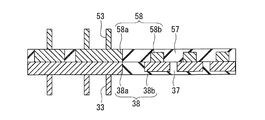
- FIG. 1 It is an enlarged cross-sectional view which shows the structure in the vicinity of the joint surface of the solid-state image pickup apparatus which concerns on 1st Embodiment of this disclosure.
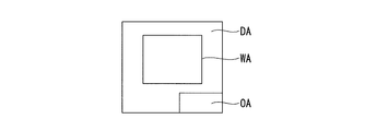
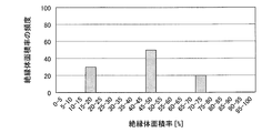
- FIG. 1 It is a plan schematic diagram which shows the wiring area WA, the dummy wiring area DA, and other area OA in the solid-state image sensor. Insulator of the fourth region A4 per unit area in the solid-state imaging device in which the ratio of the area of the fourth region A4 in the wiring region WA, the dummy wiring region DA and the other region OA is 48%, 73% and 18%, respectively. It is a graph which shows the frequency of the area ratio.
- FIG. 5 is an enlarged cross-sectional view showing a configuration in the vicinity of a joint surface of a solid-state image sensor when the joint position between the first substrate and the second substrate deviates from a predetermined position. It is a top view which shows the minimum structure of the 1st conductor and the 2nd conductor in the vicinity of the joint surface of the solid-state image pickup apparatus which concerns on 2nd Embodiment of this disclosure. It is an enlarged plan view which shows an example of the arrangement of the 1st conductor and the 2nd conductor in the vicinity of the joint surface of the solid-state image pickup apparatus which concerns on 2nd Embodiment of this disclosure.
- the present disclosure relates to a solid-state image sensor formed by joining a first substrate and a second substrate.
- the present disclosure also relates to a method for manufacturing a solid-state image sensor formed by joining a first substrate and a second substrate, and an electronic device having the solid-state image sensor. According to the present disclosure, when the first substrate and the second substrate are bonded, a decrease in bonding strength at the bonding surface between the first substrate and the second substrate is suppressed at any position on the bonding surface. be able to.
- voids (air bubbles) that cannot be partially bonded may be formed on the bonding surface between the first substrate and the second substrate.
- the joint surface in the case of a solid-state image sensor that does not have a region in which the insulating film exposed on the joint surface of the first substrate and the insulating film exposed on the joint surface of the second substrate are directly bonded, the joint surface. In, the joining strength immediately after joining becomes low. Then, when the bonding strength at the bonding surface between the substrates becomes low, voids (air bubbles) are likely to be formed on the bonding surface between the first substrate and the second substrate.
- the cause of voids is mainly the difference in joint strength.
- the bonding strength between copper and copper immediately after bonding the substrate and the bonding strength in the region where copper and the insulating film are directly bonded are lower than the bonding strength in the region where the insulating film and the insulating film are directly bonded. Therefore, in order to make it difficult for the first substrate and the second substrate to be separated from each other, the first insulating film provided on the first substrate and the second insulating film provided on the second substrate are formed. It is necessary to secure a certain ratio or more of the area to be directly joined even in the area of the joint surface throat.
- the present disclosure provides a technique for suppressing a decrease in bonding strength between substrates caused by bonding deviation between substrates so that the bonding strength becomes a certain level or higher at any position on the bonding surface.
- FIG. 1 is a block diagram showing a configuration example of the solid-state image sensor according to the present disclosure.
- the solid-state image sensor 1 is configured as, for example, a CMOS (Complementary Metal Oxide Semiconductor) image sensor.
- the solid-state image sensor 1 has a pixel region (pixel array) 3 in which a plurality of pixels 2 are regularly arranged in a two-dimensional array on a semiconductor substrate (for example, a Si substrate) (not shown), and a peripheral circuit unit.
- CMOS Complementary Metal Oxide Semiconductor
- Pixel 2 has a photoelectric conversion unit (for example, a photodiode) and a plurality of pixel transistors (MOS transistors).
- the plurality of pixel transistors can be composed of, for example, three transistors, a transfer transistor, a reset transistor, and an amplification transistor. Further, the plurality of pixel transistors may be composed of four transistors by adding a selection transistor. Since the equivalent circuit of a unit pixel is the same as the well-known technique, detailed description thereof will be omitted.
- the pixel 2 can be configured as one unit pixel or can have a shared pixel structure.
- This pixel sharing structure is a structure in which a plurality of photodiodes share a transistor other than the floating diffusion and the plurality of transfer transistors. That is, in the shared pixel, the photodiode and the transfer transistor constituting the plurality of unit pixels are configured by sharing the other pixel transistor.
- the peripheral circuit unit includes a vertical drive circuit 4, a column signal processing circuit 5, a horizontal drive circuit 6, an output circuit 7, and a control circuit 8.
- the vertical drive circuit 4 is composed of, for example, a shift register.
- the vertical drive circuit 4 selects the pixel drive wiring, supplies a pulse for driving the pixel to the selected pixel drive wiring, and drives the pixel in line units. That is, the vertical drive circuit 4 selectively scans each pixel 2 of the pixel array 3 in a row-by-row manner in the vertical direction. Then, the vertical drive circuit 4 supplies a pixel signal based on the signal charge generated according to the amount of received light in the photoelectric conversion unit of each pixel 2 through the vertical signal line L1 to the column signal processing circuit 5.
- the column signal processing circuit 5 is arranged for each row of pixels 2, for example.
- the column signal processing circuit 5 performs signal processing such as noise removal for each pixel string for the signal output from the pixel 2 for one row.
- the column signal processing circuit 5 performs signal processing such as CDS (Correlated Double Sampling) for removing fixed pattern noise peculiar to pixel 2, signal amplification, and A / D (Analog / Digital) conversion. ..
- a horizontal selection switch (not shown) is provided in the output stage of the column signal processing circuit 5 so as to be connected to the horizontal signal line L2.
- the horizontal drive circuit 6 is composed of, for example, a shift register.
- the horizontal drive circuit 6 sequentially outputs horizontal scanning pulses to sequentially select each of the column signal processing circuits 5, and outputs pixel signals from each of the column signal processing circuits 5 to the horizontal signal line L2.
- the output circuit 7 performs signal processing on the signals sequentially supplied from each of the column signal processing circuits 5 through the horizontal signal line L2 and outputs the signals.
- the output circuit 7 may, for example, perform only buffering, or may perform black level adjustment, column variation correction, various digital signal processing, and the like.
- the control circuit 8 receives an input clock and data for instructing an operation mode and the like, and outputs data such as internal information of the solid-state image sensor 1. Further, the control circuit 8 obtains a clock signal or a control signal that serves as a reference for the operation of the vertical drive circuit 4, the column signal processing circuit 5, the horizontal drive circuit 6, etc., based on the vertical synchronization signal, the horizontal synchronization signal, and the master clock. Generate. Then, the control circuit 8 inputs these signals to the vertical drive circuit 4, the column signal processing circuit 5, the horizontal drive circuit 6, and the like. The input / output terminal 9 exchanges signals with the outside.
- FIGS. 2 to 4 are schematic views showing an example of a laminated structure of the solid-state image sensor 1 according to the present disclosure.
- An example of a laminated structure of the solid-state image sensor 1 to which the present disclosure is applied will be described with reference to FIGS. 2 to 4.
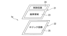
- the solid-state image sensor 1a shown in FIG. 2 is composed of a first substrate 11 and a second substrate 12.
- the pixel array 23 and the control circuit 24 are mounted on the first substrate 11.
- a logic circuit 25 including a signal processing circuit is mounted on the second substrate 12.
- the first substrate 11 and the second substrate 12 are electrically connected to each other to form a solid-state image sensor 1a as one substrate.
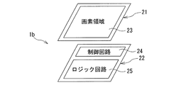
- the solid-state image sensor 1b shown in FIG. 3 is composed of a first substrate 11 and a second substrate 12.
- the pixel array 23 is mounted on the first substrate 11.
- a control circuit 24 and a logic circuit 25 including a signal processing circuit are mounted on the second substrate 12. Then, the first substrate 11 and the second substrate 12 are electrically connected to each other to form a solid-state image sensor 1b as one substrate.
- the solid-state image sensor 1c shown in FIG. 4 is composed of a first substrate 11 and a second substrate 12.
- a pixel array 23 and a control circuit 24-1 for controlling the pixel array 23 are mounted on the first substrate 11.
- a control circuit 24-2 for controlling the logic circuit 25 and a logic circuit 25 including a signal processing circuit are mounted on the second substrate 12. Then, the first substrate 11 and the second substrate 12 are electrically connected to each other to form a solid-state image sensor 1c as one substrate.
- CMOS image sensor two or more substrates may be bonded together.
- a substrate provided with a memory element array, a substrate provided with other circuit elements, and the like are added, and three or more substrates are bonded together to form one laminated substrate. It is also possible to configure a CMOS image sensor.
- FIG. 5 is a cross-sectional view showing a configuration example of the solid-state imaging device 1A according to the first embodiment of the present disclosure.
- the solid-state image sensor 1A is a back-illuminated CMOS (Complementary MOS) image sensor, and is an example of the solid-state image sensor 1.
- the back-illuminated CMOS image sensor is a CMOS image sensor in which the light receiving portion is arranged at the upper part of the circuit portion and has higher sensitivity and lower noise than the front-illuminated type.
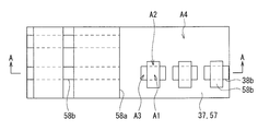
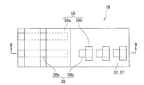
- FIG. 6 is an enlarged plan view showing a configuration in the vicinity of the joint surface of the solid-state image sensor 1A.
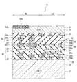
- FIG. 7 is a cross-sectional view taken along the line AA of FIG. 6, which is an enlarged cross-sectional view showing a configuration in the vicinity of the joint surface of the solid-state image sensor 1A.
- the solid-state image sensor 1A joins the first substrate 30 on which the plurality of first conductors 38 are formed and the first substrate 30 on which the plurality of second conductors 58 are formed.
- the second substrate 50 is provided.
- the first wiring 38a that is electrically conductive with the lower layer wiring 36 and the second wiring 58a that is electrically conductive with the multilayer wirings 55a and 55b and the upper layer wiring 56 are rectangular. It is formed in a shape.
- the first wiring 38a and the second wiring 58a are arranged so that at least a part of the first wiring 38a and the second wiring 58a overlap each other in a plan view.
- the first wiring 38a and the second wiring 58a having the same outer shape in the plan view are arranged so as to intersect each other in the plan view.
- Such a configuration is shown.
- the first wiring 38a and the second wiring 58a may be extended in the same direction and arranged so as to be displaced and overlap each other in a plan view.
- the first wiring 38a and the second wiring 58a may not have the same outer shape in a plan view and may have different sizes.
- the first wiring 38a is provided so as to extend in the left-right direction in FIG.
- the second wiring 58a is provided so as to extend in the vertical direction (an example of a direction intersecting with the first wiring 38a) in FIG.
- the first wiring 38a and the second wiring 58a are joined to each other at a portion where the first wiring 38a and the second wiring 58a overlap each other.
- the first conductor 38 and the second conductor 58 overlap each other on the joint surface 40 between the first substrate 30 and the second substrate 50. It has a first region A1.
- the solid-state image sensor 1A has a second region A2 on the joint surface 40 in which the first insulating film 37 and the second conductor 58 formed around the first conductor 38 overlap each other.
- the solid-state image sensor 1A has a third region A3 on the joint surface 40 in which the second insulating film 57 formed around the second conductor 58 and the first conductor 38 overlap each other.
- the solid-state image sensor 1A has a fourth region A4 in which the first insulating film 37 and the second insulating film 57 overlap each other on the joint surface 40.
- the first region A1 to the fourth region A4 are formed by arranging the first wiring 38a and the second wiring 58a so as to intersect each other in a plan view.
- the ratio of the area of the fourth region A4 per unit area (hereinafter, may be referred to as the insulator area ratio) is set to a predetermined value or more at any position of the joint surface 40. Be placed.
- the first wiring 38a (an example of the first conductor portion) that is electrically conductive with the lower layer wiring 36 and the lower layer It includes a wiring 36 and a first dummy wiring 38b (an example of a second conductor portion) having no electrical continuity.
- the first wiring 38a includes, for example, a connection pad for connecting the first substrate 30 and the second substrate 50, lateral wiring, an electromagnetic shield, and the like.
- the second conductor 58 As the second conductor 58, the second wiring 58a (an example of the third conductor portion) that electrically conducts with the multi-layer wiring 55a and 55b and the upper layer wiring 56, and the wiring 55a. , 55b and the upper layer wiring 56 and a second dummy wiring 58b (an example of a fourth conductor portion) having no electrical continuity.
- the second conductor 58 may include, for example, a connection pad for connecting the first substrate 30 and the second substrate 50, lateral wiring, an electromagnetic shield, and the like.
- the first conductor 38 and the second conductor 58 for performing Cu-Cu bonding are such that a part of the wiring is exposed on the bonding surface 40 which is the surface of the wiring layer of the first substrate 30 and the second substrate 50. Is formed in.
- the first conductor 38 and the second conductor 58 may or may not be electrically connected between the first substrate 30 and the second substrate 50 by Cu-Cu bonding.
- the connection pad for connecting the first substrate 30 and the second substrate 50 includes the pixels of the second substrate 50 (photodiode PD or pixel transistor serving as a photoelectric conversion unit) and signal processing of the first substrate 30. Connect with the circuit.
- the lateral wiring is a connection portion for supplying electric power supplied from the outside to each portion in the chip.
- the electromagnetic shield electrically shields between the first substrate 30 and the second substrate 50 with a Cu-Cu connection so that unintended electrical noise does not affect each wiring or transistor.
- first dummy wiring 38b and the second dummy wiring 58b do not function as a path for a pixel signal, and improve the joint strength between the first substrate 30 and the second substrate 50, dishing, and erosion. Is placed to suppress the. That is, the first dummy wiring 38b and the second dummy wiring 58b are electrically connected to the photodiode PD serving as the photoelectric conversion unit and the first wiring 38a and the second wiring 58a that are electrically connected to the photodiode PD. Is separated.
- the first dummy wiring 38b and the second dummy wiring 58b can be floated, but are electrically connected to a fixed potential such as a reference potential (GND) or a power supply voltage (VDD).
- the wiring area WA (an example of the first wiring area) of the solid-state image sensor 1A is provided with a first wiring 38a and a second wiring 58a including a connection pad, a lateral wiring, and an electromagnetic shield. Further, a first dummy wiring 38b and a second dummy wiring 58b are provided in the dummy wiring region DA (an example of the second wiring region) of the solid-state image sensor 1A.
- the first substrate 30 and the second substrate 50 are also formed with wiring that is not exposed on the joint surface 40.
- the first wiring 38a that is electrically conductive with the lower layer wiring 36, the multilayer wirings 55a and 55b, and the upper layer wiring 56 are electrically conductive.
- Wiring 58a of 2 is formed.
- a first dummy wiring 38b and a second dummy wiring 58b are formed in the dummy wiring region DA of the solid-state image sensor 1A.
- the dummy wiring area DA has been illustrated as an example of the “second wiring area”, but the present invention is not limited to this.
- the "second wiring region” it may be a region (another region OA) in which a conductor other than the first dummy wiring 38b and the second dummy wiring 58b is formed.
- the ratio of the area of the fourth region A4 (insulator area ratio) in which the first insulating film 37 and the second insulating film 57 overlap each other per unit area is the joint surface 40.
- the value is equal to or higher than the predetermined value at any of the positions.
- the bonding force between the first substrate 30 and the second substrate 50 can be maintained above a certain value.
- the ratio of the area of the fourth region A4 in which the first insulating film 37 and the second insulating film 57 overlap each other per unit area is a predetermined value at any position of the joint surface 40. It is as follows.
- the ratio of the area of the fourth region A4 per unit area is equal to or greater than a predetermined value having a predetermined bonding force between the first substrate 30 and the second substrate 50.
- the ratio of the area of the fourth region A4 per unit area is preferably 15% or more and 70% or less.
- the joint area between the first wiring 38a and the second wiring 58a becomes a certain ratio or more.
- the ratio of the area of the fourth region A4 per unit area is the surface condition of the first insulating film 37 and the second insulating film 57 to be joined, and the first insulating film 37 for each joining position.
- the preferable ratio changes depending on the ratio of the second insulating film 57. Therefore, the preferable value of the ratio of the area of the fourth region A4 per unit area varies over a wide numerical range.
- the "ratio of the area of the fourth region A4 per unit area” is the ratio of the area of the fourth region A4 per unit area on the joint surface 40.
- the joint surface 40 includes all of the wiring region WA and the dummy wiring region DA of the solid-state image sensor 1A, and all other regions OA except the wiring region WA and the dummy wiring region DA. Therefore, the solid-state image sensor 1A is designed so that the ratio of the area of the fourth region A4 per unit area is equal to or greater than a predetermined value in any of the wiring region WA, the dummy wiring region DA, and the other region OA. Will be done.
- the ratio of the area of the plurality of fourth regions A4 in the wiring area WA is different from the ratio of the area of the plurality of fourth regions A4 in the dummy wiring area DA. Further, it is preferable that the difference between the maximum value and the minimum value of the ratio of the area of the fourth region A4 per unit area (insulator area ratio) is equal to or less than a predetermined value at any position of the joint surface 40. .. Further, it is more preferable that the ratio of the area of the fourth region A4 per unit area in the dummy wiring region DA is larger than the ratio of the area of the fourth region A4 per unit area in the wiring region WA.
- the difference between the maximum value and the minimum value of the ratio of the area of the fourth region A4 (insulator area ratio) per unit area of 5 mm ⁇ 5 mm is preferably 10% or less, for example.
- the difference between the maximum value and the minimum value of the ratio of the area of the fourth region A4 per unit area is% or less, the first substrate 30 and the second substrate 50 are to some extent at any position of the joint surface 40. It is preferable because it joins uniformly and voids are less likely to occur on the joint surface 40.
- the "difference between the maximum value and the minimum value of the ratio of the area of the fourth region A4 per unit area" is defined as that of the plurality of fourth regions A4 in the plurality of predetermined regions of the joint surface 40 partitioned by the unit area.
- the difference between the maximum value and the minimum value of the area ratio is defined by the difference between the ratio of the area of the plurality of fourth regions A4 in the wiring region WA and the ratio of the area of the plurality of fourth regions A4 in the dummy wiring region DA.
- the above-mentioned “difference” may be a difference at any two locations of the connection pad of the wiring region WA, the lateral wiring, and the electromagnetic shield, or may be a difference at two locations in the dummy wiring region DA. good.
- the above-mentioned “maximum value” and “minimum value” are the maximum value and the maximum value among the values obtained by calculating the ratio of the area of the fourth region A4 from the coverage rate per unit area of the layout of the joint surface 40 of the solid-state image sensor 1. This is the minimum value.
- the "difference between the maximum value and the minimum value of the ratio of the area of the fourth region A4 per unit area" becomes large. .. That is, when the difference between the maximum value and the minimum value of the ratio of the area of the fourth region A4 per unit area is less than or equal to a predetermined value, the portion where the wiring density is locally increased on the entire surface of the layout is small. .. Therefore, joining the first substrate 30 and the second substrate 50 is preferable because the bonding properties of the bonding surface 40 become uniform and voids are less likely to occur on the bonding surface 40.
- FIG. 8 is a schematic plan view showing a wiring region WA, a dummy wiring region DA, and another region OA in a solid-state image sensor.
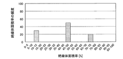
- FIGS. 9, 10 and 11 are graphs showing the frequency of the ratio of the area of the fourth region A4 per unit area (insulator area ratio) in the solid-state image sensor shown in FIG.
- the graph of FIG. 9 shows the ratio of the area of the fourth region A4 in the wiring region WA, the dummy wiring region DA, and the other region OA to 48%, 73%, and 18%, respectively, per unit area of the solid-state imaging device 1A.
- It is a graph which shows the frequency of the insulator area ratio of the 4th region A4.
- the graph of FIG. 10 shows the unit area in the solid-state imaging device 1A in which the ratios of the areas of the fourth region A4 in the wiring region WA, the dummy wiring region DA, and the other region OA are 48%, 76%, and 18%, respectively. It is a graph which shows the frequency of the insulator area ratio of the 4th region A4 per hit. That is, in the solid-state image sensor shown in FIG. 10, the ratio of the area of the fourth region in the dummy wiring region DA is slightly higher than that in the case shown in FIG. In such a solid-state image sensor, poor bonding occurs at the bonding surface between the first substrate and the second substrate.
- the graph of FIG. 11 shows the unit in the solid-state imaging device 1A in which the ratio of the area of the fourth region A4 in the wiring region WA, the dummy wiring region DA, and the other region OA is 48%, 73%, and 13%, respectively. It is a graph which shows the frequency of the insulator area ratio of the 4th region A4 per area. That is, in the solid-state image sensor shown in FIG. 11, the ratio of the area of the fourth region in the other region OA is slightly lower than that in the case shown in FIG. In such a solid-state image sensor, poor bonding occurs at the bonding surface between the first substrate and the second substrate.
- the ratio of the area of the fourth region A4 (insulator area ratio) to the bonding area of the first substrate 30 and the second substrate 50 is 15% or more and 70% or less.
- the first conductor 38 and the second conductor 58 in the vicinity of the joint surface 40 of the first substrate 30 and the second substrate 50 which is a characteristic configuration of the present embodiment, will be described in detail.
- the first wiring 38a and the second wiring 58a are arranged so that at least a part of the first wiring 38a and the second wiring 58a overlap each other in a plan view.
- the first wiring 38a and the second wiring 58a are arranged so as to intersect each other in a plan view.
- the first wiring 38a is provided so as to extend in the left-right direction in FIG.
- the second wiring 58a is provided so as to extend in the vertical direction (an example of a direction intersecting with the first wiring 38a) in FIG.
- first wiring 38a and the second wiring 58a are arranged so that the long side of the first wiring 38a and the long side of the second wiring 58a are orthogonal to each other in a plan view. As shown in FIG. 7, the first wiring 38a and the second wiring 58a are joined to each other at a portion where the first wiring 38a and the second wiring 58a overlap each other.
- the first dummy wiring 38b and the second dummy wiring 58b which have no electrical continuity with other portions, intersect each other in a plan view. It is arranged to do.
- the first dummy wiring 38b is provided so as to extend in the left-right direction in FIG.
- the second dummy wiring 58b is provided so as to extend in the vertical direction (an example of a direction intersecting with the first dummy wiring 38b) in FIG.
- the first dummy wiring 38b and the second dummy wiring 58b are arranged so that the long side of the first dummy wiring 38b and the long side of the second dummy wiring 58b are orthogonal to each other in a plan view. .. As shown in FIG. 7, the first dummy wiring 38b and the second dummy wiring 58b are joined to each other at a portion where the first dummy wiring 38b and the second dummy wiring 58b overlap each other.
- the first insulating film 37 of the first substrate 30 and the second substrate 50 are second.
- the ratio of the area where the insulating film 57 is directly bonded to the insulating film 57 can be made substantially constant at any position of the bonding surface 40.
- the ratio of the area where the first insulating film 37 and the second insulating film 57 are directly bonded is referred to as an "insulator area ratio”.
- a first substrate 30 on which a logic circuit 32 is formed, a pixel array, and a control circuit are formed. It has a laminated semiconductor substrate in which the second substrate 50 is bonded to the second substrate 50.
- the pixel array and the control circuit have the same configuration as the pixel array 23 and the control circuit 24 of the solid-state image sensor 1a shown in FIG.
- the first substrate 30 and the second substrate 50 are attached so that the surface on which the first conductor 38 is exposed and the surface on which the second conductor 58 is exposed face each other.
- the first substrate 30 and the second substrate 50 are directly joined by the first wiring 38a and the second wiring 58a, and the first dummy wiring 38b and the second dummy wiring 58b are directly joined. Arranged like this.
- the first substrate 30 has a configuration in which a logic circuit 32 constituting a peripheral circuit is formed on a first semiconductor substrate 31 made of silicon (Si).
- the logic circuit 32 is formed of a plurality of MOS transistors including CMOS transistors. As shown in FIG. 5, a plurality of regions on the surface side (upper side in FIG. 5) of the first semiconductor substrate 31 on which the logic circuit 32 is formed are interposed via a first insulating film 37 which is an interlayer insulating film.
- the wirings 35a to 35c of the layers (three layers in this embodiment) and the lower layer wiring 36 of one layer are formed.
- the wirings 35a to 35c are, for example, copper (Cu) wiring by the dual damascene method, and the lower layer wiring 36 is, for example, aluminum (Al) wiring.
- Each MOS transistor is formed and configured in the semiconductor well region on the surface side of the first semiconductor substrate 31.
- Each MOS transistor has a gate electrode formed via a gate insulating film with respect to a pair of source / drain regions and a pair of source / drain regions.
- Each MOS transistor is separated by, for example, an element separation region separated by an element separator having an STI structure.
- the multilayer wiring layer 34 is composed of the wirings 35a to 35c, the lower layer wiring 36, and the first conductor 38 composed of the first wiring 38a and the first dummy wiring 38b.
- the MOS transistor, the wiring 35a, and the wirings 35a to 35c of the adjacent upper and lower layers are connected to each other by the conductive first via 33.
- the first conductor 38 is made of metal.
- the first conductor 38 is provided so as to be exposed on a surface (joint surface 40) facing the second substrate 50.
- the first wiring 38a of the first conductor 38 is electrically connected to the lower layer wiring 36 and the wirings 35a, 35b, 35c via the first via 33, and is used as wiring.
- a pixel array in which a plurality of pixels are two-dimensionally arranged in a row is formed on a second semiconductor substrate 51 made of thinned silicon (Si).
- Each pixel is formed by a photodiode PD serving as a photoelectric conversion unit and a plurality of pixel transistors.
- a plurality of MOS transistors forming a control circuit are formed on the second semiconductor substrate 51.
- On the surface side (lower side in FIG. 5) of the second semiconductor substrate 51 a plurality of layers (three layers in this embodiment) wirings 55a and 55b and an upper layer are interposed via a second insulating film 57 which is an interlayer insulating film.
- Wiring 56 is formed.
- the wirings 55a and 55b and the upper layer wiring 56 are copper (Cu) wirings formed by, for example, the dual damascene method.
- a color filter 59a and an on-semiconductor chip are placed on the effective pixel array via an insulating film and a flattening film.
- a lens 59b is provided.
- an on-semiconductor chip lens 59b can be formed on an optical black region (not shown) formed via an insulating film of CIS 52.
- the multilayer wiring layer 54 is composed of the wirings 55a and 55b, the upper layer wiring 56, and the second conductor 58 composed of the second wiring 58a and the second dummy wiring 58b.
- the multilayer wiring layer 54 of the second substrate 50 between the corresponding pixel transistor and the wiring 55a, and between the adjacent upper and lower layer wirings 55a and 55b and the upper layer wiring 56 are connected by a conductive second via 53.
- the second conductor 58 is made of metal.
- the second conductor 58 is provided so as to be exposed on a surface (joint surface 40) facing the first substrate 30.
- the second wiring 58a of the second conductor 58 is electrically connected to the lower layer wiring 36 and the wirings 55a and 55b via the second via 53 and is used as wiring.
- the first substrate 30 and the second substrate 50 are arranged so that the multilayer wiring layers (multilayer wiring layers 34 and 54) of each other face each other, and the first wiring 38a and the second wiring are arranged on the joint surface 40.
- By directly joining the 58a they are electrically connected.
- a first insulating film 37 is formed in the vicinity of the joint surface 40 of the first substrate 30.
- a second insulating film 57 is formed in the vicinity of the joint surface 40 of the second substrate 50.
- the direct joining of the first wiring 38a and the second wiring 58a is performed by, for example, thermal diffusion joining.
- the first insulating film 37 and the second insulating film 57 other than the first wiring 38a and the second wiring 58a are joined by plasma joining or using an adhesive.
- an extremely thin and uniform insulating thin film is formed on the surfaces of the multilayer wiring layers (multilayer wiring layers 34 and 54) of each other.
- a film (not shown) may be formed and the first substrate 30 and the second substrate 50 may be bonded by plasma bonding or the like.
- a manufacturing method of the solid-state image sensor 1A will be shown with reference to FIG. First, a method of manufacturing the second substrate 50 will be described.
- a semiconductor well region is formed in a predetermined region of a second semiconductor wafer (hereinafter, referred to as a second semiconductor substrate 51) formed of silicon (Si).
- a photodiode PD that serves as a photoelectric conversion unit for each pixel is formed in this semiconductor well region.
- the device separation region can be formed first.
- Each photodiode PD is formed so as to extend in the depth direction of the semiconductor well region.
- the photodiode PD is formed in an effective pixel array that constitutes the pixel array 23 (see FIG. 2).
- a plurality of pixel transistors constituting each pixel are formed on the surface side of the semiconductor well region of the second semiconductor substrate 51.
- the pixel transistor can be composed of, for example, a transfer transistor, a reset transistor, an amplification transistor, and a selection transistor.
- Each pixel transistor is formed with a pair of source / drain regions and a gate electrode formed via a gate insulating film.
- An interlayer insulating film is formed on the upper surface side of the second semiconductor substrate 51, and a plurality of layers (three layers in this embodiment) wirings 55a and 55b and an upper layer wiring 56 and a second layer wiring 56 are formed of metal through the interlayer insulating film. And the via 53 of the above.
- the wirings 55a and 55b and the upper layer wiring 56 can be formed by the dual damascene method. That is, after forming a connection hole and a wiring groove by via first in the interlayer insulating film at the same time to form a Cu diffusion barrier metal film and a Cu seed film for preventing Cu diffusion, a Cu material layer is formed by a plating method. Embed.
- the Cu diffusion barrier metal film examples include tantalum (Ta), tantalum nitride (TaN), titanium (Ti), titanium nitride (TiN), tungsten (W), tungsten nitride (WN), ruthenium (Ru), and titanium nitride. Examples thereof include zirconium (TiZrN) and alloy films containing these.
- CMP chemical mechanical polishing
- an insulating film such as silicon nitride (SiN), silicon carbide (SiC), silicon carbide (SiCN), or silicon oxide (SiON) can be used. This step is repeated to form the three-layer wirings 55a and 55b and the upper layer wiring 56.
- a Cu diffusion barrier insulating film is formed on the interlayer insulating film on which the wirings 55a and 55b and the upper layer wiring 56 are formed, and then an insulating film having no Cu diffusion barrier property is formed.
- the Cu diffusion barrier insulating film the above-mentioned insulating film such as silicon nitride (SiN), silicon carbide (SiC), silicon carbide (SiCN), and silicon oxide (SiON) can be used.
- the insulating film having no Cu diffusion barrier property is formed of, for example, a silicon oxide (SiO 2 ) film, a SiCOH film, or the like.
- the insulating film having no Cu diffusion barrier property and the Cu diffusion barrier metal film on the outermost surface are patterned by via-first using lithography and etching techniques to selectively form openings that are via holes.
- an opening of the portion corresponding to the second wiring 58a and a via hole of the portion corresponding to the second via 53 are formed.
- a second via 53 and a second conductor 58 (second) that are electrically connected to the upper layer wiring 56 by embedding a Cu material in the opening and the via hole using the dual damascene method.
- the wiring 58a and the second dummy wiring 58b) are formed.
- the second wiring 58a is formed as a fourth metal layer.
- the second substrate 50 on which the wirings 55a and 55b formed of metal, the upper layer wiring 56, and the second conductor 58, and the multilayer wiring layer 54 including the second insulating film 57 are formed is formed.
- a semiconductor well region is formed in a predetermined region of a first semiconductor wafer (hereinafter referred to as a first semiconductor substrate 31) formed of silicon (Si).
- a plurality of MOS transistors forming the logic circuit 32 are formed in the semiconductor well region.
- the MOS transistor can be formed in the device separation region after forming, for example, an element separator having an STI structure.
- An interlayer insulating film is formed on the upper surface side of the first semiconductor substrate 31, and the wirings 35a, 35b and 35c of a plurality of layers (three layers in this embodiment) and the lower layer wiring 36 are formed of metal through the interlayer insulating film. , Forming the first via 33.
- the wirings 35a, 35b and 35c can be formed by the dual damascene method. That is, after forming a connection hole and a wiring groove by via first in the interlayer insulating film at the same time to form a Cu diffusion barrier metal film and a Cu seed film for preventing Cu diffusion, a Cu material layer is formed by a plating method. Embed.
- the Cu diffusion barrier metal film examples include tantalum (Ta), tantalum nitride (TaN), titanium (Ti), titanium nitride (TiN), tungsten (W), tungsten nitride (WN), ruthenium (Ru), and titanium nitride. Examples thereof include zirconium (TiZrN) and alloy films containing these.
- CMP chemical mechanical polishing
- the Cu barrier insulating film for example, an insulating film such as silicon nitride (SiN), silicon carbide (SiC), silicon carbide (SiCN), or silicon oxide (SiON) can be used. This step is repeated to form wirings 35a to 35c formed of three layers of metal. Further, the lower layer wiring 36 is formed by simultaneously forming a connection hole by via first and a wiring groove in the interlayer insulating film and embedding an Al material layer.
- a Cu diffusion barrier insulating film is formed on the interlayer insulating film in which the wirings 35a to 35c and the lower layer wiring 36 are formed, and then an insulating film having no Cu diffusion barrier property is formed.
- the Cu diffusion barrier insulating film the above-mentioned insulating film such as silicon nitride (SiN), silicon carbide (SiC), silicon carbide (SiCN), and silicon oxide (SiON) can be used.
- the insulating film having no Cu diffusion barrier property is formed of, for example, a silicon oxide (SiO 2 ) film, a SiCOH film, or the like.
- the insulating film having no Cu diffusion barrier property and the Cu diffusion barrier metal film on the outermost surface are patterned by via-first using lithography and etching techniques to selectively form openings that are via holes.
- an opening of the portion corresponding to the first wiring 38a and a via hole of the portion corresponding to the first via 33 are formed.
- a first via 33 and a first conductor 38 (first) that are electrically connected to the lower layer wiring 36 by embedding a Cu material in the opening and the via hole using the dual damascene method.
- the wiring 38a and the first dummy wiring 38b) are formed.
- the second wiring 58a is formed as a fifth metal layer.
- the first substrate 30 on which the wirings 35a to 35c formed of metal, the lower layer wiring 36 and the first conductor 38, and the multilayer wiring layer 34 including the first insulating film 37 are formed is formed. ..
- the first substrate 30 and the second substrate 50 are arranged and joined so that the multilayer wiring layers 34 and 54 face each other.
- the fourth region A4 per unit area has a predetermined bonding force between the first substrate 30 and the second substrate 50 at any position of the wiring region WA and the dummy wiring region DA.
- the first substrate 30 and the second substrate 50 are arranged so that the area ratio is equal to or greater than a predetermined value.
- the first conductor 38 exposed from the first substrate 30 and the second conductor 58 exposed from the second substrate 50 are joined. More specifically, the first wiring 38a and the second wiring 58a, the first dummy wiring 38b and the second dummy wiring 58b are joined, respectively.
- the first wiring 38a and the second wiring 58a arranged so as to intersect each other in a plan view are directly joined at a portion overlapping each other.
- the first dummy wiring 38b and the second dummy wiring 58b arranged so as to intersect each other in a plan view are directly joined at a portion overlapping each other.
- the first conductor 38 and the second conductor 58 are thermally diffused and joined by heat treatment.
- the heat treatment temperature at this time can be about 100 ° C. or higher and 500 ° C. or lower.
- the first insulating film 37 and the second insulating film 57 which are interlayer insulating films, are surface-treated and plasma-bonded.
- the first insulating film 37 and the second insulating film 57 can also be joined with an adhesive.
- the second semiconductor substrate 51 is ground and polished to a thin film by using a CMP method or the like so that the required film thickness of the photodiode PD remains from the back surface side.
- a color filter 59a and an on-semiconductor chip lens 59b are formed on the photodiode PD corresponding to the effective pixel array via the flattening film.
- a light-shielding film may be formed on the photodiode PD corresponding to the optical black region via an insulating film.
- the bonded first substrate 30 and the second substrate 50 are cut into semiconductor chips that are separated into semiconductor chips to obtain the solid-state image sensor 1A shown in FIG.
- the first wiring 38a and the second wiring 58a, the first dummy wiring 38b and the second dummy wiring 58b, the wirings 35a to 35c, the wirings 55a and 55b, and the lower layer wiring 36 and the upper layer wiring 56 are conductive. It is desirable that the material is made of a material having a high light-shielding property and easy to join. As a material having such properties, in addition to Cu, a single material such as aluminum (Al), tungsten (W), titanium (Ti), tantalum (Ta), molybdenum (Mo), ruthenium (Ru), or a single material, or Alloys can be used. Further, the film thicknesses of the first wiring 38a and the second wiring 58a and the first dummy wiring 38b and the second dummy wiring 58b are determined according to the wavelength of the light on the light emitting first substrate 30 side. desirable.
- a photodiode PD, a transistor, a multilayer wiring layer, or the like is formed on a semiconductor wafer, the semiconductor wafers are joined to each other, and then cut to form a semiconductor chip, that is, a so-called wafer-wafer.
- the solid-state imaging device 1A is formed by joining has been described, but the present invention is not limited to this.
- one of the first substrate 30 and the second substrate 50 is set as a chip substrate in which a semiconductor chip is formed in advance, and a wafer-chip junction in which a semiconductor chip (chip substrate) is bonded onto a semiconductor wafer.
- the solid-state image sensor 1A may be formed by the above.
- both the first substrate 30 and the second substrate 50 are made into semiconductor chips in advance, and the solid-state image sensor 1A is formed by chip-chip bonding in which semiconductor chips (chip substrates) are bonded to each other. It may be formed.
- the first substrate 30 or the second substrate 50 is a chip substrate as in wafer-chip bonding and chip-chip bonding, it is compared with the wafer-wafer bonding described in this embodiment.
- the method of holding the chip substrate at the time of joining, the method of pressing the chip substrate with a pin, the thickness of the chip substrate, and the like are changed during wafer-chip bonding and chip-chip bonding, the bonding speed at the time of chip substrate bonding and the direction vector in which the bonding proceeds change, so that the chip substrates behave differently from wafer-to-wafer bonding.
- the bonding speed and direction vector are uniform in the radial direction.
- the chip substrate is rectangular, there are differences in the bonding speed and direction vector from the center of the chip substrate.
- the influence of the width of the oxide film region at the edge of the substrate and the corner at the edge of the chip, which are related to the entrainment of the junction vector cannot be ignored.
- variations in bonding force can be suppressed even in the case of wafer-chip bonding and chip-chip bonding.
- the ratio of the area of the fourth region to the unit area in the solid-state image sensor 1A is the above-mentioned bonding speed and direction vector.
- the difference may be considered as an offset for determination.
- the sign of the offset can be positive for factors that promote bonding and negative for factors that inhibit bonding, for example.
- the sign of the offset is negative for the factor that promotes joining, and the factor that hinders it is positive. Can be.
- the method of pressing the pins and the device of the bonding device at the time of substrate bonding are devised. Take measures such as going and devising the layout.
- the conductor has been described as a dummy, but the use of the conductor is not limited to the dummy, and the conductor can be used for purposes such as dummy wiring and alignment marks.
- the solid-state image sensor 1A has the following effects.
- the conductor 38 and the second conductor 58 are joined. That is, in the solid-state imaging device 1A, the first wiring 38a and the second wiring 58a intersect in a plan view, and the first dummy wiring 38b and the second dummy wiring 58b intersect in a plan view.
- the first substrate 30 and the second substrate 50 are arranged.
- the joint area between the first conductor 38 and the second conductor 58 (the area of the first region A1) becomes substantially constant even when one of the substrates is slightly displaced from the predetermined position. ..
- the area of the fourth region A4 where the first insulating film 37 and the second insulating film 57 overlap is also substantially constant. Therefore, the solid-state image sensor 1A has the bonding strength of the first substrate 30 and the second substrate 50 even when the position shift occurs when the first substrate 30 and the second substrate 50 are bonded.
- the stability is high, and voids are less likely to occur on the joint surface 40.
- the ratio of the area of the fourth region A4 per unit area (insulator area ratio) on the joint surface 40 is preferably 15% or more and 70% or less in any region.
- Solid-state image sensor according to the second embodiment
- the solid-state image sensor (image sensor) according to the second embodiment of the present disclosure will be described with reference to FIGS. 15 to 18.
- the first conductor 38 and the second conductor 58 intersect each other in a plan view, and the first insulating film 37 and the second insulating film 57 overlap each other on the joint surface 40.
- the solid-state image sensor 1A in which the ratio of the areas of the four regions A4 is equal to or larger than a predetermined value has been described.
- the solid-state image sensor 1B which is a modification of the solid-state image sensor 1A, will be described.
- the solid-state image sensor 1B differs from the solid-state image sensor 1A in that the first conductor 138 and the second conductor 158 are provided in place of the first conductor 38 and the second conductor 58.
- FIGS. 15 and 16 show a configuration in the vicinity of the joint surface of the solid-state image sensor 1A when the joint position between the first substrate 30 and the second substrate 50 deviates from a predetermined position.
- FIG. 15 is an enlarged plan view showing a configuration in the vicinity of the joint surface of the solid-state image sensor 1A when the joint position between the first substrate 30 and the second substrate 50 deviates from a predetermined position.
- FIG. 16 is a cross section taken along the line BB of FIG. 15, and shows a configuration in the vicinity of the joint surface of the solid-state image sensor 1B when the joint position between the first substrate 30 and the second substrate 50 deviates from a predetermined position. It is an enlarged sectional view.
- the causes of this deviation include a deviation due to a process such as a dimensional deviation of the mask, an alignment deviation of the exposure apparatus, and an alignment deviation of the joining apparatus, and a deviation when the pattern is shifted for the purpose of shading.
- a deviation of less than or equal to the maximum deviation amount ⁇ expected in advance occurs when the first substrate 130 and the second substrate 150 are bonded, a decrease in bonding strength is suppressed and a void is formed. Can be suppressed.
- FIG. 17 is a plan view showing the minimum configuration of the first conductor 138 and the second conductor 158 in the vicinity of the joint surface of the solid-state image sensor 1B.
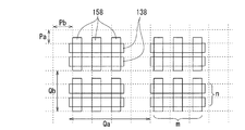
- FIG. 18 is an enlarged plan view showing an example of the configuration of the first conductor 138 and the second conductor 158 in the vicinity of the joint surface of the solid-state image sensor 1B.
- the first conductor 138 is either the first wiring 138a or the first dummy wiring 138b.
- the second conductor 158 is the second wiring 158a when the first conductor 138 is the first wiring 138a, and the first conductor 138 is the first dummy wiring 138b. , The second dummy wiring 158b.
- the cross-sectional configuration of the portion of the solid-state image sensor 1B other than the configuration near the joint surface is the same as the configuration of the solid-state image sensor 1A shown in FIG.
- the first conductor 138 and the second conductor 158 are arranged so as to intersect each other in a plan view.
- the first conductor 138 is provided so as to extend in the left-right direction in FIG.
- the second conductor 158 is provided so as to extend in the vertical direction (an example of a direction intersecting with the first conductor 138) in FIG.
- the first conductor 138 and the second conductor 158 are arranged so as to intersect with each other in the dummy wiring region DA.
- the first conductor 138 is provided so as to extend in the left-right direction in FIG.
- the second conductor 158 is provided so as to extend in the vertical direction (an example of a direction intersecting with the first conductor 138) in FIG.
- the first conductor 138 (first conductor 138) in the vicinity of the joint surface of the solid-state imaging device 1B has a long side length (length in the stretching direction of the pattern) La and a short side. (Length in the direction orthogonal to the stretching direction) Wa is formed in a rectangular shape.
- the second conductor 158 (second conductor 158) in the vicinity of the joint surface of the solid-state imaging device 1B has a long side length (length in the stretching direction of the pattern) Lb and a short side length (stretching). It is formed in a rectangular shape of Wb (length in the direction orthogonal to the direction).
- a plurality of (n) first conductors 138 provided parallel to each other and a plurality (m) second conductors provided parallel to each other are provided. It has a plurality of wiring groups having a body 158.
- the two first conductors 138 provided parallel to each other are arranged at a pitch Pa in the pattern width direction (vertical direction in FIG. 18).
- the three second conductors 158 provided parallel to each other are arranged at a pitch Pb in the pattern width direction (left-right direction in FIG. 18).
- the wiring group composed of the two first conductors 138 and the three second conductors 158 has a pattern extending direction of the first conductor 138 with respect to the adjacent wiring groups (left and right in FIG. 18). They are arranged at a pitch Qa in the direction) and a pitch Qb in the pattern width direction (vertical direction in FIG. 18) of the first conductor 138.
- the ratio of the area of the fourth region A4 is constant even when a deviation of less than or equal to the maximum deviation amount ⁇ assumed in advance occurs when the first substrate 130 and the second substrate 150 are joined.
- the sizes of the first conductor 138 and the second conductor 158 are adjusted so as to be. That is, the first conductor 138 and the second conductor 158 are formed so that the insulator area ratio is constant at a preset value.
- the amount of deviation ⁇ depends on the position accuracy of the joining device that joins the first substrate 130 and the second substrate 150. Therefore, the dimensions of the first conductor 138 and the second conductor 158 are designed according to the positional accuracy of the joining device.
- Insulator area ratio (Dss) in the dummy wiring region DA is represented by the following equation (1).
- Insulator area ratio (Dss) ⁇ Qa ⁇ Qb- (La ⁇ Wa ⁇ n + Lb ⁇ Wb ⁇ m-Wa ⁇ Wb ⁇ n ⁇ m) ⁇ / (Qa ⁇ Qb) ⁇ ⁇ ⁇ (1)
- the pattern width W of the first dummy wiring 138b and the second dummy wiring 158b is determined so as to satisfy the following equation (3) from the step constraint.
- the length La of the first conductor 138 and the pattern width Wb of the second conductor 158 are determined to satisfy the following equation (4) due to the alignment deviation constraint based on the maximum deviation amount ⁇ of the alignment deviation. .. That is, the difference between the length of the long side of the first conductor 138 and the length of the short side of the second conductor 158 is more than twice the maximum deviation amount ⁇ assumed in advance.
- the shapes of the first conductor 138 and the second conductor 158 satisfying the above formulas (1) to (6) will be specifically described.
- the pattern width W satisfying the equation (4) is given by W ⁇ 1.8 ⁇ m. Further, the pattern width W satisfying the equation (5) is given by W ⁇ 2.8 ⁇ m. Further, due to the restrictions of the equations (3) and (6), 0.5 ⁇ W ⁇ 2.3 is a preferable range in the solid-state image sensor 1B.
- the pattern width W of the first conductor 138 and the second conductor 158 is preferably in the range of W ⁇ 1.8 ⁇ m from the results of both.
- the pattern width Wa and length La of the first conductor 138 and the pattern width Wb and length Lb of the second conductor 158 described in the present embodiment are the above-mentioned insulator area ratio (Dss) and the above-mentioned insulator area ratio (Dss). If the deviation constraint is satisfied, it can be set freely.
- the pitch Pa between the first conductors 138, the pitch Pb between the second conductors 158, and the pitches Qa and Qb between the wiring groups also deviate from the above-mentioned insulator area ratio (Dss). If the restrictions are met, it can be set freely.
- the dimensions of the first conductor 138 and the second conductor 158 are designed based on the constraints described above.
- the bonding area between the first insulating film 137 and the second insulating film 157 (insulator) even if the bonding is misaligned at the time of bonding. Area ratio) can be constant.
- the stability of the bonding strength between the first substrate 130 and the second substrate 150 (neither shown) on the bonding surface 140 is increased, and voids are generated by preventing bonding defects on the bonding surface 140. It becomes difficult.
- the solid-state image sensor 1B according to the present embodiment has the following effects in addition to the effect of the first embodiment.
- the shapes of the first insulating film 137 and the second insulating film 157 are designed according to the maximum amount ⁇ of the misalignment between the first substrate 130 and the second substrate 150. Can be done.
- the bonding area (insulator area ratio) between the first insulating film 137 and the second insulating film 157 can be kept constant even if the bonding is misaligned at the time of bonding. Therefore, the stability of the bonding strength between the first substrate 130 and the second substrate 150 (neither shown) on the bonding surface 140 becomes high, and voids are generated by preventing the bonding failure on the bonding surface 140. It becomes difficult.
- Solid-State Image Sensor of Third Embodiment the solid-state image sensor (image sensor) according to the third embodiment of the present disclosure will be described with reference to FIGS. 19 to 27.
- the first conductor 38 and the second conductor 58 intersect each other in a plan view, and the first insulating film 27 and the second insulating film 57 per unit area on the joint surface 40.
- the solid-state image sensor 1A in which the ratio of the area of the fourth region A4 that overlaps with the above is equal to or more than a predetermined value has been described.
- the shapes of the first conductor 38 and the second conductor 58 are defined in more detail with respect to the deviation between the first substrate 30 and the second substrate 50.
- the solid-state image sensors 1C to 1F will be described.
- FIG. 19 is an enlarged plan view showing a configuration in the vicinity of the joint surface of the solid-state image sensor 1C, which is the first example.
- the two first wirings 238a and the two second wirings 258a are arranged so as to intersect each other in the plan view in the wiring region WA.
- the first wiring 238a is provided so as to extend in the left-right direction in FIG.
- the second wiring 258a is provided so as to extend in the vertical direction (an example of a direction intersecting with the first wiring 238a) in FIG.
- a plurality of first dummy wirings 238b and second dummy wirings 258b are arranged so as to intersect each other in the dummy wiring region DA.
- the first dummy wiring 238b is provided so as to extend in the left-right direction in FIG.
- the second dummy wiring 258b is provided so as to extend in the vertical direction (an example of a direction intersecting with the first dummy wiring 238b) in FIG.
- the first dummy wiring 238b and the second dummy wiring 258b are formed, for example, in the same size.
- the shape (planar shape) exposed on the joint surface 240 of the first dummy wiring 238b and the second dummy wiring 258b is a rectangular shape having a length L in the extending direction of the pattern and a pattern width W.
- the first dummy wiring 238b is arranged at a pitch P with respect to the adjacent first dummy wiring 238b.
- the second dummy wiring 258b is also arranged at a pitch P with respect to the adjacent second dummy wiring 258b.
- the first dummy wiring 238b and second dummy wiring 258b it is arranged to overlap in the area W 2. It is preferable that the second dummy wiring 258b is overlapped at a position inside the distance of the maximum deviation amount ⁇ or more from both ends of the first dummy wiring 238b in the left-right direction.
- the insulator area ratio (Dss) is determined so as to satisfy the following equation (12) from the overlap constraint of the first insulating film 237 and the second insulating film 257.
- the pattern width W of the first dummy wiring 238b and the second dummy wiring 258b is determined so as to satisfy the following equation (13) from the step constraint.
- the pattern width W satisfying the equation (14) is given by W ⁇ 8.8 ⁇ m.
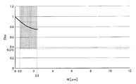
- FIG. 20 shows equations (11) to (14) in the solid-state image sensor 1C.
- the range of W that satisfies the constraints of the equations (11) and (12) is W ⁇ 4.7 from the intersection of the equations (11) and (12). This value satisfies the constraint of equation (14).
- 0.5 ⁇ W ⁇ 4.7 is a preferable range in the solid-state image sensor 1C.
- the pattern width W satisfying the equation (14) is given by W ⁇ 2.3 ⁇ m.
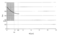
- FIG. 21 shows equations (11) to (15) in the solid-state image sensor 1D. As shown in FIG. 21, the range of W that satisfies the constraints of the equations (11) and (12) is W ⁇ 2.3 because there is no intersection of the equations (11) and (12). Further, due to the restrictions of the equations (13) and (15), 0.5 ⁇ W ⁇ 2.3 is a preferable range in the solid-state image sensor 1D.
- FIG. 22 is an enlarged plan view showing a configuration in the vicinity of the joint surface of the solid-state image sensor 1E, which is the third example.
- the two first wirings 238a and the two second wirings 258a are arranged so as to intersect each other in the plan view in the wiring region WA.
- the first wiring 238a is provided so as to extend in the left-right direction in FIG. 22.
- the second wiring 258a is provided so as to extend in the vertical direction (an example of a direction intersecting with the first wiring 238a) in FIG. 22.
- one first dummy wiring 238b and three second dummy wirings 258b are arranged intersecting each other in the dummy wiring area DA.
- the first dummy wiring 238b is provided so as to extend in the left-right direction in FIG. 22.
- the second dummy wiring 258b is provided so as to extend in the vertical direction (an example of a direction intersecting with the first dummy wiring 238b) in FIG. 22.
- a plurality of wiring groups (four in the present embodiment) in which one first dummy wiring 238b and three second dummy wirings 258b are arranged intersecting with each other are formed.
- FIG. 23 shows equations (1) to (6) in the solid-state image sensor 1E.
- the range of W that satisfies the constraints of the equations (1) and (2) is W ⁇ 1.8 because there is no intersection of the equations (1) and (2).
- 0.5 ⁇ W ⁇ 1.8 is a preferable range in the solid-state image sensor 1D.
- FIG. 24 is an enlarged plan view showing a configuration in the vicinity of the joint surface of the solid-state image sensor 1F, which is the third example.
- the two first wirings 238a and the two second wirings 258a are arranged so as to intersect each other in a plan view in the wiring region WA.
- the first wiring 238a is provided so as to extend in the left-right direction in FIG. 24.
- the second wiring 258a is provided so as to extend in the vertical direction (an example of a direction intersecting with the first wiring 238a) in FIG. 24.
- first dummy wirings 238b and one second dummy wiring 258b are arranged so as to intersect each other in the dummy wiring area DA.
- the first dummy wiring 238b is provided so as to extend in the left-right direction in FIG. 24.
- the second dummy wiring 258b is provided so as to extend in the vertical direction (an example of a direction intersecting with the first dummy wiring 238b) in FIG. 24.
- a plurality of wiring groups (nine in the present embodiment) in which two first dummy wirings 238b and one second dummy wiring 258b are arranged intersecting with each other are formed.
- the pattern width W satisfying the formula (4) is given by W ⁇ 2.3 ⁇ m
- the pattern width W satisfying the formula (5) is given by W ⁇ 1.8 ⁇ m.
- the pattern width W satisfying the equation (1) is given by W ⁇ 1.6 ⁇ m.
- FIG. 25 shows equations (1) to (6) in the solid-state image sensor 1F. As shown in FIG. 25, the range of W that satisfies the constraints of the equations (1) and (2) is W ⁇ 1.6. Further, due to the restrictions of the equations (3) and (6), 0.5 ⁇ W ⁇ 1.6 is a preferable range in the solid-state image sensor 1F.
- the first dummy wiring 238b and bonding area between the second dummy wiring 258b remains at W 2.
- the bonding area between the first dummy wiring 238b and second dummy wiring 258b is changed from W 2 May be done.
- the joint area between the first dummy wiring 238b and the second dummy wiring 258b becomes constant (W 2 )
- the joint area between the first dummy wiring 238b and the second insulating film 257, the second The joint area between the dummy wiring 258b and the first insulating film 237 is also constant. Therefore, the bonding area (insulator area ratio) between the first insulating film 237 and the second insulating film 257 is also constant. From the above, the stability of the bonding strength between the first substrate 230 and the second substrate 250 on the bonding surface 240 becomes high, and voids are less likely to occur on the bonding surface 240.
- FIGS. 26 and 27 show other configuration examples of the solid-state image sensors 1C to 1F.
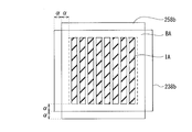
- the outer peripheral region of the first region A1 where the first dummy wiring 238b and the second dummy wiring 258b overlap in a plan view is the first dummy wiring 238b and the first dummy wiring 238b. It may be secured as the joint region BA with the dummy wiring 258b of 2.
- the joining region BA is preferably a region at least inside the alignment deviation amount ⁇ from the outer circumference of the first region A1, for example. Further, in the solid-state image pickup devices 1C to 1F shown in FIG.
- the first insulating film 237 and the second insulating film 257 are provided in a region other than the bonding region BA between the first dummy wiring 238b and the second dummy wiring 258b. It may be arranged.
- the junction region BA is a region outside the region surrounded by the broken line in FIG. 26, and the arrangement region of the first insulating film 237 and the second insulating film 257 (hereinafter referred to as the insulating film arrangement region) IA is , The area surrounded by the broken line in FIG. 26.
- the shape of the insulating film arrangement region IA surrounded by the broken line in FIG. 26 is rectangular, but the shape is not limited to this.
- the insulating film arrangement region IA may have any shape such as a circle or a polygon.
- a plurality of insulating films may be arranged in the insulating film arrangement region IA.
- the solid-state image sensors 1C to 1F shown in FIG. 27 show an example in which a plurality of rectangular insulating films are arranged in a stripe shape in the insulating film arrangement region IA.
- the solid-state image sensors 1C to 1F according to the present embodiment have the following effects in addition to the effects of the first embodiment.
- the shapes of the first conductor 238 and the second conductor 258 (the first) according to the maximum amount ⁇ of the misalignment between the first substrate 230 and the second substrate 250.
- the dimensions of the first wiring 238a and the second wiring 258a, and the first dummy wiring 238b and the second dummy wiring 258b) can be designed.
- the insulator area ratio (Dss) becomes constant at a preset value, and the stability of the bonding strength between the first substrate 230 and the second substrate 250 on the bonding surface 240 becomes high. Voids are less likely to occur.
- Solid-state image sensor according to the fourth embodiment
- the solid-state image sensor (image sensor) according to the fourth embodiment of the present disclosure will be described with reference to FIGS. 28 to 30.
- the first conductor 38 and the second conductor 58 intersect each other in a plan view, and the first insulating film 37 and the second insulating film 57 per unit area on the joint surface 40.
- the solid-state image sensor 1G having a configuration in which the first conductor 38, the second conductor 58, the first insulating film 37, and the second insulating film 57 are inverted will be described. do. That is, in the solid-state image sensor 1G, the rectangular first insulating film 337 and the second insulating film 357 are arranged so that at least a part of them overlap each other and intersect with each other in a plan view. In the solid-state image sensor 1G, a first conductor 338 and a second conductor 358 are provided around the first insulating film 337 and the second insulating film 357.
- FIG. 28 is an enlarged plan view showing a configuration in the vicinity of the joint surface of the solid-state image sensor 1G.
- FIG. 29 is a CC cross section of FIG. 28, which is an enlarged cross section showing a configuration in the vicinity of the joint surface of the solid-state image sensor 1G.
- the overall configuration of the solid-state image sensor 1G that is, the cross-sectional configuration of the portion other than the configuration near the joint surface of the solid-state image sensor 1G is the same as the configuration of the solid-state image sensor 1A shown in FIG.
- the solid-state image sensor 1G is joined to the first substrate 330 on which the first conductor 338 is formed and the first substrate 330 on which the second conductor 358 is formed.
- a second substrate 350 is provided.
- the first via 33 is connected to the first conductor 338
- the second via 35 is connected to the second conductor 358.
- the display of the first via 33 and the second via 35 shown in FIG. 8 is omitted.
- the solid-state image sensor 1G includes a rectangular first insulating film portion 337a and a second insulating film portion 357a, and a rectangular first dummy insulating film portion 337b and a second dummy insulating film portion 357b. doing.
- the first insulating film portion 337a and the second insulating film portion 357a are provided at positions corresponding to the first wiring 38a and the second wiring 58a of the solid-state image sensor 1A according to the first embodiment, respectively. ing.
- the solid-state image sensor 1G includes a first insulating film portion 337a and a first dummy insulating film portion 337b as the first insulating film 337. Further, the solid-state image sensor 1G includes a second insulating film portion 357a and a second dummy insulating film portion 357b as the second insulating film 357.
- the rectangular first dummy insulating film portion 337b and the second dummy insulating film portion 357b are arranged so that at least a part of them overlap each other in a plan view.
- the rectangular first dummy insulating film portion 337b and the second dummy insulating film portion 357b are arranged so as to intersect each other in a plan view.
- the first dummy insulating film portion 337b is provided so as to extend in the left-right direction in FIG. 28.
- the second dummy insulating film portion 357b is provided so as to extend in the vertical direction (an example of a direction intersecting with the first dummy insulating film portion 337b) in FIG. 28. As shown in FIG. 28, the first dummy insulating film portion 337b and the second dummy insulating film portion 357b are joined to each other at a portion where the first dummy insulating film portion 337b and the second dummy insulating film portion 357b overlap each other. Has been done.
- a portion other than the first insulating film 337 and the second insulating film 357 is a conductor (first). 338 and the second conductor 358).
- the cross-sectional configuration of the portion of the solid-state image sensor 1G other than the configuration near the joint surface 340 is the same as the configuration of the solid-state image sensor 1A shown in FIG.
- the first conductor 338 and the second conductor 358 overlap each other on the joint surface 340 between the first substrate 330 and the second substrate 350. It has a first region A1.
- the solid-state image sensor 1G has a second region A2 on the joint surface 340 in which the first insulating film 337 formed by being surrounded by the first conductor 338 and the second conductor 358 overlap each other.
- the solid-state image sensor 1G has a third region A3 on the joint surface 340 in which the second insulating film 357 formed by being surrounded by the second conductor 358 and the first conductor 338 overlap each other.
- the solid-state image sensor 1G has a fourth region A4 in which the first insulating film 337 and the second insulating film 357 overlap each other on the joint surface 340.
- the first region A1 to the fourth region A4 are formed by arranging the first insulating film 337 and the second insulating film 357 so as to partially overlap each other in a plan view.
- the ratio of the area of the fourth region A4 (insulator area ratio) is arranged so as to be equal to or more than a predetermined value with respect to the bonding area between the first substrate 330 and the second substrate 350.
- the conductor area ratio (Dcc) is a preset value.
- the sizes of the first insulating film 337 and the second insulating film 357 are determined so as to be constant.
- the dimensions of the first insulating film 337 and the second insulating film 357 are designed according to the positional accuracy of the joining device.
- FIG. 28 is an enlarged plan view showing a configuration in the vicinity of the joint surface of the solid-state image sensor 1G.
- the two first insulating films 337 and the second insulating film 357 are arranged so as to intersect each other in a plan view in the wiring region WA.
- nine first insulating films 337 and nine second insulating films 357 are arranged so as to intersect each other in a plan view in the dummy wiring region DA.
- the first insulating film 337 and the second insulating film 357 are formed, for example, in the same size.
- the shape (planar shape) exposed on the joint surface 340 of the first insulating film 337 and the second insulating film 357 is the length L in the stretching direction of the pattern and the pattern width (length in the direction orthogonal to the stretching direction) W. It has a rectangular shape.
- the first insulating film 337 is arranged at a pitch P with respect to the adjacent first insulating film 337.
- the second insulating film 357 is also arranged at a pitch P with respect to the adjacent second insulating film 357.
- a first insulating film 337 and the second insulating film 357 are arranged to overlap in the area W 2. It is preferable that the second insulating film 357 is overlapped at a position inside the first insulating film 337 with a maximum deviation amount ⁇ or more from both ends in the left-right direction.
- the conductor area ratio (Dcc) ⁇ P 2- L 2 + (L-W) 2 ⁇ / P 2 ... (21)
- the insulator area ratio (Dss) is determined so as to satisfy the following equation (22) due to the overlap constraint between the first insulating film 337 and the second insulating film 357.
- Insulator area ratio (Dss) ⁇ Dss0 ...
- the conductor area ratio (Dcc) is determined so as to satisfy the following equation (26) from the overlap constraint of the first dummy wiring 338b and the second dummy wiring 358b. Dcc ⁇ Dcc0 ... (26)
- the shapes of the first insulating film 337 and the second insulating film 357 satisfying the above equations (21) to (26) will be specifically described.
- the pattern width W satisfying the equation (24) is given by W ⁇ 8.8 ⁇ m.
- the pattern width W satisfying the formula (22) is given by W ⁇ 6.12 ⁇ m, and the pattern width W satisfying the formula (23) is given by W ⁇ 5 ⁇ m.
- the conductor area ratio (Dcc) satisfying the formula (26) is given by Dcc ⁇ 0.16.
- FIG. 30 shows equations (21) to (25) in the above-mentioned example.
- the solid-state image sensor 1G according to the present embodiment has the following effects in addition to the effect of the first embodiment.
- the shapes of the first insulating film 337 and the second insulating film 357 are designed according to the maximum amount ⁇ of the misalignment between the first substrate 330 and the second substrate 350. Can be done.
- the insulator area ratio (Dss) becomes constant at a preset value, and the stability of the bonding strength between the first substrate 330 and the second substrate 350 on the bonding surface 340 becomes high. Voids are less likely to occur.
- FIG. 31 is a diagram showing examples of use of solid-state image sensors 1A to 1G according to the first to fourth embodiments according to the present technology as an image sensor.
- the solid-state image sensors 1A to 1G according to the first to fourth embodiments described above are used in various cases for sensing light such as visible light, infrared light, ultraviolet light, and X-ray, as described below.
- Any one of the solid-state image pickup devices 1A to 1G according to the first to fourth embodiments can be used as the device used in the field of the above, the field of agriculture, and the like.
- the first to fourth implementations are applied to devices for taking images to be used for appreciation, such as digital cameras, smartphones, and mobile phones with a camera function.
- devices for taking images to be used for appreciation such as digital cameras, smartphones, and mobile phones with a camera function.
- Any one of the solid-state imaging devices 1A to 1G according to the embodiment can be used.
- in-vehicle sensors that photograph the front, rear, surroundings, inside of a vehicle, etc., and monitor traveling vehicles and roads for safe driving such as automatic stop and recognition of the driver's condition.
- One of the solid-state imaging devices 1A to 1G according to the first to fourth embodiments is used as a device used for traffic such as a surveillance camera and a distance measuring sensor for measuring distance between vehicles. Can be used.
- devices used in home appliances such as television receivers, refrigerators, and air conditioners in order to photograph a user's gesture and operate the device according to the gesture.
- Any one of the solid-state imaging devices 1A to 1G according to the fourth embodiment can be used.
- the first to fourth implementations are applied to devices used for medical care and healthcare, such as endoscopes and devices that perform angiography by receiving infrared light.
- devices used for medical care and healthcare such as endoscopes and devices that perform angiography by receiving infrared light.
- Any one of the solid-state imaging devices 1A to 1G according to the embodiment can be used.
- a surveillance camera for crime prevention for example, a camera for personal authentication, and other devices used for security include the solid-state image sensors 1A to 1G according to the first to fourth embodiments. Any one can be used.
- a skin measuring device for photographing the skin, a microscope for photographing the scalp, and the like which are used for cosmetology, include the solid-state image sensor 1A according to the first to fourth embodiments. Any one of ⁇ 1G can be used.
- any of the solid-state image sensors 1A to 1G according to the first to fourth embodiments for devices used for sports such as action cameras and wearable cameras for sports applications. Or one can be used.
- a device used for agriculture such as a camera for monitoring the state of a field or a crop, and any of the solid-state image sensors 1A to 1G according to the first to fourth embodiments. Or one can be used.
- FIG. 32 is a schematic configuration diagram of the electronic device 1000 of the present disclosure.
- the electronic device 1000 according to the fifth embodiment includes a solid-state imaging device 1 (1A to 1G), an optical lens 1002, a shutter device 1003, a drive circuit 1004, and a signal processing circuit 1005.
- the electronic device 1000 of the fifth embodiment shows an embodiment when the solid-state image sensor 1 according to the first embodiment of the present disclosure is used as the solid-state image sensor 1 in an electronic device (for example, a camera).
- the optical lens 1002 forms an image of the image light (incident light 1006) from the subject on the image pickup surface of the solid-state image pickup device 1.
- the shutter device 1003 controls the light irradiation period and the light blocking period for the solid-state image sensor 1.
- the drive circuit 1004 supplies a drive signal that controls the transfer operation of the solid-state image sensor 1 and the shutter operation of the shutter device 1003.
- the signal transfer of the solid-state image sensor 1 is performed by the drive signal (timing signal) supplied from the drive circuit 1004.
- the signal processing circuit 1005 performs various signal processing on the signal (pixel signal) output from the solid-state image sensor 1.
- the video signal after signal processing is stored in a storage medium such as a memory or output to a monitor.
- the electronic device 1000 to which the solid-state image sensor 1 can be applied is not limited to the camera, but can also be applied to other electronic devices.
- it may be applied to an imaging device such as a camera module for mobile devices such as mobile phones and tablet terminals.
- the solid-state image sensor 1 according to the first embodiment is used as the electronic device as the solid-state image sensor 1, but other configurations may be used.
- the solid-state image sensor 1 according to the second embodiment or the solid-state image sensor 1 according to a modified example may be used for an electronic device.
- the present technology can have the following configurations.
- the ratio of the area of the fourth region to the unit area is the first wiring region in which the first conductor portion and the third conductor portion of the joint surface are arranged, the second conductor portion, and the said.
- a fourth region in which the first insulating film and the second insulating film overlap each other The ratio of the area of the fourth region to the unit area in the first wiring region in which the first conductor portion and the third conductor portion of the joint surface are arranged, and the second conductor portion and the said.
- the ratio of the area of the fourth region to the unit area in the second wiring region is larger than the ratio of the area of the fourth region to the unit area in the first wiring region (2) or (3).
- the first conductor and the second conductor are arranged so that the long side of the first conductor and the long side of the second conductor are orthogonal to each other in a plan view.
- the first conductor and the second conductor have a rectangular shape, and the rectangular center of the first conductor and the rectangular center of the second conductor overlap in a plan view.
- the solid-state image sensor according to (6) or (7) above (9)
- the difference between the length of the long side of the first conductor and the length of the short side of the second conductor is the maximum presumed at the time of joining the first substrate and the second substrate.
- the m second conductors are arranged so as to intersect with the first conductor, and the m second conductors are arranged at a pitch Pa.
- the difference (La—Wb) between the length La of the long side of the first conductor and the length Wb of the short side of the second conductor is the difference between the first substrate and the second substrate.
- the solid-state imaging device which satisfies the relationship of La—Wb ⁇ Pa (m-1) + 2 ⁇ with respect to the maximum deviation amount ⁇ assumed in advance at the time of joining.
- (11) The solid-state image sensor according to any one of (1) to (5) above, wherein the first insulating film and the second insulating film are arranged so as to intersect each other in a plan view. (12) The difference between the length of the long side of the first insulating film and the length of the short side of the second insulating film is the maximum presumed at the time of joining the first substrate and the second substrate.
- the solid-state image sensor which is at least twice the deviation amount ⁇ .
- the outer peripheral region of the first region is a bonding region between the first conductor and the second conductor.
- the region other than the outer peripheral region of the first region is any one of (1) to (12) above, which is an insulating film arrangement region in which the first insulating film and the second insulating film are arranged.
- the solid-state image sensor according to the description (14) The solid-state image sensor according to (13) above, wherein a plurality of the insulating film arrangement regions are provided in the insulating film arrangement area.
- Any of the above (1) to (14) in which the difference between the maximum value and the minimum value of the ratio of the area of the fourth region per unit area is equal to or less than a predetermined value at any position of the joint surface.
- a solid-state image sensor in which the difference between the maximum value and the minimum value of the ratio of the area of the fourth region per unit area is equal to or less than a predetermined value at any position of the joint surface.
- a plurality of first conductors including the first conductor portion and the second conductor portion are formed on the first semiconductor substrate to form the first substrate.
- a second conductor portion on the second semiconductor substrate including a third conductor portion arranged to face the first conductor portion and a fourth conductor portion arranged to face the second conductor portion.
- a second substrate is formed by forming a plurality of conductors of The first conductor and the second conductor face each other, and the first conductor and the second conductor overlap each other on the joint surface between the first substrate and the second substrate.
- the ratio of the areas of the four regions is the first wiring region in which the first conductor portion and the third conductor portion of the joint surface are arranged, the second conductor portion, and the fourth conductor portion.
- the first substrate and the second substrate have a predetermined bonding force between the first substrate and the second substrate at any position of the second wiring region in which the first substrate and the second substrate are arranged.
- the ratio of the area of the fourth region to the unit area is the first wiring region in which the first conductor portion and the third conductor portion of the joint surface are arranged, the second conductor portion, and the said.
Landscapes
- Engineering & Computer Science (AREA)
- Multimedia (AREA)
- Signal Processing (AREA)
- Solid State Image Pick-Up Elements (AREA)
- Transforming Light Signals Into Electric Signals (AREA)
- Internal Circuitry In Semiconductor Integrated Circuit Devices (AREA)
Abstract
固体撮像装置を構成する第1の基板と第2の基板との接合面におけるボイドの発生を抑制する。固体撮像装置は、第1の導体部と第2の導体部とを含む第1の導電体が複数形成された第1の基板と、第1の基板と接合されるとともに、第1の導体部と対向して配置される第3の導体部と第2の導体部と対向して配置される第4の導体部とを含む第2の導電体が複数形成された第2の基板と、を備え、第1の基板と第2の基板との接合面において、第1の導電体の周囲に形成される第1の絶縁膜と第2の導電体の周囲に形成される第2の絶縁膜とが重なり合う第四領域、を有し、単位面積当たりの第四領域の面積の割合が、接合面の第1の導体部と第3の導体部とが配置された第1の配線領域及び第2の導体部と第4の導体部とが配置された第2の配線領域のいずれの位置においても第1の基板と第2の基板との間で所定の接合力を有する所定値以上となるようにする。
Description
本開示は、固体撮像装置及び固体撮像装置の製造方法、並びに電子機器に関する。
近年、デジタルカメラの普及が益々進んでいる。これに伴い、デジタルカメラの中心部品である固体撮像装置(イメージセンサ)の需要がますます高まっている。例えば、CMOS(Complementary Metal Oxide Semiconductor)イメージセンサなどの固体撮像装置は、デジタルカメラの高機能化、多機能化に伴い、固体撮像装置の小型化や薄型化が検討されている。
ここで、例えば、画素アレイ及び多層配線層が形成された第1の基板(第1の半導体チップ部)と、ロジック回路及び多層配線層が形成された第2の基板(第2の半導体チップ部)とを、多層配線層が向かい合う状態で貼り合せた積層基板(半導体チップ)を備える固体撮像装置が提案されている(特許文献1参照)。
このような固体撮像装置では、第1の基板と第2の基板との接合時に位置ずれが生じると、接合面における基板同士の接合強度の安定性が低くなり接合面にボイドが発生しやすくなる。これにより、第1の基板と第2の基板との接合強度が低下する可能性が生じ得る。近年、接合面のレイアウトにおける銅パタンのピッチが縮小、すなわち微細化されており、基板同士の位置ずれにおける接合強度の低下によってボイドがより生じやすくなってきた。
そこで、本開示は、このような状況に鑑みてなされたものであり、第1の基板と第2の基板の接合面におけるボイドの発生を抑制可能な固体撮像装置及び固体撮像装置の製造方法、並びに電子機器を提供することを目的とする。
上記課題を解決するために、本開示の一態様に係る固体撮像装置は、第1の導体部と第2の導体部とを含む第1の導電体が複数形成された第1の基板と、第1の基板と接合されるとともに、前記第1の導体部と対向して配置される第3の導体部と前記第2の導体部と対向して配置される第4の導体部とを含む第2の導電体が複数形成された第2の基板と、を備え、第1の基板と第2の基板との接合面において、第1の導電体と第2の導電体とが重なり合う第一領域と、第1の導電体の周囲に形成される第1の絶縁膜と第2の導電体とが重なり合う第二領域と、第2の導電体の周囲に形成される第2の絶縁膜と第1の導電体とが重なり合う第三領域と、第1の絶縁膜と第2の絶縁膜とが重なり合う第四領域と、を有し、単位面積当たりの第四領域の面積の割合が、接合面の第1の導体部と第3の導体部とが配置された第1の配線領域及び第2の導体部と第4の導体部とが配置された第2の配線領域のいずれの位置においても第1の基板と第2の基板との間で所定の接合力を有する所定値以上となっていることを特徴とする。
また、本開示の他の態様に係る固体撮像装置は、第1の導体部と第2の導体部とを含む第1の導電体が複数形成された第1の基板と、第1の基板と接合されるとともに、第1の導体部と対向して配置される第3の導体部と第2の導体部と対向して配置される第4の導体部とを含む第2の導電体が複数形成された第2の基板と、を備え、第1の基板と第2の基板との接合面において、第1の導電体と第2の導電体とが重なり合う第一領域と、第1の導電体の周囲に形成される第1の絶縁膜と第2の導電体とが重なり合う第二領域と、第2の導電体の周囲に形成される第2の絶縁膜と第1の導電体とが重なり合う第三領域と、第1の絶縁膜と第2の絶縁膜とが重なり合う第四領域と、を有し、接合面の第1の導体部と第3の導体部とが配置された第1の配線領域における単位面積当たりの第四領域の面積の割合と、第2の導体部と第4の導体部とが配置された配置された第2の配線領域における単位面積当たりの第四領域の面積の割合とは異なることを特徴とする。
また、本開示の他の態様に係る固体撮像装置は、第1の導体部と第2の導体部とを含む第1の導電体が複数形成された第1の基板と、第1の基板と接合されるとともに、第1の導体部と対向して配置される第3の導体部と第2の導体部と対向して配置される第4の導体部とを含む第2の導電体が複数形成された第2の基板と、を備え、第1の基板と第2の基板との接合面において、第1の導電体と第2の導電体とが重なり合う第一領域と、第1の導電体の周囲に形成される第1の絶縁膜と第2の導電体とが重なり合う第二領域と、第2の導電体の周囲に形成される第2の絶縁膜と第1の導電体とが重なり合う第三領域と、第1の絶縁膜と第2の絶縁膜とが重なり合う第四領域と、を有し、単位面積当たりの第四領域の面積の割合の最大値と最小値の差分が、接合面のいずれの位置においても所定の値以下となっていることを特徴とする。
また、本開示の他の態様に係る固体撮像装置の製造方法は、第1の半導体基板上に、第1の導体部と第2の導体部とを含む第1の導電体を複数形成して第1の基板を形成し、第2の半導体基板上に、前記第1の導体部と対向して配置される第3の導体部と前記第2の導体部と対向して配置される第4の導体部とを含む第2の導電体を複数形成して第2の基板を形成し、第1の導電体と第2の導電体とが向かい合い、第1の基板と第2の基板との接合面において、第1の導電体と第2の導電体とが重なり合う第一領域と、第1の導電体の周囲に形成される第1の絶縁膜と第2の導電体とが重なり合う第二領域と、第2の導電体の周囲に形成される第2の絶縁膜と第1の導電体とが重なり合う第三領域と、第1の絶縁膜と第2の絶縁膜とが重なり合う第四領域と、を有し、単位面積当たりの第四領域の面積の割合が、接合面の第1の導体部と第3の導体部とが配置された第1の配線領域及び第2の導体部と第4の導体部とが配置された第2の配線領域のいずれの位置においても第1の基板と第2の基板との間で所定の接合力を有する所定値以上となるように第1の基板及び第2の基板を配置して接合することを特徴とする。
また、本開示の他の態様に係る電子機器は、第1の導体部と第2の導体部とを含む第1の導電体が複数形成された第1の基板と、第1の基板と接合されるとともに、第1の導体部と対向して配置される第3の導体部と第2の導体部と対向して配置される第4の導体部とを含む第2の導電体が複数形成された第2の基板と、を備え、第1の基板と第2の基板との接合面において、第1の導電体と第2の導電体とが重なり合う第一領域と、第1の導電体の周囲に形成される第1の絶縁膜と第2の導電体とが重なり合う第二領域と、第2の導電体の周囲に形成される第2の絶縁膜と第1の導電体とが重なり合う第三領域と、第1の絶縁膜と第2の絶縁膜とが重なり合う第四領域と、を有し、単位面積当たりの第四領域の面積の割合が、接合面の第1の導体部と第3の導体部とが配置された第1の配線領域及び第2の導体部と第4の導体部とが配置された第2の配線領域のいずれの位置においても第1の基板と第2の基板との間で所定の接合力を有する所定値以上となっている固体撮像装置を備えることを特徴とする。
以下、実施形態を通じて本開示を説明するが、以下の実施形態は特許請求の範囲にかかる発明を限定するものではない。また、実施形態の中で説明されている特徴の組み合わせの全てが発明の解決手段に必須であるとは限らない。また、図面は特許請求の範囲にかかる発明を模式的に示すものであり、各部の幅、厚さ等の寸法は現実のものとは異なり、これらの比率も現実のものとは異なる。
以下、図面を参照して本開示の各実施形態の各態様について説明する。
なお、説明は以下の順序で行う。
1.本開示の概要
2.固体撮像素子の構成例
3.第一実施形態の固体撮像装置
4.第二実施形態の固体撮像装置
5.第三実施形態の固体撮像装置
6.第四実施形態の固体撮像装置
7.固体撮像装置の使用例及び電子機器
なお、説明は以下の順序で行う。
1.本開示の概要
2.固体撮像素子の構成例
3.第一実施形態の固体撮像装置
4.第二実施形態の固体撮像装置
5.第三実施形態の固体撮像装置
6.第四実施形態の固体撮像装置
7.固体撮像装置の使用例及び電子機器
1.本開示の概要
本開示は、第1の基板と第2の基板とを接合して形成した固体撮像装置に関する。また、本開示は、第1の基板と第2の基板とを接合して形成した固体撮像装置の製造方法及び当該固体撮像装置を有する電子機器に関する。本開示によれば、第1の基板と第2の基板との接合時において、第1の基板と第2の基板の接合面での接合強度の低下を接合面のいずれの位置においても抑制することができる。
本開示は、第1の基板と第2の基板とを接合して形成した固体撮像装置に関する。また、本開示は、第1の基板と第2の基板とを接合して形成した固体撮像装置の製造方法及び当該固体撮像装置を有する電子機器に関する。本開示によれば、第1の基板と第2の基板との接合時において、第1の基板と第2の基板の接合面での接合強度の低下を接合面のいずれの位置においても抑制することができる。
第1の基板と第2の基板を接合する場合、第1の基板と第2の基板の接合面において、部分的に接合できないボイド(気泡)が形成されてしまう場合がある。具体的には、第1の基板の接合面に露出した絶縁膜と第2の基板の接合面に露出した絶縁膜とが直接接合される領域を有していない固体撮像装置の場合、接合面において接合直後の接合強度が低くなる。そして、基板同士の接合面における接合強度が低くなると、第1の基板と第2の基板との接合面にボイド(気泡)が形成されやすくなる。第1の基板と第2の基板との接合直後に形成されたボイドを低減することは、接合強度を高めるために追加でアニール処理を実施したとしても困難である。また、ボイドが接合面に形成されると、当該部分においては第1の基板と第2の基板とが接合できていない。このため、ウエハ接合後に行われる第1の基板のシリコン基板を薄くする工程に於いて、基板同士の剥離を引き起こすおそれがある。
ボイドが生じる原因は、主として、接合強度の違いである。例えば、基板接合直後における銅と銅との接合強度及び銅と絶縁膜とが直接接合する領域の接合強度は、絶縁膜と絶縁膜とが直接接合する領域の接合強度よりも低い。そのため、第1の基板と第2の基板とが剥離しにくくするためには、第1の基板に設けられた第1の絶縁膜と第2の基板に設けられた第2の絶縁膜とが直接接合する面積の割合を、接合面喉の領域においても一定以上確保する必要がある。
なお、半導体の微細化とともに接合面で露出する導電体の銅のパタンの微細化が進んでいる。そのため、画素配線部を含めた固体撮像素子のレイアウト全体を対象に、合わせずれによる接合強度の低下を考慮する必要が出てきた。
本開示は、この状況を鑑み、基板同士の接合ずれによって生じる基板間の接合強度の低下を抑制し、接合面のいずれの位置においても接合強度が一定以上になるようにする技術を提供する。
本開示は、この状況を鑑み、基板同士の接合ずれによって生じる基板間の接合強度の低下を抑制し、接合面のいずれの位置においても接合強度が一定以上になるようにする技術を提供する。
2.固体撮像素子の構成例
図1は、本開示に係る固体撮像装置の構成例を示すブロック図である。図1に示すように、固体撮像装置1は、例えば、CMOS(Complementary Metal Oxide Semiconductor)イメージセンサとして構成される。固体撮像装置1は、図示しない半導体基板(例えばSi基板)に複数の画素2が規則的に2次元アレイ状に配列された画素領域(画素アレイ)3と、周辺回路部とを有する。
図1は、本開示に係る固体撮像装置の構成例を示すブロック図である。図1に示すように、固体撮像装置1は、例えば、CMOS(Complementary Metal Oxide Semiconductor)イメージセンサとして構成される。固体撮像装置1は、図示しない半導体基板(例えばSi基板)に複数の画素2が規則的に2次元アレイ状に配列された画素領域(画素アレイ)3と、周辺回路部とを有する。
画素2は、光電変換部(例えばフォトダイオード)と、複数の画素トランジスタ(MOSトランジスタ)を有する。複数の画素トランジスタは、例えば、転送トランジスタ、リセットトランジスタ、および増幅トランジスタの3つのトランジスタで構成することができる。また、複数の画素トランジスタは、選択トランジスタを追加して4つのトランジスタで構成することもできる。なお、単位画素の等価回路は周知な技術と同様であるので、詳細な説明は省略する。
また、画素2は、1つの単位画素として構成することもできるし、共有画素構造とすることもできる。この画素共有構造は、複数のフォトダイオードが、フローティングディフュージョン、および複数の転送トランジスタ以外の他のトランジスタを共有する構造である。すなわち、共有画素では、複数の単位画素を構成するフォトダイオードおよび転送トランジスタが、他の1つずつの画素トランジスタを共有して構成される。
周辺回路部は、垂直駆動回路4、カラム信号処理回路5、水平駆動回路6、出力回路7、および制御回路8を有する。
周辺回路部は、垂直駆動回路4、カラム信号処理回路5、水平駆動回路6、出力回路7、および制御回路8を有する。
垂直駆動回路4は、例えばシフトレジスタによって構成される。垂直駆動回路4は、画素駆動配線を選択し、選択された画素駆動配線に画素を駆動するためのパルスを供給し、行単位で画素を駆動する。すなわち、垂直駆動回路4は、画素アレイ3の各画素2を行単位で順次垂直方向に選択走査する。そして、垂直駆動回路4は、垂直信号線L1を通して各画素2の光電変換部において受光量に応じて生成された信号電荷に基づく画素信号を、カラム信号処理回路5に供給する。
カラム信号処理回路5は、例えば画素2の列毎に配置される。カラム信号処理回路5は、1行分の画素2から出力される信号に対して画素列毎に、ノイズ除去などの信号処理を行う。具体的には、カラム信号処理回路5は、画素2固有の固定パターンノイズを除去するためのCDS(Correlated Double Sampling)や、信号増幅、A/D(Analog/Digital)変換等の信号処理を行う。カラム信号処理回路5の出力段には、水平選択スイッチ(図示せず)が水平信号線L2との間に接続されて設けられる。
水平駆動回路6は、例えばシフトレジスタによって構成される。水平駆動回路6は、水平走査パルスを順次出力することによって、カラム信号処理回路5それぞれを順番に選択し、カラム信号処理回路5それぞれからの画素信号を水平信号線L2に出力させる。
出力回路7は、カラム信号処理回路5の各々から水平信号線L2を通して順次に供給される信号に対し、信号処理を行って出力する。出力回路7は、例えば、バッファリングだけ行う場合もあるし、黒レベル調整、列ばらつき補正、各種デジタル信号処理等を行う場合もある。
出力回路7は、カラム信号処理回路5の各々から水平信号線L2を通して順次に供給される信号に対し、信号処理を行って出力する。出力回路7は、例えば、バッファリングだけ行う場合もあるし、黒レベル調整、列ばらつき補正、各種デジタル信号処理等を行う場合もある。
制御回路8は、入力クロックと、動作モード等を指令するデータを受け取り、また固体撮像装置1の内部情報等のデータを出力する。また、制御回路8は、垂直同期信号、水平同期信号、およびマスタクロックに基づいて、垂直駆動回路4、カラム信号処理回路5および水平駆動回路6等の動作の基準となるクロック信号や制御信号を生成する。そして、制御回路8は、これらの信号を垂直駆動回路4、カラム信号処理回路5、および水平駆動回路6等に入力する。
入出力端子9は、外部と信号のやりとりをする。
入出力端子9は、外部と信号のやりとりをする。
図2から図4は、本開示に係る固体撮像装置1の積層構造例を示す模式図である。図2から図4を用いて、本開示が適用される固体撮像装置1の積層構造例について説明する。
第1の例として、図2に示される固体撮像装置1aは、第1の基板11と第2の基板12とから構成される。第1の基板11には、画素アレイ23と制御回路24が搭載される。第2の基板12には、信号処理回路を含むロジック回路25が搭載される。そして、第1の基板11と第2の基板12とが相互に電気的に接続されることで、1つの基板としての固体撮像装置1aが構成される。
第1の例として、図2に示される固体撮像装置1aは、第1の基板11と第2の基板12とから構成される。第1の基板11には、画素アレイ23と制御回路24が搭載される。第2の基板12には、信号処理回路を含むロジック回路25が搭載される。そして、第1の基板11と第2の基板12とが相互に電気的に接続されることで、1つの基板としての固体撮像装置1aが構成される。
第2の例として、図3に示される固体撮像装置1bは、第1の基板11と第2の基板12とから構成される。第1の基板11には、画素アレイ23が搭載される。第2の基板12には、制御回路24と、信号処理回路を含むロジック回路25が搭載される。そして、第1の基板11と第2の基板12とが相互に電気的に接続されることで、1つの基板としての固体撮像装置1bが構成される。
第3の例として、図4に示される固体撮像装置1cは、第1の基板11と第2の基板12とから構成される。第1の基板11には、画素アレイ23と、画素アレイ23を制御する制御回路24-1が搭載される。第2の基板12には、ロジック回路25を制御する制御回路24-2と、信号処理回路を含むロジック回路25が搭載される。そして、第1の基板11と第2の基板12とが相互に電気的に接続されることで、1つの基板としての固体撮像装置1cが構成される。
図示しないが、CMOSイメージセンサの構成によっては、2つ以上の基板を貼り合わせて構成することもできる。例えば、上記の第1および第2の基板以外に、メモリ素子アレイを備えた基板、その他の回路素子を備えた基板などを追加して3つ以上の基板を貼り合わせて、1つの積層基板としたCMOSイメージセンサを構成することもできる。
3.第一実施形態の固体撮像装置
以下、図5から図12を参照して、本開示の第一実施形態に係る固体撮像装置(イメージセンサ)について説明する。
以下、図5から図12を参照して、本開示の第一実施形態に係る固体撮像装置(イメージセンサ)について説明する。
(3.1)固体撮像装置の接合面近傍における構成例
図5は、本開示の第一実施形態に係る固体撮像装置1Aの一構成例を示す断面図である。固体撮像装置1Aは、裏面照射型のCMOS(Complementary MOS)イメージセンサであり、固体撮像装置1の一例である。裏面照射型のCMOSイメージセンサは、受光部が回路部の上部に配置され、表面照射型に比べて高感度で低ノイズのCMOSイメージセンサである。図6は、固体撮像装置1Aの接合面近傍の構成を示す拡大平面図である。図7は、図6のA-A断面であり、固体撮像装置1Aの接合面近傍の構成を示す拡大断面図である。
図5は、本開示の第一実施形態に係る固体撮像装置1Aの一構成例を示す断面図である。固体撮像装置1Aは、裏面照射型のCMOS(Complementary MOS)イメージセンサであり、固体撮像装置1の一例である。裏面照射型のCMOSイメージセンサは、受光部が回路部の上部に配置され、表面照射型に比べて高感度で低ノイズのCMOSイメージセンサである。図6は、固体撮像装置1Aの接合面近傍の構成を示す拡大平面図である。図7は、図6のA-A断面であり、固体撮像装置1Aの接合面近傍の構成を示す拡大断面図である。
図5に示すように、固体撮像装置1Aは、複数の第1の導電体38が形成された第1の基板30と、複数の第2の導電体58が形成され第1の基板30と接合された第2の基板50と、を備える。固体撮像装置1Aの配線領域では、下層配線36と電気的に導通する第1の配線38aと、多層の配線55a,55b及び上層配線56と電気的に導通する第2の配線58aとが、矩形状に形成されている。第1の配線38aと第2の配線58aとは、平面視において互いの少なくとも一部が重なるように配置されている。
なお、本実施形態では、平面視で外形が同一の第1の配線38aと第2の配線58aとが、平面視において互いに交差するように配置された構成を示しているが、このような構成に限られない。例えば、第1の配線38aと第2の配線58aとは同じ方向に延伸し、平面視でずれて重なるように配置されていても良い。また、第1の配線38aと第2の配線58aとは平面視で外形が同一でなく、異なるサイズであっても良い。
なお、本実施形態では、平面視で外形が同一の第1の配線38aと第2の配線58aとが、平面視において互いに交差するように配置された構成を示しているが、このような構成に限られない。例えば、第1の配線38aと第2の配線58aとは同じ方向に延伸し、平面視でずれて重なるように配置されていても良い。また、第1の配線38aと第2の配線58aとは平面視で外形が同一でなく、異なるサイズであっても良い。
第1の配線38aは、図6中、左右方向に延伸するように設けられている。また、第2の配線58aは、図6中、上下方向(第1の配線38aと交差する方向の一例)に延伸するように設けられている。図6及び図7に示すように、第1の配線38a及び第2の配線58aは、第1の配線38a及び第2の配線58aが互いに重なる部分において互いに接合されている。
図6及び図7に示すように、固体撮像装置1Aは、第1の基板30と第2の基板50との接合面40において、第1の導電体38と第2の導電体58とが重なり合う第一領域A1を有している。固体撮像装置1Aは、接合面40において、第1の導電体38の周囲に形成される第1の絶縁膜37と第2の導電体58とが重なり合う第二領域A2を有している。固体撮像装置1Aは、接合面40において、第2の導電体58の周囲に形成される第2の絶縁膜57と第1の導電体38とが重なり合う第三領域A3を有している。固体撮像装置1Aは、接合面40において、第1の絶縁膜37と第2の絶縁膜57とが重なり合う第四領域A4を有している。第一領域A1から第四領域A4は、第1の配線38a及び第2の配線58aが平面視において互いに交差するように配置されていることにより形成される。固体撮像装置1Aでは、単位面積当たりの第四領域A4の面積の割合(以下、絶縁体面積率と言う場合がある)が、接合面40のいずれの位置においても所定の値以上となるように配置される。
図5及び図7に示すように、固体撮像装置1Aは、第1の導電体38として、下層配線36と電気的に導通する第1の配線38a(第1の導体部の一例)と、下層配線36と電気的な導通のない第1のダミー配線38b(第2の導体部の一例)とを含んでいる。ここで、第1の配線38aには、例えば、第1の基板30及び第2の基板50を接続する接続パッド、横方向配線、電磁シールド等が含まれる。
また、固体撮像装置1Aは、第2の導電体58として、多層の配線55a,55b及び上層配線56と電気的に導通する第2の配線58a(第3の導体部の一例)と、配線55a,55b及び上層配線56と電気的な導通のない第2のダミー配線58b(第4の導体部の一例)とを含んでいる。ここで、第2の導電体58には、例えば、第1の基板30及び第2の基板50を接続する接続パッド、横方向配線及び電磁シールド等を含んでいてもよい。
また、固体撮像装置1Aは、第2の導電体58として、多層の配線55a,55b及び上層配線56と電気的に導通する第2の配線58a(第3の導体部の一例)と、配線55a,55b及び上層配線56と電気的な導通のない第2のダミー配線58b(第4の導体部の一例)とを含んでいる。ここで、第2の導電体58には、例えば、第1の基板30及び第2の基板50を接続する接続パッド、横方向配線及び電磁シールド等を含んでいてもよい。
Cu-Cu接合を行う第1の導電体38及び第2の導電体58は、第1の基板30及び第2の基板50の配線層の表面である接合面40に一部配線を露出するように形成されている。第1の導電体38及び第2の導電体58は、Cu-Cu接合により第1の基板30及び第2の基板50の間を電気的に接続する場合と、接続しない場合がある。
例えば、第1の基板30及び第2の基板50を接続する接続パッドは、第2の基板50の画素(光電変換部となるフォトダイオードPD又は画素トランジスタ)と、第1の基板30の信号処理回路とを接続する。また、横方向配線は、外部から供給された電力をチップ内の各部に供給するための接続部である。電磁シールドは、各配線やトランジスタに意図しない電気的ノイズが影響しないように、第1の基板30及び第2の基板50間をCu-Cu接続で電気的にシールドする。
例えば、第1の基板30及び第2の基板50を接続する接続パッドは、第2の基板50の画素(光電変換部となるフォトダイオードPD又は画素トランジスタ)と、第1の基板30の信号処理回路とを接続する。また、横方向配線は、外部から供給された電力をチップ内の各部に供給するための接続部である。電磁シールドは、各配線やトランジスタに意図しない電気的ノイズが影響しないように、第1の基板30及び第2の基板50間をCu-Cu接続で電気的にシールドする。
また、第1のダミー配線38b及び第2のダミー配線58bは、画素信号用のパスとしては機能せず、第1の基板30と第2の基板50との接合強度向上やディッシング、エロ―ジョンの抑制のために配置される。すなわち、第1のダミー配線38b及び第2のダミー配線58bは、光電変換部となるフォトダイオードPD及びフォトダイオードPDと電気的に接続される第1の配線38a及び第2の配線58aとは電気的に分離されている。第1のダミー配線38b及び第2のダミー配線58bは、フローティングとすることも可能であるが、例えば基準電位(GND)や電源電圧(VDD)等の固定電位に接続される等、電気的に接続されていてもよい。
固体撮像装置1Aの配線領域WA(第1の配線領域の一例)には、接続パッド、横方向配線及び電磁シールドを含む第1の配線38a及び第2の配線58aが設けられている。また、固体撮像装置1Aのダミー配線領域DA(第2の配線領域の一例)には、第1のダミー配線38b及び第2のダミー配線58bが設けられている。
固体撮像装置1Aの配線領域WA(第1の配線領域の一例)には、接続パッド、横方向配線及び電磁シールドを含む第1の配線38a及び第2の配線58aが設けられている。また、固体撮像装置1Aのダミー配線領域DA(第2の配線領域の一例)には、第1のダミー配線38b及び第2のダミー配線58bが設けられている。
また、第1の基板30及び第2の基板50には、接合面40に露出しない配線も形成されている。図5に示すように、固体撮像装置1Aの配線領域WAには、下層配線36と電気的に導通する第1の配線38a及び多層の配線55a,55b及び上層配線56と電気的に導通する第2の配線58aが形成されている。また、固体撮像装置1Aのダミー配線領域DAには、第1のダミー配線38b及び第2のダミー配線58bが形成されている。ここで、「第2の配線領域」の一例としてダミー配線領域DAを例示したが、これに限られない。「第2の配線領域」の一例としては、第1のダミー配線38b及び第2のダミー配線58b以外の導体が形成された領域(他の領域OA)であっても良い。
上述したように、固体撮像装置1Aにおいて、単位面積当たりの第1の絶縁膜37と第2の絶縁膜57とが重なり合う第四領域A4の面積の割合(絶縁体面積率)は、接合面40のいずれの位置においても所定の値以上となっている。これにより、第1の基板30と第2の基板50との接合力を一定値以上に保つことができる。また、固体撮像装置1Aにおいて、単位面積当たりの第1の絶縁膜37と第2の絶縁膜57とが重なり合う第四領域A4の面積の割合は、接合面40のいずれの位置においても所定の値以下となっている。これにより、第1の導電体38と第2の導電体58とが重なり合う第一領域A1の面積を所定値以上確保することが可能となり、第1の基板30と第2の基板50との間の抵抗を減少させつつ導電性を向上させる。
単位面積当たりの第四領域A4の面積の割合(絶縁体面積率)は、第1の基板30と第2の基板50との間で所定の接合力を有する所定値以上となっている。具体的には、単位面積当たりの第四領域A4の面積の割合(絶縁体面積率)は、15%以上70%以下であることが好ましい。単位面積当たりの第四領域A4の面積の割合が15%以上である場合、第1の基板30と第2の基板50とが所定の接合力以上の力で接合されるため好ましい。また、単位面積当たりの第四領域A4の面積の割合が70%以下である場合、第1の配線38aと第2の配線58aとの接合面積(第一領域A1の面積)が一定割合以上となり、第1の基板30と第2の基板50との導通性が一定以上に保たれるため好ましい。単位面積当たりの第四領域A4の面積の割合(絶縁体面積率)は、接合する第1の絶縁膜37及び第2の絶縁膜57の表面状態や、接合位置ごとの第1の絶縁膜37又は第2の絶縁膜57の比率によって好ましい割合が変わる。このため、単位面積当たりの第四領域A4の面積の割合の好ましい値は、広い数値範囲にばらつく。
ここで、「単位面積当たりの第四領域A4の面積の割合」は、接合面40における単位面積当たりの第四領域A4の面積の割合である。本開示において、接合面40には、固体撮像装置1Aの配線領域WA及びダミー配線領域DA、並びに配線領域WA及びダミー配線領域DAを除く他の領域OAの全てを含んでいる。したがって、固体撮像装置1Aでは、配線領域WA、ダミー配線領域DA及び他の領域OAのいずれの領域においても、単位面積当たりの第四領域A4の面積の割合が所定の値以上となるように設計される。
また、配線領域WAにおける複数の第四領域A4の面積の割合と、ダミー配線領域DAにおける複数の第四領域A4の面積の割合とは異なることが好ましい。また、単位面積当たりの第四領域A4の面積の割合(絶縁体面積率)の最大値と最小値の差分は、接合面40のいずれの位置においても所定の値以下となっていることが好ましい。さらに、ダミー配線領域DAにおける単位面積当たりの第四領域A4の面積の割合は、配線領域WAにおける単位面積当たりの第四領域A4の面積の割合よりも大きいことがより好ましい。具体的には、単位面積5mm×5mm当たりの第四領域A4の面積の割合(絶縁体面積率)の最大値と最小値の差分は、例えば、10%以下であることが好ましい。単位面積当たりの第四領域A4の面積の割合の最大値と最小値の差分が%以下である場合、接合面40のいずれの位置においても第1の基板30と第2の基板50とがある程度均一に接合し、接合面40にボイドが発生しにくくなるため好ましい。
ここで、「単位面積当たりの第四領域A4の面積の割合の最大値と最小値の差分」とは、単位面積で区画される接合面40の複数の所定領域における複数の第四領域A4の面積の割合のうち、最大の値と最小の値との差分をいう。例えば、上述した「差分」は、配線領域WAにおける複数の第四領域A4の面積の割合と、ダミー配線領域DAにおける複数の第四領域A4の面積の割合との差分により規定される。また、上述した「差分」は、配線領域WAの接続パッド、横方向配線及び電磁シールドのいずれかの2箇所における差分であっても良く、ダミー配線領域DA内の2箇所における差分であっても良い。
上述した「最大値」及び「最小値」は、固体撮像装置1の接合面40のレイアウトの単位面積当たりの被覆率から第四領域A4の面積の割合を算出した値のうち、最大の値及び最小の値である。固体撮像装置1の接合面40のレイアウトの特定箇所に配線の密度が高い箇所が存在する場合、「単位面積当たりの第四領域A4の面積の割合の最大値と最小値の差分」が大きくなる。すなわち、単位面積当たりの第四領域A4の面積の割合の最大値と最小値の差分が所定の値以下となっている場合、レイアウトの全面において配線の密度が局所的に大きくなる部分が少なる。このため、第1の基板30と第2の基板50との接合が接合面40の接合性が均一となり、接合面40にボイドが発生しにくくなるため好ましい。
上述した「最大値」及び「最小値」は、固体撮像装置1の接合面40のレイアウトの単位面積当たりの被覆率から第四領域A4の面積の割合を算出した値のうち、最大の値及び最小の値である。固体撮像装置1の接合面40のレイアウトの特定箇所に配線の密度が高い箇所が存在する場合、「単位面積当たりの第四領域A4の面積の割合の最大値と最小値の差分」が大きくなる。すなわち、単位面積当たりの第四領域A4の面積の割合の最大値と最小値の差分が所定の値以下となっている場合、レイアウトの全面において配線の密度が局所的に大きくなる部分が少なる。このため、第1の基板30と第2の基板50との接合が接合面40の接合性が均一となり、接合面40にボイドが発生しにくくなるため好ましい。
例えば、図8は固体撮像装置における、配線領域WAと、ダミー配線領域DAと、他の領域OAとを示す平面概略図である。また、図9、図10及び図11は、図8に示す固体撮像装置における、単位面積当たりの第四領域A4の面積の割合(絶縁体面積率)の頻度を示すグラフである。
図9のグラフは、配線領域WA、ダミー配線領域DA及びその他の領域OAにおける第四領域A4の面積の割合がそれぞれ48%、73%及び18%である固体撮像装置1Aにおける、単位面積当たりの第四領域A4の絶縁体面積率の頻度を示すグラフである。ここで、図8に示す固体撮像装置1Aは、例えば平面視での面積(接合面40の面積)が5μm2以上200μm2であることが好ましい。このような固体撮像装置1Aでは、第1の基板30と第2の基板50との接合面において接合不良が存在しない。
図9のグラフは、配線領域WA、ダミー配線領域DA及びその他の領域OAにおける第四領域A4の面積の割合がそれぞれ48%、73%及び18%である固体撮像装置1Aにおける、単位面積当たりの第四領域A4の絶縁体面積率の頻度を示すグラフである。ここで、図8に示す固体撮像装置1Aは、例えば平面視での面積(接合面40の面積)が5μm2以上200μm2であることが好ましい。このような固体撮像装置1Aでは、第1の基板30と第2の基板50との接合面において接合不良が存在しない。
一方、図10のグラフは、配線領域WA、ダミー配線領域DA及びその他の領域OAにおける第四領域A4の面積の割合がそれぞれ48%、76%及び18%である固体撮像装置1Aにおける、単位面積当たりの第四領域A4の絶縁体面積率の頻度を示すグラフである。すなわち、図10に示す固体撮像装置は、図9に示す場合と比較して、ダミー配線領域DAにおける第四領域の面積の割合がやや高くなっている。このような固体撮像装置では、第1の基板と第2の基板との接合面において接合不良が生じる。
同様に、図11のグラフは、配線領域WA、ダミー配線領域DA及びその他の領域OAにおける第四領域A4の面積の割合がそれぞれ48%、73%及び13%である固体撮像装置1Aにおける、単位面積当たりの第四領域A4の絶縁体面積率の頻度を示すグラフである。すなわち、図11に示す固体撮像装置は、図9に示す場合と比較して、その他の領域OAにおける第四領域の面積の割合がやや低くなっている。このような固体撮像装置では、第1の基板と第2の基板との接合面において接合不良が生じる。
以上の結果から、第1の基板30と第2の基板50との接合面積に対する第四領域A4の面積の割合(絶縁体面積率)を15%以上70%以下とすることにより、第1の基板30と第2の基板50との接合面における接合不良を抑制することができる。
以下、本実施形態の特徴的構成である第1の基板30及び第2の基板50の接合面40の近傍における第1の導電体38及び第2の導電体58の配置について詳細に説明する。
以下、本実施形態の特徴的構成である第1の基板30及び第2の基板50の接合面40の近傍における第1の導電体38及び第2の導電体58の配置について詳細に説明する。
図6に示すように、固体撮像装置1Aの配線領域WAでは、第1の配線38aと第2の配線58aとが、平面視において互いの少なくとも一部が重なるように配置されている。本実施形態では、第1の配線38aと第2の配線58aとが、平面視において互いに交差するように配置されている。第1の配線38aは、図6中、左右方向に延伸するように設けられている。また、第2の配線58aは、図6中、上下方向(第1の配線38aと交差する方向の一例)に延伸するように設けられている。すなわち、第1の配線38a及び第2の配線58aは、第1の配線38aの長辺と第2の配線58aの長辺とが、平面視において直交するように配置されている。
図7に示すように、第1の配線38a及び第2の配線58aは、第1の配線38a及び第2の配線58aが互いに重なる部分において互いに接合されている。
図7に示すように、第1の配線38a及び第2の配線58aは、第1の配線38a及び第2の配線58aが互いに重なる部分において互いに接合されている。
また、図6に示すように、固体撮像装置1Aのダミー配線領域DAでは、他の部分と電気的導通のない第1のダミー配線38bと第2のダミー配線58bとが、平面視において互いに交差するように配置されている。第1のダミー配線38bは、図6中、左右方向に延伸するように設けられている。また、第2のダミー配線58bは、図6中、上下方向(第1のダミー配線38bと交差する方向の一例)に延伸するように設けられている。すなわち、第1のダミー配線38b及び第2のダミー配線58bは、第1のダミー配線38bの長辺と第2のダミー配線58bの長辺とが、平面視において直交するように配置されている。
図7に示すように、第1のダミー配線38b及び第2のダミー配線58bは、第1のダミー配線38b及び第2のダミー配線58bが互いに重なる部分において互いに接合されている。
図7に示すように、第1のダミー配線38b及び第2のダミー配線58bは、第1のダミー配線38b及び第2のダミー配線58bが互いに重なる部分において互いに接合されている。
このような固体撮像装置1Aでは、第1の基板30と第2の基板50との合わせずれが生じても、第1の基板30の第1の絶縁膜37と第2の基板50の第2の絶縁膜57とが直接接合する面積の割合を、接合面40のいずれの位置においても略一定とすることができる。以下、第1の絶縁膜37と第2の絶縁膜57とが直接接合する面積の割合を「絶縁体面積率」ということとする。
(3.2)固体撮像装置の全体構成
図5に示すように、固体撮像装置1Aは、ロジック回路32が形成された第1の基板30と、画素アレイ及び制御回路(図示せず)が形成された第2の基板50とが貼り合わされた積層半導体基板を有している。画素アレイ及び制御回路は、図2に示す固体撮像装置1aの画素アレイ23及び制御回路24と同様の構成を有している。第1の基板30及び第2の基板50は、第1の導電体38が露出する面と第2の導電体58が露出する面がそれぞれ向かい合うようにして貼り合わされる。このとき、第1の基板30と第2の基板50とは、第1の配線38a及び第2の配線58aが直接接合し、第1のダミー配線38b及び第2のダミー配線58bが直接接合するように配置される。
図5に示すように、固体撮像装置1Aは、ロジック回路32が形成された第1の基板30と、画素アレイ及び制御回路(図示せず)が形成された第2の基板50とが貼り合わされた積層半導体基板を有している。画素アレイ及び制御回路は、図2に示す固体撮像装置1aの画素アレイ23及び制御回路24と同様の構成を有している。第1の基板30及び第2の基板50は、第1の導電体38が露出する面と第2の導電体58が露出する面がそれぞれ向かい合うようにして貼り合わされる。このとき、第1の基板30と第2の基板50とは、第1の配線38a及び第2の配線58aが直接接合し、第1のダミー配線38b及び第2のダミー配線58bが直接接合するように配置される。
第1の基板30は、シリコン(Si)により構成された第1の半導体基板31に、周辺回路を構成するロジック回路32が形成された構成となっている。ロジック回路32は、CMOSトランジスタを含む複数のMOSトランジスタで形成される。図5に示すように、ロジック回路32が形成された第1の半導体基板31の表面側(図5の上方側)の領域には、層間絶縁膜である第1の絶縁膜37を介して複数層(本実施形態では3層)の配線35a~35c及び1層の下層配線36が形成されている。配線35a~35cは、例えばデュアルダマシン法による銅(Cu)配線であり、下層配線36は、例えばアルミニウム(Al)配線である。
第1の半導体基板31の表面側の半導体ウェル領域には、各MOSトランジスタが形成されて構成されている。各MOSトランジスタは、一対のソース・ドレイン領域及び一対のソース・ドレイン領域に対してゲート絶縁膜を介して形成されたゲート電極を有している。各MOSトランジスタは、例えば、STI構造の素子分離体で分離された素子分離領域で分離されている。
配線35a~35c、下層配線36、並びに第1の配線38a及び第1のダミー配線38bで構成される第1の導電体38により、多層配線層34が構成される。第1の基板30の多層配線層34では、MOSトランジスタと配線35a、及び隣り合う上下層の配線35a~35c同士が、導電性の第1のビア33により接続されている。第1の基板30では、第1の導電体38が金属により形成されている。第1の導電体38は、第2の基板50と対向する面(接合面40)に露出するように設けられている。第1の導電体38のうち第1の配線38aは、第1のビア33を介して下層配線36及び配線35a、35b、35cと電気的に接続され、配線として利用される。
第2の基板50は、薄膜化されたシリコン(Si)により構成された第2の半導体基板51に、複数の画素を列状に2次元配列した画素アレイが形成されている。各画素は、光電変換部となるフォトダイオードPDと複数の画素トランジスタにより形成されている。また、図示しないが、第2の半導体基板51に制御回路(図2の制御回路24参照)を構成する複数のMOSトランジスタが形成される。第2の半導体基板51の表面側(図5の下方側)には、層間絶縁膜である第2の絶縁膜57を介して複数層(本実施形態では3層)の配線55a、55b及び上層配線56が形成されている。配線55a、55b及び上層配線56は、例えばデュアルダマシン法で形成された銅(Cu)配線である。
第2の半導体基板51の裏面側(図5の上方側)のCIS(CMOSイメージセンサ)52の領域には、絶縁膜及び平坦化膜を介して有効画素アレイ上にカラーフィルタ59a及びオン半導体チップレンズ59bが設けられている。また、第2の半導体基板51の裏面側には、CIS52の絶縁膜を介して形成されたオプティカルブラック領域(図示せず)上にオン半導体チップレンズ59bを形成することもできる。
配線55a、55b、上層配線56、並びに第2の配線58a及び第2のダミー配線58bで構成される第2の導電体58により、多層配線層54が構成される。第2の基板50の多層配線層54では、対応する画素トランジスタと配線55aとの間、隣り合う上下層の配線55a、55b及び上層配線56の間が、導電性の第2のビア53により接続されている。第2の基板50では、第2の導電体58が金属により形成されている。第2の導電体58は、第1の基板30と対向する面(接合面40)に露出するように設けられている。第2の導電体58のうち第2の配線58aは、第2のビア53を介して下層配線36及び配線55a、55bと電気的に接続され、配線として利用される。
第1の基板30と第2の基板50とは、互いの多層配線層(多層配線層34及び54)が向かい合うようにして配置され、接合面40において、第1の配線38a及び第2の配線58aが直接接合されることにより、電気的に接続される。第1の基板30の接合面40付近には、第1の絶縁膜37が形成されている。第2の基板50の接合面40付近には、第2の絶縁膜57が形成されている。
第1の配線38a及び第2の配線58aの直接接合は、例えば熱拡散接合で行う。第1の配線38a及び第2の配線58a以外の第1の絶縁膜37及び第2の絶縁膜57の接合は、プラズマ接合、あるいは接着剤を用いて行う。
第1の配線38a及び第2の配線58aの直接接合は、例えば熱拡散接合で行う。第1の配線38a及び第2の配線58a以外の第1の絶縁膜37及び第2の絶縁膜57の接合は、プラズマ接合、あるいは接着剤を用いて行う。
また、接合面40において第1の配線38a及び第2の配線58aを直接接合する方法に代えて、互いの多層配線層(多層配線層34及び54)の表面に、極めて薄い均一な絶縁性薄膜(図示せず)を成膜して、プラズマ接合等で第1の基板30と第2の基板50とを接合してもよい。
(3.3)固体撮像装置の製造方法
次に、図12を参照して、本実施形態に係る固体撮像装置1Aの製造方法の一例を示す。
まず、第2の基板50の製造方法について説明する。
例えばシリコン(Si)により形成された第2の半導体ウェハ(以下、第2の半導体基板51という)の所定の領域に半導体ウェル領域を形成する。この半導体ウェル領域に各画素の光電変換部となるフォトダイオードPDを形成する。一例として、素子分離領域を最初に形成しておくことができる。各フォトダイオードPDは、半導体ウェル領域の深さ方向に延長して形成される。フォトダイオードPDは、画素アレイ23(図2参照)を構成する有効画素アレイに形成する。
次に、図12を参照して、本実施形態に係る固体撮像装置1Aの製造方法の一例を示す。
まず、第2の基板50の製造方法について説明する。
例えばシリコン(Si)により形成された第2の半導体ウェハ(以下、第2の半導体基板51という)の所定の領域に半導体ウェル領域を形成する。この半導体ウェル領域に各画素の光電変換部となるフォトダイオードPDを形成する。一例として、素子分離領域を最初に形成しておくことができる。各フォトダイオードPDは、半導体ウェル領域の深さ方向に延長して形成される。フォトダイオードPDは、画素アレイ23(図2参照)を構成する有効画素アレイに形成する。
第2の半導体基板51の半導体ウェル領域の表面側に、各画素を構成する複数の画素トランジスタを形成する。画素トランジスタは、例えば、転送トランジスタ、リセットトランジスタ、増幅トランジスタ、選択トランジスタで構成することができる。各画素トランジスタは、一対のソース・ドレイン領域と、ゲート絶縁膜を介して形成したゲート電極とを有して形成される。
第2の半導体基板51の表面側の上部に層間絶縁膜を形成し、層間絶縁膜を介して金属により複数層(本実施形態では3層)の配線55a、55b及び上層配線56と、第2のビア53とを形成する。配線55a、55b及び上層配線56は、デュアルダマシン法で形成することができる。すなわち、層間絶縁膜にビアファーストによる接続孔と配線溝とを同時に形成し、Cu拡散を防止するためのCu拡散バリア性金属膜とCuシード膜とを形成した後、めっき法によりCu材料層を埋め込む。Cu拡散バリア性金属膜としては、例えばタンタル(Ta)、窒化タンタル(TaN)、チタン(Ti)、窒化チタン(TiN)、タングステン(W),窒化タングステン(WN)、ルテニウム(Ru)、窒化チタンジルコニウム(TiZrN)、これらを含む合金膜が挙げられる。次いで、化学機械研磨(CMP:Chemical Mechanical Polishing)法により余剰のCu材料層を除去し、平坦化された導電ビアと一体のCu配線が形成される。その後、Cu拡散バリア性絶縁膜を成膜する。Cuバリア性絶縁膜としては、例えば、窒化シリコン(SiN)、炭化シリコン(SiC)、炭化窒化シリコン(SiCN)、酸化窒化シリコン(SiON)等の絶縁膜を用いることができる。この工程を繰り返して、3層の配線55a、55b及び上層配線56を形成する。
次に、配線55a、55b及び上層配線56を形成した層間絶縁膜上にCu拡散バリア性絶縁膜を形成した後、Cu拡散バリア性を有しない絶縁膜を形成する。Cu拡散バリア性絶縁膜は、上述した、窒化シリコン(SiN)、炭化シリコン(SiC)、炭化窒化シリコン(SiCN)、酸化窒化シリコン(SiON)等の絶縁膜を用いることができる。Cu拡散バリア性を有しない絶縁膜は、例えば酸化シリコン(SiO2)膜、SiCOH膜等で形成される。これらの層間絶縁膜、Cu拡散バリア性金属膜及びCu拡散バリア性を有しない絶縁膜は、第2の絶縁膜57に相当する。
次いで、リソグラフィ及びエッチング技術を用いてビアファーストで、最表面のCu拡散バリア性を有しない絶縁膜及びCu拡散バリア性金属膜をパターニングし、選択的にビア孔である開口部を形成する。これにより、第2の配線58aに対応する部分の開口部と、第2のビア53に対応する部分のビア孔とを形成する。
続いて、デュアルダマシン法を用いて開口部及びビア孔内にCu材料を埋め込むようにして、上層配線56と電気的に接続される第2のビア53及び第2の導電体58(第2の配線58a及び第2のダミー配線58b)を形成する。第2の配線58aは、4層目の金属層として形成する。これにより、金属により形成された配線55a、55b、上層配線56、及び第2の導電体58、並びに第2の絶縁膜57を含む多層配線層54が形成された第2の基板50が形成される。
続いて、デュアルダマシン法を用いて開口部及びビア孔内にCu材料を埋め込むようにして、上層配線56と電気的に接続される第2のビア53及び第2の導電体58(第2の配線58a及び第2のダミー配線58b)を形成する。第2の配線58aは、4層目の金属層として形成する。これにより、金属により形成された配線55a、55b、上層配線56、及び第2の導電体58、並びに第2の絶縁膜57を含む多層配線層54が形成された第2の基板50が形成される。
続いて、第1の基板30の製造方法について説明する。
例えばシリコン(Si)により形成された第1の半導体ウェハ(以下、第1の半導体基板31という)の所定の領域に半導体ウェル領域を形成する。この半導体ウェル領域にロジック回路32を構成する複数のMOSトランジスタを形成する。MOSトランジスタは、例えばSTI構造の素子分離体を形成した後に、素子分離領域に形成することができる。
例えばシリコン(Si)により形成された第1の半導体ウェハ(以下、第1の半導体基板31という)の所定の領域に半導体ウェル領域を形成する。この半導体ウェル領域にロジック回路32を構成する複数のMOSトランジスタを形成する。MOSトランジスタは、例えばSTI構造の素子分離体を形成した後に、素子分離領域に形成することができる。
第1の半導体基板31の表面側の上部に層間絶縁膜を形成し、層間絶縁膜を介して金属により複数層(本実施形態では3層)の配線35a、35b及び35cと、下層配線36と、第1のビア33とを形成する。配線35a、35b及び35cは、デュアルダマシン法で形成することができる。すなわち、層間絶縁膜にビアファーストによる接続孔と配線溝とを同時に形成し、Cu拡散を防止するためのCu拡散バリア性金属膜とCuシード膜とを形成した後、めっき法によりCu材料層を埋め込む。Cu拡散バリア性金属膜としては、例えばタンタル(Ta)、窒化タンタル(TaN)、チタン(Ti)、窒化チタン(TiN)、タングステン(W),窒化タングステン(WN)、ルテニウム(Ru)、窒化チタンジルコニウム(TiZrN)、これらを含む合金膜が挙げられる。次いで、化学機械研磨(CMP:Chemical Mechanical Polishing)法により余剰のCu材料層を除去し、平坦化された導電ビアと一体のCu配線が形成される。その後、Cu拡散バリア性絶縁膜を成膜する。Cuバリア性絶縁膜としては、例えば、窒化シリコン(SiN)、炭化シリコン(SiC)、炭化窒化シリコン(SiCN)、酸化窒化シリコン(SiON)等の絶縁膜を用いることができる。この工程を繰り返して、3層の金属により形成された配線35a~35cを形成する。さらに、層間絶縁膜にビアファーストによる接続孔と配線溝とを同時に形成し、Al材料層を埋め込むことにより、下層配線36を形成する。
次に、配線35a~35cと下層配線36とを形成した層間絶縁膜上に、Cu拡散バリア性絶縁膜を形成した後、Cu拡散バリア性を有しない絶縁膜を形成する。Cu拡散バリア性絶縁膜は、上述した、窒化シリコン(SiN)、炭化シリコン(SiC)、炭化窒化シリコン(SiCN)、酸化窒化シリコン(SiON)等の絶縁膜を用いることができる。Cu拡散バリア性を有しない絶縁膜は、例えば酸化シリコン(SiO2)膜、SiCOH膜等で形成される。これらの層間絶縁膜、Cu拡散バリア性金属膜及びCu拡散バリア性を有しない絶縁膜は、第1の絶縁膜37に相当する。
次いで、リソグラフィ及びエッチング技術を用いてビアファーストで、最表面のCu拡散バリア性を有しない絶縁膜及びCu拡散バリア性金属膜をパターニングし、選択的にビア孔である開口部を形成する。これにより、第1の配線38aに対応する部分の開口部と、第1のビア33に対応する部分のビア孔とを形成する。
続いて、デュアルダマシン法を用いて開口部及びビア孔内にCu材料を埋め込むようにして、下層配線36と電気的に接続される第1のビア33及び第1の導電体38(第1の配線38a及び第1のダミー配線38b)を形成する。第2の配線58aは、5層目の金属層として形成する。これにより、金属により形成された配線35a~35c、下層配線36及び第1の導電体38、並びに第1の絶縁膜37を含む多層配線層34が形成された第1の基板30が形成される。
続いて、デュアルダマシン法を用いて開口部及びビア孔内にCu材料を埋め込むようにして、下層配線36と電気的に接続される第1のビア33及び第1の導電体38(第1の配線38a及び第1のダミー配線38b)を形成する。第2の配線58aは、5層目の金属層として形成する。これにより、金属により形成された配線35a~35c、下層配線36及び第1の導電体38、並びに第1の絶縁膜37を含む多層配線層34が形成された第1の基板30が形成される。
次に、図12に示すように、第1の基板30と第2の基板50とを、互いの多層配線層34、54が向かい合うように配置して接合する。このとき、配線領域WA及びダミー配線領域DAのいずれの位置においても第1の基板30と第2の基板50との間で所定の接合力を有するように、単位面積当たりの第四領域A4の面積の割合が所定値以上となるように第1の基板30と第2の基板50とを配置する。第1の基板30から露出する第1の導電体38と第2の基板50から露出する第2の導電体58とを接合する。より具体的には、第1の配線38a及び第2の配線58a、第1のダミー配線38b及び第2のダミー配線58bをそれぞれ接合する。このとき、平面視において互いに交差するように配置された第1の配線38aと第2の配線58aとを、互いに重なる部分で直接接合する。同様に、平面視において互いに交差するように配置された第1のダミー配線38bと第2のダミー配線58bとを、互いに重なる部分で直接接合される。これにより、第1の基板30及び第2の基板50を物理的かつ電気的に接続する。
第1の導電体38と第2の導電体58とを、熱処理により熱拡散接合する。このときの熱処理温度は、100℃以上500℃以下程度とすることができる。また、層間絶縁膜である第1の絶縁膜37と第2の絶縁膜57とを表面処理してプラズマ接合する。なお、第1の絶縁膜37と第2の絶縁膜57とは、接着剤により接合することもできる。
第1の導電体38と第2の導電体58とを、熱処理により熱拡散接合する。このときの熱処理温度は、100℃以上500℃以下程度とすることができる。また、層間絶縁膜である第1の絶縁膜37と第2の絶縁膜57とを表面処理してプラズマ接合する。なお、第1の絶縁膜37と第2の絶縁膜57とは、接着剤により接合することもできる。
次に、第2の半導体基板51を、裏面側からフォトダイオードPDの必要膜厚が残るようにCMP法等を用いて研削、研磨して薄膜化する。続いて、薄膜化した第2の半導体基板51の表面上において、平坦化膜を介して有効画素アレイに対応するフォトダイオードPD上にカラーフィルタ59a及びオン半導体チップレンズ59bを形成する。このとき、オプティカルブラック領域に対応するフォトダイオードPD上に、絶縁膜を介して遮光膜を形成してもよい。
最後に、接合された第1の基板30及び第2の基板50を切断して各半導体チップに分離する半導体チップ化を行い、図5に示す固体撮像装置1Aを得る。
最後に、接合された第1の基板30及び第2の基板50を切断して各半導体チップに分離する半導体チップ化を行い、図5に示す固体撮像装置1Aを得る。
なお、第1の配線38a及び第2の配線58a、第1のダミー配線38b及び第2のダミー配線58b、配線35a~35c、配線55a及び55b、並びに下層配線36及び上層配線56は、導電性及び遮光性が高く、且つ接合し易い材料で形成されることが望ましい。このような性質を有する材料としては、Cu以外に、アルミニウム(Al)、タングステン(W)、チタン(Ti)、タンタル(Ta)、モリブデン(Mo)、ルテニウム(Ru)等の単一材料、あるいは合金を用いることができる。
また、第1の配線38a及び第2の配線58a並びに第1のダミー配線38b及び第2のダミー配線58bの膜厚は、発光する第1の基板30側の光の波長に合わせて決めるのが望ましい。
また、第1の配線38a及び第2の配線58a並びに第1のダミー配線38b及び第2のダミー配線58bの膜厚は、発光する第1の基板30側の光の波長に合わせて決めるのが望ましい。
本実施形態では、図12に示すように、半導体ウエハ上にフォトダイオードPD、トランジスタ、多層配線層等を形成し、半導体ウエハ同士を接合した後、切断して半導体チップ化する、いわゆるウエハ-ウエハ接合により固体撮像装置1Aを形成する場合について説明したが、これに限られない。
例えば、図13に示すように、第1の基板30又は第2の基板50の一方を予め半導体チップ化したチップ基板としておき、半導体ウエハ上に半導体チップ(チップ基板)を接合するウエハ-チップ接合により固体撮像装置1Aを形成しても良い。また、図14に示すように、第1の基板30及び第2の基板50の双方を予め半導体チップ化しておき、半導体チップ(チップ基板)同士を接合するチップ-チップ接合により固体撮像装置1Aを形成しても良い。
例えば、図13に示すように、第1の基板30又は第2の基板50の一方を予め半導体チップ化したチップ基板としておき、半導体ウエハ上に半導体チップ(チップ基板)を接合するウエハ-チップ接合により固体撮像装置1Aを形成しても良い。また、図14に示すように、第1の基板30及び第2の基板50の双方を予め半導体チップ化しておき、半導体チップ(チップ基板)同士を接合するチップ-チップ接合により固体撮像装置1Aを形成しても良い。
ウエハ-チップ接合、チップ-チップ接合のように、第1の基板30又は第2の基板50のいずれかがチップ基板である場合には、本実施形態で説明したウエハ-ウエハ接合時と比較して考慮すべき点がある。例えば、接合時におけるチップ基板の保持方法やチップ基板をピンで押す際の押し方、さらにチップ基板の厚さなどである。ウエハ-チップ接合、チップ-チップ接合時にこれらが変わると、チップ基板接合時の接合スピードや接合が進行する方向ベクトルが変化するため、チップ基板がウエハ同士の接合とは異なった挙動を示す。例えば、ウエハ-ウエハ接合の場合、接合の始点がチップ基板の中心にあるときには、接合のスピードおよび方向ベクトルは動径方向に一律となる。しかしながら、ウエハ-チップ接合、チップ-チップ接合の場合、チップ基板が矩形であるためにチップ基板中心からの接合のスピードや方向ベクトルに差異が生じる。さらに、接合ベクトルの巻き込みに関わる基板端部の酸化膜領域の幅やチップ端のコーナーの影響も無視できない。本実施形態に係る固体撮像装置1Aでは、これらウエハ-チップ接合、チップ-チップ接合の場合においても接合力のばらつきを抑えることができる。
また、第1の基板30又は第2の基板50のいずれかがチップ基板である場合、固体撮像装置1Aにおける単位面積当たりの第四領域の面積の割合は、上述した接合のスピードや方向ベクトルの相違をオフセットとして考慮して決定しても良い。オフセットの符号は、例えば接合を促進する要因ではプラス、阻害する要因はマイナスとすることができる。また、単位面積当たりの第四領域の面積の割合の最大値と最小値の差分の値について、上述のオフセットを考慮する場合、オフセットの符号は接合を促進する要因ではマイナス、阻害する要因はプラスとすることができる。
なお、実際には、第1の基板30又は第2の基板50がチップ基板であることによる接合スピードやベクトルに差が生じないように、基板接合時におけるピンの押し方や接合装置の工夫を行ったり、レイアウトの工夫を行うったりすること等で対処する。
本実施形態では、導電体をダミーとして説明したが、導電体の用途はダミーに限定されることなく、ダミー配線、合わせマークなどの目的で用いることができる。
なお、実際には、第1の基板30又は第2の基板50がチップ基板であることによる接合スピードやベクトルに差が生じないように、基板接合時におけるピンの押し方や接合装置の工夫を行ったり、レイアウトの工夫を行うったりすること等で対処する。
本実施形態では、導電体をダミーとして説明したが、導電体の用途はダミーに限定されることなく、ダミー配線、合わせマークなどの目的で用いることができる。
(3.4)本実施形態の効果
本実施形態に係る固体撮像装置1Aでは、以下の効果を奏する。
(1)固体撮像装置1Aでは、平面視で第1の導電体38及び第2の導電体58が交差するように第1の基板30と第2の基板50とが配置されて、第1の導電体38及び第2の導電体58を接合されている。すなわち、固体撮像装置1Aでは、第1の配線38aと第2の配線58aとが平面視で交差し、第1のダミー配線38bと第2のダミー配線58bとが平面視で交差するように第1の基板30と第2の基板50とが配置されている。
これにより、一方の基板が所定の位置から少しずれた場合であっても、第1の導電体38と第2の導電体58との接合面積(第一領域A1の面積)が略一定となる。同様に第1の絶縁膜37と第2の絶縁膜57とが重なり合う第四領域A4の面積も略一定となる。このため、固体撮像装置1Aは、第1の基板30と第2の基板50との接合時に位置ずれが生じた場合であっても、第1の基板30及び第2の基板50の接合強度の安定性が高く、接合面40にボイドが発生しにくくなる。
本実施形態に係る固体撮像装置1Aでは、以下の効果を奏する。
(1)固体撮像装置1Aでは、平面視で第1の導電体38及び第2の導電体58が交差するように第1の基板30と第2の基板50とが配置されて、第1の導電体38及び第2の導電体58を接合されている。すなわち、固体撮像装置1Aでは、第1の配線38aと第2の配線58aとが平面視で交差し、第1のダミー配線38bと第2のダミー配線58bとが平面視で交差するように第1の基板30と第2の基板50とが配置されている。
これにより、一方の基板が所定の位置から少しずれた場合であっても、第1の導電体38と第2の導電体58との接合面積(第一領域A1の面積)が略一定となる。同様に第1の絶縁膜37と第2の絶縁膜57とが重なり合う第四領域A4の面積も略一定となる。このため、固体撮像装置1Aは、第1の基板30と第2の基板50との接合時に位置ずれが生じた場合であっても、第1の基板30及び第2の基板50の接合強度の安定性が高く、接合面40にボイドが発生しにくくなる。
(2)固体撮像装置1Aでは、接合面40における単位面積当たりの第四領域A4の面積の割合(絶縁体面積率)がいずれの領域においても15%以上70%以下となることが好ましい。
これにより、第1の基板30及び第2の基板50の接合強度の安定性がより高くなり、接合面40においてボイドがより発生しにくくなる。
これにより、第1の基板30及び第2の基板50の接合強度の安定性がより高くなり、接合面40においてボイドがより発生しにくくなる。
4.第二実施形態の固体撮像装置
以下、図15から図18を参照して、本開示の第二実施形態に係る固体撮像装置(イメージセンサ)について説明する。
第一実施形態では、第1の導電体38と第2の導電体58とが平面視において互いに交差し、接合面40において、第1の絶縁膜37と第2の絶縁膜57とが重なり合う第四領域A4の面積の割合が所定の値以上となっている固体撮像装置1Aについて説明した。
これに対して、第二実施形態では、固体撮像装置1Aの変形例である固体撮像装置1Bについて説明する。固体撮像装置1Bは、第1の導電体38及び第2の導電体58に代えて第1の導電体138及び第2の導電体158を備える点で固体撮像装置1Aと相違する。
以下、図15から図18を参照して、本開示の第二実施形態に係る固体撮像装置(イメージセンサ)について説明する。
第一実施形態では、第1の導電体38と第2の導電体58とが平面視において互いに交差し、接合面40において、第1の絶縁膜37と第2の絶縁膜57とが重なり合う第四領域A4の面積の割合が所定の値以上となっている固体撮像装置1Aについて説明した。
これに対して、第二実施形態では、固体撮像装置1Aの変形例である固体撮像装置1Bについて説明する。固体撮像装置1Bは、第1の導電体38及び第2の導電体58に代えて第1の導電体138及び第2の導電体158を備える点で固体撮像装置1Aと相違する。
例えば、図15及び図16に、第1の基板30と第2の基板50との接合位置が所定の位置からずれた場合の固体撮像装置1Aの接合面近傍の構成を示す。図15は、第1の基板30と第2の基板50との接合位置が所定の位置からずれた場合の固体撮像装置1Aの接合面近傍の構成を示す拡大平面図である。図16は、図15のB-B断面であり、第1の基板30と第2の基板50との接合位置が所定の位置からずれた場合の固体撮像装置1Bの接合面近傍の構成を示す拡大断面図である。
ここで、合わせずれに対する制約を検討する。図15及び図16に示すように、第1の基板30及び第2の基板50の接合時に、第1の導電体38及び第2の導電体58がずれて接合する場合を考える。このずれの原因は、マスクの寸法ずれ、露光装置のアラインメントずれ、接合装置の合わせずれ等のプロセス起因のずれと、遮光目的のためにパタンをずらして配置する場合のずれなどがある。
以下説明する固体撮像装置1Bでは、第1の基板130と第2の基板150との接合時に予め想定される最大ずれ量α以下のずれが生じた場合でも、接合強度の低下を抑制してボイドの発生を抑制することができる。
以下説明する固体撮像装置1Bでは、第1の基板130と第2の基板150との接合時に予め想定される最大ずれ量α以下のずれが生じた場合でも、接合強度の低下を抑制してボイドの発生を抑制することができる。
(4.1)固体撮像装置の接合面近傍における構成例
以下、図17を用いて、第1の導電体138及び第2の導電体158の寸法や配置について説明する。図17は、固体撮像装置1Bの接合面近傍における第1の導電体138及び第2の導電体158の最小構成を示す平面図である。図18は、固体撮像装置1Bの接合面近傍における第1の導電体138及び第2の導電体158の構成の一例を示す拡大平面図である。ここで、第1の導電体138は、第1の配線138a及び第1のダミー配線138bのいずれかである。また、第2の導電体158は、第1の導電体138が第1の配線138aである場合、第2の配線158aであり、第1の導電体138が第1のダミー配線138bである場合、第2のダミー配線158bである。固体撮像装置1Bの接合面近傍の構成以外の部分の断面構成は、図5に示す固体撮像装置1Aの構成と同様である。
以下、図17を用いて、第1の導電体138及び第2の導電体158の寸法や配置について説明する。図17は、固体撮像装置1Bの接合面近傍における第1の導電体138及び第2の導電体158の最小構成を示す平面図である。図18は、固体撮像装置1Bの接合面近傍における第1の導電体138及び第2の導電体158の構成の一例を示す拡大平面図である。ここで、第1の導電体138は、第1の配線138a及び第1のダミー配線138bのいずれかである。また、第2の導電体158は、第1の導電体138が第1の配線138aである場合、第2の配線158aであり、第1の導電体138が第1のダミー配線138bである場合、第2のダミー配線158bである。固体撮像装置1Bの接合面近傍の構成以外の部分の断面構成は、図5に示す固体撮像装置1Aの構成と同様である。
図17に示すように、固体撮像装置1Bでは、第1の導電体138及び第2の導電体158が平面視において互いに交差するように配置されている。第1の導電体138は、図17中、左右方向に延伸するように設けられている。また、第2の導電体158は、図17中、上下方向(第1の導電体138と交差する方向の一例)に延伸するように設けられている。また、固体撮像装置1Bでは、ダミー配線領域DAにおいて、第1の導電体138及び第2の導電体158が交差して配置されている。第1の導電体138は、図17中、左右方向に延伸するように設けられている。また、第2の導電体158は、図17中、上下方向(第1の導電体138と交差する方向の一例)に延伸するように設けられている。
図17に示すように、固体撮像装置1Bの接合面近傍における第1の導電体138(第1の導電体138)は、長辺の長さ(パタンの延伸方向の長さ)La、短辺の長さ(延伸方向と直交する方向の長さ)Waの矩形状に形成されている。また、固体撮像装置1Bの接合面近傍における第2の導電体158(第2の導電体158)は、長辺の長さ(パタンの延伸方向の長さ)Lb、短辺の長さ(延伸方向と直交する方向の長さ)Wbの矩形状に形成されている。
以下、長辺の長さ(パタンの延伸方向の長さ)を「長さ」、短辺の長さ(延伸方向と直交する方向の長さ)を「パタン幅」又は「幅」と言う場合がある。
以下、長辺の長さ(パタンの延伸方向の長さ)を「長さ」、短辺の長さ(延伸方向と直交する方向の長さ)を「パタン幅」又は「幅」と言う場合がある。
図18に示すように、固体撮像装置1Bは、例えば互いに平行に設けられた複数(n個)の第1の導電体138と、互いに平行に設けられた複数(m個)の第2の導電体158とを有する配線群を複数有している。なお、本実施形態では、図18に示すように、2つ(n=2)の第1の導電体138と、3つ(m=3)の第2の導電体158とにより1つの配線群が形成されている。2つの第1の導電体138と、3つの第2の導電体158とは、互いに交差するように配置されている。
図18に示すように、互いに平行に設けられた2つの第1の導電体138は、パタン幅方向(図18の上下方向)のピッチPaで配置されている。また、互いに平行に設けられた3つの第2の導電体158は、パタン幅方向(図18の左右方向)のピッチPbで配置されている。また、2つの第1の導電体138及び3つの第2の導電体158で構成された配線群は、隣接する配線群に対して、第1の導電体138のパタン延伸方向(図18の左右方向)のピッチQa、第1の導電体138のパタン幅方向(図18の上下方向)のピッチQbで配置されている。
また、固体撮像装置1Bでは、第1の基板130と第2の基板150との接合時に予め想定される最大ずれ量α以下のずれが生じた場合でも第四領域A4の面積の割合が一定となるように、第1の導電体138及び第2の導電体158のサイズが調製されている。すなわち、第1の導電体138及び第2の導電体158は、絶縁体面積率が予め設定した値で一定となるように形成されている。ずれ量αは、第1の基板130と第2の基板150との接合を行う接合装置の位置精度に依存する。このため、第1の導電体138及び第2の導電体158の寸法は、接合装置の位置精度に応じて設計される。
このような固体撮像装置1Bにおいて、ダミー配線領域DAにおける絶縁体面積率(Dss)は、以下の式(1)で表される。
絶縁体面積率(Dss)={Qa×Qb-(La×Wa×n+Lb×Wb×m-Wa×Wb×n×m)}/(Qa×Qb) ・・・(1)
絶縁体面積率(Dss)={Qa×Qb-(La×Wa×n+Lb×Wb×m-Wa×Wb×n×m)}/(Qa×Qb) ・・・(1)
ここで、絶縁体面積率(Dss)は、第1の絶縁膜137と第2の絶縁膜157との重なり制約から、以下の式(2)を満たすように決定される。
絶縁体面積率(Dss)≧Dss0 ・・・(2)
なお、Dss0は、第一実施形態で説明したように、0.15≦Dss0≦0.7を満たし、例えばDss0=0.375とされる。
絶縁体面積率(Dss)≧Dss0 ・・・(2)
なお、Dss0は、第一実施形態で説明したように、0.15≦Dss0≦0.7を満たし、例えばDss0=0.375とされる。
また、第1のダミー配線138b及び第2のダミー配線158bのパタン幅Wは、段差制約から以下の式(3)を満たすように決定される。
W≦W0 ・・・(3)
なお、W0は、例えばW0=5[μm]とされる。
W≦W0 ・・・(3)
なお、W0は、例えばW0=5[μm]とされる。
合わせずれの最大ずれ量αに基づく合わせずれ制約により、第1の導電体138の長さLa、第2の導電体158のパタン幅Wbは、以下の式(4)を満たすように決定される。すなわち、第1の導電体138の長辺の長さと、第2の導電体158の短辺の長さとの差分は、予め想定される最大ずれ量αの2倍以上である。
La-Wb≧Pa(m-1)+2α ・・・(4)
La-Wb≧Pa(m-1)+2α ・・・(4)
同様に、第2の導電体158のパタンの延伸方向の長さLb、第1の導電体138のパタン幅(延伸方向と直交する方向の長さ)Waは、以下の式(5)を満たすように決定される。
Lb-Wa≧Pb(n-1)+2α ・・・(5)
Lb-Wa≧Pb(n-1)+2α ・・・(5)
また、第1のダミー配線138b及び第2のダミー配線158bの配線幅の制約から以下の式(6)を満たすように決定される。
W≧Wmin・・・(6)
なお、Wminは、例えばWmin=0.5[μm]とされる。
W≧Wmin・・・(6)
なお、Wminは、例えばWmin=0.5[μm]とされる。
以上の式(1)から式(6)を満たす第1の導電体138及び第2の導電体158の形状を、具体的に説明する。以下、第1の導電体138と第2の導電体158との幅が同一である(Wa=Wb=W)場合について説明する。
本実施形態では、第1の基板130及び第2の基板150の合わせずれの最大ずれ量α=0.1μm、第1の導電体138の長さLa=8μm、第2の導電体158の長さLb=3μm、配線群間のピッチQa=11μm、Qb=7μm、第1の導電体138同士のピッチPa=2μm、第2の導電体158同士のピッチPb=3μm、一つの配線群内における第1の導電体138の数n=2、一つの配線群内における第2の導電体158の数m=3の場合について説明する。
本実施形態では、第1の基板130及び第2の基板150の合わせずれの最大ずれ量α=0.1μm、第1の導電体138の長さLa=8μm、第2の導電体158の長さLb=3μm、配線群間のピッチQa=11μm、Qb=7μm、第1の導電体138同士のピッチPa=2μm、第2の導電体158同士のピッチPb=3μm、一つの配線群内における第1の導電体138の数n=2、一つの配線群内における第2の導電体158の数m=3の場合について説明する。
この場合、式(4)を満たすパタン幅Wが、W≦1.8μmで与えられる。また、式(5)を満たすパタン幅Wが、W≦2.8μmで与えられる。また、式(3)、式(6)の制約から、固体撮像装置1Bでは、0.5≦W≦2.3が好ましい範囲となる。
したがって、第1の導電体138及び第2の導電体158のパタン幅Wは、双方の結果からW≦1.8μmが好ましい範囲となる。
なお、本実施形態で記載した第1の導電体138のパタン幅Wa、長さLaや、第2の導電体158のパタン幅Wb、長さLbは、上述した絶縁体面積率(Dss)やとずれ制約を満たせば、自由に設定することができる。また、第1の導電体138同士のピッチPa及び第2の導電体158同士のピッチPb、並びに配線群同士のピッチQa、Qbについても同様に、上述した絶縁体面積率(Dss)やとずれ制約を満たせば、自由に設定することができる。
なお、本実施形態で記載した第1の導電体138のパタン幅Wa、長さLaや、第2の導電体158のパタン幅Wb、長さLbは、上述した絶縁体面積率(Dss)やとずれ制約を満たせば、自由に設定することができる。また、第1の導電体138同士のピッチPa及び第2の導電体158同士のピッチPb、並びに配線群同士のピッチQa、Qbについても同様に、上述した絶縁体面積率(Dss)やとずれ制約を満たせば、自由に設定することができる。
以上説明した制約のもとに第1の導電体138及び第2の導電体158の寸法が設計される。第1の導電体138及び第2の導電体158を有する固体撮像装置1Bでは、接合時に接合ずれが生じても、第1の絶縁膜137と第2の絶縁膜157との接合面積(絶縁体面積率)を一定とすることができる。これにより、接合面140における第1の基板130と第2の基板150(いずれも図示せず)との接合強度の安定性が高くなり、接合面140における接合不良を防止してボイドが発生しにくくなる。
(4.2)本実施形態の効果
本実施形態に係る固体撮像装置1Bでは、第一実施形態の効果に加えて、以下の効果を奏する。
(3)固体撮像装置1Bでは、第1の基板130と第2の基板150の合わせずれの最大ずれ量αに応じて第1の絶縁膜137及び第2の絶縁膜157の形状を設計することができる。
これにより、固体撮像装置1Bでは、接合時に接合ずれが生じても、第1の絶縁膜137と第2の絶縁膜157との接合面積(絶縁体面積率)を一定とすることができる。このため、接合面140における第1の基板130と第2の基板150(いずれも図示せず)との接合強度の安定性が高くなり、接合面140における接合不良を防止してボイドが発生しにくくなる。
本実施形態に係る固体撮像装置1Bでは、第一実施形態の効果に加えて、以下の効果を奏する。
(3)固体撮像装置1Bでは、第1の基板130と第2の基板150の合わせずれの最大ずれ量αに応じて第1の絶縁膜137及び第2の絶縁膜157の形状を設計することができる。
これにより、固体撮像装置1Bでは、接合時に接合ずれが生じても、第1の絶縁膜137と第2の絶縁膜157との接合面積(絶縁体面積率)を一定とすることができる。このため、接合面140における第1の基板130と第2の基板150(いずれも図示せず)との接合強度の安定性が高くなり、接合面140における接合不良を防止してボイドが発生しにくくなる。
5.第三実施形態の固体撮像装置
以下、図19から図27を参照して、本開示の第三実施形態に係る固体撮像装置(イメージセンサ)について説明する。
第一実施形態では、第1の導電体38と第2の導電体58とが平面視において互いに交差し、接合面40において、単位面積当たりの第1の絶縁膜27と第2の絶縁膜57とが重なり合う第四領域A4の面積の割合が所定の値以上となっている固体撮像装置1Aについて説明した。
これに対して、第三実施形態では、第1の基板30と第2の基板50とのずれに対してより詳細に第1の導電体38と第2の導電体58との形状を規定した固体撮像装置1C~1Fについて説明する。
以下、図19から図27を参照して、本開示の第三実施形態に係る固体撮像装置(イメージセンサ)について説明する。
第一実施形態では、第1の導電体38と第2の導電体58とが平面視において互いに交差し、接合面40において、単位面積当たりの第1の絶縁膜27と第2の絶縁膜57とが重なり合う第四領域A4の面積の割合が所定の値以上となっている固体撮像装置1Aについて説明した。
これに対して、第三実施形態では、第1の基板30と第2の基板50とのずれに対してより詳細に第1の導電体38と第2の導電体58との形状を規定した固体撮像装置1C~1Fについて説明する。
(5.1)固体撮像装置の接合面近傍における構成例
(5.1.1)第1の例
以下、図19を用いて、第1の導電体238及び第2の導電体258の寸法や配置について説明する。図19は、第1の例である固体撮像装置1Cの接合面近傍の構成を示す拡大平面図である。
図19に示すように、固体撮像装置1Cでは、配線領域WAにおいて、2つの第1の配線238a及び2つの第2の配線258aが平面視において互いに交差するように配置されている。第1の配線238aは、図19中、左右方向に延伸するように設けられている。また、第2の配線258aは、図19中、上下方向(第1の配線238aと交差する方向の一例)に延伸するように設けられている。また、固体撮像装置1Cでは、ダミー配線領域DAにおいて、複数の第1のダミー配線238b及び第2のダミー配線258bがそれぞれ交差して配置されている。第1のダミー配線238bは、図19中、左右方向に延伸するように設けられている。また、第2のダミー配線258bは、図19中、上下方向(第1のダミー配線238bと交差する方向の一例)に延伸するように設けられている。
(5.1.1)第1の例
以下、図19を用いて、第1の導電体238及び第2の導電体258の寸法や配置について説明する。図19は、第1の例である固体撮像装置1Cの接合面近傍の構成を示す拡大平面図である。
図19に示すように、固体撮像装置1Cでは、配線領域WAにおいて、2つの第1の配線238a及び2つの第2の配線258aが平面視において互いに交差するように配置されている。第1の配線238aは、図19中、左右方向に延伸するように設けられている。また、第2の配線258aは、図19中、上下方向(第1の配線238aと交差する方向の一例)に延伸するように設けられている。また、固体撮像装置1Cでは、ダミー配線領域DAにおいて、複数の第1のダミー配線238b及び第2のダミー配線258bがそれぞれ交差して配置されている。第1のダミー配線238bは、図19中、左右方向に延伸するように設けられている。また、第2のダミー配線258bは、図19中、上下方向(第1のダミー配線238bと交差する方向の一例)に延伸するように設けられている。
ダミー配線領域DAにおいて、第1のダミー配線238b及び第2のダミー配線258bは、例えば同一のサイズで形成される。第1のダミー配線238b及び第2のダミー配線258bの接合面240に露出する形状(平面形状)は、パタンの延伸方向の長さL、パタン幅Wの矩形状である。第1のダミー配線238bは、隣接する第1のダミー配線238bに対してピッチPで配置されている。第2のダミー配線258bも同様に、隣接する第2のダミー配線258bに対してピッチPで配置されている。
図19に示すように、第1のダミー配線238bと第2のダミー配線258bとは、面積W2で重なって配置されている。第2のダミー配線258bは、第1のダミー配線238bの左右方向の両端から最大ずれ量α以上の距離よりも内側の位置に重ねられることが好ましい。
このとき、第1の絶縁膜237と第2の絶縁膜257とが重なり合う第四領域A4の面積の割合である絶縁体面積率(Dss)は、式(1)にLa=Lb=L、Wa=Wb=Wを代入して以下の式(11)で表される。
絶縁体面積率(Dss)={P2-L2+(L-W)2}/P2 ・・・(11)
このとき、第1の絶縁膜237と第2の絶縁膜257とが重なり合う第四領域A4の面積の割合である絶縁体面積率(Dss)は、式(1)にLa=Lb=L、Wa=Wb=Wを代入して以下の式(11)で表される。
絶縁体面積率(Dss)={P2-L2+(L-W)2}/P2 ・・・(11)
ここで、絶縁体面積率(Dss)は、第1の絶縁膜237と第2の絶縁膜257との重なり制約から、以下の式(12)を満たすように決定される。
絶縁体面積率(Dss)≧Dss0 ・・・(2)
なお、Dss0は、第一実施形態で説明したように、0.15≦Dss0≦0.7を満たし、例えばDss0=0.375とされる。
絶縁体面積率(Dss)≧Dss0 ・・・(2)
なお、Dss0は、第一実施形態で説明したように、0.15≦Dss0≦0.7を満たし、例えばDss0=0.375とされる。
また、第1のダミー配線238b及び第2のダミー配線258bのパタン幅Wは、段差制約から以下の式(13)を満たすように決定される。
W≦W0 ・・・(13)
なお、W0は、例えばW0=5[μm]とされる。
W≦W0 ・・・(13)
なお、W0は、例えばW0=5[μm]とされる。
次に、このとき、合わせずれの最大ずれ量αに基づく合わせずれ制約により、第1のダミー配線238b及び第2のダミー配線258bのパタンの延伸方向の長さL、パタン幅Wは以下の式(14)を満たすように決定される。式(14)は、式(3)及び式(4)にLa=Lb=L、Wa=Wb=W、m=n=1を代入して得られる。
L-W≧2α ・・・(14)
L-W≧2α ・・・(14)
また、第1のダミー配線238b及び第2のダミー配線258bの配線幅の制約から以下の式(15)を満たすように決定される。
W≧Wmin・・・(15)
なお、Wminは、例えばWmin=0.5[μm]とされる。
以上の式(11)から式(15)を満たす第1のダミー配線238b及び第2のダミー配線258bの形状を、具体的に説明する。
W≧Wmin・・・(15)
なお、Wminは、例えばWmin=0.5[μm]とされる。
以上の式(11)から式(15)を満たす第1のダミー配線238b及び第2のダミー配線258bの形状を、具体的に説明する。
(第1の例の具体例)
固体撮像装置1Cでは、第1の基板230及び第2の基板250の合わせずれの最大ずれ量α=0.1μm、ピッチP=10μm、パタンの延伸方向の長さL=9μmの場合について説明する。固体撮像装置1Cでは、式(14)を満たすパタン幅Wが、W≦8.8μmで与えられる。
図20に、固体撮像装置1Cにおける式(11)から式(14)を示す。図20に示すように、式(11)と式(12)の制約を満たすWの範囲は、式(11)と式(12)の交点からW≦4.7となる。この値は、式(14)の制約を満たす。また、式(13)、式(15)の制約から、固体撮像装置1Cでは、0.5≦W≦4.7が好ましい範囲となる。
固体撮像装置1Cでは、第1の基板230及び第2の基板250の合わせずれの最大ずれ量α=0.1μm、ピッチP=10μm、パタンの延伸方向の長さL=9μmの場合について説明する。固体撮像装置1Cでは、式(14)を満たすパタン幅Wが、W≦8.8μmで与えられる。
図20に、固体撮像装置1Cにおける式(11)から式(14)を示す。図20に示すように、式(11)と式(12)の制約を満たすWの範囲は、式(11)と式(12)の交点からW≦4.7となる。この値は、式(14)の制約を満たす。また、式(13)、式(15)の制約から、固体撮像装置1Cでは、0.5≦W≦4.7が好ましい範囲となる。
(5.1.2)第2の例
第2の例である固体撮像装置1Dの接合面近傍の構成は、第1の例と同様である(図19参照)。固体撮像装置1Dは、第1の導電体238及び第2の導電体258のパタンの延伸方向の長さL及びピッチPが固体撮像装置1Dと異なる。
第2の例である固体撮像装置1Dの接合面近傍の構成は、第1の例と同様である(図19参照)。固体撮像装置1Dは、第1の導電体238及び第2の導電体258のパタンの延伸方向の長さL及びピッチPが固体撮像装置1Dと異なる。
(第2の例の具体例)
固体撮像装置1Dでは、第1の基板230及び第2の基板250の合わせずれの最大ずれ量α=0.1μm、ピッチP=5μm、パタンの延伸方向の長さL=2.5μmの場合について説明する。固体撮像装置1Dでは、式(14)を満たすパタン幅Wが、W≦2.3μmで与えられる。
図21に、固体撮像装置1Dにおける式(11)から式(15)を示す。図21に示すように、式(11)と式(12)の制約を満たすWの範囲は、式(11)と式(12)の交点が存在しないことからW≦2.3となる。また、式(13)、式(15)の制約から、固体撮像装置1Dでは、0.5≦W≦2.3が好ましい範囲となる。
固体撮像装置1Dでは、第1の基板230及び第2の基板250の合わせずれの最大ずれ量α=0.1μm、ピッチP=5μm、パタンの延伸方向の長さL=2.5μmの場合について説明する。固体撮像装置1Dでは、式(14)を満たすパタン幅Wが、W≦2.3μmで与えられる。
図21に、固体撮像装置1Dにおける式(11)から式(15)を示す。図21に示すように、式(11)と式(12)の制約を満たすWの範囲は、式(11)と式(12)の交点が存在しないことからW≦2.3となる。また、式(13)、式(15)の制約から、固体撮像装置1Dでは、0.5≦W≦2.3が好ましい範囲となる。
(5.1.3)第3の例
図22は、第3の例である固体撮像装置1Eの接合面近傍の構成を示す拡大平面図である。
図22に示すように、固体撮像装置1Eでは、配線領域WAにおいて、2つの第1の配線238a及び2つの第2の配線258aが平面視において互いに交差するように配置されている。第1の配線238aは、図22中、左右方向に延伸するように設けられている。また、第2の配線258aは、図22中、上下方向(第1の配線238aと交差する方向の一例)に延伸するように設けられている。
図22は、第3の例である固体撮像装置1Eの接合面近傍の構成を示す拡大平面図である。
図22に示すように、固体撮像装置1Eでは、配線領域WAにおいて、2つの第1の配線238a及び2つの第2の配線258aが平面視において互いに交差するように配置されている。第1の配線238aは、図22中、左右方向に延伸するように設けられている。また、第2の配線258aは、図22中、上下方向(第1の配線238aと交差する方向の一例)に延伸するように設けられている。
また、固体撮像装置1Eでは、ダミー配線領域DAにおいて、1つの第1のダミー配線238b及び3つの第2のダミー配線258bがそれぞれ交差して配置されている。第1のダミー配線238bは、図22中、左右方向に延伸するように設けられている。また、第2のダミー配線258bは、図22中、上下方向(第1のダミー配線238bと交差する方向の一例)に延伸するように設けられている。固体撮像装置1Eでは、1つの第1のダミー配線238b及び3つの第2のダミー配線258bが交差して配置された配線群が複数(本実施形態では4つ)形成されている。
(第3の例の具体例)
固体撮像装置1Eでは、第1の基板230及び第2の基板250の合わせずれの最大ずれ量α=0.1μm、第1のダミー配線238bの長さLa=8μm、第2のダミー配線258bの長さLb=3、配線群間のピッチQa=11、Qb=7、第1の導電体238同士のピッチPa=2μm、第2の導電体258同士のピッチPb=3μm、一つの配線群内における第1の導電体238の数n=1、一つの配線群内における第2の導電体258の数m=3の場合について説明する。固体撮像装置1Eでは、式(4)及び式(5)を満たすパタン幅Wが、W≦1.8μmで与えられる。
図23に、固体撮像装置1Eにおける式(1)から式(6)を示す。図23に示すように、式(1)と式(2)の制約を満たすWの範囲は、式(1)と式(2)の交点が存在しないことからW≦1.8となる。また、式(3)、式(6)の制約から、固体撮像装置1Dでは、0.5≦W≦1.8が好ましい範囲となる。
固体撮像装置1Eでは、第1の基板230及び第2の基板250の合わせずれの最大ずれ量α=0.1μm、第1のダミー配線238bの長さLa=8μm、第2のダミー配線258bの長さLb=3、配線群間のピッチQa=11、Qb=7、第1の導電体238同士のピッチPa=2μm、第2の導電体258同士のピッチPb=3μm、一つの配線群内における第1の導電体238の数n=1、一つの配線群内における第2の導電体258の数m=3の場合について説明する。固体撮像装置1Eでは、式(4)及び式(5)を満たすパタン幅Wが、W≦1.8μmで与えられる。
図23に、固体撮像装置1Eにおける式(1)から式(6)を示す。図23に示すように、式(1)と式(2)の制約を満たすWの範囲は、式(1)と式(2)の交点が存在しないことからW≦1.8となる。また、式(3)、式(6)の制約から、固体撮像装置1Dでは、0.5≦W≦1.8が好ましい範囲となる。
(5.1.4)第4の例
図24は、第3の例である固体撮像装置1Fの接合面近傍の構成を示す拡大平面図である。
図24に示すように、固体撮像装置1Fでは、配線領域WAにおいて、2つの第1の配線238a及び2つの第2の配線258aが平面視において互いに交差するように配置されている。第1の配線238aは、図24中、左右方向に延伸するように設けられている。また、第2の配線258aは、図24中、上下方向(第1の配線238aと交差する方向の一例)に延伸するように設けられている。
図24は、第3の例である固体撮像装置1Fの接合面近傍の構成を示す拡大平面図である。
図24に示すように、固体撮像装置1Fでは、配線領域WAにおいて、2つの第1の配線238a及び2つの第2の配線258aが平面視において互いに交差するように配置されている。第1の配線238aは、図24中、左右方向に延伸するように設けられている。また、第2の配線258aは、図24中、上下方向(第1の配線238aと交差する方向の一例)に延伸するように設けられている。
また、固体撮像装置1Fでは、ダミー配線領域DAにおいて、2つの第1のダミー配線238b及び1つの第2のダミー配線258bがそれぞれ交差して配置されている。第1のダミー配線238bは、図24中、左右方向に延伸するように設けられている。また、第2のダミー配線258bは、図24中、上下方向(第1のダミー配線238bと交差する方向の一例)に延伸するように設けられている。固体撮像装置1Fでは、2つの第1のダミー配線238b及び1つの第2のダミー配線258bが交差して配置された配線群が複数(本実施形態では9つ)形成されている。
(第4の例の具体例)
固体撮像装置1Fでは、第1の基板230及び第2の基板250の合わせずれの最大ずれ量α=0.1μm、第1のダミー配線238bの長さLa=2.5μm、第2のダミー配線258bの長さLb=4、配線群間のピッチQa=3、Qb=5、第1の導電体238同士のピッチPa=2μm、第2の導電体258同士のピッチPb=3μm(=Qa)、一つの配線群内における第1の導電体238の数n=2、一つの配線群内における第2の導電体258の数m=1、Dss≧0.375の場合について説明する。固体撮像装置1Fでは、式(4)を満たすパタン幅Wが、W≦2.3μm、式(5)を満たすパタン幅Wが、W≦1.8μmで与えられる。また、固体撮像装置1Fでは、式(1)を満たすパタン幅Wが、W≦1.6μmで与えられる。
図25に、固体撮像装置1Fにおける式(1)から式(6)を示す。図25に示すように、式(1)と式(2)の制約を満たすWの範囲は、W≦1.6となる。また、式(3)、式(6)の制約から、固体撮像装置1Fでは、0.5≦W≦1.6が好ましい範囲となる。
固体撮像装置1Fでは、第1の基板230及び第2の基板250の合わせずれの最大ずれ量α=0.1μm、第1のダミー配線238bの長さLa=2.5μm、第2のダミー配線258bの長さLb=4、配線群間のピッチQa=3、Qb=5、第1の導電体238同士のピッチPa=2μm、第2の導電体258同士のピッチPb=3μm(=Qa)、一つの配線群内における第1の導電体238の数n=2、一つの配線群内における第2の導電体258の数m=1、Dss≧0.375の場合について説明する。固体撮像装置1Fでは、式(4)を満たすパタン幅Wが、W≦2.3μm、式(5)を満たすパタン幅Wが、W≦1.8μmで与えられる。また、固体撮像装置1Fでは、式(1)を満たすパタン幅Wが、W≦1.6μmで与えられる。
図25に、固体撮像装置1Fにおける式(1)から式(6)を示す。図25に示すように、式(1)と式(2)の制約を満たすWの範囲は、W≦1.6となる。また、式(3)、式(6)の制約から、固体撮像装置1Fでは、0.5≦W≦1.6が好ましい範囲となる。
以上説明した制約のもとに第1の導電体238及び第2の導電体258の寸法が設計された固体撮像装置1C~1Fでは、接合時に接合ずれが生じても、第1のダミー配線238b及び第2のダミー配線258bとの接合面積はW2のままとなる。なお、第1のダミー配線238b及び第2のダミー配線258bとの交差する角度に変化がある場合には、第1のダミー配線238bと第2のダミー配線258bとの接合面積がW2から変化する場合がある。また、第1のダミー配線238bと第2のダミー配線258bとの接合面積が一定(W2)となることで、第1のダミー配線238bと第2の絶縁膜257との接合面積、第2のダミー配線258bと第1の絶縁膜237との接合面積も一定となる。このため、第1の絶縁膜237と第2の絶縁膜257との接合面積(絶縁体面積率)も一定となる。
以上から、接合面240における第1の基板230と第2の基板250との接合強度の安定性が高くなり、接合面240にボイドが発生しにくくなる。
以上から、接合面240における第1の基板230と第2の基板250との接合強度の安定性が高くなり、接合面240にボイドが発生しにくくなる。
(5.2)他の構成例
図26及び図27に、固体撮像装置1C~1Fの他の構成例を示す。
図26に示す固体撮像装置1C~1Fでは、例えば、平面視で第1のダミー配線238b及び第2のダミー配線258bが重複する第一領域A1の外周領域を、第1のダミー配線238bと第2のダミー配線258bとの接合領域BAとして確保してもよい。接合領域BAは、例えば第一領域A1の外周から、少なくとも合わせずれ量α分内側の領域であることが好ましい。また、図26に示す固体撮像装置1C~1Fでは、第1のダミー配線238bと第2のダミー配線258bとの接合領域BA以外の領域に第1の絶縁膜237及び第2の絶縁膜257を配置してもよい。ここで、接合領域BAは、図26中破線で囲む領域の外側の領域であり、第1の絶縁膜237及び第2の絶縁膜257の配置領域(以下、絶縁膜配置領域と言う)IAは、図26中破線で囲む領域である。
図26及び図27に、固体撮像装置1C~1Fの他の構成例を示す。
図26に示す固体撮像装置1C~1Fでは、例えば、平面視で第1のダミー配線238b及び第2のダミー配線258bが重複する第一領域A1の外周領域を、第1のダミー配線238bと第2のダミー配線258bとの接合領域BAとして確保してもよい。接合領域BAは、例えば第一領域A1の外周から、少なくとも合わせずれ量α分内側の領域であることが好ましい。また、図26に示す固体撮像装置1C~1Fでは、第1のダミー配線238bと第2のダミー配線258bとの接合領域BA以外の領域に第1の絶縁膜237及び第2の絶縁膜257を配置してもよい。ここで、接合領域BAは、図26中破線で囲む領域の外側の領域であり、第1の絶縁膜237及び第2の絶縁膜257の配置領域(以下、絶縁膜配置領域と言う)IAは、図26中破線で囲む領域である。
なお、図26では、図26中破線で囲む絶縁膜配置領域IAの形状を矩形状としているが、このような形状に限られない。絶縁膜配置領域IAは、円、多角形など任意の形状としてもよい。例えば、図27に示すように、絶縁膜配置領域IAには、絶縁膜が複数箇所配置されてもよい。図27に示す固体撮像装置1C~1Fでは、絶縁膜配置領域IA中に、長方形状の複数の絶縁膜がストライプ状に配列された例を示している。
(5.3)本実施形態の効果
本実施形態に係る固体撮像装置1C~1Fでは、第一実施形態の効果に加えて、以下の効果を奏する。
(4)固体撮像装置1C~1Fでは、第1の基板230と第2の基板250の合わせずれの最大ずれ量αに応じて第1の導電体238及び第2の導電体258の形状(第1の配線238a及び第2の配線258a、並びに第1のダミー配線238b及び第2のダミー配線258bの寸法)を設計することができる。
これにより、絶縁体面積率(Dss)が予め設定した値で一定となり、接合面240における第1の基板230と第2の基板250との接合強度の安定性が高くなるため、接合面240にボイドがより発生しにくくなる。
本実施形態に係る固体撮像装置1C~1Fでは、第一実施形態の効果に加えて、以下の効果を奏する。
(4)固体撮像装置1C~1Fでは、第1の基板230と第2の基板250の合わせずれの最大ずれ量αに応じて第1の導電体238及び第2の導電体258の形状(第1の配線238a及び第2の配線258a、並びに第1のダミー配線238b及び第2のダミー配線258bの寸法)を設計することができる。
これにより、絶縁体面積率(Dss)が予め設定した値で一定となり、接合面240における第1の基板230と第2の基板250との接合強度の安定性が高くなるため、接合面240にボイドがより発生しにくくなる。
6.第四実施形態の固体撮像装置
以下、図28から図30を参照して、本開示の第四実施形態に係る固体撮像装置(イメージセンサ)について説明する。
第一実施形態では、第1の導電体38と第2の導電体58とが平面視において互いに交差し、接合面40において、単位面積当たりの第1の絶縁膜37と第2の絶縁膜57とが重なり合う第四領域A4の面積の割合が所定の値以上となっている固体撮像装置1Aについて説明した。
これに対して、第四実施形態では、第1の導電体38及び第2の導電体58及び第1の絶縁膜37及び第2の絶縁膜57が反転した構成を有する固体撮像装置1Gについて説明する。すなわち、固体撮像装置1Gでは、矩形状の第1の絶縁膜337と第2の絶縁膜357とが、平面視において互いの少なくとも一部が重なり、互いに交差するように配置されている。固体撮像装置1Gでは、第1の絶縁膜337と第2の絶縁膜357の周囲に第1の導電体338及び第2の導電体358が設けられている。
以下、図28から図30を参照して、本開示の第四実施形態に係る固体撮像装置(イメージセンサ)について説明する。
第一実施形態では、第1の導電体38と第2の導電体58とが平面視において互いに交差し、接合面40において、単位面積当たりの第1の絶縁膜37と第2の絶縁膜57とが重なり合う第四領域A4の面積の割合が所定の値以上となっている固体撮像装置1Aについて説明した。
これに対して、第四実施形態では、第1の導電体38及び第2の導電体58及び第1の絶縁膜37及び第2の絶縁膜57が反転した構成を有する固体撮像装置1Gについて説明する。すなわち、固体撮像装置1Gでは、矩形状の第1の絶縁膜337と第2の絶縁膜357とが、平面視において互いの少なくとも一部が重なり、互いに交差するように配置されている。固体撮像装置1Gでは、第1の絶縁膜337と第2の絶縁膜357の周囲に第1の導電体338及び第2の導電体358が設けられている。
(6.1)固体撮像装置の接合面近傍における構成例
図28は、固体撮像装置1Gの接合面近傍の構成を示す拡大平面図である。図29は、図28のC-C断面であり、固体撮像装置1Gの接合面近傍の構成を示す拡大断面図である。
ここで、固体撮像装置1Gの全体構成、すなわち固体撮像装置1Gの接合面近傍の構成以外の部分の断面構成は、図5に示す固体撮像装置1Aの構成と同様である。
図28は、固体撮像装置1Gの接合面近傍の構成を示す拡大平面図である。図29は、図28のC-C断面であり、固体撮像装置1Gの接合面近傍の構成を示す拡大断面図である。
ここで、固体撮像装置1Gの全体構成、すなわち固体撮像装置1Gの接合面近傍の構成以外の部分の断面構成は、図5に示す固体撮像装置1Aの構成と同様である。
図28及び図29に示すように、固体撮像装置1Gは、第1の導電体338が形成された第1の基板330と、第2の導電体358が形成され第1の基板330と接合された第2の基板350と、を備える。固体撮像装置1Gでは、第1の導電体338に対して第1のビア33が接続され、第2の導電体358に対して第2のビア35が接続されている。なお、図28では、図8に示す第1のビア33及び第2のビア35の表示が省略されている。
固体撮像装置1Gは、矩形状の第1の絶縁膜部337a及び第2の絶縁膜部357aと、矩形状の第1のダミー絶縁膜部337b及び第2のダミー絶縁膜部357bと、を有している。ここで、第1の絶縁膜部337a及び第2の絶縁膜部357aは、第一実施形態に係る固体撮像装置1Aの第1の配線38a及び第2の配線58aと対応する位置にそれぞれ設けられている。また、第1のダミー絶縁膜部337b及び第2のダミー絶縁膜部357bは第一実施形態に係る固体撮像装置1Aの第1のダミー配線38b及び第2のダミー配線58bと対応する位置にそれぞれ設けられている。
固体撮像装置1Gは、第1の絶縁膜337として、第1の絶縁膜部337aと、第1のダミー絶縁膜部337bとを含んでいる。また、固体撮像装置1Gは、第2の絶縁膜357として、第2の絶縁膜部357aと、第2のダミー絶縁膜部357bとを含んでいる。
固体撮像装置1Gは、第1の絶縁膜337として、第1の絶縁膜部337aと、第1のダミー絶縁膜部337bとを含んでいる。また、固体撮像装置1Gは、第2の絶縁膜357として、第2の絶縁膜部357aと、第2のダミー絶縁膜部357bとを含んでいる。
固体撮像装置1Gの配線領域では、矩形状の第1のダミー絶縁膜部337b及び第2のダミー絶縁膜部357bが、平面視において互いの少なくとも一部が重なるように配置されている。なお、本実施形態では、矩形状の第1のダミー絶縁膜部337bと第2のダミー絶縁膜部357bとが、平面視において互いに交差するように配置されている。第1のダミー絶縁膜部337bは、図28中、左右方向に延伸するように設けられている。また、第2のダミー絶縁膜部357bは、図28中、上下方向(第1のダミー絶縁膜部337bと交差する方向の一例)に延伸するように設けられている。図28に示すように、第1のダミー絶縁膜部337b及び第2のダミー絶縁膜部357bは、第1のダミー絶縁膜部337b及び第2のダミー絶縁膜部357bが互いに重なる部分において互いに接合されている。
図28及び図29に示すように、固体撮像装置1Gにおいて、固体撮像装置1Gの接合面340の近傍において、第1の絶縁膜337及び第2の絶縁膜357以外の部分は導電体(第1の導電体338及び第2の導電体358)となっている。また、上述したように、固体撮像装置1Gの接合面340近傍の構成以外の部分の断面構成は、図5に示す固体撮像装置1Aの構成と同様である。
図28及び図29に示すように、固体撮像装置1Gは、第1の基板330と第2の基板350との接合面340において、第1の導電体338と第2の導電体358とが重なり合う第一領域A1を有している。固体撮像装置1Gは、接合面340において、第1の導電体338に囲まれて形成される第1の絶縁膜337と第2の導電体358とが重なり合う第二領域A2を有している。固体撮像装置1Gは、接合面340において、第2の導電体358に囲まれて形成される第2の絶縁膜357と第1の導電体338とが重なり合う第三領域A3を有している。固体撮像装置1Gは、接合面340において、第1の絶縁膜337と第2の絶縁膜357とが重なり合う第四領域A4を有している。第一領域A1から第四領域A4は、第1の絶縁膜337及び第2の絶縁膜357が平面視において互いの一部が重なるように配置されていることにより形成される。固体撮像装置1Gでは、第四領域A4の面積の割合(絶縁体面積率)が、第1の基板330と第2の基板350との接合面積に対して所定の値以上となるように配置される。
固体撮像装置1Gでは、第1の基板330と第2の基板350とが予め想定される最大ずれ量α以下のずれで接合された場合に、導電体面積率(Dcc)が予め設定した値で一定となるように、第1の絶縁膜337及び第2の絶縁膜357のサイズが決定される。第1の絶縁膜337及び第2の絶縁膜357の寸法は、接合装置の位置精度に応じて設計される。
以下、図28を用いて、第1の絶縁膜337及び第2の絶縁膜357」の寸法や配置について説明する。図28は、固体撮像装置1Gの接合面近傍の構成を示す拡大平面図である。図28に示すように、固体撮像装置1Gでは、配線領域WAにおいて、2つの第1の絶縁膜337及び第2の絶縁膜357が平面視において互いに交差するように配置されている。また、固体撮像装置1Gでは、ダミー配線領域DAにおいて、9つの第1の絶縁膜337及び9つの第2の絶縁膜357が平面視において互いに交差するように配置されている。
ダミー配線領域DAにおいて、第1の絶縁膜337及び第2の絶縁膜357は、例えば同一のサイズで形成される。第1の絶縁膜337及び第2の絶縁膜357の接合面340に露出する形状(平面形状)は、パタンの延伸方向の長さL、パタン幅(延伸方向と直交する方向の長さ)Wの矩形状である。第1の絶縁膜337は、隣接する第1の絶縁膜337に対してピッチPで配置されている。第2の絶縁膜357も同様に、隣接する第2の絶縁膜357に対してピッチPで配置されている。
図28に示すように、第1の絶縁膜337と第2の絶縁膜357とは、面積W2で重なって配置されている。第2の絶縁膜357は、第1の絶縁膜337の左右方向の両端から最大ずれ量α以上の距離よりも内側の位置に重ねられることが好ましい。
このとき、ダミー配線領域DAにおける第1の導電体338と第2の導電体358とが重なり合う第一領域A1の面積の割合である導電体面積率(Dcc)は、以下の式(21)で表される。
導電体面積率(Dcc)={P2-L2+(L-W)2}/P2 ・・・(21)
このとき、ダミー配線領域DAにおける第1の導電体338と第2の導電体358とが重なり合う第一領域A1の面積の割合である導電体面積率(Dcc)は、以下の式(21)で表される。
導電体面積率(Dcc)={P2-L2+(L-W)2}/P2 ・・・(21)
ここで、絶縁体面積率(Dss)は、第1の絶縁膜337と第2の絶縁膜357との重なり制約から、以下の式(22)を満たすように決定される。
絶縁体面積率(Dss)≧Dss0 ・・・(22)
なお、固体撮像装置1Gにおいて、絶縁体面積率(Dss)は、Dss=W2/P2で示される。また、Dss0は、第一実施形態で説明したように、0.15≦Dss0≦0.7を満たし、例えばDss0=0.375とされる。
絶縁体面積率(Dss)≧Dss0 ・・・(22)
なお、固体撮像装置1Gにおいて、絶縁体面積率(Dss)は、Dss=W2/P2で示される。また、Dss0は、第一実施形態で説明したように、0.15≦Dss0≦0.7を満たし、例えばDss0=0.375とされる。
また、第1の絶縁膜337及び第2の絶縁膜357のパタン幅Wは、段差制約から、以下の式(23)を満たすように決定される。
P-W≦(P-W)0 ・・・(23)
なお、(P-W)0は、例えば(P-W)0=5[μm]とされる。
P-W≦(P-W)0 ・・・(23)
なお、(P-W)0は、例えば(P-W)0=5[μm]とされる。
次に、ずれに対する制約を検討する。合わせずれの最大ずれ量αに基づく合わせずれ制約により、第1の絶縁膜337及び第2の絶縁膜357のパタンの延伸方向の長さL、パタン幅(延伸方向と直交する方向の長さ)Wは以下の式(24)を満たすように決定される。すなわち、第1の絶縁膜337の長辺の長さLと、第2の絶縁膜357の短辺の長さWとの差分は、予め想定される最大ずれ量αの2倍以上である。
L-W≧2α ・・・(24)
L-W≧2α ・・・(24)
また、第1のダミー配線338b及び第2のダミー配線358bの配線幅の制約から以下の式(25)を満たすように決定される。
P-L≧(P-L)min・・・(25)
なお、(P-L)minは、例えば(P-L)min=0.5[μm]とされる。
P-L≧(P-L)min・・・(25)
なお、(P-L)minは、例えば(P-L)min=0.5[μm]とされる。
さらに、導電体面積率(Dcc)は、第1のダミー配線338b及び第2のダミー配線358bとの重なり制約から以下の式(26)を満たすように決定される。
Dcc≧Dcc0・・・(26)
以上の式(21)~式(26)を満たす第1の絶縁膜337及び第2の絶縁膜357の形状を、具体的に説明する。
Dcc≧Dcc0・・・(26)
以上の式(21)~式(26)を満たす第1の絶縁膜337及び第2の絶縁膜357の形状を、具体的に説明する。
例えば、第1の基板330及び第2の基板350の合わせずれの最大ずれ量α=0.1μm、ピッチP=10μm、パタンの延伸方向の長さL=9μmの場合について説明する。この場合、式(24)を満たすパタン幅Wが、W≦8.8μmで与えられる。また、式(22)を満たすパタン幅Wが、W≧6.12μmで与えられ、式(23)を満たすパタン幅Wが、W≧5μmで与えられる。また、式(26)を満たす導電体面積率(Dcc)が、Dcc≧0.16で与えられる。さらに、ピッチP=10μm、パタンの延伸方向の長さL=9μmは、式(26)を満たしている。
図30に、上述した例における式(21)~式(25)を示す。図30に示すように、式(21)~式(25)の制約を満たすWの値は、6.12≦W≦8.8が好ましい範囲となる。すなわち、最大ずれ量α=0.1μm、ピッチP=10μm、パタンの延伸方向の長さL=9μm、6.12≦パタン幅W≦8.8の場合、第1の基板330と第2の基板350のパタンがずれていても、基板間の接合不良を防止することができる。
図30に、上述した例における式(21)~式(25)を示す。図30に示すように、式(21)~式(25)の制約を満たすWの値は、6.12≦W≦8.8が好ましい範囲となる。すなわち、最大ずれ量α=0.1μm、ピッチP=10μm、パタンの延伸方向の長さL=9μm、6.12≦パタン幅W≦8.8の場合、第1の基板330と第2の基板350のパタンがずれていても、基板間の接合不良を防止することができる。
(6.2)本実施形態の効果
本実施形態に係る固体撮像装置1Gでは、第一実施形態の効果に加えて、以下の効果を奏する。
(5)固体撮像装置1Gでは、第1の基板330と第2の基板350の合わせずれの最大ずれ量αに応じて第1の絶縁膜337及び第2の絶縁膜357の形状を設計することができる。
これにより、絶縁体面積率(Dss)が予め設定した値で一定となり、接合面340における第1の基板330と第2の基板350との接合強度の安定性が高くなるため、接合面340にボイドがより発生しにくくなる。
本実施形態に係る固体撮像装置1Gでは、第一実施形態の効果に加えて、以下の効果を奏する。
(5)固体撮像装置1Gでは、第1の基板330と第2の基板350の合わせずれの最大ずれ量αに応じて第1の絶縁膜337及び第2の絶縁膜357の形状を設計することができる。
これにより、絶縁体面積率(Dss)が予め設定した値で一定となり、接合面340における第1の基板330と第2の基板350との接合強度の安定性が高くなるため、接合面340にボイドがより発生しにくくなる。
7.固体撮像装置の使用例及び電子機器
図31は、イメージセンサとしての本技術に係る第1~第4の実施形態に係る固体撮像装置1A~1Gの使用例を示す図である。
上述した第1~第4の実施形態に係る固体撮像装置1A~1Gは、例えば、以下のように、可視光や、赤外光、紫外光、X線等の光をセンシングするさまざまなケースに使用することができる。すなわち、図31に示すように、例えば、鑑賞の用に供される画像を撮影する鑑賞の分野、交通の分野、家電の分野、医療・ヘルスケアの分野、セキュリティの分野、美容の分野、スポーツの分野、農業の分野等において用いられる装置に、第1~第4の実施形態に係る固体撮像装置1A~1Gのいずれか1つを使用することができる。
図31は、イメージセンサとしての本技術に係る第1~第4の実施形態に係る固体撮像装置1A~1Gの使用例を示す図である。
上述した第1~第4の実施形態に係る固体撮像装置1A~1Gは、例えば、以下のように、可視光や、赤外光、紫外光、X線等の光をセンシングするさまざまなケースに使用することができる。すなわち、図31に示すように、例えば、鑑賞の用に供される画像を撮影する鑑賞の分野、交通の分野、家電の分野、医療・ヘルスケアの分野、セキュリティの分野、美容の分野、スポーツの分野、農業の分野等において用いられる装置に、第1~第4の実施形態に係る固体撮像装置1A~1Gのいずれか1つを使用することができる。
具体的には、鑑賞の分野においては、例えば、デジタルカメラやスマートフォン、カメラ機能付きの携帯電話機等の、鑑賞の用に供される画像を撮影するための装置に、第1~第4の実施形態に係る固体撮像装置1A~1Gのいずれか1つを使用することができる。
交通の分野においては、例えば、自動停止等の安全運転や、運転者の状態の認識等のために、自動車の前方や後方、周囲、車内等を撮影する車載用センサ、走行車両や道路を監視する監視カメラ、車両間等の測距を行う測距センサ等の、交通の用に供される装置に、第1~第4の実施形態に係る固体撮像装置1A~1Gのいずれか1つを使用することができる。
家電の分野においては、例えば、ユーザのジェスチャを撮影して、そのジェスチャに従った機器操作を行うために、テレビ受像機や冷蔵庫、エアーコンディショナ等の家電に供される装置で、第1~第4の実施形態に係る固体撮像装置1A~1Gのいずれか1つを使用することができる。
医療・ヘルスケアの分野においては、例えば、内視鏡や、赤外光の受光による血管撮影を行う装置等の、医療やヘルスケアの用に供される装置に、第1~第4の実施形態に係る固体撮像装置1A~1Gのいずれか1つを使用することができる。
セキュリティの分野においては、例えば、防犯用途の監視カメラや、人物認証用途のカメラ等の、セキュリティの用に供される装置に、第1~第4の実施形態に係る固体撮像装置1A~1Gのいずれか1つを使用することができる。
美容の分野においては、例えば、肌を撮影する肌測定器や、頭皮を撮影するマイクロスコープ等の、美容の用に供される装置に、第1~第4の実施形態に係る固体撮像装置1A~1Gのいずれか1つを使用することができる。
スポーツの分野において、例えば、スポーツ用途等向けのアクションカメラやウェアラプルカメラ等の、スポーツの用に供される装置に、第1~第4の実施形態に係る固体撮像装置1A~1Gのいずれか1つを使用することができる。
農業の分野においては、例えば、畑や作物の状態を監視するためのカメラ等の、農業の用に供される装置に、第1~第4の実施形態に係る固体撮像装置1A~1Gのいずれか1つを使用することができる。
次に、本技術に係る第1~第4の実施形態に係る固体撮像装置1A~1Gの使用例を具体的に説明する。例えば、上述で説明をした固体撮像装置1A~1Gは、例えばデジタルスチルカメラやビデオカメラ等のカメラシステムや、撮像機能を有する携帯電話など、撮像機能を備えたあらゆるタイプの電子機器に適用することができる。
以下、本開示の電子機器について説明する。図32は、本開示の電子機器1000の概略構成図である。
以下、本開示の電子機器について説明する。図32は、本開示の電子機器1000の概略構成図である。
第五実施形態に係る電子機器1000は、固体撮像装置1(1A~1G)と、光学レンズ1002と、シャッタ装置1003と、駆動回路1004と、信号処理回路1005とを備えている。第五実施形態の電子機器1000は、固体撮像装置1として、本開示の第1の実施形態に係る固体撮像装置1を電子機器(例えば、カメラ)に用いた場合の実施形態を示す。
光学レンズ1002は、被写体からの像光(入射光1006)を固体撮像装置1の撮像面上に結像させる。これにより、固体撮像装置1内に一定期間にわたって信号電荷が蓄積される。シャッタ装置1003は、固体撮像装置1への光照射期間及び遮光期間を制御する。駆動回路1004は、固体撮像装置1の転送動作及びシャッタ装置1003のシャッタ動作を制御する駆動信号を供給する。駆動回路1004から供給される駆動信号(タイミング信号)により、固体撮像装置1の信号転送を行なう。信号処理回路1005は、固体撮像装置1から出力される信号(画素信号)に各種信号処理を行う。信号処理が行われた映像信号は、メモリ等の記憶媒体に記憶され、或いはモニタに出力される。
なお、固体撮像装置1を適用できる電子機器1000としては、カメラに限られるものではなく、他の電子機器にも適用することができる。例えば、携帯電話機やタブレット端末等のモバイル機器向けカメラモジュール等の撮像装置に適用してもよい。
また、第五実施形態では、固体撮像装置1として、第1の実施形態に係る固体撮像装置1を電子機器に用いる構成としたが、他の構成としてもよい。例えば、第2の実施形態に係る固体撮像装置1や、変形例に係る固体撮像装置1を電子機器に用いてもよい。
また、第五実施形態では、固体撮像装置1として、第1の実施形態に係る固体撮像装置1を電子機器に用いる構成としたが、他の構成としてもよい。例えば、第2の実施形態に係る固体撮像装置1や、変形例に係る固体撮像装置1を電子機器に用いてもよい。
本発明の範囲は、図示され記載された例示的な実施形態に限定されるものではなく、本発明が目的とするものと均等な効果をもたらす全ての実施形態をも含む。さらに、本発明の範囲は、請求項により画される発明の特徴の組み合わせに限定されるものではなく、全ての開示されたそれぞれの特徴のうち特定の特徴のあらゆる所望する組み合わせによって画されうる。
なお、本技術は、以下のような構成を取ることができる。
(1)
第1の導体部と第2の導体部とを含む第1の導電体が複数形成された第1の基板と、
前記第1の基板と接合されるとともに、前記第1の導体部と対向して配置される第3の導体部と前記第2の導体部と対向して配置される第4の導体部とを含む第2の導電体が複数形成された第2の基板と、
を備え、
前記第1の基板と前記第2の基板との接合面において、前記第1の導電体と前記第2の導電体とが重なり合う第一領域と、前記第1の導電体の周囲に形成される第1の絶縁膜と前記第2の導電体とが重なり合う第二領域と、前記第2の導電体の周囲に形成される第2の絶縁膜と前記第1の導電体とが重なり合う第三領域と、前記第1の絶縁膜と前記第2の絶縁膜とが重なり合う第四領域と、を有し、
単位面積当たりの前記第四領域の面積の割合が、前記接合面の前記第1の導体部と前記第3の導体部とが配置された第1の配線領域及び前記第2の導体部と前記第4の導体部とが配置された第2の配線領域のいずれの位置においても前記第1の基板と前記第2の基板との間で所定の接合力を有する所定値以上となっている
固体撮像装置。
(2)
前記第1の配線領域における単位面積当たりの前記第四領域の面積の割合と、前記第2の配線領域における単位面積当たりの前記第四領域の面積の割合とは異なる
上記(1)に記載の固体撮像装置。
(3)
第1の導体部と第2の導体部とを含む第1の導電体が複数形成された第1の基板と、
前記第1の基板と接合されるとともに、前記第1の導体部と対向して配置される第3の導体部と前記第2の導体部と対向して配置される第4の導体部とを含む第2の導電体が複数形成された第2の基板と、
を備え、
前記第1の基板と前記第2の基板との接合面において、前記第1の導電体と前記第2の導電体とが重なり合う第一領域と、前記第1の導電体の周囲に形成される第1の絶縁膜と前記第2の導電体とが重なり合う第二領域と、前記第2の導電体の周囲に形成される第2の絶縁膜と前記第1の導電体とが重なり合う第三領域と、前記第1の絶縁膜と前記第2の絶縁膜とが重なり合う第四領域と、を有し、
前記接合面の前記第1の導体部と前記第3の導体部とが配置された第1の配線領域における単位面積当たりの前記第四領域の面積の割合と、前記第2の導体部と前記第4の導体部とが配置された配置された第2の配線領域における単位面積当たりの前記第四領域の面積の割合とは異なる
固体撮像装置。
(4)
前記第2の配線領域における単位面積当たりの前記第四領域の面積の割合は、前記第1の配線領域における単位面積当たりの前記第四領域の面積の割合よりも大きい
(2)又は(3)に記載の固体撮像装置。
(5)
単位面積当たりの前記第四領域の面積の割合は、15%以上70%以下である
上記(1)から(4)のいずれか1項に記載の固体撮像装置。
(6)
前記第1の導電体及び前記第2の導電体は、平面視において互いに交差するように配置されている
上記(1)から(5)のいずれか1項に記載の固体撮像装置。
(7)
前記第1の導電体及び前記第2の導電体は、前記第1の導電体の長辺と前記第2の導電体の長辺とが、平面視において直交するように配置されている、
上記(6)に記載の固体撮像装置。
(8)
前記第1の導電体及び前記第2の導電体は、矩形状であり、前記第1の導電体の矩形状の中心と前記第2の導電体の矩形状の中心とが、平面視で重なるように配置されている、
上記(6)又は(7)に記載の固体撮像装置。
(9)
前記第1の導電体の長辺の長さと、前記第2の導電体の短辺の長さとの差分は、前記第1の基板と前記第2の基板との接合時における予め想定される最大ずれ量αの2倍以上である
上記(6)から(8)のいずれか1項に記載の固体撮像装置。
(10)
前記第1の導電体に対してm個の前記第2の導電体が交差して配置されており、m個の前記第2の導電体は、ピッチPaで配置されており、
前記第1の導電体の長辺の長さLaと、前記第2の導電体の短辺の長さWbとの差分(La-Wb)は、前記第1の基板と前記第2の基板との接合時における予め想定される最大ずれ量αに対してLa-Wb≧Pa(m-1)+2αの関係を満たす
上記(9)に記載の固体撮像装置。
(11)
前記第1の絶縁膜及び前記第2の絶縁膜は、平面視において互いに交差するように配置されている
上記(1)から(5)のいずれか1項に記載の固体撮像装置。
(12)
前記第1の絶縁膜の長辺の長さと、前記第2の絶縁膜の短辺の長さとの差分は、前記第1の基板と前記第2の基板との接合時における予め想定される最大ずれ量αの2倍以上である
上記(11)に記載の固体撮像装置。
(13)
前記第一領域の外周領域は、前記第1の導電体と前記第2の導電体との接合領域であり、
前記第一領域の前記外周領域を除く領域は、前記第1の絶縁膜及び前記第2の絶縁膜が配置される絶縁膜配置領域である
上記(1)から(12)のいずれか1項に記載の固体撮像装置。
(14)
複数の前記絶縁膜配置領域が前記絶縁膜配置領域に設けられる
上記(13)に記載の固体撮像装置。
(15)
単位面積当たりの前記第四領域の面積の割合の最大値と最小値の差分が、前記接合面のいずれの位置においても所定の値以下となっている
上記(1)から(14)のいずれか1項に記載の固体撮像装置。
(16)
第1の導体部と第2の導体部とを含む第1の導電体が複数形成された第1の基板と、
前記第1の基板と接合されるとともに、前記第1の導体部と対向して配置される第3の導体部と前記第2の導体部と対向して配置される第4の導体部とを含む第2の導電体が複数形成された第2の基板と、
を備え、
前記第1の基板と前記第2の基板との接合面において、前記第1の導電体と前記第2の導電体とが重なり合う第一領域と、前記第1の導電体の周囲に形成される第1の絶縁膜と前記第2の導電体とが重なり合う第二領域と、前記第2の導電体の周囲に形成される第2の絶縁膜と前記第1の導電体とが重なり合う第三領域と、前記第1の絶縁膜と前記第2の絶縁膜とが重なり合う第四領域と、を有し、
単位面積当たりの前記第四領域の面積の割合の最大値と最小値の差分が、前記接合面のいずれの位置においても所定の値以下となっている
固体撮像装置。
(17)
第1の半導体基板上に、第1の導体部と第2の導体部とを含む第1の導電体を複数形成して第1の基板を形成し、
第2の半導体基板上に、前記第1の導体部と対向して配置される第3の導体部と前記第2の導体部と対向して配置される第4の導体部とを含む第2の導電体を複数形成して第2の基板を形成し、
前記第1の導電体と前記第2の導電体とが向かい合い、前記第1の基板と前記第2の基板との接合面において、前記第1の導電体と前記第2の導電体とが重なり合う第一領域と、前記第1の導電体の周囲に形成される第1の絶縁膜と前記第2の導電体とが重なり合う第二領域と、前記第2の導電体の周囲に形成される第2の絶縁膜と前記第1の導電体とが重なり合う第三領域と、前記第1の絶縁膜と前記第2の絶縁膜とが重なり合う第四領域と、を有し、単位面積当たりの前記第四領域の面積の割合が、前記接合面の前記第1の導体部と前記第3の導体部とが配置された第1の配線領域及び前記第2の導体部と前記第4の導体部とが配置された第2の配線領域のいずれの位置においても第1の基板と第2の基板との間で所定の接合力を有する所定値以上となるように前記第1の基板及び前記第2の基板を配置して接合する
固体撮像装置の製造方法。
(18)
第1の導体部と第2の導体部とを含む第1の導電体が複数形成された第1の基板と、
前記第1の基板と接合されるとともに、前記第1の導体部と対向して配置される第3の導体部と前記第2の導体部と対向して配置される第4の導体部とを含む第2の導電体が複数形成された第2の基板と、
を備え、
前記第1の基板と前記第2の基板との接合面において、前記第1の導電体と前記第2の導電体とが重なり合う第一領域と、前記第1の導電体の周囲に形成される第1の絶縁膜と前記第2の導電体とが重なり合う第二領域と、前記第2の導電体の周囲に形成される第2の絶縁膜と前記第1の導電体とが重なり合う第三領域と、前記第1の絶縁膜と前記第2の絶縁膜とが重なり合う第四領域と、を有し、
単位面積当たりの前記第四領域の面積の割合が、前記接合面の前記第1の導体部と前記第3の導体部とが配置された第1の配線領域及び前記第2の導体部と前記第4の導体部とが配置された第2の配線領域のいずれの位置においても前記第1の基板と前記第2の基板との間で所定の接合力を有する所定値以上となっている固体撮像装置を備えた電子機器。
(1)
第1の導体部と第2の導体部とを含む第1の導電体が複数形成された第1の基板と、
前記第1の基板と接合されるとともに、前記第1の導体部と対向して配置される第3の導体部と前記第2の導体部と対向して配置される第4の導体部とを含む第2の導電体が複数形成された第2の基板と、
を備え、
前記第1の基板と前記第2の基板との接合面において、前記第1の導電体と前記第2の導電体とが重なり合う第一領域と、前記第1の導電体の周囲に形成される第1の絶縁膜と前記第2の導電体とが重なり合う第二領域と、前記第2の導電体の周囲に形成される第2の絶縁膜と前記第1の導電体とが重なり合う第三領域と、前記第1の絶縁膜と前記第2の絶縁膜とが重なり合う第四領域と、を有し、
単位面積当たりの前記第四領域の面積の割合が、前記接合面の前記第1の導体部と前記第3の導体部とが配置された第1の配線領域及び前記第2の導体部と前記第4の導体部とが配置された第2の配線領域のいずれの位置においても前記第1の基板と前記第2の基板との間で所定の接合力を有する所定値以上となっている
固体撮像装置。
(2)
前記第1の配線領域における単位面積当たりの前記第四領域の面積の割合と、前記第2の配線領域における単位面積当たりの前記第四領域の面積の割合とは異なる
上記(1)に記載の固体撮像装置。
(3)
第1の導体部と第2の導体部とを含む第1の導電体が複数形成された第1の基板と、
前記第1の基板と接合されるとともに、前記第1の導体部と対向して配置される第3の導体部と前記第2の導体部と対向して配置される第4の導体部とを含む第2の導電体が複数形成された第2の基板と、
を備え、
前記第1の基板と前記第2の基板との接合面において、前記第1の導電体と前記第2の導電体とが重なり合う第一領域と、前記第1の導電体の周囲に形成される第1の絶縁膜と前記第2の導電体とが重なり合う第二領域と、前記第2の導電体の周囲に形成される第2の絶縁膜と前記第1の導電体とが重なり合う第三領域と、前記第1の絶縁膜と前記第2の絶縁膜とが重なり合う第四領域と、を有し、
前記接合面の前記第1の導体部と前記第3の導体部とが配置された第1の配線領域における単位面積当たりの前記第四領域の面積の割合と、前記第2の導体部と前記第4の導体部とが配置された配置された第2の配線領域における単位面積当たりの前記第四領域の面積の割合とは異なる
固体撮像装置。
(4)
前記第2の配線領域における単位面積当たりの前記第四領域の面積の割合は、前記第1の配線領域における単位面積当たりの前記第四領域の面積の割合よりも大きい
(2)又は(3)に記載の固体撮像装置。
(5)
単位面積当たりの前記第四領域の面積の割合は、15%以上70%以下である
上記(1)から(4)のいずれか1項に記載の固体撮像装置。
(6)
前記第1の導電体及び前記第2の導電体は、平面視において互いに交差するように配置されている
上記(1)から(5)のいずれか1項に記載の固体撮像装置。
(7)
前記第1の導電体及び前記第2の導電体は、前記第1の導電体の長辺と前記第2の導電体の長辺とが、平面視において直交するように配置されている、
上記(6)に記載の固体撮像装置。
(8)
前記第1の導電体及び前記第2の導電体は、矩形状であり、前記第1の導電体の矩形状の中心と前記第2の導電体の矩形状の中心とが、平面視で重なるように配置されている、
上記(6)又は(7)に記載の固体撮像装置。
(9)
前記第1の導電体の長辺の長さと、前記第2の導電体の短辺の長さとの差分は、前記第1の基板と前記第2の基板との接合時における予め想定される最大ずれ量αの2倍以上である
上記(6)から(8)のいずれか1項に記載の固体撮像装置。
(10)
前記第1の導電体に対してm個の前記第2の導電体が交差して配置されており、m個の前記第2の導電体は、ピッチPaで配置されており、
前記第1の導電体の長辺の長さLaと、前記第2の導電体の短辺の長さWbとの差分(La-Wb)は、前記第1の基板と前記第2の基板との接合時における予め想定される最大ずれ量αに対してLa-Wb≧Pa(m-1)+2αの関係を満たす
上記(9)に記載の固体撮像装置。
(11)
前記第1の絶縁膜及び前記第2の絶縁膜は、平面視において互いに交差するように配置されている
上記(1)から(5)のいずれか1項に記載の固体撮像装置。
(12)
前記第1の絶縁膜の長辺の長さと、前記第2の絶縁膜の短辺の長さとの差分は、前記第1の基板と前記第2の基板との接合時における予め想定される最大ずれ量αの2倍以上である
上記(11)に記載の固体撮像装置。
(13)
前記第一領域の外周領域は、前記第1の導電体と前記第2の導電体との接合領域であり、
前記第一領域の前記外周領域を除く領域は、前記第1の絶縁膜及び前記第2の絶縁膜が配置される絶縁膜配置領域である
上記(1)から(12)のいずれか1項に記載の固体撮像装置。
(14)
複数の前記絶縁膜配置領域が前記絶縁膜配置領域に設けられる
上記(13)に記載の固体撮像装置。
(15)
単位面積当たりの前記第四領域の面積の割合の最大値と最小値の差分が、前記接合面のいずれの位置においても所定の値以下となっている
上記(1)から(14)のいずれか1項に記載の固体撮像装置。
(16)
第1の導体部と第2の導体部とを含む第1の導電体が複数形成された第1の基板と、
前記第1の基板と接合されるとともに、前記第1の導体部と対向して配置される第3の導体部と前記第2の導体部と対向して配置される第4の導体部とを含む第2の導電体が複数形成された第2の基板と、
を備え、
前記第1の基板と前記第2の基板との接合面において、前記第1の導電体と前記第2の導電体とが重なり合う第一領域と、前記第1の導電体の周囲に形成される第1の絶縁膜と前記第2の導電体とが重なり合う第二領域と、前記第2の導電体の周囲に形成される第2の絶縁膜と前記第1の導電体とが重なり合う第三領域と、前記第1の絶縁膜と前記第2の絶縁膜とが重なり合う第四領域と、を有し、
単位面積当たりの前記第四領域の面積の割合の最大値と最小値の差分が、前記接合面のいずれの位置においても所定の値以下となっている
固体撮像装置。
(17)
第1の半導体基板上に、第1の導体部と第2の導体部とを含む第1の導電体を複数形成して第1の基板を形成し、
第2の半導体基板上に、前記第1の導体部と対向して配置される第3の導体部と前記第2の導体部と対向して配置される第4の導体部とを含む第2の導電体を複数形成して第2の基板を形成し、
前記第1の導電体と前記第2の導電体とが向かい合い、前記第1の基板と前記第2の基板との接合面において、前記第1の導電体と前記第2の導電体とが重なり合う第一領域と、前記第1の導電体の周囲に形成される第1の絶縁膜と前記第2の導電体とが重なり合う第二領域と、前記第2の導電体の周囲に形成される第2の絶縁膜と前記第1の導電体とが重なり合う第三領域と、前記第1の絶縁膜と前記第2の絶縁膜とが重なり合う第四領域と、を有し、単位面積当たりの前記第四領域の面積の割合が、前記接合面の前記第1の導体部と前記第3の導体部とが配置された第1の配線領域及び前記第2の導体部と前記第4の導体部とが配置された第2の配線領域のいずれの位置においても第1の基板と第2の基板との間で所定の接合力を有する所定値以上となるように前記第1の基板及び前記第2の基板を配置して接合する
固体撮像装置の製造方法。
(18)
第1の導体部と第2の導体部とを含む第1の導電体が複数形成された第1の基板と、
前記第1の基板と接合されるとともに、前記第1の導体部と対向して配置される第3の導体部と前記第2の導体部と対向して配置される第4の導体部とを含む第2の導電体が複数形成された第2の基板と、
を備え、
前記第1の基板と前記第2の基板との接合面において、前記第1の導電体と前記第2の導電体とが重なり合う第一領域と、前記第1の導電体の周囲に形成される第1の絶縁膜と前記第2の導電体とが重なり合う第二領域と、前記第2の導電体の周囲に形成される第2の絶縁膜と前記第1の導電体とが重なり合う第三領域と、前記第1の絶縁膜と前記第2の絶縁膜とが重なり合う第四領域と、を有し、
単位面積当たりの前記第四領域の面積の割合が、前記接合面の前記第1の導体部と前記第3の導体部とが配置された第1の配線領域及び前記第2の導体部と前記第4の導体部とが配置された第2の配線領域のいずれの位置においても前記第1の基板と前記第2の基板との間で所定の接合力を有する所定値以上となっている固体撮像装置を備えた電子機器。
1,1a~1c,1A~1G 固体撮像装置
2 画素
3 画素領域(画素アレイ)
4 垂直駆動回路
5 カラム信号処理回路
6 水平駆動回路
7 出力回路
8 制御回路
9 入出力端子
21 第1の基板
22 第2の基板
23 画素アレイ
24,24-1,24-2 制御回路
25 ロジック回路
30,130,230 第1の基板
31 第1の半導体基板
32 ロジック回路
33 第1のビア
34 多層配線層
35a~35c 配線
36 下層配線
37,137,237,337 第1の絶縁膜
38,138,238 第1の導電体
38a,138a 第1の配線
38b,138b,238b 第1のダミー配線
40,140,240 接合面
50,150,250 第2の基板
51 第2の半導体基板
52 CIS(CMOSイメージセンサ)
53 第2のビア
54 多層配線層
55a~55b 配線
56 上層配線
57,157,257,357 第2の絶縁膜
58,158,258 第2の導電体
58a,158a 第2の配線
58b,158b,258b 第2のダミー配線
59a カラーフィルタ
59b オン半導体チップレンズ
337a 第1の絶縁膜部
337b 第1のダミー絶縁膜部
357a 第2の絶縁膜部
357b 第2のダミー絶縁膜部
1000 電子機器
1002 光学レンズ
1003 シャッタ装置
1004 駆動回路
1005 信号処理回路
1006 入射光
A1 第一領域
A2 第二領域
A3 第三領域
A4 第四領域
WA 配線領域
DA ダミー配線領域
OA その他の領域
2 画素
3 画素領域(画素アレイ)
4 垂直駆動回路
5 カラム信号処理回路
6 水平駆動回路
7 出力回路
8 制御回路
9 入出力端子
21 第1の基板
22 第2の基板
23 画素アレイ
24,24-1,24-2 制御回路
25 ロジック回路
30,130,230 第1の基板
31 第1の半導体基板
32 ロジック回路
33 第1のビア
34 多層配線層
35a~35c 配線
36 下層配線
37,137,237,337 第1の絶縁膜
38,138,238 第1の導電体
38a,138a 第1の配線
38b,138b,238b 第1のダミー配線
40,140,240 接合面
50,150,250 第2の基板
51 第2の半導体基板
52 CIS(CMOSイメージセンサ)
53 第2のビア
54 多層配線層
55a~55b 配線
56 上層配線
57,157,257,357 第2の絶縁膜
58,158,258 第2の導電体
58a,158a 第2の配線
58b,158b,258b 第2のダミー配線
59a カラーフィルタ
59b オン半導体チップレンズ
337a 第1の絶縁膜部
337b 第1のダミー絶縁膜部
357a 第2の絶縁膜部
357b 第2のダミー絶縁膜部
1000 電子機器
1002 光学レンズ
1003 シャッタ装置
1004 駆動回路
1005 信号処理回路
1006 入射光
A1 第一領域
A2 第二領域
A3 第三領域
A4 第四領域
WA 配線領域
DA ダミー配線領域
OA その他の領域
Claims (18)
- 第1の導体部と第2の導体部とを含む第1の導電体が複数形成された第1の基板と、
前記第1の基板と接合されるとともに、前記第1の導体部と対向して配置される第3の導体部と前記第2の導体部と対向して配置される第4の導体部とを含む第2の導電体が複数形成された第2の基板と、
を備え、
前記第1の基板と前記第2の基板との接合面において、前記第1の導電体と前記第2の導電体とが重なり合う第一領域と、前記第1の導電体の周囲に形成される第1の絶縁膜と前記第2の導電体とが重なり合う第二領域と、前記第2の導電体の周囲に形成される第2の絶縁膜と前記第1の導電体とが重なり合う第三領域と、前記第1の絶縁膜と前記第2の絶縁膜とが重なり合う第四領域と、を有し、
単位面積当たりの前記第四領域の面積の割合が、前記接合面の前記第1の導体部と前記第3の導体部とが配置された第1の配線領域及び前記第2の導体部と前記第4の導体部とが配置された第2の配線領域のいずれの位置においても前記第1の基板と前記第2の基板との間で所定の接合力を有する所定値以上となっている
固体撮像装置。 - 前記第1の配線領域における単位面積当たりの前記第四領域の面積の割合と、前記第2の配線領域における単位面積当たりの前記第四領域の面積の割合とは異なる
請求項1に記載の固体撮像装置。 - 第1の導体部と第2の導体部とを含む第1の導電体が複数形成された第1の基板と、
前記第1の基板と接合されるとともに、前記第1の導体部と対向して配置される第3の導体部と前記第2の導体部と対向して配置される第4の導体部とを含む第2の導電体が複数形成された第2の基板と、
を備え、
前記第1の基板と前記第2の基板との接合面において、前記第1の導電体と前記第2の導電体とが重なり合う第一領域と、前記第1の導電体の周囲に形成される第1の絶縁膜と前記第2の導電体とが重なり合う第二領域と、前記第2の導電体の周囲に形成される第2の絶縁膜と前記第1の導電体とが重なり合う第三領域と、前記第1の絶縁膜と前記第2の絶縁膜とが重なり合う第四領域と、を有し、
前記接合面の前記第1の導体部と前記第3の導体部とが配置された第1の配線領域における単位面積当たりの前記第四領域の面積の割合と、前記第2の導体部と前記第4の導体部とが配置された配置された第2の配線領域における単位面積当たりの前記第四領域の面積の割合とは異なる
固体撮像装置。 - 前記第2の配線領域における単位面積当たりの前記第四領域の面積の割合は、前記第1の配線領域における単位面積当たりの前記第四領域の面積の割合よりも大きい
請求項2に記載の固体撮像装置。 - 単位面積当たりの前記第四領域の面積の割合は、15%以上70%以下である
請求項1に記載の固体撮像装置。 - 前記第1の導電体及び前記第2の導電体は、平面視において互いに交差するように配置されている
請求項1に記載の固体撮像装置。 - 前記第1の導電体及び前記第2の導電体は、前記第1の導電体の長辺と前記第2の導電体の長辺とが、平面視において直交するように配置されている、
請求項6に記載の固体撮像装置。 - 前記第1の導電体及び前記第2の導電体は、矩形状であり、前記第1の導電体の矩形状の中心と前記第2の導電体の矩形状の中心とが、平面視で重なるように配置されている、
請求項6に記載の固体撮像装置。 - 前記第1の導電体の長辺の長さと、前記第2の導電体の短辺の長さとの差分は、前記第1の基板と前記第2の基板との接合時における予め想定される最大ずれ量αの2倍以上である
請求項6に記載の固体撮像装置。 - 前記第1の導電体に対してm個の前記第2の導電体が交差して配置されており、m個の前記第2の導電体は、ピッチPaで配置されており、
前記第1の導電体の長辺の長さLaと、前記第2の導電体の短辺の長さWbとの差分(La-Wb)は、前記第1の基板と前記第2の基板との接合時における予め想定される最大ずれ量αに対してLa-Wb≧Pa(m-1)+2αの関係を満たす
請求項9に記載の固体撮像装置。 - 前記第1の絶縁膜及び前記第2の絶縁膜は、平面視において互いに交差するように配置されている
請求項1に記載の固体撮像装置。 - 前記第1の絶縁膜の長辺の長さと、前記第2の絶縁膜の短辺の長さとの差分は、前記第1の基板と前記第2の基板との接合時における予め想定される最大ずれ量αの2倍以上である
請求項11に記載の固体撮像装置。 - 前記第一領域の外周領域は、前記第1の導電体と前記第2の導電体との接合領域であり、
前記第一領域の前記外周領域を除く領域は、前記第1の絶縁膜及び前記第2の絶縁膜が配置される絶縁膜配置領域である
請求項1に記載の固体撮像装置。 - 複数の前記絶縁膜配置領域が前記絶縁膜配置領域に設けられる
請求項13に記載の固体撮像装置。 - 単位面積当たりの前記第四領域の面積の割合の最大値と最小値の差分が、前記接合面のいずれの位置においても所定の値以下となっている
請求項1に記載の固体撮像装置。 - 第1の導体部と第2の導体部とを含む第1の導電体が複数形成された第1の基板と、
前記第1の基板と接合されるとともに、前記第1の導体部と対向して配置される第3の導体部と前記第2の導体部と対向して配置される第4の導体部とを含む第2の導電体が複数形成された第2の基板と、
を備え、
前記第1の基板と前記第2の基板との接合面において、前記第1の導電体と前記第2の導電体とが重なり合う第一領域と、前記第1の導電体の周囲に形成される第1の絶縁膜と前記第2の導電体とが重なり合う第二領域と、前記第2の導電体の周囲に形成される第2の絶縁膜と前記第1の導電体とが重なり合う第三領域と、前記第1の絶縁膜と前記第2の絶縁膜とが重なり合う第四領域と、を有し、
単位面積当たりの前記第四領域の面積の割合の最大値と最小値の差分が、前記接合面のいずれの位置においても所定の値以下となっている
固体撮像装置。 - 第1の半導体基板上に、第1の導体部と第2の導体部とを含む第1の導電体を複数形成して第1の基板を形成し、
第2の半導体基板上に、前記第1の導体部と対向して配置される第3の導体部と前記第2の導体部と対向して配置される第4の導体部とを含む第2の導電体を複数形成して第2の基板を形成し、
前記第1の導電体と前記第2の導電体とが向かい合い、前記第1の基板と前記第2の基板との接合面において、前記第1の導電体と前記第2の導電体とが重なり合う第一領域と、前記第1の導電体の周囲に形成される第1の絶縁膜と前記第2の導電体とが重なり合う第二領域と、前記第2の導電体の周囲に形成される第2の絶縁膜と前記第1の導電体とが重なり合う第三領域と、前記第1の絶縁膜と前記第2の絶縁膜とが重なり合う第四領域と、を有し、単位面積当たりの前記第四領域の面積の割合が、前記接合面の前記第1の導体部と前記第3の導体部とが配置された第1の配線領域及び前記第2の導体部と前記第4の導体部とが配置された第2の配線領域のいずれの位置においても第1の基板と第2の基板との間で所定の接合力を有する所定値以上となるように前記第1の基板及び前記第2の基板を配置して接合する、
固体撮像装置の製造方法。 - 第1の導体部と第2の導体部とを含む第1の導電体が複数形成された第1の基板と、
前記第1の基板と接合されるとともに、前記第1の導体部と対向して配置される第3の導体部と前記第2の導体部と対向して配置される第4の導体部とを含む第2の導電体が複数形成された第2の基板と、
を備え、
前記第1の基板と前記第2の基板との接合面において、前記第1の導電体と前記第2の導電体とが重なり合う第一領域と、前記第1の導電体の周囲に形成される第1の絶縁膜と前記第2の導電体とが重なり合う第二領域と、前記第2の導電体の周囲に形成される第2の絶縁膜と前記第1の導電体とが重なり合う第三領域と、前記第1の絶縁膜と前記第2の絶縁膜とが重なり合う第四領域と、を有し、
単位面積当たりの前記第四領域の面積の割合が、前記接合面の前記第1の導体部と前記第3の導体部とが配置された第1の配線領域及び前記第2の導体部と前記第4の導体部とが配置された第2の配線領域のいずれの位置においても前記第1の基板と前記第2の基板との間で所定の接合力を有する所定値以上となっている固体撮像装置を備えた電子機器。
Applications Claiming Priority (2)
| Application Number | Priority Date | Filing Date | Title |
|---|---|---|---|
| JP2020-059986 | 2020-03-30 | ||
| JP2020059986A JP2021158307A (ja) | 2020-03-30 | 2020-03-30 | 固体撮像装置及び固体撮像装置の製造方法、並びに電子機器 |
Publications (1)
| Publication Number | Publication Date |
|---|---|
| WO2021199665A1 true WO2021199665A1 (ja) | 2021-10-07 |
Family
ID=77918373
Family Applications (1)
| Application Number | Title | Priority Date | Filing Date |
|---|---|---|---|
| PCT/JP2021/003985 Ceased WO2021199665A1 (ja) | 2020-03-30 | 2021-02-03 | 固体撮像装置及び固体撮像装置の製造方法、並びに電子機器 |
Country Status (2)
| Country | Link |
|---|---|
| JP (1) | JP2021158307A (ja) |
| WO (1) | WO2021199665A1 (ja) |
Families Citing this family (1)
| Publication number | Priority date | Publication date | Assignee | Title |
|---|---|---|---|---|
| WO2023189010A1 (ja) * | 2022-03-30 | 2023-10-05 | ソニーセミコンダクタソリューションズ株式会社 | 半導体装置、電子機器及び半導体チップ |
Citations (3)
| Publication number | Priority date | Publication date | Assignee | Title |
|---|---|---|---|---|
| JP2012164870A (ja) * | 2011-02-08 | 2012-08-30 | Sony Corp | 固体撮像装置とその製造方法、及び電子機器 |
| JP2015135938A (ja) * | 2013-12-19 | 2015-07-27 | ソニー株式会社 | 半導体装置、半導体装置の製造方法、及び電子機器 |
| JP2018200958A (ja) * | 2017-05-26 | 2018-12-20 | ソニーセミコンダクタソリューションズ株式会社 | 固体撮像素子、固体撮像素子の製造方法および電子機器 |
-
2020
- 2020-03-30 JP JP2020059986A patent/JP2021158307A/ja active Pending
-
2021
- 2021-02-03 WO PCT/JP2021/003985 patent/WO2021199665A1/ja not_active Ceased
Patent Citations (3)
| Publication number | Priority date | Publication date | Assignee | Title |
|---|---|---|---|---|
| JP2012164870A (ja) * | 2011-02-08 | 2012-08-30 | Sony Corp | 固体撮像装置とその製造方法、及び電子機器 |
| JP2015135938A (ja) * | 2013-12-19 | 2015-07-27 | ソニー株式会社 | 半導体装置、半導体装置の製造方法、及び電子機器 |
| JP2018200958A (ja) * | 2017-05-26 | 2018-12-20 | ソニーセミコンダクタソリューションズ株式会社 | 固体撮像素子、固体撮像素子の製造方法および電子機器 |
Also Published As
| Publication number | Publication date |
|---|---|
| JP2021158307A (ja) | 2021-10-07 |
Similar Documents
| Publication | Publication Date | Title |
|---|---|---|
| US12125867B2 (en) | Imaging device and electronic device | |
| US10879293B2 (en) | Solid-state imaging device, method of manufacturing solid-state imaging device, and electronic device | |
| CN102629616B (zh) | 固态成像装置、其制造方法及电子设备 | |
| CN108701697B (zh) | 固态图像传感器、固态图像传感器的制造方法以及电子设备 | |
| KR101711347B1 (ko) | 반도체 장치와 그 제조 방법, 및 전자 기기 | |
| KR101691668B1 (ko) | 반도체 장치와 그 제조 방법, 및 전자 기기 | |
| KR20110107747A (ko) | 반도체 장치, 반도체 장치의 제조 방법, 반도체 장치의 설계 방법, 및 전자 기기 | |
| TW201637190A (zh) | 固體攝像裝置及電子機器 | |
| KR20120067282A (ko) | 반도체 장치와 그 제조 방법, 및 전자 기기 | |
| CN110741476B (zh) | 晶片接合的背照式成像器 | |
| JP2020057812A (ja) | 半導体装置、及び、電子機器 | |
| CN112204745B (zh) | 固态摄像装置、制造固态摄像装置的方法和电子设备 | |
| WO2021199665A1 (ja) | 固体撮像装置及び固体撮像装置の製造方法、並びに電子機器 | |
| US20240006437A1 (en) | Solid-state imaging device and method for manufacturing same, and electronic instrument |
Legal Events
| Date | Code | Title | Description |
|---|---|---|---|
| 121 | Ep: the epo has been informed by wipo that ep was designated in this application |
Ref document number: 21779593 Country of ref document: EP Kind code of ref document: A1 |
|
| NENP | Non-entry into the national phase |
Ref country code: DE |
|
| 122 | Ep: pct application non-entry in european phase |
Ref document number: 21779593 Country of ref document: EP Kind code of ref document: A1 |