WO2021199518A1 - 電池用端子および電池用端子の製造方法 - Google Patents
電池用端子および電池用端子の製造方法 Download PDFInfo
- Publication number
- WO2021199518A1 WO2021199518A1 PCT/JP2020/047232 JP2020047232W WO2021199518A1 WO 2021199518 A1 WO2021199518 A1 WO 2021199518A1 JP 2020047232 W JP2020047232 W JP 2020047232W WO 2021199518 A1 WO2021199518 A1 WO 2021199518A1
- Authority
- WO
- WIPO (PCT)
- Prior art keywords
- crystal grains
- cross
- sectional area
- negative electrode
- press working
- Prior art date
- Legal status (The legal status is an assumption and is not a legal conclusion. Google has not performed a legal analysis and makes no representation as to the accuracy of the status listed.)
- Ceased
Links
Images




Classifications
-
- B—PERFORMING OPERATIONS; TRANSPORTING
- B21—MECHANICAL METAL-WORKING WITHOUT ESSENTIALLY REMOVING MATERIAL; PUNCHING METAL
- B21D—WORKING OR PROCESSING OF SHEET METAL OR METAL TUBES, RODS OR PROFILES WITHOUT ESSENTIALLY REMOVING MATERIAL; PUNCHING METAL
- B21D53/00—Making other particular articles
-
- H—ELECTRICITY
- H01—ELECTRIC ELEMENTS
- H01M—PROCESSES OR MEANS, e.g. BATTERIES, FOR THE DIRECT CONVERSION OF CHEMICAL ENERGY INTO ELECTRICAL ENERGY
- H01M50/00—Constructional details or processes of manufacture of the non-active parts of electrochemical cells other than fuel cells, e.g. hybrid cells
- H01M50/50—Current conducting connections for cells or batteries
- H01M50/543—Terminals
- H01M50/552—Terminals characterised by their shape
- H01M50/553—Terminals adapted for prismatic, pouch or rectangular cells
-
- H—ELECTRICITY
- H01—ELECTRIC ELEMENTS
- H01M—PROCESSES OR MEANS, e.g. BATTERIES, FOR THE DIRECT CONVERSION OF CHEMICAL ENERGY INTO ELECTRICAL ENERGY
- H01M50/00—Constructional details or processes of manufacture of the non-active parts of electrochemical cells other than fuel cells, e.g. hybrid cells
- H01M50/50—Current conducting connections for cells or batteries
- H01M50/543—Terminals
- H01M50/562—Terminals characterised by the material
-
- Y—GENERAL TAGGING OF NEW TECHNOLOGICAL DEVELOPMENTS; GENERAL TAGGING OF CROSS-SECTIONAL TECHNOLOGIES SPANNING OVER SEVERAL SECTIONS OF THE IPC; TECHNICAL SUBJECTS COVERED BY FORMER USPC CROSS-REFERENCE ART COLLECTIONS [XRACs] AND DIGESTS
- Y02—TECHNOLOGIES OR APPLICATIONS FOR MITIGATION OR ADAPTATION AGAINST CLIMATE CHANGE
- Y02E—REDUCTION OF GREENHOUSE GAS [GHG] EMISSIONS, RELATED TO ENERGY GENERATION, TRANSMISSION OR DISTRIBUTION
- Y02E60/00—Enabling technologies; Technologies with a potential or indirect contribution to GHG emissions mitigation
- Y02E60/10—Energy storage using batteries
Definitions
- the present invention relates to, for example, a battery terminal suitable for a lithium ion battery and a method for manufacturing a battery terminal, and in particular, a battery including an Al layer made of pure Al or an Al-based alloy and a Cu layer made of pure Cu or a Cu-based alloy. Regarding the manufacturing method of terminals for batteries and terminals for batteries.
- a battery terminal including a first metal layer made of an Al-based alloy and a second metal layer made of a Cu-based alloy is known (see, for example, Patent Document 1).
- the battery terminal disclosed in Japanese Patent No. 6014808 has a shaft portion and a flange portion having a radial spread in the radial direction from the shaft portion. Further, in Japanese Patent No. 6014808, the battery terminal is fixed to another member by bending and crimping the Cu portion formed of the Cu layer at the tip of the shaft portion.
- the Cu portion to be bent is bent and crimped.
- Mechanical properties that can withstand are required.
- the crimped Cu portion is required to have mechanical properties that can withstand the fixed state over time. Therefore, as a result of diligent studies by the inventor of the present application, it has been found that if the processability of the Cu portion is excessively poor, cracks occur in the Cu portion when the Cu portion is bent and crimped.
- the present invention has been made to solve the above problems, and one object of the present invention is to bend and crimp the Cu portion at the tip of the shaft portion to fix it to another member. It is an object of the present invention to provide a battery terminal and a method for manufacturing the same, which have appropriate mechanical characteristics and can have appropriate mechanical characteristics in order to maintain the fixed state (caulked state).
- the inventor of the present application has found that the Cu portion at the tip of the shaft portion of the battery terminal is composed of crystal grains having an appropriate cross-sectional area. It has been found that it can have suitable mechanical properties. Then, the present invention was completed.
- the battery terminal according to the first aspect of the present invention is in a state in which an Al layer composed of pure Al or an Al-based alloy and a Cu layer composed of pure Cu or a Cu-based alloy are laminated in this order.
- a shaft portion extending from the Al layer side to the Cu layer side, a flange portion extending in the radial direction from the side of the shaft portion, and a recess surrounded by a wall portion further extending from the tip of the shaft portion on the Cu layer side.
- the cross-sectional area of the Cu crystal grains constituting the Cu portion composed of the Cu layer of the wall portion is 10 ⁇ m 2 or more and 100 ⁇ m 2 or less on the axially cut surface of the shaft portion.
- the battery terminal according to the first aspect of the present invention extends to the shaft portion extending from the Al layer side to the Cu layer side, the flange portion extending in the radial direction from the side of the shaft portion, and the Cu layer side at the tip of the shaft portion.
- the cross-sectional area of Cu crystal grains constituting the Cu portion composed of the Cu layer of the wall portion is 10 ⁇ m 2 or more and 100 ⁇ m 2 or less on the axially cut surface of the shaft portion having a recess surrounded by the wall portion.
- the cross-sectional area of the Cu crystal grains constituting the Cu portion composed of the Cu layer of the wall portion is 10 ⁇ m 2 or more and 100 ⁇ m 2 or less on the axially cut surface of the shaft portion.
- the Cu portion at the tip has an appropriate Vickers hardness, sufficient workability can be obtained. Therefore, by bending and crimping the Cu portion at the tip of the shaft portion, it is possible to have mechanical properties suitable for fixing to another member, and it is appropriate for maintaining the fixed state (caulking state). It can have mechanical properties. Specifically, in order to fix the Cu portion at the tip of the shaft portion of the battery terminal to another member by bending and crimping, the bent Cu portion is required to have mechanical properties that can withstand bending and caulking.
- a Cu portion having a cross-sectional area of 10 ⁇ m 2 or more and 100 ⁇ m 2 or less of Cu crystal grains can have a mechanical property of withstanding bending and caulking, that is, cracking is unlikely to occur when bent and crimped. Further, in order to maintain a firm fixed state (caulked state) between the battery terminal and another member, the crimped Cu portion is required to have a mechanical property of maintaining the fixed state.
- the Cu portion having a cross-sectional area of 10 ⁇ m 2 or more and 100 ⁇ m 2 or less of Cu crystal grains is fixed to another member by bending and caulking, and then cracking is unlikely to occur when an external force such as vibration is applied. It can have mechanical properties to withstand the condition over time.
- the cross-sectional area of Cu crystal grains constituting the Cu portion is preferably 65 ⁇ m 2 or less.
- the cross-sectional area of Cu crystal grains constituting the Cu portion (10 [mu] m 2 or more) by 65 ⁇ m 2 or less it is possible to improve the workability of the Cu portion of the tip of the shaft portion.
- By bending and crimping the Cu portion at the tip of the shaft portion it is possible to have more appropriate mechanical properties by fixing it to another member, and at the same time, it is more suitable mechanical to maintain the fixed state (caulking state).
- it is possible to sufficiently suppress the occurrence of cracks when the Cu portion is bent and crimped and it is possible to sufficiently prevent cracks from occurring when an external force such as vibration is applied to the crimped Cu portion. It can be suppressed.
- the cross-sectional area of the Cu crystal grains constituting the Cu portion is 40 ⁇ m 2 or less.
- the cross-sectional area of the Cu crystal grains constituting the Cu portion is 10 [mu] m 2 or more 40 [mu] m 2 or less, it is possible to improve the workability of the tip Cu portion of the shaft portion, the battery Regardless of the shape of the terminal, the Cu portion at the tip of the shaft can be bent and crimped to have sufficient and appropriate mechanical properties for fixing to other members, and the fixed state (caulking). Can have more suitable mechanical properties to maintain state).
- it is possible to sufficiently suppress the occurrence of cracks when the Cu portion is bent and crimped and it is possible to sufficiently prevent cracks from occurring when an external force such as vibration is applied to the crimped Cu portion. It can be suppressed.
- the Vickers hardness of the Cu portion is preferably 110 HV or more and 125 HV or less.
- the Vickers hardness of the Cu portion at the tip of the shaft portion exceeds 125 HV, the workability becomes too poor, and if the Vickers hardness of the Cu portion at the tip of the shaft portion becomes less than 110 HV, the workability becomes too good. Therefore, with such a configuration, since the Cu portion at the tip of the shaft portion has an appropriate Vickers hardness, it is possible to have mechanical properties suitable for bending and crimping the Cu portion at the tip of the shaft portion. At the same time, it is possible to have appropriate mechanical properties in which cracks are unlikely to occur when an external force such as vibration is applied to the crimped Cu portion.
- the method for manufacturing a terminal for a battery according to the second aspect of the present invention is to join an Al plate material made of pure Al or an Al-based alloy and a Cu plate material made of pure Cu or a Cu-based alloy in a laminated state in this order.
- a clad material composed of an Al material and a Cu material
- an Al layer made of the Al material of the clad material and a Cu layer made of the Cu material of the clad material are formed.
- the step of forming the battery terminal including the recess surrounded by the battery terminal is provided, and the step of forming the battery terminal constitutes a Cu portion composed of a Cu layer of the wall portion on the axially cut surface of the shaft portion.
- the step of pressing the clad material is included so that the cross-sectional area of the Cu crystal grains is 10 ⁇ m 2 or more and 100 ⁇ m 2 or less.
- the cross-sectional area of Cu crystal grains constituting the Cu portion composed of the Cu layer of the wall portion is 10 ⁇ m 2 or more and 100 ⁇ m 2 on the axially cut surface of the shaft portion.
- the step of pressing the clad material is included as follows. With this configuration, the Cu portion composed of the Cu layer of the wall portion can be press-processed so as to have sufficient hardness. Therefore, the Cu portion has sufficient workability, and other members can be bent and crimped.
- a Cu portion having mechanical properties suitable for fixing to can be formed at the tip of the shaft portion, and a Cu portion having suitable mechanical properties for maintaining the fixed state (caulking state) can be formed. can do.
- the Cu portion to be bent (particularly the Cu portion in the base region of the wall portion) is used.
- Mechanical properties that can withstand bending and caulking are required.
- Cu parts which are press working as the cross-sectional area of Cu crystal grains is 10 [mu] m 2 or more 100 [mu] m 2 or less, that crack is unlikely to occur when tightening Teka bent, have mechanical properties to withstand the bending and caulking can.
- the crimped Cu portion is required to have a mechanical property of maintaining the fixed state.
- the Cu portion (particularly the Cu portion in the base region of the wall portion) that has been pressed so that the cross-sectional area of the Cu crystal grains is 10 ⁇ m 2 or more and 100 ⁇ m 2 or less is fixed to another member by bending and crimping, and then vibrates. It is possible to have a mechanical property that can withstand the fixed state over time, that is, cracking is unlikely to occur when an external force such as the above is applied.
- a clad material is used so that the cross-sectional area of the Cu crystal grains constituting the Cu portion is 65 ⁇ m 2 or less. Includes the process of pressing.
- the cross-sectional area of Cu crystal grains constituting the Cu portion (10 [mu] m 2 or more) 65 .mu.m by 2 pressing a clad material to be less than, workability of the Cu portion of the tip of the shaft portion
- the clad material can be press-processed so as to improve the pressure, the Cu portion at the tip of the shaft portion is bent and crimped to be fixed to another member to form a Cu portion having more appropriate mechanical properties. be able to.
- the Cu portion can be more suppressed from cracking when bent and crimped, and cracks are sufficiently prevented from cracking when an external force such as vibration is applied to the crimped Cu portion. It can be suppressed.
- the step of forming the battery terminal is a clad material so that the cross-sectional area of the Cu crystal grains constituting the Cu portion is 40 ⁇ m 2 or less.
- the sectional area of the Cu crystal grains constituting the Cu portion pressing a clad material to be 10 [mu] m 2 or more 40 [mu] m 2 or less, workability of the Cu portion of the tip of the shaft portion is more Since the clad material can be pressed to improve, it is sufficiently suitable for fixing to other members by bending and crimping the Cu part at the tip of the shaft, regardless of the shape of the battery terminal.
- the Cu portion can be sufficiently suppressed from cracking when bent and crimped, and cracks are sufficiently prevented from cracking when an external force such as vibration is applied to the crimped Cu portion. Can be suppressed.
- the cross-sectional area of the Cu crystal grains constituting the Cu material is set to S1 on the cut surface in the thickness direction of the clad material.
- the deformation rate of the Cu crystal grains before and after the press working obtained by (S1-S2) / S1 ⁇ 100 is It includes a step of forming a recess so as to be 45% or more and less than 100%.
- the step of forming the battery terminal includes a step of forming a recess so that the deformation rate is 60% or more.
- the Cu portion having a smaller cross-sectional area of Cu crystal grains than the Cu material of the clad material before press working. Can be formed.
- the cross-sectional area of the Cu crystal grains constituting the Cu portion is formed to be smaller, mechanical properties such as elongation are further improved, and cracks are sufficiently prevented from occurring when the Cu portion is bent and crimped.
- the step of forming the clad material is such that the Vickers hardness of the Cu material is 70 HV or less on the cut surface in the thickness direction of the clad material. Includes the step of forming the material.
- the Vickers hardness of the Cu material of the clad material is 70 HV or less, so that the workability during press working is appropriately improved, and the cross-sectional area of Cu crystal grains constituting the Cu portion after press working can be increased. It can be formed into a suitable size, and the Cu portion after press working can be formed to have an appropriate Vickers hardness.
- the step of forming the battery terminal is a step of pressing the clad material so that the Vickers hardness of the Cu portion is 110 HV or more and 125 HV or less.
- the Vickers hardness of the Cu part after press working to 110 HV or more and 125 HV or less, it has mechanical properties suitable for bending and crimping, and external force such as vibration is generated after crimping. It is possible to obtain a Cu moiety having appropriate mechanical properties that are less likely to crack when added.
- the Cu portion at the tip of the shaft portion is bent and crimped to have appropriate mechanical properties for fixing to another member, and the fixed state (caulked state) is maintained. It is possible to provide a terminal for a battery and a method for manufacturing the same, which can have appropriate mechanical properties for maintenance.
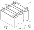
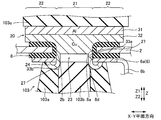
- the assembled battery 100 is a large-scale battery system used in an electric vehicle (EV, electric vehicle), a hybrid vehicle (HEV, hybrid electric vehicle), a residential power storage system, and the like. As shown in FIG. 1, the assembled battery 100 is configured by connecting a plurality of lithium ion batteries 1 electrically by a plurality of flat plate-shaped bus bars 101 (shown by a dotted line).
- a plurality of lithium ion batteries 1 are arranged so as to be arranged along the lateral direction (X direction) of the lithium ion battery 1 when viewed in a plane.
- the positive electrode terminal 10 is located on one side (Y1 side) of the longitudinal direction (Y direction) orthogonal to the lateral direction when viewed in a plane, and is located on the other side (Y2 side) of the Y direction.
- the lithium ion battery 1 (1a) in which the negative electrode terminal 20 is located and the lithium ion battery 1 (1b) in which the positive electrode terminal 10 is located on the Y2 side and the negative electrode terminal 20 is located on the Y1 side are arranged along the X direction. They are arranged alternately.
- the negative electrode terminal 20 of the predetermined lithium ion battery 1 and the positive electrode terminal 10 of the lithium ion battery 1 adjacent to the predetermined lithium ion battery 1 are X of the bus bar 101 composed of pure Al extending in the X direction. It is joined by resistance welding to one end in the direction. As a result, the negative electrode terminal 20 of the lithium ion battery 1 is connected to the positive electrode terminal 10 of the adjacent lithium ion battery 1 via the bus bar 101. In this way, the assembled battery 100 in which a plurality of lithium ion batteries 1 are connected in series is configured.
- the bus bar 101 made of pure Al By using the bus bar 101 made of pure Al, the weight of the bus bar 101 can be reduced as compared with the case of using the bus bar made of pure Cu. Therefore, by using the bus bar 101 made of pure Al, it is possible to reduce the weight of the entire assembled battery 100 using the plurality of bus bars 101.
- pure Al means, for example, A1000 series aluminum specified in JIS standard.
- pure Cu means, for example, oxygen-free copper, tough pitch copper, or C1000 series copper specified in JIS standards such as phosphorus deoxidized copper.
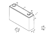
- the lithium ion battery 1 has a substantially rectangular parallelepiped appearance. Further, the lithium ion battery 1 has a lid member 2 arranged on one side (Z1 side) in the vertical direction (Z direction) orthogonal to the X direction and the Y direction, and a battery case arranged on the other side (Z2 side). It has a main body 3. The lid member 2 and the battery case body 3 are both made of Ni-plated steel plate.
- the lid member 2 is formed in a flat plate shape. Further, the lid member 2 is provided with a pair of insertion holes 2a and an insertion hole 2b so as to penetrate in the Z direction. The pair of insertion holes 2a and the insertion holes 2b are formed at predetermined intervals in the Y direction of the lid member 2, and are formed substantially in the center of the lid member 2 in the X direction. Further, the positive electrode terminal 10 and the negative electrode terminal 20 are configured to be inserted into the pair of insertion holes 2a and the insertion holes 2b, respectively.
- the lithium ion battery 1 includes a power generation element 4 in which a positive electrode 4a, a negative electrode 4b, and a separator 4c are laminated in a roll shape, and an electrolytic solution (not shown).
- the positive electrode 4a is composed of an Al foil coated with a positive electrode active material.
- the negative electrode 4b is composed of a Cu foil coated with a negative electrode active material.
- the separator 4c has a function of insulating the positive electrode 4a and the negative electrode 4b.
- the lithium ion battery 1 has a positive electrode current collector 5 that electrically connects the positive electrode terminal 10 and the positive electrode 4a of the power generation element 4, and a negative electrode that electrically connects the negative electrode terminal 20 and the negative electrode 4b of the power generation element 4. It is provided with a current collector 6.
- the positive electrode current collector 5 is arranged on the Y1 side so as to correspond to the positive electrode terminal 10. Further, the positive electrode current collector 5 connects the connecting portion 5a in which the hole portion 5d into which the positive electrode terminal 10 is inserted is formed, the leg portion 5b extending toward the Z2 side, the leg portion 5b, and the plurality of positive electrodes 4a. Includes plate 5c. Further, the positive electrode current collector 5 is composed of pure Al like the positive electrode 4a.
- the negative electrode current collector 6 is arranged on the Y2 side so as to correspond to the negative electrode terminal 20. Further, the negative electrode current collector 6 connects the connecting portion 6a in which the hole 6d into which the negative electrode terminal 20 is inserted, the leg portion 6b extending to the Z2 side, the leg portion 6b, and the plurality of negative electrodes 4b are connected. Includes plate 6c. Further, the negative electrode current collector 6 is made of pure Cu like the negative electrode 4b.
- the seal member 7 is formed with a hole 7a into which the positive electrode terminal 10 is inserted.
- the seal member 7 suppresses contact between the upper surface of the lid member 2 on the Z1 side and the inner surface of the insertion hole 2a with the positive electrode terminal 10, and also suppresses contact between the lower surface of the lid member 2 on the Z2 side and the positive electrode current collector 5. It is arranged so as to prevent contact with.
- the seal member 8 is formed with a hole 8a into which the negative electrode terminal 20 is inserted.
- the seal member 8 suppresses contact between the upper surface of the lid member 2 on the Z1 side and the inner surface of the insertion hole 2b with the negative electrode terminal 20, and also with the lower surface of the lid member 2 on the Z2 side and the negative electrode current collector 6. Is arranged so as to prevent contact with each other.
- the positive electrode terminal 10 has a columnar shaft portion 11 extending in the Z direction and an end portion of the shaft portion 11 on the Z1 side in the X direction and the Y direction (XY plane direction) from the shaft portion 11. ) Has an annular flange portion 12 formed so as to have a radial spread.
- the shaft portion 11 is configured to be located substantially at the center of the positive electrode terminal 10 in the X direction and the Y direction.
- the positive electrode terminal 10 is made of pure Al, like the positive electrode current collector 5 and the bus bar 101. Further, the positive electrode terminal 10 has a recess 13 formed at the end of the shaft portion 11 on the Z2 side. Further, the positive electrode terminal 10 is a wall forming a recess 13 in a state where the shaft portion 11 is inserted into the insertion hole 2a of the lid member 2 (hole portion 7a of the seal member 7) and the hole portion 5d of the positive electrode current collector 5. The portion is used to crimp the positive electrode current collector 5 (see FIG. 3), and in the crimped state, the positive electrode current collector 5 is joined and fixed by laser welding. The positive electrode terminal 10 having the shaft portion 11, the flange portion 12, and the recess 13 is formed by pressing an Al plate material (not shown).
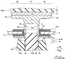
- the negative electrode terminal 20 has a columnar shaft portion 21 extending in the Z direction and an end portion of the shaft portion 21 on the Z1 side in the X direction and the Y direction (X-) from the shaft portion 21. It has an annular flange portion 22 when viewed from the Z direction, which is formed so as to have a radial spread in the Y plane direction).
- the shaft portion 21 is configured to be located substantially at the center of the negative electrode terminal 20 in the X direction and the Y direction.
- the negative electrode terminal 20 is an example of a "battery terminal" in the claims.
- the XY plane direction is an example of the "radiation direction" of the claims.
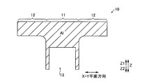
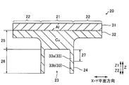
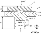
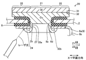
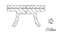
- the negative electrode terminal 20 has a T-shape in which the shaft portion 21 projects from the Al layer 31 side to the Cu layer 32 side, or has a cross shape as shown in FIG.
- the negative electrode terminal 20 has a first shaft portion 21a in which the shaft portion 21 projects from the Al layer 31 side to the Cu layer 32 side and a length in which the shaft portion 21 projects and extends toward the Cu layer 32 side. It has a second shaft portion 21b that protrudes toward the Al layer 31 with a protrusion length t2 that is smaller than t1.
- the bus bar 101 may be connected to the second shaft portion 21b of the negative electrode terminal 20 having a cross shape.
- the shaft portion 21 composed of the Cu layer 32 includes a solid region 25 adjacent to the Al layer 31 and a hollow region 26 including a recess 23 and a wall portion 24 surrounding the recess 23. It has.
- the wall portion 24 is formed so as to extend from the tip of the solid region 25 of the shaft portion 21 on the Z2 side (Cu layer side).
- the region from the base portion (root) in contact with the solid region 25 to the center of the wall portion 24 in the Z2 direction is particularly designated as the base region 27.
- the recess 23 is formed in an annular shape like a round pipe cross section when viewed from the Z2 side.
- the Z2 side of the shaft portion 21 on which the recess 23 is formed is formed so as to have a cylindrical shape. That is, the recess 23 is formed in a region surrounded by a cylindrical wall portion 24 on the outside.
- the Vickers hardness of the Cu portion 33 (particularly the Cu portion 33a of the base region 27) in the wall portion 24 is preferably 110 HV or more and 125 HV or less. Further, the Vickers hardness of the Cu portion 33 (particularly the Cu portion 33a) is more preferably 114 HV or more and 125 HV or less from the viewpoint of making it difficult for cracks to occur when an external force such as vibration is applied to the crimped Cu portion 33. Even more preferably, it is 118 HV or more and 125 HV or less.
- the Vickers hardness is determined by the size of the area of the indentation (indentation) formed at that time when a rigid body (indenter) made of diamond is pressed against the test object.
- the negative electrode terminal 20 having a Vickers hardness of 110 HV or more and 125 HV or less of the Cu portion 33 can have mechanical properties suitable for bending and crimping the Cu portion 33, and the crimped Cu portion 33 vibrates or the like. It has appropriate mechanical properties that cracks are unlikely to occur when an external force is applied. Specifically, when the Cu portion 33 having a Vickers hardness of more than 125 HV is bent and crimped, cracks are likely to occur in the Cu portion. Further, if a Cu portion having a Vickers hardness of less than 110 HV is bent and crimped, cracks are likely to occur when an external force such as vibration is applied to the Cu portion.
- the Cu portion 33 of the negative electrode terminal 20 has an appropriate Vickers hardness of 110 HV or more and 125 HV or less, the negative electrode terminal is caused by an external force such as vibration being applied during the use of the assembled battery 100 (lithium ion battery 1). Cracks are less likely to occur in the Cu portion 33 of 20.
- the Vickers hardness is measured at the Cu portion 33 of the wall portion 24 (preferably the Cu portion 33a of the base region 27).
- the base region 27 of the wall portion 24 is a portion where cracks are most likely to occur when the Cu portion 33 of the wall portion 24 is bent and crimped. If the base region 27 of the wall portion 24 is cracked, good connection between the negative electrode terminal 20 and another member (negative electrode current collector 6) cannot be made. Therefore, the Cu portion of the base region 27 of the wall portion 24 33a is a particularly important part. Therefore, it is preferable to measure the Vickers hardness of the Cu portion 33a of the base region 27 of the wall portion 24.
- the Cu portion 33a of the base region 27 of the wall portion 24 and the Cu portion 33b other than the base region 27 of the wall portion 24 are both made of the same material as the Cu layer 32, and the flange portion 22 extends in the direction (X-).
- the thickness in the Y plane direction) is the same. Therefore, it is considered that the Vickers hardness of the Cu portion 33a of the base region 27 of the wall portion 24 and the Vickers hardness of the Cu portion 33b other than the base region 27 of the wall portion 24 are substantially the same. Therefore, the Vickers hardness of the Cu portion 33 of the wall portion 24 can be obtained by measuring the Vickers hardness of the Cu portion 33a of the base region 27 of the wall portion 24.
- the cross-sectional area of the Cu crystal grains (for example, Cu crystal grains 34) of the Cu portion 33 (particularly the Cu portion 33a of the base region 27) composed of the Cu layer 32 of the wall portion 24 is 10 ⁇ m 2. It is 100 ⁇ m 2 or less.
- the cross-sectional area of the Cu crystal grains of the Cu portion 33a of the wall portion 24 is 10 ⁇ m 2 or more and 100 ⁇ m 2 or less, the wall portion 24 is bent and crimped to be fixed to another member (negative electrode current collector 6). It can have suitable mechanical properties and can have appropriate mechanical properties to maintain its fixed state (caulked state).
- the cross-sectional area of the Cu crystal grains of the Cu portion 33 of the wall portion 24 is 10 ⁇ m 2 or more and 100 ⁇ m 2 or less, cracks occur when the wall portion 24 is bent and crimped. In addition to being difficult to do, cracking is unlikely to occur when an external force such as vibration is applied after the wall portion 24 is fixed to another member (negative electrode current collector 6) by bending and crimping.
- the Cu portion 33 of the wall portion 24 cross-sectional area (especially Cu portions 33a of the base region 27) of the Cu crystal grains e.g. Cu crystal grains 34
- the Cu crystal grains e.g. Cu crystal grains 34
- the area of the Cu crystal grains constituting the Cu portion 33a becomes smaller, the Vickers hardness of the Cu portion 33a tends to increase.
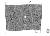
- the cross-sectional area of the Cu crystal grains (for example, Cu crystal grains 34) of the Cu portion 33 is measured using an electron microscope in the cross section of the wall portion 24 cut in the extending direction (Z direction) of the shaft portion 21.
- the cross-sectional area of the Cu crystal grains (for example, Cu crystal grains 34) of the Cu portion 33 is preferably measured in the base region 27 of the wall portion 24.
- the cross-sectional area of the Cu crystal grains of the Cu portion 33 may be a value obtained from the electron microscope image of the Cu portion 33 to be measured by using a general electron microscope and a general image analysis system attached thereto. Specifically, for example, under an electron microscope, a contour (grain boundary) enhancement process (for example, a process of drawing a contour line of a Cu crystal grain 34) of Cu crystal grains (for example, Cu crystal grain 34) constituting the Cu portion 33 is performed. Then, the area within the contour (grain boundary) is taken as the cross-sectional area of the Cu crystal grain (for example, Cu crystal grain 34).
- Such a process for determining the cross-sectional area of Cu crystal grains was carried out with arbitrary and a plurality of Cu crystal grains in an electron microscope image of the Cu portion 33 of the wall portion 24 (preferably the Cu portion 33a of the base region 27), and the obtained plurality of Cu crystal grains were obtained.
- the average value obtained by dividing the total cross-sectional area of the Cu crystal grains by the number of Cu crystal grains is obtained, and is used as the cross-sectional area (average cross-sectional area) of the Cu crystal grains of the Cu portion 33 in the electron microscope image.
- the Cu crystal grains (for example, Cu crystal grains 34) of the Cu portion 33 composed of the Cu layer 32 of the base region 27 of the wall portion 24 are substantially needle-shaped with an extremely large aspect ratio by press working. It was discovered that it would be in the form of. Therefore, in the present embodiment, the above-mentioned cross-sectional area (average cross-sectional area) is adopted instead of the general particle size (circle-equivalent diameter) as an index indicating the Cu crystal grains of the Cu portion 33 (Cu portion 33a). ..
- the Cu portion 33 of the wall portion 24 (preferably the Cu portion 33a of the base region 27), for example, an electron microscope image of a region containing Cu crystal grains 34 is acquired, and the Cu crystal grains in this region are obtained.
- the cross-sectional area (average cross-sectional area) S2 is obtained, and the cross-sectional area (average cross-sectional area) S1 of the Cu crystal grains constituting the Cu material 320 (see FIG. 10) of the clad material before press processing is used to obtain the Cu portion 33 (Cu).
- the deformation rate D of the Cu crystal grains before and after the press processing of the portion 33a) is obtained by the following formula 1.
- the deformation rate D is 0% when the cross-sectional areas of Cu crystal grains before and after press working of the Cu portion 33 are the same.
- the deformation ratio D is such that the cross-sectional area S2 of the Cu crystal grains of the Cu portion 33 after the press working is smaller than the cross-sectional area S1 of the Cu crystal grains of the Cu material 320 (see FIG. 10) before the press working (S2 ⁇ S1). ), 0% ⁇ D ⁇ 100% is satisfied. Therefore, it means that the Cu crystal grains of the Cu portion 33 after the press working are deformed to be smaller than the Cu crystal grains of the Cu material 320 before the press working as the deformation rate D becomes larger.
- the hardness of the Cu portion 33 after the press working is higher than the hardness of the Cu material 320 before the press working due to the work hardening caused by the press working. Can also be increased.
- the Cu crystal grains of the Cu portion 33b other than the base region 27 of the wall portion 24 also have a smaller cross-sectional area. Conceivable.
- the deformation rate D of the Cu crystal grains before and after the press working of the Cu portion 33 is preferably 45% or more, more preferably 60% or more.
- the negative electrode terminal 20 is recessed in a state where the shaft portion 21 is inserted into the insertion hole 2b of the lid member 2 (hole 8a of the seal member 8) and the hole 6d of the negative electrode current collector 6.
- the wall portion 24 forming the 23 is bent and crimped to the negative electrode current collector 6, and further joined to and fixed to the negative electrode current collector 6 by laser welding.
- the shape of the recess 23 as viewed from the Z2 direction side is not particularly limited, but may be, for example, a rounded rectangle having four rounded corners, such as a circle, an ellipse, and a rectangle.
- the negative electrode terminal 20 is manufactured by pressing the clad material 300.
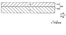
- the clad material 300 is a state in which an Al plate material 131 made of pure Al or an Al-based alloy (see FIG. 12) and a Cu plate material 132 made of pure Cu or a Cu-based alloy (see FIG. 12) are laminated in the Z direction.
- a clad material 300 having a two-layer structure composed of an Al material 310 and a Cu material 320 By being rolled and joined, it is formed by using a clad material 300 having a two-layer structure composed of an Al material 310 and a Cu material 320.
- the Al plate member 131 and the Cu plate material 132 that have been rolled (clad-rolled) and joined are subjected to further appropriate heat treatment and are atomically (chemically) joined.
- the clad material 300 having a two-layer structure of the Al material 310 made of the Al plate material 131 and the Cu material 320 made of the Cu plate material 132 is pressed with a large deformation performed to produce the negative electrode terminal 20. It can have sufficient bonding strength to withstand processing.
- the Al material 310 of the clad material 300 corresponds to the Al layer 31 of the negative electrode terminal 20.
- the pure Al constituting the Al material 310 of the clad material 300 that is, the Al layer 31 of the negative electrode terminal 20
- about 99% by mass or more of Al such as A1050 (JIS standard), A1100 (JIS standard), and A1200 (JIS standard) is used. It is possible to use pure Al or the like.
- A5000 series (JIS standard) such as A5052 may be used, and A3000 series (JIS standard) or the like can also be used.
- the Cu material 320 of the clad material 300 corresponds to the Cu layer 32 and the Cu portion 33 of the negative electrode terminal 20.
- the pure Cu constituting the Cu material 320 of the clad material 300 that is, the Cu layer 32 and the Cu portion 33 of the negative electrode terminal 20
- so-called oxygen-free copper, phosphor deoxidized copper, tough pitch copper, etc. of the C1000 series (JIS standard) are used. It may be used, and C1510 (JIS standard) to which a small amount of Zr is added in order to suppress the coarsening of crystals can also be used.
- C2000 series JIS standard
- C2600 can be used as the Cu-based alloy.
- the Cu crystal grains of the Cu material 320 constituting the clad material 130 are work-hardened by press working performed to produce the negative electrode terminal 20. Therefore, the Vickers hardness of the Cu material 320 constituting the clad material 130 is preferably 70 HV or less. When the Vickers hardness of the Cu material 320 of the clad material 300 is 70 HV or less on the cut surface in the thickness direction of the clad material 300, the workability during press working is appropriately improved.
- the cross-sectional area of the Cu crystal grains (for example, Cu crystal grains 34) constituting the Cu portion 33 can be formed to an appropriate size, and the Cu portion 33 has an appropriate hardness, for example, a Vickers hardness of 110 HV or more and 125 HV or less. Can be formed into.
- the cross-sectional area of the Cu crystal grains (for example, Cu crystal grains 340) constituting the Cu material 320 is preferably 40 ⁇ m 2 or more on the cut surface along the thickness direction (Z direction) of the clad material 300. It is 750 ⁇ m 2 or less, more preferably 40 ⁇ m 2 or more and 500 ⁇ m 2 or less.
- the deformation ratio D is 45% or more and 100% by using the clad material 300 in which the cross-sectional area of the Cu crystal grains constituting the Cu material 320 is preferably 40 ⁇ m 2 or more and 750 ⁇ m 2 or less, more preferably 40 ⁇ m 2 or more and 500 ⁇ m 2 or less.
- the Cu crystal grains of the Cu portion 33 of the wall portion 24 of the negative terminal terminal 20 after the press working as shown in FIGS. 6 and 7 are 10 ⁇ m 2 or more and 100 ⁇ m. 2 following appropriate cross-sectional area (preferably 10 [mu] m 2 or more 65 .mu.m 2 or less, more preferably 10 [mu] m 2 or more 40 [mu] m 2 or less) is likely to be formed on. If the cross-sectional area of the Cu crystal grains of the Cu material 320 before the press working is less than 40 ⁇ m 2 , the Cu material 320 becomes difficult to press.
- the Cu material 320 When the cross-sectional area of the Cu crystal grains of the Cu material 320 before the press working exceeds 750 ⁇ m 2 , the Cu material 320 has the cross-sectional area of the Cu crystal grains of the Cu portion 33 of the wall portion 24 after the press working of 100 ⁇ m 2 or less. It becomes difficult to increase the hardness of the Cu portion 33.
- the cross-sectional area of the Cu crystal grains (for example, Cu crystal grains 340) constituting the Cu material 320 is the cross-sectional area of the Cu crystal grains (for example, Cu crystal grains 34) of the Cu portion 33 of the wall portion 24 of the negative electrode terminal 20. Similarly, it can be obtained by the above-mentioned method for obtaining the average cross-sectional area of Cu crystal grains.
- an Al plate material 131 made of pure Al or an Al alloy and a Cu plate material 132 made of pure Cu or a Cu alloy are prepared.
- the ratio of the thickness of the Al plate 131 to the thickness of the Cu plate 132 is substantially the same as the ratio of the thickness of the Al layer 31 and the Cu layer 32 constituting the flange portion 22 of the negative electrode terminal 20 (see FIG. 6) in the Z direction.
- the thickness of the Al plate member 131 may be the same as the thickness of the Cu plate member 132.
- the thickness of the Cu plate member 132 may be larger than that of the Al plate material 131 depending on the size of the shaft portion 21 of the negative electrode terminal 20 after press working (the amount of protrusion toward the Z2 side, the shaft diameter) and the like. Further, in order to bring the workability of the Cu plate material 132 during clad rolling closer to the workability of the Al plate material 131, the Cu plate material 132 before clad rolling may be subjected to tempering treatment such as temper rolling and softening annealing.
- a strip-shaped clad material 130 having a two-layer structure is produced in which the Al plate material 131 and the Cu plate material 132 are joined in a laminated state in the thickness direction.
- the longitudinal direction of the strip-shaped Al plate 131 and the strip-shaped Cu plate 132 becomes the rolling direction.
- a strip-shaped clad material 130 is produced in which the Al plate material 131 and the Cu plate material 132 are laminated to each other (rolling joint) in a state of being laminated in the thickness direction.
- the number of clad rolling passes can be appropriately selected.
- diffusion annealing is performed by holding the clad material 130 in a predetermined atmosphere and an environment of a holding temperature at which the Al plate material 131 does not melt using an annealing furnace 50 for a predetermined time. I do.
- the holding temperature is, for example, a temperature lower than the melting point of the Al plate 131.
- the clad material 130 has a sufficiently higher bonding strength between the Al plate material 131 and the Cu plate material 132 than the bonding strength of the plating film. Further, if necessary, finish rolling, shape correction, softening annealing at a holding temperature at which the Al plate material 131 does not melt, or the like may be performed. Then, using the strip-shaped clad material 130, the individual piece-shaped clad material 300 having a two-layer structure as shown in FIG. 10 suitable for press working to form the negative electrode terminal 20 as shown in FIGS. 6 and 7.
- an individual piece-shaped clad material 300 is produced in which the Al material 310 and the Cu material 320 are bonded in a laminated state in the thickness direction.
- the piece-shaped clad material 300 is manufactured, for example, after slitting the clad material 130.
- the step of producing the clad material 130 is preferable in the cut surface in the thickness direction (Z direction) of the individual clad material 300 when the individual clad material 300 is formed by using the strip-shaped clad material 130.
- the Vickers hardness of the Cu material 320 is 70 HV or less, and the cross-sectional area of the Cu crystal grains constituting the Cu material 320 is preferably 40 ⁇ m 2 or more and 750 ⁇ m 2 or less, more preferably 40 ⁇ m 2 or more and 500 ⁇ m. It is advisable to perform rolling and diffusion annealing so as to be 2 or less, and if necessary, perform finish rolling, shape correction, softening annealing and the like.
- the negative electrode terminal 20 shown in FIG. 6 is formed by using the individual piece-shaped clad material 300 in which the Al material 310 and the Cu material 320 are laminated in the thickness direction.
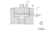
- the individual piece-shaped clad material 300 is pressed. Specifically, first, the individual piece-shaped clad material 300 is arranged in the cavity 41b of the die 41a of the press processing machine 41.
- the cavity 41b of the mold 41a has a cavity shape corresponding to, for example, the shaft portion 21, the flange portion 22, and the recess 23 of the negative electrode terminal 20 shown in FIG.
- the clad material 300 is pressed by applying pressure from the Z1 side. By this press working, the Cu material 320 of the clad material 300 is moved into the cavity 41b on the Z2 side corresponding to the shaft portion 21.
- the cross-sectional area of the Cu crystal grains constituting the Cu portion 33 of the wall portion 24 (particularly the Cu portion 33a of the base region 27) in the negative electrode terminal 20 after the press working is preferably 10 ⁇ m 2 or more and 100 ⁇ m 2 or less.
- the cross-sectional area of the Cu crystal grains constituting the Cu material 320 is set to S1 on the cut surface in the thickness direction of the clad material 300, and the shaft portion 21 is cut in the axial direction (Z direction).
- the deformation rate D of the Cu crystal grains before and after press working which is obtained by (S1-S2) / S1 ⁇ 100, is more preferably 45% or more. Is 60% or more, and the clad material 300 is press-processed.
- the Vickers hardness of the Cu portion 33 is 110 HV or more and 125 HV or less, which is preferable, or 114 HV or more on the cut surface of the shaft portion 21 in the axial direction (Z direction).
- the clad material 300 is press-processed so as to have a more preferable Vickers hardness of 125 HV or less, and further to have a more preferable Vickers hardness of 118 HV or more and 125 HV or less.
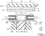
- a lid member 2 in which the seal member 8 is fitted into the insertion hole 2b is prepared. Then, the connecting portion 6a of the negative electrode current collector 6 is brought into contact with the Z2 side surface of the sealing member 8. In this state, the fixing member 103a of the caulking jig 103 is brought into contact with the surface of the negative electrode current collector 6 on the Z2 side to be fixed. In that state, the rod-shaped member 103b of the caulking jig 103 is inserted into the insertion hole 2b (hole portion 8a of the seal member 8) from the Z2 side. Then, the end portion of the inserted rod-shaped member 103b on the Z1 side is fitted into the recess 23 of the negative electrode terminal 20.
- the negative electrode terminal 20 is pressed from the Z1 side toward the Z2 side by the pressing member 103c of the caulking jig 103.
- the negative electrode terminal 20 is moved to the Z2 side together with the rod-shaped member 103b.
- the negative electrode terminal 20 is moved by the pressing force of the pressing member 103c until the end portion of the wall portion 24 on the Z2 side is located on the Z2 side of the insertion hole 2b.
- the negative electrode terminal 20 is moved to the Z2 side while the Cu portion 33 of the cylindrical wall portion 24 is deformed along the outer peripheral surface of the rod-shaped member 103b.
- the negative electrode terminal 20 is moved to the Z2 side while the Cu portion 33 of the cylindrical wall portion 24 is further deformed along the concave surface on the Z1 side of the fixing member 103a of the caulking jig 103.
- the movement of the rod-shaped member 103b is stopped.
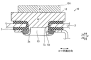
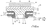
- the wall portion 24 of the negative electrode terminal 20 is bent so as to have a semicircular cross section as shown in FIG.
- the negative electrode terminal 20 is crimped to the negative electrode current collector 6 by the Cu portion 33 of the wall portion 24 that is radially bent in the XY plane direction.
- the negative electrode terminal 20 in the crimped state and the negative electrode current collector 6 are welded by laser welding. Specifically, the tip end side portion of the wall portion 24 bent radially in the XY plane direction of the negative electrode terminal 20 is annularly welded to the connection portion 6a of the negative electrode current collector 6 to be joined. As shown in FIG. 9, the tip of the wall portion 24 on the Z2 side of the negative electrode terminal 20 on the side to be welded to the negative electrode current collector 6 of the lithium ion battery 1 is joined to the negative electrode current collector 6.
- the negative electrode terminal 20 has a shaft portion 21 extending from the Al layer 31 side to the Cu layer 32 side, a flange portion 22 extending in the radial direction from the side of the shaft portion 21, and the Cu layer 32 side of the shaft portion 21.
- the cross-sectional area of Cu crystal grains constituting the Cu portion 33 composed of the Cu layer 32 of the wall portion 24 on the axially cut surface of the shaft portion 21 is provided with the recess 23 surrounded by the wall portion 24 further extending from the tip of the wall portion 24. Is 10 ⁇ m 2 or more and 100 ⁇ m 2 or less.
- the cross-sectional area of the Cu crystal grains constituting the Cu portion 33 composed of the Cu layer 32 of the wall portion 24 is 10 ⁇ m 2 or more and 100 ⁇ m 2 or less, so that the shaft portion 21 Since the Cu portion 33 at the tip of the head has an appropriate Vickers hardness, sufficient workability can be obtained. Therefore, by bending and crimping the Cu portion 33 (Cu portion 33b) at the tip of the shaft portion 21, it is possible to have appropriate mechanical properties for fixing to another member, and the fixed state (caulking state). Can have suitable mechanical properties to maintain.
- the Cu portion 33 (Cu portion 33b) is bent. And mechanical properties that can withstand caulking are required.
- the Cu portion 33 having a cross-sectional area of 10 ⁇ m 2 or more and 100 ⁇ m 2 or less of Cu crystal grains can have a mechanical property of withstanding bending and caulking, that is, cracking is unlikely to occur when bent and crimped.
- mechanical characteristics for maintaining the fixed state in the crimped Cu portion 33 (Cu portion 33b) are required. Be done.
- the Cu portion 33 (Cu portion 33b) having a cross-sectional area of 10 ⁇ m 2 or more and 100 ⁇ m 2 or less of Cu crystal grains is cracked when an external force such as vibration is applied after being fixed to another member by bending and crimping. It can have a mechanical property that it is difficult to withstand the fixed state over time.
- the cross-sectional area of the Cu crystal grains constituting the Cu portion 33 is 65 ⁇ m 2 or less.
- the cross-sectional area of the Cu crystal grains constituting the Cu portion 33 (10 [mu] m 2 or more) by 65 ⁇ m 2 or less, to improve the processability of the tip of the Cu portion 33 of the shaft portion 21 (Cu portion 33b) Therefore, by bending and crimping the Cu portion 33 at the tip of the shaft portion 21, it is possible to have more appropriate mechanical properties by fixing it to another member, and the fixed state (caulked state) is maintained. Can have sufficient and appropriate mechanical properties for this purpose.
- the cross-sectional area of the Cu crystal grains constituting the Cu portion 33 is 40 ⁇ m 2 or less (10 ⁇ m 2 or more).
- the cross-sectional area of the Cu crystal grains constituting the Cu portion 33 is 40 ⁇ m 2 or less, the workability of the Cu portion 33 (Cu portion 33b) at the tip of the shaft portion 21 can be further improved.
- the Cu portion 33 (Cu portion 33b) at the tip of the shaft portion 21 can be bent and crimped to be fixed to another member, so that it can have more suitable mechanical properties. , It can have more suitable mechanical properties to maintain its fixed state (caulked state).
- the Vickers hardness of the Cu portion 33 is 110 HV or more and 125 HV or less.
- the Cu portion 33 at the tip of the shaft portion 21 has an appropriate Vickers hardness, it is possible to have mechanical properties suitable for bending and crimping the Cu portion 33 at the tip of the shaft portion 21. It is possible to have appropriate mechanical properties in which cracks are unlikely to occur when an external force such as vibration is applied to the crimped Cu portion 33.
- the method for manufacturing the negative electrode terminal 20 according to the present embodiment is a Cu crystal forming a Cu portion 33 (particularly the Cu portion 33a of the base region 27) composed of the Cu layer 32 of the wall portion 24 on the axially cut surface of the shaft portion 21.
- the step of pressing the clad material 300 so that the cross-sectional area of the grains is 10 ⁇ m 2 or more and 100 ⁇ m 2 or less is included.
- the Cu portion 33 composed of the Cu layer 32 of the wall portion 24 can be press-processed so as to have sufficient hardness. Therefore, the Cu portion 33 has sufficient workability, and other members can be bent and crimped.
- a Cu portion 33 having mechanical properties suitable for fixing to can be formed at the tip of the shaft portion 21, and a Cu portion having suitable mechanical properties for maintaining the fixed state (caulking state). 33 can be formed. Specifically, in order to fix the Cu portion 33 at the tip of the shaft portion 21 of the negative electrode terminal 20 to another member by bending and crimping, the Cu portion 33 to be bent (particularly the Cu portion 33a of the base region 27). In addition, mechanical properties that can withstand bending and caulking are required.
- Cu portion 33 which is press-processed to the cross-sectional area of Cu crystal grains is 10 [mu] m 2 or more 100 [mu] m 2 or less, that crack is unlikely to occur when tightening Teka bent, have mechanical properties to withstand the bending and caulking Can be done. Further, in order to maintain a sound fixed state (caulked state) between the negative electrode terminal 20 and another member, the crimped Cu portion 33 is required to have a mechanical property of maintaining the fixed state.
- the step of forming the negative electrode terminal 20 includes a step of pressing the clad material 300 so that the cross-sectional area of the Cu crystal grains constituting the Cu portion 33 is 40 ⁇ m 2 or less.
- the cross-sectional area of the Cu crystal grains constituting the Cu portion 33 (10 [mu] m 2 or more) 65 .mu.m 2 by pressing a clad material 300 to be less than, the processability of the tip of the Cu portion 33 of the shaft portion 21
- the clad material 300 can be press-processed so as to improve the pressure, the Cu portion having more suitable mechanical properties can be fixed to another member by bending and crimping the Cu portion 33 at the tip of the shaft portion 21. 33 can be formed.
- the Cu portion 33 can further suppress the occurrence of cracks when bent and crimped, and cracks occur when an external force such as vibration is applied to the crimped Cu portion 33. It can be sufficiently suppressed.
- the step of forming the negative electrode terminal 20 includes a step of pressing the clad material 300 so that the cross-sectional area of the Cu crystal grains constituting the Cu portion 33 is 40 ⁇ m 2 or less.
- the clad material 300 is press-processed so that the cross-sectional area of the Cu crystal grains constituting the Cu portion 33 is (10 ⁇ m 2 or more) 40 ⁇ m 2 or less, so that the Cu portion 33 at the tip of the shaft portion 21 is workable.
- the clad material 300 can be press-processed so as to further improve the pressure, Cu having more suitable mechanical properties can be fixed to other members by bending and crimping the Cu portion 33 at the tip of the shaft portion 21. Part 33 can be formed.
- the Cu portion 33 can sufficiently suppress the occurrence of cracks when bent and crimped, and cracks occur when an external force such as vibration is applied to the crimped Cu portion 33. Can be sufficiently suppressed.
- the cross-sectional area of the Cu crystal grains constituting the Cu material 320 is S1 on the cut surface in the thickness direction of the clad material 300, and the cut surface in the axial direction of the shaft portion 21.
- the deformation rate of the Cu crystal grains before and after the press working obtained by (S1-S2) / S1 ⁇ 100 is 45% or more and less than 100%.
- the step of forming the recess 23 is included.
- the Cu portion 33 having a smaller cross-sectional area of Cu crystal grains than the Cu material 320 of the clad material 300 before press working is formed. can do.
- the cross-sectional area of the Cu crystal grains constituting the Cu portion 33 is formed to be small, mechanical properties such as elongation are improved, and cracks are suppressed from occurring when the Cu portion 33 is bent and crimped. At the same time, it is possible to suppress the occurrence of cracks when an external force such as vibration is applied to the crimped Cu portion 33.
- the step of forming the negative electrode terminal 20 includes a step of forming the recess 23 so that the deformation rate is 60% or more (less than 100%).
- the cross-sectional area of Cu crystal grains is smaller than that of the Cu material 320 of the clad material 300 before press working, and the Cu portion 33 Can be formed.
- the cross-sectional area of the Cu crystal grains constituting the Cu portion 33 is formed to be smaller, mechanical properties such as elongation are further improved, and cracks occur when the Cu portion 33 is bent and crimped. It can be sufficiently suppressed, and cracks can be sufficiently suppressed when an external force such as vibration is applied to the crimped Cu portion 33.
- the clad material 300 is formed so that the Vickers hardness of the Cu material 320 is 70 HV or less on the cut surface in the thickness direction (Z direction) of the clad material 300. Including the process. As a result, since the Vickers hardness of the Cu material 320 of the clad material 300 is 70 HV or less, the workability during press working is appropriately improved, and the cross-sectional area of the Cu crystal grains constituting the Cu portion 33 after press working is suitable. The Cu portion 33 after press working can be formed to have an appropriate Vickers hardness.
- the step of forming the negative electrode terminal 20 includes a step of pressing the clad material 300 so that the Vickers hardness of the Cu portion 33 is 110 HV or more and 125 HV or less.
- Example 1 The clad material 300 of Examples (No. 1 to No. 20) was produced in the same manner as in the production method of the above embodiment. At that time, the clad material 130 is produced by clad rolling and diffusion annealing as shown in FIG. 12, and the clad material 300 having a two-layer structure as shown in FIG. 10 is pressed from the clad material 130 to the negative electrode terminal. It was made to have a predetermined shape suitable for 20.
- the produced clad material 300 constitutes a Cu material 320 on the cut surface in the thickness direction (Z direction) of the clad material 300 by using the area measurement function attached to a digital microscope (VHX-5000 manufactured by KEYENCE CORPORATION). The cross-sectional area of the Cu crystal grains was measured. The measurement results are shown in Table 1.
- the Vickers hardness of the Cu material 320 was measured on the cut surface in the thickness direction (Z direction) of a plurality of clad materials 300 arbitrarily selected from the produced clad materials 300, for example, 58HV, 60HV, 67HV and the like were obtained.
- the range was 58 HV or more and 67 HV or less, and the average value was 61.7 HV.
- the Vickers hardness measurement method was in accordance with JIS Z2244: 2009 (load 0.49N).
- the cross-sectional area of the Cu crystal grains constituting the Cu portion 33 composed of the Cu layer 32 of the wall portion 24 of the negative electrode terminal 20 is 10 ⁇ m 2 or more and 100 ⁇ m 2 or less, preferably 10 ⁇ m 2 or more and 65 ⁇ m 2. or less, more preferably adjusted to within a range of 10 [mu] m 2 or more 40 [mu] m 2 or less.
- the manufactured negative electrode terminal 20 uses the area measurement function attached to a digital microscope (VHX-5000 manufactured by KEYENCE CORPORATION) to obtain Cu on the cut surface of the shaft portion 21 of the negative electrode terminal 20 in the axial direction (Z direction).
- the cross-sectional area of the Cu crystal grains constituting the portion 33 (Cu portion 33a) was measured. The measurement results are shown in Table 1.
- the Vickers hardness of the Cu material 320 was measured on the cut surface of the shaft portion 21 of the negative electrode terminal 20 of 30 in the axial direction (Z direction).
- the Vickers hardness measurement method was in accordance with JIS Z2244: 2009 (load 0.49N). The measurement results are shown in Table 2.
- the cross-sectional area of the Cu crystal grains of the Cu material 320 in the clad material 300 before the press working was about 194 ⁇ m 2 . Further, the cross-sectional area of the Cu crystal grains constituting the Cu portion 33 in the negative electrode terminal 20 after the press working was about 20 ⁇ m 2 .
- the deformation rate D of the cross-sectional area of the Cu crystal grains before and after the press working was about 90%.
- the cross-sectional area of the Cu crystal grains constituting the Cu material 320 in the clad material 300 before the press working was about 117 ⁇ m 2 . Further, the cross-sectional area of the Cu crystal grains constituting the Cu portion 33 in the negative electrode terminal 20 after the press working was about 62 ⁇ m 2 .
- the deformation rate D of the cross-sectional area of the Cu crystal grains before and after the press working was about 47%.
- the cross-sectional area of the Cu crystal grains of the Cu material 320 in the clad material 300 before the press working was about 495 ⁇ m 2 . Further, the cross-sectional area of the Cu crystal grains of the Cu portion 33 in the negative electrode terminal 20 after the press working was about 16 ⁇ m 2 .
- the deformation rate D of the cross-sectional area of the Cu crystal grains before and after the press working was about 97%.
- the cross-sectional area of the Cu crystal grains of the Cu material 320 in the clad material 300 before the press working was about 331 ⁇ m 2 . Further, the cross-sectional area of the Cu crystal grains constituting the Cu portion 33 in the negative electrode terminal 20 after the press working was about 36 ⁇ m 2 .
- the deformation rate D of the cross-sectional area of the Cu crystal grains before and after the press working was about 89%.
- the cross-sectional area of the Cu crystal grains constituting the Cu material 320 in the clad material 300 before the press working was about 172 ⁇ m 2 . Further, the cross-sectional area of the Cu crystal grains constituting the Cu portion 33 in the negative electrode terminal 20 after the press processing was about 18 ⁇ m 2 .
- the deformation rate D of the cross-sectional area of the Cu crystal grains before and after the press working was about 89%.
- the cross-sectional area of the Cu crystal grains constituting the Cu material 320 in the clad material 300 before the press working was about 186 ⁇ m 2 . Further, the cross-sectional area of the Cu crystal grains constituting the Cu portion 33 in the negative electrode terminal 20 after the press working was about 25 ⁇ m 2 .
- the deformation rate D of the cross-sectional area of the Cu crystal grains before and after the press working was about 86%.
- the cross-sectional area of the Cu crystal grains constituting the Cu material 320 in the clad material 300 before the press working was about 244 ⁇ m 2 . Further, the cross-sectional area of the Cu crystal grains constituting the Cu portion 33 in the negative electrode terminal 20 after the press working was about 13 ⁇ m 2 .
- the deformation rate D of the cross-sectional area of the Cu crystal grains before and after the press working was about 95%.
- the cross-sectional area of the Cu crystal grains constituting the Cu material 320 in the clad material 300 before the press working was about 323 ⁇ m 2 . Further, the cross-sectional area of the Cu crystal grains constituting the Cu portion 33 in the negative electrode terminal 20 after the press working was about 45 ⁇ m 2 .
- the deformation rate D of the cross-sectional area of the Cu crystal grains before and after the press working was about 86%.
- the cross-sectional area of the Cu crystal grains constituting the Cu material 320 in the clad material 300 before the press working was about 65 ⁇ m 2 . Further, the cross-sectional area of the Cu crystal grains constituting the Cu portion 33 in the negative electrode terminal 20 after the press working was about 20 ⁇ m 2 .
- the deformation rate D of the cross-sectional area of the Cu crystal grains before and after the press working was about 69%.
- the cross-sectional area of the Cu crystal grains constituting the Cu material 320 in the clad material 300 before the press working was about 59 ⁇ m 2 . Further, the cross-sectional area of the Cu crystal grains constituting the Cu portion 33 in the negative electrode terminal 20 after the press working was about 23 ⁇ m 2 .
- the deformation rate D of the cross-sectional area of the Cu crystal grains before and after the press working was about 61%.
- the cross-sectional area of the Cu crystal grains constituting the Cu material 320 in the clad material 300 before the press working was about 286 ⁇ m 2 . Further, the cross-sectional area of the Cu crystal grains constituting the Cu portion 33 in the negative electrode terminal 20 after the press working was about 37 ⁇ m 2 .
- the deformation rate D of the cross-sectional area of the Cu crystal grains before and after the press working was about 87%.
- the cross-sectional area of the Cu crystal grains constituting the Cu material 320 in the clad material 300 before the press working was about 729 ⁇ m 2 . Further, the cross-sectional area of the Cu crystal grains constituting the Cu portion 33 in the negative electrode terminal 20 after the press working was about 31 ⁇ m 2 .
- the deformation rate D of the cross-sectional area of the Cu crystal grains before and after the press working was about 96%.
- the cross-sectional area of the Cu crystal grains constituting the Cu material 320 in the clad material 300 before the press working was about 218 ⁇ m 2 . Further, the cross-sectional area of the Cu crystal grains constituting the Cu portion 33 in the negative electrode terminal 20 after the press working was about 25 ⁇ m 2 .
- the deformation rate D of the cross-sectional area of the Cu crystal grains before and after the press working was about 88%.
- the cross-sectional area of the Cu crystal grains of the Cu material 320 in the clad material 300 before the press working was about 697 ⁇ m 2 . Further, the cross-sectional area of the Cu crystal grains constituting the Cu portion 33 in the negative electrode terminal 20 after the press working was about 26 ⁇ m 2 .
- the deformation rate D of the cross-sectional area of the Cu crystal grains before and after the press working was about 96%.
- the cross-sectional area of the Cu crystal grains of the Cu material 320 in the clad material 300 before the press working was about 132 ⁇ m 2 . Further, the cross-sectional area of the Cu crystal grains constituting the Cu portion 33 in the negative electrode terminal 20 after the press working was about 22 ⁇ m 2 .
- the deformation rate D of the cross-sectional area of the Cu crystal grains before and after the press working was about 83%.
- the cross-sectional area of the Cu crystal grains constituting the Cu material 320 in the clad material 300 before the press working was about 162 ⁇ m 2 . Further, the cross-sectional area of the Cu crystal grains constituting the Cu portion 33 in the negative electrode terminal 20 after the press working was about 53 ⁇ m 2 .
- the deformation rate D of the cross-sectional area of the Cu crystal grains before and after the press working was about 67%.
- the cross-sectional area of the Cu crystal grains constituting the Cu material 320 in the clad material 300 before the press working was about 414 ⁇ m 2 . Further, the cross-sectional area of the Cu crystal grains constituting the Cu portion 33 in the negative electrode terminal 20 after the press working was the smallest, about 11 ⁇ m 2 .
- the deformation rate D of the cross-sectional area of the Cu crystal grains before and after the press working was about 97%.
- the cross-sectional area of the Cu crystal grains constituting the Cu material 320 in the clad material 300 before the press working was about 173 ⁇ m 2 . Further, the cross-sectional area of the Cu crystal grains constituting the Cu portion 33 in the negative electrode terminal 20 after the press working was about 34 ⁇ m 2 .
- the deformation rate D of the cross-sectional area of the Cu crystal grains before and after the press working was about 80%.
- the cross-sectional area of the Cu crystal grains constituting the Cu material 320 in the clad material 300 before the press working was about 183 ⁇ m 2 . Further, the cross-sectional area of the Cu crystal grains constituting the Cu portion 33 in the negative electrode terminal 20 after the press working was about 25 ⁇ m 2 .
- the deformation rate D of the cross-sectional area of the Cu crystal grains before and after the press working was about 86%.
- the cross-sectional area of the Cu crystal grains constituting the Cu material 320 in the clad material 300 before the press working was about 173 ⁇ m 2 . Further, the cross-sectional area of the Cu crystal grains constituting the Cu portion 33 in the negative electrode terminal 20 after the press working was about 59 ⁇ m 2 .
- the deformation rate D of the cross-sectional area of the Cu crystal grains before and after the press working was about 66%.
- the Vickers hardness of the Cu portion 33 in the negative electrode terminal 20 after the press working was about 123 HV.
- the Vickers hardness of the Cu portion 33 in the negative electrode terminal 20 after press working was about 122 HV.
- the Vickers hardness of the Cu portion 33 in the negative electrode terminal 20 after press working was about 118 HV, about 119 HV, about 121 HV, about 120 HV, about 125 HV, and about 118 HV, respectively.
- Example 2 The clad material 300 of Example 2 (No. 31 to No. 60) was produced in the same manner as in the case of Example 1. Then, using the produced clad material 300, the negative electrode terminals 20 of Example 2 (No. 31 to No. 60) were produced in the same manner as in the case of Example 1 above. In the press working of the clad material 300, the cross-sectional area of the Cu crystal grains constituting the Cu portion 33 composed of the Cu layer 32 of the wall portion 24 of the negative electrode terminal 20 is 10 ⁇ m 2 or more and 100 ⁇ m, as in the case of the first embodiment.
- Example 2 a negative electrode terminal 20 different from that of Example 1 was produced by using a clad material 300 different from that of Example 1.
- the volume ratio of the clad material 300 of Example 2 is about 2.5 times that of Example 1, and the volume ratio of Cu material 320 is about 2.5 times.
- the volume ratio of the portion of the shaft portion 21 on the Z2 side (the portion shown by t1 in FIG. 7) of the flange portion 22 of the shaft portion 21 is about 4.5 times that of the first embodiment.
- the volume ratio of the other parts is about 3 times
- the volume ratio of the wall portion 24 is about 6 times
- the thickness (wall thickness) of the wall portion 24 is about 3 times.
- the cross-sectional area of the Cu crystal grains constituting the Cu material 320 was measured on the cut surface in the thickness direction (Z direction) of the clad material 300, as in the case of Example 1 above.
- the measurement results are shown in Table 3.
- the Vickers hardness of the Cu material 320 was measured on the cut surface in the thickness direction (Z direction) of the plurality of clad materials 300 arbitrarily selected from the produced clad materials 300, as in the case of the first embodiment.
- Z direction the thickness direction of the plurality of clad materials 300 arbitrarily selected from the produced clad materials 300, as in the case of the first embodiment.
- the range was 63HV or more and 68HV or less, and the average value was 65.0HV.
- the produced negative electrode terminal 20 is a Cu crystal grain constituting the Cu portion 33 (Cu portion 33a) on the cut surface in the axial direction (Z direction) of the shaft portion 21 of the negative electrode terminal 20 as in the case of the first embodiment.
- the cross-sectional area of was measured. The measurement results are shown in Table 3.
- the cross-sectional area of the Cu crystal grains of the Cu material 320 in the clad material 300 before the press working was about 322 ⁇ m 2 . Further, the cross-sectional area of the Cu crystal grains constituting the Cu portion 33 in the negative electrode terminal 20 after the press working was about 52 ⁇ m 2 .
- the deformation rate D of the cross-sectional area of the Cu crystal grains before and after the press working was about 84%.
- the cross-sectional area of the Cu crystal grains of the Cu material 320 in the clad material 300 before the press working was about 175 ⁇ m 2 . Further, the cross-sectional area of the Cu crystal grains constituting the Cu portion 33 in the negative electrode terminal 20 after the press working was about 47 ⁇ m 2 .
- the deformation rate D of the cross-sectional area of the Cu crystal grains before and after the press working was about 73%.
- the cross-sectional area of the Cu crystal grains of the Cu material 320 in the clad material 300 before the press working was about 230 ⁇ m 2 . Further, the cross-sectional area of the Cu crystal grains constituting the Cu portion 33 in the negative electrode terminal 20 after the press working was about 42 ⁇ m 2 .
- the deformation rate D of the cross-sectional area of the Cu crystal grains before and after the press working was about 82%.
- the cross-sectional area of the Cu crystal grains of the Cu material 320 in the clad material 300 before the press working was about 249 ⁇ m 2 . Further, the cross-sectional area of the Cu crystal grains constituting the Cu portion 33 in the negative electrode terminal 20 after the press working was about 57 ⁇ m 2 .
- the deformation rate D of the cross-sectional area of the Cu crystal grains before and after the press working was about 77%.
- the cross-sectional area of Cu crystal grains of Cu material 320 in the clad material 300 before press working was about 263 ⁇ m 2 . Further, the cross-sectional area of the Cu crystal grains constituting the Cu portion 33 in the negative electrode terminal 20 after the press working was about 61 ⁇ m 2 .
- the deformation rate D of the cross-sectional area of the Cu crystal grains before and after the press working was about 77%.
- the cross-sectional area of the Cu crystal grains of the Cu material 320 in the clad material 300 before the press working was about 181 ⁇ m 2 . Further, the cross-sectional area of the Cu crystal grains constituting the Cu portion 33 in the negative electrode terminal 20 after the press working was about 56 ⁇ m 2 .
- the deformation rate D of the cross-sectional area of the Cu crystal grains before and after the press working was about 69%.
- the cross-sectional area of the Cu crystal grains of the Cu material 320 in the clad material 300 before the press working was about 101 ⁇ m 2 . Further, the cross-sectional area of the Cu crystal grains constituting the Cu portion 33 in the negative electrode terminal 20 after the press working was about 29 ⁇ m 2 .
- the deformation rate D of the cross-sectional area of the Cu crystal grains before and after the press working was about 71%.
- the cross-sectional area of the Cu crystal grains of the Cu material 320 in the clad material 300 before the press working was about 150 ⁇ m 2 . Further, the cross-sectional area of the Cu crystal grains constituting the Cu portion 33 in the negative electrode terminal 20 after the press working was about 40 ⁇ m 2 .
- the deformation rate D of the cross-sectional area of the Cu crystal grains before and after the press working was about 73%.
- the cross-sectional area of the Cu crystal grains of the Cu material 320 in the clad material 300 before the press working was about 194 ⁇ m 2 . Further, the cross-sectional area of the Cu crystal grains constituting the Cu portion 33 in the negative electrode terminal 20 after the press working was about 46 ⁇ m 2 .
- the deformation rate D of the cross-sectional area of the Cu crystal grains before and after the press working was about 76%.
- the cross-sectional area of the Cu crystal grains of the Cu material 320 in the clad material 300 before the press working was about 402 ⁇ m 2 . Further, the cross-sectional area of the Cu crystal grains constituting the Cu portion 33 in the negative electrode terminal 20 after the press working was about 92 ⁇ m 2 .
- the deformation rate D of the cross-sectional area of the Cu crystal grains before and after the press working was about 77%.
- the cross-sectional area of the Cu crystal grains of the Cu material 320 in the clad material 300 before the press working was about 280 ⁇ m 2 . Further, the cross-sectional area of the Cu crystal grains constituting the Cu portion 33 in the negative electrode terminal 20 after the press working was about 63 ⁇ m 2 .
- the deformation rate D of the cross-sectional area of the Cu crystal grains before and after the press working was about 78%.
- the cross-sectional area of the Cu crystal grains of the Cu material 320 in the clad material 300 before the press working was about 321 ⁇ m 2 . Further, the cross-sectional area of the Cu crystal grains constituting the Cu portion 33 in the negative electrode terminal 20 after the press working was about 52 ⁇ m 2 .
- the deformation rate D of the cross-sectional area of the Cu crystal grains before and after the press working was about 84%.
- the cross-sectional area of the Cu crystal grains of the Cu material 320 in the clad material 300 before the press working was about 183 ⁇ m 2 . Further, the cross-sectional area of the Cu crystal grains constituting the Cu portion 33 in the negative electrode terminal 20 after the press working was about 31 ⁇ m 2 .
- the deformation rate D of the cross-sectional area of the Cu crystal grains before and after the press working was about 83%.
- the cross-sectional area of the Cu crystal grains of the Cu material 320 in the clad material 300 before the press working was about 221 ⁇ m 2 . Further, the cross-sectional area of the Cu crystal grains constituting the Cu portion 33 in the negative electrode terminal 20 after the press working was about 50 ⁇ m 2 .
- the deformation rate D of the cross-sectional area of the Cu crystal grains before and after the press working was about 77%.
- the cross-sectional area of the Cu crystal grains of the Cu material 320 in the clad material 300 before the press working was about 287 ⁇ m 2 . Further, the cross-sectional area of the Cu crystal grains constituting the Cu portion 33 in the negative electrode terminal 20 after the press working was the largest, about 94 ⁇ m 2 .
- the deformation rate D of the cross-sectional area of the Cu crystal grains before and after the press working was about 67%.
- the cross-sectional area of the Cu crystal grains of the Cu material 320 in the clad material 300 before the press working was about 151 ⁇ m 2 . Further, the cross-sectional area of the Cu crystal grains constituting the Cu portion 33 in the negative electrode terminal 20 after the press processing was about 38 ⁇ m 2 .
- the deformation rate D of the cross-sectional area of the Cu crystal grains before and after the press working was about 75%.
- the cross-sectional area of the Cu crystal grains of the Cu material 320 in the clad material 300 before the press working was about 438 ⁇ m 2 . Further, the cross-sectional area of the Cu crystal grains constituting the Cu portion 33 in the negative electrode terminal 20 after the press working was about 47 ⁇ m 2 .
- the deformation rate D of the cross-sectional area of the Cu crystal grains before and after the press working was about 89%.
- the cross-sectional area of the Cu crystal grains of the Cu material 320 in the clad material 300 before the press working was about 201 ⁇ m 2 . Further, the cross-sectional area of the Cu crystal grains constituting the Cu portion 33 in the negative electrode terminal 20 after the press working was about 66 ⁇ m 2 .
- the deformation rate D of the cross-sectional area of the Cu crystal grains before and after the press working was about 67%.
- the cross-sectional area of the Cu crystal grains of the Cu material 320 in the clad material 300 before the press working was about 105 ⁇ m 2 . Further, the cross-sectional area of the Cu crystal grains constituting the Cu portion 33 in the negative electrode terminal 20 after the press working was about 24 ⁇ m 2 .
- the deformation rate D of the cross-sectional area of the Cu crystal grains before and after the press working was about 77%.
- the cross-sectional area of Cu crystal grains of Cu material 320 in the clad material 300 before press working was about 444 ⁇ m 2 .
- the cross-sectional area of the Cu crystal grains constituting the Cu portion 33 in the negative electrode terminal 20 after the press working was about 72 ⁇ m 2 .
- the deformation rate D of the cross-sectional area of the Cu crystal grains before and after the press working was about 84%.
- the cross-sectional area of Cu crystal grains of Cu material 320 in the clad material 300 before press working was about 47 ⁇ m 2 . Further, the cross-sectional area of the Cu crystal grains constituting the Cu portion 33 in the negative electrode terminal 20 after the press working was about 14 ⁇ m 2 .
- the deformation rate D of the cross-sectional area of the Cu crystal grains before and after the press working was about 71%.
- the cross-sectional area of the Cu crystal grains of the Cu material 320 in the clad material 300 before the press working was about 456 ⁇ m 2 . Further, the cross-sectional area of the Cu crystal grains constituting the Cu portion 33 in the negative electrode terminal 20 after the press working was about 68 ⁇ m 2 .
- the deformation rate D of the cross-sectional area of the Cu crystal grains before and after the press working was about 85%.
- the cross-sectional area of the Cu crystal grains of the Cu material 320 in the clad material 300 before the press working was about 331 ⁇ m 2 . Further, the cross-sectional area of the Cu crystal grains constituting the Cu portion 33 in the negative electrode terminal 20 after the press working was about 39 ⁇ m 2 .
- the deformation rate D of the cross-sectional area of the Cu crystal grains before and after the press working was about 88%.
- the cross-sectional area of the Cu crystal grains of the Cu material 320 in the clad material 300 before the press working was about 101 ⁇ m 2 . Further, the cross-sectional area of the Cu crystal grains constituting the Cu portion 33 in the negative electrode terminal 20 after the press working was about 21 ⁇ m 2 .
- the deformation rate D of the cross-sectional area of the Cu crystal grains before and after the press working was about 79%.
- the cross-sectional area of Cu crystal grains of Cu material 320 in the clad material 300 before press working was about 342 ⁇ m 2 . Further, the cross-sectional area of the Cu crystal grains constituting the Cu portion 33 in the negative electrode terminal 20 after the press working was about 49 ⁇ m 2 .
- the deformation rate D of the cross-sectional area of the Cu crystal grains before and after the press working was about 86%.
- the cross-sectional area of the Cu crystal grains of the Cu material 320 in the clad material 300 before the press working was about 280 ⁇ m 2 . Further, the cross-sectional area of the Cu crystal grains constituting the Cu portion 33 in the negative electrode terminal 20 after the press working was about 28 ⁇ m 2 .
- the deformation rate D of the cross-sectional area of the Cu crystal grains before and after the press working was about 90%.
- the cross-sectional area of Cu crystal grains of Cu material 320 in the clad material 300 before press working was about 245 ⁇ m 2 .
- the cross-sectional area of the Cu crystal grains constituting the Cu portion 33 in the negative electrode terminal 20 after the press working was about 54 ⁇ m 2 .
- the deformation rate D of the cross-sectional area of the Cu crystal grains before and after the press working was about 78%.
- the cross-sectional area of the Cu crystal grains of the Cu material 320 in the clad material 300 before the press working was about 161 ⁇ m 2 . Further, the cross-sectional area of the Cu crystal grains constituting the Cu portion 33 in the negative electrode terminal 20 after the press working was about 22 ⁇ m 2 .
- the deformation rate D of the cross-sectional area of the Cu crystal grains before and after the press working was about 86%.
- the cross-sectional area of the Cu crystal grains of the Cu material 320 in the clad material 300 before the press working was about 287 ⁇ m 2 . Further, the cross-sectional area of the Cu crystal grains constituting the Cu portion 33 in the negative electrode terminal 20 after the press working was about 36 ⁇ m 2 .
- the deformation rate D of the cross-sectional area of the Cu crystal grains before and after the press working was about 87%.
- the cross-sectional area of Cu crystal grains of Cu material 320 in the clad material 300 before press working was about 207 ⁇ m 2 . Further, the cross-sectional area of the Cu crystal grains constituting the Cu portion 33 in the negative electrode terminal 20 after the press working was about 34 ⁇ m 2 .
- the deformation rate D of the cross-sectional area of the Cu crystal grains before and after the press working was about 83%.
- the Vickers hardness of the Cu portion 33 in the negative electrode terminal 20 after press working was about 121 HV.
- the Vickers hardness of the Cu portion 33 in the negative electrode terminal 20 after press working was about 119 HV, about 123 HV, about 122 HV, about 118 HV, and about 120 HV, respectively.
- the Cu layer of the wall portion 24 of the negative electrode terminals 20 is formed.
- the cross-sectional area of the Cu crystal grains constituting the Cu portion 33 composed of 32 was confirmed.
- the cross-sectional area of the Cu crystal grains constituting the Cu portion 33 of the wall portion 24 of the negative electrode terminal 20 (No.1 ⁇ 20) of Example 1 have become more suitable range of 10 [mu] m 2 or more 65 .mu.m 2 or less I was able to confirm that.
- the cross-sectional area of the Cu crystal grains constituting the Cu portion 33 of the wall portion 24 of the negative electrode terminals 20 No. 31 to No.
- Example 60 of Example 2 is in an appropriate range of 10 ⁇ m 2 or more and 100 ⁇ m 2 or less. I was able to confirm that it was there. Further, it was confirmed that no cracks were generated in the wall portions 24 of the negative electrode terminals 20 (No. 1 to No. 20 and No. 31 to No. 60) of Examples 1 and 2. .. In particular, No. The clad material of 40 has a Cu crystal grain cross-sectional area of 94 ⁇ m 2 , which has the largest crystal grain in the examples and has a Vickers hardness of 118 HV, which is sufficient. It had mechanical strength. In addition, No.
- the clad material of 41 had a Cu crystal grain cross-sectional area of 63 ⁇ m 2 and a Vickers hardness of 122 HV, so that the workability was further improved and the clad material had sufficient mechanical strength.
- No. The 29-clad material has the smallest cross-sectional area of 11 ⁇ m 2 of Cu crystal grains in the examples, but has the largest Vickers hardness of 125 HV, has sufficient workability, and has optimum mechanical strength. Had had.
- the inventor of the present application has a cross-sectional area of Cu crystal grains constituting the Cu portion 33 composed of the Cu layer 32 of the wall portion 24 of the negative electrode terminal 20 within 10 ⁇ m 2 or more and 100 ⁇ m 2 or less.
- the negative electrode terminals 20 as shown in FIG. 6 can be manufactured from the clad material 300 as shown in FIG. 10 without cracking.
- the inventor of the present application considers the results obtained from the results of Examples 1 and 2 and the results in consideration of the Vickers hardness error (variation) that may occur during production, and the Cu constituting the Cu portion 33. It has been found that the Vickers hardness can be reduced to 110 HV or more and 125 HV or less by pressing the clad material 300 so that the cross-sectional area of the crystal grains is 10 ⁇ m 2 or more and 100 ⁇ m 2 or less. Further, the inventor of the present application considers the results obtained from the results of Examples 1 and 2 and the error (variation) in Vickers hardness that may occur during production, and the Cu crystal constituting the Cu portion 33.
- the present inventor has found that by adjusting the cross-sectional area of the Cu crystal grains constituting the Cu portion 33 to 10 [mu] m 2 or more 40 [mu] m 2 or less, the Vickers hardness can be below 125HV or 118HV rice field.
- the inventor of the present application is No. From the result of No. 67 and the result of No. 69, it was found that the difference in Vickers hardness is within the range of 6 HV even when the difference in cross-sectional area of the Cu crystal grains constituting the Cu portion 33 is about 60 ⁇ m 2. .. Further, from these results, the present inventors, when a large cross-sectional area of the Cu crystal grains from 94Myuemu 2 of No.69 to 100 [mu] m 2, found that Vickers hardness is not less than 110HV. Then, using the clad material 300 as shown in FIG.
- the negative electrode terminal 20 produced in the above-mentioned method can have a Cu portion 33 having an appropriate hardness having a Vickers hardness of 110 HV or more and 125 HV or less.
- the inventor of the present application has described that the negative electrode terminal 20 having a cross-sectional area of 10 ⁇ m 2 or more and 100 ⁇ m 2 or less of Cu crystal grains constituting the Cu portion 33 composed of the Cu layer 32 of the wall portion 24 is a clad material as shown in FIG.
- the Cu crystal grains (cross-sectional area S1) constituting the Cu material 320 of the clad material 300 are pressed so that the deformation rate D of the cross-sectional area of the Cu crystal grains is 45% or more and less than 100%. It was found that it can be produced.
- the inventor of the present application has described that the negative terminal 20 having a cross-sectional area of 10 ⁇ m 2 or more and 100 ⁇ m 2 or less of Cu crystal grains constituting the Cu portion 33 composed of the Cu layer 32 of the wall portion 24 has a Vickers hardness of the Cu material 320.
- the Vickers hardness of the Cu portion 33 composed of the Cu layer 32 of the wall portion 24 is 110 HV or more and 125 HV or less with a deformation rate D of 45% or more and less than 100%. It was found that it can be produced by pressing so as to be.
- FIGS. 15 to 18 are shown in the same manner as in the present embodiment.
- the wall portion 24 was bent, crimped, and laser welded to obtain a fixed state (caulked state). At that time, it was confirmed that the negative electrode terminal 20 (particularly, the base region 27 of the wall portion 24) was not cracked. From this result, the inventor of the present application uses the clad material 300 as shown in FIG. 10 and has a cross-sectional area of 10 ⁇ m 2 or more and 100 ⁇ m 2 or less of Cu crystal grains constituting the Cu portion 33 composed of the Cu layer 32 of the wall portion 24.
- the Cu portion 33 at the tip of the shaft portion 21 is composed of Cu crystal grains having an appropriate cross-sectional area, the Cu portion at the tip of the shaft portion 21 It has been found that by bending and crimping 33, it is possible to have mechanical properties suitable for fixing to other members.
- the Cu portion 33 at the tip of the shaft portion 21 is composed of Cu crystal grains having an appropriate cross-sectional area, the Cu portion at the tip of the shaft portion 21 It has been found that 33 can have appropriate mechanical properties to withstand and maintain a bent and crimped fixed state (crimped state) over time.
- a clad material having a two-layer structure in which an Al layer and a Cu layer are laminated and joined is shown, but the present invention is not limited to this.
- a clad material having a three-layer structure in which an Al layer, a Cu layer, and a Ni layer are laminated and joined in this order may be used.
- a clad material having a two-layer structure in which an Al layer and a Cu layer are laminated and joined is shown, but the present invention is not limited to this.
- it may have a three-layer structure or more.
- it may be a clad material having a four-layer structure, or it may be a clad material having a four-layer structure in which an Al layer, a Ni layer, a Cu layer, and a Ni layer are laminated and joined in this order. ..
- the cross-sectional area of the crystal grains of the Cu portion composed of the Cu layer is 10 ⁇ m 2 or more and 100 ⁇ m 2 or less, the clad material has sufficient mechanical strength.
- the Cu portion 33 of the wall portion 24 of the negative electrode terminal 20 which is a battery terminal is bent is shown, but the present invention is not limited to this.
- the Cu portion of the wall portion may be a battery terminal flared.
- the present invention is not limited to this.
- Vickers hardness and the like may be measured at the tip of the Cu portion 33 of the wall portion 24 on the Z2 side.
- the recess 23 is formed in an annular shape like a round pipe cross section when viewed from the Z2 side, but the present invention is not limited to this.
- the recess does not have to be annular when viewed from the Z2 direction, and may be, for example, rectangular.
- the collar portion 12 is annular when viewed from the Z direction, but the present invention is not limited to this.
- the collar portion does not have to be annular when viewed from the Z direction, and may be, for example, rectangular.
- the battery terminal is used as the negative electrode terminal 20 of the assembled battery 100
- the present invention is not limited to this.
- the battery terminal may be used as the negative electrode terminal of the cell.
- Negative electrode terminal (battery terminal) 21 Shaft 22 Brim 23 Recess 24 Wall 27 Base area 31 Al layer 32 Cu layer 33 Cu part 130 Clad material (belt-shaped clad material) 131 Al plate material 132 Cu plate material 300 clad material (individual clad material) 310 Al material 320 Cu material
Landscapes
- Chemical & Material Sciences (AREA)
- Chemical Kinetics & Catalysis (AREA)
- Electrochemistry (AREA)
- General Chemical & Material Sciences (AREA)
- Engineering & Computer Science (AREA)
- Mechanical Engineering (AREA)
- Connection Of Batteries Or Terminals (AREA)
Abstract
この負極端子20(電池用端子)は、軸部21と、軸部21の側方から放射方向に広がる鍔部22と、軸部21のCu層32側の先端からさらに延びる壁部24に囲まれる凹部23と、を備え、軸部21の軸方向の切断面において、壁部24のCu層32からなるCu部分33を構成するCu結晶粒の断面積は10μm2以上100μm2以下である。
Description
この発明は、たとえばリチウムイオン電池に適する電池用端子および電池用端子の製造方法に関し、特に、純AlまたはAl基合金からなるAl層と、純CuまたはCu基合金からなるCu層とを備える電池用端子および電池用端子の製造方法に関する。
従来、Al基合金から構成される第1金属層と、Cu基合金から構成される第2金属層とを備える電池用端子が知られている(たとえば、特許文献1参照)。
特許第6014808号に開示されている電池用端子は、軸部と、軸部から放射方向に放射状の広がりを持つ鍔部とを有している。また、特許第6014808号では、電池用端子は、軸部の先端のCu層から構成されたCu部分を折り曲げるとともに、かしめることにより、他の部材に固定されている。
特許第6014808号には記載されてないが、電池用端子の軸部の先端のCu部分を折り曲げてかしめることによって他の部材に固定するためには、折り曲げられるCu部分に、折り曲げおよびかしめに耐える機械的特性が求められる。また、電池用端子と他の部材との間の堅固な固定状態(かしめ状態)を維持するためには、かしめられたCu部分に、その固定状態に経時的に耐える機械的特性が求められる。そこで、本願発明者が鋭意検討したところ、そのCu部分の加工性が過度に悪いと、そのCu部分を折り曲げてかしめたときに、そのCu部分に割れが発生するという問題点を発見した。また、そのCu部分の加工性が過度に良いと、電池用端子の軸部の先端のCu部分を折り曲げてかしめることによって他の部材に固定した後に、Cu部分に振動などの外力が加わったときに割れが発生するという問題点を発見した。
この発明は、上記のような課題を解決するためになされたものであり、本発明の1つの目的は、軸部の先端のCu部分を折り曲げてかしめることにより他の部材に固定するのに適切な機械的特性を有するとともに、その固定状態(かしめ状態)を維持するために適切な機械的特性を有することが可能な電池用端子およびその製造方法を提供することである。
本願発明者は、上記のような課題を解決するために鋭意検討した結果、電池用端子の軸部の先端のCu部分が適切な断面積の結晶粒で構成されていることにより、Cu部分が好適な機械的特性を有することができることを見出した。そして、本発明を完成させた。
すなわち、本発明の第1の局面による電池用端子は、純AlまたはAl基合金から構成されるAl層と、純CuまたはCu基合金から構成されるCu層とが、この順に積層された状態で接合され、Al層側からCu層側に延びる軸部と、軸部の側方から放射方向に広がる鍔部と、軸部のCu層側の先端からさらに延びる壁部に囲まれる凹部と、を備え、軸部の軸方向の切断面において、壁部のCu層からなるCu部分を構成するCu結晶粒の断面積は、10μm2以上100μm2以下である。
この発明の第1の局面による電池用端子は、Al層側からCu層側に延びる軸部と、軸部の側方から放射方向に広がる鍔部と、軸部の先端のCu層側に延びる壁部に囲まれる凹部とを備え、軸部の軸方向の切断面において、壁部のCu層からなるCu部分を構成するCu結晶粒の断面積は、10μm2以上100μm2以下である。このように構成すれば、軸部の軸方向の切断面において、壁部のCu層からなるCu部分を構成するCu結晶粒の断面積が10μm2以上100μm2以下であることにより、軸部の先端のCu部分が適度なビッカース硬さを有するため、十分な加工性を有することができる。そのため、軸部の先端のCu部分を折り曲げてかしめることにより他の部材に固定するのに好適な機械的特性を有することができるとともに、その固定状態(かしめ状態)を維持するために適切な機械的特性を有することができる。具体的には、電池用端子の軸部の先端のCu部分を折り曲げてかしめることによって他の部材に固定するために、折り曲げられるCu部分に折り曲げおよびかしめに耐える機械的特性が求められる。Cu結晶粒の断面積が10μm2以上100μm2以下であるCu部分は、折り曲げてかしめたときに割れが発生しにくいという、折り曲げおよびかしめに耐える機械的特性を有することができる。また、電池用端子と他の部材との間の堅固な固定状態(かしめ状態)を維持するためには、かしめられたCu部分に固定状態を維持する機械的特性が求められる。Cu結晶粒の断面積が10μm2以上100μm2以下であるCu部分は、折り曲げてかしめることによって他の部材に固定した後に振動などの外力が加わったときに割れが発生しにくいという、その固定状態に経時的に耐える機械的特性を有することができる。
この発明の第1の局面による電池用端子において、好ましくは、Cu部分を構成するCu結晶粒の断面積は、65μm2以下である。このように構成すれば、Cu部分を構成するCu結晶粒の断面積が(10μm2以上)65μm2以下であることにより、軸部の先端のCu部分の加工性を向上させることができるため、軸部の先端のCu部分を折り曲げてかしめることにより他の部材に固定するのにより適切な機械的特性を有することができるとともに、その固定状態(かしめ状態)を維持するためにより好適な機械的特性を有することができる。この結果、Cu部分を折り曲げてかしめたときに割れが発生することを十分に抑制することができるとともに、かしめられたCu部分に振動などの外力が加わったときに割れが発生することを十分に抑制することができる。
この発明の第1の局面による電池用端子において、より好ましくは、Cu部分を構成するCu結晶粒の断面積は、40μm2以下である。このように構成すれば、Cu部分を構成するCu結晶粒の断面積が10μm2以上40μm2以下であることにより、軸部の先端のCu部分の加工性をより向上させることができるため、電池用端子の形状に拠らず、軸部の先端のCu部分を折り曲げてかしめることにより他の部材に固定するのに十分かつ適切な機械的特性を有することができるとともに、その固定状態(かしめ状態)を維持するためにより適切な機械的特性を有することができる。この結果、Cu部分を折り曲げてかしめたときに割れが発生することを十分に抑制することができるとともに、かしめられたCu部分に振動などの外力が加わったときに割れが発生することを十分に抑制することができる。
上記第1の局面による電池用端子において、好ましくは、Cu部分のビッカース硬さは、110HV以上125HV以下である。ここで、軸部の先端のCu部分のビッカース硬さが125HVを超えると加工性が悪くなり過ぎるとともに、軸部の先端のCu部分のビッカース硬さが110HV未満になると加工性が良くなり過ぎる。そのため、このように構成すれば、軸部の先端のCu部分が適切なビッカース硬さを有するため、軸部の先端のCu部分を折り曲げてかしめるのに好適な機械的特性を有することができるとともに、かしめられたCu部分に振動などの外力が加わったときに割れが発生しにくい適切な機械的特性を有することができる。
この発明の第2の局面による電池用端子の製造方法は、純AlまたはAl基合金からなるAl板材と、純CuまたはCu基合金からなるCu板材とを、この順に積層した状態で接合することによって、Al材およびCu材により構成されたクラッド材を形成する工程と、クラッド材をプレス加工することによって、クラッド材のAl材からなるAl層と、クラッド材のCu材からなるCu層とが、この順に積層された状態で接合され、Al層側からCu層側に延びる軸部と、軸部の側方から放射方向に広がる鍔部と、軸部の先端のCu層側に延びる壁部に囲まれる凹部とを含む電池用端子を形成する工程と、を備え、電池用端子を形成する工程は、軸部の軸方向の切断面において、壁部のCu層からなるCu部分を構成するCu結晶粒の断面積が10μm2以上100μm2以下になるように、クラッド材をプレス加工する工程を含む。
この発明の第2の局面による電池用端子の製造方法は、軸部の軸方向の切断面において、壁部のCu層からなるCu部分を構成するCu結晶粒の断面積が10μm2以上100μm2以下になるように、クラッド材をプレス加工する工程を含む。この構成により、壁部のCu層からなるCu部分を十分な硬さを有するようにプレス加工することができるため、Cu部分が十分な加工性を有し、折り曲げてかしめることにより他の部材に固定するのに好適な機械的特性を有するCu部分を軸部の先端に形成することができるとともに、その固定状態(かしめ状態)を維持するために好適な機械的特性を有するCu部分を形成することができる。具体的には、電池用端子の軸部の先端のCu部分を折り曲げてかしめることによって他の部材に固定するためには、折り曲げられるCu部分(特に壁部の基部領域のCu部分)に、折り曲げおよびかしめに耐える機械的特性が求められる。Cu結晶粒の断面積が10μm2以上100μm2以下となるようにプレス加工されたCu部分は、折り曲げてかしめたときに割れが発生しにくいという、折り曲げおよびかしめに耐える機械的特性を有することができる。また、電池用端子と他の部材との間の健全な固定状態(かしめ状態)を維持するためには、かしめられたCu部分に固定状態を維持する機械的特性が求められる。Cu結晶粒の断面積が10μm2以上100μm2以下となるようにプレス加工されたCu部分(特に壁部の基部領域のCu部分)は、折り曲げてかしめることによって他の部材に固定した後に振動などの外力が加わったときに割れが発生しにくいという、その固定状態に経時的に耐える機械的特性を有することができる。
この発明の第2の局面による電池用端子の製造方法において、好ましくは、電池用端子を形成する工程は、Cu部分を構成するCu結晶粒の断面積が65μm2以下になるようにクラッド材をプレス加工する工程を含む。このように構成すれば、Cu部分を構成するCu結晶粒の断面積が(10μm2以上)65μm2以下になるようにクラッド材をプレス加工することにより、軸部の先端のCu部分の加工性が向上するようにクラッド材をプレス加工することができるため、軸部の先端のCu部分を折り曲げてかしめることにより他の部材に固定するのにより適切な機械的特性を有するCu部分を形成することができる。この結果、Cu部分は、折り曲げてかしめたときに割れが発生することをより抑制することができるとともに、かしめられたCu部分に振動などの外力が加わったときに割れが発生することを十分に抑制することができる。
この発明の第2の局面による電池用端子の製造方法において、より好ましくは、電池用端子を形成する工程は、Cu部分を構成するCu結晶粒の断面積が40μm2以下になるようにクラッド材をプレス加工する工程を含む。このように構成すれば、Cu部分を構成するCu結晶粒の断面積が10μm2以上40μm2以下になるようにクラッド材をプレス加工することにより、軸部の先端のCu部分の加工性がより向上するようにクラッド材をプレス加工することができるため、電池用端子の形状に拠らず、軸部の先端のCu部分を折り曲げてかしめることにより他の部材に固定するのに十分に適切な機械的特性を有するCu部分を形成することができる。この結果、Cu部分は、折り曲げてかしめたときに割れが発生することを十分に抑制することができるとともに、かしめられたCu部分に振動などの外力が加わったときに割れが発生することを十分に抑制することができる。
上記第2の局面による電池用端子の製造方法において、好ましくは、電池用端子を形成する工程は、クラッド材の厚み方向の切断面において、Cu材を構成するCu結晶粒の断面積をS1とし、軸部の軸方向の切断面において、Cu部分を構成するCu結晶粒の断面積をS2とするとき、(S1-S2)/S1×100で求まるプレス加工前後のCu結晶粒の変形率が45%以上100%未満になるように、凹部を形成する工程を含む。このように構成すれば、変形率が45%以上100%未満になるように凹部を形成することにより、プレス加工前のクラッド材のCu材よりもCu結晶粒の断面積が小さいCu部分を形成することができる。この結果、Cu部分を構成するCu結晶粒の断面積が小さく形成されているため伸びなどの機械的特性が向上し、Cu部分を折り曲げてかしめたときに割れが発生することを抑制することができるとともに、かしめられたCu部分に振動などの外力が加わったときに割れが発生することを抑制することができる。
上記第2の局面による電池用端子の製造方法において、好ましくは、電池用端子を形成する工程は、変形率が60%以上になるように、凹部を形成する工程を含む。このように構成すれば、変形率が60%以上(100%未満)になるように形成された凹部において、プレス加工前のクラッド材のCu材よりもCu結晶粒の断面積がより小さいCu部分を形成することができる。この結果、Cu部分を構成するCu結晶粒の断面積がより小さく形成されているため伸びなどの機械的特性がより向上し、Cu部分を折り曲げてかしめたときに割れが発生することを十分に抑制することができるとともに、かしめられたCu部分に振動などの外力が加わったときに割れが発生することを十分に抑制することができる。
上記第2の局面に電池用端子の製造方法において、好ましくは、クラッド材を形成する工程は、クラッド材の厚み方向の切断面において、Cu材のビッカース硬さが70HV以下になるように、クラッド材を形成する工程を含む。このように構成すれば、クラッド材のCu材のビッカース硬さが70HV以下であるためプレス加工時の加工性が適度に向上し、プレス加工後のCu部分を構成するCu結晶粒の断面積を好適な大きさに形成することができるとともに、プレス加工後のCu部分を適切なビッカース硬さに形成することができる。
上記第2の局面に電池用端子の製造方法において、好ましくは、電池用端子を形成する工程は、Cu部分のビッカース硬さが110HV以上125HV以下になるように、クラッド材をプレス加工する工程を含む。このように構成すれば、プレス加工後のCu部のビッカース硬さを110HV以上125HV以下にすることにより、折り曲げてかしめるのに好適な機械的特性を有するとともに、かしめた後に振動などの外力が加わったときに割れが発生しにくい適切な機械的特性を有する、Cu部分を得ることができる。
本発明によれば、上記のように、軸部の先端のCu部分を折り曲げてかしめることにより他の部材に固定するのに適切な機械的特性を有するとともに、その固定状態(かしめ状態)を維持するために適切な機械的特性を有することが可能である、電池用端子およびその製造方法を提供することができる。
以下、本発明の実施形態を図面に基づいて説明する。
(電池用端子の構成)
まず、図1~図11を参照して、本発明の一実施形態による電池用端子を負極端子20として用いた組電池100の概略的な構成について説明する。
まず、図1~図11を参照して、本発明の一実施形態による電池用端子を負極端子20として用いた組電池100の概略的な構成について説明する。
組電池100は、電気自動車(EV、electric vehicle)、ハイブリッド自動車(HEV、hybrid electric vehicle)、および住宅蓄電システムなどに用いられる大型の電池システムである。この組電池100は、図1に示すように、複数のリチウムイオン電池1が、複数の平板状のバスバー101(点線で図示)によって電気的に接続されることによって構成されている。
また、組電池100では、平面的に見てリチウムイオン電池1の短手方向(X方向)に沿って並ぶように、複数のリチウムイオン電池1が配置されている。また、組電池100では、平面的に見て短手方向と直交する長手方向(Y方向)の一方側(Y1側)に正極端子10が位置するとともに、Y方向の他方側(Y2側)に負極端子20が位置するリチウムイオン電池1(1a)と、Y2側に正極端子10が位置するとともに、Y1側に負極端子20が位置するリチウムイオン電池1(1b)とが、X方向に沿って交互に配置されている。
また、所定のリチウムイオン電池1の負極端子20と、所定のリチウムイオン電池1に隣接するリチウムイオン電池1の正極端子10とが、X方向に延在する純Alから構成されるバスバー101のX方向の一方端に抵抗溶接により接合されている。これにより、リチウムイオン電池1の負極端子20は、バスバー101を介して、隣接するリチウムイオン電池1の正極端子10と接続されている。このようにして、複数のリチウムイオン電池1が直列に接続された組電池100が構成されている。
なお、純Alからなるバスバー101を用いることによって、純Cuからなるバスバーを用いる場合と比べて、バスバー101を軽量化することができる。そのため、純Alからなるバスバー101を用いることによって、複数のバスバー101を用いる組電池100全体を軽量化することが可能である。ここで、純Alとは、たとえば、JIS規格に規定されたA1000番台のアルミニウムを意味している。また、純Cuとは、たとえば、無酸素銅、タフピッチ銅、または、りん脱酸銅などのJIS規格に規定されたC1000番台の銅を意味している。
<リチウム電池の構造>
リチウムイオン電池1は、図2に示すように、略直方体形状の外観を有している。また、リチウムイオン電池1は、X方向およびY方向と直交する上下方向(Z方向)の一方側(Z1側)に配置される蓋部材2と、他方側(Z2側)に配置される電池ケース本体3とを備えている。この蓋部材2および電池ケース本体3は、共にNiめっき鋼板からなる。
リチウムイオン電池1は、図2に示すように、略直方体形状の外観を有している。また、リチウムイオン電池1は、X方向およびY方向と直交する上下方向(Z方向)の一方側(Z1側)に配置される蓋部材2と、他方側(Z2側)に配置される電池ケース本体3とを備えている。この蓋部材2および電池ケース本体3は、共にNiめっき鋼板からなる。
図3に示すように、蓋部材2は、平板状に形成されている。また、蓋部材2には、Z方向に貫通するように、一対の挿入孔2aおよび挿入孔2bが設けられている。この一対の挿入孔2aおよび挿入孔2bは、蓋部材2のY方向に所定の間隔を隔てて形成されているとともに、蓋部材2のX方向の略中央に形成されている。また、一対の挿入孔2aおよび挿入孔2bには、それぞれ、正極端子10および負極端子20が挿入されるように構成されている。
リチウムイオン電池1は、正極4aと負極4bとセパレータ4cとがロール状に積層された発電素子4と、図示しない電解液とを備えている。正極4aは、正極活物質が塗布されたAl箔から構成されている。負極4bは、負極活物質が塗布されたCu箔から構成されている。セパレータ4cは、正極4aと負極4bとを絶縁する機能を有している。
また、リチウムイオン電池1は、正極端子10と発電素子4の正極4aとを電気的に接続する正極集電体5と、負極端子20と発電素子4の負極4bとを電気的に接続する負極集電体6とを備えている。
正極集電体5は、正極端子10に対応するようにY1側に配置されている。また、正極集電体5は、正極端子10が挿入される孔部5dが形成された接続部5aと、Z2側に延びる脚部5bと、脚部5bと複数の正極4aとを接続する接続板5cとを含んでいる。また、正極集電体5は、正極4aと同様に純Alから構成されている。
負極集電体6は、負極端子20に対応するようにY2側に配置されている。また、負極集電体6は、負極端子20が挿入される孔部6dが形成された接続部6aと、Z2側に延びる脚部6bと、脚部6bと複数の負極4bとを接続する接続板6cとを含んでいる。また、負極集電体6は、負極4bと同様に純Cuから構成されている。
また、蓋部材2の挿入孔2aおよび挿入孔2bには、それぞれ、絶縁性を有するシール部材7およびシール部材8が嵌め込まれている。シール部材7には、正極端子10が挿入される孔部7aが形成されている。このシール部材7は、蓋部材2のZ1側の上面および挿入孔2aの内側面と、正極端子10とが接触することを抑制するとともに、蓋部材2のZ2側の下面と正極集電体5とが接触することを抑制するように配置されている。また、シール部材8には、負極端子20が挿入される孔部8aが形成されている。シール部材8は、蓋部材2のZ1側の上面および挿入孔2bの内側面と、負極端子20とが接触することを抑制するとともに、蓋部材2のZ2側の下面と負極集電体6とが接触することを抑制するように配置されている。
(正極端子の構造)
図3に示すように、正極端子10は、Z方向に延びる円柱状の軸部11と、軸部11のZ1側の端部において、軸部11からX方向およびY方向(X-Y平面方向)に放射状の広がりを持つように形成された円環状の鍔部12とを有している。軸部11は、正極端子10のX方向およびY方向の略中央に位置するように構成されている。
図3に示すように、正極端子10は、Z方向に延びる円柱状の軸部11と、軸部11のZ1側の端部において、軸部11からX方向およびY方向(X-Y平面方向)に放射状の広がりを持つように形成された円環状の鍔部12とを有している。軸部11は、正極端子10のX方向およびY方向の略中央に位置するように構成されている。
図4および図5に示すように、正極端子10は、正極集電体5およびバスバー101と同様に、純Alから構成されている。また、正極端子10は、軸部11のZ2側の端部に凹部13が形成されている。また、正極端子10は、軸部11が蓋部材2の挿入孔2a(シール部材7の孔部7a)および正極集電体5の孔部5dに挿入された状態で、凹部13を形成する壁部を用いて正極集電体5(図3参照)に対してかしめられるとともに、かしめられた状態で、レーザ溶接により正極集電体5に接合されて固定されている。なお、軸部11、鍔部12および凹部13を有する正極端子10は、図示しないAl板材をプレス加工することにより形成されている。
(負極端子の構造)
図6および図7に示すように、負極端子20は、Z方向に延びる円柱状の軸部21と、軸部21のZ1側の端部において、軸部21からX方向およびY方向(X-Y平面方向)に放射状の広がりを持つように形成された、Z方向から見て円環状の鍔部22とを有している。軸部21は、負極端子20のX方向およびY方向の略中央に位置するように構成されている。なお、負極端子20は、請求の範囲の「電池用端子」の一例である。X-Y平面方向は、請求の範囲の「放射方向」の一例である。
図6および図7に示すように、負極端子20は、Z方向に延びる円柱状の軸部21と、軸部21のZ1側の端部において、軸部21からX方向およびY方向(X-Y平面方向)に放射状の広がりを持つように形成された、Z方向から見て円環状の鍔部22とを有している。軸部21は、負極端子20のX方向およびY方向の略中央に位置するように構成されている。なお、負極端子20は、請求の範囲の「電池用端子」の一例である。X-Y平面方向は、請求の範囲の「放射方向」の一例である。
図6に示すように、負極端子20は、軸部21がAl層31側からCu層32側に突出して延びるT字形状を有するか、または、図7に示すように、十字形状を有する。負極端子20が十字形状を有する場合は、負極端子20は、軸部21がAl層31側からCu層32側に突出して延びる第1軸部21aと、Cu層32側への突出して延びる長さt1よりも小さい突出長さt2でAl層31側に突出する第2軸部21bとを有する。十字形状を有する負極端子20は、第2軸部21bにバスバー101が接続されてもよい。
図6に示すように、Cu層32から構成される軸部21は、Al層31と隣り合う中実の領域25と、凹部23と凹部23を囲む壁部24とを含む中空の領域26とを備えている。壁部24は、軸部21の中実の領域25のZ2側(Cu層側)の先端から延びるように形成されている。壁部24のうち、中実の領域25と接触する基部(根元)から、壁部24のZ2方向の中心までの領域を特に基部領域27とする。
凹部23は、Z2側から見て、丸パイプ断面のような円環状に形成されている。その結果、凹部23が形成された軸部21のZ2側は、円筒状になるように形成されている。つまり、凹部23は、外側が円筒状の壁部24に囲まれた領域に形成されている。
図6に示す負極端子20は、壁部24におけるCu部分33(特に基部領域27のCu部分33a)のビッカース硬さが、好ましくは110HV以上125HV以下である。また、Cu部分33(特にCu部分33a)のビッカース硬さは、かしめられたCu部分33に振動などの外力が加わったときに割れを発生しにくくする観点で、より好ましくは114HV以上125HV以下、より一層好ましくは118HV以上125HV以下である。なお、ビッカース硬さは、ダイヤモンドでできた剛体(圧子)を被試験物に対して押込み、そのときにできるくぼみ(圧痕)の面積の大小で硬さが判断される。
Cu部分33のビッカース硬さが110HV以上125HV以下である負極端子20は、Cu部分33を折り曲げてかしめるのに適切な機械的特性を有することができるとともに、かしめられたCu部分33に振動などの外力が加わったときに割れが発生しにくい適切な機械的特性を有する。具体的には、ビッカース硬さが125HVを超えるCu部分33を折り曲げてかしめると、そのCu部分に割れが発生しやすい。また、ビッカース硬さが110HV未満のCu部分を折り曲げてかしめると、そのCu部分に振動などの外力が加わったときに割れが発生しやすい。したがって、負極端子20のCu部分33が110HV以上125HV以下の適切なビッカース硬さを有することにより、組電池100(リチウムイオン電池1)の使用中に振動などの外力が加わることに起因する負極端子20のCu部分33に割れが発生しにくくなる。
ビッカース硬さは、壁部24のCu部分33(好ましくは基部領域27のCu部分33a)において測定される。壁部24の基部領域27は、壁部24のCu部分33を折り曲げてかしめたときに最も割れが生じやすい部分となる。この壁部24の基部領域27に割れが生じると、負極端子20と他の部材(負極集電体6)との良好な接続をすることができないため、壁部24の基部領域27のCu部分33aは特に重要な部分である。そのため、壁部24の基部領域27のCu部分33aのビッカース硬さを測定することが好ましい。なお、壁部24の基部領域27のCu部分33aと、壁部24の基部領域27以外のCu部分33bとは、共に、Cu層32と同じ材質であり、鍔部22が延びる方向(X-Y平面方向)における厚みが同じである。そのため、壁部24の基部領域27のCu部分33aのビッカース硬さと、壁部24の基部領域27以外のCu部分33bのビッカース硬さとは、実質的に同じになると考えられる。したがって、壁部24の基部領域27のCu部分33aのビッカース硬さを測定することにより、壁部24のCu部分33のビッカース硬さを取得することができる。
図6および図8に示すように、壁部24のCu層32からなるCu部分33(特に基部領域27のCu部分33a)のCu結晶粒(たとえばCu結晶粒34)の断面積は、10μm2以上100μm2以下である。壁部24のCu部分33aのCu結晶粒の断面積が10μm2以上100μm2以下であると、壁部24を折り曲げてかしめることにより他の部材(負極集電体6)に固定するのに好適な機械的特性を有することができるとともに、その固定状態(かしめ状態)を維持するために適切な機械的特性を有することができる。つまり、壁部24のCu部分33(特に基部領域27のCu部分33a)のCu結晶粒の断面積が10μm2以上100μm2以下であると、壁部24を折り曲げてかしめたときに割れが発生しにくいとともに、壁部24を折り曲げてかしめることによって他の部材(負極集電体6)に固定した後に振動などの外力が加わったときに割れが発生しにくい。
また、壁部24を折り曲げてかしめるための好適な機械的特性を得るとともに、その固定状態(かしめ状態)を維持するための好適な機械的特性を得る観点で、壁部24のCu部分33(特に基部領域27のCu部分33a)のCu結晶粒(たとえばCu結晶粒34)の断面積は、好ましくは、10μm2以上65μm2以下、より好ましくは10μm2以上40μm2以下である。なお、Cu部分33aを構成するCu結晶粒の面積が小さくなると、Cu部分33aのビッカース硬さは大きくなる傾向がある。壁部24のCu部分33(特に基部領域27のCu部分33a)のCu結晶粒の断面積が過度に小さくなって10μm2未満になると、そのCu部分33のビッカース硬さが過度に大きくなって、上記したビッカース硬さの上限(125HV)を超える。そのため、そのCu部分33の加工性が悪くなり過ぎてしまい、壁部24を折り曲げてかしめたときに割れが発生しやすくなる。また、壁部24のCu部分33(特に基部領域27のCu部分33a)のCu結晶粒の断面積が過度に大きくなって100μm2を超えると、そのCu部分33のビッカース硬さが過度に小さくなって、上記したビッカース硬さの下限(110HV)未満となる。そのため、そのCu部分33の耐久性が悪くなり過ぎてしまい、壁部24を折り曲げてかしめた後のCu部分33に振動などの外力が加わったときに割れが発生しやすくなる。ここで、Cu部分33のCu結晶粒(たとえばCu結晶粒34)の断面積は、壁部24を軸部21の延びる方向(Z方向)に切断した断面において、電子顕微鏡を用いて測定する。Cu部分33のCu結晶粒(たとえばCu結晶粒34)の断面積は、壁部24の基部領域27において測定するのが好ましい。
Cu部分33のCu結晶粒の断面積は、一般的な電子顕微鏡およびそれに付属する一般的な画像解析システムを用いて、測定対象となるCu部分33の電子顕微鏡像から求まる値であってよい。具体的には、たとえば、電子顕微鏡下で、Cu部分33を構成するCu結晶粒(たとえばCu結晶粒34)の輪郭(粒界)強調処理(たとえばCu結晶粒34の輪郭線を引く処理)をし、その輪郭(粒界)内の面積をそのCu結晶粒(たとえばCu結晶粒34)の断面積とする。こうしたCu結晶粒の断面積を求める処理を、壁部24のCu部分33(好ましくは基部領域27のCu部分33a)の電子顕微鏡像の任意かつ複数のCu結晶粒で実施し、求めた複数のCu結晶粒の断面積の合計値をCu結晶粒の個数で除した平均値を求め、その電子顕微鏡像におけるCu部分33のCu結晶粒の断面積(平均断面積)とする。
図6および図8に示すように、壁部24の基部領域27のCu層32からなるCu部分33のCu結晶粒(たとえばCu結晶粒34)は、プレス加工によりアスペクト比が極めて大きい略針状の形態になることを発見した。そこで、本実施形態では、Cu部分33(Cu部分33a)のCu結晶粒を示す指標として、一般的な粒径(円相当径)に替えて、上記した断面積(平均断面積)を採用する。具体的には、壁部24のCu部分33(好ましくは基部領域27のCu部分33a)において、たとえば、Cu結晶粒34を含む領域の電子顕微鏡像を取得し、この領域内のCu結晶粒の断面積(平均断面積)S2を求め、プレス加工前のクラッド材のCu材320(図10参照)を構成するCu結晶粒の断面積(平均断面積)S1を用いて、Cu部分33(Cu部分33a)のプレス加工前後のCu結晶粒の変形率Dを、下記の式1により求める。

式1から、変形率Dは、Cu部分33のプレス加工前後のCu結晶粒の断面積が同じ場合、0%となる。また、変形率Dは、プレス加工後のCu部分33のCu結晶粒の断面積S2がプレス加工前のCu材320(図10参照)のCu結晶粒の断面積S1よりも小さい(S2<S1)場合、0%<D<100%を満たす。したがって、Cu部分33のプレス加工後のCu結晶粒は、変形率Dが大きくなるほどプレス加工前のCu材320のCu結晶粒よりもより小さく変形されていることを意味する。そのため、変形率Dが0%<D<100%を満足する場合、プレス加工により生じる加工硬化に起因して、プレス加工後のCu部分33の硬さをプレス加工前のCu材320の硬さよりも大きくすることができる。なお、壁部24の基部領域27のCu部分33aのCu結晶粒の断面積を小さくすることにより、壁部24の基部領域27以外のCu部分33bのCu結晶粒も同様に断面積が小さくなると考えられる。また、Cu部分33(特に基部領域27のCu部分33a)のビッカース硬さがプレス加工前のCu材320のビッカース硬さ(たとえば70HV以下)よりも適度に大きく、たとえば110HV以上125HV以下である場合、壁部24を折り曲げてかしめたときに割れが発生しにくくなる。この観点で、Cu部分33(特に基部領域27のCu部分33a)のプレス加工前後のCu結晶粒の変形率Dは、45%以上であるのが好ましく、60%以上であるのがより好ましい。
図9に示すように、負極端子20は、軸部21が蓋部材2の挿入孔2b(シール部材8の孔部8a)および負極集電体6の孔部6dに挿入された状態で、凹部23を形成する壁部24が折り曲げられて負極集電体6に対してかしめられ、さらにレーザ溶接により負極集電体6に接合されて固定されている。なお、Z2方向側から見た、凹部23の形状は特に限定されないが、たとえば、円形、楕円形、長方形の4つの角が丸くなった形状である角丸長方形などであってもよい。
図10に示すように、負極端子20(図3参照)は、クラッド材300をプレス加工することにより作製される。クラッド材300は、純AlまたはAl基合金からなるAl板材131(図12参照)と、純CuまたはCu基合金からなるCu板材132(図12参照)とが、Z方向に積層された状態で圧延されて接合されることによって、Al材310およびCu材320により構成された2層構造のクラッド材300を用いて形成される。そして、圧延(クラッド圧延)されて接合されたAl板材131とCu板材132とは、さらに適切な熱処理が行われて原子的(化学的)に接合される。この結果、Al板材131により構成されたAl材310とCu板材132により構成されたCu材320との2層構造のクラッド材300は、負極端子20を作製するために行われる大変形を伴うプレス加工に耐える十分な接合強度を有することができる。
クラッド材300のAl材310は負極端子20のAl層31に対応する。クラッド材300のAl材310すなわち負極端子20のAl層31を構成する純Alとしては、A1050(JIS規格)、A1100(JIS規格)、A1200(JIS規格)などの約99質量%以上のAlを含む純Alなどを用いることが可能である。また、Al基合金としては、A5052などのA5000番台(JIS規格)を用いてもよく、A3000番台(JIS規格)なども用いることが可能である。
クラッド材300のCu材320は負極端子20のCu層32およびCu部分33に対応する。クラッド材300のCu材320すなわち負極端子20のCu層32およびCu部分33を構成する純Cuとしては、C1000番台(JIS規格)の、いわゆる、無酸素銅、りん脱酸銅、タフピッチ銅などを用いてよく、結晶の粗大化を抑制するために微量のZrが添加されたC1510(JIS規格)なども用いることが可能である。また、Cu基合金としては、C2600などのC2000番台(JIS規格)などを用いることが可能である。
クラッド材130を構成するCu材320のCu結晶粒(たとえば図11に示すCu結晶粒340参照)は、負極端子20を作製するために行われるプレス加工によって加工硬化する。そのため、クラッド材130を構成するCu材320のビッカース硬さは、好ましくは70HV以下である。クラッド材300の厚み方向の切断面において、クラッド材300のCu材320のビッカース硬さが70HV以下であるとプレス加工時の加工性が適度に向上するため、プレス加工後のCu層32からなるCu部分33を構成するCu結晶粒(たとえばCu結晶粒34)の断面積を適切な大きさに形成することができるとともに、Cu部分33を適切な硬さ、たとえば110HV以上125HV以下のビッカース硬さに形成することができる。
図11に示すように、クラッド材300の厚み方向(Z方向)に沿った切断面において、Cu材320を構成するCu結晶粒(たとえばCu結晶粒340)の断面積は、好ましくは40μm2以上750μm2以下であり、より好ましくは40μm2以上500μm2以下である。Cu材320を構成するCu結晶粒の断面積が、好ましくは40μm2以上750μm2以下、より好ましくは40μm2以上500μm2以下であるクラッド材300を用いて、変形率Dが45%以上100%未満、好ましくは60%以上となるようにプレス加工することによって、図6および図7に示すようなプレス加工後の負極端子20の壁部24のCu部分33のCu結晶粒が10μm2以上100μm2以下の適切な断面積(好ましくは10μm2以上65μm2以下、より好ましくは10μm2以上40μm2以下)に形成されやすくなる。なお、プレス加工前のCu材320のCu結晶粒の断面積が40μm2未満の場合は、Cu材320はプレス加工しにくくなる。また、プレス加工前のCu材320のCu結晶粒の断面積が750μm2を超える場合は、Cu材320はプレス加工後の壁部24のCu部分33のCu結晶粒の断面積を100μm2以下にしにくくなるし、Cu部分33の硬さを大きくしにくくなる。ここで、Cu材320を構成するCu結晶粒(たとえばCu結晶粒340)の断面積は、負極端子20の壁部24のCu部分33のCu結晶粒(たとえばCu結晶粒34)の断面積と同様に、上記したCu結晶粒の平均断面積を求める方法により求めることができる。
(負極端子の製造方法)
次に、図12~図14を参照して、本実施形態における負極端子20の製造方法について説明する。
次に、図12~図14を参照して、本実施形態における負極端子20の製造方法について説明する。
まず、図12に示すように、純AlまたはAl合金により構成されるAl板材131と、純CuまたはCu合金により構成されるCu板材132とを準備する。Al板材131の厚みとCu板材132の厚みとの比率は、負極端子20(図6参照)の鍔部22を構成するAl層31とCu層32とのZ方向の厚みの比率と略同じになる。ここで、Al板材131の厚みは、Cu板材132の厚みと同じであってもよい。また、プレス加工後の負極端子20の軸部21の大きさ(Z2側への突出量、軸径)などに応じて、Al板材131よりもCu板材132の厚みを大きくしてもよい。また、クラッド圧延時のCu板材132の加工性をAl板材131の加工性に近づけるために、クラッド圧延前のCu板材132に、調質圧延および軟化焼鈍などの調質処理を行ってもよい。
帯状のAl板材131および帯状のCu板材132を厚み方向に積層させた状態で、ローラRを用いて所定の圧下率で連続的に圧延を行う。これにより、Al板材131とCu板材132とが厚み方向に積層された状態で接合された2層構造の帯状のクラッド材130を作製する。この際、帯状のAl板材131および帯状のCu板材132の長手方向が、圧延方向になる。これにより、Al板材131と、Cu板材132とが厚み方向に積層された状態で互いに接合(圧延接合)された帯状のクラッド材130が作製される。なお、クラッド圧延のパス数は、適宜選択可能である。
その後、必要に応じて中間圧延等を行った後に、焼鈍炉50を用いてクラッド材130を所定の雰囲気およびAl板材131が溶融しない保持温度の環境下で所定の時間保持することによって、拡散焼鈍を行う。保持温度としては、たとえば、Al板材131の融点未満の温度である。これにより、Al板材131とCu板材132とが接合された界面において適度な金属拡散を生じさせ、Al板材131とCu板材132との接合強度を高くする。つまり、クラッド材130は、CuめっきAl板材またはAlめっきCu板材と異なり、Al板材131とCu板材132との接合強度がめっき膜の接合強度よりも十分に高い。さらに、必要に応じて、仕上げ圧延、形状矯正、Al板材131が溶融しない保持温度での軟化焼鈍などを行ってもよい。そして、帯状のクラッド材130を用いて、図6および図7に示すような負極端子20を形成するためのプレス加工に適する図10に示すような2層構造の個片状のクラッド材300、すなわち、Al材310とCu材320とが厚み方向に積層された状態で接合された個片状のクラッド材300を作製する。個片状のクラッド材300は、たとえば、クラッド材130をスリット加工した後に製造される。
クラッド材130を作製する工程は、帯状のクラッド材130を用いて個片状のクラッド材300を形成した際に、個片状のクラッド材300の厚み方向(Z方向)の切断面において、好ましくはCu材320のビッカース硬さが70HV以下になるように、そして、好ましくはCu材320を構成するCu結晶粒の断面積が、好ましくは40μm2以上750μm2以下、より好ましくは40μm2以上500μm2以下になるように、圧延および拡散焼鈍を行うとともに、必要に応じた、仕上げ圧延、形状矯正、軟化焼鈍などを行うとよい。
次に、Al材310とCu材320とが厚み方向に積層された状態で接合された個片状のクラッド材300を用いて、たとえば図6に示す負極端子20を形成する。負極端子20を形成する工程は、図13に示すように、個片状のクラッド材300に対してプレス加工を行う。具体的には、まず、プレス加工機41の金型41aのキャビティ41b内に、個片状のクラッド材300を配置する。この金型41aのキャビティ41bは、たとえば図6に示す負極端子20の軸部21、鍔部22および凹部23に対応するキャビティ形状を有している。そして、図14に示すように、Z1側から圧力を加えることによって、クラッド材300に対してプレス加工を行う。このプレス加工により、クラッド材300のCu材320が軸部21に対応するZ2側のキャビティ41b内に移動される。
プレス加工する工程は、プレス加工後の負極端子20における壁部24のCu部分33(特に基部領域27のCu部分33a)を構成するCu結晶粒の断面積が、10μm2以上100μm2以下、好ましくは10μm2以上65μm2以下、より好ましくは10μm2以上40μm2以下となるように、クラッド材300をプレス加工する。
また、好ましくは、プレス加工する工程は、クラッド材300の厚み方向の切断面において、Cu材320を構成するCu結晶粒の断面積をS1とし、軸部21の軸方向(Z方向)の切断面において、Cu部分33を構成するCu結晶粒の断面積をS2とするとき、(S1-S2)/S1×100で求まるプレス加工前後のCu結晶粒の変形率Dが45%以上、より好ましくは60%以上となるように、クラッド材300をプレス加工する。
また、好ましくは、プレス加工する工程は、軸部21の軸方向(Z方向)の切断面において、Cu部分33のビッカース硬さが110HV以上125HV以下の好ましいビッカース硬さとなるように、あるいは114HV以上125HV以下のより好ましいビッカース硬さとなるように、さらには118HV以上125HV以下のより一層好ましいビッカース硬さとなるように、クラッド材300をプレス加工する。
(負極端子の溶接工程)
次に、図9および図15~図18を参照して、本実施形態における負極端子20の負極集電体6への溶接工程について説明する。
次に、図9および図15~図18を参照して、本実施形態における負極端子20の負極集電体6への溶接工程について説明する。
まず、図15に示すように、シール部材8が挿入孔2bに嵌め込まれた蓋部材2を準備する。そして、負極集電体6の接続部6aをシール部材8のZ2側の面に当接させる。その状態で、負極集電体6のZ2側の面に、かしめ治具103の固定部材103aを当接させて固定する。その状態で、かしめ治具103の棒状部材103bをZ2側から挿入孔2b(シール部材8の孔部8a)に挿入する。そして、挿入された棒状部材103bのZ1側の端部を、負極端子20の凹部23内に嵌め込む。
そして、かしめ治具103の押圧部材103cにより、負極端子20をZ1側からZ2側に向かって押圧する。これにより、図16に示すように、負極端子20は、棒状部材103bとともに、Z2側に移動される。そして、押圧部材103cの押圧力により、負極端子20は、壁部24のZ2側の端部が挿入孔2bよりもZ2側に位置するまで移動される。続いて、負極端子20は、円筒状の壁部24のCu部分33が棒状部材103bの外周面に沿って変形されながらZ2側に移動される。続いて、負極端子20は、円筒状の壁部24のCu部分33がかしめ治具103の固定部材103aのZ1側の凹状表面に沿ってさらに変形されながらZ2側に移動される。その後、負極端子20の壁部24のCu部分33が、図17に示すような形態に曲げ変形されると、棒状部材103bの移動が停止する。その結果、負極端子20の壁部24が、図17に示すような半円状の断面になるように折り曲げられる。これにより、負極端子20は、X-Y平面方向において放射状に折り曲げられた壁部24のCu部分33によって、負極集電体6にかしめられる。
その後、図18に示すように、かしめられた状態の負極端子20と負極集電体6とをレーザ溶接により溶接する。具体的には、負極端子20のX-Y平面方向において放射状に折り曲げられた壁部24の先端側の部分を、負極集電体6の接続部6aに対して環状に溶接して接合することによって、図9に示すように、リチウムイオン電池1の負極集電体6と接合する側である負極端子20のZ2側の壁部24の先端が、負極集電体6に接合される。
<本実施形態の効果>
本実施形態では、以下のような効果を得ることができる。
本実施形態では、以下のような効果を得ることができる。
本実施形態では、負極端子20は、Al層31側からCu層32側に延びる軸部21と、軸部21の側方から放射方向に広がる鍔部22と、軸部21のCu層32側の先端からさらに延びる壁部24に囲まれる凹部23と、を備え、軸部21の軸方向の切断面において、壁部24のCu層32からなるCu部分33を構成するCu結晶粒の断面積は、10μm2以上100μm2以下である。これにより、軸部21の軸方向の切断面において、壁部24のCu層32からなるCu部分33を構成するCu結晶粒の断面積が10μm2以上100μm2以下であることにより、軸部21の先端のCu部分33が適度なビッカース硬さを有するため、十分な加工性を有することができる。そのため、軸部21の先端のCu部分33(Cu部分33b)を折り曲げてかしめることにより他の部材に固定するのに適切な機械的特性を有することができるとともに、その固定状態(かしめ状態)を維持するために好適な機械的特性を有することができる。具体的には、負極端子20の軸部の先端のCu部分33(Cu部分33b)を折り曲げてかしめることによって他の部材に固定するために、折り曲げられるCu部分33(Cu部分33b)に折り曲げおよびかしめに耐える機械的特性が求められる。Cu結晶粒の断面積が10μm2以上100μm2以下であるCu部分33は、折り曲げてかしめたときに割れが発生しにくいという、折り曲げおよびかしめに耐える機械的特性を有することができる。また、負極端子20と他の部材との間の堅固な固定状態(かしめ状態)を維持するためには、かしめられたCu部分33(Cu部分33b)に固定状態を維持する機械的特性が求められる。Cu結晶粒の断面積が10μm2以上100μm2以下であるCu部分33(Cu部分33b)は、折り曲げてかしめることによって他の部材に固定した後に振動などの外力が加わったときに割れが発生しにくいという、その固定状態に経時的に耐える機械的特性を有することができる。
本実施形態では、Cu部分33を構成するCu結晶粒の断面積は、65μm2以下である。これにより、Cu部分33を構成するCu結晶粒の断面積が(10μm2以上)65μm2以下であることにより、軸部21の先端のCu部分33(Cu部分33b)の加工性を向上させることができるため、軸部21の先端のCu部分33を折り曲げてかしめることにより他の部材に固定するのにより適切な機械的特性を有することができるとともに、その固定状態(かしめ状態)を維持するために十分かつ適切な機械的特性を有することができる。この結果、Cu部分33(Cu部分33b)を折り曲げてかしめたときに割れが発生することを十分に抑制することができるとともに、かしめられたCu部分33(Cu部分33b)に振動などの外力が加わったときに割れが発生することを十分に抑制することができる。
本実施形態では、Cu部分33を構成するCu結晶粒の断面積は、40μm2以下(10μm2以上)である。これにより、Cu部分33を構成するCu結晶粒の断面積が40μm2以下であることにより、軸部21の先端のCu部分33(Cu部分33b)の加工性をより向上させることができるため、負極端子20の形状に拠らず、軸部21の先端のCu部分33(Cu部分33b)を折り曲げてかしめることにより他の部材に固定するのにより好適な機械的特性を有することができるとともに、その固定状態(かしめ状態)を維持するためにより好適な機械的特性を有することができる。この結果、Cu部分33を折り曲げてかしめたときに割れが発生することを十分に抑制することができるとともに、かしめられたCu部分33(Cu部分33b)に振動などの外力が加わったときに割れが発生することを十分に抑制することができる。
本実施形態では、Cu部分33のビッカース硬さは、110HV以上125HV以下である。これにより、軸部21の先端のCu部分33が適切なビッカース硬さを有するため、軸部21の先端のCu部分33を折り曲げてかしめるのに好適な機械的特性を有することができるとともに、かしめられたCu部分33に振動などの外力が加わったときに割れが発生しにくい適切な機械的特性を有することができる。
本実施形態による負極端子20の製造方法は、軸部21の軸方向の切断面において、壁部24のCu層32からなるCu部分33(特に基部領域27のCu部分33a)を構成するCu結晶粒の断面積が10μm2以上100μm2以下になるように、クラッド材300をプレス加工する工程を含む。これにより、壁部24のCu層32からなるCu部分33を十分な硬さを有するようにプレス加工できるため、Cu部分33が十分な加工性を有し、折り曲げてかしめることにより他の部材に固定するのに好適な機械的特性を有するCu部分33を軸部21の先端に形成することができるとともに、その固定状態(かしめ状態)を維持するために好適な機械的特性を有するCu部分33を形成することができる。具体的には、負極端子20の軸部21の先端のCu部分33を折り曲げてかしめることによって他の部材に固定するためには、折り曲げられるCu部分33(特に基部領域27のCu部分33a)に、折り曲げおよびかしめに耐える機械的特性が求められる。Cu結晶粒の断面積が10μm2以上100μm2以下となるようにプレス加工されたCu部分33は、折り曲げてかしめたときに割れが発生しにくいという、折り曲げおよびかしめに耐える機械的特性を有することができる。また、負極端子20と他の部材との間の健全な固定状態(かしめ状態)を維持するためには、かしめられたCu部分33に固定状態を維持する機械的特性が求められる。Cu結晶粒の断面積が10μm2以上100μm2以下となるようにプレス加工されたCu部分33(特に壁部24の基部領域27のCu部分33a)は、折り曲げてかしめることによって他の部材に固定した後に振動などの外力が加わったときに割れが発生しにくいという、その固定状態に経時的に耐える機械的特性を有することができる。
本実施形態では、負極端子20を形成する工程は、Cu部分33を構成するCu結晶粒の断面積が40μm2以下になるようにクラッド材300をプレス加工する工程を含む。これにより、Cu部分33を構成するCu結晶粒の断面積が(10μm2以上)65μm2以下になるようにクラッド材300をプレス加工することにより、軸部21の先端のCu部分33の加工性が向上するようにクラッド材300をプレス加工することができるため、軸部21の先端のCu部分33を折り曲げてかしめることにより他の部材に固定するのにより好適な機械的特性を有するCu部分33を形成することができる。この結果、Cu部分33は、折り曲げてかしめたときに割れが発生することをより抑制することができるとともに、かしめられたCu部分33に振動などの外力が加わったときに割れが発生することを十分に抑制することができる。
本実施形態では、負極端子20を形成する工程は、Cu部分33を構成するCu結晶粒の断面積が40μm2以下になるようにクラッド材300をプレス加工する工程を含む。これにより、Cu部分33を構成するCu結晶粒の断面積が(10μm2以上)40μm2以下になるようにクラッド材300をプレス加工することにより、軸部21の先端のCu部分33の加工性がより向上するようにクラッド材300をプレス加工することができるため、軸部21の先端のCu部分33を折り曲げてかしめることにより他の部材に固定するのにより好適な機械的特性を有するCu部分33を形成することができる。この結果、Cu部分33は、折り曲げてかしめたときに割れが発生することを十分に抑制することができるとともに、かしめられたCu部分33に振動などの外力が加わったときに割れが発生することを十分に抑制することができる。
本実施形態では、負極端子20を形成する工程は、クラッド材300の厚み方向の切断面において、Cu材320を構成するCu結晶粒の断面積をS1とし、軸部21の軸方向の切断面において、Cu部分33を構成するCu結晶粒の断面積をS2とするとき、(S1-S2)/S1×100で求まるプレス加工前後のCu結晶粒の変形率が45%以上100%未満になるように、凹部23を形成する工程を含む。これにより、変形率が45%以上100%未満になるように凹部23を形成することにより、プレス加工前のクラッド材300のCu材320よりもCu結晶粒の断面積が小さいCu部分33を形成することができる。この結果、Cu部分33を構成するCu結晶粒の断面積が小さく形成されているため伸びなどの機械的特性が向上し、Cu部分33を折り曲げてかしめたときに割れが発生することを抑制することができるとともに、かしめられたCu部分33に振動などの外力が加わったときに割れが発生することを抑制することができる。
本実施形態では、負極端子20を形成する工程は、変形率が60%以上(100%未満)になるように、凹部23を形成する工程を含む。これにより、変形率が60%以上(100%未満)になるように形成された凹部23において、プレス加工前のクラッド材300のCu材320よりもCu結晶粒の断面積がより小さくCu部分33を形成することができる。この結果、Cu部分33を構成するCu結晶粒の断面積がより小さく形成されているため伸びなどの機械的特性がより向上し、Cu部分33を折り曲げてかしめたときに割れが発生することを十分に抑制することができるとともに、かしめられたCu部分33に振動などの外力が加わったときに割れが発生することを十分に抑制することができる。
本実施形態では、クラッド材300を形成する工程は、クラッド材300の厚み方向(Z方向)の切断面において、Cu材320のビッカース硬さが70HV以下になるように、クラッド材300を形成する工程を含む。これにより、クラッド材300のCu材320のビッカース硬さが70HV以下であるためプレス加工時の加工性が適度に向上し、プレス加工後のCu部分33を構成するCu結晶粒の断面積を好適な大きさに形成することができるとともに、プレス加工後のCu部分33を適切なビッカース硬さに形成することができる。
本実施形態では、負極端子20を形成する工程は、Cu部分33のビッカース硬さが110HV以上125HV以下になるように、クラッド材300をプレス加工する工程を含む。これにより、折り曲げてかしめるのに好適な機械的特性を有するとともに、かしめた後に振動などの外力が加わったときに割れが発生しにくい適切な機械的特性を有する、Cu部分33を得ることができる。
[実施例1]
上記実施形態の製造方法と同様に、実施例(No.1~No.20)のクラッド材300を作製した。その際、図12に示すようにクラッド圧延および拡散焼鈍を行うことによってクラッド材130を作製し、そのクラッド材130から図10に示すような2層構造のクラッド材300をプレス加工後の負極端子20に適する所定の形状を有するように作製した。
上記実施形態の製造方法と同様に、実施例(No.1~No.20)のクラッド材300を作製した。その際、図12に示すようにクラッド圧延および拡散焼鈍を行うことによってクラッド材130を作製し、そのクラッド材130から図10に示すような2層構造のクラッド材300をプレス加工後の負極端子20に適する所定の形状を有するように作製した。
作製したクラッド材300は、デジタルマイクロスコープ(株式会社キーエンス製のVHX-5000)に付属する面積計測機能を用いて、クラッド材300の厚み方向(Z方向)の切断面において、Cu材320を構成するCu結晶粒の断面積を測定した。測定結果を表1に示す。
そして、作製したクラッド材300から任意に選択した複数のクラッド材300の厚み方向(Z方向)の切断面において、Cu材320のビッカース硬さを測定したところ、たとえば、58HV、60HV、67HVなどとなり、その範囲は58HV以上67HV以下であり、その平均値は61.7HVであった。ビッカース硬さの測定方法は、JIS Z2244:2009(荷重0.49N)にしたがった。
次に、作製したクラッド材300を用いて、本実施形態と同様に図13および図14に示すようなプレス加工を行って、実施例(No.1~No.20)の負極端子20を作製した。なお、クラッド材300のプレス加工は、負極端子20の壁部24のCu層32からなるCu部分33を構成するCu結晶粒の断面積が10μm2以上100μm2以下、好ましくは10μm2以上65μm2以下、より好ましくは10μm2以上40μm2以下の範囲に収まるように調整した。
作製した負極端子20は、デジタルマイクロスコープ(株式会社キーエンス製のVHX-5000)に付属する面積計測機能を用いて、負極端子20の軸部21の軸方向(Z方向)の切断面において、Cu部分33(Cu部分33a)を構成するCu結晶粒の断面積を測定した。測定結果を表1に示す。
そして、実施例(No.1~No.20)の負極端子20から任意に選択してNo21~No.30とし、そのNo.21~No.30の負極端子20の軸部21の軸方向(Z方向)の切断面において、Cu材320のビッカース硬さを測定した。ビッカース硬さの測定方法は、JIS Z2244:2009(荷重0.49N)にしたがった。測定結果を表2に示す。
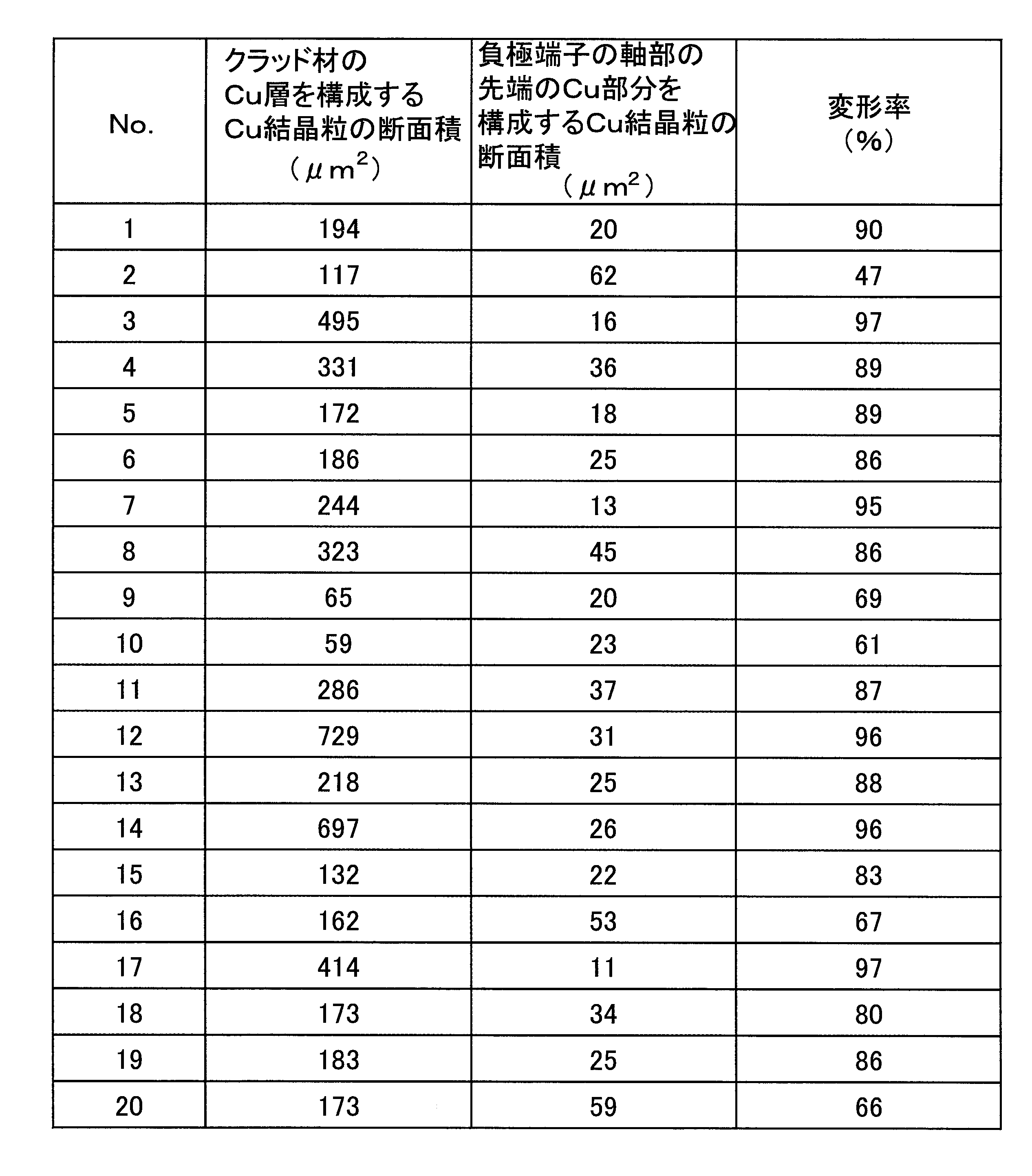
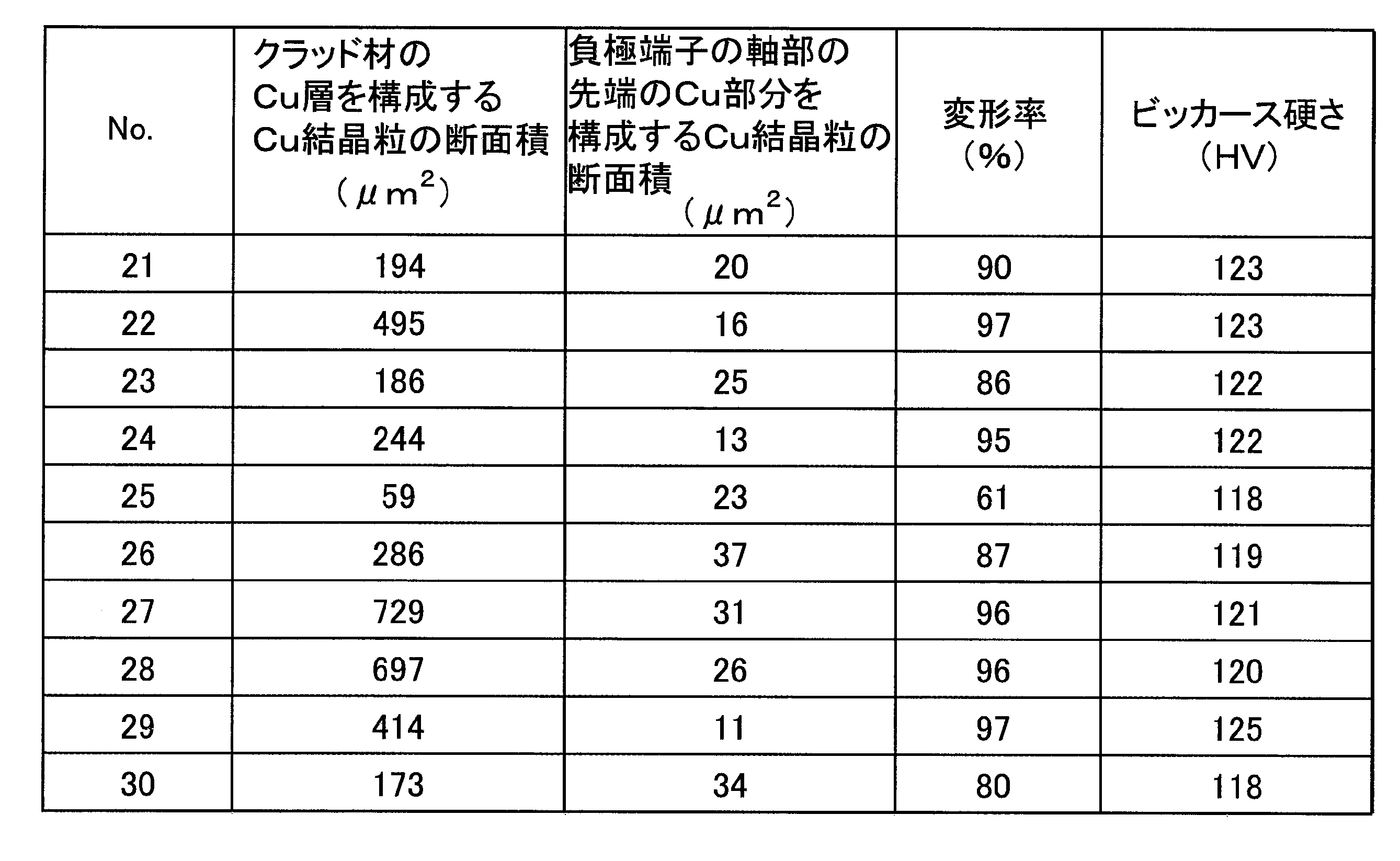
表1に示すように、No.1の場合、プレス加工前のクラッド材300におけるCu材320のCu結晶粒の断面積は、約194μm2であった。また、プレス加工後の負極端子20におけるCu部分33を構成するCu結晶粒の断面積は、約20μm2となった。そして、プレス加工前後のCu結晶粒の断面積の変形率Dは、約90%となった。
No.2の場合、プレス加工前のクラッド材300におけるCu材320を構成するCu結晶粒の断面積は、約117μm2であった。また、プレス加工後の負極端子20におけるCu部分33を構成するCu結晶粒の断面積は、約62μm2となった。そして、プレス加工前後のCu結晶粒の断面積の変形率Dは、約47%となった。
No.3の場合、プレス加工前のクラッド材300におけるCu材320のCu結晶粒の断面積は、約495μm2であった。また、プレス加工後の負極端子20におけるCu部分33のCu結晶粒の断面積は、約16μm2となった。そして、プレス加工前後のCu結晶粒の断面積の変形率Dは、約97%となった。
No.4の場合、プレス加工前のクラッド材300におけるCu材320のCu結晶粒の断面積は、約331μm2であった。また、プレス加工後の負極端子20におけるCu部分33を構成するCu結晶粒の断面積は、約36μm2となった。そして、プレス加工前後のCu結晶粒の断面積の変形率Dは、約89%となった。
No.5の場合、プレス加工前のクラッド材300におけるCu材320を構成するCu結晶粒の断面積は、約172μm2であった。また、プレス加工後の負極端子20におけるCu部分33を構成するCu結晶粒の断面積は、約18μm2となった。そして、プレス加工前後のCu結晶粒の断面積の変形率Dは、約89%となった。
No.6の場合、プレス加工前のクラッド材300におけるCu材320を構成するCu結晶粒の断面積は、約186μm2であった。また、プレス加工後の負極端子20におけるCu部分33を構成するCu結晶粒の断面積は、約25μm2となった。そして、プレス加工前後のCu結晶粒の断面積の変形率Dは、約86%となった。
No.7の場合、プレス加工前のクラッド材300におけるCu材320を構成するCu結晶粒の断面積は、約244μm2であった。また、プレス加工後の負極端子20におけるCu部分33を構成するCu結晶粒の断面積は、約13μm2となった。そして、プレス加工前後のCu結晶粒の断面積の変形率Dは、約95%となった。
No.8の場合、プレス加工前のクラッド材300におけるCu材320を構成するCu結晶粒の断面積は、約323μm2であった。また、プレス加工後の負極端子20におけるCu部分33を構成するCu結晶粒の断面積は、約45μm2となった。そして、プレス加工前後のCu結晶粒の断面積の変形率Dは、約86%となった。
No.9の場合、プレス加工前のクラッド材300におけるCu材320を構成するCu結晶粒の断面積は、約65μm2であった。また、プレス加工後の負極端子20におけるCu部分33を構成するCu結晶粒の断面積は、約20μm2となった。そして、プレス加工前後のCu結晶粒の断面積の変形率Dは、約69%となった。
No.10の場合、プレス加工前のクラッド材300におけるCu材320を構成するCu結晶粒の断面積は、約59μm2であった。また、プレス加工後の負極端子20におけるCu部分33を構成するCu結晶粒の断面積は、約23μm2となった。そして、プレス加工前後のCu結晶粒の断面積の変形率Dは、約61%となった。
No.11の場合、プレス加工前のクラッド材300におけるCu材320を構成するCu結晶粒の断面積は、約286μm2であった。また、プレス加工後の負極端子20におけるCu部分33を構成するCu結晶粒の断面積は、約37μm2となった。そして、プレス加工前後のCu結晶粒の断面積の変形率Dは、約87%となった。
No.12の場合、プレス加工前のクラッド材300におけるCu材320を構成するCu結晶粒の断面積は、約729μm2であった。また、プレス加工後の負極端子20におけるCu部分33を構成するCu結晶粒の断面積は、約31μm2となった。そして、プレス加工前後のCu結晶粒の断面積の変形率Dは、約96%となった。
No.13の場合、プレス加工前のクラッド材300におけるCu材320を構成するCu結晶粒の断面積は、約218μm2であった。また、プレス加工後の負極端子20におけるCu部分33を構成するCu結晶粒の断面積は、約25μm2となった。そして、プレス加工前後のCu結晶粒の断面積の変形率Dは、約88%となった。
No.14の場合、プレス加工前のクラッド材300におけるCu材320のCu結晶粒の断面積は、約697μm2であった。また、プレス加工後の負極端子20におけるCu部分33を構成するCu結晶粒の断面積は、約26μm2となった。そして、プレス加工前後のCu結晶粒の断面積の変形率Dは、約96%となった。
No.15の場合、プレス加工前のクラッド材300におけるCu材320のCu結晶粒の断面積は、約132μm2であった。また、プレス加工後の負極端子20におけるCu部分33を構成するCu結晶粒の断面積は、約22μm2となった。そして、プレス加工前後のCu結晶粒の断面積の変形率Dは、約83%となった。
No.16の場合、プレス加工前のクラッド材300におけるCu材320を構成するCu結晶粒の断面積は、約162μm2であった。また、プレス加工後の負極端子20におけるCu部分33を構成するCu結晶粒の断面積は、約53μm2となった。そして、プレス加工前後のCu結晶粒の断面積の変形率Dは、約67%となった。
No.17の場合、プレス加工前のクラッド材300におけるCu材320を構成するCu結晶粒の断面積は、約414μm2であった。また、プレス加工後の負極端子20におけるCu部分33を構成するCu結晶粒の断面積は、最も小さい約11μm2となった。そして、プレス加工前後のCu結晶粒の断面積の変形率Dは、約97%となった。
No.18の場合、プレス加工前のクラッド材300におけるCu材320を構成するCu結晶粒の断面積は、約173μm2であった。また、プレス加工後の負極端子20におけるCu部分33を構成するCu結晶粒の断面積は、約34μm2となった。そして、プレス加工前後のCu結晶粒の断面積の変形率Dは、約80%となった。
No.19の場合、プレス加工前のクラッド材300におけるCu材320を構成するCu結晶粒の断面積は、約183μm2であった。また、プレス加工後の負極端子20におけるCu部分33を構成するCu結晶粒の断面積は、約25μm2となった。そして、プレス加工前後のCu結晶粒の断面積の変形率Dは、約86%となった。
No.20の場合、プレス加工前のクラッド材300におけるCu材320を構成するCu結晶粒の断面積は、約173μm2であった。また、プレス加工後の負極端子20におけるCu部分33を構成するCu結晶粒の断面積は、約59μm2となった。そして、プレス加工前後のCu結晶粒の断面積の変形率Dは、約66%となった。
また、表2に示すように、No.21およびNo.22の場合、プレス加工後の負極端子20におけるCu部分33のビッカース硬さは、いずれも、約123HVとなった。
No.23およびNo.24の場合、プレス加工後の負極端子20におけるCu部分33のビッカース硬さは、いずれも、約122HVとなった。
No.25、No.26、No.27、No.28、No.29およびNo.30の場合、プレス加工後の負極端子20におけるCu部分33のビッカース硬さは、それぞれ順に、約118HV、約119HV、約121HV、約120HV、約125HVおよび約118HVとなった。
[実施例2]
上記実施例1の場合と同様に、実施例2(No.31~No.60)のクラッド材300を作製した。そして、作製したクラッド材300を用いて、上記実施例1の場合と同様に、実施例2(No.31~No.60)の負極端子20を作製した。なお、クラッド材300のプレス加工は、上記実施例1の場合と同様に、負極端子20の壁部24のCu層32からなるCu部分33を構成するCu結晶粒の断面積が10μm2以上100μm2以下、好ましくは10μm2以上65μm2以下、より好ましくは10μm2以上40μm2以下の範囲に収まるように、調整した。その結果、表3に示すように、負極端子20の壁部24のCu部分33のCu結晶粒の断面積は、10μm2以上100μm2以下の適切な範囲に収まった。なお、実施例2は、実施例1と異なるクラッド材300を用いて、実施例1と異なる負極端子20を作製した。実施例2のクラッド材300は、実施例1に対して、全体の体積比が約2.5倍で、Cu材320の体積比が約2.5倍である。また、実施例2の負極端子20は、実施例1に対して、軸部21の鍔部22よりもZ2側の部分(図7にt1で示す部分)の体積比が約4.5倍で、それ以外の部分の体積比が約3倍で、壁部24の体積比が約6倍で、壁部24の厚さ(肉厚)が約3倍である。
上記実施例1の場合と同様に、実施例2(No.31~No.60)のクラッド材300を作製した。そして、作製したクラッド材300を用いて、上記実施例1の場合と同様に、実施例2(No.31~No.60)の負極端子20を作製した。なお、クラッド材300のプレス加工は、上記実施例1の場合と同様に、負極端子20の壁部24のCu層32からなるCu部分33を構成するCu結晶粒の断面積が10μm2以上100μm2以下、好ましくは10μm2以上65μm2以下、より好ましくは10μm2以上40μm2以下の範囲に収まるように、調整した。その結果、表3に示すように、負極端子20の壁部24のCu部分33のCu結晶粒の断面積は、10μm2以上100μm2以下の適切な範囲に収まった。なお、実施例2は、実施例1と異なるクラッド材300を用いて、実施例1と異なる負極端子20を作製した。実施例2のクラッド材300は、実施例1に対して、全体の体積比が約2.5倍で、Cu材320の体積比が約2.5倍である。また、実施例2の負極端子20は、実施例1に対して、軸部21の鍔部22よりもZ2側の部分(図7にt1で示す部分)の体積比が約4.5倍で、それ以外の部分の体積比が約3倍で、壁部24の体積比が約6倍で、壁部24の厚さ(肉厚)が約3倍である。
作製したクラッド材300は、上記実施例1の場合と同様に、クラッド材300の厚み方向(Z方向)の切断面において、Cu材320を構成するCu結晶粒の断面積を測定した。測定結果を表3に示す。
そして、作製したクラッド材300から任意に選択した複数のクラッド材300の厚み方向(Z方向)の切断面において、上記実施例1の場合と同様に、Cu材320のビッカース硬さを測定したところ、たとえば、63HV、64HV、68HVなどとなり、その範囲は63HV以上68HV以下であり、その平均値は65.0HVであった。
作製した負極端子20は、上記実施例1の場合と同様に、負極端子20の軸部21の軸方向(Z方向)の切断面において、Cu部分33(Cu部分33a)を構成するCu結晶粒の断面積を測定した。測定結果を表3に示す。
そして、No.31~No.60の負極端子20から任意に選択してNo61~No.70とし、そのNo.61~No.70の負極端子20の軸部21の軸方向(Z方向)の切断面において、Cu材320のビッカース硬さを測定した。測定結果を表4に示す。
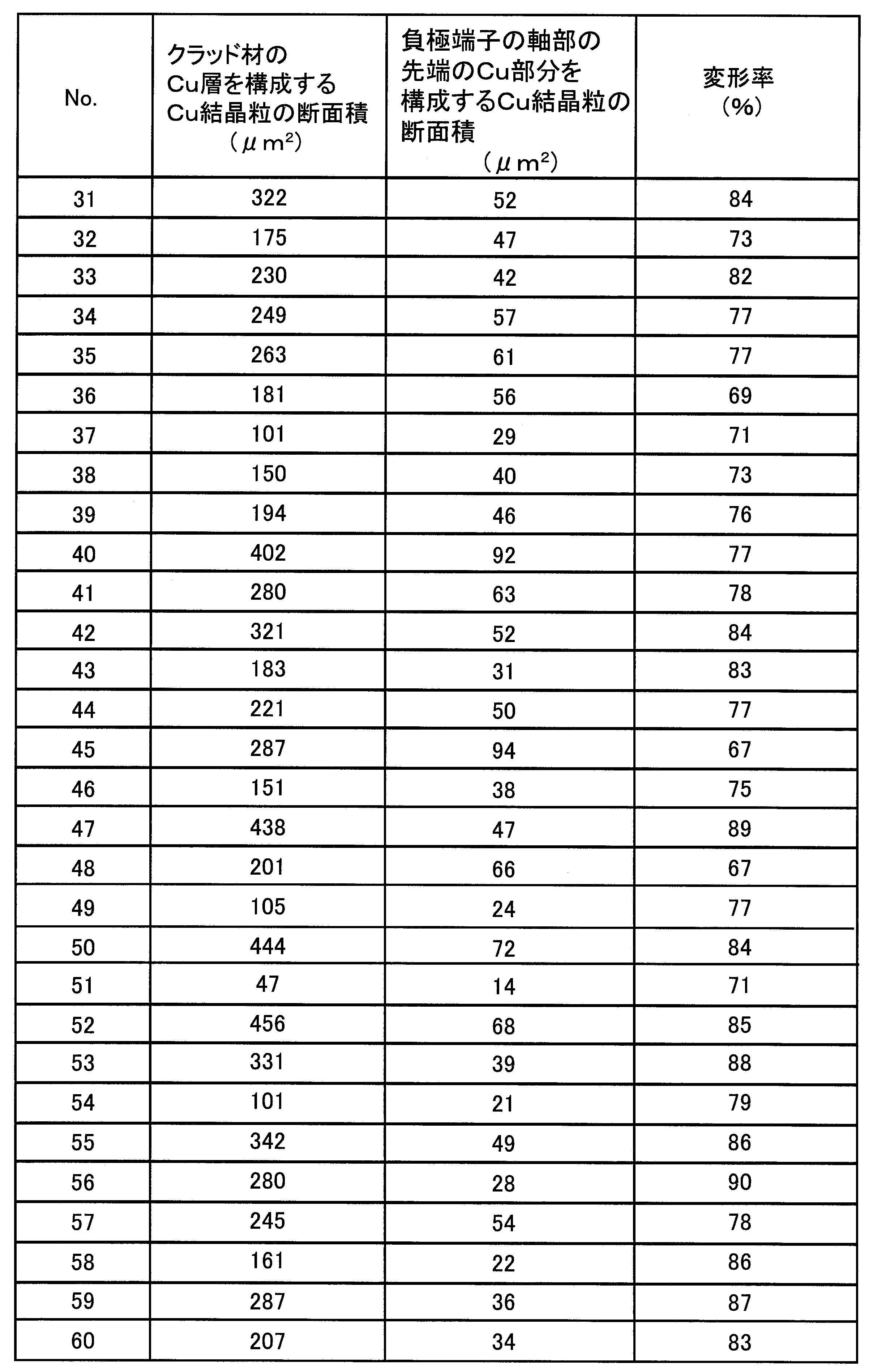
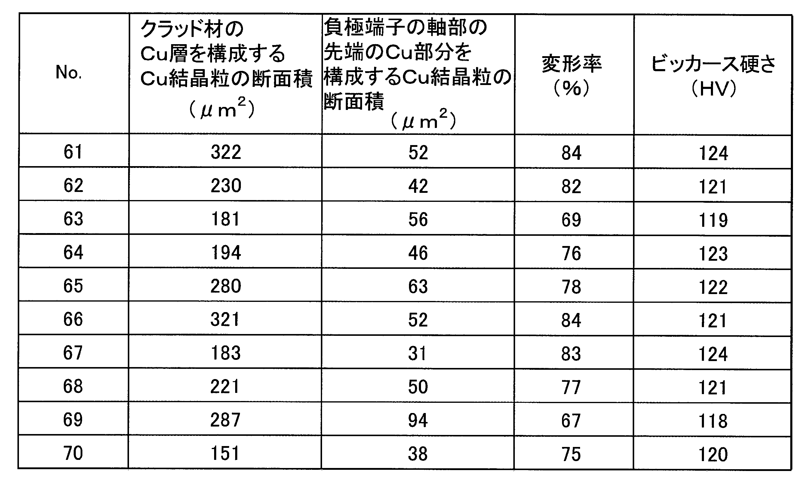
表3に示すように、No.31の場合、プレス加工前のクラッド材300におけるCu材320のCu結晶粒の断面積は、約322μm2であった。また、プレス加工後の負極端子20におけるCu部分33を構成するCu結晶粒の断面積は、約52μm2となった。そして、プレス加工前後のCu結晶粒の断面積の変形率Dは、約84%となった。
No.32の場合、プレス加工前のクラッド材300におけるCu材320のCu結晶粒の断面積は、約175μm2であった。また、プレス加工後の負極端子20におけるCu部分33を構成するCu結晶粒の断面積は、約47μm2となった。そして、プレス加工前後のCu結晶粒の断面積の変形率Dは、約73%となった。
No.33の場合、プレス加工前のクラッド材300におけるCu材320のCu結晶粒の断面積は、約230μm2であった。また、プレス加工後の負極端子20におけるCu部分33を構成するCu結晶粒の断面積は、約42μm2となった。そして、プレス加工前後のCu結晶粒の断面積の変形率Dは、約82%となった。
No.34の場合、プレス加工前のクラッド材300におけるCu材320のCu結晶粒の断面積は、約249μm2であった。また、プレス加工後の負極端子20におけるCu部分33を構成するCu結晶粒の断面積は、約57μm2となった。そして、プレス加工前後のCu結晶粒の断面積の変形率Dは、約77%となった。
No.35の場合、プレス加工前のクラッド材300におけるCu材320のCu結晶粒の断面積は、約263μm2であった。また、プレス加工後の負極端子20におけるCu部分33を構成するCu結晶粒の断面積は、約61μm2となった。そして、プレス加工前後のCu結晶粒の断面積の変形率Dは、約77%となった。
No.36の場合、プレス加工前のクラッド材300におけるCu材320のCu結晶粒の断面積は、約181μm2であった。また、プレス加工後の負極端子20におけるCu部分33を構成するCu結晶粒の断面積は、約56μm2となった。そして、プレス加工前後のCu結晶粒の断面積の変形率Dは、約69%となった。
No.37の場合、プレス加工前のクラッド材300におけるCu材320のCu結晶粒の断面積は、約101μm2であった。また、プレス加工後の負極端子20におけるCu部分33を構成するCu結晶粒の断面積は、約29μm2となった。そして、プレス加工前後のCu結晶粒の断面積の変形率Dは、約71%となった。
No.38の場合、プレス加工前のクラッド材300におけるCu材320のCu結晶粒の断面積は、約150μm2であった。また、プレス加工後の負極端子20におけるCu部分33を構成するCu結晶粒の断面積は、約40μm2となった。そして、プレス加工前後のCu結晶粒の断面積の変形率Dは、約73%となった。
No.39の場合、プレス加工前のクラッド材300におけるCu材320のCu結晶粒の断面積は、約194μm2であった。また、プレス加工後の負極端子20におけるCu部分33を構成するCu結晶粒の断面積は、約46μm2となった。そして、プレス加工前後のCu結晶粒の断面積の変形率Dは、約76%となった。
No.40の場合、プレス加工前のクラッド材300におけるCu材320のCu結晶粒の断面積は、約402μm2であった。また、プレス加工後の負極端子20におけるCu部分33を構成するCu結晶粒の断面積は、約92μm2となった。そして、プレス加工前後のCu結晶粒の断面積の変形率Dは、約77%となった。
No.41の場合、プレス加工前のクラッド材300におけるCu材320のCu結晶粒の断面積は、約280μm2であった。また、プレス加工後の負極端子20におけるCu部分33を構成するCu結晶粒の断面積は、約63μm2となった。そして、プレス加工前後のCu結晶粒の断面積の変形率Dは、約78%となった。
No.42の場合、プレス加工前のクラッド材300におけるCu材320のCu結晶粒の断面積は、約321μm2であった。また、プレス加工後の負極端子20におけるCu部分33を構成するCu結晶粒の断面積は、約52μm2となった。そして、プレス加工前後のCu結晶粒の断面積の変形率Dは、約84%となった。
No.43の場合、プレス加工前のクラッド材300におけるCu材320のCu結晶粒の断面積は、約183μm2であった。また、プレス加工後の負極端子20におけるCu部分33を構成するCu結晶粒の断面積は、約31μm2となった。そして、プレス加工前後のCu結晶粒の断面積の変形率Dは、約83%となった。
No.44の場合、プレス加工前のクラッド材300におけるCu材320のCu結晶粒の断面積は、約221μm2であった。また、プレス加工後の負極端子20におけるCu部分33を構成するCu結晶粒の断面積は、約50μm2となった。そして、プレス加工前後のCu結晶粒の断面積の変形率Dは、約77%となった。
No.45の場合、プレス加工前のクラッド材300におけるCu材320のCu結晶粒の断面積は、約287μm2であった。また、プレス加工後の負極端子20におけるCu部分33を構成するCu結晶粒の断面積は、約94μm2と一番大きくなった。そして、プレス加工前後のCu結晶粒の断面積の変形率Dは、約67%となった。
No.46の場合、プレス加工前のクラッド材300におけるCu材320のCu結晶粒の断面積は、約151μm2であった。また、プレス加工後の負極端子20におけるCu部分33を構成するCu結晶粒の断面積は、約38μm2となった。そして、プレス加工前後のCu結晶粒の断面積の変形率Dは、約75%となった。
No.47の場合、プレス加工前のクラッド材300におけるCu材320のCu結晶粒の断面積は、約438μm2であった。また、プレス加工後の負極端子20におけるCu部分33を構成するCu結晶粒の断面積は、約47μm2となった。そして、プレス加工前後のCu結晶粒の断面積の変形率Dは、約89%となった。
No.48の場合、プレス加工前のクラッド材300におけるCu材320のCu結晶粒の断面積は、約201μm2であった。また、プレス加工後の負極端子20におけるCu部分33を構成するCu結晶粒の断面積は、約66μm2となった。そして、プレス加工前後のCu結晶粒の断面積の変形率Dは、約67%となった。
No.49の場合、プレス加工前のクラッド材300におけるCu材320のCu結晶粒の断面積は、約105μm2であった。また、プレス加工後の負極端子20におけるCu部分33を構成するCu結晶粒の断面積は、約24μm2となった。そして、プレス加工前後のCu結晶粒の断面積の変形率Dは、約77%となった。
No.50の場合、プレス加工前のクラッド材300におけるCu材320のCu結晶粒の断面積は、約444μm2であった。また、プレス加工後の負極端子20におけるCu部分33を構成するCu結晶粒の断面積は、約72μm2となった。そして、プレス加工前後のCu結晶粒の断面積の変形率Dは、約84%となった。
No.51の場合、プレス加工前のクラッド材300におけるCu材320のCu結晶粒の断面積は、約47μm2であった。また、プレス加工後の負極端子20におけるCu部分33を構成するCu結晶粒の断面積は、約14μm2となった。そして、プレス加工前後のCu結晶粒の断面積の変形率Dは、約71%となった。
No.52の場合、プレス加工前のクラッド材300におけるCu材320のCu結晶粒の断面積は、約456μm2であった。また、プレス加工後の負極端子20におけるCu部分33を構成するCu結晶粒の断面積は、約68μm2となった。そして、プレス加工前後のCu結晶粒の断面積の変形率Dは、約85%となった。
No.53の場合、プレス加工前のクラッド材300におけるCu材320のCu結晶粒の断面積は、約331μm2であった。また、プレス加工後の負極端子20におけるCu部分33を構成するCu結晶粒の断面積は、約39μm2となった。そして、プレス加工前後のCu結晶粒の断面積の変形率Dは、約88%となった。
No.54の場合、プレス加工前のクラッド材300におけるCu材320のCu結晶粒の断面積は、約101μm2であった。また、プレス加工後の負極端子20におけるCu部分33を構成するCu結晶粒の断面積は、約21μm2となった。そして、プレス加工前後のCu結晶粒の断面積の変形率Dは、約79%となった。
No.55の場合、プレス加工前のクラッド材300におけるCu材320のCu結晶粒の断面積は、約342μm2であった。また、プレス加工後の負極端子20におけるCu部分33を構成するCu結晶粒の断面積は、約49μm2となった。そして、プレス加工前後のCu結晶粒の断面積の変形率Dは、約86%となった。
No.56の場合、プレス加工前のクラッド材300におけるCu材320のCu結晶粒の断面積は、約280μm2であった。また、プレス加工後の負極端子20におけるCu部分33を構成するCu結晶粒の断面積は、約28μm2となった。そして、プレス加工前後のCu結晶粒の断面積の変形率Dは、約90%となった。
No.57の場合、プレス加工前のクラッド材300におけるCu材320のCu結晶粒の断面積は、約245μm2であった。また、プレス加工後の負極端子20におけるCu部分33を構成するCu結晶粒の断面積は、約54μm2となった。そして、プレス加工前後のCu結晶粒の断面積の変形率Dは、約78%となった。
No.58の場合、プレス加工前のクラッド材300におけるCu材320のCu結晶粒の断面積は、約161μm2であった。また、プレス加工後の負極端子20におけるCu部分33を構成するCu結晶粒の断面積は、約22μm2となった。そして、プレス加工前後のCu結晶粒の断面積の変形率Dは、約86%となった。
No.59の場合、プレス加工前のクラッド材300におけるCu材320のCu結晶粒の断面積は、約287μm2であった。また、プレス加工後の負極端子20におけるCu部分33を構成するCu結晶粒の断面積は、約36μm2となった。そして、プレス加工前後のCu結晶粒の断面積の変形率Dは、約87%となった。
No.60の場合、プレス加工前のクラッド材300におけるCu材320のCu結晶粒の断面積は、約207μm2であった。また、プレス加工後の負極端子20におけるCu部分33を構成するCu結晶粒の断面積は、約34μm2となった。そして、プレス加工前後のCu結晶粒の断面積の変形率Dは、約83%となった。
また、表4に示すように、No.61およびNo.67の場合、プレス加工後の負極端子20におけるCu部分33のビッカース硬さは、いずれも、約124HVとなった。
No.62、No.66およびNo.68の場合、プレス加工後の負極端子20におけるCu部分33のビッカース硬さは、いずれも、約121HVとなった。
No.63、No.64、No.65、No.69およびNo.70の場合、プレス加工後の負極端子20におけるCu部分33のビッカース硬さは、それぞれ順に、約119HV、約123HV、約122HV、約118HVおよび約120HVとなった。
上記実施例1および上記実施例2のクラッド材300(No.1~20およびNo.31~60)をプレス加工して負極端子20を作製した際に、負極端子20の壁部24のCu層32からなるCu部分33を構成するCu結晶粒の断面積を確認した。そして、実施例1の負極端子20(No.1~20)の壁部24のCu部分33を構成するCu結晶粒の断面積が、10μm2以上65μm2以下のより適切な範囲になっていることを確認することができた。また、実施例2の負極端子20(No.31~No.60)の壁部24のCu部分33を構成するCu結晶粒の断面積が、10μm2以上100μm2以下の適切な範囲になっていることを確認することができた。さらに、実施例1および実施例2の負極端子20(No.1~No.20およびNo.31~No.60)の特に壁部24において、割れが生じていないことを確認することができた。特に、No.40のクラッド材は、Cu結晶粒の断面積が94μm2であり、実施例の中で最も結晶粒が最大となるとともに、ビッカース硬さが118HVと十分な加工性を有する硬さとなり、十分な機械的強度を有していた。また、No.41のクラッド材は、Cu結晶粒の断面積が63μm2であり、ビッカース硬さが122HVであるため、さらに加工性が向上し、十分な機械的強度を有していた。また、No.29クラッド材は、Cu結晶粒の断面積が11μm2と実施例の中で一番断面積が小さいが、ビッカース硬さが125HVと最も大きく、十分な加工性を有するとともに最適な機械的強度を有していた。
実施例1および実施例2の結果から、本願発明者は、負極端子20の壁部24のCu層32からなるCu部分33を構成するCu結晶粒の断面積が10μm2以上100μm2以下に収まるように、クラッド材300をプレス加工することにより、図10に示すようなクラッド材300から図6に示すような負極端子20を割れなく作製することができることを見出した。
また、本願発明者は、実施例1および実施例2の結果から得られた結果と、製造時に生じうるビッカース硬さの誤差(ばらつき)とを考慮した結果とから、Cu部分33を構成するCu結晶粒の断面積が10μm2以上100μm2以下に収まるようにクラッド材300をプレス加工することにより、ビッカース硬さを110HV以上125HV以下にすることが可能であることを見出した。また、本願発明者は、実施例1および実施例2の結果から得られた結果と、製造時に生じうるビッカース硬さの誤差(ばらつき)とを考慮した結果から、Cu部分33を構成するCu結晶粒の断面積が10μm2以上65μm2以下に収まるように、クラッド材300をプレス加工することにより、ビッカース硬さを115HV以上125HV以下にすることが可能であることを見出した。そして、本願発明者は、Cu部分33を構成するCu結晶粒の断面積を10μm2以上40μm2以下に調整することにより、ビッカース硬さが118HV以上125HV以下にすることが可能であることを見出した。
また、本願発明者は、No.67の結果とNo.69の結果とから、Cu部分33を構成するCu結晶粒の断面積の差が約60μm2の場合でも、ビッカース硬さの差を6HVの範囲に収まることを知得した。また、この結果から、本願発明者は、Cu結晶粒の断面積をNo.69の94μm2から100μm2に大きくした場合に、ビッカース硬さが110HV未満にならないことを見出した。そして、図10に示すようなクラッド材300を用いて、壁部24のCu層32からなるCu部分33を構成するCu結晶粒の断面積が10μm2以上100μm2以下となるようにプレス加工して作製された負極端子20は、ビッカース硬さが110HV以上125HV以下である適度な硬さのCu部分33を有することができることを見出した。
また、本願発明者は、壁部24のCu層32からなるCu部分33を構成するCu結晶粒の断面積が10μm2以上100μm2以下となる負極端子20は、図10に示すようなクラッド材300を用いて、クラッド材300のCu材320を構成するCu結晶粒(断面積S1)をCu結晶粒の断面積の変形率Dが45%以上100%未満となるようにプレス加工することにより作製することができることを見出した。
また、本願発明者は、壁部24のCu層32からなるCu部分33を構成するCu結晶粒の断面積が10μm2以上100μm2以下となる負極端子20は、Cu材320のビッカース硬さが70HV以下である図10に示すようなクラッド材300を用いて、45%以上100%未満の変形率Dで、壁部24のCu層32からなるCu部分33のビッカース硬さが110HV以上125HV以下となるようにプレス加工することにより作製することができることを見出した。
次に、実施例1および実施例2の作製した負極端子20(No.1~No.20およびNo.31~No.60)を用いて、本実施形態と同様に図15から図18に示すような壁部24の折り曲げ、かしめ、レーザ溶接を行って固定状態(かしめ状態)とした。その際に、負極端子20(特に壁部24の基部領域27)に割れが生じていないことを確認することができた。この結果から、本願発明者は、図10に示すようなクラッド材300を用いて、壁部24のCu層32からなるCu部分33を構成するCu結晶粒の断面積が10μm2以上100μm2以下となるようにプレス加工して作製された負極端子20は、軸部21の先端のCu部分33が適切な断面積を有するCu結晶粒により構成されているため、軸部21の先端のCu部分33を折り曲げてかしめることにより他の部材に固定するのに好適な機械的特性を有することができることを見出した。
次に、実施例1および実施例2の負極端子20(No.1~No.20およびNo.31~No.60)を上記固定状態(かしめ状態)とした後に、車載用途を想定して適度な振動を与え続けた。その際に、負極端子20(特に壁部24の基部領域27)に割れが生じていないことを確認することができた。この結果から、本願発明者は、図10に示すようなクラッド材300を用いて、壁部24のCu層32からなるCu部分33を構成するCu結晶粒の断面積が10μm2以上100μm2以下となるようにプレス加工して作製された負極端子20は、軸部21の先端のCu部分33が適切な断面積を有するCu結晶粒により構成されているため、軸部21の先端のCu部分33を折り曲げてかしめた固定状態(かしめ状態)に経時的に耐えて維持するために適切な機械的特性を有することができることを見出した。
[変形例]
なお、今回開示された実施形態および実施例は、すべての点で例示であって制限的なものではないと考えられるべきである。本発明の範囲は、上記した実施形態および実施例の説明ではなく請求の範囲によって示され、さらに請求の範囲と均等の意味および範囲内でのすべての変更(変形例)が含まれる。
なお、今回開示された実施形態および実施例は、すべての点で例示であって制限的なものではないと考えられるべきである。本発明の範囲は、上記した実施形態および実施例の説明ではなく請求の範囲によって示され、さらに請求の範囲と均等の意味および範囲内でのすべての変更(変形例)が含まれる。
たとえば、本実施形態では、Al層とCu層とが積層されて接合された2層構造のクラッド材の例を示したが、本発明はこれに限られない。本発明では、たとえば、Al層とCu層とNi層とがこの順で積層されて接合された3層構造のクラッド材であってもよい。
また、本実施形態では、Al層とCu層とが積層されて接合された2層構造のクラッド材の例を示したが、本発明はこれに限られない。本発明では、3層構造以上であってもよい。その場合、たとえば、4層構造のクラッド材であってもよく、Al層とNi層とCu層とNi層とがこの順で積層されて接合された4層構造のクラッド材であってもよい。また、3層構造以上の場合、Cu層からなるCu部分の結晶粒の断面積が、10μm2以上100μm2以下であれば、クラッド材は、十分な機械的強度を有する。
また、本実施形態では、電池用端子である負極端子20の壁部24のCu部分33が折り曲げられる例を示したが、本発明はこれに限られない。本発明では、たとえば、図19に示すように壁部のCu部分がフレア加工される電池用端子であってもよい。
また、本実施形態では、ビッカース硬さなどを壁部24の基部領域27のCu部分33(Cu部分33a)において測定する例を示したが、本発明はこれに限られない。本発明では、たとえば、ビッカース硬さなどを壁部24のCu部分33のZ2側の先端部において測定してもよい。
また、本実施形態では、凹部23は、Z2側から見て、丸パイプ断面のような円環状に形成されている例を示したが、本発明はこれに限られない。本発明では、凹部は、Z2方向から見て円環状でなくてもよく、たとえば、矩形状であってもよい。
また、本実施形態では、鍔部12が、Z方向から見て円環状である例を示したが、本発明はこれに限られない。本発明では、鍔部は、Z方向から見て円環状でなくてもよく、たとえば、矩形状であってもよい。
また、本実施形態では、電池用端子を組電池100の負極端子20として用いた例を示したが、本発明はこれに限られない。本発明では、電池用端子を単電池の負極端子として用いてもよい。
20 負極端子(電池用端子)
21 軸部
22 鍔部
23 凹部
24 壁部
27 基部領域
31 Al層
32 Cu層
33 Cu部分
130 クラッド材(帯状のクラッド材)
131 Al板材
132 Cu板材
300 クラッド材(個片状のクラッド材)
310 Al材
320 Cu材
21 軸部
22 鍔部
23 凹部
24 壁部
27 基部領域
31 Al層
32 Cu層
33 Cu部分
130 クラッド材(帯状のクラッド材)
131 Al板材
132 Cu板材
300 クラッド材(個片状のクラッド材)
310 Al材
320 Cu材
Claims (11)
- 純AlまたはAl基合金から構成されるAl層(31)と、
純CuまたはCu基合金から構成されるCu層(32)とが、この順に積層された状態で接合されたクラッド材から構成され、
前記Al層側から前記Cu層側に延びる軸部(21)と、前記軸部の側方から放射方向に広がる鍔部(22)と、前記軸部の前記Cu層側の先端からさらに延びる壁部に囲まれる凹部(23)と、を備え、
前記軸部の軸方向の切断面において、前記壁部の前記Cu層からなるCu部分を構成するCu結晶粒の断面積は、10μm2以上100μm2以下である、電池用端子。 - 前記Cu部分を構成するCu結晶粒の断面積は、65μm2以下である、請求項1に記載の電池用端子。
- 前記Cu部分を構成するCu結晶粒の断面積は、40μm2以下である、請求項2に記載の電池用端子。
- 前記Cu部分のビッカース硬さは、110HV以上125HV以下である、請求項1~3のいずれか1項に記載の電池用端子。
- 純AlまたはAl基合金からなるAl板材(131)と、純CuまたはCu基合金からなるCu板材(132)とを、この順に積層した状態で接合することによって、Al材(310)およびCu材(320)により構成されたクラッド材(300)を形成する工程と、
前記クラッド材をプレス加工することによって、クラッド材のAl材からなるAl層(31)と、クラッド材のCu材からなるCu層(32)とが、この順に積層された状態で接合され、前記Al層側から前記Cu層側に延びる軸部(21)と、前記軸部の側方から放射方向に広がる鍔部(22)と、前記軸部の前記Cu層側の先端からさらに延びる壁部に囲まれる凹部(23)とを含む、電池用端子を形成する工程と、を備え、
前記電池用端子を形成する工程は、前記軸部の軸方向の切断面において、前記壁部の前記Cu層からなるCu部分を構成するCu結晶粒の断面積が10μm2以上100μm2以下になるように、前記クラッド材をプレス加工する工程を含む、電池用端子の製造方法。 - 前記電池用端子を形成する工程は、前記Cu部分を構成するCu結晶粒の断面積が65μm2以下になるように、前記クラッド材をプレス加工する工程を含む、請求項5に記載の電池用端子の製造方法。
- 前記電池用端子を形成する工程は、前記Cu部分を構成するCu結晶粒の断面積が40μm2以下になるように、前記クラッド材をプレス加工する工程を含む、請求項6に記載の電池用端子の製造方法。
- 前記電池用端子を形成する工程は、前記クラッド材の厚み方向の切断面において、前記Cu材を構成するCu結晶粒の断面積をS1とし、前記軸部の軸方向の切断面において、前記Cu部分を構成するCu結晶粒の断面積をS2とするとき、(S1-S2)/S1×100で求まるプレス加工前後のCu結晶粒の変形率が45%以上100%未満になるように、前記凹部を形成する工程を含む、請求項5~7のいずれか1項に記載の電池用端子の製造方法。
- 前記電池用端子を形成する工程は、前記変形率が60%以上になるように、前記凹部を形成する工程を含む、請求項8に記載の電池用端子の製造方法。
- 前記クラッド材を形成する工程は、前記クラッド材の厚み方向の切断面において、前記Cu材のビッカース硬さが70HV以下になるように、前記クラッド材を形成する工程を含む、請求項5~9のいずれか1項に記載の電池用端子の製造方法。
- 前記電池用端子を形成する工程は、前記Cu部分のビッカース硬さが110HV以上125HV以下になるように、前記クラッド材をプレス加工する工程を含む、請求項5~10のいずれか1項に記載の電池用端子の製造方法。
Priority Applications (1)
| Application Number | Priority Date | Filing Date | Title |
|---|---|---|---|
| JP2022511526A JP7336025B2 (ja) | 2020-03-31 | 2020-12-17 | 電池用端子および電池用端子の製造方法 |
Applications Claiming Priority (2)
| Application Number | Priority Date | Filing Date | Title |
|---|---|---|---|
| JP2020-063253 | 2020-03-31 | ||
| JP2020063253 | 2020-03-31 |
Publications (1)
| Publication Number | Publication Date |
|---|---|
| WO2021199518A1 true WO2021199518A1 (ja) | 2021-10-07 |
Family
ID=77344695
Family Applications (1)
| Application Number | Title | Priority Date | Filing Date |
|---|---|---|---|
| PCT/JP2020/047232 Ceased WO2021199518A1 (ja) | 2020-03-31 | 2020-12-17 | 電池用端子および電池用端子の製造方法 |
Country Status (3)
| Country | Link |
|---|---|
| JP (1) | JP7336025B2 (ja) |
| CN (1) | CN214043930U (ja) |
| WO (1) | WO2021199518A1 (ja) |
Cited By (6)
| Publication number | Priority date | Publication date | Assignee | Title |
|---|---|---|---|---|
| JP2023062844A (ja) * | 2021-10-22 | 2023-05-09 | プライムプラネットエナジー&ソリューションズ株式会社 | 端子部品、二次電池、および、端子部品の製造方法 |
| JP2024007719A (ja) * | 2022-07-06 | 2024-01-19 | プライムアースEvエナジー株式会社 | リベットおよびリベットを用いた電池 |
| JPWO2024135642A1 (ja) * | 2022-12-20 | 2024-06-27 | ||
| WO2025126564A1 (ja) * | 2023-12-11 | 2025-06-19 | 株式会社プロテリアル | 電池用端子部品の製造方法 |
| WO2025126565A1 (ja) * | 2023-12-11 | 2025-06-19 | 株式会社プロテリアル | 電池用端子部品の製造方法 |
| WO2026083620A1 (ja) * | 2024-10-15 | 2026-04-23 | ビークルエナジージャパン株式会社 | 電池及び組電池 |
Families Citing this family (1)
| Publication number | Priority date | Publication date | Assignee | Title |
|---|---|---|---|---|
| CN117884533A (zh) * | 2024-03-15 | 2024-04-16 | 蜂巢能源科技股份有限公司 | 盖板装配成型工艺及盖板 |
Citations (4)
| Publication number | Priority date | Publication date | Assignee | Title |
|---|---|---|---|---|
| JPH08162088A (ja) * | 1994-11-30 | 1996-06-21 | Sanyo Electric Co Ltd | 円筒型非水電解液電池 |
| JP2004063133A (ja) * | 2002-07-25 | 2004-02-26 | Toshiba Corp | 薄型二次電池 |
| JP2004106059A (ja) * | 2002-08-29 | 2004-04-08 | Sumitomo Special Metals Co Ltd | アルミニウム/ニッケルクラッド材およびその製造方法並びに電池用外部端子 |
| JP6014808B1 (ja) * | 2015-08-17 | 2016-10-26 | 日立金属株式会社 | 電池用端子および電池用端子の製造方法 |
Family Cites Families (3)
| Publication number | Priority date | Publication date | Assignee | Title |
|---|---|---|---|---|
| JP3681327B2 (ja) * | 2000-09-19 | 2005-08-10 | 福井鋲螺株式会社 | 極薄積層体の導通方法及びシート状電極 |
| US6854634B2 (en) * | 2002-05-14 | 2005-02-15 | The Boeing Company | Method of manufacturing rivets having high strength and formability |
| JP4880336B2 (ja) * | 2006-03-20 | 2012-02-22 | 日産自動車株式会社 | セルフピアスリベットおよびその製造方法 |
-
2020
- 2020-12-17 JP JP2022511526A patent/JP7336025B2/ja active Active
- 2020-12-17 WO PCT/JP2020/047232 patent/WO2021199518A1/ja not_active Ceased
- 2020-12-30 CN CN202023296105.6U patent/CN214043930U/zh active Active
Patent Citations (4)
| Publication number | Priority date | Publication date | Assignee | Title |
|---|---|---|---|---|
| JPH08162088A (ja) * | 1994-11-30 | 1996-06-21 | Sanyo Electric Co Ltd | 円筒型非水電解液電池 |
| JP2004063133A (ja) * | 2002-07-25 | 2004-02-26 | Toshiba Corp | 薄型二次電池 |
| JP2004106059A (ja) * | 2002-08-29 | 2004-04-08 | Sumitomo Special Metals Co Ltd | アルミニウム/ニッケルクラッド材およびその製造方法並びに電池用外部端子 |
| JP6014808B1 (ja) * | 2015-08-17 | 2016-10-26 | 日立金属株式会社 | 電池用端子および電池用端子の製造方法 |
Cited By (9)
| Publication number | Priority date | Publication date | Assignee | Title |
|---|---|---|---|---|
| JP2023062844A (ja) * | 2021-10-22 | 2023-05-09 | プライムプラネットエナジー&ソリューションズ株式会社 | 端子部品、二次電池、および、端子部品の製造方法 |
| JP7405811B2 (ja) | 2021-10-22 | 2023-12-26 | プライムプラネットエナジー&ソリューションズ株式会社 | 端子部品、二次電池、および、端子部品の製造方法 |
| JP2024007719A (ja) * | 2022-07-06 | 2024-01-19 | プライムアースEvエナジー株式会社 | リベットおよびリベットを用いた電池 |
| JP7832857B2 (ja) | 2022-07-06 | 2026-03-18 | トヨタバッテリー株式会社 | リベットおよびリベットを用いた電池 |
| JPWO2024135642A1 (ja) * | 2022-12-20 | 2024-06-27 | ||
| JP7871902B2 (ja) | 2022-12-20 | 2026-06-09 | 株式会社プロテリアル | 電池用端子、電池用端子の製造方法、電池および電池の製造方法 |
| WO2025126564A1 (ja) * | 2023-12-11 | 2025-06-19 | 株式会社プロテリアル | 電池用端子部品の製造方法 |
| WO2025126565A1 (ja) * | 2023-12-11 | 2025-06-19 | 株式会社プロテリアル | 電池用端子部品の製造方法 |
| WO2026083620A1 (ja) * | 2024-10-15 | 2026-04-23 | ビークルエナジージャパン株式会社 | 電池及び組電池 |
Also Published As
| Publication number | Publication date |
|---|---|
| JPWO2021199518A1 (ja) | 2021-10-07 |
| CN214043930U (zh) | 2021-08-24 |
| JP7336025B2 (ja) | 2023-08-30 |
Similar Documents
| Publication | Publication Date | Title |
|---|---|---|
| JP7336025B2 (ja) | 電池用端子および電池用端子の製造方法 | |
| KR102819010B1 (ko) | 단자 부품, 그것을 구비한 이차 전지 및 조전지 그리고 단자 부품의 제조 방법 | |
| JP6592946B2 (ja) | 電池負極リード材用クラッド材および電池負極リード材用クラッド材の製造方法 | |
| US10026947B2 (en) | Battery terminal and method for manufacturing battery | |
| JP6970227B2 (ja) | クラッド端子、電池用端子およびクラッド端子の製造方法 | |
| US10193126B2 (en) | Battery terminal, method for manufacturing battery terminal, and battery | |
| JP5329290B2 (ja) | リチウムイオン電池の負極集電体用クラッド材及びその製造方法 | |
| CN106531946B (zh) | 电池用引线部件和电池用引线部件的制造方法 | |
| JP2000317531A (ja) | 板材のプレス加工方法 | |
| JP7124842B2 (ja) | 端子のシール構造 | |
| JP7405811B2 (ja) | 端子部品、二次電池、および、端子部品の製造方法 | |
| CN102138190A (zh) | 电子零件用端子的制造方法及通过该制造方法得到的电子零件用端子 | |
| JP4612483B2 (ja) | アルミニウム合金−チタン溝付き複合板の製造方法 | |
| JPWO2019107223A1 (ja) | 電池集電体用クラッド材および電池集電体用クラッド材の製造方法 | |
| JP2004351460A (ja) | アルミニウム・ニッケル・ステンレス鋼クラッド材、その製造方法および電池用ケース | |
| JP2006051523A (ja) | 導電部品用クラッド材およびその製造方法 | |
| KR20250168659A (ko) | 레이저 용접용 클래드재, 레이저 용접용 클래드재를 사용한 접합 구조 및 전지의 제조 방법 | |
| WO2024135642A1 (ja) | 電池用端子、電池用端子の製造方法、電池および電池の製造方法 | |
| JP4774297B2 (ja) | 鉛蓄電池用格子体の製造方法および鉛蓄電池 | |
| JP7172311B2 (ja) | 二次電池の負極集電体用箔およびその製造方法、二次電池の負極およびその製造方法 | |
| WO2024241839A1 (ja) | ワイヤボンディング用クラッド材、ワイヤボンディング用クラッド材を用いた接合構造、および電池の製造方法 | |
| JP2020047510A (ja) | 電池封口体用クラッド材およびその製造方法 | |
| JP2025187874A (ja) | クラッド構造体および電池用端子部品 | |
| KR20250110725A (ko) | 고강도 금속 캔 및 이에 수용된 이차전지 | |
| WO2024054692A1 (en) | Deep drawable clad systems and methods thereof |
Legal Events
| Date | Code | Title | Description |
|---|---|---|---|
| 121 | Ep: the epo has been informed by wipo that ep was designated in this application |
Ref document number: 20928405 Country of ref document: EP Kind code of ref document: A1 |
|
| ENP | Entry into the national phase |
Ref document number: 2022511526 Country of ref document: JP Kind code of ref document: A |
|
| NENP | Non-entry into the national phase |
Ref country code: DE |
|
| 122 | Ep: pct application non-entry in european phase |
Ref document number: 20928405 Country of ref document: EP Kind code of ref document: A1 |