WO2021193623A1 - 電子機器 - Google Patents
電子機器 Download PDFInfo
- Publication number
- WO2021193623A1 WO2021193623A1 PCT/JP2021/011969 JP2021011969W WO2021193623A1 WO 2021193623 A1 WO2021193623 A1 WO 2021193623A1 JP 2021011969 W JP2021011969 W JP 2021011969W WO 2021193623 A1 WO2021193623 A1 WO 2021193623A1
- Authority
- WO
- WIPO (PCT)
- Prior art keywords
- circuit board
- electronic device
- guided
- button
- movable portion
- Prior art date
- Legal status (The legal status is an assumption and is not a legal conclusion. Google has not performed a legal analysis and makes no representation as to the accuracy of the status listed.)
- Ceased
Links
Images


Classifications
-
- H—ELECTRICITY
- H01—ELECTRIC ELEMENTS
- H01H—ELECTRIC SWITCHES; RELAYS; SELECTORS; EMERGENCY PROTECTIVE DEVICES
- H01H13/00—Switches having rectilinearly-movable operating part or parts adapted for pushing or pulling in one direction only, e.g. push-button switch
- H01H13/02—Details
- H01H13/12—Movable parts; Contacts mounted thereon
- H01H13/14—Operating parts, e.g. push-button
-
- H—ELECTRICITY
- H01—ELECTRIC ELEMENTS
- H01H—ELECTRIC SWITCHES; RELAYS; SELECTORS; EMERGENCY PROTECTIVE DEVICES
- H01H13/00—Switches having rectilinearly-movable operating part or parts adapted for pushing or pulling in one direction only, e.g. push-button switch
- H01H13/70—Switches having rectilinearly-movable operating part or parts adapted for pushing or pulling in one direction only, e.g. push-button switch having a plurality of operating members associated with different sets of contacts, e.g. keyboard
- H01H13/702—Switches having rectilinearly-movable operating part or parts adapted for pushing or pulling in one direction only, e.g. push-button switch having a plurality of operating members associated with different sets of contacts, e.g. keyboard with contacts carried by or formed from layers in a multilayer structure, e.g. membrane switches
- H01H13/705—Switches having rectilinearly-movable operating part or parts adapted for pushing or pulling in one direction only, e.g. push-button switch having a plurality of operating members associated with different sets of contacts, e.g. keyboard with contacts carried by or formed from layers in a multilayer structure, e.g. membrane switches characterised by construction, mounting or arrangement of operating parts, e.g. push-buttons or keys
-
- H—ELECTRICITY
- H01—ELECTRIC ELEMENTS
- H01H—ELECTRIC SWITCHES; RELAYS; SELECTORS; EMERGENCY PROTECTIVE DEVICES
- H01H13/00—Switches having rectilinearly-movable operating part or parts adapted for pushing or pulling in one direction only, e.g. push-button switch
- H01H13/02—Details
- H01H13/12—Movable parts; Contacts mounted thereon
- H01H13/20—Driving mechanisms
-
- H—ELECTRICITY
- H05—ELECTRIC TECHNIQUES NOT OTHERWISE PROVIDED FOR
- H05K—PRINTED CIRCUITS; CASINGS OR CONSTRUCTIONAL DETAILS OF ELECTRIC APPARATUS; MANUFACTURE OF ASSEMBLAGES OF ELECTRICAL COMPONENTS
- H05K1/00—Printed circuits
- H05K1/18—Printed circuits structurally associated with non-printed electric components
- H05K1/181—Printed circuits structurally associated with non-printed electric components associated with surface mounted components
-
- H—ELECTRICITY
- H05—ELECTRIC TECHNIQUES NOT OTHERWISE PROVIDED FOR
- H05K—PRINTED CIRCUITS; CASINGS OR CONSTRUCTIONAL DETAILS OF ELECTRIC APPARATUS; MANUFACTURE OF ASSEMBLAGES OF ELECTRICAL COMPONENTS
- H05K7/00—Constructional details common to different types of electric apparatus
- H05K7/02—Arrangements of circuit components or wiring on supporting structure
- H05K7/12—Resilient or clamping means for holding component to structure
-
- H—ELECTRICITY
- H01—ELECTRIC ELEMENTS
- H01H—ELECTRIC SWITCHES; RELAYS; SELECTORS; EMERGENCY PROTECTIVE DEVICES
- H01H2221/00—Actuators
- H01H2221/024—Transmission element
- H01H2221/026—Guiding or lubricating nylon
-
- H—ELECTRICITY
- H01—ELECTRIC ELEMENTS
- H01H—ELECTRIC SWITCHES; RELAYS; SELECTORS; EMERGENCY PROTECTIVE DEVICES
- H01H2221/00—Actuators
- H01H2221/036—Return force
- H01H2221/044—Elastic part on actuator or casing
-
- H—ELECTRICITY
- H01—ELECTRIC ELEMENTS
- H01H—ELECTRIC SWITCHES; RELAYS; SELECTORS; EMERGENCY PROTECTIVE DEVICES
- H01H2221/00—Actuators
- H01H2221/058—Actuators to avoid tilting or skewing of contact area or actuator
-
- H—ELECTRICITY
- H05—ELECTRIC TECHNIQUES NOT OTHERWISE PROVIDED FOR
- H05K—PRINTED CIRCUITS; CASINGS OR CONSTRUCTIONAL DETAILS OF ELECTRIC APPARATUS; MANUFACTURE OF ASSEMBLAGES OF ELECTRICAL COMPONENTS
- H05K1/00—Printed circuits
- H05K1/18—Printed circuits structurally associated with non-printed electric components
-
- H—ELECTRICITY
- H05—ELECTRIC TECHNIQUES NOT OTHERWISE PROVIDED FOR
- H05K—PRINTED CIRCUITS; CASINGS OR CONSTRUCTIONAL DETAILS OF ELECTRIC APPARATUS; MANUFACTURE OF ASSEMBLAGES OF ELECTRICAL COMPONENTS
- H05K2201/00—Indexing scheme relating to printed circuits covered by H05K1/00
- H05K2201/10—Details of components or other objects attached to or integrated in a printed circuit board
- H05K2201/10007—Types of components
- H05K2201/10053—Switch
-
- H—ELECTRICITY
- H05—ELECTRIC TECHNIQUES NOT OTHERWISE PROVIDED FOR
- H05K—PRINTED CIRCUITS; CASINGS OR CONSTRUCTIONAL DETAILS OF ELECTRIC APPARATUS; MANUFACTURE OF ASSEMBLAGES OF ELECTRICAL COMPONENTS
- H05K2201/00—Indexing scheme relating to printed circuits covered by H05K1/00
- H05K2201/10—Details of components or other objects attached to or integrated in a printed circuit board
- H05K2201/10007—Types of components
- H05K2201/10098—Components for radio transmission, e.g. radio frequency identification [RFID] tag, printed or non-printed antennas
Definitions
- the present invention relates to a button support structure in an electronic device.
- Japanese Unexamined Patent Publication No. 2015-60685 discloses an electronic device having a push button as such an input member.
- the pushbutton is located on the front side of the switch and is fitted inside an opening formed in the front wall of the electronic device.
- the button may tilt slightly when the button is pressed. This can lead to misalignment between the button and the switch.
- the electronic device proposed in this disclosure has a circuit board and a button.
- the circuit board is formed on a first surface facing the first direction, a second surface facing the second direction opposite to the first direction, and the first surface. It has a switch that is mounted.
- the button has a movable portion that is arranged in the first direction with respect to the switch and is allowed to move in the first direction and the second direction, and a guided portion that moves together with the movable portion. And push the switch with the movable part.
- the electronic device is formed along the guided portion and regulates the moving direction of the movable portion.
- the guide portion and the guided portion have a portion located in the second direction of the first surface of the circuit board. According to this electronic device, the inclination of the button can be effectively suppressed.
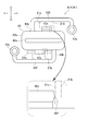
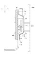
- FIG. 7A It is a perspective view which shows an example of the electronic device proposed in this disclosure. It is a perspective view of a front panel and a power supply unit. It is a figure which shows the rear side of the front panel. It is a top view of the front panel, a button, and an antenna (a view facing the direction shown by IV in FIG. 3). It is an enlarged view of the region IVb shown in FIG. 4A. It is sectional drawing obtained by the VV line in FIG. It is a front view of a button. It is a side view of a button. It is a plan view of a button. It is a front view of a connector board and a shield covering it. It is a bottom view of the connector board and the like shown in FIG. 7A (the view facing the direction shown by B in FIG. 7A). It is sectional drawing obtained by the VIIc-VIIc line shown in FIG. 7A.
- FIG. 1 the electronic device 1 is shown as an example of the embodiment.
- X1 and X2 shown in FIG. 1 will be referred to as right and left
- Y1 and Y2 will be referred to as front and rear, respectively
- Z1 and Z2 will be referred to as upward and downward, respectively.
- these directions are defined to explain the shapes, relative positional relationships, movements, etc. of the elements (parts, members, and parts) of the electronic device 1, and limit the posture of the electronic device 1 during use. is not it.
- FIG. 1 shows an electronic device 1 in a horizontal position
- the electronic device 1 may be arranged in a vertical position during use.
- the "vertical posture” is a posture in which the right side or the left side of the electronic device 1 is on the lower side.
- the electronic device 1 is, for example, an entertainment device that functions as a game device or an audio / visual device.
- the electronic device 1 outputs video / audio data generated by executing a game program, video / audio data acquired through a network, and video / audio data acquired from a recording medium such as an optical disk to a display device such as a television.
- the electronic device may be, for example, a personal computer. Further, it may be a monitor device such as a television, a digital camera, or a server device, and is a device having a button manually operated by a user.
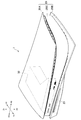
- the electronic device 1 has an exterior member 20.
- the exterior member 20 has, for example, an upper panel 20A forming the upper surface of the electronic device 1 and a lower panel 20B forming the lower surface of the electronic device 1. Further, the exterior member 20 has a front panel 20C constituting the front surface of the electronic device 1.
- a circuit board for example, a heat radiating device for cooling an integrated circuit such as a CPU (Central Processing Unit), a cooling fan, and the like are housed.
- the power supply unit 30 is shown as an example of the device housed in the exterior member 20.
- the power supply unit 30 uses the electric power received from the external power source to generate driving electric power for the circuit board, the cooling fan, and the like.
- the front panel 20C is arranged on the front side of the power supply unit 30.
- buttons 41A and 41B on the front surface thereof.
- the first button 41A is, for example, a power button for activating the electronic device 1.
- the second button 41B is, for example, an optical disc eject button.
- the electronic device 1 has a built-in optical disk drive, and the optical disk can be taken out from the insertion slot 23 (see FIG. 1) in response to the operation of the second button 41B.
- the functions of the buttons 41A and 41B are not limited to the examples described here.
- the electronic device 1 does not have to have an optical disk drive.
- the number of buttons possessed by the electronic device 1 may be one (power button).
- the two buttons 41A and 41B are arranged side by side, for example, in the left-right direction.
- the arrangement of the buttons 41A and 41B is not limited to the example shown in the figure.
- the first button 41A may be provided on the upper surface of the electronic device 1 and the second button 41B may be provided on the front surface.
- Buttons 41A and 41B have almost the same structure. In the following, 41 is used as a button code in the description that does not distinguish between the two buttons 41A and 41B.
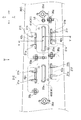
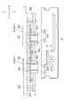
- the electronic device 1 has a circuit board 51 as shown in FIGS. 4A and 5.
- the circuit board 51 is electrically connected to a circuit board (main board) on which a CPU or the like is mounted via, for example, a flat cable.
- the front panel 20C is arranged so as to cover the front surface 51a of the circuit board 51.
- Two switches 52 which are operated by two buttons 41A and 41B, are mounted on the front surface 51a of the circuit board 51.
- the switch 52 is a switch that can be switched between an on state and an off state by a push operation.
- As the switch 52 for example, a membrane switch, a tactile switch, or the like can be used.
- the button 41 has a button movable portion 42 located in front of the switch 52, and elastic portions 43E and 43F extending from the button movable portion 42 and connected to the front panel 20C.
- the button movable portion 42 can move in the thickness direction of the circuit board 51 (the front-back direction in the electronic device 1).
- the elastic portions 43E and 43F support the button movable portion 42 so that the button movable portion 42 can move.
- Buttons 41A and 41B are made of an insulating material. As the insulating material, for example, polycarbonate or ABS resin can be used. Buttons 41A and 41B may be made of two kinds of materials.
- the buttons 41A and 41B may be integrally formed of resin, or may be composed of a plurality of parts connected to each other by a fixture such as a screw or a bolt.
- the front panel 20C is formed with an opening 20a that penetrates the front panel 20C in the front-rear direction.
- the button movable portion 42 has an operated portion 42a that is exposed from the opening 20a toward the front side of the electronic device 1.
- the button movable portion 42 has a base portion 42b arranged along the rear surface of the front panel 20C.
- the operated portion 42a projects forward from the front surface of the base portion 42b.
- the operated portion 42a is fitted inside the opening 20a formed in the front panel 20C, and the front end of the operated portion 42a slightly exceeds the front surface of the front panel 20C.
- a push portion 42c projecting rearward may be formed on the rear surface of the button movable portion 42.
- the push portion 42c is located in front of the switch 52.
- the button movable portion 42 receives a pressing operation from the user, the pressing portion 42c presses the switch 52.
- the button movable portion 42 does not have to have the push portion 42c. In this case, the button movable portion 42 may press the switch 52 on the rear surface.
- the button 41 has a guided portion 42e (see FIGS. 6B and 6C) that moves together with the button movable portion 42.
- two guided portions 42e are formed on the upper edge and the lower edge of the button movable portion 42, respectively.
- the two guided portions 42e face each other with the movable button portion 42 in between.
- the electronic device 1 has guide portions 21E and 21F (see FIG. 5) arranged along the two guided portions 42e, respectively.
- the guided portion 42e moves along the guide portions 21E and 21F in the thickness direction (front-back direction) of the circuit board 51. As a result, the moving direction of the button movable portion 42 is restricted.
- each guide portion 21E / 21F has two side portions 21a / 21b (FIG. 4A) that are separated in the left-right direction, and is between the two side portions 21a / 21b.
- the guided portion 42e is arranged. As shown in FIG. 6B or the like, the guided portion 42e may be integrally molded with the button movable portion 42, or may be molded separately from the button movable portion 42 so as to move together with the button movable portion 42. It may be attached to the button movable portion 42.
- the guide portions 21E and 21F are formed on the front panel 20C and extend rearward from the front panel 20C.
- the front panel 20C has two guide portions 21E and 21F for each of the two buttons 41A and 41B.
- the two guide portions 21E and 21F provided on one button 41 are formed so as to be separated from each other in the vertical direction, for example, in accordance with the two guided portions 42e (see FIG. 5).
- the position of the guided portion 42e may not be the upper edge and the lower edge of the button movable portion 42, but may be the left edge and the right edge of the button movable portion 42.
- the positions of the guide portions 21E and 21F may be formed in accordance with the positions of the guided portions 42e.
- the guide portions 21E / 21F extend rearward from the front panel 20C, and the rear end of the guide portions 21E / 21F is located rearward from the front surface 51a of the circuit board 51.
- the guide portions 21E and 21F extend rearward beyond the position of the rear surface 51b of the circuit board 51, and the rear ends of the guide portions 21E and 21F are located rearward of the rear surface 51b of the circuit board 51. ing. Since the guide portions 21E and 21F extend rearward from the front panel 20C in this way, the portion located in front of the front surface 51a of the circuit board 51 and the portion located behind the rear surface 51b of the circuit board 51 can be separated from each other. Have.
- the guided portion 42e extends rearward from the base portion 42b of the button movable portion 42 beyond the rear surface 51b of the circuit board 51.
- the guided portion 42e also has a portion located behind the rear surface 51b of the circuit board 51.
- the guided portion 42e is guided by the guide portions 21E and 21F at a position behind the rear surface 51b of the circuit board 51.
- the rear end of the guided portion 42e may be located slightly rearward of the rear ends of the guide portions 21E and 21F.
- the guide portions 21E and 21F it is possible to effectively suppress the tilting of the button movable portion 42. Specifically, since the distance from the opening 20a formed in the front panel 20C to the rear ends of the guide portions 21E and 21F in the front-rear direction becomes large, the rear end of the button 41 (the rear end of the guided portion 42e) For example, the position is prevented from shifting to the left or right, and as a result, the inclination of the button movable portion 42 is effectively suppressed. In addition, the lengths of the guide portions 21E and 21F in the front-rear direction increase. This can also contribute to suppressing the tilting of the movable portion 42.
- the antenna 31 is arranged behind the circuit board 51.
- the antenna 31 is attached to the front surface of the power supply unit 30 arranged behind the circuit board 51.
- the distance D1 in the front-rear direction from the front surface 51a of the circuit board 51 to the antenna 31 is larger than the distance D2 in the front-rear direction from the rear ends (contact portions 21c described later) of the guide portions 21E and 21F to the antenna 31. According to this structure, it is possible to suppress the generation of noise in the signal transmitted / received through the antenna 31 due to the signal flowing through the circuit board 51, for example.
- the rear ends of the guide portions 21E and 21F are located behind the rear surface 51b of the circuit board 51. Therefore, the distance from the rear surface 51b of the circuit board 51 to the antenna 31 in the front-rear direction is also larger than the distance D2 in the front-rear direction from the rear ends of the guide portions 21E / 21F to the antenna 31.
- the electrical component arranged behind the circuit board 51 does not have to be an antenna. In this case, it is possible to suppress the generation of noise in the signal flowing through the electric component due to the signal flowing through the circuit board 51.
- the distance D3 in the front-rear direction from the front surface 51a of the circuit board 51 to the rear ends (contact portions 21c described later) of the guide portions 21E and 21F may be larger than the thickness T1 of the front panel 20C. ..
- the distance D3 in the front-rear direction from the front surface 51a of the circuit board 51 to the rear ends (contact portions 21c described later) of the guide portions 21E and 21F is larger than the movable range of the button movable portion 42. You may.
- the guide portions 21E and 21F may be formed of a member different from that of the front panel 20C.
- the guide portions 21E and 21F may be formed on a member arranged behind the circuit board 51, or may be formed on a member attached to the circuit board 51. In this case, the guide portions 21E and 21F do not have to have a portion located in front of the circuit board 51.
- each guide portion 21E / 21F may have two side portions 21a / 21b separated in the left-right direction.
- the side portions 21a and 21b may extend rearward from the front panel 20C.
- Each guided portion 42e is sandwiched between two side portions 21a and 21b. As a result, the tilting of the button movable portion 42 can be effectively suppressed.
- the operated portion 42a of the button 41 has an elongated shape in the left-right direction (see FIG. 2). Therefore, the user may press only the right portion of the operated portion 42a, or may press only the left portion of the operated portion 42a. Even in such a case, the two side portions 21a and 21b sandwiching the guided portion 42e can effectively prevent the button movable portion 42 from tilting to the left or right.
- the guided portion 42e may be composed of two side portions separated in the left-right direction. Then, the guide portions 21E and 21F may be arranged between the two side portions. Even in this structure, it is possible to effectively prevent the button movable portion 42 from tilting to the left or right.
- the guide portions 21E and 21F may be formed with contact portions 21c that protrude toward the guided portion 42e and are located behind the rear surface 51b of the circuit board 51.
- the guide portions 21E and 21F may come into contact with the guided portion 42e at the contact portion 21c.
- contact portions 21c projecting inward are formed on each of the two side portions 21a and 21b (see FIG. 4A) constituting the guide portions 21E and 21F.
- the side portions 21a and 21b are in contact with the side surface of the guided portion 42e at the contact portion 21c.
- the contact portion 21c may extend in the vertical direction at the rear ends of the side portions 21a and 21b.
- contact portions 42f protruding to the right and left may be formed on the right side surface and the left side surface of the guided portion 42e.
- the contact portion 42f extends in the front-rear direction.
- the contact portions 21c of the guide portions 21E and 21F may be in contact with the contact portion 42f of the guided portion 42e. According to this structure, the contact area between the guide portions 21E and 21F and the guided portion 42e can be reduced.
- the contact portions extending in the front-rear direction may be formed on the guide portions 21E and 21F.
- the button 41 may have a contact portion located at the rear end of the guided portion 42e on the right side surface and the left side surface of the guided portion 42e, respectively.
- the guided portion 42e is formed on the upper edge and the lower edge of the button movable portion 42 as described above. As shown in FIG. 5, the circuit board 51 is arranged between the two guided portions 42e. The upper guided portion 42e extends rearward beyond the position of the upper edge of the circuit board 51. The lower guided portion 42e extends rearward beyond the position of the lower edge of the circuit board 51. As shown in FIG. 3, the positions of the two guided portions 42e may be displaced in the left-right direction, or their positions in the left-right direction may be the same.
- the circuit board 51 extends in the left-right direction between the two guided portions 42e of the first button 41A and between the two guided portions 42e of the second button 41B. Both ends of the circuit board 51 are attached to two bosses (mounting portions) 20d formed on the front panel 20C (see FIG. 4A).
- the positional relationship between the circuit board 51 and the guided portion 42e is not limited to the example of the electronic device 1.
- an opening that penetrates the circuit board 51 in the front-rear direction may be formed in the circuit board 51.
- the guided portion 42e may pass through the inside of this opening and extend rearward.
- the guide portions 21E and 21F may also pass through the inside of the opening of the circuit board 51 and extend rearward.
- the button 41 has elastic portions 43E and 43F.
- the elastic portions 43E and 43F are arranged point-symmetrically with respect to the center of the button movable portion 42.
- Each of the elastic portions 43E and 43F has a fixing portion 43a attached to a boss 20g (attachment portion, see FIG. 3) formed on the rear surface of the front panel 20C at its end.
- the base portions 43b of the elastic portions 43E and 43F are connected to the upper edge and the lower edge of the base portion 42b of the button movable portion 42, respectively.
- the base portion 43b and the fixing portion 43a are located on opposite sides of the guided portions 42e and 42f.
- the elastic portions 43E and 43F have a substantially U-shape when the button 41 is viewed in the front-rear direction, and extend in the left-right direction beyond the positions of the guided portions 42e and 42f. According to this, it is possible to secure a sufficient length of the elastic portions 43E and 43F, and it becomes easy to secure the movable range of the button movable portion 42.
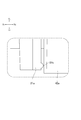
- the electronic device 1 has connectors 61A and 61B on the front surface thereof.
- a circuit board 60 is arranged behind the front panel 20C along the front panel 20C (see FIG. 7B).
- the connectors 61A and 61B are mounted on the front surface 60a of the circuit board 60.
- a flexible flat cable 63 is connected to the circuit board 60. As shown in FIG. 7C, one end of the flat cable 63 is connected to a connector 64 mounted on the front surface 60a of the circuit board 60.
- the connector 64 has an insertion port 64a on the lower surface thereof into which the flat cable 63 is inserted.
- the insertion port 64a opens in the direction along the circuit board 60 (downward in the example shown in the figure), and the flat cable 63 extends in the direction along the circuit board 60 from the end connected to the insertion port 64a. ing.
- the circuit board 60 is connected to a circuit board (main board) on which an integrated circuit such as a CPU is mounted via the flat cable 63.
- the electronic device 1 has a shield 71 that covers the front surface 60a of the circuit board 60.
- the shield 71 may be attached to the circuit board 60 by a fixture such as a screw.
- the connector 64 to which the flat cable 63 is connected is also covered with the shield 71.
- the shield 71 has a concave edge portion 71b that forms an opening through which the flat cable 63 passes together with the front surface 60a of the circuit board 60.
- the distance D6 from the front surface 60a of the circuit board 60 to the concave edge portion 71b is lower than the height H1 of the insertion port 64a with reference to the front surface 60a of the circuit board 60.
- the height H1 is the distance from the front surface 60a of the circuit board 60 to the front edge of the insertion port 64a.
- the flat cable 63 extends obliquely from the insertion port 64a toward the front surface 60a of the circuit board 60. According to this structure of the shield 71, since the gap formed between the flat cable 63 and the concave edge portion 71b is small, the generation of unnecessary radiation from the circuit board 60 can be effectively suppressed.
- the distance D6 from the front surface 60a of the circuit board 60 to the concave edge portion 71b corresponds to the thickness of the flat cable 63. Therefore, the concave edge portion 71b may be in contact with the flat cable 63.
- the width W1 of the concave edge portion 71b in the left-right direction corresponds to the width of the flat cable 63.
- the shield 71 is in contact with the front surface 60a of the circuit board 60 on the right side and the left side of the concave edge portion 71b.
- the shield 71 extends diagonally from the main plate portion 71c located in front of the connector 64 and covering the main plate portion 71c from the main plate portion 71c to the concave edge portion 71b toward the front surface 60a of the circuit board 60. It has an inclined portion 71e. The inclined portion 71e extends to the concave edge portion 71b while being curved. The concave edge portion 71b further extends in the direction along the front surface 60a of the circuit board 60.
- the shield 71 has a rear surface 71f facing the circuit board 60. A part of the rear surface 71f functions as a concave edge portion 71b. Due to this shape of the shield 71, the load acting on the flat cable 63 can be reduced even when a force for pushing the front surface of the shield 71 in the direction toward the circuit board 60 is applied.
- the shield 71 has a contact region 71g around the main plate portion 71c that surrounds the connector 64 and is in contact with the front surface 60a of the circuit board 60.
- the contact region 71g may be in contact with the ground region formed on the front surface 60a of the circuit board 60.
- the shield 71 has openings 71h / 71i (see FIG. 7A) at the positions of the connectors 61A / 61B, and the connectors 61A / 61B project from the openings 71h / 71i to the outside (front side) of the shield 71.
- buttons 41A and 41B have a button movable portion 42 that is arranged in front of the circuit board 51 and is allowed to move in the front-rear direction, and a guided portion 42e that moves together with the button movable portion 42.
- the switch 52 of the circuit board 51 is operated by the button movable portion 42.
- the guide portions 21E and 21F are arranged along the guided portion 42e and regulate the moving direction of the button movable portion 42.
- the guide portions 21E and 21F and the guided portion 42e have portions located behind the front surface 51a of the circuit board 51.
- the distance from the opening 20a formed in the front panel 20C to the rear ends of the guide portions 21E and 21F in the front-rear direction becomes large, so that the rear end of the button 41 (rear end of the guided portion 42e)
- the position of the button is prevented from shifting to the left or right, and as a result, the inclination of the button movable portion 42 is effectively suppressed.
- the electronic device proposed in the present disclosure is not limited to the structure of the electronic device 1 described above, and various modifications can be made.
- the positions of the guide portions 21E and 21F with respect to the button movable portion 42 are not limited to the example of the electronic device 1.
- the guide portions 21E and 21F may be formed on the right side and the left side of the button movable portion 42, respectively.
Landscapes
- Engineering & Computer Science (AREA)
- Microelectronics & Electronic Packaging (AREA)
- Push-Button Switches (AREA)
Priority Applications (2)
| Application Number | Priority Date | Filing Date | Title |
|---|---|---|---|
| US17/910,203 US12462992B2 (en) | 2020-03-27 | 2021-03-23 | Electronic device |
| JP2022510541A JP7660558B2 (ja) | 2020-03-27 | 2021-03-23 | 電子機器 |
Applications Claiming Priority (2)
| Application Number | Priority Date | Filing Date | Title |
|---|---|---|---|
| JP2020-059188 | 2020-03-27 | ||
| JP2020059188 | 2020-03-27 |
Publications (1)
| Publication Number | Publication Date |
|---|---|
| WO2021193623A1 true WO2021193623A1 (ja) | 2021-09-30 |
Family
ID=77892198
Family Applications (1)
| Application Number | Title | Priority Date | Filing Date |
|---|---|---|---|
| PCT/JP2021/011969 Ceased WO2021193623A1 (ja) | 2020-03-27 | 2021-03-23 | 電子機器 |
Country Status (3)
| Country | Link |
|---|---|
| US (1) | US12462992B2 (https=) |
| JP (1) | JP7660558B2 (https=) |
| WO (1) | WO2021193623A1 (https=) |
Families Citing this family (1)
| Publication number | Priority date | Publication date | Assignee | Title |
|---|---|---|---|---|
| JP7273149B2 (ja) * | 2019-05-23 | 2023-05-12 | 株式会社ソニー・インタラクティブエンタテインメント | 電子機器 |
Citations (1)
| Publication number | Priority date | Publication date | Assignee | Title |
|---|---|---|---|---|
| JPH02172115A (ja) * | 1988-12-26 | 1990-07-03 | Omron Tateisi Electron Co | キーボードスイッチ |
Family Cites Families (6)
| Publication number | Priority date | Publication date | Assignee | Title |
|---|---|---|---|---|
| JPS6355338U (https=) | 1986-09-29 | 1988-04-13 | ||
| JP2005183306A (ja) * | 2003-12-22 | 2005-07-07 | T An T:Kk | プッシュスイッチの押しボタン構造 |
| US7592559B2 (en) * | 2005-04-28 | 2009-09-22 | Trw Automotive U.S. Llc | Bezel and actuator |
| CN103367006B (zh) * | 2012-04-05 | 2015-09-09 | 光宝电子(广州)有限公司 | 薄型按键结构及薄型键盘 |
| JP5889852B2 (ja) | 2013-09-18 | 2016-03-22 | 株式会社ソニー・コンピュータエンタテインメント | 電子機器 |
| TWI756626B (zh) * | 2020-02-06 | 2022-03-01 | 達方電子股份有限公司 | 按鍵結構及鍵盤 |
-
2021
- 2021-03-23 WO PCT/JP2021/011969 patent/WO2021193623A1/ja not_active Ceased
- 2021-03-23 US US17/910,203 patent/US12462992B2/en active Active
- 2021-03-23 JP JP2022510541A patent/JP7660558B2/ja active Active
Patent Citations (1)
| Publication number | Priority date | Publication date | Assignee | Title |
|---|---|---|---|---|
| JPH02172115A (ja) * | 1988-12-26 | 1990-07-03 | Omron Tateisi Electron Co | キーボードスイッチ |
Also Published As
| Publication number | Publication date |
|---|---|
| JPWO2021193623A1 (https=) | 2021-09-30 |
| US20230110303A1 (en) | 2023-04-13 |
| JP7660558B2 (ja) | 2025-04-11 |
| US12462992B2 (en) | 2025-11-04 |
Similar Documents
| Publication | Publication Date | Title |
|---|---|---|
| JP5169777B2 (ja) | 携帯端末装置 | |
| JP5638484B2 (ja) | 電子機器 | |
| JP5589020B2 (ja) | 電子機器 | |
| CN101861066B (zh) | 电子设备 | |
| JP6474763B2 (ja) | 電子機器 | |
| JP2000122793A (ja) | キーボード及び情報処理装置 | |
| CN1910542A (zh) | 手指可控制的多向开关 | |
| US10367299B2 (en) | Plug connector assembly with an unlocking apparatus for unlocking a latch | |
| JP2011128986A (ja) | 電子機器 | |
| JP5518806B2 (ja) | 電子機器 | |
| WO2021193623A1 (ja) | 電子機器 | |
| US10405449B2 (en) | Electronic apparatus | |
| JP2010212172A (ja) | プッシュオンスイッチ | |
| JP5314740B2 (ja) | 電子機器 | |
| JP7820567B2 (ja) | 光ディスクドライブ、電子機器ユニット | |
| JP7807611B1 (ja) | 装置 | |
| JP7823228B2 (ja) | 接続構造、光ディスクドライブ | |
| JP2012059728A (ja) | 光モジュール | |
| WO2024176921A1 (ja) | 電子機器及び外装パネル | |
| WO2026028405A1 (ja) | 装置 | |
| JP5228901B2 (ja) | プッシュオンスイッチ | |
| JP2004006120A (ja) | 操作キー装置及び電子機器 | |
| JP2020053658A (ja) | 電子機器ユニットおよび電子機器 | |
| JP2017103167A (ja) | 押圧式スイッチ装置、及び電子機器 | |
| JP2012038527A (ja) | コネクタアッセンブリ |
Legal Events
| Date | Code | Title | Description |
|---|---|---|---|
| 121 | Ep: the epo has been informed by wipo that ep was designated in this application |
Ref document number: 21776547 Country of ref document: EP Kind code of ref document: A1 |
|
| ENP | Entry into the national phase |
Ref document number: 2022510541 Country of ref document: JP Kind code of ref document: A |
|
| NENP | Non-entry into the national phase |
Ref country code: DE |
|
| 122 | Ep: pct application non-entry in european phase |
Ref document number: 21776547 Country of ref document: EP Kind code of ref document: A1 |
|
| WWG | Wipo information: grant in national office |
Ref document number: 17910203 Country of ref document: US |