WO2021193202A1 - 熱処理装置及び熱処理方法 - Google Patents
熱処理装置及び熱処理方法 Download PDFInfo
- Publication number
- WO2021193202A1 WO2021193202A1 PCT/JP2021/010419 JP2021010419W WO2021193202A1 WO 2021193202 A1 WO2021193202 A1 WO 2021193202A1 JP 2021010419 W JP2021010419 W JP 2021010419W WO 2021193202 A1 WO2021193202 A1 WO 2021193202A1
- Authority
- WO
- WIPO (PCT)
- Prior art keywords
- gas
- substrate
- heat treatment
- gas supply
- wafer
- Prior art date
Links
Images


Classifications
-
- G—PHYSICS
- G03—PHOTOGRAPHY; CINEMATOGRAPHY; ANALOGOUS TECHNIQUES USING WAVES OTHER THAN OPTICAL WAVES; ELECTROGRAPHY; HOLOGRAPHY
- G03F—PHOTOMECHANICAL PRODUCTION OF TEXTURED OR PATTERNED SURFACES, e.g. FOR PRINTING, FOR PROCESSING OF SEMICONDUCTOR DEVICES; MATERIALS THEREFOR; ORIGINALS THEREFOR; APPARATUS SPECIALLY ADAPTED THEREFOR
- G03F7/00—Photomechanical, e.g. photolithographic, production of textured or patterned surfaces, e.g. printing surfaces; Materials therefor, e.g. comprising photoresists; Apparatus specially adapted therefor
- G03F7/26—Processing photosensitive materials; Apparatus therefor
- G03F7/38—Treatment before imagewise removal, e.g. prebaking
-
- G—PHYSICS
- G03—PHOTOGRAPHY; CINEMATOGRAPHY; ANALOGOUS TECHNIQUES USING WAVES OTHER THAN OPTICAL WAVES; ELECTROGRAPHY; HOLOGRAPHY
- G03F—PHOTOMECHANICAL PRODUCTION OF TEXTURED OR PATTERNED SURFACES, e.g. FOR PRINTING, FOR PROCESSING OF SEMICONDUCTOR DEVICES; MATERIALS THEREFOR; ORIGINALS THEREFOR; APPARATUS SPECIALLY ADAPTED THEREFOR
- G03F7/00—Photomechanical, e.g. photolithographic, production of textured or patterned surfaces, e.g. printing surfaces; Materials therefor, e.g. comprising photoresists; Apparatus specially adapted therefor
- G03F7/004—Photosensitive materials
- G03F7/0042—Photosensitive materials with inorganic or organometallic light-sensitive compounds not otherwise provided for, e.g. inorganic resists
-
- G—PHYSICS
- G03—PHOTOGRAPHY; CINEMATOGRAPHY; ANALOGOUS TECHNIQUES USING WAVES OTHER THAN OPTICAL WAVES; ELECTROGRAPHY; HOLOGRAPHY
- G03F—PHOTOMECHANICAL PRODUCTION OF TEXTURED OR PATTERNED SURFACES, e.g. FOR PRINTING, FOR PROCESSING OF SEMICONDUCTOR DEVICES; MATERIALS THEREFOR; ORIGINALS THEREFOR; APPARATUS SPECIALLY ADAPTED THEREFOR
- G03F7/00—Photomechanical, e.g. photolithographic, production of textured or patterned surfaces, e.g. printing surfaces; Materials therefor, e.g. comprising photoresists; Apparatus specially adapted therefor
- G03F7/26—Processing photosensitive materials; Apparatus therefor
-
- H—ELECTRICITY
- H01—ELECTRIC ELEMENTS
- H01L—SEMICONDUCTOR DEVICES NOT COVERED BY CLASS H10
- H01L21/00—Processes or apparatus adapted for the manufacture or treatment of semiconductor or solid state devices or of parts thereof
- H01L21/02—Manufacture or treatment of semiconductor devices or of parts thereof
- H01L21/027—Making masks on semiconductor bodies for further photolithographic processing not provided for in group H01L21/18 or H01L21/34
- H01L21/0271—Making masks on semiconductor bodies for further photolithographic processing not provided for in group H01L21/18 or H01L21/34 comprising organic layers
- H01L21/0273—Making masks on semiconductor bodies for further photolithographic processing not provided for in group H01L21/18 or H01L21/34 comprising organic layers characterised by the treatment of photoresist layers
- H01L21/0274—Photolithographic processes
- H01L21/0275—Photolithographic processes using lasers
-
- H—ELECTRICITY
- H01—ELECTRIC ELEMENTS
- H01L—SEMICONDUCTOR DEVICES NOT COVERED BY CLASS H10
- H01L21/00—Processes or apparatus adapted for the manufacture or treatment of semiconductor or solid state devices or of parts thereof
- H01L21/67—Apparatus specially adapted for handling semiconductor or electric solid state devices during manufacture or treatment thereof; Apparatus specially adapted for handling wafers during manufacture or treatment of semiconductor or electric solid state devices or components ; Apparatus not specifically provided for elsewhere
- H01L21/67005—Apparatus not specifically provided for elsewhere
- H01L21/67011—Apparatus for manufacture or treatment
- H01L21/67098—Apparatus for thermal treatment
- H01L21/67103—Apparatus for thermal treatment mainly by conduction
-
- H—ELECTRICITY
- H01—ELECTRIC ELEMENTS
- H01L—SEMICONDUCTOR DEVICES NOT COVERED BY CLASS H10
- H01L21/00—Processes or apparatus adapted for the manufacture or treatment of semiconductor or solid state devices or of parts thereof
- H01L21/67—Apparatus specially adapted for handling semiconductor or electric solid state devices during manufacture or treatment thereof; Apparatus specially adapted for handling wafers during manufacture or treatment of semiconductor or electric solid state devices or components ; Apparatus not specifically provided for elsewhere
- H01L21/67005—Apparatus not specifically provided for elsewhere
- H01L21/67011—Apparatus for manufacture or treatment
- H01L21/67098—Apparatus for thermal treatment
- H01L21/67109—Apparatus for thermal treatment mainly by convection
-
- H—ELECTRICITY
- H01—ELECTRIC ELEMENTS
- H01L—SEMICONDUCTOR DEVICES NOT COVERED BY CLASS H10
- H01L21/00—Processes or apparatus adapted for the manufacture or treatment of semiconductor or solid state devices or of parts thereof
- H01L21/67—Apparatus specially adapted for handling semiconductor or electric solid state devices during manufacture or treatment thereof; Apparatus specially adapted for handling wafers during manufacture or treatment of semiconductor or electric solid state devices or components ; Apparatus not specifically provided for elsewhere
- H01L21/67005—Apparatus not specifically provided for elsewhere
- H01L21/67011—Apparatus for manufacture or treatment
- H01L21/67155—Apparatus for manufacturing or treating in a plurality of work-stations
- H01L21/67161—Apparatus for manufacturing or treating in a plurality of work-stations characterized by the layout of the process chambers
- H01L21/67178—Apparatus for manufacturing or treating in a plurality of work-stations characterized by the layout of the process chambers vertical arrangement
-
- H—ELECTRICITY
- H01—ELECTRIC ELEMENTS
- H01L—SEMICONDUCTOR DEVICES NOT COVERED BY CLASS H10
- H01L21/00—Processes or apparatus adapted for the manufacture or treatment of semiconductor or solid state devices or of parts thereof
- H01L21/67—Apparatus specially adapted for handling semiconductor or electric solid state devices during manufacture or treatment thereof; Apparatus specially adapted for handling wafers during manufacture or treatment of semiconductor or electric solid state devices or components ; Apparatus not specifically provided for elsewhere
- H01L21/683—Apparatus specially adapted for handling semiconductor or electric solid state devices during manufacture or treatment thereof; Apparatus specially adapted for handling wafers during manufacture or treatment of semiconductor or electric solid state devices or components ; Apparatus not specifically provided for elsewhere for supporting or gripping
- H01L21/687—Apparatus specially adapted for handling semiconductor or electric solid state devices during manufacture or treatment thereof; Apparatus specially adapted for handling wafers during manufacture or treatment of semiconductor or electric solid state devices or components ; Apparatus not specifically provided for elsewhere for supporting or gripping using mechanical means, e.g. chucks, clamps or pinches
- H01L21/68714—Apparatus specially adapted for handling semiconductor or electric solid state devices during manufacture or treatment thereof; Apparatus specially adapted for handling wafers during manufacture or treatment of semiconductor or electric solid state devices or components ; Apparatus not specifically provided for elsewhere for supporting or gripping using mechanical means, e.g. chucks, clamps or pinches the wafers being placed on a susceptor, stage or support
- H01L21/68742—Apparatus specially adapted for handling semiconductor or electric solid state devices during manufacture or treatment thereof; Apparatus specially adapted for handling wafers during manufacture or treatment of semiconductor or electric solid state devices or components ; Apparatus not specifically provided for elsewhere for supporting or gripping using mechanical means, e.g. chucks, clamps or pinches the wafers being placed on a susceptor, stage or support characterised by a lifting arrangement, e.g. lift pins
Definitions
- the present disclosure relates to a heat treatment apparatus and a heat treatment method.
- a resist is applied onto a semiconductor wafer (hereinafter referred to as "wafer") to form a resist film.
- the wafer on which the resist film is formed is subjected to an exposure process for exposing a predetermined circuit pattern.
- the chemical reaction of the exposed portion or the unexposed portion of the resist film proceeds and becomes soluble or insoluble in the developing solution.
- the soluble portion of the resist film is removed and a predetermined resist pattern is formed on the wafer.
- the solubility of an exposed portion or an unexposed portion in a developing solution changes when it is heated by reacting with water.
- a substrate having an exposed resist film formed on its surface whose solubility in a developing solution in an exposed portion or an unexposed portion changes when heated by reacting with water, is placed and heated.
- Stage and An elevating mechanism for relatively elevating and lowering the substrate between a first position on which the substrate is placed and a second position away from the stage.
- a gas supply unit that supplies a first gas having a higher humidity than the atmosphere in which the stage is provided to the substrate located at the second position before moving to the first position. Equipped with.
- the solubility of an exposed or unexposed portion in a developing solution changes when heated by reacting with water when a substrate on which an exposed resist is formed is heat-treated.
- the heat treatment apparatus 1 is an apparatus for heating the wafer W on which the resist film is formed, and the resist film is exposed along the circuit pattern by, for example, EUV. Therefore, the heat treatment apparatus 1 is an apparatus that performs so-called post-exposure baking (PEB).
- the resist constituting this resist film contains, for example, a metal, and tin is an example of the metal.
- the ligand is desorbed from the metal by irradiation with the above radiation such as EUV, and the resist reacts with water in that state to introduce a hydroxyl group. Subsequent heating causes dehydration condensation between the hydroxyl groups, resulting in insolubilization in the developing solution.
- the heat treatment apparatus 1 performs the above-mentioned introduction of hydroxyl groups (hydrophilization treatment) and dehydration condensation. Therefore, as a result of the treatment by the heat treatment apparatus 1, the exposed region of the resist film is insoluble in the developing solution, the unexposed region is dissolved in the developing solution and removed, and a pattern is formed on the resist film. NS.
- the configuration of the heat treatment apparatus 1 will be described with reference to the longitudinal side view of FIG.
- the heat treatment apparatus 1 includes a housing 10, and a wafer W transfer port 10A is provided on the side wall of the housing 10. Further, the heat treatment apparatus 1 is provided in an air atmosphere, and the inside and outside of the housing 10 are the air atmosphere.
- a chamber (processing chamber) 20 for heat-treating the wafer W is provided on the back side of the housing 10 when viewed from the side where the transport port 10A is open.
- the processing chamber 20 includes a lid portion 21 that constitutes a ceiling portion, and a lower side portion 22 that is located on the lower side of the lid portion 21 and includes a bottom portion.
- the lid portion 21 forming the upper portion of the processing chamber 20 is connected to the elevating mechanism 28 for the chamber via the support portion 29. Then, the elevating mechanism 28 raises the lid 21 with respect to the lower side 22 to separate and open the processing chamber 20, and lowers the lid 21 to close the processing chamber 20.
- a stage 23 is provided inside the lower side portion 22.
- Reference numeral 25 in FIG. 1 is a holding member for holding the stage 23.
- a heater 24 is embedded in the stage 23, and the wafer W placed on the stage 23 is configured to be heated at, for example, 50 ° C. to 210 ° C.
- the stage 23 is provided with three through holes 23a in the circumferential direction that penetrate the stage 23 in the thickness direction.
- a vertical elevating pin 26 is inserted through each through hole 23a.
- Each elevating pin 26 is connected to an elevating mechanism 27 installed at the bottom of the lower portion 22. Further, each elevating pin 26 is elevated and lowered by the elevating mechanism 27, and the tip of the elevating pin 26 is recessed on the surface of the stage 23.
- the wafer W is moved up and down between the first position mounted on the stage 23 and the second position away from the stage 23 by the elevating pin 26 recessed on the surface of the stage 23.
- the heat treatment apparatus 1 includes a gas supply unit 3 for supplying moist air containing moisture to the wafer W to surely hydrophilize the resist film and promote dehydration condensation.
- the gas supply unit 3 is provided inside the lid portion 21 and includes a shower head 30 which is an opposing portion having an facing surface facing the wafer W mounted on the stage 23.
- the inside of the shower head 30 is a diffusion space for diffusing gas. Further, on the lower surface of the shower head 30 (the surface facing the wafer W), gas discharge holes 31 for supplying gas toward the wafer W are dispersed and formed on the entire surface.
- One end of the gas supply pipe 32 is connected to the upper surface of the shower head 30 so as to communicate with the diffusion space.
- a gas supply source 33 for supplying a first gas having a higher humidity than the atmosphere in which the stage 23 is provided is provided via a valve V32.
- the first gas is, for example, moist air having a humidity of 68%. Humidity used in the present specification indicates relative humidity.
- the atmosphere in which the stage 23 is provided refers to the atmosphere above the stage 23 when the first gas is not supplied from the gas supply unit 3 toward the wafer W. Therefore, the first gas, which is the above-mentioned moist air, is a gas for increasing the humidity of the atmosphere above the stage 23.
- the gas supply source 33 for example, a module capable of adjusting the moisture contained in the air to supply air having a desired humidity is used.
- a module capable of adjusting the moisture contained in the air to supply air having a desired humidity is used.
- it includes a bubbler, a first line for supplying water vapor generated by the bubbler to the downstream side, and a second line for supplying and mixing an arbitrary flow rate of air to the water vapor flowing through the first line.
- the gas supply source 33 can be configured as described above. Then, by adjusting the flow rate of air in the second line, air having a desired humidity can be supplied to the shower head 30.
- the configuration is not limited to such a configuration, and the configuration of the gas supply source 33 can be any configuration.
- a central exhaust port 34 for exhausting the atmosphere inside the processing chamber 20 is opened in the center of the lower surface of the shower head 30.
- a central exhaust pipe 341 provided so as to penetrate the shower head 30 is connected to the central exhaust port 34.
- the shower head 30 is arranged with a gap between the side peripheral surface and the inner surface of the lid portion 21, and the gap constitutes an outer peripheral side exhaust port 35 for exhausting from the outer peripheral side of the wafer W.
- the outer peripheral side exhaust port 35 communicates with the outer peripheral side exhaust pipe 351.
- the central exhaust pipe 341 and the outer peripheral side exhaust pipe 351 are connected to the exhaust equipment in the factory so that the atmosphere inside the processing chamber 20 can be exhausted.
- the V341 and V351 provided in the central exhaust pipe 341 and the outer peripheral side exhaust pipe 351 are valves for opening and closing the central exhaust pipe 341 and the outer peripheral side exhaust pipe 351 respectively.
- a transport mechanism 11 is provided on the front side (convey port 10A side) in the housing 10.
- the transport mechanism 11 includes a support plate 12 which is a horizontal substantially disk-shaped support portion, and the wafer W is placed on the surface of the support plate 12.
- a temperature control mechanism (not shown) is embedded in the support plate 12, and the temperature of the wafer W placed on the support plate 12 is controlled so as to be uniform in the plane.
- the support plate 12 is moved along a guide rail 15 provided on the bottom surface of the housing 10 from the transport port 10A side toward the back side by a moving mechanism 14 connected via a support member 13. Thereby, the support plate 12 can be moved between the upper region of the stage 23 and the outer region (position shown in FIG. 1) of the processing chamber 20 laterally displaced from the stage 23.
- the transport mechanism 11 When the transport mechanism 11 is located in the outer region, the transport mechanism outside the heat treatment apparatus 1 holding the wafer W enters the housing 10 from the transport port 10A. Further, the external transfer mechanism moves up and down from the upper side to the lower side of the support plate 12, so that the wafer W is transferred between the external transfer mechanism of the heat treatment apparatus 1 and the transfer mechanism 11 in the housing 10.
- the support plate 12 is formed with a slit (not shown) from the end portion on the processing chamber 20 side toward the other end side. When the support plate 12 is positioned on the stage 23 by this slit, the elevating pin 26 protruding from the stage 23 can project onto the support plate 12 through the slit. Then, the wafer W is transferred between the stage 23 and the support plate 12 by the cooperation between the raising and lowering of the raising and lowering pin 26 and the advancement and retreat of the conveying mechanism 11.
- the heat treatment apparatus 1 includes, for example, a control unit 100 including a computer.
- the control unit 100 is configured to be able to output a control signal to the elevating mechanism 28 for the chamber, the elevating mechanism 27, the valves V32, V341, V351, and the moving mechanism 14.
- a command (step group) is set in the control unit 100 so that the wafer W shown in the operation of the heat treatment apparatus 1 described later, the elevating pin 26, the elevating and lowering of the lid portion 21, and the gas supply sequence are executed.
- the program is stored. This program is stored in a storage medium such as a compact disk, a hard disk, an MO (magneto-optical disk), a DVD, or a memory card, and installed in the control unit 100.
- the stage 23 is heated to 50 ° C. to 210 ° C. by the heater 24, and the processing chamber 20 is opened to wait for exhaust from the exhaust ports 34 and 35. Further, the support plate 12 stands by at a position where the wafer W is received (a position shown by a solid line in FIG. 1). First, an external transfer mechanism (not shown) holding the exposed wafer W is introduced into the heat treatment apparatus 1 and moved from above to below the support plate 12 to place the wafer W on the support plate 12.
- the support plate 12 moves the support plate 12 directly above the stage 23. Further, the wafer W supported by the support plate 12 is pushed up by the elevating pin 26 and supported at the second position on the stage 23, and the support plate 12 retracts to the outer region. Subsequently, as shown in FIG. 2, the first gas is supplied toward the wafer W, and for example, exhaust is performed from the outer peripheral side exhaust port 35 of each exhaust port. At this time, the lid portion 21 remains raised and the processing chamber 20 is open. Moisture is supplied to the wafer W by being exposed to the first gas which is moist air, and the resist film is hydrophilized.
- the elevating pin 26 is lowered and the wafer W is placed at the mounting position (first position) of the stage 23. ).
- the lid 21 is lowered in parallel with the lowering of the elevating pin 26 to close the processing chamber 20.
- the wafer W is heated and heat-treated so as to have the same temperature as the stage 23.
- the temperature of the wafer W rises, dehydration condensation of the hydroxyl groups described above occurs, and insolubilization of the exposed portion of the resist film with the developing solution progresses.
- the supply of the first gas is stopped, the exhaust by the outer peripheral side exhaust port 35 is stopped, and the exhaust is switched from the central exhaust port 34.
- the lid portion 21 is raised to open the processing chamber 20, and the elevating pin 26 is raised to raise the wafer W from the stage 23.
- the wafer W is delivered to the transfer mechanism 11 by the cooperation of the transfer mechanism 11 and the elevating pin 26. Further, the wafer W is delivered to an external transfer device, carried out from the heat treatment device 1, and undergoes development processing.
- the heat treatment apparatus 1 air (first gas) having a higher humidity than the atmosphere on the stage 23 is supplied to the wafer W to perform heat treatment. Therefore, during the heat treatment, a hydroxyl group is sufficiently introduced into the exposed portion of the resist film, and the insolubilization of the exposed portion rapidly progresses during the heat treatment. That is, the sensitivity of the reaction due to heating of the exposed portion is increased. Since the insolubilization of the exposed portion is promoted in this way, it is suppressed that the insolubilization is insufficient at the time of the developing process and the width of the convex portion of the resist pattern becomes smaller than the set value.
- the heat of the wafer W reduces the adhesion of the moisture contained in the first gas to the resist film.
- the first gas since the first gas is supplied before being placed on the stage 23, heating is performed in a state where the above-mentioned hydroxyl groups are surely introduced. Therefore, the rapid insolubilization of the exposed portion can be performed with high certainty. Since the position where the first gas is supplied is above the stage 23, the wafer W can be quickly placed on the stage 23 and heat-treated after the introduction of the hydroxyl group.
- drying occurs in the plane of the wafer W under the influence of the air flow in the region where the wafer W moves from the first gas supply to the placement on the stage 23.
- it is possible to prevent the amount of water permeated from the resist from fluctuating within the plane of the wafer W before it is placed on the stage 23. That is, since the introduction state of the hydroxyl group is suppressed from being scattered in the plane of the wafer W, it is possible to suppress the variation in the line width of the pattern in the plane of the wafer W after development.
- the humidity of the wafer W in the state of being closer to the shower head 30 is higher than that in the state of placing the wafer W on the stage 23.
- a high first gas can be supplied. That is, since the space between the surface of the wafer W and the first gas supply unit is narrower than when the wafer W is heat-treated, it becomes difficult for airflow to occur on the wafer W and the wafer W becomes more uniform in the plane. Moisture can penetrate. Further, when the wafer W is positioned at the second position and the first gas is supplied, since it is before the heat treatment of the wafer W, the generation of sublimated matter due to the heat treatment of the wafer W is small.
- the exhaust gas in the processing chamber 20 is weakened or turned off compared to while the wafer W is being heat-treated (while the wafer W is placed on the stage 23), so that the airflow around the wafer W can be further reduced. It may be adjusted so as not to intensify the airflow on the wafer W more than necessary while preventing the sublimation material from leaking.
- an exposure device that irradiates EUV from a light source may be used as in this embodiment.
- the output of light from the light source is relatively small. Therefore, the resist is required to have a relatively low dose and change in solubility, that is, to have high sensitivity.
- the metal-containing resist used in the present embodiment reacts with high sensitivity to water by desorption of the above-mentioned ligand.
- this technique utilizes the properties of this resist to change the solubility of the resist film in the developer. Therefore, according to the present technology, a pattern can be reliably formed on the resist film even if an exposure apparatus having a low output such as EUV is used.
- the supply of the first gas is continued even after the wafer W is placed on the stage 23. Therefore, a desired line width pattern can be obtained by more reliably introducing a hydroxyl group into the resist film and promoting the insolubilization reaction of the exposed portion in the film.
- the wafer W processed by the heat treatment apparatus 1 is not limited to a resist containing a metal, and when it is heated by reacting with water, the solubility of the exposed portion or the unexposed portion in the developing solution changes. It may be a resist. Therefore, for example, a resist may be used in which the unexposed portion is solubilized or insolubilized by the reaction, or the exposed portion is solubilized by the reaction. Even if these resists are used, the solubility of the resist in the exposed portion or the unexposed portion can be surely changed by this technique.
- the metal-containing resist means that the metal is not contained as an impurity but is contained as a main component.
- the humidity of the first gas is preferably higher than 60%. By increasing the humidity to more than 60% as shown in Examples described later, the reaction rate can be greatly improved, and a large effect can be obtained.
- the humidity of the gas may be described, but the gas in which the humidity is described is not limited to air. Therefore, the first gas may be a gas other than air.
- the treatment may be performed using a gas having a high humidity and a gas having a low humidity, respectively.
- these gases are also a gas having a high humidity and a gas having a low humidity when measured by a hygrometer. These gases are not limited to air.
- the supply flow rate of the first gas supplied to the wafer W when the processing chamber 20 is open is reduced, and the supply flow rate of the first gas supplied to the wafer W when the processing chamber 20 is closed is reduced. You may try to increase it.
- a flow rate adjusting unit is provided in the gas supply pipe 32 so that the flow rate of the gas discharged from the shower head 30 can be adjusted.
- the flow rate of the first gas is defined as the first flow rate. do.
- FIG. 3 after the wafer W is placed on the stage 23 and the lid portion 21 is lowered to close the processing chamber 20, the flow rate of the first gas is larger than the above-mentioned first flow rate.
- the flow rate is 2.
- the processing chamber 20 When the processing chamber 20 is opened in this way, the amount of the first gas flowing out of the processing chamber 20 can be suppressed by reducing the flow rate of the first gas supplied to the wafer W. As a result, dew condensation due to a high humidity atmosphere can be suppressed outside the processing chamber 20. Then, by increasing the flow rate of the first gas after closing the processing chamber 20, a sufficient amount of the first gas can be supplied to the wafer W, and the resist film can be sufficiently hydrophilic.
- the timing for lowering the lid 21 of the processing chamber 20 may be the same as the lowering of the elevating pin 26, or may be delayed from the lowering of the elevating pin 26.
- the exhaust port of the processing chamber 20 is not limited to being provided so that the exhaust can be performed from the center of the wafer W and the outer periphery of the wafer W, and the exhaust may be performed from only one of them.
- the heat treatment apparatus 1A according to the second embodiment will be described.
- the portion having the same configuration as the heat treatment apparatus 1 of the first embodiment is omitted from the display, and only the portion of the processing chamber 20 is shown.
- the heat treatment apparatus 1A has two branches on the other end side of the gas supply pipe 300 whose one end communicates with the diffusion space of the shower head 30.
- a first gas supply source 301 for supplying the first gas is installed at one end of the gas supply pipe 300 on the other end side, and the other end has a higher humidity than the first gas.
- a second gas supply source 302 for supplying a lower second gas is installed.
- the first gas is, for example, air having a humidity of 68%
- the second gas is, for example, air having a humidity of 20%.
- Reference numeral 303 provided in the gas supply pipe 300 is a three-way valve for switching the gas supplied to the shower head 30 between the first gas and the second gas. Further, instead of the three-way valve 303, a mixing box may be provided to supply the first gas and the second gas by changing the mixing ratio of the high humidity gas and the low humidity gas.
- the wafer W carried into the heat treatment apparatus 1A is supplied with the first gas at the second position as shown in FIG. 6 before being placed on the stage 23.
- the wafer W is placed on the stage 23 (moved to the first position) in a state where the first gas is supplied to start the heat treatment, and the processing chamber 20 is closed.
- the gas supplied to the wafer W is switched to the second gas (FIG. 8).
- the reaction rate can be increased by performing the heat treatment while supplying a high-humidity gas, but if the heat treatment is performed by supplying an excessive amount of water to the wafer W, the roughness of the resist film surface and the line width of the resist pattern can be increased. In-plane uniformity may deteriorate. Therefore, when the wafer W is heat-treated, the humidity of the gas supplied according to the progress of the reaction of the resist film is lowered, and the amount of water supplied to the wafer W is adjusted to deteriorate the roughness of the resist film surface and the resist pattern. The in-plane uniformity of the line width of the above can be suppressed from deterioration.
- the wafer W when the wafer W is heat-treated, it is difficult to make the amount of water uniform in the surface of the wafer W, and when the wafer W is heated while supplying high-humidity moist air, the water content in the surface of the wafer W is increased. There is a risk that the amount will be different. Therefore, as shown in FIG. 5, after the first gas is supplied to the wafer W located at the second position before being mounted on the stage 23, the wafer W is placed on the wafer W before being mounted on the stage 23. The gas to be supplied may be switched to the second gas. Then, the wafer W in a state where the second gas is supplied may be placed on the stage 23, and the wafer W may be heat-treated while supplying the second gas as shown in FIG.
- the second gas having a lower humidity than the first gas may be an inert gas such as nitrogen (N 2) gas. Further, from the viewpoint of sufficiently changing the humidity of the gas supplied to the wafer W, the humidity difference between the first gas and the second gas is preferably 20% or more, for example.
- FIG. 9 is a bottom plan view of an example of the shower head 30 provided in such a heat treatment apparatus 1B.
- the central gas supply area 300A and the five gas supply areas 300A to 300E of the gas supply areas 300B to 300E obtained by dividing the area surrounding the central area into four in the circumferential direction are provided.
- Gas discharge holes 31 are formed in each of the gas supply regions 300A to 300E. Further, as shown in FIG.
- five sections 301A to 301E are configured by making the inside of the shower head 30 correspond to each area, and gas supply sources 33A to 33E are formed in each section 301A to 301E via gas supply pipes 32A to 32E, respectively. To connect.
- FIG. 10 for convenience, five sections 301A to 301E are shown side by side in the horizontal direction.
- FIG. 11 shows.
- the humidity of the first gas supplied from each of the regions 300A to 300E is adjusted so that the humidity decreases in the order of, for example, the gas supply regions 300B, 300D, 300A, 300C, and 300E.
- the humidity of the moist air supplied in the in-plane of the wafer W in this way, the amount of water supplied to the resist film can be adjusted in the in-plane of the wafer W.
- the reaction rate of the resist can be adjusted in-plane.
- FIG. 11 shows a processing chamber 20 provided in such a heat treatment apparatus 1C.
- the processing chamber 20 is a shower head 30A (hereinafter referred to as “opposite gas supply unit”) that supplies a first gas from a portion facing the wafer W mounted on the stage 23 in the same manner as the heat treatment apparatus 1 shown in FIG. ) Is provided.
- the heat treatment apparatus 1C includes an outer peripheral gas supply unit 30B that supplies the first gas from the outer peripheral side of the wafer W toward the central portion of the wafer W.
- the outer peripheral gas supply unit 30B is provided, for example, by forming a pipe 310 having a square cross section in an annular shape and along the inner surface of the lower end of the lid portion 21. Gas discharge for supplying the first gas from the outer peripheral side of the wafer W placed on the stage 23 when the processing chamber 20 is sealed by lowering the lid 21 on the inner wall portion of the pipe 310. A plurality of holes 311 are formed along the circumferential direction of the wafer W. One end of the gas supply pipe 312 is connected to the pipe 310, and the other end of the gas supply pipe 312 is connected to the gas supply pipe 32 that supplies gas to the opposite gas supply unit 30A. It is configured to supply gas. V312 in FIG. 12 is a valve.
- the heat treatment apparatus 1C supplies the first gas from the opposed gas supply unit 30A toward the wafer W at the second position before being placed on the stage 23, for example, as in FIG.
- FIG. 13 in a state where the gas is discharged from the opposite gas supply unit 30A, the wafer W is lowered and placed on the stage 23, and the lid portion 21 is lowered to close the processing chamber 20.
- the heat treatment of the wafer W is performed while supplying the first gas toward the entire surface of the wafer W.
- the supply of the first gas in the opposing gas supply unit 30A is stopped, and the first gas is supplied from the outer peripheral gas supply unit 30B. .. Then, the process of FIG.
- the supply amount of the first gas in the region on the outer peripheral side of the wafer W can be made larger than the supply amount of the first gas in the region on the center side of the wafer W. Therefore, the amount of water in the region on the outer peripheral side of the wafer W increases, and the reaction rate can be increased. As a result, it is possible to suppress a decrease in the line width of the resist pattern on the outer peripheral side of the wafer W.
- 15 and 16 are schematic longitudinal side views and plan views of the coating and developing apparatus, respectively.
- This coating / developing device is configured by connecting the carrier block D1, the processing block D2, and the interface block D3 in this order in a straight line. With respect to the interface block D3, the exposure apparatus D4 is connected to the side opposite to the connection direction of the processing block D2.
- the carrier block D1 has a role of applying the carrier C and carrying it in and out of the developing device, and has a mounting table 91 of the carrier C, an opening / closing portion 92 that moves up and down to open / close the lid portion of the carrier C, and an opening / closing portion 92. It is provided with a transfer mechanism 93 for transporting the wafer W from the carrier C via the carrier C.
- the processing block D2 is configured by stacking unit blocks E1 to E6 in order from the bottom.
- the unit blocks E1 to E3 are provided with a resist coating device for applying a resist as a liquid treatment device 8, and a resist film is formed on the wafer W.
- the unit blocks E4 to 6 have substantially the same configuration as the unit blocks E1 to E3, but include a developing device that supplies a developing solution to the wafer to perform a developing process instead of the resist coating device.
- FIG. 16 shows the unit block E5.
- the unit block E5 is provided with a transport mechanism F5 that moves a linear transport path from the carrier block D1 side to the interface block D3.
- the developing devices which are the liquid processing devices 8
- the heat treatment apparatus 1 is arranged side by side on the left side of the transport path when viewed from the carrier block D1 side.
- a shelf unit U7 composed of a plurality of modules stacked on each other is provided. The transfer of the wafer W between the transfer arm 103 and the transfer mechanism A5 is performed via the transfer module of the shelf unit U7 and the transfer arm 104.
- a filter 101 is provided on the ceiling of the transport path.
- an FFU Full Filter Unit
- air in a clean room where a coating / developing device is provided is taken in and supplied to the filter 101, and is supplied downward from the filter 101.
- the supplied air is exhausted from the lid 21 of the processing chamber 20 of the heat treatment apparatus 1, so that the air flows into the housing 10 of the heat treatment apparatus 1 and is supplied onto the stage 23. That is, the air forms the atmosphere around the stage 23. Therefore, the first gas supplied to the wafer W by the heat treatment apparatus 1 is a gas having a higher humidity than the air supplied through the filter 101.
- the tower T1 shown in FIG. 1 is provided on the carrier block D1 side and extends vertically across the unit blocks E1 to E6.
- a delivery module TRS is provided at each height of the unit blocks E1 to E6.
- an elevating and lowering transfer arm 95 for transferring the wafer W to the tower T1 is provided on the carrier block D1 side.
- the transport mechanism 11 of each unit block E1 to E6 is shown as F1 to F6.
- the interface block D3 includes towers T2, T3, and T4 extending vertically across the unit blocks E1 to E6. Wafers W are delivered to the tower T2 and the tower T3 by the elevating and lowering interface arm 96, and to the tower T2 and the tower T4 by the elevating and lowering interface arm 97, respectively. Further, an interface arm 98 for transferring the wafer W between the tower T2 and the exposure apparatus D4 is provided. Modules such as the delivery module TRS are stacked on the tower T2. Modules are also provided in the towers T3 and T4, respectively, but the description thereof will be omitted here.
- the wafer W conveyed by the carrier C is conveyed to the unit blocks E1 to E3, and undergoes the resist film forming treatment and the heat treatment in order as described above. Then, the wafer W is conveyed to the exposure apparatus D4 via the transfer module TRS at each height of the unit blocks E1 to E3 of the tower T2 of the interface block D3, and is subjected to the exposure process. The exposed wafer W is conveyed to the transfer module TRS at each height of the unit blocks E4 to E6 of the tower T2.
- the wafer W is conveyed to the heat treatment apparatus 1 in the unit blocks E4 to E6 to perform the heat treatment described above, and then is conveyed to the developing apparatus and undergoes development processing in order to form a resist pattern. , Returned to carrier C.
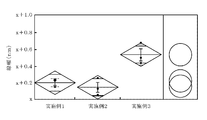
- Example 1 In order to verify the effect of the heat treatment apparatus according to the present disclosure, the heat treatment apparatus 1 shown in the first embodiment is used, and the humidity of the first gas is set to 20%, 50%, and 68%, respectively.
- Examples 1, 2 and 3 were used in which the wafer W was processed in the same manner as in the examples shown in the above embodiment. Each of the examples was repeated three times, and the line width of the resist pattern was measured.
- FIG. 17 shows this result, and the black dots in the figure indicate the measured values of the line width of the resist pattern measured in Examples 1 to 3.
- the rhombus portion in each embodiment is an average rhombus
- the horizontal line in the center is the average value of each of Examples 1 to 3
- the points above and below the rhombus portion are the upper limits of the 95% confidence intervals on both sides of each embodiment. It shows the lower limit.
- the lines drawn at positions separated from the average value of Examples 1 to 3 above and below indicate an overlap mark.
- the bar extending vertically from the average value is the average error bar, and the broken line indicates the standard deviation line.
- a comparison circle of Student's t-test (significant difference 0.05) for each combination.
- Example 3 the line width is significantly thicker than in Examples 1 and 2, and there is a difference of about 0.4 nm in the line width between Examples 1 and 2 and Example 3. Was being done.
- the line width of the resist pattern becomes thicker as the reaction rate increases. Therefore, by setting the humidity of the first gas higher than 60%, the reaction rate can be greatly improved, and the line width can be greatly improved. Can be said to be large.
Landscapes
- Engineering & Computer Science (AREA)
- Physics & Mathematics (AREA)
- General Physics & Mathematics (AREA)
- Microelectronics & Electronic Packaging (AREA)
- Manufacturing & Machinery (AREA)
- Computer Hardware Design (AREA)
- Condensed Matter Physics & Semiconductors (AREA)
- Power Engineering (AREA)
- Chemical & Material Sciences (AREA)
- Organic Chemistry (AREA)
- Optics & Photonics (AREA)
- Exposure Of Semiconductors, Excluding Electron Or Ion Beam Exposure (AREA)
- Photosensitive Polymer And Photoresist Processing (AREA)
Abstract
Description
前記基板を前記ステージに載置される第1の位置と、当該ステージから離れた第2の位置との間で相対的に昇降させる昇降機構と、
前記第1の位置に移動する前の前記第2の位置に位置する前記基板に、前記ステージが設けられる雰囲気よりも湿度が高い第1のガスを供給するガス供給部と、
を備えた。
本開示にかかる熱処理装置1について説明する。この熱処理装置1は、レジスト膜が形成されたウエハWを加熱する装置であり、当該レジスト膜は例えばEUVにより、回路パターンに沿って露光されている。従って、熱処理装置1は、いわゆるポストエクスポージャベーク(PEB)を行う装置である。このレジスト膜を構成するレジストは例えば金属を含有しており、当該金属の一例としてはスズである。レジストについてさらに説明すると、上記のEUVなどの放射線が照射されることでリガンドが金属から脱離し、その状態でレジストが水と反応することで水酸基が導入される。その後に加熱されることで、当該水酸基同士の間で脱水縮合が起こり、その結果、現像液に対して不溶化する。
処理チャンバ20は、天井部を構成する蓋部21と、蓋部21の下方側に位置し底部を含む下側部22と、を備えている。処理チャンバ20の上側部を構成する蓋部21は、支持部29を介してチャンバ用の昇降機構28に接続されている。そして昇降機構28により、蓋部21を下側部22に対して上昇することで、処理チャンバ20が分離して開放されると共に、蓋部21を下降させることで処理チャンバ20が閉鎖される。
その後蓋部21を上昇させて処理チャンバ20を開放すると共に、昇降ピン26を上昇させて、ウエハWをステージ23から上昇させる。そして搬送機構11と昇降ピン26との共働により、ウエハWを搬送機構11に受け渡す。さらにウエハWは、外部の搬送装置に受け渡されて、熱処理装置1から搬出されて、現像処理を受ける。
なお、処理チャンバ20の蓋部21を下降させるタイミングとしては、昇降ピン26の下降と同時であってもよいし、昇降ピン26の下降に遅れても良い。また、処理チャンバ20の排気口としては、ウエハWの中心部上及びウエハWの外周から排気できるように設けることに限られず、いずれか一方のみから排気するようにしてもよい。
続いて第2の実施形態にかかる熱処理装置1Aについて説明する。なおこの熱処理装置1A及び後述の熱処理装置1B、1Cの図面について、第1の実施形態の熱処理装置1と同様の構成の箇所については表示を省略し、処理チャンバ20の部分のみを示している。熱処理装置1Aは、図5に示すように一端がシャワーヘッド30の拡散空間に連通されたガス供給管300の他端側を2本に分岐している。そしてガス供給管300の他端側における一方の端部には、第1のガスを供給する第1のガス供給源301が設置され、他方の端部には、第1のガスよりも湿度が低い第2のガスを供給する第2のガス供給源302が設置されている。第1のガスは、例えば湿度68%の空気であり、第2のガスは、例えば湿度20%の空気である。
また第1のガスよりも湿度の低い第2のガスは、例えば窒素(N2)ガスなどの不活性ガスでもよい。またウエハWに供給するガスの湿度を十分に変化させる観点から、第1のガスと第2のガスとの湿度差は、例えば20%以上であることが好ましい。
またウエハWに供給するガスの湿度をウエハWの面内で調整できるようにしてもよい。図9は、このような熱処理装置1Bに設けられるシャワーヘッド30の一例の下面側平面図である。例えばシャワーヘッド30を下面から見て中央のガス供給領域300Aおよび中央の領域を囲む領域を周方向に4つに分割した各ガス供給領域300B~300Eの5つのガス供給領域300A~300Eを設け、各ガス供給領域300A~300Eにガス吐出孔31を形成する。さらに図10に示すようにシャワーヘッド30内部を各領域に対応させて5つの区画301A~301Eを構成し、各区画301A~301Eに夫々ガス供給管32A~32Eを介してガス供給源33A~33Eを接続する。なお図10では、便宜上5つの区画301A~301Eを横方向に並べて示している。
これによりウエハWの外周側の領域における第1のガスの供給量をウエハWの中心側の領域における第1のガスの供給量よりも多くすることができる。従ってウエハWの外周側の領域の水分量が多くなり、反応速度を高めることができる。これによりウエハWの外周側におけるレジストパターンの線幅の低下を抑制することができる。
本開示にかかる熱処理装置の効果を検証するため、第1の実施形態に示した熱処理装置1を用い、第1のガスの湿度を20%、50%、及び68%に夫々設定して第1の実施形態に示した例と同様にウエハWの処理を行った例を実施例1、2及び3とした。各実施例を夫々3回繰り替えし、レジストパターンの線幅の測定を行った。
3 ガス供給部
23 ステージ
27 昇降機構
W ウエハ
Claims (20)
- 水と反応して加熱されることで露光部または未露光部の現像液に対する溶解性が変化する露光済みのレジスト膜が表面に形成された基板を載置して加熱するステージと、
前記基板を前記ステージに載置される第1の位置と、当該ステージから離れた第2の位置との間で相対的に昇降させる昇降機構と、
前記第1の位置に移動する前の前記第2の位置に位置する前記基板に、前記ステージが設けられる雰囲気よりも湿度が高い第1のガスを供給するガス供給部と、
を備えた熱処理装置。 - 前記ガス供給部は、前記第1の位置の基板に前記第1のガスを供給する請求項1記載の熱処理装置。
- 前記ガス供給部は、前記第1のガスよりも湿度が低い第2のガスを、前記第1の位置または前記第2の位置における前記基板に供給する請求項2記載の熱処理装置。
- 前記ガス供給部は、前記第2のガスを前記第1の位置の基板に供給し、
当該ガス供給部は第1の位置の基板に、前記第1のガス及び前記第2のガスについて順番に供給する請求項3記載の熱処理装置。 - 前記第1のガスについて、前記ガス供給部は、前記基板が前記第2の位置に位置するときには第1の流量で、前記第1の位置に位置するときには、前記第1の流量よりも大きい第2の流量で夫々供給する請求項2に記載の熱処理装置。
- 前記ガス供給部は、
前記第1の位置における前記基板の外周から当該基板の中心部に向けて前記第1のガスを供給する外周ガス供給部と、
前記第1の位置における前記基板に対向する対向部と、
前記対向部から前記基板の表面に前記第1のガスを供給する対向ガス供給部と、を備える請求項2に記載の熱処理装置。 - 前記第1のガスについて、
前記外周ガス供給部からの供給と、前記対向ガス供給部からの供給と、が順番に行われる請求項6記載の熱処理装置。 - 前記ガス供給部は、
前記第1の位置における前記基板に対向する対向部と、
前記基板において互いに異なる第1の領域、第2の領域に独立して前記第1のガスを供給するために、各々吐出孔を備えて前記対向部に設けられる第1のガス供給領域、第2のガス供給領域と、
を備える請求項2に記載の熱処理装置。 - 前記ガス供給部は前記第1のガスとして、前記第1のガス供給領域及び前記第2のガス供給領域から互いに湿度が異なるガスを供給する請求項8記載の熱処理装置。
- 前記ステージを囲むと共に内部が排気され、天井部である前記対向部を含む上側部と、底部を含む下側部とに分離して開放されるチャンバと、
前記基板が前記第1の位置に位置するときに前記チャンバを閉鎖し、前記基板が前記第2の位置に位置するときに前記チャンバを開放するために、前記上側部を下側部に対して相対的に昇降させるチャンバ用の昇降機構と、
を備える請求項6に記載の熱処理装置。 - 前記第1のガスは空気であり、当該第1のガスの湿度は60%より高い請求項1に記載の熱処理装置。
- 前記レジストは金属を含有するレジストである請求項1に記載の熱処理装置。
- 水と反応して加熱されることで露光部または未露光部の現像液に対する溶解性が変化する露光済みのレジストが表面に形成された基板を、前記基板を加熱するステージに載置される第1の位置に位置させる前に、前記第1の位置の上方の第2の位置に位置させる工程と、
次いで前記レジスト膜に水分を供給するためにガス供給部により、前記ステージが設けられる雰囲気よりも湿度が高い第1のガスを前記第2の位置に位置する基板に供給する工程と、
その後基板を第1の位置に移動させて加熱する工程と、
を含む熱処理方法。 - 前記ガス供給部は、前記第1の位置の基板に前記第1のガスを供給する請求項13記載の熱処理方法。
- 前記ガス供給部は、前記第1のガスよりも湿度が低い第2のガスを、前記第1の位置または前記第2の位置における前記基板に供給する請求項14記載の熱処理方法。
- 前記ガス供給部は、前記第1の位置の基板に、前記第1のガス及び前記第2のガスについて順番に供給する請求項15記載の熱処理方法。
- 前記第1のガスについて、前記基板が前記第2の位置に位置するときには第1の流量で、前記第1の位置に位置するときには、前記第1の流量よりも大きい第2の流量で夫々供給する請求項14に記載の熱処理方法。
- 前記第1の位置における前記基板の外周から当該基板の中心部に向けて前記第1のガスを供給する工程と、
前記第1の位置における前記基板に対向する対向部から前記基板の表面に前記第1のガスを供給する工程と、
を含む請求項14に記載の熱処理方法。 - 前記ガス供給部は、前記第1の位置における前記基板に対向する対向部と、
各々吐出孔を備えて前記対向部に設けられる第1のガス供給領域、第2のガス供給領域と、を備え、
第1のガス供給領域、第2のガス供給領域から、前記基板において互いに異なる第1の領域、第2の領域に各々独立して前記第1のガスを供給する工程と、
を備える請求項14に記載の熱処理方法。 - 前記第1の領域、第2の領域に各々独立して前記第1のガスを供給する工程は、前記第1のガス供給領域及び前記第2のガス供給領域から互いに湿度が異なるガスを供給する工程を含む請求項19記載の熱処理方法。
Priority Applications (5)
| Application Number | Priority Date | Filing Date | Title |
|---|---|---|---|
| JP2022509954A JP7456491B2 (ja) | 2020-03-24 | 2021-03-15 | 熱処理装置及び熱処理方法 |
| KR1020227035485A KR20220157990A (ko) | 2020-03-24 | 2021-03-15 | 열처리 장치 및 열처리 방법 |
| US17/906,644 US20230176484A1 (en) | 2020-03-24 | 2021-03-15 | Heat treatment apparatus and heat treatment method |
| CN202180021355.7A CN115280470A (zh) | 2020-03-24 | 2021-03-15 | 热处理装置和热处理方法 |
| JP2024033191A JP2024073500A (ja) | 2020-03-24 | 2024-03-05 | 熱処理方法、プログラム及び熱処理装置 |
Applications Claiming Priority (2)
| Application Number | Priority Date | Filing Date | Title |
|---|---|---|---|
| JP2020-053305 | 2020-03-24 | ||
| JP2020053305 | 2020-03-24 |
Publications (1)
| Publication Number | Publication Date |
|---|---|
| WO2021193202A1 true WO2021193202A1 (ja) | 2021-09-30 |
Family
ID=77892121
Family Applications (1)
| Application Number | Title | Priority Date | Filing Date |
|---|---|---|---|
| PCT/JP2021/010419 WO2021193202A1 (ja) | 2020-03-24 | 2021-03-15 | 熱処理装置及び熱処理方法 |
Country Status (6)
| Country | Link |
|---|---|
| US (1) | US20230176484A1 (ja) |
| JP (2) | JP7456491B2 (ja) |
| KR (1) | KR20220157990A (ja) |
| CN (1) | CN115280470A (ja) |
| TW (1) | TW202147454A (ja) |
| WO (1) | WO2021193202A1 (ja) |
Citations (10)
| Publication number | Priority date | Publication date | Assignee | Title |
|---|---|---|---|---|
| JPH10208997A (ja) * | 1997-01-16 | 1998-08-07 | Fujitsu Ltd | レジスト膜のパターン形成方法及びパターン形成装置 |
| JPH10261558A (ja) * | 1997-01-16 | 1998-09-29 | Tokyo Electron Ltd | 加熱処理装置および加熱処理方法 |
| JPH11190908A (ja) * | 1997-10-03 | 1999-07-13 | Fusion Syst Corp | フォトレジストに形成された像の収縮を減少させるための制御されたアミンポイゾニング |
| JP2008218866A (ja) * | 2007-03-07 | 2008-09-18 | Elpida Memory Inc | パターン形成方法およびパターン形成装置 |
| JP2009294439A (ja) * | 2008-06-05 | 2009-12-17 | Toshiba Corp | レジストパターン形成方法 |
| JP2010135569A (ja) * | 2008-12-04 | 2010-06-17 | Tokyo Electron Ltd | 基板加熱装置及び基板加熱方法 |
| JP2013179354A (ja) * | 2013-06-05 | 2013-09-09 | Tokyo Electron Ltd | 基板処理装置及び基板処理方法 |
| JP2017032658A (ja) * | 2015-07-29 | 2017-02-09 | 信越化学工業株式会社 | レジスト材料並びにこれを用いたパターン形成方法 |
| JP2018107192A (ja) * | 2016-12-22 | 2018-07-05 | 東京エレクトロン株式会社 | 基板処理装置及び基板処理方法 |
| JP2019500490A (ja) * | 2015-10-13 | 2019-01-10 | インプリア・コーポレイションInpria Corporation | 有機スズオキシドヒドロキシドのパターン形成組成物、前駆体およびパターン形成 |
Family Cites Families (9)
| Publication number | Priority date | Publication date | Assignee | Title |
|---|---|---|---|---|
| US6368776B1 (en) * | 1998-03-18 | 2002-04-09 | Tokyo Electron Limited | Treatment apparatus and treatment method |
| JP2001133959A (ja) * | 1999-11-08 | 2001-05-18 | Nikon Corp | マスク基板、パターン保護材、マスク保護装置及びマスク、並びに露光装置及びデバイス製造方法 |
| JP3989221B2 (ja) * | 2001-10-25 | 2007-10-10 | 東京エレクトロン株式会社 | 熱処理装置および熱処理方法 |
| JP2005277268A (ja) * | 2004-03-26 | 2005-10-06 | Dainippon Screen Mfg Co Ltd | 基板処理装置及び基板処理方法 |
| US7465680B2 (en) * | 2005-09-07 | 2008-12-16 | Applied Materials, Inc. | Post deposition plasma treatment to increase tensile stress of HDP-CVD SIO2 |
| US9310684B2 (en) | 2013-08-22 | 2016-04-12 | Inpria Corporation | Organometallic solution based high resolution patterning compositions |
| JP6781031B2 (ja) * | 2016-12-08 | 2020-11-04 | 東京エレクトロン株式会社 | 基板処理方法及び熱処理装置 |
| JP6882091B2 (ja) * | 2017-06-21 | 2021-06-02 | キヤノン株式会社 | 露光装置及び物品の製造方法 |
| JP2019145714A (ja) * | 2018-02-22 | 2019-08-29 | 東芝メモリ株式会社 | パターン形成方法 |
-
2021
- 2021-03-11 TW TW110108619A patent/TW202147454A/zh unknown
- 2021-03-15 US US17/906,644 patent/US20230176484A1/en active Pending
- 2021-03-15 WO PCT/JP2021/010419 patent/WO2021193202A1/ja active Application Filing
- 2021-03-15 CN CN202180021355.7A patent/CN115280470A/zh active Pending
- 2021-03-15 JP JP2022509954A patent/JP7456491B2/ja active Active
- 2021-03-15 KR KR1020227035485A patent/KR20220157990A/ko unknown
-
2024
- 2024-03-05 JP JP2024033191A patent/JP2024073500A/ja active Pending
Patent Citations (10)
| Publication number | Priority date | Publication date | Assignee | Title |
|---|---|---|---|---|
| JPH10208997A (ja) * | 1997-01-16 | 1998-08-07 | Fujitsu Ltd | レジスト膜のパターン形成方法及びパターン形成装置 |
| JPH10261558A (ja) * | 1997-01-16 | 1998-09-29 | Tokyo Electron Ltd | 加熱処理装置および加熱処理方法 |
| JPH11190908A (ja) * | 1997-10-03 | 1999-07-13 | Fusion Syst Corp | フォトレジストに形成された像の収縮を減少させるための制御されたアミンポイゾニング |
| JP2008218866A (ja) * | 2007-03-07 | 2008-09-18 | Elpida Memory Inc | パターン形成方法およびパターン形成装置 |
| JP2009294439A (ja) * | 2008-06-05 | 2009-12-17 | Toshiba Corp | レジストパターン形成方法 |
| JP2010135569A (ja) * | 2008-12-04 | 2010-06-17 | Tokyo Electron Ltd | 基板加熱装置及び基板加熱方法 |
| JP2013179354A (ja) * | 2013-06-05 | 2013-09-09 | Tokyo Electron Ltd | 基板処理装置及び基板処理方法 |
| JP2017032658A (ja) * | 2015-07-29 | 2017-02-09 | 信越化学工業株式会社 | レジスト材料並びにこれを用いたパターン形成方法 |
| JP2019500490A (ja) * | 2015-10-13 | 2019-01-10 | インプリア・コーポレイションInpria Corporation | 有機スズオキシドヒドロキシドのパターン形成組成物、前駆体およびパターン形成 |
| JP2018107192A (ja) * | 2016-12-22 | 2018-07-05 | 東京エレクトロン株式会社 | 基板処理装置及び基板処理方法 |
Also Published As
| Publication number | Publication date |
|---|---|
| CN115280470A (zh) | 2022-11-01 |
| JP2024073500A (ja) | 2024-05-29 |
| KR20220157990A (ko) | 2022-11-29 |
| US20230176484A1 (en) | 2023-06-08 |
| JPWO2021193202A1 (ja) | 2021-09-30 |
| JP7456491B2 (ja) | 2024-03-27 |
| TW202147454A (zh) | 2021-12-16 |
Similar Documents
| Publication | Publication Date | Title |
|---|---|---|
| KR102640367B1 (ko) | 기판 처리 방법 및 열처리 장치 | |
| JP5575706B2 (ja) | 疎水化処理装置、疎水化処理方法、プログラム及びコンピュータ記録媒体。 | |
| US8757089B2 (en) | Coating and developing apparatus, coating and developing method, and storage medium | |
| JP4601080B2 (ja) | 基板処理装置 | |
| JP4952610B2 (ja) | 基板処理装置、基板処理方法並びに記憶媒体 | |
| JP2008177303A (ja) | 基板処理装置、基板処理方法及び記憶媒体 | |
| JP2008060462A (ja) | 塗布処理方法、プログラム、コンピュータ読み取り可能な記録媒体及び塗布処理装置 | |
| JP4967004B2 (ja) | レジスト塗布現像装置およびレジスト塗布現像方法 | |
| JP2009194242A (ja) | 塗布、現像装置、塗布、現像方法及び記憶媒体 | |
| JP2007059633A (ja) | 基板加熱装置及び基板加熱方法 | |
| US8852857B2 (en) | Substrate treatment method | |
| TW201626117A (zh) | 基板處理方法、程式、電腦記憶媒體及基板處理系統 | |
| WO2021193202A1 (ja) | 熱処理装置及び熱処理方法 | |
| US20070003279A1 (en) | Post-exposure baking apparatus and related method | |
| JP5415881B2 (ja) | 疎水化処理装置、疎水化処理方法、プログラム及びコンピュータ記憶媒体 | |
| JP4294893B2 (ja) | 基板熱処理装置及びその整流機構並びに整流方法 | |
| JP5025546B2 (ja) | 基板処理方法及び基板処理装置 | |
| WO2022196336A1 (ja) | 基板処理装置及び基板処理方法 | |
| KR20230167732A (ko) | 열 처리 장치, 열 처리 방법 및 기억 매체 | |
| KR20240048484A (ko) | 기판 처리 방법, 기판 처리 장치 및 컴퓨터 기억 매체 | |
| JP2005166999A (ja) | 基板の処理方法及び基板の露光時の露光量又は焦点位置の変動による基板の処理への影響を低減する方法 | |
| TW202323985A (zh) | 基板處理裝置及基板處理方法 | |
| US8420303B2 (en) | Substrate processing method, computer-readable storage medium and substrate processing system |
Legal Events
| Date | Code | Title | Description |
|---|---|---|---|
| 121 | Ep: the epo has been informed by wipo that ep was designated in this application |
Ref document number: 21774641 Country of ref document: EP Kind code of ref document: A1 |
|
| ENP | Entry into the national phase |
Ref document number: 2022509954 Country of ref document: JP Kind code of ref document: A |
|
| ENP | Entry into the national phase |
Ref document number: 20227035485 Country of ref document: KR Kind code of ref document: A |
|
| NENP | Non-entry into the national phase |
Ref country code: DE |
|
| 122 | Ep: pct application non-entry in european phase |
Ref document number: 21774641 Country of ref document: EP Kind code of ref document: A1 |