WO2021193160A1 - 炭化ケイ素含有膜を形成する方法及び装置 - Google Patents
炭化ケイ素含有膜を形成する方法及び装置 Download PDFInfo
- Publication number
- WO2021193160A1 WO2021193160A1 PCT/JP2021/010183 JP2021010183W WO2021193160A1 WO 2021193160 A1 WO2021193160 A1 WO 2021193160A1 JP 2021010183 W JP2021010183 W JP 2021010183W WO 2021193160 A1 WO2021193160 A1 WO 2021193160A1
- Authority
- WO
- WIPO (PCT)
- Prior art keywords
- gas
- vacuum exhaust
- processing container
- organic compound
- silicon
- Prior art date
- Legal status (The legal status is an assumption and is not a legal conclusion. Google has not performed a legal analysis and makes no representation as to the accuracy of the status listed.)
- Ceased
Links
Images


Classifications
-
- H—ELECTRICITY
- H01—ELECTRIC ELEMENTS
- H01L—SEMICONDUCTOR DEVICES NOT COVERED BY CLASS H10
- H01L21/00—Processes or apparatus adapted for the manufacture or treatment of semiconductor or solid state devices or of parts thereof
- H01L21/02—Manufacture or treatment of semiconductor devices or of parts thereof
- H01L21/02104—Forming layers
- H01L21/02365—Forming inorganic semiconducting materials on a substrate
- H01L21/02518—Deposited layers
- H01L21/02521—Materials
- H01L21/02524—Group 14 semiconducting materials
- H01L21/02529—Silicon carbide
-
- H—ELECTRICITY
- H01—ELECTRIC ELEMENTS
- H01L—SEMICONDUCTOR DEVICES NOT COVERED BY CLASS H10
- H01L21/00—Processes or apparatus adapted for the manufacture or treatment of semiconductor or solid state devices or of parts thereof
- H01L21/02—Manufacture or treatment of semiconductor devices or of parts thereof
- H01L21/02104—Forming layers
- H01L21/02107—Forming insulating materials on a substrate
- H01L21/02225—Forming insulating materials on a substrate characterised by the process for the formation of the insulating layer
- H01L21/0226—Forming insulating materials on a substrate characterised by the process for the formation of the insulating layer formation by a deposition process
- H01L21/02263—Forming insulating materials on a substrate characterised by the process for the formation of the insulating layer formation by a deposition process deposition from the gas or vapour phase
- H01L21/02271—Forming insulating materials on a substrate characterised by the process for the formation of the insulating layer formation by a deposition process deposition from the gas or vapour phase deposition by decomposition or reaction of gaseous or vapour phase compounds, i.e. chemical vapour deposition
- H01L21/0228—Forming insulating materials on a substrate characterised by the process for the formation of the insulating layer formation by a deposition process deposition from the gas or vapour phase deposition by decomposition or reaction of gaseous or vapour phase compounds, i.e. chemical vapour deposition deposition by cyclic CVD, e.g. ALD, ALE, pulsed CVD
-
- C—CHEMISTRY; METALLURGY
- C23—COATING METALLIC MATERIAL; COATING MATERIAL WITH METALLIC MATERIAL; CHEMICAL SURFACE TREATMENT; DIFFUSION TREATMENT OF METALLIC MATERIAL; COATING BY VACUUM EVAPORATION, BY SPUTTERING, BY ION IMPLANTATION OR BY CHEMICAL VAPOUR DEPOSITION, IN GENERAL; INHIBITING CORROSION OF METALLIC MATERIAL OR INCRUSTATION IN GENERAL
- C23C—COATING METALLIC MATERIAL; COATING MATERIAL WITH METALLIC MATERIAL; SURFACE TREATMENT OF METALLIC MATERIAL BY DIFFUSION INTO THE SURFACE, BY CHEMICAL CONVERSION OR SUBSTITUTION; COATING BY VACUUM EVAPORATION, BY SPUTTERING, BY ION IMPLANTATION OR BY CHEMICAL VAPOUR DEPOSITION, IN GENERAL
- C23C16/00—Chemical coating by decomposition of gaseous compounds, without leaving reaction products of surface material in the coating, i.e. chemical vapour deposition [CVD] processes
- C23C16/22—Chemical coating by decomposition of gaseous compounds, without leaving reaction products of surface material in the coating, i.e. chemical vapour deposition [CVD] processes characterised by the deposition of inorganic material, other than metallic material
- C23C16/30—Deposition of compounds, mixtures or solid solutions, e.g. borides, carbides, nitrides
- C23C16/32—Carbides
- C23C16/325—Silicon carbide
-
- C—CHEMISTRY; METALLURGY
- C23—COATING METALLIC MATERIAL; COATING MATERIAL WITH METALLIC MATERIAL; CHEMICAL SURFACE TREATMENT; DIFFUSION TREATMENT OF METALLIC MATERIAL; COATING BY VACUUM EVAPORATION, BY SPUTTERING, BY ION IMPLANTATION OR BY CHEMICAL VAPOUR DEPOSITION, IN GENERAL; INHIBITING CORROSION OF METALLIC MATERIAL OR INCRUSTATION IN GENERAL
- C23C—COATING METALLIC MATERIAL; COATING MATERIAL WITH METALLIC MATERIAL; SURFACE TREATMENT OF METALLIC MATERIAL BY DIFFUSION INTO THE SURFACE, BY CHEMICAL CONVERSION OR SUBSTITUTION; COATING BY VACUUM EVAPORATION, BY SPUTTERING, BY ION IMPLANTATION OR BY CHEMICAL VAPOUR DEPOSITION, IN GENERAL
- C23C16/00—Chemical coating by decomposition of gaseous compounds, without leaving reaction products of surface material in the coating, i.e. chemical vapour deposition [CVD] processes
- C23C16/44—Chemical coating by decomposition of gaseous compounds, without leaving reaction products of surface material in the coating, i.e. chemical vapour deposition [CVD] processes characterised by the method of coating
- C23C16/4412—Details relating to the exhausts, e.g. pumps, filters, scrubbers, particle traps
-
- C—CHEMISTRY; METALLURGY
- C23—COATING METALLIC MATERIAL; COATING MATERIAL WITH METALLIC MATERIAL; CHEMICAL SURFACE TREATMENT; DIFFUSION TREATMENT OF METALLIC MATERIAL; COATING BY VACUUM EVAPORATION, BY SPUTTERING, BY ION IMPLANTATION OR BY CHEMICAL VAPOUR DEPOSITION, IN GENERAL; INHIBITING CORROSION OF METALLIC MATERIAL OR INCRUSTATION IN GENERAL
- C23C—COATING METALLIC MATERIAL; COATING MATERIAL WITH METALLIC MATERIAL; SURFACE TREATMENT OF METALLIC MATERIAL BY DIFFUSION INTO THE SURFACE, BY CHEMICAL CONVERSION OR SUBSTITUTION; COATING BY VACUUM EVAPORATION, BY SPUTTERING, BY ION IMPLANTATION OR BY CHEMICAL VAPOUR DEPOSITION, IN GENERAL
- C23C16/00—Chemical coating by decomposition of gaseous compounds, without leaving reaction products of surface material in the coating, i.e. chemical vapour deposition [CVD] processes
- C23C16/44—Chemical coating by decomposition of gaseous compounds, without leaving reaction products of surface material in the coating, i.e. chemical vapour deposition [CVD] processes characterised by the method of coating
- C23C16/455—Chemical coating by decomposition of gaseous compounds, without leaving reaction products of surface material in the coating, i.e. chemical vapour deposition [CVD] processes characterised by the method of coating characterised by the method used for introducing gases into reaction chamber or for modifying gas flows in reaction chamber
- C23C16/45523—Pulsed gas flow or change of composition over time
- C23C16/45525—Atomic layer deposition [ALD]
- C23C16/45527—Atomic layer deposition [ALD] characterized by the ALD cycle, e.g. different flows or temperatures during half-reactions, unusual pulsing sequence, use of precursor mixtures or auxiliary reactants or activations
-
- C—CHEMISTRY; METALLURGY
- C23—COATING METALLIC MATERIAL; COATING MATERIAL WITH METALLIC MATERIAL; CHEMICAL SURFACE TREATMENT; DIFFUSION TREATMENT OF METALLIC MATERIAL; COATING BY VACUUM EVAPORATION, BY SPUTTERING, BY ION IMPLANTATION OR BY CHEMICAL VAPOUR DEPOSITION, IN GENERAL; INHIBITING CORROSION OF METALLIC MATERIAL OR INCRUSTATION IN GENERAL
- C23C—COATING METALLIC MATERIAL; COATING MATERIAL WITH METALLIC MATERIAL; SURFACE TREATMENT OF METALLIC MATERIAL BY DIFFUSION INTO THE SURFACE, BY CHEMICAL CONVERSION OR SUBSTITUTION; COATING BY VACUUM EVAPORATION, BY SPUTTERING, BY ION IMPLANTATION OR BY CHEMICAL VAPOUR DEPOSITION, IN GENERAL
- C23C16/00—Chemical coating by decomposition of gaseous compounds, without leaving reaction products of surface material in the coating, i.e. chemical vapour deposition [CVD] processes
- C23C16/44—Chemical coating by decomposition of gaseous compounds, without leaving reaction products of surface material in the coating, i.e. chemical vapour deposition [CVD] processes characterised by the method of coating
- C23C16/455—Chemical coating by decomposition of gaseous compounds, without leaving reaction products of surface material in the coating, i.e. chemical vapour deposition [CVD] processes characterised by the method of coating characterised by the method used for introducing gases into reaction chamber or for modifying gas flows in reaction chamber
- C23C16/45523—Pulsed gas flow or change of composition over time
- C23C16/45525—Atomic layer deposition [ALD]
- C23C16/45544—Atomic layer deposition [ALD] characterized by the apparatus
-
- C—CHEMISTRY; METALLURGY
- C23—COATING METALLIC MATERIAL; COATING MATERIAL WITH METALLIC MATERIAL; CHEMICAL SURFACE TREATMENT; DIFFUSION TREATMENT OF METALLIC MATERIAL; COATING BY VACUUM EVAPORATION, BY SPUTTERING, BY ION IMPLANTATION OR BY CHEMICAL VAPOUR DEPOSITION, IN GENERAL; INHIBITING CORROSION OF METALLIC MATERIAL OR INCRUSTATION IN GENERAL
- C23C—COATING METALLIC MATERIAL; COATING MATERIAL WITH METALLIC MATERIAL; SURFACE TREATMENT OF METALLIC MATERIAL BY DIFFUSION INTO THE SURFACE, BY CHEMICAL CONVERSION OR SUBSTITUTION; COATING BY VACUUM EVAPORATION, BY SPUTTERING, BY ION IMPLANTATION OR BY CHEMICAL VAPOUR DEPOSITION, IN GENERAL
- C23C16/00—Chemical coating by decomposition of gaseous compounds, without leaving reaction products of surface material in the coating, i.e. chemical vapour deposition [CVD] processes
- C23C16/44—Chemical coating by decomposition of gaseous compounds, without leaving reaction products of surface material in the coating, i.e. chemical vapour deposition [CVD] processes characterised by the method of coating
- C23C16/455—Chemical coating by decomposition of gaseous compounds, without leaving reaction products of surface material in the coating, i.e. chemical vapour deposition [CVD] processes characterised by the method of coating characterised by the method used for introducing gases into reaction chamber or for modifying gas flows in reaction chamber
- C23C16/45523—Pulsed gas flow or change of composition over time
- C23C16/45525—Atomic layer deposition [ALD]
- C23C16/45553—Atomic layer deposition [ALD] characterized by the use of precursors specially adapted for ALD
-
- C—CHEMISTRY; METALLURGY
- C23—COATING METALLIC MATERIAL; COATING MATERIAL WITH METALLIC MATERIAL; CHEMICAL SURFACE TREATMENT; DIFFUSION TREATMENT OF METALLIC MATERIAL; COATING BY VACUUM EVAPORATION, BY SPUTTERING, BY ION IMPLANTATION OR BY CHEMICAL VAPOUR DEPOSITION, IN GENERAL; INHIBITING CORROSION OF METALLIC MATERIAL OR INCRUSTATION IN GENERAL
- C23C—COATING METALLIC MATERIAL; COATING MATERIAL WITH METALLIC MATERIAL; SURFACE TREATMENT OF METALLIC MATERIAL BY DIFFUSION INTO THE SURFACE, BY CHEMICAL CONVERSION OR SUBSTITUTION; COATING BY VACUUM EVAPORATION, BY SPUTTERING, BY ION IMPLANTATION OR BY CHEMICAL VAPOUR DEPOSITION, IN GENERAL
- C23C16/00—Chemical coating by decomposition of gaseous compounds, without leaving reaction products of surface material in the coating, i.e. chemical vapour deposition [CVD] processes
- C23C16/44—Chemical coating by decomposition of gaseous compounds, without leaving reaction products of surface material in the coating, i.e. chemical vapour deposition [CVD] processes characterised by the method of coating
- C23C16/455—Chemical coating by decomposition of gaseous compounds, without leaving reaction products of surface material in the coating, i.e. chemical vapour deposition [CVD] processes characterised by the method of coating characterised by the method used for introducing gases into reaction chamber or for modifying gas flows in reaction chamber
- C23C16/45557—Pulsed pressure or control pressure
-
- H—ELECTRICITY
- H01—ELECTRIC ELEMENTS
- H01L—SEMICONDUCTOR DEVICES NOT COVERED BY CLASS H10
- H01L21/00—Processes or apparatus adapted for the manufacture or treatment of semiconductor or solid state devices or of parts thereof
- H01L21/02—Manufacture or treatment of semiconductor devices or of parts thereof
- H01L21/02104—Forming layers
- H01L21/02107—Forming insulating materials on a substrate
- H01L21/02109—Forming insulating materials on a substrate characterised by the type of layer, e.g. type of material, porous/non-porous, pre-cursors, mixtures or laminates
- H01L21/02112—Forming insulating materials on a substrate characterised by the type of layer, e.g. type of material, porous/non-porous, pre-cursors, mixtures or laminates characterised by the material of the layer
- H01L21/02123—Forming insulating materials on a substrate characterised by the type of layer, e.g. type of material, porous/non-porous, pre-cursors, mixtures or laminates characterised by the material of the layer the material containing silicon
- H01L21/02167—Forming insulating materials on a substrate characterised by the type of layer, e.g. type of material, porous/non-porous, pre-cursors, mixtures or laminates characterised by the material of the layer the material containing silicon the material being a silicon carbide not containing oxygen, e.g. SiC, SiC:H or silicon carbonitrides
-
- H—ELECTRICITY
- H01—ELECTRIC ELEMENTS
- H01L—SEMICONDUCTOR DEVICES NOT COVERED BY CLASS H10
- H01L21/00—Processes or apparatus adapted for the manufacture or treatment of semiconductor or solid state devices or of parts thereof
- H01L21/02—Manufacture or treatment of semiconductor devices or of parts thereof
- H01L21/02104—Forming layers
- H01L21/02107—Forming insulating materials on a substrate
- H01L21/02109—Forming insulating materials on a substrate characterised by the type of layer, e.g. type of material, porous/non-porous, pre-cursors, mixtures or laminates
- H01L21/02205—Forming insulating materials on a substrate characterised by the type of layer, e.g. type of material, porous/non-porous, pre-cursors, mixtures or laminates the layer being characterised by the precursor material for deposition
- H01L21/02208—Forming insulating materials on a substrate characterised by the type of layer, e.g. type of material, porous/non-porous, pre-cursors, mixtures or laminates the layer being characterised by the precursor material for deposition the precursor containing a compound comprising Si
- H01L21/02211—Forming insulating materials on a substrate characterised by the type of layer, e.g. type of material, porous/non-porous, pre-cursors, mixtures or laminates the layer being characterised by the precursor material for deposition the precursor containing a compound comprising Si the compound being a silane, e.g. disilane, methylsilane or chlorosilane
-
- H—ELECTRICITY
- H01—ELECTRIC ELEMENTS
- H01L—SEMICONDUCTOR DEVICES NOT COVERED BY CLASS H10
- H01L21/00—Processes or apparatus adapted for the manufacture or treatment of semiconductor or solid state devices or of parts thereof
- H01L21/02—Manufacture or treatment of semiconductor devices or of parts thereof
- H01L21/02104—Forming layers
- H01L21/02365—Forming inorganic semiconducting materials on a substrate
- H01L21/02612—Formation types
- H01L21/02617—Deposition types
- H01L21/0262—Reduction or decomposition of gaseous compounds, e.g. CVD
-
- H—ELECTRICITY
- H01—ELECTRIC ELEMENTS
- H01L—SEMICONDUCTOR DEVICES NOT COVERED BY CLASS H10
- H01L21/00—Processes or apparatus adapted for the manufacture or treatment of semiconductor or solid state devices or of parts thereof
- H01L21/02—Manufacture or treatment of semiconductor devices or of parts thereof
- H01L21/027—Making masks on semiconductor bodies for further photolithographic processing not provided for in group H01L21/18 or H01L21/34
- H01L21/033—Making masks on semiconductor bodies for further photolithographic processing not provided for in group H01L21/18 or H01L21/34 comprising inorganic layers
- H01L21/0332—Making masks on semiconductor bodies for further photolithographic processing not provided for in group H01L21/18 or H01L21/34 comprising inorganic layers characterised by their composition, e.g. multilayer masks, materials
Definitions
- the present disclosure relates to a method and an apparatus for forming a silicon carbide-containing film.
- SiC film a film forming technique for a silicon carbide-containing film
- Patent Document 1 describes a method of alternately supplying acetylene gas and dichlorosilane gas into a reaction tube to obtain a SiC film at a high temperature of 900 ° C. to 1100 ° C.
- Patent Document 2 describes a method of forming a SiC film by simultaneously supplying triethylamine gas and disilane gas into a treatment chamber. In this method, the pressure adjustment valve is closed after the simultaneous supply of both gases, and the triethylamine gas and the disilane gas are confined in the treatment chamber to improve the gas phase reaction efficiency.
- the present disclosure provides a technique capable of forming a silicon carbide-containing film having good film quality and improving the film formation rate.
- the present disclosure is a method of forming a silicon carbide-containing film on a substrate in a processing container in which vacuum exhaust is performed.
- a step of supplying the gas of the silicon precursor containing the silicon compound to the processing container after the gas of the carbon precursor is supplied and reacting the organic compound adsorbed on the substrate with the silicon compound is included.
- the step of adsorbing the organic compound on the substrate and the step of reacting the organic compound with the silicon compound are alternately repeated a plurality of times to form the silicon carbide-containing film.
- the vacuum exhaust is restricted, the gas of the carbon precursor is retained in the processing container, the restriction of the vacuum exhaust is released, and the gas stays in the processing container. Ejecting carbon precursor gas and During the step of reacting the organic compound adsorbed on the substrate with the silicon compound, the supply of the silicon precursor gas to the processing container is stopped, and after the supply is stopped, the vacuum exhaust is not restricted. It has that.
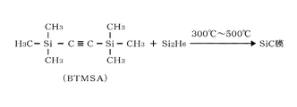
- This is an example of a chemical reaction formula used in the film forming method of the present disclosure.
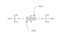
- This is an example of a reaction model related to the chemical reaction formula.
- It is a time chart which shows an example of the film forming method.
- It is a time chart which shows another example of a film forming method.
- It is a structural formula showing another example of a carbon precursor.
- This is an example of a reaction model related to the other chemical reaction formula.
- It is explanatory drawing which shows the variation of a carbon precursor.
- It is explanatory drawing which shows the variation of a silicon precursor.
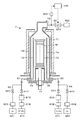
- the film forming apparatus 1 includes a processing container 10 for accommodating a substrate, for example, a semiconductor wafer (hereinafter referred to as “wafer”) W, and the processing container 10 is formed of a metal such as aluminum (Al) in a substantially cylindrical shape.
- a carry-in outlet 11 for carrying in or out the wafer W is formed by a gate valve 12 so as to be openable and closable.
- the exhaust duct 13 is provided with a slit 131 along the inner peripheral surface, and an exhaust port 132 is formed on the outer wall of the exhaust duct 13.
- a top wall 14 is provided on the upper surface of the exhaust duct 13 so as to close the upper opening of the processing container 10 via the insulating member 15, and the exhaust duct 13 and the insulating member 15 are hermetically sealed with a seal ring 16. It will be stopped.
- a mounting table 2 for horizontally supporting the wafer W is provided inside the processing container 10, and the mounting table 2 is made of a ceramic material such as aluminum nitride (AlN) or a metal material such as aluminum or nickel alloy. It is formed in a disk shape.
- a heater 21 forming a heating portion for heating the wafer W is embedded in the mounting table 2, and the outer peripheral region and the side surface of the upper surface of the mounting table 2 are covered members 23 made of ceramics such as alumina. Covered by.
- the mounting table 2 is connected to an elevating mechanism 25 provided below the processing container 10 via a support member 24, and transfers the processing position shown by the solid line in FIG. 1 and the wafer W shown by the alternate long and short dash line below the processing position. It is configured to be able to move up and down with and from the position.
- reference numeral 17 indicates a partition member for vertically partitioning the inside of the processing container 10 when the mounting table 2 is raised to the processing position.
- Three support pins 26 (only two of which are shown) are vertically provided on the lower side of the mounting table 2 in the processing container 10 by an elevating mechanism 27 provided below the processing container 10.
- the support pin 26 is inserted through a through hole 22 of the mounting table 2 at the delivery position so as to be recessable with respect to the upper surface of the mounting table 2, and the external transport mechanism (not shown) and the mounting table 2 are connected to each other. It is used for the transfer of wafers W between.
- Reference numerals 28 and 29 in the drawing refer to bellows that separate the atmosphere inside the processing container 10 from the outside air and expand and contract as the mounting table 2 and the support pin 26 move up and down, respectively.
- the processing container 10 is provided with a shower head 3 for supplying the processing gas in a shower shape in the processing container 10 so as to face the mounting table 2.
- the shower head 3 includes a main body 31 fixed to the top wall 14 of the processing container 10 and a shower plate 32 connected under the main body 31, and the inside thereof forms a gas diffusion space 33. ..
- An annular protrusion 34 projecting downward is formed on the peripheral edge of the shower plate 32, and a gas discharge hole 35 is formed on the flat surface inside the annular protrusion 34.
- the gas supply system 5 is connected to the gas diffusion space 33 via the gas introduction hole 36.
- the gas supply system 5 includes a carbon precursor supply unit configured to supply the carbon precursor gas to the processing container 10 and a silicon precursor supply unit configured to supply the silicon precursor gas. ..
- the carbon precursor supply unit includes a carbon precursor gas supply source 51 and a gas supply path 511, and the gas supply path 511 is provided with a flow rate adjusting unit 512, a storage tank 513, and a valve 514 from the upstream side. NS.
- the carbon precursor contains an organic compound having an unsaturated carbon bond, and for example, bistrimethylsilylacetylene (BTMSA) having a triple bond is used.
- BTMSA bistrimethylsilylacetylene
- the carbon precursor gas supplied from the supply source 51 is temporarily stored in the storage tank 513, boosted to a predetermined pressure in the storage tank 513, and then supplied into the processing container 10.
- BTMSA is a liquid at room temperature, and the gas obtained by heating is supplied to the storage tank 513 and stored.
- the supply and stop of the carbon precursor gas from the storage tank 513 to the processing container 10 is performed by opening and closing the valve 514.
- the silicon precursor supply unit includes a gas supply source 52 and a gas supply path 521 of the silicon precursor, and the gas supply path 521 is provided with a flow rate adjusting unit 522, a storage tank 523, and a valve 524 from the upstream side.
- the silicon precursor contains a silicon compound, and for example, disilane (Si 2 H 6 ) is used.
- the gas of silicon precursor may be referred to as silicon precursor gas or disilane gas.
- the silicon precursor gas supplied from the supply source 52 is temporarily stored in the storage tank 523, boosted to a predetermined pressure in the storage tank 523, and then supplied into the processing container 10.
- the supply and stop of the silicon precursor gas from the storage tank 523 to the processing container 10 is performed by opening and closing the valve 524.
- the gas supply system 5 includes supply sources 53 and 54 of an inert gas such as argon (Ar) gas.
- the Ar gas supplied from one of the supply sources 53 is used as a purge gas for carbon precursor gas.
- the supply source 53 is connected from the upstream side to the downstream side of the valve 514 in the gas supply path 511 of the carbon precursor gas via the gas supply path 531 provided with the flow rate adjusting unit 532 and the valve 533.
- the Ar gas supplied from the other supply source 54 is used as a purge gas for silicon precursor gas.
- the supply source 54 is connected from the upstream side to the downstream side of the valve 524 in the gas supply path 521 of the silicon precursor gas via the gas supply path 541 provided with the flow rate adjusting unit 542 and the valve 543.
- the supply and stop of Ar gas to the processing container 10 is performed by opening and closing valves 533 and 543.
- the processing container 10 is connected to a vacuum exhaust passage 62 via an exhaust port 132, and a vacuum pump configured to execute vacuum exhaust of the gas in the processing container 10 on the downstream side of the vacuum exhaust passage 62, for example.
- a vacuum exhaust unit 61 is provided in the vacuum exhaust passage 62.
- an APC (Auto pressure Controller) valve 63 is interposed between the processing container 10 and the vacuum exhaust portion 61 as a pressure control valve.
- the pressure inside the processing container 10 is adjusted by a pressure adjusting mechanism.
- the pressure adjusting mechanism of this example includes a vacuum exhaust section 61, a vacuum exhaust passage 62, and an APC valve (pressure adjusting valve) 63.
- the APC valve 63 is composed of, for example, a butterfly valve, and is provided with a vacuum exhaust passage 62 that can be opened and closed, and has a role of adjusting the pressure in the processing container 10 by increasing or decreasing the conductance of the vacuum exhaust passage 62 by adjusting the opening degree thereof. Fulfill.
- the APC valve 63 is opened and closed to adjust the pressure in the processing container 10, and by reducing the opening degree, the exhaust in the processing container 10 is hindered and the exhaust flow rate decreases. .. Further, in the vacuum exhaust passage 62, for example, a pressure detection unit 64 is provided between the exhaust port 132 and the APC valve 63. The pressure detection unit 64 is provided in the immediate vicinity of the exhaust port 132, and the pressure detection value can be regarded as the pressure detection value in the processing container 10.
- the APC valve 63 in this example has a pressure adjusting function and an opening degree setting function.
- the pressure adjusting function is a function of controlling the pressure by adjusting the opening degree based on the pressure detected value by the pressure detecting unit 64 and the preset pressure target value.
- the opening degree setting function is a function of fixing the opening degree of the valve body to a preset opening degree. Then, in the film formation process of the SiC film described later, the pressure adjusting function and the opening degree setting function are switched based on the command from the control unit 100.
- the control unit 100 is composed of, for example, a computer, and includes a data processing unit including a program, a memory, and a CPU.
- a control signal is sent from the control unit 100 to each part of the film forming apparatus 1, and a command (each step) is incorporated so as to proceed with the film forming process of the SiC film described later.
- the program is stored in a storage unit such as a computer storage medium such as a flexible disk, a compact disk, a hard disk, or an MO (magneto-optical disk) and installed in the control unit 100.
- control unit 100 is configured to control the film forming process for forming the SiC film on the wafer W.
- a suction step of supplying BTMSA gas as a carbon precursor to adsorb BTMSA on the wafer W is performed.
- a reaction step is carried out in which disilane gas is supplied as a silicon precursor to react BTMSA adsorbed on the wafer W with disilane.
- the adsorption step and the reaction step are alternately repeated a plurality of times to control the formation of a SiC film by the ALD (Atomic layer deposition) method.
- ALD Atomic layer deposition
- control unit 100 is configured to control the vacuum exhaust by the vacuum exhaust unit 61 in the suction step and temporarily limit the vacuum exhaust in the processing container 10. In this vacuum exhaust control, after the carbon precursor gas is retained in the processing container 10, the restriction on the vacuum exhaust is released, and the control is performed so that the carbon precursor gas in the processing container 10 is discharged.
- control unit 100 starts limiting the vacuum exhaust during the period of supplying the carbon precursor gas to the processing container 10, and after a predetermined time has elapsed from the stop of the supply of the gas, the limitation is described. Is configured to control the termination of. Furthermore, during the reaction step, the supply of silicon precursor gas to the processing container 10 is stopped, and after the supply is stopped, the vacuum exhaust unit 61 executes control to continue vacuum exhaust so as not to limit the vacuum exhaust. It is configured to do.
- the film formation method of the present disclosure uses a carbon precursor gas and a silicon precursor gas, and forms a SiC film by a thermal reaction of 500 ° C. or lower without using plasma by the ALD method. It is a thing.
- FIG. 2 shows an example in which BTMSA having a triple bond, which is a carbon precursor, and disilane, which is a silicon precursor, are thermally reacted at a temperature in the range of, for example, 300 ° C. or higher and 500 ° C. or lower.
- reaction model 1 The mechanism by which a SiC film can be formed by such a thermal reaction at a low temperature will be considered using the reaction model 1 shown in FIG.
- Disilane is thermally decomposed by heating at around 400 ° C. to generate a SiH 2 radical having an unpaired electron in the Si atom, and this SiH 2 radical has an empty p-orbital.
- this empty p-orbital acts as an electrophile that attacks the ⁇ bond of the unsaturated carbon bond of BTMSA, which is rich in electrons, and acts on the triple bond of BTMSA.
- C forming the triple bond reacts with Si of the SiH 2 radical to form a SiC bond.
- the reaction model 1 is for inferring the reason why the SiC film can be formed at a low temperature, which has been considered difficult in the past, and does not limit the actual reaction route. If the SiC film can be formed at a temperature of 500 ° C. or lower without using plasma, the SiC film may be formed via another reaction path.
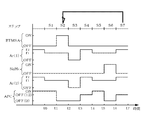
- FIGS. 4A and 4B show the timing of starting and stopping the supply of BTMSA gas, Ar gas, and disilane gas, and the timing of opening and closing the APC valve 63, respectively.
- BTMSA gas and disilane gas "ON" on the vertical axis indicates a supply state, and "OFF" indicates a supply stop state, respectively.
- Ar (1) shown in FIGS. 4A and 4B refers to Ar gas for purging BTMSA gas
- Ar (2) in FIG. 4B refers to Ar gas for purging disilane gas, respectively.
- "ON” of the APC valve 63 means that the pressure adjusting function of the APC valve 63 is set to “ON” and the opening degree is adjusted so as to approach the pressure target value based on the pressure detection value.
- "OFF” of the APC valve 63 means that the pressure adjusting function is set to “OFF” and the opening degree of the APC valve 63 is adjusted to the set opening degree by the opening degree setting function.
- “OFF (0)” means that the opening degree is set to 0%, that is, the fully closed state
- “OFF (12)” means that the opening degree is set to 12%.
- the film forming process will be described with reference to FIG. 4A.
- a step of carrying the wafer W into the processing container 10, closing the gate valve 12 of the processing container 10, and accommodating the wafer W in the processing container 10 is performed.
- the heating of the wafer W by the heater 21 is started, and the vacuum exhaust unit 61 performs vacuum exhaust in the processing container 10.
- the APC valve 63 sets the pressure adjusting function to "ON”, performs opening / closing control based on the pressure detection value from the pressure detection unit 64, and controls the inside of the processing container 10 to a pressure target value of, for example, 1000 Pa.
- Ar (1) and (2) which are purge gases, are supplied into the processing container 10 at a first flow rate r1 such as 50 sccm, respectively, and the first pressure adjustment step S1 is executed.
- Ar (1) and (2) are introduced into the processing container 10 via the shower head 3 and flow toward the exhaust port 132 on the side of the wafer W placed on the mounting table 2 at the processing position. , Is discharged from the processing container 10 via the vacuum exhaust passage 62.
- the valve 514 is opened to start supplying the gas of BTMSA, which is a carbon precursor, to the processing container 10, and the adsorption step of adsorbing BTMSA on the wafer W is started.
- BTMSA gas stored in the storage tank 513
- the BTMSA supply step S2 is carried out.
- Ar (1) and Ar (2) continue to be supplied at the first flow rate r1.
- the valve 514 is closed to stop the supply of BTMSA, and the BTMSA filling step S3 is performed.
- the supply of Ar (1) and Ar (2) is stopped.
- the adsorption step comprises a BTMSA supply step S2 and a BTMSA encapsulation step S3.
- the heater 21 heats the wafer W to a temperature in the range of 300 ° C. or higher and 500 ° C. or lower, for example, 410 ° C. ..
- the BTMSA encapsulation step S3 is provided after the BTMSA supply step S2, and the BTMSA gas is retained in the processing container 10 by temporarily limiting the vacuum exhaust in the processing container 10 during these periods.
- the control of the APC valve 63 is switched to the opening degree setting function, and the opening degree is set to "0%", that is, in the fully closed state.
- the exhaust gas in the processing container 10 is temporarily substantially stopped during the period of the BTMSA supply step S2 and the BTMSA filling step S3. Therefore, by performing the above operation, it is possible to maintain a state in which the BTMSA gas is filled and stays in the processing space formed between the shower head 3 and the mounting table 2.
- the APC valve 63 does not have a function of separating the upstream side and the downstream side thereof, and even if the APC valve 63 is set to the fully closed state, gas may continue to be discharged from the processing container 10 although the amount is small. Even in such a case, it has been confirmed that the effect of retaining BTMSA gas in the processing container 10 can be obtained as compared with the case where the APC valve 63 is in the open state.
- the residence time of BTMSA gas in the processing container 10 is extended as compared with the case where vacuum exhaust is continued, and the time for contacting BTMSA gas with the wafer W can be lengthened.
- the time required for the chemical adsorption can be sufficiently secured, so that a sufficient amount of BTMSA is applied to the surface of the wafer W. Can be adsorbed.
- the temporary restriction of the vacuum exhaust in the processing container 10 is implemented by making the opening degree of the APC valve 63 smaller than before the restriction is started. Therefore, not only the case where the APC valve 63 is fully closed as in the above-mentioned example, but also the case where the opening degree of the APC valve 63 is made smaller than before the restriction is started is included. If the opening degree of the APC valve 63 is made smaller than that before the start of the limitation, the exhaust of the carbon precursor gas in the processing container 10 is suppressed and the exhaust flow rate is lowered, so that the gas stays in the processing container 10. .. Therefore, depending on the type of gas of the carbon precursor and the film quality of the target SiC film, the organic compound in the gas may be sufficiently adsorbed on the wafer W even if the APC valve 63 is not fully closed. May be possible.
- the opening degree of the APC valve 63 is set to, for example, 12%, and Ar (1) and (2) are supplied at a second flow rate r2, for example, 500 sccm, respectively, and the first purge step is performed.
- the opening degree of the APC valve 63 is fixed at 12% to promote forced exhaust in the processing container 10.
- step S5 the opening degree of the APC valve 63 is adjusted based on the pressure detection value so that the inside of the processing container 10 approaches the pressure target value.
- the second pressure adjustment step in step S5 may be omitted in order to improve throughput and the like.
- the adsorption step is from time t1 to time t3 when the Ar gas purge is started. Then, the temporary restriction of the vacuum exhaust starts at time t1 during the period of supplying the BTMSA gas to the processing container 10 and ends at t3 after the elapse of the preset time. Therefore, the period after the supply of BTMSA gas is stopped at time t2 is also included in the period in which the vacuum exhaust is restricted.
- the time t3 is appropriately set depending on the type of gas of the carbon precursor, the target film quality of the SiC film, and the like. As an example, the supply time of BTMSA gas is 1 second, and the time for temporarily limiting the vacuum exhaust is 3 seconds or more, preferably 10 seconds or more.
- the pressure inside the processing container 10 fluctuates by temporarily limiting the vacuum exhaust of the processing container 10, but as described above, the BTMSA gas supply time and the vacuum exhaust are temporarily limited. The time to do is short. Therefore, the amount of pressure fluctuation in the processing container 10 is not so large, and there is no great influence that deteriorates the film quality of the formed SiC film.
- the valve 524 is opened to start the supply of disilane gas, which is a silicon precursor, and the disilane supply step S6 is carried out.
- This step S6 is a reaction step of reacting BTMSA adsorbed on the wafer W with disilane.
- the disilane gas is supplied for a relatively short time, for example, 1 second, until the valve 524 is closed and the supply is stopped at time t6.
- the disilane gas stored in the storage tank 523 is supplied into the processing container 10 in a short time.
- Ar (1) and Ar (2) are supplied at the first flow rate r1.
- the disilane gas is retained in the processing container 10 by temporarily limiting the vacuum exhaust in the processing container 10.
- the control of the APC valve 63 is switched to the opening setting function, and the opening is set to "0%", that is, in the fully closed state. That is, the exhaust gas in the processing container 10 is temporarily and substantially stopped for a relatively short time until the supply of the disilane gas is started at the time t5 and the supply is stopped at the time t6. Therefore, by performing the above operation, the processing space formed between the shower head 3 and the mounting table 2 is in contact with the BTMSA adsorbed on the wafer W in a state of being filled with disilane gas and reacts. Form SiC.
- the opening degree of the APC valve 63 is set to, for example, 12%, Ar (1) and (2) are supplied at the second flow rate r2, respectively, and the second purge step S7 is performed. do.
- the forced exhaust in the processing container 10 is advanced by fixing the opening degree of the APC valve 63 to 12%. As a result, the excess disilane gas and Ar gas in the processing container 10 are quickly discharged from the processing container 10. After that, steps 2 to 7 are repeated again.
- the vacuum exhaust of the processing container 10 may be controlled to be continued without temporarily limiting the vacuum exhaust. Since the time chart of FIG. 4B is the same as that of FIG. 4A except for the control of the APC valve 63 in the disilane supply step S6, the description other than the APC valve 63 of the step S6 will be omitted.
- the APC valve 63 switches the pressure adjustment function to “ON” at the time t4 when the second pressure adjustment step S5 is started, and the processing container is also based on the pressure detection value in the disilane gas supply step S6. The opening degree is adjusted so that the inside of 10 approaches the pressure target value.
- the disilane gas introduced from the shower head 3 flows through the processing container 10 toward the exhaust port 132 and reacts with the BTMSA adsorbed on the wafer W to form SiC.
- amorphous Si When the excess disilane gas is decomposed on the surface of the wafer W, amorphous Si may be deposited and an amorphous Si film may be formed. Therefore, as shown in FIG. 4A, the purging is performed immediately after the supply of the disilane gas is stopped, or as shown in FIG. 4B, the vacuum exhaust in the processing container 10 is continued during the supply period of the disilane gas. In other words, in the disilane gas, the formation of the amorphous Si film can be suppressed by not providing the encapsulation step like BTMSA and not limiting the vacuum exhaust after the supply of the disilane gas is stopped.
- the gas supply of BTMSA which is the carbon precursor of step S2
- the step of adsorbing BTMSA on the wafer W and the step of reacting BTMSA with disilane are alternately performed by the method described above.
- the SiC film thus formed by the ALD method is surely formed with a SiC bond.
- XPS X-ray Photoelectron Spectroscopy
- the vacuum exhaust in the processing container 10 is restricted and the BTMSA gas stays in the processing container 10. I'm letting you. Therefore, as described above, the chemical adsorption of BTMSA on the wafer surface is promoted, a SiC film having good film quality can be formed, and the film formation rate can be improved.
- a SiC film having a good film quality is a film having a good ratio (Si / C ratio) of a silicon (Si) component and a carbon (C) component in the SiC film, and specifically, the Si / C ratio is 1. It is a film close to. From the examples described later, it is recognized that the carbon atom (C) having a SiC bond in the SiC film is increased by the method of the present disclosure.
- the vacuum exhaust in the processing container 10 is not restricted at least after the supply of disilane gas is stopped (steps 4A and 4B). S7). Therefore, excess disilane gas not used for the reaction with BTMSA is rapidly discharged from the processing container 10, and the formation of the above-mentioned amorphous Si film is suppressed. Therefore, from this point as well, the increase of the Si component in the SiC film can be suppressed, the formation of the amorphous Si film can be suppressed, and a film having a good Si / C ratio can be formed.
- a silicon precursor for example, disilane gas
- the SiC film formed by thermally reacting the carbon precursor and the silicon precursor at a relatively low temperature of 300 ° C. or higher and 500 ° C. or lower using the ALD method is of high quality, and is a hard mask material, an insulating film, or the like. It has properties suitable for a low dielectric constant film.
- the allowable temperature during the film forming process is 500 ° C. or less in order to suppress the diffusion of metal from the metal wiring layer. On the other hand, even if it is possible to form a film at a low temperature of 400 ° C.
- the method of forming a SiC film using plasma causes great damage to other films and wiring layers constituting the semiconductor element due to plasma. Therefore, it may be a problem. Therefore, it is effective that the SiC film can be formed at a temperature of 500 ° C. or lower without using plasma by the film forming method of the present disclosure, which leads to the expansion of applications of the SiC film.
- BTMSA has less intramolecular polarization (localization of electric charge) and is less likely to be chemically adsorbed to the surface of the wafer W than a molecule having a large amount of polarization. Therefore, in a method such as the ALD method in which the supply of BTMSA gas is repeated for a short time, if vacuum exhaust is performed in the adsorption step, BTMSA may be discharged from the processing container 10 before being sufficiently chemically adsorbed. .. As a result, there are problems that the C component in the SiC film is reduced, the desired SiC film having a Si / C ratio cannot be formed, and the film formation rate is low.
- the limitation of the vacuum exhaust in the processing container 10 is implemented by reducing the opening degree of the APC valve 63, so that it is easy to control. Furthermore, when BTMSA is used as the carbon precursor, BTMSA does not form a thermal decomposition film by itself, so that there is an advantage that a SiC film can be easily formed by the ALD method.
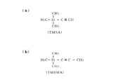
- the carbon precursor shown in FIG. 5 (a) is trimethylsilylacetylene (TMSA) having a triple bond.
- the carbon precursor shown in FIG. 5B is trimethylsilylmethylacetylene (TMSMA) having a triple bond.
- TMSA trimethylsilylacetylene
- TMSMA trimethylsilylmethylacetylene
- a SiC film can also be formed by thermally reacting these TMSA gas and TMSMA gas with a silicon precursor, for example, disilane gas, at a temperature in the range of 300 ° C. or higher and 500 ° C. or lower.
- TMSA and TMSMA also have less intramolecular polarization and are less likely to cause chemisorption on the wafer surface, but chemical adsorption with the wafer can be promoted by temporarily limiting vacuum exhaust in the adsorption step.
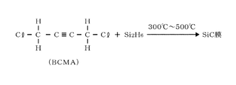
- the carbon precursor shown in FIG. 6 is bischloromethylacetylene (BCMA) having a triple bond which is an unsaturated carbon bond and containing a halogen.
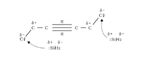
- FIG. 6 shows an example in which a BCMA gas and a silicon precursor, for example, disilane gas, are thermally reacted at a temperature in the range of 300 ° C. or higher and 500 ° C. or lower. Regarding this thermal reaction, it is presumed that the reaction model 1 shown in FIG. 3 and the reaction model 2 shown in FIG. 7 proceed at the same time.
- the reaction model 2 has nucleophilicity in which BCMA is polarized by having a halogen group (Cl group) and the positive polarization site ( ⁇ +) of the SiH 2 radical attacks the negative polarization site ( ⁇ ). In this way, the SiH 2 radical reacts with C at the molecular end where Cl is bonded to form a SiC bond.
- the carbon precursor containing an organic compound having an unsaturated carbon bond is not limited to the above-mentioned BTMSA, TMSA, TMSMA and BCMA. If the thermal reaction with the silicon precursor proceeds at a temperature of 500 ° C. or lower and it is possible to form a SiC film, another carbon precursor may be used.
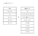
- the carbon precursor a combination of a skeleton and a side chain shown in FIG. 8 can be used.
- the skeleton of the carbon precursor is an unsaturated bond portion of an organic compound, and can exemplify the unsaturated carbon bond of a triple bond or a double bond of C.
- the side chain of the carbon precursor is the part that is attached to the skeleton.
- the side chain that binds to one C is X
- the side chain that binds to the other C is Y.
- These side chains X and Y may be the same as each other or may be different from each other.
- Side chains include hydrogen (H) atoms, halogens, alkyl groups with a C number of 5 or less, triple bonds of C, double bonds of C, Si (Z), C (Z), N (Z), O. (Z) and the like can be mentioned.
- Si (Z), C (Z), N (Z), and O (Z) are the sites where the skeleton is bonded to C, which is Si, C, N. , O, and (Z) indicates an arbitrary atomic group.
- the silicon precursor a combination of a skeleton and a side chain shown in FIG. 9 can be used.
- the skeleton of the silicon precursor is a Si—Si bond in terms of disilane.
- the side chain of the silicon precursor is the part that is attached to the skeleton. Assuming that the skeleton is Si—Si, the side chain X that binds to one Si and the side chain Y that binds to the other Si may be the same or different from each other. Examples of the skeleton include Si—Si, Si, Si—C, Si—N, Si—O and the like.
- Side chains include hydrogen atoms, halogens, alkyl groups with a C number of 5 or less, triple bonds of C, double bonds of C, Si (Z), C (Z), N (Z), O (Z). And so on.
- silicon precursors that thermally decompose at a temperature of 500 ° C. or lower to generate SiH 2 radicals include disilane, monosilane (SiH 4 ), trisilane (Si 3 H 8 ), and the like.
- FIG. 10 is a time chart showing the timing of starting and stopping the supply of the gas of BTMSA which is a carbon precursor and the disilane gas which is a silicon precursor, and the opening / closing control of the APC valve 63.
- the purge gases Ar (1) and (2) are not shown respectively, but these purge gases are supplied in the same manner as in the time charts shown in FIGS. 4A and 4B, so the description is given. Omitted. Other than that, how to read the time chart is the same as in FIGS. 4A and 4B.
- the temporary restriction of the vacuum exhaust is controlled so as to start after stopping the supply of the carbon precursor gas to the processing container 10 and then ending after the elapse of a preset time. ..
- the BTMSA gas opens the valve 514 at time t1 to start the supply, closes the valve 514 at the time t2, and stops the supply.
- the disilane gas opens the valve 524 at time t4 to start the supply, and closes the valve 524 at the time t5 to stop the supply.
- the APC valve 63 sets the pressure adjusting function to "ON" until time t2, that is, while the BTMSA gas is being supplied, and controls the pressure in the processing container 10.
- the supply of BTMSA gas is stopped, the APC valve 63 is fully closed, and the temporary restriction of vacuum exhaust is started.
- the exhaust flow rate decreases in the processing container 10
- the BTMSA gas stays, and the chemisorption of BTMSA on the wafer W proceeds.
- the opening degree of the APC valve 63 was set to, for example, "12%" and vacuum exhaust was performed. The temporary restriction of the above is terminated, and the inside of the processing container 10 is forcibly exhausted.
- the pressure adjustment function of the APC valve 63 is set to "ON" when the disilane gas is supplied, but as in FIG. 4A, the APC valve 63 is switched to the opening setting function and fully closed only when the disilane gas is supplied. It may be in a state. In this case, the supply of the disilane gas is stopped, the opening degree of the APC valve 63 is set to, for example, "12%", purging is performed, the inside of the processing container 10 is forcibly exhausted, and the excess disilane gas is discharged.
- the vacuum exhaust of the processing container 10 may be temporarily restricted in the adsorption step of adsorbing the organic compound of the carbon precursor on the wafer W. Therefore, it is not essential to start limiting the vacuum exhaust in conjunction with the supply and stop operations of the carbon precursor.
- the restriction of vacuum exhaust may be started slightly later than the time t1 of FIGS. 4A and 4B, which is the timing of starting the supply of the carbon precursor gas to the processing container 10.
- the restriction of vacuum exhaust may be started slightly later than the time t2 in FIG. 10, which is the timing when the supply of the carbon precursor gas to the processing container 10 is stopped.
- a wafer boat 72 for loading a large number of wafers W in a shelf shape is airtightly housed inside a reaction tube 71, which is a processing container made of quartz glass, from the lower side.
- a reaction tube 71 which is a processing container made of quartz glass, from the lower side.
- two gas injectors 73 and 74 are arranged so as to face each other via the wafer boat 72 in the length direction of the reaction tube 71.
- the gas injector 73 is connected to a gas supply source 811 of a carbon precursor, for example, BTMSA, via, for example, a gas supply path 81. Further, the gas injector 73 is connected to a supply source 821 of purge gas, for example Ar gas, via, for example, a branch path 82 branching from the gas supply path 81.
- the gas supply path 81 is provided with a flow rate adjusting unit 812, a storage tank 813, and a valve 814 from the upstream side, and the branch path 82 is provided with a flow rate adjusting unit 822 and a valve 823 from the upstream side.
- the carbon precursor supply unit that supplies the carbon precursor gas to the reaction tube 71 includes the gas supply path 81 and the BTMSA gas supply source 811.
- the gas injector 74 is connected to a silicon precursor, for example, a disilane gas supply source 831 via, for example, a gas supply path 83. Further, the gas injector 74 is connected to the supply source 841 of Ar gas, which is a purge gas, via, for example, a branch path 84 branching from the gas supply path 83.
- Ar gas which is a purge gas
- a flow rate adjusting unit 832, a storage tank 833, and a valve 834 are interposed in the gas supply path 83 from the upstream side, and a flow rate adjusting section 842 and a valve 843 are interposed in the branch path 84 from the upstream side.
- the silicon precursor supply unit that supplies the silicon precursor gas to the reaction tube 71 includes the gas supply path 83 and the disilane gas supply source 831.
- An exhaust port 75 is formed at the upper end of the reaction tube 71, and the exhaust port 75 is connected to a vacuum exhaust section 852 composed of a vacuum pump via a vacuum exhaust path 85 provided with an APC valve 851 forming a pressure control valve. Will be done. Further, the vacuum exhaust passage 85 is provided with a pressure detection unit 853 on the upstream side of the APC valve 851.
- the function of the APC valve 851 is the same as the configuration example shown in FIG. 1 above.
- reference numeral 76 refers to a lid for opening and closing the lower end opening of the reaction tube 71
- 77 refers to a rotation mechanism for rotating the wafer boat 72 around a vertical axis.
- a heating unit 78 is provided around the reaction tube 71 and around the lid portion 76 to heat the wafer W placed on the wafer boat 72 to a temperature within a range of, for example, 300 ° C. or higher and 500 ° C. or lower.
- a film forming process for forming a SiC film is performed according to the time chart shown in FIGS. 4A, 4B or 10.
- a step of carrying a wafer boat 72 carrying a plurality of wafers W into the reaction tube 71, closing the lid portion 76 of the reaction tube 71, and accommodating the wafer W in the reaction tube 71 is performed.
- the inside of the reaction tube 71 is evacuated, the valves 823 and 843 are opened to supply Ar gas, and the inside of the reaction tube 71 has a pressure target value of 400 Pa, a set temperature of 300 ° C. or higher and a temperature of 500 ° C. or lower, for example, 390. Control to °C respectively.
- the valve 814 is opened, the gas of BTMSA, which is a carbon precursor, is supplied into the reaction tube 71, and the step of adsorbing BTMSA on the wafer W is carried out. Subsequently, after closing the valve 814 and stopping the supply of BTMSA gas, the inside of the reaction tube 71 is purged with Ar gas. Next, a step of opening the valve 834 to supply disilane gas, which is a silicon precursor, and reacting BTMSA adsorbed on the wafer W with disilane to form a SiC film is carried out. After that, the valve 834 is closed to stop the supply of disilane gas, and then the inside of the reaction tube 71 is purged with Ar gas. The adsorption step of BTMSA and the reaction step of BTMSA and disilane are alternately repeated a plurality of times to form a SiC film having a predetermined film thickness.
- the APC valve 851 is fully closed to temporarily limit the vacuum exhaust in the reaction tube 71, and the BTMSA gas is retained in the reaction tube 71. After that, the APC valve 851 is opened to release the temporary restriction on vacuum exhaust, and BTMSA gas is discharged from the reaction tube 71. Further, during the reaction step, the supply of disilane gas to the reaction tube 71 is stopped, and after the supply is stopped, the vacuum exhaust is not restricted, and the pressure adjustment function of the APC valve 63 is set to "ON" for the reaction. The pressure inside the pipe 71 is controlled. Specifically, for example, various gases are supplied and the opening degree of the APC valve 851 is adjusted according to the time chart of FIG. 4A, FIG.
- the vacuum exhaust of the reaction tube 71 is temporarily restricted, while in the step of reacting BTMSA adsorbed on the wafer W with disilane, disilane gas is supplied. After the stop, the vacuum exhaust is not temporarily restricted. Therefore, as in the embodiment described with reference to FIGS. 1, 4A, 4B, 10 and the like, a SiC film having good film quality can be formed at a high film forming rate.
- the temporary limitation of the vacuum exhaust is not limited to the case where the vacuum exhaust is implemented by controlling the opening degree of the APC valve 63.
- the exhaust amount of the vacuum exhaust unit may be reduced, or the vacuum exhaust unit may be stopped.
- FIG. 12 is a characteristic diagram showing the amount of film formed when a SiC film is formed by the ALD method using BTMSA as a carbon precursor, disilane as a silicon precursor, and Ar gas as a purge gas in the film forming apparatus 1 shown in FIG. Is.
- the wafer W is heated while supplying Ar gas into the processing container 10, the pressure in the processing container 10 is adjusted to the pressure target value, and then steps 1 to 8 shown below are performed in step 1. From step 8 to step 8 in order.
- Step 1 With the pressure adjustment function of the APC valve 63 set to "ON”, the inside of the processing container 10 is evacuated for 3 seconds, and then the pressure adjustment function of the APC valve 63 is switched to "OFF" (fully closed state).
- Step 2 While the APC valve 63 is in the "OFF” state (fully closed state), BTMSA gas is supplied for 1 second to adsorb BTMSA to the wafer.
- Step 3 The APC valve 63 is in the "OFF” state (fully closed state). ), The supply of BTMSA gas is stopped, and the BTMSA gas is retained in the processing container 10 for x seconds.
- Step 4 The pressure adjustment function of the APC valve 63 is switched to "ON" to control the pressure in the processing container 10.
- Step 5 The process of supplying Ar gas for 5 seconds and purging the inside of the processing container 10 while performing the above steps.
- Step 6 Set the pressure adjustment function of the APC valve 63 to "OFF" and set it to the fully closed state.
- Step 6 While keeping the APC valve 63 in the "OFF" state (fully closed state), disilane gas is applied.
- Step 7 A step of supplying disilane gas for y seconds while keeping the APC valve 63 in the "OFF" state (fully closed state)
- Step 8 APC valve 63 The step of supplying Ar gas for 5 seconds and purging the inside of the processing container 10 while controlling the pressure inside the processing container 10 by switching the pressure adjustment function of
- the film forming process is performed under the process conditions described above, and in steps 3 and 7, the time for setting the APC valve 63 to the fully closed state (valve closing time) is set to the residence time of BTMSA gas x seconds and the residence time of disilane gas, respectively. It was set to y seconds.
- valve closing time is set to the residence time of BTMSA gas x seconds and the residence time of disilane gas, respectively. It was set to y seconds.
- a SiC film formed under the condition that a residence time is provided only in the BTMSA gas x seconds in step 3 is 3 seconds, 10 seconds, y seconds in step 7 is 0 seconds.
- Comparative Example 1 a SiC film formed under the condition that both BTMSA gas and disilane gas have a residence time (x seconds in step 3 is 3 seconds, y seconds in step 7 is 3 seconds).
- Comparative Example 2 is a conventional method, that is, a SiC film formed under the condition that no residence time is provided in both BTMSA gas and disilane gas (x seconds in step 3 is 0 seconds, y seconds in step 7 is 0 seconds).
- Comparative Example 3 is a SiC film formed under the condition that the residence time is provided only in the disilane gas (x seconds in step 3 is 0 seconds, y seconds in step 7 is 3 seconds, 10 seconds).
- the horizontal axis represents the valve closing time
- the vertical axis represents the film thickness (film thickness ( ⁇ ) per cycle).
- the film thickness for calculating the film formation amount was measured by SEM (Scanning Electron Microscope). These film formation amounts are indicated by ⁇ in Example 1, ⁇ in Comparative Example 1, and ⁇ in Comparative Example 3. Further, since the data of Comparative Example 2 corresponds to the data of the valve closing time of Comparative Example 3 at 0 seconds, the illustration is omitted.
- Example 1 it was confirmed that the amount of film formed increased by setting the valve closing time longer. It is understood that this makes it possible to improve the film formation rate by temporarily limiting the vacuum exhaust in the processing container 10 and retaining the BTMSA gas.
- Comparative Example 1 and Comparative Example 3 each have a larger amount of film formation, but as is clear from the following evaluation test 2, an amorphous Si film is used in addition to the SiC film. This is because the film is formed and the apparent amount of film formed is large.
- Si and C based on the SiC bond are increased in the SiC film of Example 1 as compared with the SiC film of Comparative Example 2 formed by the conventional method. It was confirmed that the Si / C ratio was almost 1. As a result, the vacuum exhaust in the processing container 10 is temporarily restricted and the BTMSA gas is retained, so that the Si—C bond in the membrane is increased and the ideal Si / C ratio can be obtained. It was confirmed that the SiC film of the above can be formed. Even when a carbon precursor such as BTMSA, which has less intramolecular polarization and is less likely to be chemically adsorbed on the wafer surface, can be used, a SiC film having good film quality can be formed. In addition, the film formation speed can be improved.
- BTMSA which has less intramolecular polarization and is less likely to be chemically adsorbed on the wafer surface
- Example 1 1.67g / cm 3
- Comparative Example 1 2.01g / cm 3
- Comparative Example 2 2.08g / cm 3
- Comparative Example 3 2.13 g / It was cm 3.
- the film density of Example 1 is smaller than that of Comparative Examples 1 to 3, but in Comparative Examples 1 to 3, the larger the proportion of Si2 (silicon atom having a Si—Si bond), the higher the film density. It is presumed that the difference in film density is due to the formation of an amorphous Si film.
Landscapes
- Chemical & Material Sciences (AREA)
- Engineering & Computer Science (AREA)
- Chemical Kinetics & Catalysis (AREA)
- Organic Chemistry (AREA)
- Metallurgy (AREA)
- Mechanical Engineering (AREA)
- Materials Engineering (AREA)
- General Chemical & Material Sciences (AREA)
- Condensed Matter Physics & Semiconductors (AREA)
- Power Engineering (AREA)
- Microelectronics & Electronic Packaging (AREA)
- Computer Hardware Design (AREA)
- Manufacturing & Machinery (AREA)
- General Physics & Mathematics (AREA)
- Physics & Mathematics (AREA)
- Inorganic Chemistry (AREA)
- Chemical Vapour Deposition (AREA)
Priority Applications (2)
| Application Number | Priority Date | Filing Date | Title |
|---|---|---|---|
| KR1020227035175A KR20220150973A (ko) | 2020-03-25 | 2021-03-12 | 탄화규소 함유막을 형성하는 방법 및 장치 |
| US17/906,775 US20230154744A1 (en) | 2020-03-25 | 2021-03-12 | Method and apparatus for forming silicon carbide-containing film |
Applications Claiming Priority (2)
| Application Number | Priority Date | Filing Date | Title |
|---|---|---|---|
| JP2020054008A JP7437596B2 (ja) | 2020-03-25 | 2020-03-25 | 炭素ケイ素含有膜を形成する方法及び装置 |
| JP2020-054008 | 2020-03-25 |
Publications (1)
| Publication Number | Publication Date |
|---|---|
| WO2021193160A1 true WO2021193160A1 (ja) | 2021-09-30 |
Family
ID=77891802
Family Applications (1)
| Application Number | Title | Priority Date | Filing Date |
|---|---|---|---|
| PCT/JP2021/010183 Ceased WO2021193160A1 (ja) | 2020-03-25 | 2021-03-12 | 炭化ケイ素含有膜を形成する方法及び装置 |
Country Status (4)
| Country | Link |
|---|---|
| US (1) | US20230154744A1 (enExample) |
| JP (1) | JP7437596B2 (enExample) |
| KR (1) | KR20220150973A (enExample) |
| WO (1) | WO2021193160A1 (enExample) |
Families Citing this family (1)
| Publication number | Priority date | Publication date | Assignee | Title |
|---|---|---|---|---|
| JP2024025270A (ja) | 2022-08-12 | 2024-02-26 | 東京エレクトロン株式会社 | 成膜方法および成膜装置 |
Citations (4)
| Publication number | Priority date | Publication date | Assignee | Title |
|---|---|---|---|---|
| JPH051380A (ja) * | 1991-06-24 | 1993-01-08 | Hoya Corp | 炭化ケイ素の成膜方法 |
| JP2015153825A (ja) * | 2014-02-12 | 2015-08-24 | 株式会社日立国際電気 | 半導体装置の製造方法、基板処理装置およびプログラム |
| JP2015159247A (ja) * | 2014-02-25 | 2015-09-03 | 株式会社日立国際電気 | 半導体装置の製造方法、基板処理装置およびプログラム |
| JP2016143681A (ja) * | 2015-01-29 | 2016-08-08 | 株式会社日立国際電気 | 半導体装置の製造方法、基板処理装置およびプログラム |
Family Cites Families (2)
| Publication number | Priority date | Publication date | Assignee | Title |
|---|---|---|---|---|
| JP5959307B2 (ja) | 2011-06-22 | 2016-08-02 | 株式会社日立国際電気 | 半導体装置の製造方法、基板処理方法、基板処理装置およびプログラム |
| US8912101B2 (en) * | 2012-03-15 | 2014-12-16 | Asm Ip Holding B.V. | Method for forming Si-containing film using two precursors by ALD |
-
2020
- 2020-03-25 JP JP2020054008A patent/JP7437596B2/ja active Active
-
2021
- 2021-03-12 WO PCT/JP2021/010183 patent/WO2021193160A1/ja not_active Ceased
- 2021-03-12 US US17/906,775 patent/US20230154744A1/en not_active Abandoned
- 2021-03-12 KR KR1020227035175A patent/KR20220150973A/ko not_active Ceased
Patent Citations (4)
| Publication number | Priority date | Publication date | Assignee | Title |
|---|---|---|---|---|
| JPH051380A (ja) * | 1991-06-24 | 1993-01-08 | Hoya Corp | 炭化ケイ素の成膜方法 |
| JP2015153825A (ja) * | 2014-02-12 | 2015-08-24 | 株式会社日立国際電気 | 半導体装置の製造方法、基板処理装置およびプログラム |
| JP2015159247A (ja) * | 2014-02-25 | 2015-09-03 | 株式会社日立国際電気 | 半導体装置の製造方法、基板処理装置およびプログラム |
| JP2016143681A (ja) * | 2015-01-29 | 2016-08-08 | 株式会社日立国際電気 | 半導体装置の製造方法、基板処理装置およびプログラム |
Also Published As
| Publication number | Publication date |
|---|---|
| US20230154744A1 (en) | 2023-05-18 |
| KR20220150973A (ko) | 2022-11-11 |
| JP7437596B2 (ja) | 2024-02-26 |
| JP2021158133A (ja) | 2021-10-07 |
Similar Documents
| Publication | Publication Date | Title |
|---|---|---|
| US7883581B2 (en) | Substrate processing apparatus and method of manufacturing semiconductor device | |
| US8410003B2 (en) | Method of manufacturing semiconductor device, method of processing substrate, and substrate processing apparatus | |
| US9096928B2 (en) | Method of manufacturing semiconductor device and substrate processing apparatus | |
| CN110890265B (zh) | 基板处理装置、基板处理装置的电极以及半导体装置的制造方法 | |
| US12176216B2 (en) | Method of manufacturing semiconductor device, substrate processing apparatus, and recording medium | |
| US9218993B2 (en) | Method of manufacturing semiconductor device and method of processing substrate | |
| KR20110009624A (ko) | 반도체 처리용의 배치 cvd 방법과 장치 및, 컴퓨터 판독 가능한 기억 매체 | |
| TWI861181B (zh) | 基板處理裝置、電漿生成裝置、半導體裝置之製造方法及程式 | |
| KR20180101186A (ko) | 가스 공급 장치, 가스 공급 방법 및 성막 방법 | |
| US10774421B2 (en) | Semiconductor device manufacturing method, substrate processing apparatus and recording medium | |
| US20230146757A1 (en) | Method and apparatus for forming silicon carbide-containing film | |
| CN113518836A (zh) | 半导体装置的制造方法、程序和基板处理装置 | |
| WO2021193160A1 (ja) | 炭化ケイ素含有膜を形成する方法及び装置 | |
| JP7194216B2 (ja) | 半導体装置の製造方法、基板処理方法、プログラム及び基板処理装置 | |
| CN115956284A (zh) | 基板处理装置、半导体装置的制造方法以及程序 | |
| JP7195190B2 (ja) | 成膜方法および成膜装置 | |
| KR102863830B1 (ko) | 기판 처리 장치, 반도체 장치의 제조 방법, 프로그램, 보조 플레이트 및 기판 보지구 | |
| US12018370B2 (en) | Film-forming method and film-forming apparatus | |
| JP2022173989A (ja) | 窒化チタン膜の成膜方法、及び窒化チタン膜を成膜する装置 | |
| JPWO2018163399A1 (ja) | 基板処理装置、半導体装置の製造方法及びプログラム | |
| WO2021210441A1 (ja) | タングステン膜を形成する方法及び装置、並びにタングステン膜を形成する前の中間膜の形成を行う装置 | |
| JP2022041653A (ja) | 基板に窒化膜を成膜する方法、装置、及び基板に金属配線膜を成膜するシステム。 | |
| US20250223690A1 (en) | Method of processing substrate, method of manufacturing semiconductor device, recording medium, and substrate processing apparatus | |
| US20240052483A1 (en) | Film forming method and film forming apparatus | |
| JP2024145726A (ja) | 成膜方法及び成膜装置 |
Legal Events
| Date | Code | Title | Description |
|---|---|---|---|
| 121 | Ep: the epo has been informed by wipo that ep was designated in this application |
Ref document number: 21774519 Country of ref document: EP Kind code of ref document: A1 |
|
| ENP | Entry into the national phase |
Ref document number: 20227035175 Country of ref document: KR Kind code of ref document: A |
|
| NENP | Non-entry into the national phase |
Ref country code: DE |
|
| 122 | Ep: pct application non-entry in european phase |
Ref document number: 21774519 Country of ref document: EP Kind code of ref document: A1 |
|
| WWR | Wipo information: refused in national office |
Ref document number: 1020227035175 Country of ref document: KR |