WO2021193160A1 - Method and apparatus for forming silicon carbide-containing film - Google Patents
Method and apparatus for forming silicon carbide-containing film Download PDFInfo
- Publication number
- WO2021193160A1 WO2021193160A1 PCT/JP2021/010183 JP2021010183W WO2021193160A1 WO 2021193160 A1 WO2021193160 A1 WO 2021193160A1 JP 2021010183 W JP2021010183 W JP 2021010183W WO 2021193160 A1 WO2021193160 A1 WO 2021193160A1
- Authority
- WO
- WIPO (PCT)
- Prior art keywords
- gas
- vacuum exhaust
- processing container
- organic compound
- silicon
- Prior art date
Links
Images


Classifications
-
- H—ELECTRICITY
- H01—ELECTRIC ELEMENTS
- H01L—SEMICONDUCTOR DEVICES NOT COVERED BY CLASS H10
- H01L21/00—Processes or apparatus adapted for the manufacture or treatment of semiconductor or solid state devices or of parts thereof
- H01L21/02—Manufacture or treatment of semiconductor devices or of parts thereof
- H01L21/02104—Forming layers
- H01L21/02365—Forming inorganic semiconducting materials on a substrate
- H01L21/02518—Deposited layers
- H01L21/02521—Materials
- H01L21/02524—Group 14 semiconducting materials
- H01L21/02529—Silicon carbide
-
- H—ELECTRICITY
- H01—ELECTRIC ELEMENTS
- H01L—SEMICONDUCTOR DEVICES NOT COVERED BY CLASS H10
- H01L21/00—Processes or apparatus adapted for the manufacture or treatment of semiconductor or solid state devices or of parts thereof
- H01L21/02—Manufacture or treatment of semiconductor devices or of parts thereof
- H01L21/02104—Forming layers
- H01L21/02107—Forming insulating materials on a substrate
- H01L21/02225—Forming insulating materials on a substrate characterised by the process for the formation of the insulating layer
- H01L21/0226—Forming insulating materials on a substrate characterised by the process for the formation of the insulating layer formation by a deposition process
- H01L21/02263—Forming insulating materials on a substrate characterised by the process for the formation of the insulating layer formation by a deposition process deposition from the gas or vapour phase
- H01L21/02271—Forming insulating materials on a substrate characterised by the process for the formation of the insulating layer formation by a deposition process deposition from the gas or vapour phase deposition by decomposition or reaction of gaseous or vapour phase compounds, i.e. chemical vapour deposition
- H01L21/0228—Forming insulating materials on a substrate characterised by the process for the formation of the insulating layer formation by a deposition process deposition from the gas or vapour phase deposition by decomposition or reaction of gaseous or vapour phase compounds, i.e. chemical vapour deposition deposition by cyclic CVD, e.g. ALD, ALE, pulsed CVD
-
- C—CHEMISTRY; METALLURGY
- C23—COATING METALLIC MATERIAL; COATING MATERIAL WITH METALLIC MATERIAL; CHEMICAL SURFACE TREATMENT; DIFFUSION TREATMENT OF METALLIC MATERIAL; COATING BY VACUUM EVAPORATION, BY SPUTTERING, BY ION IMPLANTATION OR BY CHEMICAL VAPOUR DEPOSITION, IN GENERAL; INHIBITING CORROSION OF METALLIC MATERIAL OR INCRUSTATION IN GENERAL
- C23C—COATING METALLIC MATERIAL; COATING MATERIAL WITH METALLIC MATERIAL; SURFACE TREATMENT OF METALLIC MATERIAL BY DIFFUSION INTO THE SURFACE, BY CHEMICAL CONVERSION OR SUBSTITUTION; COATING BY VACUUM EVAPORATION, BY SPUTTERING, BY ION IMPLANTATION OR BY CHEMICAL VAPOUR DEPOSITION, IN GENERAL
- C23C16/00—Chemical coating by decomposition of gaseous compounds, without leaving reaction products of surface material in the coating, i.e. chemical vapour deposition [CVD] processes
- C23C16/22—Chemical coating by decomposition of gaseous compounds, without leaving reaction products of surface material in the coating, i.e. chemical vapour deposition [CVD] processes characterised by the deposition of inorganic material, other than metallic material
- C23C16/30—Deposition of compounds, mixtures or solid solutions, e.g. borides, carbides, nitrides
- C23C16/32—Carbides
- C23C16/325—Silicon carbide
-
- C—CHEMISTRY; METALLURGY
- C23—COATING METALLIC MATERIAL; COATING MATERIAL WITH METALLIC MATERIAL; CHEMICAL SURFACE TREATMENT; DIFFUSION TREATMENT OF METALLIC MATERIAL; COATING BY VACUUM EVAPORATION, BY SPUTTERING, BY ION IMPLANTATION OR BY CHEMICAL VAPOUR DEPOSITION, IN GENERAL; INHIBITING CORROSION OF METALLIC MATERIAL OR INCRUSTATION IN GENERAL
- C23C—COATING METALLIC MATERIAL; COATING MATERIAL WITH METALLIC MATERIAL; SURFACE TREATMENT OF METALLIC MATERIAL BY DIFFUSION INTO THE SURFACE, BY CHEMICAL CONVERSION OR SUBSTITUTION; COATING BY VACUUM EVAPORATION, BY SPUTTERING, BY ION IMPLANTATION OR BY CHEMICAL VAPOUR DEPOSITION, IN GENERAL
- C23C16/00—Chemical coating by decomposition of gaseous compounds, without leaving reaction products of surface material in the coating, i.e. chemical vapour deposition [CVD] processes
- C23C16/44—Chemical coating by decomposition of gaseous compounds, without leaving reaction products of surface material in the coating, i.e. chemical vapour deposition [CVD] processes characterised by the method of coating
- C23C16/4412—Details relating to the exhausts, e.g. pumps, filters, scrubbers, particle traps
-
- C—CHEMISTRY; METALLURGY
- C23—COATING METALLIC MATERIAL; COATING MATERIAL WITH METALLIC MATERIAL; CHEMICAL SURFACE TREATMENT; DIFFUSION TREATMENT OF METALLIC MATERIAL; COATING BY VACUUM EVAPORATION, BY SPUTTERING, BY ION IMPLANTATION OR BY CHEMICAL VAPOUR DEPOSITION, IN GENERAL; INHIBITING CORROSION OF METALLIC MATERIAL OR INCRUSTATION IN GENERAL
- C23C—COATING METALLIC MATERIAL; COATING MATERIAL WITH METALLIC MATERIAL; SURFACE TREATMENT OF METALLIC MATERIAL BY DIFFUSION INTO THE SURFACE, BY CHEMICAL CONVERSION OR SUBSTITUTION; COATING BY VACUUM EVAPORATION, BY SPUTTERING, BY ION IMPLANTATION OR BY CHEMICAL VAPOUR DEPOSITION, IN GENERAL
- C23C16/00—Chemical coating by decomposition of gaseous compounds, without leaving reaction products of surface material in the coating, i.e. chemical vapour deposition [CVD] processes
- C23C16/44—Chemical coating by decomposition of gaseous compounds, without leaving reaction products of surface material in the coating, i.e. chemical vapour deposition [CVD] processes characterised by the method of coating
- C23C16/455—Chemical coating by decomposition of gaseous compounds, without leaving reaction products of surface material in the coating, i.e. chemical vapour deposition [CVD] processes characterised by the method of coating characterised by the method used for introducing gases into reaction chamber or for modifying gas flows in reaction chamber
- C23C16/45523—Pulsed gas flow or change of composition over time
- C23C16/45525—Atomic layer deposition [ALD]
- C23C16/45527—Atomic layer deposition [ALD] characterized by the ALD cycle, e.g. different flows or temperatures during half-reactions, unusual pulsing sequence, use of precursor mixtures or auxiliary reactants or activations
-
- C—CHEMISTRY; METALLURGY
- C23—COATING METALLIC MATERIAL; COATING MATERIAL WITH METALLIC MATERIAL; CHEMICAL SURFACE TREATMENT; DIFFUSION TREATMENT OF METALLIC MATERIAL; COATING BY VACUUM EVAPORATION, BY SPUTTERING, BY ION IMPLANTATION OR BY CHEMICAL VAPOUR DEPOSITION, IN GENERAL; INHIBITING CORROSION OF METALLIC MATERIAL OR INCRUSTATION IN GENERAL
- C23C—COATING METALLIC MATERIAL; COATING MATERIAL WITH METALLIC MATERIAL; SURFACE TREATMENT OF METALLIC MATERIAL BY DIFFUSION INTO THE SURFACE, BY CHEMICAL CONVERSION OR SUBSTITUTION; COATING BY VACUUM EVAPORATION, BY SPUTTERING, BY ION IMPLANTATION OR BY CHEMICAL VAPOUR DEPOSITION, IN GENERAL
- C23C16/00—Chemical coating by decomposition of gaseous compounds, without leaving reaction products of surface material in the coating, i.e. chemical vapour deposition [CVD] processes
- C23C16/44—Chemical coating by decomposition of gaseous compounds, without leaving reaction products of surface material in the coating, i.e. chemical vapour deposition [CVD] processes characterised by the method of coating
- C23C16/455—Chemical coating by decomposition of gaseous compounds, without leaving reaction products of surface material in the coating, i.e. chemical vapour deposition [CVD] processes characterised by the method of coating characterised by the method used for introducing gases into reaction chamber or for modifying gas flows in reaction chamber
- C23C16/45523—Pulsed gas flow or change of composition over time
- C23C16/45525—Atomic layer deposition [ALD]
- C23C16/45544—Atomic layer deposition [ALD] characterized by the apparatus
-
- C—CHEMISTRY; METALLURGY
- C23—COATING METALLIC MATERIAL; COATING MATERIAL WITH METALLIC MATERIAL; CHEMICAL SURFACE TREATMENT; DIFFUSION TREATMENT OF METALLIC MATERIAL; COATING BY VACUUM EVAPORATION, BY SPUTTERING, BY ION IMPLANTATION OR BY CHEMICAL VAPOUR DEPOSITION, IN GENERAL; INHIBITING CORROSION OF METALLIC MATERIAL OR INCRUSTATION IN GENERAL
- C23C—COATING METALLIC MATERIAL; COATING MATERIAL WITH METALLIC MATERIAL; SURFACE TREATMENT OF METALLIC MATERIAL BY DIFFUSION INTO THE SURFACE, BY CHEMICAL CONVERSION OR SUBSTITUTION; COATING BY VACUUM EVAPORATION, BY SPUTTERING, BY ION IMPLANTATION OR BY CHEMICAL VAPOUR DEPOSITION, IN GENERAL
- C23C16/00—Chemical coating by decomposition of gaseous compounds, without leaving reaction products of surface material in the coating, i.e. chemical vapour deposition [CVD] processes
- C23C16/44—Chemical coating by decomposition of gaseous compounds, without leaving reaction products of surface material in the coating, i.e. chemical vapour deposition [CVD] processes characterised by the method of coating
- C23C16/455—Chemical coating by decomposition of gaseous compounds, without leaving reaction products of surface material in the coating, i.e. chemical vapour deposition [CVD] processes characterised by the method of coating characterised by the method used for introducing gases into reaction chamber or for modifying gas flows in reaction chamber
- C23C16/45523—Pulsed gas flow or change of composition over time
- C23C16/45525—Atomic layer deposition [ALD]
- C23C16/45553—Atomic layer deposition [ALD] characterized by the use of precursors specially adapted for ALD
-
- C—CHEMISTRY; METALLURGY
- C23—COATING METALLIC MATERIAL; COATING MATERIAL WITH METALLIC MATERIAL; CHEMICAL SURFACE TREATMENT; DIFFUSION TREATMENT OF METALLIC MATERIAL; COATING BY VACUUM EVAPORATION, BY SPUTTERING, BY ION IMPLANTATION OR BY CHEMICAL VAPOUR DEPOSITION, IN GENERAL; INHIBITING CORROSION OF METALLIC MATERIAL OR INCRUSTATION IN GENERAL
- C23C—COATING METALLIC MATERIAL; COATING MATERIAL WITH METALLIC MATERIAL; SURFACE TREATMENT OF METALLIC MATERIAL BY DIFFUSION INTO THE SURFACE, BY CHEMICAL CONVERSION OR SUBSTITUTION; COATING BY VACUUM EVAPORATION, BY SPUTTERING, BY ION IMPLANTATION OR BY CHEMICAL VAPOUR DEPOSITION, IN GENERAL
- C23C16/00—Chemical coating by decomposition of gaseous compounds, without leaving reaction products of surface material in the coating, i.e. chemical vapour deposition [CVD] processes
- C23C16/44—Chemical coating by decomposition of gaseous compounds, without leaving reaction products of surface material in the coating, i.e. chemical vapour deposition [CVD] processes characterised by the method of coating
- C23C16/455—Chemical coating by decomposition of gaseous compounds, without leaving reaction products of surface material in the coating, i.e. chemical vapour deposition [CVD] processes characterised by the method of coating characterised by the method used for introducing gases into reaction chamber or for modifying gas flows in reaction chamber
- C23C16/45557—Pulsed pressure or control pressure
-
- H—ELECTRICITY
- H01—ELECTRIC ELEMENTS
- H01L—SEMICONDUCTOR DEVICES NOT COVERED BY CLASS H10
- H01L21/00—Processes or apparatus adapted for the manufacture or treatment of semiconductor or solid state devices or of parts thereof
- H01L21/02—Manufacture or treatment of semiconductor devices or of parts thereof
- H01L21/02104—Forming layers
- H01L21/02107—Forming insulating materials on a substrate
- H01L21/02109—Forming insulating materials on a substrate characterised by the type of layer, e.g. type of material, porous/non-porous, pre-cursors, mixtures or laminates
- H01L21/02112—Forming insulating materials on a substrate characterised by the type of layer, e.g. type of material, porous/non-porous, pre-cursors, mixtures or laminates characterised by the material of the layer
- H01L21/02123—Forming insulating materials on a substrate characterised by the type of layer, e.g. type of material, porous/non-porous, pre-cursors, mixtures or laminates characterised by the material of the layer the material containing silicon
- H01L21/02167—Forming insulating materials on a substrate characterised by the type of layer, e.g. type of material, porous/non-porous, pre-cursors, mixtures or laminates characterised by the material of the layer the material containing silicon the material being a silicon carbide not containing oxygen, e.g. SiC, SiC:H or silicon carbonitrides
-
- H—ELECTRICITY
- H01—ELECTRIC ELEMENTS
- H01L—SEMICONDUCTOR DEVICES NOT COVERED BY CLASS H10
- H01L21/00—Processes or apparatus adapted for the manufacture or treatment of semiconductor or solid state devices or of parts thereof
- H01L21/02—Manufacture or treatment of semiconductor devices or of parts thereof
- H01L21/02104—Forming layers
- H01L21/02107—Forming insulating materials on a substrate
- H01L21/02109—Forming insulating materials on a substrate characterised by the type of layer, e.g. type of material, porous/non-porous, pre-cursors, mixtures or laminates
- H01L21/02205—Forming insulating materials on a substrate characterised by the type of layer, e.g. type of material, porous/non-porous, pre-cursors, mixtures or laminates the layer being characterised by the precursor material for deposition
- H01L21/02208—Forming insulating materials on a substrate characterised by the type of layer, e.g. type of material, porous/non-porous, pre-cursors, mixtures or laminates the layer being characterised by the precursor material for deposition the precursor containing a compound comprising Si
- H01L21/02211—Forming insulating materials on a substrate characterised by the type of layer, e.g. type of material, porous/non-porous, pre-cursors, mixtures or laminates the layer being characterised by the precursor material for deposition the precursor containing a compound comprising Si the compound being a silane, e.g. disilane, methylsilane or chlorosilane
-
- H—ELECTRICITY
- H01—ELECTRIC ELEMENTS
- H01L—SEMICONDUCTOR DEVICES NOT COVERED BY CLASS H10
- H01L21/00—Processes or apparatus adapted for the manufacture or treatment of semiconductor or solid state devices or of parts thereof
- H01L21/02—Manufacture or treatment of semiconductor devices or of parts thereof
- H01L21/02104—Forming layers
- H01L21/02365—Forming inorganic semiconducting materials on a substrate
- H01L21/02612—Formation types
- H01L21/02617—Deposition types
- H01L21/0262—Reduction or decomposition of gaseous compounds, e.g. CVD
-
- H—ELECTRICITY
- H01—ELECTRIC ELEMENTS
- H01L—SEMICONDUCTOR DEVICES NOT COVERED BY CLASS H10
- H01L21/00—Processes or apparatus adapted for the manufacture or treatment of semiconductor or solid state devices or of parts thereof
- H01L21/02—Manufacture or treatment of semiconductor devices or of parts thereof
- H01L21/027—Making masks on semiconductor bodies for further photolithographic processing not provided for in group H01L21/18 or H01L21/34
- H01L21/033—Making masks on semiconductor bodies for further photolithographic processing not provided for in group H01L21/18 or H01L21/34 comprising inorganic layers
- H01L21/0332—Making masks on semiconductor bodies for further photolithographic processing not provided for in group H01L21/18 or H01L21/34 comprising inorganic layers characterised by their composition, e.g. multilayer masks, materials
Definitions
- the present disclosure relates to a method and an apparatus for forming a silicon carbide-containing film.
- SiC film a film forming technique for a silicon carbide-containing film
- Patent Document 1 describes a method of alternately supplying acetylene gas and dichlorosilane gas into a reaction tube to obtain a SiC film at a high temperature of 900 ° C. to 1100 ° C.
- Patent Document 2 describes a method of forming a SiC film by simultaneously supplying triethylamine gas and disilane gas into a treatment chamber. In this method, the pressure adjustment valve is closed after the simultaneous supply of both gases, and the triethylamine gas and the disilane gas are confined in the treatment chamber to improve the gas phase reaction efficiency.
- the present disclosure provides a technique capable of forming a silicon carbide-containing film having good film quality and improving the film formation rate.
- the present disclosure is a method of forming a silicon carbide-containing film on a substrate in a processing container in which vacuum exhaust is performed.
- a step of supplying the gas of the silicon precursor containing the silicon compound to the processing container after the gas of the carbon precursor is supplied and reacting the organic compound adsorbed on the substrate with the silicon compound is included.
- the step of adsorbing the organic compound on the substrate and the step of reacting the organic compound with the silicon compound are alternately repeated a plurality of times to form the silicon carbide-containing film.
- the vacuum exhaust is restricted, the gas of the carbon precursor is retained in the processing container, the restriction of the vacuum exhaust is released, and the gas stays in the processing container. Ejecting carbon precursor gas and During the step of reacting the organic compound adsorbed on the substrate with the silicon compound, the supply of the silicon precursor gas to the processing container is stopped, and after the supply is stopped, the vacuum exhaust is not restricted. It has that.
- This is an example of a chemical reaction formula used in the film forming method of the present disclosure.
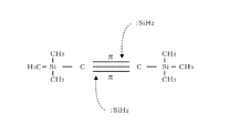
- This is an example of a reaction model related to the chemical reaction formula.
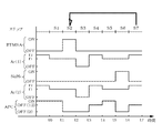
- It is a time chart which shows an example of the film forming method.
- It is a time chart which shows another example of a film forming method.
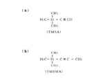
- It is a structural formula showing another example of a carbon precursor.
- This is an example of a reaction model related to the other chemical reaction formula.
- It is explanatory drawing which shows the variation of a carbon precursor.
- It is explanatory drawing which shows the variation of a silicon precursor.
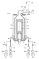
- the film forming apparatus 1 includes a processing container 10 for accommodating a substrate, for example, a semiconductor wafer (hereinafter referred to as “wafer”) W, and the processing container 10 is formed of a metal such as aluminum (Al) in a substantially cylindrical shape.
- a carry-in outlet 11 for carrying in or out the wafer W is formed by a gate valve 12 so as to be openable and closable.
- the exhaust duct 13 is provided with a slit 131 along the inner peripheral surface, and an exhaust port 132 is formed on the outer wall of the exhaust duct 13.
- a top wall 14 is provided on the upper surface of the exhaust duct 13 so as to close the upper opening of the processing container 10 via the insulating member 15, and the exhaust duct 13 and the insulating member 15 are hermetically sealed with a seal ring 16. It will be stopped.
- a mounting table 2 for horizontally supporting the wafer W is provided inside the processing container 10, and the mounting table 2 is made of a ceramic material such as aluminum nitride (AlN) or a metal material such as aluminum or nickel alloy. It is formed in a disk shape.
- a heater 21 forming a heating portion for heating the wafer W is embedded in the mounting table 2, and the outer peripheral region and the side surface of the upper surface of the mounting table 2 are covered members 23 made of ceramics such as alumina. Covered by.
- the mounting table 2 is connected to an elevating mechanism 25 provided below the processing container 10 via a support member 24, and transfers the processing position shown by the solid line in FIG. 1 and the wafer W shown by the alternate long and short dash line below the processing position. It is configured to be able to move up and down with and from the position.
- reference numeral 17 indicates a partition member for vertically partitioning the inside of the processing container 10 when the mounting table 2 is raised to the processing position.
- Three support pins 26 (only two of which are shown) are vertically provided on the lower side of the mounting table 2 in the processing container 10 by an elevating mechanism 27 provided below the processing container 10.
- the support pin 26 is inserted through a through hole 22 of the mounting table 2 at the delivery position so as to be recessable with respect to the upper surface of the mounting table 2, and the external transport mechanism (not shown) and the mounting table 2 are connected to each other. It is used for the transfer of wafers W between.
- Reference numerals 28 and 29 in the drawing refer to bellows that separate the atmosphere inside the processing container 10 from the outside air and expand and contract as the mounting table 2 and the support pin 26 move up and down, respectively.
- the processing container 10 is provided with a shower head 3 for supplying the processing gas in a shower shape in the processing container 10 so as to face the mounting table 2.
- the shower head 3 includes a main body 31 fixed to the top wall 14 of the processing container 10 and a shower plate 32 connected under the main body 31, and the inside thereof forms a gas diffusion space 33. ..
- An annular protrusion 34 projecting downward is formed on the peripheral edge of the shower plate 32, and a gas discharge hole 35 is formed on the flat surface inside the annular protrusion 34.
- the gas supply system 5 is connected to the gas diffusion space 33 via the gas introduction hole 36.
- the gas supply system 5 includes a carbon precursor supply unit configured to supply the carbon precursor gas to the processing container 10 and a silicon precursor supply unit configured to supply the silicon precursor gas. ..
- the carbon precursor supply unit includes a carbon precursor gas supply source 51 and a gas supply path 511, and the gas supply path 511 is provided with a flow rate adjusting unit 512, a storage tank 513, and a valve 514 from the upstream side. NS.
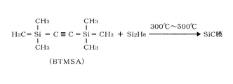
- the carbon precursor contains an organic compound having an unsaturated carbon bond, and for example, bistrimethylsilylacetylene (BTMSA) having a triple bond is used.
- BTMSA bistrimethylsilylacetylene
- the carbon precursor gas supplied from the supply source 51 is temporarily stored in the storage tank 513, boosted to a predetermined pressure in the storage tank 513, and then supplied into the processing container 10.
- BTMSA is a liquid at room temperature, and the gas obtained by heating is supplied to the storage tank 513 and stored.
- the supply and stop of the carbon precursor gas from the storage tank 513 to the processing container 10 is performed by opening and closing the valve 514.
- the silicon precursor supply unit includes a gas supply source 52 and a gas supply path 521 of the silicon precursor, and the gas supply path 521 is provided with a flow rate adjusting unit 522, a storage tank 523, and a valve 524 from the upstream side.
- the silicon precursor contains a silicon compound, and for example, disilane (Si 2 H 6 ) is used.
- the gas of silicon precursor may be referred to as silicon precursor gas or disilane gas.
- the silicon precursor gas supplied from the supply source 52 is temporarily stored in the storage tank 523, boosted to a predetermined pressure in the storage tank 523, and then supplied into the processing container 10.
- the supply and stop of the silicon precursor gas from the storage tank 523 to the processing container 10 is performed by opening and closing the valve 524.
- the gas supply system 5 includes supply sources 53 and 54 of an inert gas such as argon (Ar) gas.
- the Ar gas supplied from one of the supply sources 53 is used as a purge gas for carbon precursor gas.
- the supply source 53 is connected from the upstream side to the downstream side of the valve 514 in the gas supply path 511 of the carbon precursor gas via the gas supply path 531 provided with the flow rate adjusting unit 532 and the valve 533.
- the Ar gas supplied from the other supply source 54 is used as a purge gas for silicon precursor gas.
- the supply source 54 is connected from the upstream side to the downstream side of the valve 524 in the gas supply path 521 of the silicon precursor gas via the gas supply path 541 provided with the flow rate adjusting unit 542 and the valve 543.
- the supply and stop of Ar gas to the processing container 10 is performed by opening and closing valves 533 and 543.
- the processing container 10 is connected to a vacuum exhaust passage 62 via an exhaust port 132, and a vacuum pump configured to execute vacuum exhaust of the gas in the processing container 10 on the downstream side of the vacuum exhaust passage 62, for example.
- a vacuum exhaust unit 61 is provided in the vacuum exhaust passage 62.
- an APC (Auto pressure Controller) valve 63 is interposed between the processing container 10 and the vacuum exhaust portion 61 as a pressure control valve.
- the pressure inside the processing container 10 is adjusted by a pressure adjusting mechanism.
- the pressure adjusting mechanism of this example includes a vacuum exhaust section 61, a vacuum exhaust passage 62, and an APC valve (pressure adjusting valve) 63.
- the APC valve 63 is composed of, for example, a butterfly valve, and is provided with a vacuum exhaust passage 62 that can be opened and closed, and has a role of adjusting the pressure in the processing container 10 by increasing or decreasing the conductance of the vacuum exhaust passage 62 by adjusting the opening degree thereof. Fulfill.
- the APC valve 63 is opened and closed to adjust the pressure in the processing container 10, and by reducing the opening degree, the exhaust in the processing container 10 is hindered and the exhaust flow rate decreases. .. Further, in the vacuum exhaust passage 62, for example, a pressure detection unit 64 is provided between the exhaust port 132 and the APC valve 63. The pressure detection unit 64 is provided in the immediate vicinity of the exhaust port 132, and the pressure detection value can be regarded as the pressure detection value in the processing container 10.
- the APC valve 63 in this example has a pressure adjusting function and an opening degree setting function.
- the pressure adjusting function is a function of controlling the pressure by adjusting the opening degree based on the pressure detected value by the pressure detecting unit 64 and the preset pressure target value.
- the opening degree setting function is a function of fixing the opening degree of the valve body to a preset opening degree. Then, in the film formation process of the SiC film described later, the pressure adjusting function and the opening degree setting function are switched based on the command from the control unit 100.
- the control unit 100 is composed of, for example, a computer, and includes a data processing unit including a program, a memory, and a CPU.
- a control signal is sent from the control unit 100 to each part of the film forming apparatus 1, and a command (each step) is incorporated so as to proceed with the film forming process of the SiC film described later.
- the program is stored in a storage unit such as a computer storage medium such as a flexible disk, a compact disk, a hard disk, or an MO (magneto-optical disk) and installed in the control unit 100.
- control unit 100 is configured to control the film forming process for forming the SiC film on the wafer W.
- a suction step of supplying BTMSA gas as a carbon precursor to adsorb BTMSA on the wafer W is performed.
- a reaction step is carried out in which disilane gas is supplied as a silicon precursor to react BTMSA adsorbed on the wafer W with disilane.
- the adsorption step and the reaction step are alternately repeated a plurality of times to control the formation of a SiC film by the ALD (Atomic layer deposition) method.
- ALD Atomic layer deposition
- control unit 100 is configured to control the vacuum exhaust by the vacuum exhaust unit 61 in the suction step and temporarily limit the vacuum exhaust in the processing container 10. In this vacuum exhaust control, after the carbon precursor gas is retained in the processing container 10, the restriction on the vacuum exhaust is released, and the control is performed so that the carbon precursor gas in the processing container 10 is discharged.
- control unit 100 starts limiting the vacuum exhaust during the period of supplying the carbon precursor gas to the processing container 10, and after a predetermined time has elapsed from the stop of the supply of the gas, the limitation is described. Is configured to control the termination of. Furthermore, during the reaction step, the supply of silicon precursor gas to the processing container 10 is stopped, and after the supply is stopped, the vacuum exhaust unit 61 executes control to continue vacuum exhaust so as not to limit the vacuum exhaust. It is configured to do.
- the film formation method of the present disclosure uses a carbon precursor gas and a silicon precursor gas, and forms a SiC film by a thermal reaction of 500 ° C. or lower without using plasma by the ALD method. It is a thing.
- FIG. 2 shows an example in which BTMSA having a triple bond, which is a carbon precursor, and disilane, which is a silicon precursor, are thermally reacted at a temperature in the range of, for example, 300 ° C. or higher and 500 ° C. or lower.
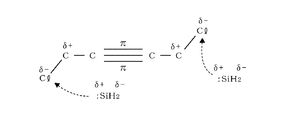
- reaction model 1 The mechanism by which a SiC film can be formed by such a thermal reaction at a low temperature will be considered using the reaction model 1 shown in FIG.
- Disilane is thermally decomposed by heating at around 400 ° C. to generate a SiH 2 radical having an unpaired electron in the Si atom, and this SiH 2 radical has an empty p-orbital.
- this empty p-orbital acts as an electrophile that attacks the ⁇ bond of the unsaturated carbon bond of BTMSA, which is rich in electrons, and acts on the triple bond of BTMSA.
- C forming the triple bond reacts with Si of the SiH 2 radical to form a SiC bond.
- the reaction model 1 is for inferring the reason why the SiC film can be formed at a low temperature, which has been considered difficult in the past, and does not limit the actual reaction route. If the SiC film can be formed at a temperature of 500 ° C. or lower without using plasma, the SiC film may be formed via another reaction path.
- FIGS. 4A and 4B show the timing of starting and stopping the supply of BTMSA gas, Ar gas, and disilane gas, and the timing of opening and closing the APC valve 63, respectively.
- BTMSA gas and disilane gas "ON" on the vertical axis indicates a supply state, and "OFF" indicates a supply stop state, respectively.
- Ar (1) shown in FIGS. 4A and 4B refers to Ar gas for purging BTMSA gas
- Ar (2) in FIG. 4B refers to Ar gas for purging disilane gas, respectively.
- "ON” of the APC valve 63 means that the pressure adjusting function of the APC valve 63 is set to “ON” and the opening degree is adjusted so as to approach the pressure target value based on the pressure detection value.
- "OFF” of the APC valve 63 means that the pressure adjusting function is set to “OFF” and the opening degree of the APC valve 63 is adjusted to the set opening degree by the opening degree setting function.
- “OFF (0)” means that the opening degree is set to 0%, that is, the fully closed state
- “OFF (12)” means that the opening degree is set to 12%.
- the film forming process will be described with reference to FIG. 4A.
- a step of carrying the wafer W into the processing container 10, closing the gate valve 12 of the processing container 10, and accommodating the wafer W in the processing container 10 is performed.
- the heating of the wafer W by the heater 21 is started, and the vacuum exhaust unit 61 performs vacuum exhaust in the processing container 10.
- the APC valve 63 sets the pressure adjusting function to "ON”, performs opening / closing control based on the pressure detection value from the pressure detection unit 64, and controls the inside of the processing container 10 to a pressure target value of, for example, 1000 Pa.
- Ar (1) and (2) which are purge gases, are supplied into the processing container 10 at a first flow rate r1 such as 50 sccm, respectively, and the first pressure adjustment step S1 is executed.
- Ar (1) and (2) are introduced into the processing container 10 via the shower head 3 and flow toward the exhaust port 132 on the side of the wafer W placed on the mounting table 2 at the processing position. , Is discharged from the processing container 10 via the vacuum exhaust passage 62.
- the valve 514 is opened to start supplying the gas of BTMSA, which is a carbon precursor, to the processing container 10, and the adsorption step of adsorbing BTMSA on the wafer W is started.
- BTMSA gas stored in the storage tank 513
- the BTMSA supply step S2 is carried out.
- Ar (1) and Ar (2) continue to be supplied at the first flow rate r1.
- the valve 514 is closed to stop the supply of BTMSA, and the BTMSA filling step S3 is performed.
- the supply of Ar (1) and Ar (2) is stopped.
- the adsorption step comprises a BTMSA supply step S2 and a BTMSA encapsulation step S3.
- the heater 21 heats the wafer W to a temperature in the range of 300 ° C. or higher and 500 ° C. or lower, for example, 410 ° C. ..
- the BTMSA encapsulation step S3 is provided after the BTMSA supply step S2, and the BTMSA gas is retained in the processing container 10 by temporarily limiting the vacuum exhaust in the processing container 10 during these periods.
- the control of the APC valve 63 is switched to the opening degree setting function, and the opening degree is set to "0%", that is, in the fully closed state.
- the exhaust gas in the processing container 10 is temporarily substantially stopped during the period of the BTMSA supply step S2 and the BTMSA filling step S3. Therefore, by performing the above operation, it is possible to maintain a state in which the BTMSA gas is filled and stays in the processing space formed between the shower head 3 and the mounting table 2.
- the APC valve 63 does not have a function of separating the upstream side and the downstream side thereof, and even if the APC valve 63 is set to the fully closed state, gas may continue to be discharged from the processing container 10 although the amount is small. Even in such a case, it has been confirmed that the effect of retaining BTMSA gas in the processing container 10 can be obtained as compared with the case where the APC valve 63 is in the open state.
- the residence time of BTMSA gas in the processing container 10 is extended as compared with the case where vacuum exhaust is continued, and the time for contacting BTMSA gas with the wafer W can be lengthened.
- the time required for the chemical adsorption can be sufficiently secured, so that a sufficient amount of BTMSA is applied to the surface of the wafer W. Can be adsorbed.
- the temporary restriction of the vacuum exhaust in the processing container 10 is implemented by making the opening degree of the APC valve 63 smaller than before the restriction is started. Therefore, not only the case where the APC valve 63 is fully closed as in the above-mentioned example, but also the case where the opening degree of the APC valve 63 is made smaller than before the restriction is started is included. If the opening degree of the APC valve 63 is made smaller than that before the start of the limitation, the exhaust of the carbon precursor gas in the processing container 10 is suppressed and the exhaust flow rate is lowered, so that the gas stays in the processing container 10. .. Therefore, depending on the type of gas of the carbon precursor and the film quality of the target SiC film, the organic compound in the gas may be sufficiently adsorbed on the wafer W even if the APC valve 63 is not fully closed. May be possible.
- the opening degree of the APC valve 63 is set to, for example, 12%, and Ar (1) and (2) are supplied at a second flow rate r2, for example, 500 sccm, respectively, and the first purge step is performed.
- the opening degree of the APC valve 63 is fixed at 12% to promote forced exhaust in the processing container 10.
- step S5 the opening degree of the APC valve 63 is adjusted based on the pressure detection value so that the inside of the processing container 10 approaches the pressure target value.
- the second pressure adjustment step in step S5 may be omitted in order to improve throughput and the like.
- the adsorption step is from time t1 to time t3 when the Ar gas purge is started. Then, the temporary restriction of the vacuum exhaust starts at time t1 during the period of supplying the BTMSA gas to the processing container 10 and ends at t3 after the elapse of the preset time. Therefore, the period after the supply of BTMSA gas is stopped at time t2 is also included in the period in which the vacuum exhaust is restricted.
- the time t3 is appropriately set depending on the type of gas of the carbon precursor, the target film quality of the SiC film, and the like. As an example, the supply time of BTMSA gas is 1 second, and the time for temporarily limiting the vacuum exhaust is 3 seconds or more, preferably 10 seconds or more.
- the pressure inside the processing container 10 fluctuates by temporarily limiting the vacuum exhaust of the processing container 10, but as described above, the BTMSA gas supply time and the vacuum exhaust are temporarily limited. The time to do is short. Therefore, the amount of pressure fluctuation in the processing container 10 is not so large, and there is no great influence that deteriorates the film quality of the formed SiC film.
- the valve 524 is opened to start the supply of disilane gas, which is a silicon precursor, and the disilane supply step S6 is carried out.
- This step S6 is a reaction step of reacting BTMSA adsorbed on the wafer W with disilane.
- the disilane gas is supplied for a relatively short time, for example, 1 second, until the valve 524 is closed and the supply is stopped at time t6.
- the disilane gas stored in the storage tank 523 is supplied into the processing container 10 in a short time.
- Ar (1) and Ar (2) are supplied at the first flow rate r1.
- the disilane gas is retained in the processing container 10 by temporarily limiting the vacuum exhaust in the processing container 10.
- the control of the APC valve 63 is switched to the opening setting function, and the opening is set to "0%", that is, in the fully closed state. That is, the exhaust gas in the processing container 10 is temporarily and substantially stopped for a relatively short time until the supply of the disilane gas is started at the time t5 and the supply is stopped at the time t6. Therefore, by performing the above operation, the processing space formed between the shower head 3 and the mounting table 2 is in contact with the BTMSA adsorbed on the wafer W in a state of being filled with disilane gas and reacts. Form SiC.
- the opening degree of the APC valve 63 is set to, for example, 12%, Ar (1) and (2) are supplied at the second flow rate r2, respectively, and the second purge step S7 is performed. do.
- the forced exhaust in the processing container 10 is advanced by fixing the opening degree of the APC valve 63 to 12%. As a result, the excess disilane gas and Ar gas in the processing container 10 are quickly discharged from the processing container 10. After that, steps 2 to 7 are repeated again.
- the vacuum exhaust of the processing container 10 may be controlled to be continued without temporarily limiting the vacuum exhaust. Since the time chart of FIG. 4B is the same as that of FIG. 4A except for the control of the APC valve 63 in the disilane supply step S6, the description other than the APC valve 63 of the step S6 will be omitted.
- the APC valve 63 switches the pressure adjustment function to “ON” at the time t4 when the second pressure adjustment step S5 is started, and the processing container is also based on the pressure detection value in the disilane gas supply step S6. The opening degree is adjusted so that the inside of 10 approaches the pressure target value.
- the disilane gas introduced from the shower head 3 flows through the processing container 10 toward the exhaust port 132 and reacts with the BTMSA adsorbed on the wafer W to form SiC.
- amorphous Si When the excess disilane gas is decomposed on the surface of the wafer W, amorphous Si may be deposited and an amorphous Si film may be formed. Therefore, as shown in FIG. 4A, the purging is performed immediately after the supply of the disilane gas is stopped, or as shown in FIG. 4B, the vacuum exhaust in the processing container 10 is continued during the supply period of the disilane gas. In other words, in the disilane gas, the formation of the amorphous Si film can be suppressed by not providing the encapsulation step like BTMSA and not limiting the vacuum exhaust after the supply of the disilane gas is stopped.
- the gas supply of BTMSA which is the carbon precursor of step S2
- the step of adsorbing BTMSA on the wafer W and the step of reacting BTMSA with disilane are alternately performed by the method described above.
- the SiC film thus formed by the ALD method is surely formed with a SiC bond.
- XPS X-ray Photoelectron Spectroscopy
- the vacuum exhaust in the processing container 10 is restricted and the BTMSA gas stays in the processing container 10. I'm letting you. Therefore, as described above, the chemical adsorption of BTMSA on the wafer surface is promoted, a SiC film having good film quality can be formed, and the film formation rate can be improved.
- a SiC film having a good film quality is a film having a good ratio (Si / C ratio) of a silicon (Si) component and a carbon (C) component in the SiC film, and specifically, the Si / C ratio is 1. It is a film close to. From the examples described later, it is recognized that the carbon atom (C) having a SiC bond in the SiC film is increased by the method of the present disclosure.
- the vacuum exhaust in the processing container 10 is not restricted at least after the supply of disilane gas is stopped (steps 4A and 4B). S7). Therefore, excess disilane gas not used for the reaction with BTMSA is rapidly discharged from the processing container 10, and the formation of the above-mentioned amorphous Si film is suppressed. Therefore, from this point as well, the increase of the Si component in the SiC film can be suppressed, the formation of the amorphous Si film can be suppressed, and a film having a good Si / C ratio can be formed.
- a silicon precursor for example, disilane gas
- the SiC film formed by thermally reacting the carbon precursor and the silicon precursor at a relatively low temperature of 300 ° C. or higher and 500 ° C. or lower using the ALD method is of high quality, and is a hard mask material, an insulating film, or the like. It has properties suitable for a low dielectric constant film.
- the allowable temperature during the film forming process is 500 ° C. or less in order to suppress the diffusion of metal from the metal wiring layer. On the other hand, even if it is possible to form a film at a low temperature of 400 ° C.
- the method of forming a SiC film using plasma causes great damage to other films and wiring layers constituting the semiconductor element due to plasma. Therefore, it may be a problem. Therefore, it is effective that the SiC film can be formed at a temperature of 500 ° C. or lower without using plasma by the film forming method of the present disclosure, which leads to the expansion of applications of the SiC film.
- BTMSA has less intramolecular polarization (localization of electric charge) and is less likely to be chemically adsorbed to the surface of the wafer W than a molecule having a large amount of polarization. Therefore, in a method such as the ALD method in which the supply of BTMSA gas is repeated for a short time, if vacuum exhaust is performed in the adsorption step, BTMSA may be discharged from the processing container 10 before being sufficiently chemically adsorbed. .. As a result, there are problems that the C component in the SiC film is reduced, the desired SiC film having a Si / C ratio cannot be formed, and the film formation rate is low.
- the limitation of the vacuum exhaust in the processing container 10 is implemented by reducing the opening degree of the APC valve 63, so that it is easy to control. Furthermore, when BTMSA is used as the carbon precursor, BTMSA does not form a thermal decomposition film by itself, so that there is an advantage that a SiC film can be easily formed by the ALD method.
- the carbon precursor shown in FIG. 5 (a) is trimethylsilylacetylene (TMSA) having a triple bond.
- the carbon precursor shown in FIG. 5B is trimethylsilylmethylacetylene (TMSMA) having a triple bond.
- TMSA trimethylsilylacetylene
- TMSMA trimethylsilylmethylacetylene
- a SiC film can also be formed by thermally reacting these TMSA gas and TMSMA gas with a silicon precursor, for example, disilane gas, at a temperature in the range of 300 ° C. or higher and 500 ° C. or lower.
- TMSA and TMSMA also have less intramolecular polarization and are less likely to cause chemisorption on the wafer surface, but chemical adsorption with the wafer can be promoted by temporarily limiting vacuum exhaust in the adsorption step.
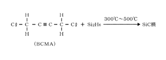
- the carbon precursor shown in FIG. 6 is bischloromethylacetylene (BCMA) having a triple bond which is an unsaturated carbon bond and containing a halogen.
- FIG. 6 shows an example in which a BCMA gas and a silicon precursor, for example, disilane gas, are thermally reacted at a temperature in the range of 300 ° C. or higher and 500 ° C. or lower. Regarding this thermal reaction, it is presumed that the reaction model 1 shown in FIG. 3 and the reaction model 2 shown in FIG. 7 proceed at the same time.
- the reaction model 2 has nucleophilicity in which BCMA is polarized by having a halogen group (Cl group) and the positive polarization site ( ⁇ +) of the SiH 2 radical attacks the negative polarization site ( ⁇ ). In this way, the SiH 2 radical reacts with C at the molecular end where Cl is bonded to form a SiC bond.
- the carbon precursor containing an organic compound having an unsaturated carbon bond is not limited to the above-mentioned BTMSA, TMSA, TMSMA and BCMA. If the thermal reaction with the silicon precursor proceeds at a temperature of 500 ° C. or lower and it is possible to form a SiC film, another carbon precursor may be used.
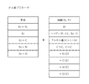
- the carbon precursor a combination of a skeleton and a side chain shown in FIG. 8 can be used.
- the skeleton of the carbon precursor is an unsaturated bond portion of an organic compound, and can exemplify the unsaturated carbon bond of a triple bond or a double bond of C.
- the side chain of the carbon precursor is the part that is attached to the skeleton.
- the side chain that binds to one C is X
- the side chain that binds to the other C is Y.
- These side chains X and Y may be the same as each other or may be different from each other.
- Side chains include hydrogen (H) atoms, halogens, alkyl groups with a C number of 5 or less, triple bonds of C, double bonds of C, Si (Z), C (Z), N (Z), O. (Z) and the like can be mentioned.
- Si (Z), C (Z), N (Z), and O (Z) are the sites where the skeleton is bonded to C, which is Si, C, N. , O, and (Z) indicates an arbitrary atomic group.
- the silicon precursor a combination of a skeleton and a side chain shown in FIG. 9 can be used.
- the skeleton of the silicon precursor is a Si—Si bond in terms of disilane.
- the side chain of the silicon precursor is the part that is attached to the skeleton. Assuming that the skeleton is Si—Si, the side chain X that binds to one Si and the side chain Y that binds to the other Si may be the same or different from each other. Examples of the skeleton include Si—Si, Si, Si—C, Si—N, Si—O and the like.
- Side chains include hydrogen atoms, halogens, alkyl groups with a C number of 5 or less, triple bonds of C, double bonds of C, Si (Z), C (Z), N (Z), O (Z). And so on.
- silicon precursors that thermally decompose at a temperature of 500 ° C. or lower to generate SiH 2 radicals include disilane, monosilane (SiH 4 ), trisilane (Si 3 H 8 ), and the like.
- FIG. 10 is a time chart showing the timing of starting and stopping the supply of the gas of BTMSA which is a carbon precursor and the disilane gas which is a silicon precursor, and the opening / closing control of the APC valve 63.
- the purge gases Ar (1) and (2) are not shown respectively, but these purge gases are supplied in the same manner as in the time charts shown in FIGS. 4A and 4B, so the description is given. Omitted. Other than that, how to read the time chart is the same as in FIGS. 4A and 4B.
- the temporary restriction of the vacuum exhaust is controlled so as to start after stopping the supply of the carbon precursor gas to the processing container 10 and then ending after the elapse of a preset time. ..
- the BTMSA gas opens the valve 514 at time t1 to start the supply, closes the valve 514 at the time t2, and stops the supply.
- the disilane gas opens the valve 524 at time t4 to start the supply, and closes the valve 524 at the time t5 to stop the supply.
- the APC valve 63 sets the pressure adjusting function to "ON" until time t2, that is, while the BTMSA gas is being supplied, and controls the pressure in the processing container 10.
- the supply of BTMSA gas is stopped, the APC valve 63 is fully closed, and the temporary restriction of vacuum exhaust is started.
- the exhaust flow rate decreases in the processing container 10
- the BTMSA gas stays, and the chemisorption of BTMSA on the wafer W proceeds.
- the opening degree of the APC valve 63 was set to, for example, "12%" and vacuum exhaust was performed. The temporary restriction of the above is terminated, and the inside of the processing container 10 is forcibly exhausted.
- the pressure adjustment function of the APC valve 63 is set to "ON" when the disilane gas is supplied, but as in FIG. 4A, the APC valve 63 is switched to the opening setting function and fully closed only when the disilane gas is supplied. It may be in a state. In this case, the supply of the disilane gas is stopped, the opening degree of the APC valve 63 is set to, for example, "12%", purging is performed, the inside of the processing container 10 is forcibly exhausted, and the excess disilane gas is discharged.
- the vacuum exhaust of the processing container 10 may be temporarily restricted in the adsorption step of adsorbing the organic compound of the carbon precursor on the wafer W. Therefore, it is not essential to start limiting the vacuum exhaust in conjunction with the supply and stop operations of the carbon precursor.
- the restriction of vacuum exhaust may be started slightly later than the time t1 of FIGS. 4A and 4B, which is the timing of starting the supply of the carbon precursor gas to the processing container 10.
- the restriction of vacuum exhaust may be started slightly later than the time t2 in FIG. 10, which is the timing when the supply of the carbon precursor gas to the processing container 10 is stopped.
- a wafer boat 72 for loading a large number of wafers W in a shelf shape is airtightly housed inside a reaction tube 71, which is a processing container made of quartz glass, from the lower side.
- a reaction tube 71 which is a processing container made of quartz glass, from the lower side.
- two gas injectors 73 and 74 are arranged so as to face each other via the wafer boat 72 in the length direction of the reaction tube 71.
- the gas injector 73 is connected to a gas supply source 811 of a carbon precursor, for example, BTMSA, via, for example, a gas supply path 81. Further, the gas injector 73 is connected to a supply source 821 of purge gas, for example Ar gas, via, for example, a branch path 82 branching from the gas supply path 81.
- the gas supply path 81 is provided with a flow rate adjusting unit 812, a storage tank 813, and a valve 814 from the upstream side, and the branch path 82 is provided with a flow rate adjusting unit 822 and a valve 823 from the upstream side.
- the carbon precursor supply unit that supplies the carbon precursor gas to the reaction tube 71 includes the gas supply path 81 and the BTMSA gas supply source 811.
- the gas injector 74 is connected to a silicon precursor, for example, a disilane gas supply source 831 via, for example, a gas supply path 83. Further, the gas injector 74 is connected to the supply source 841 of Ar gas, which is a purge gas, via, for example, a branch path 84 branching from the gas supply path 83.
- Ar gas which is a purge gas
- a flow rate adjusting unit 832, a storage tank 833, and a valve 834 are interposed in the gas supply path 83 from the upstream side, and a flow rate adjusting section 842 and a valve 843 are interposed in the branch path 84 from the upstream side.
- the silicon precursor supply unit that supplies the silicon precursor gas to the reaction tube 71 includes the gas supply path 83 and the disilane gas supply source 831.
- An exhaust port 75 is formed at the upper end of the reaction tube 71, and the exhaust port 75 is connected to a vacuum exhaust section 852 composed of a vacuum pump via a vacuum exhaust path 85 provided with an APC valve 851 forming a pressure control valve. Will be done. Further, the vacuum exhaust passage 85 is provided with a pressure detection unit 853 on the upstream side of the APC valve 851.
- the function of the APC valve 851 is the same as the configuration example shown in FIG. 1 above.
- reference numeral 76 refers to a lid for opening and closing the lower end opening of the reaction tube 71
- 77 refers to a rotation mechanism for rotating the wafer boat 72 around a vertical axis.
- a heating unit 78 is provided around the reaction tube 71 and around the lid portion 76 to heat the wafer W placed on the wafer boat 72 to a temperature within a range of, for example, 300 ° C. or higher and 500 ° C. or lower.
- a film forming process for forming a SiC film is performed according to the time chart shown in FIGS. 4A, 4B or 10.
- a step of carrying a wafer boat 72 carrying a plurality of wafers W into the reaction tube 71, closing the lid portion 76 of the reaction tube 71, and accommodating the wafer W in the reaction tube 71 is performed.
- the inside of the reaction tube 71 is evacuated, the valves 823 and 843 are opened to supply Ar gas, and the inside of the reaction tube 71 has a pressure target value of 400 Pa, a set temperature of 300 ° C. or higher and a temperature of 500 ° C. or lower, for example, 390. Control to °C respectively.
- the valve 814 is opened, the gas of BTMSA, which is a carbon precursor, is supplied into the reaction tube 71, and the step of adsorbing BTMSA on the wafer W is carried out. Subsequently, after closing the valve 814 and stopping the supply of BTMSA gas, the inside of the reaction tube 71 is purged with Ar gas. Next, a step of opening the valve 834 to supply disilane gas, which is a silicon precursor, and reacting BTMSA adsorbed on the wafer W with disilane to form a SiC film is carried out. After that, the valve 834 is closed to stop the supply of disilane gas, and then the inside of the reaction tube 71 is purged with Ar gas. The adsorption step of BTMSA and the reaction step of BTMSA and disilane are alternately repeated a plurality of times to form a SiC film having a predetermined film thickness.
- the APC valve 851 is fully closed to temporarily limit the vacuum exhaust in the reaction tube 71, and the BTMSA gas is retained in the reaction tube 71. After that, the APC valve 851 is opened to release the temporary restriction on vacuum exhaust, and BTMSA gas is discharged from the reaction tube 71. Further, during the reaction step, the supply of disilane gas to the reaction tube 71 is stopped, and after the supply is stopped, the vacuum exhaust is not restricted, and the pressure adjustment function of the APC valve 63 is set to "ON" for the reaction. The pressure inside the pipe 71 is controlled. Specifically, for example, various gases are supplied and the opening degree of the APC valve 851 is adjusted according to the time chart of FIG. 4A, FIG.
- the vacuum exhaust of the reaction tube 71 is temporarily restricted, while in the step of reacting BTMSA adsorbed on the wafer W with disilane, disilane gas is supplied. After the stop, the vacuum exhaust is not temporarily restricted. Therefore, as in the embodiment described with reference to FIGS. 1, 4A, 4B, 10 and the like, a SiC film having good film quality can be formed at a high film forming rate.
- the temporary limitation of the vacuum exhaust is not limited to the case where the vacuum exhaust is implemented by controlling the opening degree of the APC valve 63.
- the exhaust amount of the vacuum exhaust unit may be reduced, or the vacuum exhaust unit may be stopped.
- FIG. 12 is a characteristic diagram showing the amount of film formed when a SiC film is formed by the ALD method using BTMSA as a carbon precursor, disilane as a silicon precursor, and Ar gas as a purge gas in the film forming apparatus 1 shown in FIG. Is.
- the wafer W is heated while supplying Ar gas into the processing container 10, the pressure in the processing container 10 is adjusted to the pressure target value, and then steps 1 to 8 shown below are performed in step 1. From step 8 to step 8 in order.
- Step 1 With the pressure adjustment function of the APC valve 63 set to "ON”, the inside of the processing container 10 is evacuated for 3 seconds, and then the pressure adjustment function of the APC valve 63 is switched to "OFF" (fully closed state).
- Step 2 While the APC valve 63 is in the "OFF” state (fully closed state), BTMSA gas is supplied for 1 second to adsorb BTMSA to the wafer.
- Step 3 The APC valve 63 is in the "OFF” state (fully closed state). ), The supply of BTMSA gas is stopped, and the BTMSA gas is retained in the processing container 10 for x seconds.
- Step 4 The pressure adjustment function of the APC valve 63 is switched to "ON" to control the pressure in the processing container 10.
- Step 5 The process of supplying Ar gas for 5 seconds and purging the inside of the processing container 10 while performing the above steps.
- Step 6 Set the pressure adjustment function of the APC valve 63 to "OFF" and set it to the fully closed state.
- Step 6 While keeping the APC valve 63 in the "OFF" state (fully closed state), disilane gas is applied.
- Step 7 A step of supplying disilane gas for y seconds while keeping the APC valve 63 in the "OFF" state (fully closed state)
- Step 8 APC valve 63 The step of supplying Ar gas for 5 seconds and purging the inside of the processing container 10 while controlling the pressure inside the processing container 10 by switching the pressure adjustment function of
- the film forming process is performed under the process conditions described above, and in steps 3 and 7, the time for setting the APC valve 63 to the fully closed state (valve closing time) is set to the residence time of BTMSA gas x seconds and the residence time of disilane gas, respectively. It was set to y seconds.
- valve closing time is set to the residence time of BTMSA gas x seconds and the residence time of disilane gas, respectively. It was set to y seconds.
- a SiC film formed under the condition that a residence time is provided only in the BTMSA gas x seconds in step 3 is 3 seconds, 10 seconds, y seconds in step 7 is 0 seconds.
- Comparative Example 1 a SiC film formed under the condition that both BTMSA gas and disilane gas have a residence time (x seconds in step 3 is 3 seconds, y seconds in step 7 is 3 seconds).
- Comparative Example 2 is a conventional method, that is, a SiC film formed under the condition that no residence time is provided in both BTMSA gas and disilane gas (x seconds in step 3 is 0 seconds, y seconds in step 7 is 0 seconds).
- Comparative Example 3 is a SiC film formed under the condition that the residence time is provided only in the disilane gas (x seconds in step 3 is 0 seconds, y seconds in step 7 is 3 seconds, 10 seconds).
- the horizontal axis represents the valve closing time
- the vertical axis represents the film thickness (film thickness ( ⁇ ) per cycle).
- the film thickness for calculating the film formation amount was measured by SEM (Scanning Electron Microscope). These film formation amounts are indicated by ⁇ in Example 1, ⁇ in Comparative Example 1, and ⁇ in Comparative Example 3. Further, since the data of Comparative Example 2 corresponds to the data of the valve closing time of Comparative Example 3 at 0 seconds, the illustration is omitted.
- Example 1 it was confirmed that the amount of film formed increased by setting the valve closing time longer. It is understood that this makes it possible to improve the film formation rate by temporarily limiting the vacuum exhaust in the processing container 10 and retaining the BTMSA gas.
- Comparative Example 1 and Comparative Example 3 each have a larger amount of film formation, but as is clear from the following evaluation test 2, an amorphous Si film is used in addition to the SiC film. This is because the film is formed and the apparent amount of film formed is large.
- Si and C based on the SiC bond are increased in the SiC film of Example 1 as compared with the SiC film of Comparative Example 2 formed by the conventional method. It was confirmed that the Si / C ratio was almost 1. As a result, the vacuum exhaust in the processing container 10 is temporarily restricted and the BTMSA gas is retained, so that the Si—C bond in the membrane is increased and the ideal Si / C ratio can be obtained. It was confirmed that the SiC film of the above can be formed. Even when a carbon precursor such as BTMSA, which has less intramolecular polarization and is less likely to be chemically adsorbed on the wafer surface, can be used, a SiC film having good film quality can be formed. In addition, the film formation speed can be improved.
- BTMSA which has less intramolecular polarization and is less likely to be chemically adsorbed on the wafer surface
- Example 1 1.67g / cm 3
- Comparative Example 1 2.01g / cm 3
- Comparative Example 2 2.08g / cm 3
- Comparative Example 3 2.13 g / It was cm 3.
- the film density of Example 1 is smaller than that of Comparative Examples 1 to 3, but in Comparative Examples 1 to 3, the larger the proportion of Si2 (silicon atom having a Si—Si bond), the higher the film density. It is presumed that the difference in film density is due to the formation of an amorphous Si film.
Landscapes
- Chemical & Material Sciences (AREA)
- Engineering & Computer Science (AREA)
- Chemical Kinetics & Catalysis (AREA)
- Organic Chemistry (AREA)
- Metallurgy (AREA)
- Mechanical Engineering (AREA)
- Materials Engineering (AREA)
- General Chemical & Material Sciences (AREA)
- Condensed Matter Physics & Semiconductors (AREA)
- Power Engineering (AREA)
- Microelectronics & Electronic Packaging (AREA)
- Computer Hardware Design (AREA)
- Manufacturing & Machinery (AREA)
- General Physics & Mathematics (AREA)
- Physics & Mathematics (AREA)
- Inorganic Chemistry (AREA)
- Chemical Vapour Deposition (AREA)
Abstract
The present invention comprises: an adsorption step wherein a gas of a carbon precursor that contains an organic compound having an unsaturated carbon bond is supplied into a processing chamber in which a substrate is contained, and the organic compound is caused to adsorb onto the substrate; and a reaction step wherein a gas of a silicon precursor that contains a silicon compound is supplied into the processing chamber, into which the gas of a carbon precursor has been supplied, and the silicon compound and the organic compound adsorbed onto the substrate are caused to react with each other. A silicon carbide-containing film is formed by alternately repeating the adsorption step and the reaction step a plurality of times. In the adsorption step, vacuum evacuation of the processing chamber is restricted, and after having the gas of a carbon precursor remain in the processing chamber, the restriction on vacuum evacuation is lifted. In the reaction step, a silicon carbide-containing film is formed without restricting vacuum evacuation after stopping the supply of the gas of a silicon precursor.
Description
本開示は、炭化ケイ素含有膜を形成する方法及び装置に関する。
The present disclosure relates to a method and an apparatus for forming a silicon carbide-containing film.
半導体素子であるマルチゲート型のFin-FET(Fin-Field Effect Transistor)などにおいては、集積度がさらに高まっており、ハードマスクに形成した開口内に、複数の膜種が露出する場合がある。このため、微細な開口内に露出する膜間で所望の膜を高選択比でエッチングすることが可能なハードマスク材料の必要性が高くなっている。この要請を満たす材料として、発明者らは炭化ケイ素含有膜(以下「SiC膜」という)の成膜技術を開発している。
In multi-gate type Fin-FETs (Fin-Field Effect Transistors), which are semiconductor elements, the degree of integration is further increased, and a plurality of film types may be exposed in the openings formed in the hard mask. Therefore, there is an increasing need for a hard mask material capable of etching a desired film with a high selectivity between films exposed in a fine opening. As a material satisfying this demand, the inventors have developed a film forming technique for a silicon carbide-containing film (hereinafter referred to as "SiC film").
SiC膜については、特許文献1に、アセチレンガスとジクロロシランガスとを反応管内に交互に供給して、900℃~1100℃の高温下でSiC膜を得る手法が記載されている。また、特許文献2には、処理室内にトリエチルアミンガスとジシランガスを同時に供給してSiC膜を形成する手法が記載されている。この手法では、両ガスの同時供給後に圧力調整バルブを閉じて、処理室内にトリエチルアミンガスとジシランガスとを封じ込めることにより、気相反応効率を高めている。
Regarding the SiC film, Patent Document 1 describes a method of alternately supplying acetylene gas and dichlorosilane gas into a reaction tube to obtain a SiC film at a high temperature of 900 ° C. to 1100 ° C. Further, Patent Document 2 describes a method of forming a SiC film by simultaneously supplying triethylamine gas and disilane gas into a treatment chamber. In this method, the pressure adjustment valve is closed after the simultaneous supply of both gases, and the triethylamine gas and the disilane gas are confined in the treatment chamber to improve the gas phase reaction efficiency.
本開示は、膜質が良好な炭化ケイ素含有膜を形成すると共に、成膜速度の向上を図ることができる技術を提供する。
The present disclosure provides a technique capable of forming a silicon carbide-containing film having good film quality and improving the film formation rate.
本開示は、真空排気が行われている処理容器内にて、基板に対して炭化ケイ素含有膜を形成する方法であって、
前記処理容器に前記基板を収容する工程と、
前記基板が収容された前記処理容器に、不飽和炭素結合を有する有機化合物を含む炭素プリカーサのガスを供給し、前記基板に前記有機化合物を吸着させる工程と、
前記炭素プリカーサのガスが供給された後の前記処理容器に、ケイ素化合物を含むケイ素プリカーサのガスを供給し、前記基板に吸着した前記有機化合物と前記ケイ素化合物とを反応させる工程と、を含み、
前記基板に前記有機化合物を吸着させる工程と、前記有機化合物と前記ケイ素化合物とを反応させる工程とを交互に複数回繰り返し、前記炭化ケイ素含有膜を形成することと、
前記有機化合物を吸着させる工程にて、前記真空排気を制限し、前記処理容器内に前記炭素プリカーサのガスを滞留させた後、前記真空排気の制限を解除し、前記処理容器内に滞留する前記炭素プリカーサのガスを排出することと、
前記基板に吸着した前記有機化合物と前記ケイ素化合物とを反応させる工程中に、前記処理容器への前記ケイ素プリカーサのガスの供給を停止し、当該供給停止後は、前記真空排気の制限は行わないことと、を有する。 The present disclosure is a method of forming a silicon carbide-containing film on a substrate in a processing container in which vacuum exhaust is performed.
The step of accommodating the substrate in the processing container and
A step of supplying a carbon precursor gas containing an organic compound having an unsaturated carbon bond to the processing container in which the substrate is housed, and adsorbing the organic compound on the substrate.
A step of supplying the gas of the silicon precursor containing the silicon compound to the processing container after the gas of the carbon precursor is supplied and reacting the organic compound adsorbed on the substrate with the silicon compound is included.
The step of adsorbing the organic compound on the substrate and the step of reacting the organic compound with the silicon compound are alternately repeated a plurality of times to form the silicon carbide-containing film.
In the step of adsorbing the organic compound, the vacuum exhaust is restricted, the gas of the carbon precursor is retained in the processing container, the restriction of the vacuum exhaust is released, and the gas stays in the processing container. Ejecting carbon precursor gas and
During the step of reacting the organic compound adsorbed on the substrate with the silicon compound, the supply of the silicon precursor gas to the processing container is stopped, and after the supply is stopped, the vacuum exhaust is not restricted. It has that.
本開示によれば、膜質が良好な炭化ケイ素含有膜を形成すると共に、成膜速度の向上を図ることができる。
According to the present disclosure, it is possible to form a silicon carbide-containing film having a good film quality and improve the film formation rate.
本開示の炭化ケイ素含有膜を形成する方法(以下、「成膜方法」という)を実施する装置(以下、「成膜装置」という)の一実施形態である枚葉式の成膜装置について、図1を参照し説明する。成膜装置1は、基板例えば半導体ウエハ(以下「ウエハ」という)Wを収容する処理容器10を備え、この処理容器10は、アルミニウム(Al)等の金属により、略円筒形状に構成される。処理容器10の側壁にはウエハWを搬入又は搬出するための搬入出口11が、ゲートバルブ12により開閉自在に形成される。
Regarding a single-wafer film forming apparatus which is an embodiment of an apparatus (hereinafter referred to as "deposition apparatus") for carrying out the method for forming a silicon carbide-containing film of the present disclosure (hereinafter referred to as "deposition method"). This will be described with reference to FIG. The film forming apparatus 1 includes a processing container 10 for accommodating a substrate, for example, a semiconductor wafer (hereinafter referred to as “wafer”) W, and the processing container 10 is formed of a metal such as aluminum (Al) in a substantially cylindrical shape. On the side wall of the processing container 10, a carry-in outlet 11 for carrying in or out the wafer W is formed by a gate valve 12 so as to be openable and closable.
処理容器10の側壁の上部には、例えば断面が矩形形状をなす円環状の排気ダクト13が配置される。この排気ダクト13には、内周面に沿ってスリット131が設けられ、排気ダクト13の外壁には、排気口132が形成される。排気ダクト13の上面には、絶縁部材15を介して処理容器10の上部開口を塞ぐように天壁14が設けられ、排気ダクト13と絶縁部材15との間はシールリング16にて気密に封止される。
An annular exhaust duct 13 having a rectangular cross section, for example, is arranged above the side wall of the processing container 10. The exhaust duct 13 is provided with a slit 131 along the inner peripheral surface, and an exhaust port 132 is formed on the outer wall of the exhaust duct 13. A top wall 14 is provided on the upper surface of the exhaust duct 13 so as to close the upper opening of the processing container 10 via the insulating member 15, and the exhaust duct 13 and the insulating member 15 are hermetically sealed with a seal ring 16. It will be stopped.
処理容器10の内部には、ウエハWを水平に支持するための載置台2が設けられ、この載置台2は、窒化アルミニウム(AlN)等のセラミックス材料や、アルミニウムやニッケル合金等の金属材料で円板状に形成される。この例では、載置台2には、ウエハWを加熱するための加熱部をなすヒータ21が埋設され、載置台2の上面の外周領域及び側面は、アルミナ等のセラミックスにより形成されたカバー部材23により覆われている。
A mounting table 2 for horizontally supporting the wafer W is provided inside the processing container 10, and the mounting table 2 is made of a ceramic material such as aluminum nitride (AlN) or a metal material such as aluminum or nickel alloy. It is formed in a disk shape. In this example, a heater 21 forming a heating portion for heating the wafer W is embedded in the mounting table 2, and the outer peripheral region and the side surface of the upper surface of the mounting table 2 are covered members 23 made of ceramics such as alumina. Covered by.
載置台2は、支持部材24を介して、処理容器10の下方に設けられた昇降機構25に接続され、図1中に実線で示す処理位置と、その下方の一点鎖線で示すウエハWの受け渡し位置との間で昇降自在に構成される。図1中、符号17は、載置台2が処理位置へと上昇した際、処理容器10の内部を上下に区画するための区画部材を指す。処理容器10内の載置台2の下方側には、3本(2本のみ図示)の支持ピン26が、処理容器10の下方に設けられた昇降機構27により昇降自在に設けられる。支持ピン26は、受け渡し位置にある載置台2の貫通孔22に挿通されて載置台2の上面に対して突没可能に構成され、外部の搬送機構(図示せず)と載置台2との間でのウエハWの受け渡しに用いられる。図中符号28、29は、処理容器10内の雰囲気を外気と区画し、夫々載置台2、支持ピン26の昇降動作に伴って伸縮するベローズを指す。
The mounting table 2 is connected to an elevating mechanism 25 provided below the processing container 10 via a support member 24, and transfers the processing position shown by the solid line in FIG. 1 and the wafer W shown by the alternate long and short dash line below the processing position. It is configured to be able to move up and down with and from the position. In FIG. 1, reference numeral 17 indicates a partition member for vertically partitioning the inside of the processing container 10 when the mounting table 2 is raised to the processing position. Three support pins 26 (only two of which are shown) are vertically provided on the lower side of the mounting table 2 in the processing container 10 by an elevating mechanism 27 provided below the processing container 10. The support pin 26 is inserted through a through hole 22 of the mounting table 2 at the delivery position so as to be recessable with respect to the upper surface of the mounting table 2, and the external transport mechanism (not shown) and the mounting table 2 are connected to each other. It is used for the transfer of wafers W between. Reference numerals 28 and 29 in the drawing refer to bellows that separate the atmosphere inside the processing container 10 from the outside air and expand and contract as the mounting table 2 and the support pin 26 move up and down, respectively.
処理容器10には載置台2と対向するように、処理容器10内に処理ガスをシャワー状に供給するためのシャワーヘッド3が設けられる。シャワーヘッド3は、処理容器10の天壁14に固定された本体部31と、本体部31の下に接続されたシャワープレート32と、を備え、その内部はガス拡散空間33を成している。シャワープレート32の周縁部には下方に突出する環状突起部34が形成され、環状突起部34の内側の平坦面には、ガス吐出孔35が形成される。ガス拡散空間33にはガス導入孔36を介して、ガス供給系5が接続される。
The processing container 10 is provided with a shower head 3 for supplying the processing gas in a shower shape in the processing container 10 so as to face the mounting table 2. The shower head 3 includes a main body 31 fixed to the top wall 14 of the processing container 10 and a shower plate 32 connected under the main body 31, and the inside thereof forms a gas diffusion space 33. .. An annular protrusion 34 projecting downward is formed on the peripheral edge of the shower plate 32, and a gas discharge hole 35 is formed on the flat surface inside the annular protrusion 34. The gas supply system 5 is connected to the gas diffusion space 33 via the gas introduction hole 36.
ガス供給系5は、処理容器10に炭素プリカーサのガスを供給するように構成される炭素プリカーサ供給部と、ケイ素プリカーサのガスを供給するように構成されるケイ素プリカーサ供給部と、を備えている。炭素プリカーサ供給部は、炭素プリカーサのガスの供給源51及びガス供給路511を含むものであり、ガス供給路511には、上流側から流量調整部512、貯留タンク513及びバルブ514が介設される。
The gas supply system 5 includes a carbon precursor supply unit configured to supply the carbon precursor gas to the processing container 10 and a silicon precursor supply unit configured to supply the silicon precursor gas. .. The carbon precursor supply unit includes a carbon precursor gas supply source 51 and a gas supply path 511, and the gas supply path 511 is provided with a flow rate adjusting unit 512, a storage tank 513, and a valve 514 from the upstream side. NS.
炭素プリカーサは不飽和炭素結合を有する有機化合物を含むものであり、例えば三重結合を有するビストリメチルシリルアセチレン(BTMSA)が用いられる。以下、炭素プリカーサのガスを炭素プリカーサガス、BTMSAガスと称する場合もある。供給源51から供給される炭素プリカーサガスは、貯留タンク513に一旦貯留されて、当該貯留タンク513内で所定の圧力に昇圧された後、処理容器10内に供給される。BTMSAは常温で液体であり、加熱により得られたガスが貯留タンク513に供給され、貯留される。貯留タンク513から処理容器10への炭素プリカーサガスの供給及び停止は、バルブ514の開閉により行われる。
The carbon precursor contains an organic compound having an unsaturated carbon bond, and for example, bistrimethylsilylacetylene (BTMSA) having a triple bond is used. Hereinafter, the carbon precursor gas may be referred to as carbon precursor gas or BTMSA gas. The carbon precursor gas supplied from the supply source 51 is temporarily stored in the storage tank 513, boosted to a predetermined pressure in the storage tank 513, and then supplied into the processing container 10. BTMSA is a liquid at room temperature, and the gas obtained by heating is supplied to the storage tank 513 and stored. The supply and stop of the carbon precursor gas from the storage tank 513 to the processing container 10 is performed by opening and closing the valve 514.
ケイ素プリカーサ供給部は、ケイ素プリカーサのガスの供給源52及びガス供給路521を含むものであり、ガス供給路521には、上流側から流量調整部522、貯留タンク523及びバルブ524が介設される。ケイ素プリカーサはケイ素化合物を含むものであり、例えばジシラン(Si2H6)が用いられる。ここでは、ケイ素プリカーサのガスをケイ素プリカーサガス、ジシランガスと称する場合もある。供給源52から供給されるケイ素プリカーサガスは、貯留タンク523にて一旦貯留されて、当該貯留タンク523内で所定の圧力に昇圧された後、処理容器10内に供給される。貯留タンク523から処理容器10へのケイ素プリカーサガスの供給及び停止は、バルブ524の開閉により行われる。
The silicon precursor supply unit includes a gas supply source 52 and a gas supply path 521 of the silicon precursor, and the gas supply path 521 is provided with a flow rate adjusting unit 522, a storage tank 523, and a valve 524 from the upstream side. NS. The silicon precursor contains a silicon compound, and for example, disilane (Si 2 H 6 ) is used. Here, the gas of silicon precursor may be referred to as silicon precursor gas or disilane gas. The silicon precursor gas supplied from the supply source 52 is temporarily stored in the storage tank 523, boosted to a predetermined pressure in the storage tank 523, and then supplied into the processing container 10. The supply and stop of the silicon precursor gas from the storage tank 523 to the processing container 10 is performed by opening and closing the valve 524.
さらに、ガス供給系5は、不活性ガス例えばアルゴン(Ar)ガスの供給源53、54を備えている。本例では、一方の供給源53から供給されるArガスは、炭素プリカーサガス用のパージガスとして用いられる。供給源53は、上流側から流量調整部532及びバルブ533を備えたガス供給路531を介して、炭素プリカーサガスのガス供給路511におけるバルブ514の下流側に接続される。
Further, the gas supply system 5 includes supply sources 53 and 54 of an inert gas such as argon (Ar) gas. In this example, the Ar gas supplied from one of the supply sources 53 is used as a purge gas for carbon precursor gas. The supply source 53 is connected from the upstream side to the downstream side of the valve 514 in the gas supply path 511 of the carbon precursor gas via the gas supply path 531 provided with the flow rate adjusting unit 532 and the valve 533.
また、他方の供給源54から供給されるArガスは、ケイ素プリカーサガス用のパージガスとして用いられる。供給源54は、上流側から流量調整部542及びバルブ543を備えたガス供給路541を介して、ケイ素プリカーサガスのガス供給路521におけるバルブ524の下流側に接続される。処理容器10へのArガスの供給及び停止は、バルブ533、543の開閉により行われる。
Further, the Ar gas supplied from the other supply source 54 is used as a purge gas for silicon precursor gas. The supply source 54 is connected from the upstream side to the downstream side of the valve 524 in the gas supply path 521 of the silicon precursor gas via the gas supply path 541 provided with the flow rate adjusting unit 542 and the valve 543. The supply and stop of Ar gas to the processing container 10 is performed by opening and closing valves 533 and 543.
処理容器10は排気口132を介して真空排気路62に接続され、この真空排気路62の下流側には、処理容器10内の気体の真空排気を実行するように構成される、例えば真空ポンプよりなる真空排気部61が設けられる。真空排気路62には、処理容器10と真空排気部61との間に、圧力調節弁として例えばAPC(Auto pressure Controller)バルブ63が介設される。
The processing container 10 is connected to a vacuum exhaust passage 62 via an exhaust port 132, and a vacuum pump configured to execute vacuum exhaust of the gas in the processing container 10 on the downstream side of the vacuum exhaust passage 62, for example. A vacuum exhaust unit 61 is provided. In the vacuum exhaust passage 62, for example, an APC (Auto pressure Controller) valve 63 is interposed between the processing container 10 and the vacuum exhaust portion 61 as a pressure control valve.
処理容器10内は、圧力調節機構により圧力が調節されるように構成される。この例の圧力調節機構は、真空排気部61と、真空排気路62と、APCバルブ(圧力調節弁)63とを含むものである。APCバルブ63は、例えばバタフライバルブよりなり、真空排気路62を開閉自在に設けられ、その開度の調節により真空排気路62のコンダクタンスを増減することによって、処理容器10内の圧力を調節する役割を果たす。
The pressure inside the processing container 10 is adjusted by a pressure adjusting mechanism. The pressure adjusting mechanism of this example includes a vacuum exhaust section 61, a vacuum exhaust passage 62, and an APC valve (pressure adjusting valve) 63. The APC valve 63 is composed of, for example, a butterfly valve, and is provided with a vacuum exhaust passage 62 that can be opened and closed, and has a role of adjusting the pressure in the processing container 10 by increasing or decreasing the conductance of the vacuum exhaust passage 62 by adjusting the opening degree thereof. Fulfill.
このように、APCバルブ63は、処理容器10内の圧力を調節するために開閉されるものであり、開度を小さくすることにより、処理容器10内の排気が妨げられ、排気流量が低下する。また、真空排気路62には、例えば排気口132とAPCバルブ63との間に、圧力検出部64が設けられる。圧力検出部64は排気口132の直近に設けられており、その圧力検出値は処理容器10内の圧力検出値とみなすことができる。
As described above, the APC valve 63 is opened and closed to adjust the pressure in the processing container 10, and by reducing the opening degree, the exhaust in the processing container 10 is hindered and the exhaust flow rate decreases. .. Further, in the vacuum exhaust passage 62, for example, a pressure detection unit 64 is provided between the exhaust port 132 and the APC valve 63. The pressure detection unit 64 is provided in the immediate vicinity of the exhaust port 132, and the pressure detection value can be regarded as the pressure detection value in the processing container 10.
この例におけるAPCバルブ63は、圧力調節機能と、開度設定機能と、を備える。圧力調節機能とは、圧力検出部64による圧力検出値と、予め設定された圧力目標値とに基づいて開度を調節して圧力を制御する機能である。また、開度設定機能とは、バルブ本体の開度を予め設定された開度に固定する機能である。そして、後述するSiC膜の成膜処理においては、制御部100からの指令に基づいて、圧力調節機能と、開度設定機能と、を切り替えるように構成される。
The APC valve 63 in this example has a pressure adjusting function and an opening degree setting function. The pressure adjusting function is a function of controlling the pressure by adjusting the opening degree based on the pressure detected value by the pressure detecting unit 64 and the preset pressure target value. The opening degree setting function is a function of fixing the opening degree of the valve body to a preset opening degree. Then, in the film formation process of the SiC film described later, the pressure adjusting function and the opening degree setting function are switched based on the command from the control unit 100.
制御部100は、例えばコンピュータよりなり、プログラム、メモリ、CPUを含むデータ処理部を備えている。プログラムは、制御部100から成膜装置1の各部に制御信号を送り、後述のSiC膜の成膜処理を進行させるように命令(各ステップ)が組み込まれる。プログラムは、コンピュータ記憶媒体、例えばフレキシブルディスク、コンパクトディスク、ハードディスク、MO(光磁気ディスク)等の記憶部に格納されて制御部100にインストールされる。
The control unit 100 is composed of, for example, a computer, and includes a data processing unit including a program, a memory, and a CPU. In the program, a control signal is sent from the control unit 100 to each part of the film forming apparatus 1, and a command (each step) is incorporated so as to proceed with the film forming process of the SiC film described later. The program is stored in a storage unit such as a computer storage medium such as a flexible disk, a compact disk, a hard disk, or an MO (magneto-optical disk) and installed in the control unit 100.
具体的には、制御部100は、ウエハWにSiC膜を形成する成膜処理の制御を実行するように構成される。本例の成膜処理では、炭素プリカーサとしてBTMSAのガスを供給して、ウエハWにBTMSAを吸着させる吸着ステップを実施する。次いで、ケイ素プリカーサとしてジシランガスを供給して、ウエハWに吸着したBTMSAとジシランとを反応させる反応ステップを実施する。そして、この吸着ステップと反応ステップと、を交互に複数回繰り返し、ALD(Atomic layer deposition)法によりSiC膜を形成する制御が実施される。
Specifically, the control unit 100 is configured to control the film forming process for forming the SiC film on the wafer W. In the film forming process of this example, a suction step of supplying BTMSA gas as a carbon precursor to adsorb BTMSA on the wafer W is performed. Next, a reaction step is carried out in which disilane gas is supplied as a silicon precursor to react BTMSA adsorbed on the wafer W with disilane. Then, the adsorption step and the reaction step are alternately repeated a plurality of times to control the formation of a SiC film by the ALD (Atomic layer deposition) method.
また、制御部100は、吸着ステップにて、真空排気部61による真空排気を制御し、処理容器10内の真空排気を一時的に制限するように構成される。この真空排気の制御では、処理容器10内に炭素プリカーサガスを滞留させた後、真空排気の制限を解除し、処理容器10内の炭素プリカーサガスを排出するように制御が実施される。
Further, the control unit 100 is configured to control the vacuum exhaust by the vacuum exhaust unit 61 in the suction step and temporarily limit the vacuum exhaust in the processing container 10. In this vacuum exhaust control, after the carbon precursor gas is retained in the processing container 10, the restriction on the vacuum exhaust is released, and the control is performed so that the carbon precursor gas in the processing container 10 is discharged.
さらに、制御部100は、処理容器10に炭素プリカーサガスを供給している期間中に真空排気の制限が開始され、当該ガスの供給が停止されてから予め設定された時間の経過後に、前記制限が終了される制御を行うように構成される。さらにまた、反応ステップ中に、処理容器10へのケイ素プリカーサガスの供給を停止し、当該供給停止後は、真空排気の制限は行わないように真空排気部61による真空排気を継続する制御を実行するように構成される。
Further, the control unit 100 starts limiting the vacuum exhaust during the period of supplying the carbon precursor gas to the processing container 10, and after a predetermined time has elapsed from the stop of the supply of the gas, the limitation is described. Is configured to control the termination of. Furthermore, during the reaction step, the supply of silicon precursor gas to the processing container 10 is stopped, and after the supply is stopped, the vacuum exhaust unit 61 executes control to continue vacuum exhaust so as not to limit the vacuum exhaust. It is configured to do.
続いて、成膜装置1にて実施される成膜方法について説明する。本開示の成膜方法は、既述のように、炭素プリカーサのガスと、ケイ素プリカーサのガスと、を用い、ALD法により、プラズマを用いずに500℃以下の熱反応でSiC膜を形成するものである。図2は、炭素プリカーサである三重結合を有するBTMSAと、ケイ素プリカーサであるジシランとを、例えば300℃以上、500℃以下の範囲内の温度で熱反応させる例を示している。
Subsequently, the film forming method carried out by the film forming apparatus 1 will be described. As described above, the film formation method of the present disclosure uses a carbon precursor gas and a silicon precursor gas, and forms a SiC film by a thermal reaction of 500 ° C. or lower without using plasma by the ALD method. It is a thing. FIG. 2 shows an example in which BTMSA having a triple bond, which is a carbon precursor, and disilane, which is a silicon precursor, are thermally reacted at a temperature in the range of, for example, 300 ° C. or higher and 500 ° C. or lower.
このような低温での熱反応により、SiC膜を成膜できるメカニズムについて、図3に示す反応モデル1を用いて考察する。ジシランは400℃付近の加熱により熱分解して、Si原子に不対電子を持つSiH2ラジカルを生成するが、このSiH2ラジカルは空のp軌道を持つ。反応モデル1は、この空のp軌道が、電子の豊富なBTMSAの不飽和炭素結合のπ結合をアタックする求電子剤となってBTMSAの三重結合に作用する。そして、前記三重結合を形成するCとSiH2ラジカルのSiとが反応してSiC結合を形成するモデルである。
The mechanism by which a SiC film can be formed by such a thermal reaction at a low temperature will be considered using the reaction model 1 shown in FIG. Disilane is thermally decomposed by heating at around 400 ° C. to generate a SiH 2 radical having an unpaired electron in the Si atom, and this SiH 2 radical has an empty p-orbital. In the reaction model 1, this empty p-orbital acts as an electrophile that attacks the π bond of the unsaturated carbon bond of BTMSA, which is rich in electrons, and acts on the triple bond of BTMSA. Then, it is a model in which C forming the triple bond reacts with Si of the SiH 2 radical to form a SiC bond.
BTMSAの三重結合のπ結合はσ結合よりも結合力が小さいため、このπ結合にSiH2ラジカルがアタックすると、500℃以下の温度であっても熱反応が進行し、SiC結合を生成すると推察される。なお、反応モデル1は、従来、困難と考えられていた低温でのSiC膜の成膜が可能となる理由を推察したものであり、実際の反応経路を限定するものではない。プラズマを用いずに、500℃以下の温度でSiC膜を成膜することができれば、他の反応経路を経由してSiC膜が形成されてもよい。
Since the π bond of the BTMSA triple bond has a smaller bond force than the σ bond, it is speculated that if a SiH 2 radical attacks this π bond, the thermal reaction proceeds even at a temperature of 500 ° C or lower, forming a SiC bond. Will be done. The reaction model 1 is for inferring the reason why the SiC film can be formed at a low temperature, which has been considered difficult in the past, and does not limit the actual reaction route. If the SiC film can be formed at a temperature of 500 ° C. or lower without using plasma, the SiC film may be formed via another reaction path.
次に、本開示の成膜方法の一例について、図4A、図4Bのタイムチャートを参照しながら説明する。図4A、図4Bは、BTMSAガス、Arガス、ジシランガスの夫々の供給開始及び停止のタイミング、APCバルブ63の開閉のタイミングを夫々示している。BTMSAガス、ジシランガスは、縦軸の「ON」が供給状態、「OFF」が供給停止状態を夫々示す。また、図4A、図4Bに示すAr(1)は、BTMSAガスのパージ用のArガス、同図のAr(2)は、ジシランガスのパージ用のArガスを夫々指している。
Next, an example of the film forming method of the present disclosure will be described with reference to the time charts of FIGS. 4A and 4B. 4A and 4B show the timing of starting and stopping the supply of BTMSA gas, Ar gas, and disilane gas, and the timing of opening and closing the APC valve 63, respectively. For BTMSA gas and disilane gas, "ON" on the vertical axis indicates a supply state, and "OFF" indicates a supply stop state, respectively. Further, Ar (1) shown in FIGS. 4A and 4B refers to Ar gas for purging BTMSA gas, and Ar (2) in FIG. 4B refers to Ar gas for purging disilane gas, respectively.
さらに、APCバルブ63の「ON」とは、APCバルブ63の圧力調節機能を「ON」とし、圧力検出値に基づいて圧力目標値に近付くように開度調節を行うことを意味する。一方、APCバルブ63の「OFF」とは、圧力調節機能を「OFF」にし、開度設定機能により、APCバルブ63の開度を設定された開度に調節することを意味する。「OFF(0)」とは開度を0%、つまり全閉状態、「OFF(12)」とは開度を12%に夫々設定するということである。
Further, "ON" of the APC valve 63 means that the pressure adjusting function of the APC valve 63 is set to "ON" and the opening degree is adjusted so as to approach the pressure target value based on the pressure detection value. On the other hand, "OFF" of the APC valve 63 means that the pressure adjusting function is set to "OFF" and the opening degree of the APC valve 63 is adjusted to the set opening degree by the opening degree setting function. “OFF (0)” means that the opening degree is set to 0%, that is, the fully closed state, and “OFF (12)” means that the opening degree is set to 12%.
成膜処理について図4Aを参照して説明する。先ず、処理容器10内にウエハWを搬入して、処理容器10のゲートバルブ12を閉じ、処理容器10にウエハWを収容する工程を実施する。そして、ヒータ21によるウエハWの加熱を開始し、真空排気部61により処理容器10内の真空排気を実施する。また、APCバルブ63は、圧力調節機能を「ON」に設定し、圧力検出部64からの圧力検出値に基づいて、開閉制御を行ない、処理容器10内を圧力目標値例えば1000Paに制御する。
The film forming process will be described with reference to FIG. 4A. First, a step of carrying the wafer W into the processing container 10, closing the gate valve 12 of the processing container 10, and accommodating the wafer W in the processing container 10 is performed. Then, the heating of the wafer W by the heater 21 is started, and the vacuum exhaust unit 61 performs vacuum exhaust in the processing container 10. Further, the APC valve 63 sets the pressure adjusting function to "ON", performs opening / closing control based on the pressure detection value from the pressure detection unit 64, and controls the inside of the processing container 10 to a pressure target value of, for example, 1000 Pa.
また、時刻t0にてパージガスであるAr(1)、(2)を、夫々第1の流量r1例えば50sccmで処理容器10内に供給し、第1の調圧ステップS1を実行する。Ar(1)、(2)は、シャワーヘッド3を介して処理容器10内に導入され、処理位置にある載置台2上に置かれたウエハWの側方の排気口132に向けて通流し、真空排気路62を介して処理容器10から排出される。
Further, at time t0, Ar (1) and (2), which are purge gases, are supplied into the processing container 10 at a first flow rate r1 such as 50 sccm, respectively, and the first pressure adjustment step S1 is executed. Ar (1) and (2) are introduced into the processing container 10 via the shower head 3 and flow toward the exhaust port 132 on the side of the wafer W placed on the mounting table 2 at the processing position. , Is discharged from the processing container 10 via the vacuum exhaust passage 62.
次に、時刻t1にて、バルブ514を開いて処理容器10への炭素プリカーサであるBTMSAのガスの供給を開始し、ウエハWにBTMSAを吸着させる吸着工程を開始する。先ず、バルブ512を開く動作により、貯留タンク513に貯留されているBTMSAガスが短時間で処理容器10内に供給され、BTMSA供給ステップS2が実施される。このとき、例えばAr(1)、Ar(2)は第1の流量r1での供給を続ける。
Next, at time t1, the valve 514 is opened to start supplying the gas of BTMSA, which is a carbon precursor, to the processing container 10, and the adsorption step of adsorbing BTMSA on the wafer W is started. First, by opening the valve 512, the BTMSA gas stored in the storage tank 513 is supplied into the processing container 10 in a short time, and the BTMSA supply step S2 is carried out. At this time, for example, Ar (1) and Ar (2) continue to be supplied at the first flow rate r1.
次いで、時刻t2にて、バルブ514を閉じてBTMSAの供給を停止し、BTMSA封入ステップS3を実施する。このとき、例えばAr(1)、Ar(2)の供給は停止する。この例では、吸着工程は、BTMSA供給ステップS2及びBTMSA封入ステップS3よりなり、この吸着工程では、ヒータ21により、ウエハWを300℃以上、500℃以下の範囲内の温度例えば410℃に加熱する。
Next, at time t2, the valve 514 is closed to stop the supply of BTMSA, and the BTMSA filling step S3 is performed. At this time, for example, the supply of Ar (1) and Ar (2) is stopped. In this example, the adsorption step comprises a BTMSA supply step S2 and a BTMSA encapsulation step S3. In this adsorption step, the heater 21 heats the wafer W to a temperature in the range of 300 ° C. or higher and 500 ° C. or lower, for example, 410 ° C. ..
この吸着工程では、BTMSA供給ステップS2の後に、BTMSA封入ステップS3を設け、これらの期間、処理容器10内の真空排気を一時的に制限することにより、処理容器10内にBTMSAガスを滞留させる。本例では、時刻t1にて、APCバルブ63の制御を開度設定機能に切り替え、その開度を「0%」、つまり全閉状態に設定する。これにより、BTMSA供給ステップS2及びBTMSA封入ステップS3の期間、処理容器10内の排気が一時的にほぼ停止された状態となる。このため、上記の操作を行うことにより、シャワーヘッド3と載置台2との間に形成された処理空間内に、BTMSAガスが充満して滞留した状態を維持することができる。
In this adsorption step, the BTMSA encapsulation step S3 is provided after the BTMSA supply step S2, and the BTMSA gas is retained in the processing container 10 by temporarily limiting the vacuum exhaust in the processing container 10 during these periods. In this example, at time t1, the control of the APC valve 63 is switched to the opening degree setting function, and the opening degree is set to "0%", that is, in the fully closed state. As a result, the exhaust gas in the processing container 10 is temporarily substantially stopped during the period of the BTMSA supply step S2 and the BTMSA filling step S3. Therefore, by performing the above operation, it is possible to maintain a state in which the BTMSA gas is filled and stays in the processing space formed between the shower head 3 and the mounting table 2.
なお一般に、APCバルブ63は、その上流側と下流側とを分離する機能を備えず、全閉状態に設定しても、少量ながら処理容器10からの気体の排出は続いている場合がある。このような場合であっても、APCバルブ63を開いた状態としている場合と比較して、処理容器10内にBTMSAガスを滞留させる効果は得られることを確認している。
In general, the APC valve 63 does not have a function of separating the upstream side and the downstream side thereof, and even if the APC valve 63 is set to the fully closed state, gas may continue to be discharged from the processing container 10 although the amount is small. Even in such a case, it has been confirmed that the effect of retaining BTMSA gas in the processing container 10 can be obtained as compared with the case where the APC valve 63 is in the open state.
上述の真空排気の制限により、真空排気を継続する場合に比べて、処理容器10内におけるBTMSAガスの滞留時間が延長され、ウエハWに対してBTMSAガスを接触させる時間を長くとることができる。この結果、ウエハWの表面とBTMSAとの化学的な吸着が比較的遅く進行する場合であっても、化学吸着に必要な時間を十分に確保できるので、ウエハWの表面に十分な量のBTMSAを吸着させることができる。
Due to the above-mentioned limitation of vacuum exhaust, the residence time of BTMSA gas in the processing container 10 is extended as compared with the case where vacuum exhaust is continued, and the time for contacting BTMSA gas with the wafer W can be lengthened. As a result, even when the chemical adsorption between the surface of the wafer W and the BTMSA proceeds relatively slowly, the time required for the chemical adsorption can be sufficiently secured, so that a sufficient amount of BTMSA is applied to the surface of the wafer W. Can be adsorbed.
上述のように、処理容器10内の真空排気の一時的な制限は、当該制限を開始する前よりもAPCバルブ63の開度を小さくすることにより実施される。従って、既述の例のようにAPCバルブ63を全閉状態にする場合のみならず、前記制限を開始する前よりもAPCバルブ63の開度を小さくする場合も含まれる。APCバルブ63の開度を、前記制限の開始前よりも小さくすれば、処理容器10内の炭素プリカーサガスの排気が抑制され、排気流量が低下するため、処理容器10内に前記ガスが滞留する。このため、炭素プリカーサのガスの種別や、目的とするSiC膜の膜質によっては、APCバルブ63を全閉状態とまでしなくても、前記ガス中の有機化合物をウエハWに十分に吸着させることができる場合がある。
As described above, the temporary restriction of the vacuum exhaust in the processing container 10 is implemented by making the opening degree of the APC valve 63 smaller than before the restriction is started. Therefore, not only the case where the APC valve 63 is fully closed as in the above-mentioned example, but also the case where the opening degree of the APC valve 63 is made smaller than before the restriction is started is included. If the opening degree of the APC valve 63 is made smaller than that before the start of the limitation, the exhaust of the carbon precursor gas in the processing container 10 is suppressed and the exhaust flow rate is lowered, so that the gas stays in the processing container 10. .. Therefore, depending on the type of gas of the carbon precursor and the film quality of the target SiC film, the organic compound in the gas may be sufficiently adsorbed on the wafer W even if the APC valve 63 is not fully closed. May be possible.
そして、APCバルブ63を全閉状態としたタイミングである時刻t1から設定時間経過後の時刻t3にて、真空排気の制限を解除し、処理容器10内に滞留するBTMSAガスを排出する。具体的には時刻t3にてAPCバルブ63の開度を例えば12%に設定すると共に、Ar(1)、(2)をそれぞれ第2の流量r2例えば500sccmで供給して、第1のパージステップS4を実施する。このステップS4ではAPCバルブ63の開度を12%に固定することにより、処理容器10内の強制排気を進行させる。
Then, from the time t1 when the APC valve 63 is fully closed to the time t3 after the set time elapses, the restriction on vacuum exhaust is released and the BTMSA gas staying in the processing container 10 is discharged. Specifically, at time t3, the opening degree of the APC valve 63 is set to, for example, 12%, and Ar (1) and (2) are supplied at a second flow rate r2, for example, 500 sccm, respectively, and the first purge step is performed. Carry out S4. In step S4, the opening degree of the APC valve 63 is fixed at 12% to promote forced exhaust in the processing container 10.
これにより、処理容器10内の余剰のBTMSAガスとArガスは処理容器10から速やかに排出され、処理容器10内の雰囲気がArガスに置換される。次いで、時刻t4にて、APCバルブ63の圧力調節機能を「ON」に切り替え、Ar(1)、Ar(2)を第1の流量r1で供給して、第2の調圧ステップS5を実施する。このステップS5では、圧力検出値に基づいて、処理容器10内が圧力目標値に近付くように、APCバルブ63の開度が調節される。なお、スループット向上等のためにステップS5の第2の調圧ステップは省略してもよい。
As a result, the excess BTMSA gas and Ar gas in the processing container 10 are quickly discharged from the processing container 10, and the atmosphere in the processing container 10 is replaced with Ar gas. Next, at time t4, the pressure adjustment function of the APC valve 63 is switched to "ON", Ar (1) and Ar (2) are supplied at the first flow rate r1, and the second pressure adjustment step S5 is performed. do. In step S5, the opening degree of the APC valve 63 is adjusted based on the pressure detection value so that the inside of the processing container 10 approaches the pressure target value. The second pressure adjustment step in step S5 may be omitted in order to improve throughput and the like.
この例では、吸着工程は時刻t1から、Arガスのパージが開始される時刻t3までの間である。そして、真空排気の一時的制限は、処理容器10にBTMSAガスを供給している期間中である時刻t1に開始され、予め設定された時間の経過後であるt3に終了する。従って、時刻t2にてBTMSAガスの供給が停止された後の期間も真空排気の制限が行われている期間に含まれている。
時刻t3は、炭素プリカーサのガスの種別や、目標とするSiC膜の膜質などによって適宜設定される。一例を挙げると、BTMSAガスの供給時間は1秒、真空排気の一時的制限を実施する時間は3秒以上、好ましくは10秒以上である。 In this example, the adsorption step is from time t1 to time t3 when the Ar gas purge is started. Then, the temporary restriction of the vacuum exhaust starts at time t1 during the period of supplying the BTMSA gas to theprocessing container 10 and ends at t3 after the elapse of the preset time. Therefore, the period after the supply of BTMSA gas is stopped at time t2 is also included in the period in which the vacuum exhaust is restricted.
The time t3 is appropriately set depending on the type of gas of the carbon precursor, the target film quality of the SiC film, and the like. As an example, the supply time of BTMSA gas is 1 second, and the time for temporarily limiting the vacuum exhaust is 3 seconds or more, preferably 10 seconds or more.
時刻t3は、炭素プリカーサのガスの種別や、目標とするSiC膜の膜質などによって適宜設定される。一例を挙げると、BTMSAガスの供給時間は1秒、真空排気の一時的制限を実施する時間は3秒以上、好ましくは10秒以上である。 In this example, the adsorption step is from time t1 to time t3 when the Ar gas purge is started. Then, the temporary restriction of the vacuum exhaust starts at time t1 during the period of supplying the BTMSA gas to the
The time t3 is appropriately set depending on the type of gas of the carbon precursor, the target film quality of the SiC film, and the like. As an example, the supply time of BTMSA gas is 1 second, and the time for temporarily limiting the vacuum exhaust is 3 seconds or more, preferably 10 seconds or more.
吸着工程では、処理容器10の真空排気を一時的に制限することにより、処理容器10内の圧力は変動するが、既述のように、BTMSAガスの供給時間や真空排気の一時的制限を実施する時間は短い。このため、処理容器10内の圧力変動量はそれ程大きくならず、形成されるSiC膜の膜質を悪化させるほどの大きな影響はない。
In the adsorption step, the pressure inside the processing container 10 fluctuates by temporarily limiting the vacuum exhaust of the processing container 10, but as described above, the BTMSA gas supply time and the vacuum exhaust are temporarily limited. The time to do is short. Therefore, the amount of pressure fluctuation in the processing container 10 is not so large, and there is no great influence that deteriorates the film quality of the formed SiC film.
次いで、時刻t5にて、バルブ524を開いてケイ素プリカーサであるジシランガスの供給を開始し、ジシラン供給ステップS6を実施する。このステップS6は、ウエハWに吸着したBTMSAとジシランとを反応させる反応工程である。ジシランガスは時刻t6にてバルブ524を閉じて供給を停止するまで、比較的短い時間、例えば1秒間供給される。バルブ524を開く動作により、貯留タンク523に貯留されているジシランガスが短時間で処理容器10内に供給される。このとき、例えばAr(1)、Ar(2)は第1の流量r1で供給される。
Next, at time t5, the valve 524 is opened to start the supply of disilane gas, which is a silicon precursor, and the disilane supply step S6 is carried out. This step S6 is a reaction step of reacting BTMSA adsorbed on the wafer W with disilane. The disilane gas is supplied for a relatively short time, for example, 1 second, until the valve 524 is closed and the supply is stopped at time t6. By the operation of opening the valve 524, the disilane gas stored in the storage tank 523 is supplied into the processing container 10 in a short time. At this time, for example, Ar (1) and Ar (2) are supplied at the first flow rate r1.
ジシランガスの供給ステップS6では、処理容器10内の真空排気を一時的に制限することにより、処理容器10内にジシランガスを滞留させる。本例では、時刻t5にて、APCバルブ63の制御を開度設定機能に切り替え、その開度を「0%」、つまり全閉状態に設定する。つまり、時刻t5でジシランガスの供給を開始し、時刻t6で供給を停止するまでの比較的短い時間だけ、処理容器10内の排気が一時的にほぼ停止された状態となる。このため、上記の操作を行うことにより、シャワーヘッド3と載置台2との間に形成された処理空間内に、ジシランガスが充満した状態でウエハWに吸着されたBTMSAと接触して反応し、SiCを形成する。
In the disilane gas supply step S6, the disilane gas is retained in the processing container 10 by temporarily limiting the vacuum exhaust in the processing container 10. In this example, at time t5, the control of the APC valve 63 is switched to the opening setting function, and the opening is set to "0%", that is, in the fully closed state. That is, the exhaust gas in the processing container 10 is temporarily and substantially stopped for a relatively short time until the supply of the disilane gas is started at the time t5 and the supply is stopped at the time t6. Therefore, by performing the above operation, the processing space formed between the shower head 3 and the mounting table 2 is in contact with the BTMSA adsorbed on the wafer W in a state of being filled with disilane gas and reacts. Form SiC.
そして、時刻t6にて、APCバルブ63の開度を例えば12%に設定すると共に、Ar(1)、(2)をそれぞれ第2の流量r2で供給して、第2のパージステップS7を実施する。このステップS7では、APCバルブ63の開度を12%に固定することにより、処理容器10内の強制排気を進行させる。これにより、処理容器10内の余剰のジシランガスとArガスは処理容器10から速やかに排出される。この後、再びステップ2からステップ7を繰り返す。
Then, at time t6, the opening degree of the APC valve 63 is set to, for example, 12%, Ar (1) and (2) are supplied at the second flow rate r2, respectively, and the second purge step S7 is performed. do. In this step S7, the forced exhaust in the processing container 10 is advanced by fixing the opening degree of the APC valve 63 to 12%. As a result, the excess disilane gas and Ar gas in the processing container 10 are quickly discharged from the processing container 10. After that, steps 2 to 7 are repeated again.
また、この反応工程では、図4Bに示すように、真空排気の一時的制限は行わずに、処理容器10の真空排気を継続するように制御してもよい。図4Bのタイムチャートは、ジシラン供給ステップS6におけるAPCバルブ63の制御以外は、図4Aと同様であるので、当該ステップS6のAPCバルブ63以外の説明は省略する。この例では、APCバルブ63は、第2の調圧ステップS5が開始される時刻t4にて圧力調節機能を「ON」に切り替え、ジシランガスの供給ステップS6においても圧力検出値に基づいて、処理容器10内が圧力目標値に近付くように開度が調節される。シャワーヘッド3から導入されたジシランガスは、処理容器10内を排気口132に向けて通流していきながら、ウエハWに吸着されたBTMSAと接触して反応し、SiCを形成する。
Further, in this reaction step, as shown in FIG. 4B, the vacuum exhaust of the processing container 10 may be controlled to be continued without temporarily limiting the vacuum exhaust. Since the time chart of FIG. 4B is the same as that of FIG. 4A except for the control of the APC valve 63 in the disilane supply step S6, the description other than the APC valve 63 of the step S6 will be omitted. In this example, the APC valve 63 switches the pressure adjustment function to “ON” at the time t4 when the second pressure adjustment step S5 is started, and the processing container is also based on the pressure detection value in the disilane gas supply step S6. The opening degree is adjusted so that the inside of 10 approaches the pressure target value. The disilane gas introduced from the shower head 3 flows through the processing container 10 toward the exhaust port 132 and reacts with the BTMSA adsorbed on the wafer W to form SiC.
余剰のジシランガスが、ウエハWの表面で分解すると、非晶質Siが堆積し、非晶質Si膜が形成されてしまう恐れがある。そこで、図4Aに示すように、ジシランガスの供給停止後は速やかにパージする、または、図4Bに示すように、ジシランガスの供給期間中は、処理容器10内の真空排気を継続する。言い替えると、ジシランガスにおいては、BTMSAのような封入ステップは設けず、ジシランガスの供給停止後に真空排気の制限を行わないことにより、上記非晶質Si膜の形成を抑えることができる。
When the excess disilane gas is decomposed on the surface of the wafer W, amorphous Si may be deposited and an amorphous Si film may be formed. Therefore, as shown in FIG. 4A, the purging is performed immediately after the supply of the disilane gas is stopped, or as shown in FIG. 4B, the vacuum exhaust in the processing container 10 is continued during the supply period of the disilane gas. In other words, in the disilane gas, the formation of the amorphous Si film can be suppressed by not providing the encapsulation step like BTMSA and not limiting the vacuum exhaust after the supply of the disilane gas is stopped.
こうして、再びステップS2の炭素プリカーサであるBTMSAのガスの供給を開始し、既述の手法にて、ウエハWにBTMSAを吸着させる工程と、BTMSAとジシランとを反応させる工程と、を交互に複数回繰り返し、所定の膜厚のSiC膜を形成する。このようにALD法により形成されたSiC膜は、確実にSi-C結合が形成される。後述の実施例にて説明するように、X線光電子分光(XPS:X-ray Photoelectron Spectroscopy)により、化学結合状態を分析したところ、SiとCとの結合(Si-C結合)の形成が認められた。
In this way, the gas supply of BTMSA, which is the carbon precursor of step S2, is started again, and the step of adsorbing BTMSA on the wafer W and the step of reacting BTMSA with disilane are alternately performed by the method described above. Repeated times to form a SiC film with a predetermined film thickness. The SiC film thus formed by the ALD method is surely formed with a SiC bond. As described in Examples described later, when the chemical bond state was analyzed by X-ray Photoelectron Spectroscopy (XPS), the formation of a bond between Si and C (Si-C bond) was observed. Was done.
上述の実施の形態によれば、炭素プリカーサ例えばBTMSAのガスを供給し、ウエハWにBTMSAを吸着させる工程において、処理容器10内の真空排気を制限して、BTMSAガスを処理容器10内に滞留させている。このため、既述のように、ウエハ表面に対するBTMSAの化学吸着が促進され、膜質が良好なSiC膜を形成することができ、成膜速度の向上を図ることができる。
According to the above-described embodiment, in the step of supplying the gas of the carbon precursor, for example, BTMSA, and adsorbing the BTMSA to the wafer W, the vacuum exhaust in the processing container 10 is restricted and the BTMSA gas stays in the processing container 10. I'm letting you. Therefore, as described above, the chemical adsorption of BTMSA on the wafer surface is promoted, a SiC film having good film quality can be formed, and the film formation rate can be improved.
膜質が良好なSiC膜とは、SiC膜中のケイ素(Si)成分と炭素(C)成分との比率(Si/C比)が良好な膜であり、具体的にはSi/C比が1に近い膜である。後述の実施例からも、本開示の手法により、SiC膜中のSi―C結合を有する炭素原子(C)が増加することが認められている。
A SiC film having a good film quality is a film having a good ratio (Si / C ratio) of a silicon (Si) component and a carbon (C) component in the SiC film, and specifically, the Si / C ratio is 1. It is a film close to. From the examples described later, it is recognized that the carbon atom (C) having a SiC bond in the SiC film is increased by the method of the present disclosure.
一方、ケイ素プリカーサ例えばジシランガスを供給し、ウエハWに吸着したBTMSAとジシランとを反応させる工程では、少なくともジシランガス供給停止後において処理容器10内の真空排気の制限は行わない(図4A、BのステップS7)。このため、処理容器10内から、BTMSAとの反応に使用されなかった余剰のジシランガスが速やかに排出され、既述の非晶質Si膜の形成が抑制される。従って、この点からも、SiC膜中のSi成分の増加が抑えられ、非晶質Si膜の形成を抑制してSi/C比が良好な膜が形成できる。
On the other hand, in the step of supplying a silicon precursor, for example, disilane gas, and reacting BTMSA adsorbed on the wafer W with disilane, the vacuum exhaust in the processing container 10 is not restricted at least after the supply of disilane gas is stopped (steps 4A and 4B). S7). Therefore, excess disilane gas not used for the reaction with BTMSA is rapidly discharged from the processing container 10, and the formation of the above-mentioned amorphous Si film is suppressed. Therefore, from this point as well, the increase of the Si component in the SiC film can be suppressed, the formation of the amorphous Si film can be suppressed, and a film having a good Si / C ratio can be formed.
また、ALD法を用いて、炭素プリカーサとケイ素プリカーサを300℃以上、500℃以下の比較的低い温度で熱反応させて形成されたSiC膜は高品質であり、ハードマスク材料や、絶縁膜、低誘電率膜として好適な性質を有している。半導体素子のトランジスタにSiC膜を用いる場合には、金属配線層からの金属の拡散を抑制するために、成膜処理時の許容温度が500℃以下であることを要求される場合がある。一方で400℃以下の低温での成膜を実現可能であっても、プラズマを用いてSiC膜を成膜する手法は、半導体素子を構成する他の膜や配線層へのプラズマによるダメージが大きいため、問題となる場合がある。従って、本開示の成膜方法により、プラズマを用いずに、500℃以下の温度でSiC膜を成膜できることは有効であり、SiC膜の用途の拡大に繋がる。
Further, the SiC film formed by thermally reacting the carbon precursor and the silicon precursor at a relatively low temperature of 300 ° C. or higher and 500 ° C. or lower using the ALD method is of high quality, and is a hard mask material, an insulating film, or the like. It has properties suitable for a low dielectric constant film. When a SiC film is used for the transistor of the semiconductor element, it may be required that the allowable temperature during the film forming process is 500 ° C. or less in order to suppress the diffusion of metal from the metal wiring layer. On the other hand, even if it is possible to form a film at a low temperature of 400 ° C. or lower, the method of forming a SiC film using plasma causes great damage to other films and wiring layers constituting the semiconductor element due to plasma. Therefore, it may be a problem. Therefore, it is effective that the SiC film can be formed at a temperature of 500 ° C. or lower without using plasma by the film forming method of the present disclosure, which leads to the expansion of applications of the SiC film.
ここで、BTMSAは、分子内の分極(電荷の局在)が少なく、分極の多い分子に比べてウエハWの表面に対して化学吸着しにくい。このため、ALD法のように、短時間のBTMSAガスの供給を繰り返す手法では、吸着工程において、真空排気を実施すると、BTMSAが十分に化学吸着する前に処理容器10から排出されるおそれがある。この結果、SiC膜中のC成分が少なくなってしまい、目的とするSi/C比のSiC膜を形成できず、また、成膜速度が低いという問題があった。
Here, BTMSA has less intramolecular polarization (localization of electric charge) and is less likely to be chemically adsorbed to the surface of the wafer W than a molecule having a large amount of polarization. Therefore, in a method such as the ALD method in which the supply of BTMSA gas is repeated for a short time, if vacuum exhaust is performed in the adsorption step, BTMSA may be discharged from the processing container 10 before being sufficiently chemically adsorbed. .. As a result, there are problems that the C component in the SiC film is reduced, the desired SiC film having a Si / C ratio cannot be formed, and the film formation rate is low.
上記の課題を解決するため、吸着工程において、BTMSAガスの供給流量、供給時間を増やして、ウエハWの表面に供給されるBTMSAの総量を増加させる手法も考えられる。しかしながら、これらの手法ではBTMSAガスの大量消費に繋がり、また吸着工程に要する時間が長くなり、生産性が低下する懸念がある。これに対して、本開示の手法によれば、BTMSAガスの供給時間を長くする必要がないので、膜質の良好なSiC膜を形成しつつ、成膜速度の向上を図ることができる。
In order to solve the above problems, a method of increasing the supply flow rate and supply time of BTMSA gas in the adsorption step to increase the total amount of BTMSA supplied to the surface of the wafer W is also conceivable. However, these methods lead to a large amount of consumption of BTMSA gas, and there is a concern that the time required for the adsorption step becomes long and the productivity decreases. On the other hand, according to the method of the present disclosure, it is not necessary to lengthen the supply time of BTMSA gas, so that it is possible to improve the film forming speed while forming a SiC film having good film quality.
さらに、上述の例において処理容器10内の真空排気の制限は、APCバルブ63の開度を小さくすることにより実施されるので、制御が容易である。さらにまた、炭素プリカーサとしてBTMSAを用いる場合には、BTMSAは単独では熱分解成膜を形成しないため、ALD法によりSiC膜を成膜しやすいという利点がある。
Further, in the above example, the limitation of the vacuum exhaust in the processing container 10 is implemented by reducing the opening degree of the APC valve 63, so that it is easy to control. Furthermore, when BTMSA is used as the carbon precursor, BTMSA does not form a thermal decomposition film by itself, so that there is an advantage that a SiC film can be easily formed by the ALD method.
続いて、不飽和炭素結合を有する有機化合物を含む炭素プリカーサの他の例について、図5~図8を参照して説明する。図5(a)に示す炭素プリカーサは、三重結合を有するトリメチルシリルアセチレン(TMSA)である。また、図5(b)に示す炭素プリカーサは、三重結合を有するトリメチルシリルメチルアセチレン(TMSMA)である。これらTMSAのガス、TMSMAのガスと、ケイ素プリカーサ例えばジシランガスとを300℃以上、500℃以下の範囲の温度で熱反応させることによっても、SiC膜を形成することができる。
Subsequently, another example of the carbon precursor containing an organic compound having an unsaturated carbon bond will be described with reference to FIGS. 5 to 8. The carbon precursor shown in FIG. 5 (a) is trimethylsilylacetylene (TMSA) having a triple bond. The carbon precursor shown in FIG. 5B is trimethylsilylmethylacetylene (TMSMA) having a triple bond. A SiC film can also be formed by thermally reacting these TMSA gas and TMSMA gas with a silicon precursor, for example, disilane gas, at a temperature in the range of 300 ° C. or higher and 500 ° C. or lower.
これらTMSA、TMSMAにおいても、ジシランが熱分解して得られたSiH2ラジカルの空のp軌道が、三重結合のπ結合をアタックする。そして、TMSA、TMSMAの三重結合と作用し、前記三重結合のCとSiH2ラジカルのSiとが反応してSiC結合を形成すると推察される。また、TMSA、TMSMAも分子内の分極が少なく、ウエハ表面への化学吸着を起こしにくいが、吸着工程において真空排気を一時的に制限することにより、ウエハとの化学吸着を促進させることができる。
Also in these TMSA and TMSMA, the empty p-orbital of the SiH 2 radical obtained by thermal decomposition of disilane attacks the π bond of the triple bond. Then, it is presumed that it acts on the triple bond of TMSA and TMSMA, and the C of the triple bond reacts with the Si of the SiH 2 radical to form a SiC bond. Further, TMSA and TMSMA also have less intramolecular polarization and are less likely to cause chemisorption on the wafer surface, but chemical adsorption with the wafer can be promoted by temporarily limiting vacuum exhaust in the adsorption step.
次いで、図6に示す炭素プリカーサは、不飽和炭素結合である三重結合を有すると共に、ハロゲンを含むビスクロロメチルアセチレン(BCMA)である。図6では、BCMAのガスとケイ素プリカーサ例えばジシランガスと、を300℃以上、500℃以下の範囲の温度で熱反応させる例を示している。この熱反応については、既述の図3に示す反応モデル1と、図7に示す反応モデル2とが同時に進行すると推察される。反応モデル2は、BCMAがハロゲン基(Cl基)を有することにより分極し、負の分極部位(σ-)にSiH2ラジカルの正の分極部位(σ+)がアタックする求核性を有する。こうして、SiH2ラジカルがClと結合する分子端のCと反応し、SiC結合を生成するモデルである。
Next, the carbon precursor shown in FIG. 6 is bischloromethylacetylene (BCMA) having a triple bond which is an unsaturated carbon bond and containing a halogen. FIG. 6 shows an example in which a BCMA gas and a silicon precursor, for example, disilane gas, are thermally reacted at a temperature in the range of 300 ° C. or higher and 500 ° C. or lower. Regarding this thermal reaction, it is presumed that the reaction model 1 shown in FIG. 3 and the reaction model 2 shown in FIG. 7 proceed at the same time. The reaction model 2 has nucleophilicity in which BCMA is polarized by having a halogen group (Cl group) and the positive polarization site (σ +) of the SiH 2 radical attacks the negative polarization site (σ−). In this way, the SiH 2 radical reacts with C at the molecular end where Cl is bonded to form a SiC bond.
不飽和炭素結合を有する有機化合物を含む炭素プリカーサは、既述のBTMSA、TMSA、TMSMAやBCMAに限定されない。500℃以下の温度でケイ素プリカーサとの熱反応が進行し、SiC膜を形成することが可能であれば、他の炭素プリカーサを利用してもよい。炭素プリカーサとしては、図8に示す、骨格と側鎖とを組み合わせたものを用いることができる。炭素プリカーサの骨格は、有機化合物の不飽和結合部分であり、Cの三重結合や二重結合の不飽和炭素結合を例示することができる。炭素プリカーサの側鎖は、骨格に結合している部分である。骨格が三重結合であるとすると、一方のCと結合する側鎖をX、他方のCと結合する側鎖をYとしている。これら側鎖X、Yは、互いに同じであってもよいし、異なっていてもよい。
The carbon precursor containing an organic compound having an unsaturated carbon bond is not limited to the above-mentioned BTMSA, TMSA, TMSMA and BCMA. If the thermal reaction with the silicon precursor proceeds at a temperature of 500 ° C. or lower and it is possible to form a SiC film, another carbon precursor may be used. As the carbon precursor, a combination of a skeleton and a side chain shown in FIG. 8 can be used. The skeleton of the carbon precursor is an unsaturated bond portion of an organic compound, and can exemplify the unsaturated carbon bond of a triple bond or a double bond of C. The side chain of the carbon precursor is the part that is attached to the skeleton. Assuming that the skeleton is a triple bond, the side chain that binds to one C is X, and the side chain that binds to the other C is Y. These side chains X and Y may be the same as each other or may be different from each other.
側鎖としては、水素(H)原子や、ハロゲン、C数が5以下のアルキル基、Cの三重結合、Cの二重結合、Si(Z)、C(Z)、N(Z)、O(Z)などを挙げることができる。図8、図9の側鎖のバリエーションを示す表において、Si(Z)、C(Z)、N(Z)、O(Z)とは、骨格のCと結合する部位がSi、C、N、Oである物質ということであり、(Z)は任意の原子団を示している。
Side chains include hydrogen (H) atoms, halogens, alkyl groups with a C number of 5 or less, triple bonds of C, double bonds of C, Si (Z), C (Z), N (Z), O. (Z) and the like can be mentioned. In the table showing the variation of the side chains of FIGS. 8 and 9, Si (Z), C (Z), N (Z), and O (Z) are the sites where the skeleton is bonded to C, which is Si, C, N. , O, and (Z) indicates an arbitrary atomic group.
ケイ素プリカーサとしては、図9に示す、骨格と側鎖とを組み合わせたものを用いることができる。ケイ素プリカーサの骨格は、ジシランで言えばSi-Si結合部分である。ケイ素プリカーサの側鎖は、骨格に結合している部分である。骨格がSi-Siであるとすると、一方のSiと結合する側鎖Xと、他方のSiと結合する側鎖Yとは、互いに同じであってもよいし、異なっていてもよい。骨格としては、Si-Si、Si、Si-C、Si-N、Si-Oなどを挙げることができる。側鎖としては、水素原子や、ハロゲン、C数が5以下のアルキル基、Cの三重結合、Cの二重結合、Si(Z)、C(Z)、N(Z)、O(Z)などを挙げることができる。500℃以下の温度で熱分解し、SiH2ラジカルを生成するケイ素プリカーサを例示すると、ジシランの他、モノシラン(SiH4)やトリシラン(Si3H8)等である。
As the silicon precursor, a combination of a skeleton and a side chain shown in FIG. 9 can be used. The skeleton of the silicon precursor is a Si—Si bond in terms of disilane. The side chain of the silicon precursor is the part that is attached to the skeleton. Assuming that the skeleton is Si—Si, the side chain X that binds to one Si and the side chain Y that binds to the other Si may be the same or different from each other. Examples of the skeleton include Si—Si, Si, Si—C, Si—N, Si—O and the like. Side chains include hydrogen atoms, halogens, alkyl groups with a C number of 5 or less, triple bonds of C, double bonds of C, Si (Z), C (Z), N (Z), O (Z). And so on. Examples of silicon precursors that thermally decompose at a temperature of 500 ° C. or lower to generate SiH 2 radicals include disilane, monosilane (SiH 4 ), trisilane (Si 3 H 8 ), and the like.
続いて、上述の成膜装置にて実施される成膜方法の他の例について、図10を参照して説明する。図10は、炭素プリカーサであるBTMSAのガス及びケイ素プリカーサであるジシランガスの供給開始及び停止と、APCバルブ63の開閉制御と、のタイミングを示すタイムチャートである。パージガスであるAr(1)、(2)については、夫々図示を省略しているが、これらのパージガスは、例えば図4A、図4Bに示すタイムチャートの場合と同様に供給されるので、記載を省略した。その他、タイムチャートの読み方は、図4A、図4Bと同様である。
Subsequently, another example of the film forming method carried out by the above-mentioned film forming apparatus will be described with reference to FIG. FIG. 10 is a time chart showing the timing of starting and stopping the supply of the gas of BTMSA which is a carbon precursor and the disilane gas which is a silicon precursor, and the opening / closing control of the APC valve 63. The purge gases Ar (1) and (2) are not shown respectively, but these purge gases are supplied in the same manner as in the time charts shown in FIGS. 4A and 4B, so the description is given. Omitted. Other than that, how to read the time chart is the same as in FIGS. 4A and 4B.
この例は、真空排気の一時的制限を、処理容器10への炭素プリカーサのガスの供給を停止してから開始し、その後、予め設定された時間の経過後に終了するように制御するものである。具体的には、BTMSAガスは、時刻t1にバルブ514を開き供給を開始して、時刻t2にバルブ514を閉じ供給を停止する。一方、ジシランガスは、時刻t4にバルブ524を開き供給を開始して、時刻t5にバルブ524を閉じ供給を停止している。APCバルブ63は、時刻t2まで、つまりBTMSAガスが供給されている間は、圧力調節機能を「ON」に設定し、処理容器10内の圧力制御を実施する。
In this example, the temporary restriction of the vacuum exhaust is controlled so as to start after stopping the supply of the carbon precursor gas to the processing container 10 and then ending after the elapse of a preset time. .. Specifically, the BTMSA gas opens the valve 514 at time t1 to start the supply, closes the valve 514 at the time t2, and stops the supply. On the other hand, the disilane gas opens the valve 524 at time t4 to start the supply, and closes the valve 524 at the time t5 to stop the supply. The APC valve 63 sets the pressure adjusting function to "ON" until time t2, that is, while the BTMSA gas is being supplied, and controls the pressure in the processing container 10.
そして、時刻t2においてBTMSAガスの供給を停止すると共に、APCバルブ63を全閉状態とし、真空排気の一時的制限を開始する。これにより、処理容器10内は、排気流量が低下し、BTMSAガスが滞留して、ウエハWへのBTMSAの化学吸着が進行する。
その後、時刻t2にて真空排気の一時的制限を開始してから予め設定された時間の経過後である時刻t3にて、APCバルブ63の開度を例えば「12%」に設定して真空排気の一時的制限を終了すると共に、処理容器10内を強制排気する。 Then, at time t2, the supply of BTMSA gas is stopped, theAPC valve 63 is fully closed, and the temporary restriction of vacuum exhaust is started. As a result, the exhaust flow rate decreases in the processing container 10, the BTMSA gas stays, and the chemisorption of BTMSA on the wafer W proceeds.
After that, at time t3, which is after a preset time has elapsed since the temporary restriction of vacuum exhaust was started at time t2, the opening degree of theAPC valve 63 was set to, for example, "12%" and vacuum exhaust was performed. The temporary restriction of the above is terminated, and the inside of the processing container 10 is forcibly exhausted.
その後、時刻t2にて真空排気の一時的制限を開始してから予め設定された時間の経過後である時刻t3にて、APCバルブ63の開度を例えば「12%」に設定して真空排気の一時的制限を終了すると共に、処理容器10内を強制排気する。 Then, at time t2, the supply of BTMSA gas is stopped, the
After that, at time t3, which is after a preset time has elapsed since the temporary restriction of vacuum exhaust was started at time t2, the opening degree of the
図10に示す例では、ジシランガスの供給時にはAPCバルブ63は圧力調節機能を「ON」としているが、図4Aと同様に、ジシランガスの供給時のみAPCバルブ63を開度設定機能に切り替えて全閉状態としてもよい。この場合には、ジシランガスの供給停止と共に、APCバルブ63の開度を例えば「12%」に設定してパージを行ない、処理容器10内を強制排気して、余剰のジシランガスを排出する。
In the example shown in FIG. 10, the pressure adjustment function of the APC valve 63 is set to "ON" when the disilane gas is supplied, but as in FIG. 4A, the APC valve 63 is switched to the opening setting function and fully closed only when the disilane gas is supplied. It may be in a state. In this case, the supply of the disilane gas is stopped, the opening degree of the APC valve 63 is set to, for example, "12%", purging is performed, the inside of the processing container 10 is forcibly exhausted, and the excess disilane gas is discharged.
ここで本開示の成膜方法は、ウエハWに炭素プリカーサの有機化合物を吸着させる吸着工程にて、処理容器10の真空排気を一時的に制限すればよい。従って、炭素プリカーサの供給、停止動作と連動させて、真空排気の制限を開始することは必須ではない。例えば処理容器10へ炭素プリカーサガスの供給を開始するタイミングである図4A、図4Bの時刻t1からやや遅れて真空排気の制限を開始してもよい。また、処理容器10への炭素プリカーサガスの供給を停止したタイミングである図10の時刻t2からやや遅れて真空排気の制限を開始してもよい。
Here, in the film forming method of the present disclosure, the vacuum exhaust of the processing container 10 may be temporarily restricted in the adsorption step of adsorbing the organic compound of the carbon precursor on the wafer W. Therefore, it is not essential to start limiting the vacuum exhaust in conjunction with the supply and stop operations of the carbon precursor. For example, the restriction of vacuum exhaust may be started slightly later than the time t1 of FIGS. 4A and 4B, which is the timing of starting the supply of the carbon precursor gas to the processing container 10. Further, the restriction of vacuum exhaust may be started slightly later than the time t2 in FIG. 10, which is the timing when the supply of the carbon precursor gas to the processing container 10 is stopped.
続いて、本開示の成膜装置の他の実施形態であるバッチ式の縦型熱処理装置を成膜装置に適用した例について、図11を参照し簡単に説明する。この成膜装置7では、石英ガラス製の処理容器である反応管71の内部に、多数のウエハWを棚状に積載するウエハボート72が下方側から気密に収納される。反応管71の内部には、ウエハボート72を介して対向するように、反応管71の長さ方向に亘って2本のガスインジェクタ73、74が配置される。
Subsequently, an example in which the batch type vertical heat treatment apparatus, which is another embodiment of the film forming apparatus of the present disclosure, is applied to the film forming apparatus will be briefly described with reference to FIG. In the film forming apparatus 7, a wafer boat 72 for loading a large number of wafers W in a shelf shape is airtightly housed inside a reaction tube 71, which is a processing container made of quartz glass, from the lower side. Inside the reaction tube 71, two gas injectors 73 and 74 are arranged so as to face each other via the wafer boat 72 in the length direction of the reaction tube 71.
ガスインジェクタ73は、例えばガス供給路81を介して炭素プリカーサ例えばBTMSAのガスの供給源811に接続される。さらに、ガスインジェクタ73は、例えばガス供給路81から分岐する分岐路82を介して、パージガス例えばArガスの供給源821に接続される。ガス供給路81には、上流側から流量調整部812、貯留タンク813、バルブ814が介設され、分岐路82には、上流側から流量調整部822及びバルブ823が介設されている。この例では、反応管71に炭素プリカーサのガスを供給する炭素プリカーサ供給部は、ガス供給路81及びBTMSAガスの供給源811を含むものである。
The gas injector 73 is connected to a gas supply source 811 of a carbon precursor, for example, BTMSA, via, for example, a gas supply path 81. Further, the gas injector 73 is connected to a supply source 821 of purge gas, for example Ar gas, via, for example, a branch path 82 branching from the gas supply path 81. The gas supply path 81 is provided with a flow rate adjusting unit 812, a storage tank 813, and a valve 814 from the upstream side, and the branch path 82 is provided with a flow rate adjusting unit 822 and a valve 823 from the upstream side. In this example, the carbon precursor supply unit that supplies the carbon precursor gas to the reaction tube 71 includes the gas supply path 81 and the BTMSA gas supply source 811.
ガスインジェクタ74は、例えばガス供給路83を介してケイ素プリカーサ例えばジシランガスの供給源831に接続される。さらに、ガスインジェクタ74は、例えばガス供給路83から分岐する分岐路84を介してパージガスであるArガスの供給源841に接続される。ガス供給路83には、上流側から流量調整部832、貯留タンク833、バルブ834が介設され、分岐路84には、上流側から流量調整部842及びバルブ843が介設されている。この例では、反応管71にケイ素プリカーサのガスを供給するケイ素プリカーサ供給部は、ガス供給路83及びジシランガスの供給源831を含むものである。
The gas injector 74 is connected to a silicon precursor, for example, a disilane gas supply source 831 via, for example, a gas supply path 83. Further, the gas injector 74 is connected to the supply source 841 of Ar gas, which is a purge gas, via, for example, a branch path 84 branching from the gas supply path 83. A flow rate adjusting unit 832, a storage tank 833, and a valve 834 are interposed in the gas supply path 83 from the upstream side, and a flow rate adjusting section 842 and a valve 843 are interposed in the branch path 84 from the upstream side. In this example, the silicon precursor supply unit that supplies the silicon precursor gas to the reaction tube 71 includes the gas supply path 83 and the disilane gas supply source 831.
反応管71の上端部には排気口75が形成され、この排気口75は、圧力調節弁をなすAPCバルブ851を備えた真空排気路85を介して、真空ポンプよりなる真空排気部852に接続される。また、真空排気路85にはAPCバルブ851の上流側に、圧力検出部853が設けられる。APCバルブ851の機能は上述の図1に示す構成例と同様である。
An exhaust port 75 is formed at the upper end of the reaction tube 71, and the exhaust port 75 is connected to a vacuum exhaust section 852 composed of a vacuum pump via a vacuum exhaust path 85 provided with an APC valve 851 forming a pressure control valve. Will be done. Further, the vacuum exhaust passage 85 is provided with a pressure detection unit 853 on the upstream side of the APC valve 851. The function of the APC valve 851 is the same as the configuration example shown in FIG. 1 above.
図11中、符号76は反応管71の下端開口部を開閉するための蓋部、77はウエハボート72を鉛直軸周りに回転させるための回転機構を指す。反応管71の周囲及び蓋部76には加熱部78が設けられ、ウエハボート72に載置されたウエハWを例えば300℃以上、500℃以下の範囲内の温度に加熱する。
In FIG. 11, reference numeral 76 refers to a lid for opening and closing the lower end opening of the reaction tube 71, and 77 refers to a rotation mechanism for rotating the wafer boat 72 around a vertical axis. A heating unit 78 is provided around the reaction tube 71 and around the lid portion 76 to heat the wafer W placed on the wafer boat 72 to a temperature within a range of, for example, 300 ° C. or higher and 500 ° C. or lower.
この成膜装置7においても、例えば図4A、図4B又は図10に示すタイムチャートに沿ってSiC膜を成膜する成膜処理を行なう。例えば複数枚のウエハWを搭載したウエハボート72を反応管71に搬入して反応管71の蓋部76を閉じ、ウエハWを反応管71内に収容する工程を実施する。次いで、反応管71内の真空引きを行い、バルブ823、843を開いてArガスを供給しながら、反応管71内を圧力目標値例えば400Pa、設定温度300℃以上、500℃以下の温度例えば390℃に夫々制御する。
Also in this film forming apparatus 7, for example, a film forming process for forming a SiC film is performed according to the time chart shown in FIGS. 4A, 4B or 10. For example, a step of carrying a wafer boat 72 carrying a plurality of wafers W into the reaction tube 71, closing the lid portion 76 of the reaction tube 71, and accommodating the wafer W in the reaction tube 71 is performed. Next, the inside of the reaction tube 71 is evacuated, the valves 823 and 843 are opened to supply Ar gas, and the inside of the reaction tube 71 has a pressure target value of 400 Pa, a set temperature of 300 ° C. or higher and a temperature of 500 ° C. or lower, for example, 390. Control to ℃ respectively.
次いで、バルブ814を開いて、反応管71内に、炭素プリカーサであるBTMSAのガスを供給し、ウエハWにBTMSAを吸着させる工程を実施する。続いて、バルブ814を閉じてBTMSAガスの供給を停止した後、反応管71内をArガスによりパージする。次に、バルブ834を開いてケイ素プリカーサであるジシランガスを供給し、ウエハWに吸着したBTMSAとジシランとを反応させてSiC膜を形成する工程を実施する。この後、バルブ834を閉じてジシランガスの供給を停止した後、反応管71内をArガスによりパージする。これら、BTMSAの吸着工程と、BTMSAとジシランとの反応工程とを、交互に複数回繰り返し、所定の膜厚のSiC膜を形成する。
Next, the valve 814 is opened, the gas of BTMSA, which is a carbon precursor, is supplied into the reaction tube 71, and the step of adsorbing BTMSA on the wafer W is carried out. Subsequently, after closing the valve 814 and stopping the supply of BTMSA gas, the inside of the reaction tube 71 is purged with Ar gas. Next, a step of opening the valve 834 to supply disilane gas, which is a silicon precursor, and reacting BTMSA adsorbed on the wafer W with disilane to form a SiC film is carried out. After that, the valve 834 is closed to stop the supply of disilane gas, and then the inside of the reaction tube 71 is purged with Ar gas. The adsorption step of BTMSA and the reaction step of BTMSA and disilane are alternately repeated a plurality of times to form a SiC film having a predetermined film thickness.
そして、BTMSAの吸着工程では、APCバルブ851を全閉状態とすることにより、反応管71内の真空排気を一時的に制限し、反応管71内にBTMSAガスを滞留させる。然る後、APCバルブ851を開いて真空排気の一時的制限を解除し、反応管71からBTMSAガスを排出する。また、反応工程中に、反応管71へのジシランガスの供給を停止し、当該供給停止後は、前記真空排気の制限は行わず、APCバルブ63の圧力調節機能を「ON」に設定して反応管71内の圧力制御を行なう。具体的には、例えば上述の図4A、図4Bまたは図10のタイムチャートに従って、各種ガスの供給、APCバルブ851の開度調節が行われる。こうして、SiC膜の成膜処理を実施した後、反応管71内をウエハWの搬入出時の圧力に復帰させてから、反応管71の蓋部76を開き、ウエハボート72を下降させることにより搬出する。
Then, in the BTMSA adsorption step, the APC valve 851 is fully closed to temporarily limit the vacuum exhaust in the reaction tube 71, and the BTMSA gas is retained in the reaction tube 71. After that, the APC valve 851 is opened to release the temporary restriction on vacuum exhaust, and BTMSA gas is discharged from the reaction tube 71. Further, during the reaction step, the supply of disilane gas to the reaction tube 71 is stopped, and after the supply is stopped, the vacuum exhaust is not restricted, and the pressure adjustment function of the APC valve 63 is set to "ON" for the reaction. The pressure inside the pipe 71 is controlled. Specifically, for example, various gases are supplied and the opening degree of the APC valve 851 is adjusted according to the time chart of FIG. 4A, FIG. 4B or FIG. 10 described above. In this way, after the SiC film is formed into a film, the pressure inside the reaction tube 71 is restored to the pressure at which the wafer W is carried in and out, and then the lid portion 76 of the reaction tube 71 is opened and the wafer boat 72 is lowered. Carry out.
この実施の形態においても、ウエハWにBTMSAを吸着させる工程においては、反応管71の真空排気を一時的に制限する一方、ウエハWに吸着したBTMSAとジシランとを反応させる工程では、ジシランガスの供給停止後は真空排気の一時的制限は行わない。このため、図1、図4A、図4B、図10等を用いて説明した実施形態と同様に、膜質が良好なSiC膜を、高い成膜速度で形成できる。
Also in this embodiment, in the step of adsorbing BTMSA on the wafer W, the vacuum exhaust of the reaction tube 71 is temporarily restricted, while in the step of reacting BTMSA adsorbed on the wafer W with disilane, disilane gas is supplied. After the stop, the vacuum exhaust is not temporarily restricted. Therefore, as in the embodiment described with reference to FIGS. 1, 4A, 4B, 10 and the like, a SiC film having good film quality can be formed at a high film forming rate.
また、以上に説明した各実施形態において、真空排気の一時的制限は、APCバルブ63の開度の制御によって実施する場合に限定されない。例えば真空排気部の排気量を低下させること、または真空排気部を停止させることにより行うようにしてもよい。
Further, in each of the above-described embodiments, the temporary limitation of the vacuum exhaust is not limited to the case where the vacuum exhaust is implemented by controlling the opening degree of the APC valve 63. For example, the exhaust amount of the vacuum exhaust unit may be reduced, or the vacuum exhaust unit may be stopped.
今回開示された実施形態は全ての点で例示であって制限的なものではないと考えられるべきである。上記の実施形態は、添付の請求の範囲及びその主旨を逸脱することなく、様々な形態で省略、置換、変更されてもよい。
The embodiments disclosed this time should be considered to be exemplary in all respects and not restrictive. The above embodiments may be omitted, replaced or modified in various forms without departing from the scope of the appended claims and their gist.
(評価試験1)
本開示の成膜方法の評価試験について説明する。図12は、図1に示す成膜装置1にて、炭素プリカーサとしてBTMSA、ケイ素プリカーサとしてジシラン、パージガスとしてArガスを用い、ALD法にてSiC膜を形成したときの成膜量を示す特性図である。SiC膜の形成は、処理容器10内にArガスを供給しながら、ウエハWを加熱し、処理容器10内の圧力を圧力目標値に調節した後、次に示す工程1~工程8を工程1から工程8に向けて順番に実施することにより行った。 (Evaluation test 1)
The evaluation test of the film forming method of the present disclosure will be described. FIG. 12 is a characteristic diagram showing the amount of film formed when a SiC film is formed by the ALD method using BTMSA as a carbon precursor, disilane as a silicon precursor, and Ar gas as a purge gas in thefilm forming apparatus 1 shown in FIG. Is. To form the SiC film, the wafer W is heated while supplying Ar gas into the processing container 10, the pressure in the processing container 10 is adjusted to the pressure target value, and then steps 1 to 8 shown below are performed in step 1. From step 8 to step 8 in order.
本開示の成膜方法の評価試験について説明する。図12は、図1に示す成膜装置1にて、炭素プリカーサとしてBTMSA、ケイ素プリカーサとしてジシラン、パージガスとしてArガスを用い、ALD法にてSiC膜を形成したときの成膜量を示す特性図である。SiC膜の形成は、処理容器10内にArガスを供給しながら、ウエハWを加熱し、処理容器10内の圧力を圧力目標値に調節した後、次に示す工程1~工程8を工程1から工程8に向けて順番に実施することにより行った。 (Evaluation test 1)
The evaluation test of the film forming method of the present disclosure will be described. FIG. 12 is a characteristic diagram showing the amount of film formed when a SiC film is formed by the ALD method using BTMSA as a carbon precursor, disilane as a silicon precursor, and Ar gas as a purge gas in the
工程1:APCバルブ63の圧力調節機能を「ON」にしたまま、処理容器10内を3秒間、真空引きし、次いでAPCバルブ63の圧力調節機能を「OFF」(全閉状態)に切り替える工程
工程2:APCバルブ63を「OFF」状態(全閉状態)にしたまま、BTMSAガスを1秒間供給し、ウエハにBTMSAを吸着させる工程
工程3:APCバルブ63を「OFF」状態(全閉状態)にしたまま、BTMSAガスの供給を停止し、処理容器10内にBTMSAガスをx秒間滞留させる工程
工程4:APCバルブ63の圧力調節機能を「ON」に切り替え、処理容器10内の圧力制御を行いながら、Arガスを5秒間供給し、処理容器10内をパージする工程
工程5:APCバルブ63の圧力調節機能を「ON」にしたまま、Arガスの供給を停止し、処理容器10内を3秒間真空引きした後、APCバルブ63の圧力調節機能を「OFF」にして全閉状態に設定する工程
工程6:APCバルブ63を「OFF」状態(全閉状態)にしたまま、ジシランガスを1秒間供給し、ウエハに吸着したBTMSAとジシランとを反応させる工程
工程7:APCバルブ63を「OFF」状態(全閉状態)にしたまま、ジシランガスをy秒間滞留させる工程
工程8:APCバルブ63の圧力調節機能を「ON」に切り替え、処理容器10内の圧力制御を行いながら、Arガスを5秒間供給し、処理容器10内をパージする工程 Step 1: With the pressure adjustment function of theAPC valve 63 set to "ON", the inside of the processing container 10 is evacuated for 3 seconds, and then the pressure adjustment function of the APC valve 63 is switched to "OFF" (fully closed state). Step 2: While the APC valve 63 is in the "OFF" state (fully closed state), BTMSA gas is supplied for 1 second to adsorb BTMSA to the wafer. Step 3: The APC valve 63 is in the "OFF" state (fully closed state). ), The supply of BTMSA gas is stopped, and the BTMSA gas is retained in the processing container 10 for x seconds. Step 4: The pressure adjustment function of the APC valve 63 is switched to "ON" to control the pressure in the processing container 10. Step 5: The process of supplying Ar gas for 5 seconds and purging the inside of the processing container 10 while performing the above steps. Step 6: Set the pressure adjustment function of the APC valve 63 to "OFF" and set it to the fully closed state. Step 6: While keeping the APC valve 63 in the "OFF" state (fully closed state), disilane gas is applied. Step 7: A step of supplying disilane gas for y seconds while keeping the APC valve 63 in the "OFF" state (fully closed state) Step 8: APC valve 63 The step of supplying Ar gas for 5 seconds and purging the inside of the processing container 10 while controlling the pressure inside the processing container 10 by switching the pressure adjustment function of
工程2:APCバルブ63を「OFF」状態(全閉状態)にしたまま、BTMSAガスを1秒間供給し、ウエハにBTMSAを吸着させる工程
工程3:APCバルブ63を「OFF」状態(全閉状態)にしたまま、BTMSAガスの供給を停止し、処理容器10内にBTMSAガスをx秒間滞留させる工程
工程4:APCバルブ63の圧力調節機能を「ON」に切り替え、処理容器10内の圧力制御を行いながら、Arガスを5秒間供給し、処理容器10内をパージする工程
工程5:APCバルブ63の圧力調節機能を「ON」にしたまま、Arガスの供給を停止し、処理容器10内を3秒間真空引きした後、APCバルブ63の圧力調節機能を「OFF」にして全閉状態に設定する工程
工程6:APCバルブ63を「OFF」状態(全閉状態)にしたまま、ジシランガスを1秒間供給し、ウエハに吸着したBTMSAとジシランとを反応させる工程
工程7:APCバルブ63を「OFF」状態(全閉状態)にしたまま、ジシランガスをy秒間滞留させる工程
工程8:APCバルブ63の圧力調節機能を「ON」に切り替え、処理容器10内の圧力制御を行いながら、Arガスを5秒間供給し、処理容器10内をパージする工程 Step 1: With the pressure adjustment function of the
成膜処理は既述のプロセス条件にて行い、工程3、工程7は、APCバルブ63を全閉状態に設定する時間(バルブ閉時間)を夫々BTMSAガスの滞留時間x秒,ジシランガスの滞留時間y秒とした。
実施例1は、BTMSAガスのみに滞留時間を設ける条件で成膜したSiC膜(工程3のx秒を3秒、10秒、工程7のy秒を0秒)
比較例1は、BTMSAガス及びジシランガスの両方に滞留時間を設ける条件で成膜したSiC膜(工程3のx秒を3秒、工程7のy秒を3秒)
比較例2は、従来の手法、つまりBTMSAガス及びジシランガスの両方に滞留時間を設けない条件で成膜したSiC膜(工程3のx秒を0秒、工程7のy秒を0秒)
比較例3は、ジシランガスのみに滞留時間を設ける条件で成膜したSiC膜(工程3のx秒を0秒、工程7のy秒を3秒、10秒)である。 The film forming process is performed under the process conditions described above, and in steps 3 and 7, the time for setting the APC valve 63 to the fully closed state (valve closing time) is set to the residence time of BTMSA gas x seconds and the residence time of disilane gas, respectively. It was set to y seconds.
In Example 1, a SiC film formed under the condition that a residence time is provided only in the BTMSA gas (x seconds instep 3 is 3 seconds, 10 seconds, y seconds in step 7 is 0 seconds).
In Comparative Example 1, a SiC film formed under the condition that both BTMSA gas and disilane gas have a residence time (x seconds instep 3 is 3 seconds, y seconds in step 7 is 3 seconds).
Comparative Example 2 is a conventional method, that is, a SiC film formed under the condition that no residence time is provided in both BTMSA gas and disilane gas (x seconds instep 3 is 0 seconds, y seconds in step 7 is 0 seconds).
Comparative Example 3 is a SiC film formed under the condition that the residence time is provided only in the disilane gas (x seconds instep 3 is 0 seconds, y seconds in step 7 is 3 seconds, 10 seconds).
実施例1は、BTMSAガスのみに滞留時間を設ける条件で成膜したSiC膜(工程3のx秒を3秒、10秒、工程7のy秒を0秒)
比較例1は、BTMSAガス及びジシランガスの両方に滞留時間を設ける条件で成膜したSiC膜(工程3のx秒を3秒、工程7のy秒を3秒)
比較例2は、従来の手法、つまりBTMSAガス及びジシランガスの両方に滞留時間を設けない条件で成膜したSiC膜(工程3のx秒を0秒、工程7のy秒を0秒)
比較例3は、ジシランガスのみに滞留時間を設ける条件で成膜したSiC膜(工程3のx秒を0秒、工程7のy秒を3秒、10秒)である。 The film forming process is performed under the process conditions described above, and in
In Example 1, a SiC film formed under the condition that a residence time is provided only in the BTMSA gas (x seconds in
In Comparative Example 1, a SiC film formed under the condition that both BTMSA gas and disilane gas have a residence time (x seconds in
Comparative Example 2 is a conventional method, that is, a SiC film formed under the condition that no residence time is provided in both BTMSA gas and disilane gas (x seconds in
Comparative Example 3 is a SiC film formed under the condition that the residence time is provided only in the disilane gas (x seconds in
この結果を図12に示す。図12中、横軸はバルブ閉時間、縦軸は成膜量(1サイクル当たりの膜厚(Å))を夫々示す。成膜量を算出するための膜厚はSEM(Scanning Electron Microscope)により測定した。これらの成膜量について、実施例1は〇、比較例1は□、比較例3は△にて夫々示す。また、比較例2のデータは比較例3のバルブ閉時間が0秒のデータに相当するので、図示を省略している。
The result is shown in FIG. In FIG. 12, the horizontal axis represents the valve closing time, and the vertical axis represents the film thickness (film thickness (Å) per cycle). The film thickness for calculating the film formation amount was measured by SEM (Scanning Electron Microscope). These film formation amounts are indicated by 〇 in Example 1, □ in Comparative Example 1, and Δ in Comparative Example 3. Further, since the data of Comparative Example 2 corresponds to the data of the valve closing time of Comparative Example 3 at 0 seconds, the illustration is omitted.
図12により、実施例1では、バルブ閉時間を長く設定することにより、成膜量が多くなることが認められた。これにより、処理容器10内の真空排気を一時的に制限して、BTMSAガスを滞留させることによって、成膜速度の向上を図ることができると理解される。なお、実施例1に比べて、比較例1、比較例3は、夫々成膜量が多いが、これは次の評価試験2から明らかなように、SiC膜の他に非晶質Si膜が形成され、見かけ上の成膜量が多くなっているためである。
According to FIG. 12, in Example 1, it was confirmed that the amount of film formed increased by setting the valve closing time longer. It is understood that this makes it possible to improve the film formation rate by temporarily limiting the vacuum exhaust in the processing container 10 and retaining the BTMSA gas. Compared to Example 1, Comparative Example 1 and Comparative Example 3 each have a larger amount of film formation, but as is clear from the following evaluation test 2, an amorphous Si film is used in addition to the SiC film. This is because the film is formed and the apparent amount of film formed is large.
(評価試験2)
実施例1の工程3を10秒の条件にて形成したSiC膜、比較例1の工程3を3秒、工程7を3秒の条件にて形成したSiC膜、比較例2のSiC膜、比較例3の工程7を10秒の条件にて形成したSiC膜について、XPS(X-ray Photoelectron Spectroscopy)によりSiC膜の成分を分析した。図13中、C1、C2、Si1、Si2、Si3は次の成分を示している。
C1:C-C結合、C-H結合を有する炭素原子
C2:Si-C結合を有する炭素原子
Si1:Si-C結合を有するケイ素原子
Si2:Si-Si結合を有するケイ素原子
Si3:SiOxを有するケイ素原子 (Evaluation test 2)
A SiC film formed by formingstep 3 of Example 1 under the condition of 10 seconds, a SiC film formed by forming step 3 of Comparative Example 1 under the condition of 3 seconds, and a SiC film of Comparative Example 2 under the condition of 3 seconds, comparison. The components of the SiC film formed in step 7 of Example 3 under the condition of 10 seconds were analyzed by XPS (X-ray Photoelectron Spectroscopy). In FIG. 13, C1, C2, Si1, Si2, and Si3 show the following components.
C1: Carbon atom with CC bond and CH bond
C2: Carbon atom with Si—C bond
Si1: Silicon atom with Si—C bond
Si2: Silicon atom with Si—Si bond Si3: Silicon atom with SiOx
実施例1の工程3を10秒の条件にて形成したSiC膜、比較例1の工程3を3秒、工程7を3秒の条件にて形成したSiC膜、比較例2のSiC膜、比較例3の工程7を10秒の条件にて形成したSiC膜について、XPS(X-ray Photoelectron Spectroscopy)によりSiC膜の成分を分析した。図13中、C1、C2、Si1、Si2、Si3は次の成分を示している。
C1:C-C結合、C-H結合を有する炭素原子
C2:Si-C結合を有する炭素原子
Si1:Si-C結合を有するケイ素原子
Si2:Si-Si結合を有するケイ素原子
Si3:SiOxを有するケイ素原子 (Evaluation test 2)
A SiC film formed by forming
C1: Carbon atom with CC bond and CH bond
C2: Carbon atom with Si—C bond
Si1: Silicon atom with Si—C bond
Si2: Silicon atom with Si—Si bond Si3: Silicon atom with SiOx
成分分析の結果を図13に示すように、従来の手法にて形成した比較例2のSiC膜に比べて、実施例1のSiC膜は、Si-C結合に基づくSiとCが増加しており、Si/C比がほぼ1であることが認められた。これにより、処理容器10内の真空排気を一時的に制限して、BTMSAガスを滞留させることにより、膜中のSi-C結合が増加し、理想的なSi/C比が得られる良好な膜質のSiC膜が形成できることが確認された。BTMSAのように、分子内の分極が少なく、ウエハ表面に対して化学吸着しにくい炭素プリカーサを用いる場合であっても、膜質が良好なSiC膜を形成することができた。また、成膜速度の向上を図ることもできている。
As the result of the component analysis is shown in FIG. 13, Si and C based on the SiC bond are increased in the SiC film of Example 1 as compared with the SiC film of Comparative Example 2 formed by the conventional method. It was confirmed that the Si / C ratio was almost 1. As a result, the vacuum exhaust in the processing container 10 is temporarily restricted and the BTMSA gas is retained, so that the Si—C bond in the membrane is increased and the ideal Si / C ratio can be obtained. It was confirmed that the SiC film of the above can be formed. Even when a carbon precursor such as BTMSA, which has less intramolecular polarization and is less likely to be chemically adsorbed on the wafer surface, can be used, a SiC film having good film quality can be formed. In addition, the film formation speed can be improved.
また、ジシランガスの供給工程において、処理容器10内の真空排気を一時的に制限して、ジシランガスを滞留させた比較例1、比較例3では、実施例1に比べて、Si2(Si-Si結合を有するケイ素原子)の割合が非常に多くなっている。これは、滞留により生じた余剰のジシランガスが熱分解して非晶質Si膜を形成するためであると推察される。従って、ジシランガスの供給工程においては、処理容器10内の真空排気の制限は行わないことが好ましいことが理解される。
Further, in Comparative Example 1 and Comparative Example 3 in which the vacuum exhaust in the processing container 10 was temporarily restricted in the disilane gas supply step to retain the disilane gas, Si2 (Si—Si bond) was compared with Example 1. The proportion of silicon atoms with) is very high. It is presumed that this is because the excess disilane gas generated by the retention is thermally decomposed to form an amorphous Si film. Therefore, it is understood that it is preferable not to limit the vacuum exhaust in the processing container 10 in the disilane gas supply step.
さらにまた、膜密度に着目すると、実施例1:1.67g/cm3、比較例1:2.01g/cm3、比較例2:2.08g/cm3、比較例3:2.13g/cm3であった。実施例1の膜密度は比較例1~3に比べて小さいが、比較例1~3ではSi2(Si-Si結合を有するケイ素原子)の割合が大きい程、膜密度が大きくなっているため、膜密度の違いは非晶質Si膜の形成に起因するものと推察される。
Furthermore, when focusing on the film density, Example 1: 1.67g / cm 3, Comparative Example 1: 2.01g / cm 3, Comparative Example 2: 2.08g / cm 3, Comparative Example 3: 2.13 g / It was cm 3. The film density of Example 1 is smaller than that of Comparative Examples 1 to 3, but in Comparative Examples 1 to 3, the larger the proportion of Si2 (silicon atom having a Si—Si bond), the higher the film density. It is presumed that the difference in film density is due to the formation of an amorphous Si film.
W 半導体ウエハ
10 処理容器
2 載置台
51 炭素プリカーサの供給源
52 ケイ素プリカーサの供給源
61 真空排気部
62 真空排気路
63 APCバルブ
W Semiconductor wafer 10 Processing container 2 Mounting table 51 Carbon precursor supply source 52 Silicon precursor supply source 61 Vacuum exhaust section 62 Vacuum exhaust path 63 APC valve
10 処理容器
2 載置台
51 炭素プリカーサの供給源
52 ケイ素プリカーサの供給源
61 真空排気部
62 真空排気路
63 APCバルブ
Claims (14)
- 真空排気が行われている処理容器内にて、基板に対して炭化ケイ素含有膜を形成する方法であって、
前記処理容器に前記基板を収容する工程と、
前記基板が収容された前記処理容器に、不飽和炭素結合を有する有機化合物を含む炭素プリカーサのガスを供給し、前記基板に前記有機化合物を吸着させる工程と、
前記炭素プリカーサのガスが供給された後の前記処理容器に、ケイ素化合物を含むケイ素プリカーサのガスを供給し、前記基板に吸着した前記有機化合物と前記ケイ素化合物とを反応させる工程と、を含み、
前記基板に前記有機化合物を吸着させる工程と、前記有機化合物と前記ケイ素化合物とを反応させる工程とを交互に複数回繰り返し、前記炭化ケイ素含有膜を形成することと、
前記有機化合物を吸着させる工程にて、前記真空排気を制限し、前記処理容器内に前記炭素プリカーサのガスを滞留させた後、前記真空排気の制限を解除し、前記処理容器内に滞留する前記炭素プリカーサのガスを排出することと、
前記基板に吸着した前記有機化合物と前記ケイ素化合物とを反応させる工程中に、前記処理容器への前記ケイ素プリカーサのガスの供給を停止し、当該供給停止後は、前記真空排気の制限は行わないことと、を有する、方法。 A method of forming a silicon carbide-containing film on a substrate in a processing container in which vacuum exhaust is performed.
The step of accommodating the substrate in the processing container and
A step of supplying a carbon precursor gas containing an organic compound having an unsaturated carbon bond to the processing container in which the substrate is housed, and adsorbing the organic compound on the substrate.
A step of supplying the gas of the silicon precursor containing the silicon compound to the processing container after the gas of the carbon precursor is supplied and reacting the organic compound adsorbed on the substrate with the silicon compound is included.
The step of adsorbing the organic compound on the substrate and the step of reacting the organic compound with the silicon compound are alternately repeated a plurality of times to form the silicon carbide-containing film.
In the step of adsorbing the organic compound, the vacuum exhaust is restricted, the gas of the carbon precursor is retained in the processing container, the restriction of the vacuum exhaust is released, and the gas stays in the processing container. Ejecting carbon precursor gas and
During the step of reacting the organic compound adsorbed on the substrate with the silicon compound, the supply of the silicon precursor gas to the processing container is stopped, and after the supply is stopped, the vacuum exhaust is not restricted. That and how to have. - 前記真空排気は、前記処理容器に接続された真空排気路と、前記真空排気路の下流側に設けられ、前記処理容器内の気体の真空排気を実行するための真空排気部と、前記真空排気路に設けられ、前記処理容器内の圧力を調節するために開閉される圧力調節弁とを備えた圧力調節機構を用いて実施されることと、
前記真空排気の制限は、当該制限を開始する前よりも前記圧力調節弁の開度を小さくすることにより実施されることと、を有する、請求項1に記載の方法。 The vacuum exhaust includes a vacuum exhaust path connected to the processing container, a vacuum exhaust section provided on the downstream side of the vacuum exhaust path for executing vacuum exhaust of gas in the processing container, and the vacuum exhaust. It is carried out using a pressure regulating mechanism provided in the path and equipped with a pressure regulating valve which is provided in the path and is opened and closed to regulate the pressure in the processing vessel.
The method according to claim 1, wherein the limitation of the vacuum exhaust is carried out by making the opening degree of the pressure control valve smaller than before the limitation is started. - 前記有機化合物を吸着させる工程における前記真空排気の制限は、前記処理容器に前記炭素プリカーサのガスを供給している期間中に開始され、前記炭素プリカーサのガスの供給が停止されてから、予め設定された時間の経過後に終了する、請求項1または2に記載の方法。 The limitation of the vacuum exhaust in the step of adsorbing the organic compound is started during the period of supplying the gas of the carbon precursor to the processing container, and is set in advance after the supply of the gas of the carbon precursor is stopped. The method of claim 1 or 2, which ends after the lapse of time.
- 前記有機化合物を吸着させる工程における前記真空排気の制限は、前記処理容器への前記炭素プリカーサのガスの供給を停止してから開始され、その後、予め設定された時間の経過後に終了する、請求項1または2に記載の方法。 The limitation of the vacuum exhaust in the step of adsorbing the organic compound is started after the supply of the gas of the carbon precursor to the processing container is stopped, and then ends after a lapse of a preset time. The method according to 1 or 2.
- 前記有機化合物は、ビストリメチルシリルアセチレン、ビスクロロメチルアセチレン、トリメチルシリルアセチレン、またはトリメチルシリルメチルアセチレンから選択される、請求項1ないし4のいずれか一つに記載の方法。 The method according to any one of claims 1 to 4, wherein the organic compound is selected from bistrimethylsilylacetylene, bischloromethylacetylene, trimethylsilylacetylene, or trimethylsilylmethylacetylene.
- 前記ケイ素化合物は、ジシランである、請求項1ないし5のいずれか一つに記載の方法。 The method according to any one of claims 1 to 5, wherein the silicon compound is disilane.
- 前記基板に前記有機化合物を吸着させる工程、及び前記基板に吸着した前記有機化合物と前記ケイ素化合物とを反応させる工程は、前記基板を300℃以上、500℃以下の範囲内の温度に加熱した状態で実施される、請求項1ないし6のいずれか一つに記載の方法。 The step of adsorbing the organic compound on the substrate and the step of reacting the organic compound adsorbed on the substrate with the silicon compound are in a state where the substrate is heated to a temperature within the range of 300 ° C. or higher and 500 ° C. or lower. The method according to any one of claims 1 to 6, which is carried out in 1.
- 基板に対して炭化ケイ素含有膜を形成する装置であって、
前記基板を収容するように構成される処理容器と、
前記処理容器に、不飽和炭素結合を有する有機化合物を含む炭素プリカーサのガスを供給するように構成される炭素プリカーサ供給部と、
前記処理容器に、ケイ素化合物を含むケイ素プリカーサのガスを供給するように構成されるケイ素プリカーサ供給部と、
前記処理容器内の気体の真空排気を実行するように構成される真空排気部と、
制御部と、を有し、
前記制御部は、
前記真空排気部により真空排気が行われ、前記基板が収容された前記処理容器に、前記炭素プリカーサ供給部から前記炭素プリカーサのガスを供給し、前記基板に前記有機化合物を吸着させるステップと、前記炭素プリカーサのガスが供給された後の前記処理容器に、ケイ素プリカーサ供給部から前記ケイ素プリカーサのガスを供給し、前記基板に吸着した前記有機化合物と前記ケイ素化合物とを反応させるステップと、を交互に複数回繰り返し、前記炭化ケイ素含有膜を形成する制御と、
前記有機化合物を吸着させるステップにて、前記真空排気を制限し、前記処理容器内に前記炭素プリカーサのガスを滞留させた後、前記真空排気の制限を解除し、前記処理容器内に滞留する前記炭素プリカーサのガスを排出する前記真空排気部の制御と、
前記基板に吸着した前記有機化合物と前記ケイ素化合物とを反応させるステップ中に、前記処理容器への前記ケイ素プリカーサのガスの供給を停止し、当該供給停止後は、前記真空排気の制限は行わないように前記真空排気部による真空排気を継続する制御と、を実行するように構成される、装置。 A device that forms a silicon carbide-containing film on a substrate.
A processing container configured to accommodate the substrate and
A carbon precursor supply unit configured to supply a carbon precursor gas containing an organic compound having an unsaturated carbon bond to the processing container, and a carbon precursor supply unit.
A silicon precursor supply unit configured to supply a silicon precursor gas containing a silicon compound to the processing container, and a silicon precursor supply unit.
A vacuum exhaust unit configured to perform vacuum exhaust of the gas in the processing vessel,
Has a control unit,
The control unit
The step of supplying the gas of the carbon precursor from the carbon precursor supply unit to the processing container in which the vacuum exhaust unit performs vacuum exhaust and accommodating the substrate and adsorbing the organic compound on the substrate, and the step. The step of supplying the gas of the silicon precursor from the silicon precursor supply unit to the processing container after the gas of the carbon precursor is supplied and reacting the organic compound adsorbed on the substrate with the silicon compound is alternated. Control to form the silicon carbide-containing film by repeating the process multiple times.
In the step of adsorbing the organic compound, the vacuum exhaust is restricted, the gas of the carbon precursor is retained in the processing container, the restriction of the vacuum exhaust is released, and the gas stays in the processing container. Control of the vacuum exhaust section that discharges the gas of the carbon precursor,
During the step of reacting the organic compound adsorbed on the substrate with the silicon compound, the supply of the silicon precursor gas to the processing container is stopped, and after the supply is stopped, the vacuum exhaust is not restricted. A device configured to perform, and control, to continue vacuum exhaust by the vacuum exhaust section. - 前記処理容器に接続された真空排気路と、前記真空排気路の下流側に設けられた前記真空排気部と、前記真空排気路に設けられ、前記処理容器内の圧力を調節するために開閉される圧力調節弁と、を含む圧力調節機構を備えることと、
前記制御部は、前記真空排気の制限が、当該制限を開始する前よりも前記圧力調節弁の開度を小さくする制御を行うことにより実施されるように構成されることと、を有する請求項8に記載の装置。 A vacuum exhaust passage connected to the processing container, the vacuum exhaust portion provided on the downstream side of the vacuum exhaust passage, and the vacuum exhaust passage provided in the vacuum exhaust passage and opened / closed to adjust the pressure in the processing container. With a pressure control valve, including a pressure control mechanism,
A claim that the control unit is configured such that the limitation of the vacuum exhaust is implemented by controlling the opening degree of the pressure regulating valve to be smaller than before the limitation is started. 8. The apparatus according to 8. - 前記制御部は、前記有機化合物を吸着させるステップにおける前記真空排気の制限が、前記処理容器に前記炭素プリカーサのガスを供給している期間中に開始され、前記炭素プリカーサのガスの供給が停止されてから、予め設定された時間の経過後に終了される制御を行うように構成される、請求項8または9に記載の装置。 The control unit starts the restriction of the vacuum exhaust in the step of adsorbing the organic compound during the period of supplying the gas of the carbon precursor to the processing container, and the supply of the gas of the carbon precursor is stopped. The device according to claim 8 or 9, wherein the control is configured to be terminated after a preset time has elapsed.
- 前記制御部は、前記有機化合物を吸着させるステップにおける前記真空排気の制限が、前記処理容器への前記炭素プリカーサのガスの供給停止後に開始され、その後、予め設定された時間の経過後に終了される制御を行うように構成される、請求項8または9に記載の装置。 The control unit starts limiting the vacuum exhaust in the step of adsorbing the organic compound after the supply of the carbon precursor gas to the processing container is stopped, and then ends after a lapse of a preset time. The device according to claim 8 or 9, which is configured to perform control.
- 前記有機化合物は、ビストリメチルシリルアセチレン、ビスクロロメチルアセチレン、トリメチルシリルアセチレン、またはトリメチルシリルメチルアセチレンから選択される、請求項8ないし11のいずれか一つに記載の装置。 The apparatus according to any one of claims 8 to 11, wherein the organic compound is selected from bistrimethylsilylacetylene, bischloromethylacetylene, trimethylsilylacetylene, or trimethylsilylmethylacetylene.
- 前記ケイ素化合物は、ジシランである、請求項8ないし12のいずれか一つに記載の装置。 The device according to any one of claims 8 to 12, wherein the silicon compound is disilane.
- 前記処理容器内の基板を加熱する加熱部を有し、
前記制御部は、前記基板に前記有機化合物を吸着させるステップ、及び前記基板に吸着した前記有機化合物と前記ケイ素化合物とを反応させるステップを実施する際に、前記加熱部により、前記基板を300℃以上、500℃以下の範囲内の温度に加熱する制御を行うように構成される、請求項8ないし13のいずれか一つに記載の装置。
It has a heating part that heats the substrate in the processing container.
When the control unit carries out a step of adsorbing the organic compound on the substrate and a step of reacting the organic compound adsorbed on the substrate with the silicon compound, the heating unit causes the substrate to be heated to 300 ° C. The apparatus according to any one of claims 8 to 13, which is configured to control heating to a temperature within the range of 500 ° C. or lower.
Priority Applications (2)
| Application Number | Priority Date | Filing Date | Title |
|---|---|---|---|
| KR1020227035175A KR20220150973A (en) | 2020-03-25 | 2021-03-12 | Method and apparatus for forming silicon carbide-containing film |
| US17/906,775 US20230154744A1 (en) | 2020-03-25 | 2021-03-12 | Method and apparatus for forming silicon carbide-containing film |
Applications Claiming Priority (2)
| Application Number | Priority Date | Filing Date | Title |
|---|---|---|---|
| JP2020-054008 | 2020-03-25 | ||
| JP2020054008A JP7437596B2 (en) | 2020-03-25 | 2020-03-25 | Method and apparatus for forming carbon silicon-containing film |
Publications (1)
| Publication Number | Publication Date |
|---|---|
| WO2021193160A1 true WO2021193160A1 (en) | 2021-09-30 |
Family
ID=77891802
Family Applications (1)
| Application Number | Title | Priority Date | Filing Date |
|---|---|---|---|
| PCT/JP2021/010183 WO2021193160A1 (en) | 2020-03-25 | 2021-03-12 | Method and apparatus for forming silicon carbide-containing film |
Country Status (4)
| Country | Link |
|---|---|
| US (1) | US20230154744A1 (en) |
| JP (1) | JP7437596B2 (en) |
| KR (1) | KR20220150973A (en) |
| WO (1) | WO2021193160A1 (en) |
Families Citing this family (1)
| Publication number | Priority date | Publication date | Assignee | Title |
|---|---|---|---|---|
| JP2024025270A (en) | 2022-08-12 | 2024-02-26 | 東京エレクトロン株式会社 | Deposition method and deposition device |
Citations (4)
| Publication number | Priority date | Publication date | Assignee | Title |
|---|---|---|---|---|
| JPH051380A (en) * | 1991-06-24 | 1993-01-08 | Hoya Corp | Silicon carbide film forming method |
| JP2015153825A (en) * | 2014-02-12 | 2015-08-24 | 株式会社日立国際電気 | Semiconductor device manufacturing method, substrate processing apparatus and program |
| JP2015159247A (en) * | 2014-02-25 | 2015-09-03 | 株式会社日立国際電気 | Semiconductor device manufacturing method, substrate processing apparatus and program |
| JP2016143681A (en) * | 2015-01-29 | 2016-08-08 | 株式会社日立国際電気 | Method of manufacturing semiconductor device, substrate processing device, and program |
Family Cites Families (1)
| Publication number | Priority date | Publication date | Assignee | Title |
|---|---|---|---|---|
| JP5959307B2 (en) | 2011-06-22 | 2016-08-02 | 株式会社日立国際電気 | Semiconductor device manufacturing method, substrate processing method, substrate processing apparatus, and program |
-
2020
- 2020-03-25 JP JP2020054008A patent/JP7437596B2/en active Active
-
2021
- 2021-03-12 KR KR1020227035175A patent/KR20220150973A/en unknown
- 2021-03-12 US US17/906,775 patent/US20230154744A1/en active Pending
- 2021-03-12 WO PCT/JP2021/010183 patent/WO2021193160A1/en active Application Filing
Patent Citations (4)
| Publication number | Priority date | Publication date | Assignee | Title |
|---|---|---|---|---|
| JPH051380A (en) * | 1991-06-24 | 1993-01-08 | Hoya Corp | Silicon carbide film forming method |
| JP2015153825A (en) * | 2014-02-12 | 2015-08-24 | 株式会社日立国際電気 | Semiconductor device manufacturing method, substrate processing apparatus and program |
| JP2015159247A (en) * | 2014-02-25 | 2015-09-03 | 株式会社日立国際電気 | Semiconductor device manufacturing method, substrate processing apparatus and program |
| JP2016143681A (en) * | 2015-01-29 | 2016-08-08 | 株式会社日立国際電気 | Method of manufacturing semiconductor device, substrate processing device, and program |
Also Published As
| Publication number | Publication date |
|---|---|
| JP7437596B2 (en) | 2024-02-26 |
| JP2021158133A (en) | 2021-10-07 |
| KR20220150973A (en) | 2022-11-11 |
| US20230154744A1 (en) | 2023-05-18 |
Similar Documents
| Publication | Publication Date | Title |
|---|---|---|
| US7883581B2 (en) | Substrate processing apparatus and method of manufacturing semiconductor device | |
| US8410003B2 (en) | Method of manufacturing semiconductor device, method of processing substrate, and substrate processing apparatus | |
| JP7464638B2 (en) | Substrate processing apparatus, plasma generating apparatus, reaction tube, plasma generating method, substrate processing method, semiconductor device manufacturing method and program | |
| JP5276156B2 (en) | Substrate processing apparatus and semiconductor device manufacturing method | |
| KR101312461B1 (en) | Batch cvd method and apparatus for semiconductor process, and computer readable storage medium | |
| US9096928B2 (en) | Method of manufacturing semiconductor device and substrate processing apparatus | |
| US20210166948A1 (en) | Method of manufacturing semiconductor device, substrate processing apparatus, and recording medium | |
| US9218993B2 (en) | Method of manufacturing semiconductor device and method of processing substrate | |
| KR20100094408A (en) | Semiconductor device manufacturing method and substrate processing apparatus | |
| US10774421B2 (en) | Semiconductor device manufacturing method, substrate processing apparatus and recording medium | |
| KR20180101186A (en) | Gas supply device, gas supply method and film forming method | |
| CN113518836A (en) | Method for manufacturing semiconductor device, program, and substrate processing apparatus | |
| WO2021193160A1 (en) | Method and apparatus for forming silicon carbide-containing film | |
| JP2018101687A (en) | Semiconductor device manufacturing method, substrate processing apparatus and program | |
| JP7194216B2 (en) | Semiconductor device manufacturing method, substrate processing method, program, and substrate processing apparatus | |
| JP7195190B2 (en) | Film forming method and film forming apparatus | |
| TW202214046A (en) | Substrate treatment device, production method for semiconductor device, and plasma generator | |
| JP7249930B2 (en) | Film forming method and film forming apparatus | |
| WO2023181405A1 (en) | Substrate processing device, processing vessel, substrate holding jig, and semiconductor device manufacturing method | |
| US20240052483A1 (en) | Film forming method and film forming apparatus | |
| US20230146757A1 (en) | Method and apparatus for forming silicon carbide-containing film | |
| WO2021210441A1 (en) | Method and device for forming tungsten film, and device for forming intermediate film before forming tungsten film | |
| WO2020189373A1 (en) | Semiconductor device production method, substrate processing device, and program | |
| JPWO2018163399A1 (en) | Substrate processing apparatus, semiconductor device manufacturing method, and program | |
| TW202218075A (en) | Substrate-processing device, method for manufacturing semiconductor device, program, auxiliary plate, and substrate holder |
Legal Events
| Date | Code | Title | Description |
|---|---|---|---|
| 121 | Ep: the epo has been informed by wipo that ep was designated in this application |
Ref document number: 21774519 Country of ref document: EP Kind code of ref document: A1 |
|
| ENP | Entry into the national phase |
Ref document number: 20227035175 Country of ref document: KR Kind code of ref document: A |
|
| NENP | Non-entry into the national phase |
Ref country code: DE |
|
| 122 | Ep: pct application non-entry in european phase |
Ref document number: 21774519 Country of ref document: EP Kind code of ref document: A1 |