WO2021192928A1 - カードエッジコネクタ及び回路基板 - Google Patents
カードエッジコネクタ及び回路基板 Download PDFInfo
- Publication number
- WO2021192928A1 WO2021192928A1 PCT/JP2021/008735 JP2021008735W WO2021192928A1 WO 2021192928 A1 WO2021192928 A1 WO 2021192928A1 JP 2021008735 W JP2021008735 W JP 2021008735W WO 2021192928 A1 WO2021192928 A1 WO 2021192928A1
- Authority
- WO
- WIPO (PCT)
- Prior art keywords
- housing
- terminal
- circuit board
- mounting surface
- board
- Prior art date
- Legal status (The legal status is an assumption and is not a legal conclusion. Google has not performed a legal analysis and makes no representation as to the accuracy of the status listed.)
- Ceased
Links
Images


Classifications
-
- H—ELECTRICITY
- H01—ELECTRIC ELEMENTS
- H01R—ELECTRICALLY-CONDUCTIVE CONNECTIONS; STRUCTURAL ASSOCIATIONS OF A PLURALITY OF MUTUALLY-INSULATED ELECTRICAL CONNECTING ELEMENTS; COUPLING DEVICES; CURRENT COLLECTORS
- H01R12/00—Structural associations of a plurality of mutually-insulated electrical connecting elements, specially adapted for printed circuits, e.g. printed circuit boards [PCB], flat or ribbon cables, or like generally planar structures, e.g. terminal strips, terminal blocks; Coupling devices specially adapted for printed circuits, flat or ribbon cables, or like generally planar structures; Terminals specially adapted for contact with, or insertion into, printed circuits, flat or ribbon cables, or like generally planar structures
- H01R12/70—Coupling devices
- H01R12/71—Coupling devices for rigid printing circuits or like structures
- H01R12/72—Coupling devices for rigid printing circuits or like structures coupling with the edge of the rigid printed circuits or like structures
- H01R12/721—Coupling devices for rigid printing circuits or like structures coupling with the edge of the rigid printed circuits or like structures cooperating directly with the edge of the rigid printed circuits
-
- H—ELECTRICITY
- H01—ELECTRIC ELEMENTS
- H01R—ELECTRICALLY-CONDUCTIVE CONNECTIONS; STRUCTURAL ASSOCIATIONS OF A PLURALITY OF MUTUALLY-INSULATED ELECTRICAL CONNECTING ELEMENTS; COUPLING DEVICES; CURRENT COLLECTORS
- H01R12/00—Structural associations of a plurality of mutually-insulated electrical connecting elements, specially adapted for printed circuits, e.g. printed circuit boards [PCB], flat or ribbon cables, or like generally planar structures, e.g. terminal strips, terminal blocks; Coupling devices specially adapted for printed circuits, flat or ribbon cables, or like generally planar structures; Terminals specially adapted for contact with, or insertion into, printed circuits, flat or ribbon cables, or like generally planar structures
- H01R12/70—Coupling devices
- H01R12/71—Coupling devices for rigid printing circuits or like structures
- H01R12/712—Coupling devices for rigid printing circuits or like structures co-operating with the surface of the printed circuit or with a coupling device exclusively provided on the surface of the printed circuit
- H01R12/716—Coupling device provided on the PCB
-
- H—ELECTRICITY
- H01—ELECTRIC ELEMENTS
- H01R—ELECTRICALLY-CONDUCTIVE CONNECTIONS; STRUCTURAL ASSOCIATIONS OF A PLURALITY OF MUTUALLY-INSULATED ELECTRICAL CONNECTING ELEMENTS; COUPLING DEVICES; CURRENT COLLECTORS
- H01R12/00—Structural associations of a plurality of mutually-insulated electrical connecting elements, specially adapted for printed circuits, e.g. printed circuit boards [PCB], flat or ribbon cables, or like generally planar structures, e.g. terminal strips, terminal blocks; Coupling devices specially adapted for printed circuits, flat or ribbon cables, or like generally planar structures; Terminals specially adapted for contact with, or insertion into, printed circuits, flat or ribbon cables, or like generally planar structures
- H01R12/50—Fixed connections
- H01R12/51—Fixed connections for rigid printed circuits or like structures
- H01R12/55—Fixed connections for rigid printed circuits or like structures characterised by the terminals
- H01R12/57—Fixed connections for rigid printed circuits or like structures characterised by the terminals surface mounting terminals
-
- H—ELECTRICITY
- H01—ELECTRIC ELEMENTS
- H01R—ELECTRICALLY-CONDUCTIVE CONNECTIONS; STRUCTURAL ASSOCIATIONS OF A PLURALITY OF MUTUALLY-INSULATED ELECTRICAL CONNECTING ELEMENTS; COUPLING DEVICES; CURRENT COLLECTORS
- H01R12/00—Structural associations of a plurality of mutually-insulated electrical connecting elements, specially adapted for printed circuits, e.g. printed circuit boards [PCB], flat or ribbon cables, or like generally planar structures, e.g. terminal strips, terminal blocks; Coupling devices specially adapted for printed circuits, flat or ribbon cables, or like generally planar structures; Terminals specially adapted for contact with, or insertion into, printed circuits, flat or ribbon cables, or like generally planar structures
- H01R12/70—Coupling devices
- H01R12/71—Coupling devices for rigid printing circuits or like structures
- H01R12/75—Coupling devices for rigid printing circuits or like structures connecting to cables except for flat or ribbon cables
-
- H—ELECTRICITY
- H01—ELECTRIC ELEMENTS
- H01R—ELECTRICALLY-CONDUCTIVE CONNECTIONS; STRUCTURAL ASSOCIATIONS OF A PLURALITY OF MUTUALLY-INSULATED ELECTRICAL CONNECTING ELEMENTS; COUPLING DEVICES; CURRENT COLLECTORS
- H01R13/00—Details of coupling devices of the kinds covered by groups H01R12/70 or H01R24/00 - H01R33/00
- H01R13/02—Contact members
- H01R13/22—Contacts for co-operating by abutting
- H01R13/24—Contacts for co-operating by abutting resilient; resiliently-mounted
- H01R13/2407—Contacts for co-operating by abutting resilient; resiliently-mounted characterized by the resilient means
-
- H—ELECTRICITY
- H01—ELECTRIC ELEMENTS
- H01R—ELECTRICALLY-CONDUCTIVE CONNECTIONS; STRUCTURAL ASSOCIATIONS OF A PLURALITY OF MUTUALLY-INSULATED ELECTRICAL CONNECTING ELEMENTS; COUPLING DEVICES; CURRENT COLLECTORS
- H01R13/00—Details of coupling devices of the kinds covered by groups H01R12/70 or H01R24/00 - H01R33/00
- H01R13/40—Securing contact members in or to a base or case; Insulating of contact members
-
- H—ELECTRICITY
- H01—ELECTRIC ELEMENTS
- H01R—ELECTRICALLY-CONDUCTIVE CONNECTIONS; STRUCTURAL ASSOCIATIONS OF A PLURALITY OF MUTUALLY-INSULATED ELECTRICAL CONNECTING ELEMENTS; COUPLING DEVICES; CURRENT COLLECTORS
- H01R13/00—Details of coupling devices of the kinds covered by groups H01R12/70 or H01R24/00 - H01R33/00
- H01R13/62—Means for facilitating engagement or disengagement of coupling parts or for holding them in engagement
- H01R13/629—Additional means for facilitating engagement or disengagement of coupling parts, e.g. aligning or guiding means, levers, gas pressure electrical locking indicators, manufacturing tolerances
- H01R13/62983—Linear camming means or pivoting lever for connectors for flexible or rigid printed circuit boards, flat or ribbon cables
-
- H—ELECTRICITY
- H01—ELECTRIC ELEMENTS
- H01R—ELECTRICALLY-CONDUCTIVE CONNECTIONS; STRUCTURAL ASSOCIATIONS OF A PLURALITY OF MUTUALLY-INSULATED ELECTRICAL CONNECTING ELEMENTS; COUPLING DEVICES; CURRENT COLLECTORS
- H01R13/00—Details of coupling devices of the kinds covered by groups H01R12/70 or H01R24/00 - H01R33/00
- H01R13/62—Means for facilitating engagement or disengagement of coupling parts or for holding them in engagement
- H01R13/639—Additional means for holding or locking coupling parts together, after engagement, e.g. separate keylock, retainer strap
Definitions
- This disclosure relates to a card edge connector and a circuit board.
- Patent Document 1 discloses an electric connector in which a circuit board is inserted into a connector housing to which a connector terminal is attached, and elastic contact pieces of terminal fittings are brought into contact with both the front and back surfaces of the circuit board.
- the connector housing receives a reaction force acting on the connector terminal from the circuit board when the elastic contact piece elastically contacts the circuit board. Since the connector housing is made of synthetic resin, the amount of heat shrinkage and the amount of heat expansion are relatively large. Therefore, the contact pressure of the elastic contact piece with respect to the circuit board is not stable. Further, the elastic contact piece of the terminal fitting abuts on the front surface and the back surface of the circuit board in the thickness direction of the circuit board. Therefore, if the thickness dimension of the circuit board varies, the contact pressure of the elastic contact piece with respect to the circuit board is not stable.
- the card edge connector of the first disclosure is completed based on the above circumstances, and an object is to stabilize the contact pressure.
- the circuit board of the second disclosure is completed based on the above circumstances, and an object thereof is to reduce the manufacturing cost.
- the card edge connector of the first disclosure includes a housing, a terminal fitting attached to the housing, and a circuit board having a mounting surface and being fitted to the housing in parallel with the mounting surface.
- the circuit board is provided with a substrate-side terminal in a form protruding from the mounting surface, the terminal fitting is formed with a recess for accommodating the substrate-side terminal, and an elastic contact piece provided in the recess is formed. It makes elastic contact with the substrate-side terminal.
- the circuit board of the second disclosure has a mounting surface and a plurality of board-side terminals in a form protruding from the mounting surface, and when fitted to the housing in parallel with the mounting surface, the circuit board is fitted to the housing.
- the attached terminal fitting comes into contact with the board-side terminal
- the mounting surface has a plurality of support portions, and a mounting member composed of a single component is mounted on the plurality of support portions.
- the plurality of board-side terminals are individually assembled.
- the manufacturing cost can be reduced.
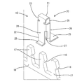
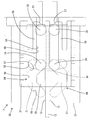
- FIG. 1 is an exploded perspective view of a male connector constituting the card edge connector of the first embodiment.
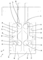
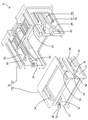
- FIG. 2 is an exploded perspective view of the female side connector constituting the card edge connector.
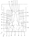
- FIG. 3 is an exploded perspective view of the terminal module mounted on the circuit board.
- FIG. 4 is a cross-sectional view of the circuit board.
- FIG. 5 is a cross-sectional view taken along line XX of FIG.
- FIG. 6 is a side view showing a state in which the terminal fitting is attached to the housing of the female connector.
- FIG. 7 is a side sectional view showing a state in which the terminal fitting is attached to the housing of the female connector.
- FIG. 8 is a side view showing a state in which the first housing and the terminal fitting are displaced to non-contact positions.
- FIG. 1 is an exploded perspective view of a male connector constituting the card edge connector of the first embodiment.
- FIG. 2 is an exploded perspective view of the female side connector constituting the card edge connector.
- FIG. 9 is a side sectional view showing a state in which the first housing and the terminal fitting are displaced to non-contact positions.
- FIG. 10 is a side view showing a state in which the terminal fitting is displaced to the contact position and connected to the substrate side terminal.
- FIG. 11 is a side sectional view showing a state in which the terminal fitting is displaced to the contact position and connected to the substrate side terminal.
- FIG. 12 is a perspective view showing a state in which the second housing and the third housing are assembled in the second embodiment.
- FIG. 13 is a perspective view showing a state in which the second housing and the third housing are separated.
- FIG. 14 is a perspective view of the circuit board.
- FIG. 15 is a plan sectional view showing a state in which the elastic locking piece of the second housing is locked to the circuit board.
- FIG. 16 is a plan sectional view showing a state in which the second elastic locking piece of the second housing and the third elastic locking piece of the third housing are locked to the circuit board.
- the card edge connector of the first disclosure is (1) A housing, a terminal fitting attached to the housing, and a circuit board having a mounting surface and being fitted to the housing in parallel with the mounting surface are provided. A substrate-side terminal in a form protruding from the mounting surface is provided, and a recess for accommodating the substrate-side terminal is formed in the terminal fitting, and an elastic contact piece provided in the recess serves with respect to the substrate-side terminal. Contact elastically. According to the configuration of the present disclosure, when the elastic contact piece elastically contacts the substrate side terminal, the terminal fitting receives the reaction force from the substrate side terminal. Even if the housing is thermally deformed or the thickness of the circuit board varies, the contact pressure between the terminal fittings and the terminals on the board side is stable.
- the terminal fitting is supported so as to be able to swing between a connection position close to the mounting surface and a non-connection position separated from the mounting surface with the shaft portion as a fulcrum, and the terminal fitting is supported.
- the elastic contact piece is in the connection position, the elastic contact piece is in contact with the substrate side terminal, and when the terminal fitting is in the non-connection position, the elastic contact piece is not in contact with the substrate side terminal.
- the terminal fitting is displaced in the direction of approaching or separating from the mounting surface. There is a need. If an attempt is made to translate the terminal fitting in a direction orthogonal to the mounting surface, the structure for guiding the terminal fitting becomes complicated. In the present disclosure, since the terminal fitting is made to swing, the structure for guiding the terminal fitting can be simplified.
- the housing has a first housing for holding the terminal fitting and a stopper with which the insertion end of the circuit board abuts, and the first housing is connected with the shaft as a fulcrum.
- a second housing that holds the second housing so that it can swing between a position and a non-connecting position, and a third housing that can be displaced relative to the second housing in parallel with the mating direction of the housing and the circuit board.
- the first housing and the second housing are restricted from being displaced in a direction parallel to the fitting direction of the housing and the circuit board, and the third housing includes the second housing and the circuit board. It is preferable that a guide portion is formed to displace the first housing between the connection position and the non-connection position in accordance with the relative displacement with the third housing.
- the terminal fitting is displaced from the non-connection position to the connection position and brought into contact with the terminal on the substrate side, it is conceivable to swing the terminal fitting from the non-connection position to the connection position while inserting the circuit board into the housing. ..
- the circuit board and the terminal fitting are displaced relative to each other in two different directions, the relative displacement path of the elastic contact piece with respect to the terminal on the board side becomes unstable, and the elastic contact piece is on the board side. It may interfere with the terminals.
- the terminal fitting is oscillated with the shaft portion as a fulcrum in a state where the circuit board is abutted against the stopper of the second housing.
- the shaft portion is not displaced relative to the stopper in the front-rear direction, the relative displacement path of the elastic contact piece with respect to the substrate side terminal is stable. As a result, the elastic contact piece and the substrate side terminal can be connected without interfering with each other.
- the second housing is elastically deformed in the process of assembling the first housing to the second housing, and the first housing is elastically held in the assembled state with respect to the second housing. It is preferable that the holding piece is formed. According to this configuration, the work of assembling the first housing to the second housing is easy.
- the second housing is formed with a guide groove along the swing path of the first housing, and the first housing is formed with a guide pin and a shaft portion to form the guide. It is preferable that the pin can be slidably contacted with respect to the guide groove from the rear, and the shaft portion is locked from the front with respect to the elastic holding piece. According to this configuration, the first housing can be held in a state of being positioned in the front-rear direction with respect to the second housing without forming a circular bearing hole in the second housing.
- a second locking portion and a third locking portion are formed on the circuit board, and in the second locking portion, the circuit board abuts on the stopper.
- the second elastic locking piece of the second housing is elastically locked
- the third locking portion is the first in a state where the first housing is displaced to the connection position. 3 It is preferable that the third elastic locking piece of the housing is elastically locked.
- the second housing and the third housing individually rattle with respect to the circuit board.
- the second housing and the third housing are individually and elastically locked to the circuit board, the second housing rattles with respect to the circuit board and the third housing with respect to the circuit board. It is possible to prevent the housing from rattling.
- the plurality of the substrate-side terminals are arranged so as to be arranged in a row, and the recesses may penetrate in the same direction as the arrangement direction of the substrate-side terminals. preferable. According to this configuration, it is possible to absorb the misalignment between the board-side terminals and the terminal fittings in the arrangement direction of the board-side terminals.
- an electric wire is connected to the rear end portion of the terminal fitting, and the elastic contact piece is arranged along the inner surface on the front side of the recess. .. According to this configuration, when the electric wire is pulled backward, the elastic contact piece is elastically deformed, so that the load on the terminal on the substrate side is reduced.
- the contact portion of the elastic contact piece is arranged in a region closer to the mounting surface than the center of the elastic contact piece in the protruding direction of the substrate side terminal. Is preferable. According to this configuration, the contact position between the board-side terminal and the contact portion of the elastic contact piece is close to the mounting surface, so that the protrusion dimension of the board-side terminal from the mounting surface can be reduced.
- the circuit board of the second disclosure is (10) In a state where the mounting surface and a plurality of board-side terminals protruding from the mounting surface are fitted in parallel with the mounting surface with respect to the housing, the terminal fittings attached to the housing are It comes into contact with the substrate side terminals, has a plurality of support portions on the mounting surface, and mounts a mounting member made of a single component, and the plurality of substrate sides are mounted on the plurality of support portions. It is preferable that the terminals are individually assembled. When a plurality of board-side terminals are individually mounted on a circuit board, the number of mounting steps on the circuit board increases.
- the mounting process on the mounting surface can be performed with one action. Therefore, the manufacturing cost of the circuit board can be reduced.
- the support portion is formed with a retaining portion for preventing the substrate-side terminal from coming off by locking the substrate-side terminal, and the substrate-side terminal and the retaining portion are connected to each other. It is preferable that a clearance in a direction parallel to the direction in which the substrate-side terminal protrudes from the mounting surface is secured between them.
- the assembly position of the substrate-side terminal in the support portion may vary depending on the dimensional tolerance of the support portion and the substrate-side terminal. If there are variations in the assembly positions of the board-side terminals on the support portion, there is a concern that the board-side terminals may not be in contact with the mounting surface.
- a clearance is provided between the retaining portion of the support portion and the board-side terminal in the direction in which the board-side terminal protrudes from the mounting surface. Therefore, if the mounting surface is arranged horizontally, the board-side terminal can be provided. It can be reliably brought into contact with the mounting surface by its own weight.
- the substrate side terminal is located on the side opposite to the mounting surface with the substrate contact portion fixed to the mounting surface by solder and the substrate contact portion sandwiched between them.
- the terminal fitting is located and has a terminal contact portion for contacting an elastic contact piece of the terminal fitting, the substrate contact portion is parallel to the mounting surface of the circuit board, and the terminal fitting in the terminal contact portion. It is preferable that a seating surface portion protruding toward the contact surface side with the surface is formed. According to this configuration, the contact area of the solder with respect to the contact portion for the substrate remains within the range of the thickness of the seat surface portion. Therefore, there is no possibility that the solder will wet and spread to the contact surface with the terminal fitting at the terminal contact portion.
- the substrate side terminal is formed with a curved surface portion along the displacement path of the terminal fitting that swings with the shaft portion as a fulcrum, and the curved surface portion is formed with the terminal. It is preferable that the elastic contact pieces of the metal fittings are in sliding contact with each other in an elastically deformed state. According to this configuration, the amount of elastic displacement of the elastic contact piece with respect to the terminal on the substrate side is stabilized during the swinging process of the terminal fitting, so that the resistance when swinging the terminal fitting is stable.
- Example 1 embodying the card edge connector A of the present disclosure will be described with reference to FIGS. 1 to 11. It should be noted that the present invention is not limited to these examples, and is indicated by the scope of claims, and is intended to include all modifications within the meaning and scope equivalent to the scope of claims.
- the card edge connector A of the first embodiment has a male side connector M and a female side connector F.
- the male side connector M and the female side connector F are fitted by approaching each other in the front-rear direction while facing each other.
- the diagonally lower right in FIG. 1 and the right in FIGS. 9 to 11 are defined as the front.
- the front-rear direction of the female connector F the diagonally upper left side in FIG. 2 and the left side in FIGS. 6 to 11 are defined as the front.
- the front-rear direction and the mating direction of the male side connector M (circuit board 12) and the female side connector F are used synonymously.
- the directions appearing in FIGS. 1 to 11 are defined as upward and downward as they are.
- the male side connector M is configured by assembling the circuit board 12 to the hood-shaped male side housing 10.
- a lock hole 11 is formed in the male side housing 10.
- the front surface (upper surface in FIGS. 1, 3 to 5) and the back surface (lower surface in FIGS. 1, 3 to 5) of the circuit board 12 are mounting surfaces 13 on which a printed circuit (not shown) is formed.
- the edge portion of the outer peripheral edge portion of the circuit board 12 that fits with the female connector F is the insertion end portion 14.
- the insertion end portion 14 is housed in the male side housing 10.
- the direction orthogonal to the circuit board 12 and the mounting surface 13 and the vertical direction are used interchangeably.
- the terminal module 15 is mounted on the insertion end 14 of both the front and back mounting surfaces 13.
- the terminal module 15 is configured by assembling one mounting member 16 and a plurality of board-side terminals 20.
- the mounting member 16 is a single component made of synthetic resin, and has an elongated shape in the width direction along the insertion end portion 14.
- a plurality of support portions 17 projecting in a direction away from the mounting surface 13 are integrally formed on the mounting member 16 so as to be lined up at a constant pitch in the left-right direction.
- a protrusion-shaped retaining portion 18 is formed on one of the left and right side surfaces of the support portion 17.
- the substrate side terminal 20 is formed by bending a metal plate material.
- the board-side terminal 20 is a single component having a vertically long box portion 21 opened so as to face the mounting surface 13, two front and rear seat surface portions 25, and a hook portion 27. Is.
- the end of the box portion 21 on the side closer to the mounting surface 13 is the substrate contact portion 22 fixed to the mounting surface 13 by the solder S.
- the region of the box portion 21 on the side opposite to the mounting surface 13 with the substrate contact portion 22 interposed therebetween is a terminal contact portion 23 for contacting the elastic contact piece 44 of the terminal fitting 40.
- a front seating surface portion 25 is formed in a portion of the substrate contact portion 22 that constitutes the front plate portion 24 of the box portion 21.
- the seat surface portion 25 on the front side projects forward from the front plate portion 24 so as to be parallel to the mounting surface 13.
- a rear seating surface portion 25 is formed at a portion of the substrate contact portion 22 that constitutes the rear plate portion 26 of the box portion 21.
- the seat surface portion 25 on the rear side projects rearward from the rear plate portion 26 so as to be parallel to the mounting surface 13.
- the hook portion 27 projects diagonally from the edge of one of the left and right side plate portions constituting the box portion 21 on the open surface side into the inside of the box portion 21.
- a curved surface portion 28 is formed on the terminal contact portion 23.
- the curved surface portion 28 is formed at an end portion of the rear plate portion 26 constituting the box portion 21 on the side opposite to the open end, and forms an arc shape when the substrate side terminal 20 is viewed from the side.
- the curved surface portion 28 has a shape along a displacement path of the terminal fitting 40 described later.
- a contact surface 29 is formed on the terminal contact portion 23.
- the contact surface 29 is formed in a region of the outer surface of the rear plate portion 26 that is closer to the mounting surface 13 than the curved surface portion 28, and the elastic contact piece 44 of the terminal fitting 40 described later is elastically contacted.
- the substrate side terminal 20 is assembled so as to cover the support portion 17 with the box portion 21.
- a clearance C is secured between the protruding end portion of the hook portion 27 and the retaining portion 18, so that the board side terminal 20 is attached to the support portion 17 with respect to the support portion 17. It can be displaced relative to the mounting surface 13 in a direction perpendicular to it.
- the board-side terminal 20 is displaced in a direction away from the mounting surface 13, the protruding end of the hooking portion 27 abuts on the hooking portion 27, so that the board-side terminal 20 does not separate from the support portion 17.
- the terminal module 15 is mounted on the mounting surface 13 in a state where a plurality of board-side terminals 20 are individually assembled to the plurality of support portions 17.
- the mounting member 16 is fixed to the mounting surface 13 by welding.
- Both the front and rear seat surface portions 25 are electrically conductively fixed to the printed circuit (not shown) of the mounting surface 13 by the solder S. Since the board-side terminal 20 is not fixed to the support portion 17 and can be displaced relative to the support portion 17, the seat surface portion 25 can be reliably fixed to the mounting surface 13.
- solder S does not contact the front plate portion 24 and the rear plate portion 26 perpendicular to the mounting surface 13 but only the seat surface portion 25, the solder S does not wet and spread to the contact surface 29 of the front plate portion 24.
- a plurality of board-side terminals 20 are mounted on the insertion end portions 14 of the front and back mounting surfaces 13 so as to be arranged in a row in the left-right direction at a constant pitch via the mounting members 16.
- the female side connector F includes a female side housing 30 and a plurality of terminal fittings 40.
- the female side housing 30 includes a pair of first housings 31 that are vertically symmetrical with respect to the circuit board 12, a plurality of terminal fittings 40, one second housing 32, and one third housing 33. ing.
- the first housing 31 is made of synthetic resin and has a flat rectangular shape parallel to the mounting surface 13.
- a cylindrical guide pin 34 whose axis is directed in the left-right direction and a cylindrical shaft portion 35 whose axis is directed in the left-right direction are formed. Has been done.
- the guide pin 34 is located at the front end of the first housing 31.
- the shaft portion 35 is located at the rear end portion of the first housing 31.
- a plurality of terminal accommodating chambers 36 elongated in the front-rear direction are formed in the first housing 31 in a state of being arranged in a row in the left-right direction.
- the first housing 31 is formed with a plurality of openings 37 that open to the front end surface of the first housing 31 and individually communicate with the front ends of the plurality of terminal accommodating chambers 36.
- an expansion portion 38 in a form that expands toward the front end surface side of the first housing 31 is formed.
- a terminal fitting 40 fixed to the front end portion of the electric wire 46 is accommodated.
- the terminal fitting 40 housed in the terminal storage chamber 36 is held out by a retainer 47 attached to the first housing 31.
- the electric wire 46 is led out from the rear end of the first housing 31 to the rear.
- the terminal fitting 40 is a single component having a terminal body portion 41 and a crimping portion 42.
- the terminal body 41 constitutes the front end of the terminal fitting 40.
- a recess 43 and an elastic contact piece 44 are formed in the terminal body 41.
- the recess 43 is open to the surface of the terminal body 41 facing the mounting surface 13 and the left and right side surfaces of the terminal body 41.
- the elastic contact piece 44 is arranged along the inner surface on the front side of the inner surface of the recess 43.
- the contact portion 45 of the elastic contact piece 44 is located in a region closer to the mounting surface 13 than the center of the elastic contact piece 44 in the direction orthogonal to the mounting surface 13.
- the crimping portion 42 is located at the rear end of the terminal fitting 40.
- the crimping portion 42 is crimped to the electric wire 46.
- the second housing 32 is a single part made of synthetic resin, and has a symmetrical shape. As shown in FIG. 2, the second housing 32 has a pair of side surface portions 50, a pair of front side connecting portions 51, a pair of rear side connecting portions 52, and a stopper 53.
- the front connecting portion 51 connects the front end portions at the upper and lower end edges of the side surface portion 50 to each other.
- the rear connecting portion 52 connects the rear end portions at the upper and lower end edges of the side surface portion 50.
- the stopper 53 has a flat plate shape parallel to the mounting surface 13, and connects the centers of the left and right side surface portions 50 in the vertical direction.
- a pair of vertically symmetrical slide grooves 54 are formed on the left and right side surface portions 50, respectively.
- the slide groove 54 extends linearly in the front-rear direction, that is, in the direction parallel to the fitting direction of the circuit board 12 and the female connector F.
- a pair of vertically symmetrical guide grooves 55 are formed on the left and right side surface portions 50, respectively.
- the guide groove 55 is connected to the front end of the slide groove 54, and extends so as to be separated from each other in the vertical direction and in an arc shape.
- a pair of vertically symmetrical elastic holding pieces 56 are formed on the left and right side surface portions 50, respectively.
- the elastic holding piece 56 has a form that extends rearward along the slide groove 54 in a cantilever shape.
- the elastic holding pieces 56 can be elastically deformed in the vertical direction so as to be separated from each other.
- a holding protrusion 57 is formed at the rear end portion (extending end portion) of the elastic holding piece 56.
- the holding protrusion 57 constitutes the rear end portion of the slide groove 54.
- the rear end of the slide groove 54 is open to the rear outside of the second housing 32.
- the third housing 33 is a single part made of synthetic resin, and has a symmetrical shape. As shown in FIG. 2, the third housing 33 has a frame portion 60, a pair of vertically symmetrical support wall portions 61, and a pair of symmetrical side wall portions 62.
- the frame portion 60 is arranged at the rear end portion of the third housing 33, and has a rectangular shape when the third housing 33 is viewed from the rear.
- the pair of support wall portions 61 project forward from both the upper and lower edges of the frame portion 60.
- a lock arm 63 is formed on one of the support wall portions 61.
- the pair of side wall portions 62 are in a form of protruding forward from the left and right side edges of the frame portion 60.
- the left and right side edges of the support wall portion 61 are connected at right angles to the upper edge portion or the lower edge portion of the left and right side wall portions 62.
- a pair of vertically symmetrical guide portions 64 are formed on the left and right side wall portions 62, respectively.
- the guide portion 64 has a slit shape extending in the front-rear direction as a whole.
- the guide portion 64 has a form in which the first guide 65, the second guide 66, the third guide 67, and the fourth guide 68 are connected in order from the front end to the rear end.
- the pair of vertically symmetrical first guides 65 are inclined so as to be separated from each other from the front end to the rear end in the front-rear direction.
- the pair of vertically symmetrical second guides 66 are parallel to the front-rear direction.
- the pair of vertically symmetrical third guides 67 are inclined so as to approach each other from the front end to the rear end in the front-rear direction.
- the pair of vertically symmetrical fourth guides 68 are parallel to the front-rear direction.
- the rear end of the fourth guide 68 is open to the rear end surface of the third housing 33.
- Assembling the female connector F is performed by the following procedure. First, both the upper and lower first housings 31 are assembled from the rear to the third housing 33, and the guide pin 34 and the shaft portion 35 are fitted into the guide portion 64. As the assembly of the first housing 31 progresses, the guide pin 34 comes into sliding contact with the fourth guide 68, the third guide 67, the second guide 66, and the first guide 65 in this order.
- the second housing 32 is assembled from the front to the first housing 31 and the third housing 33.
- the holding protrusion 57 interferes with the guide pin 34 to elastically deform the elastic holding piece 56, and the guide pin 34 fits into the rear end portion of the slide groove 54.
- the holding protrusion 57 interferes with the shaft portion 35, so that the elastic holding piece 56 is elastically deformed.
- FIG. 6 when the elastic holding piece 56 is elastically restored and the shaft portion 35 is fitted to the rear end portion of the slide groove 54, the second housing 32 is assembled to the first housing 31 and the third housing 33. Is completed.
- the guide pin 34 abuts or approaches the front end of the slide groove 54 from the rear, and the shaft portion 35 faces the rear end of the slide groove 54 ( It abuts or approaches the holding protrusion 57) from the front and faces it.
- the guide pin 34 and the shaft portion 35 are sandwiched between the front end and the rear end of the slide groove 54 in the front-rear direction, so that the first housing 31 and the second housing 32 are restricted from being displaced in the front-rear direction. It can be assembled with.
- the second housing 32 and the third housing 33 can be relatively displaced in the front-rear direction. As the second housing 32 and the third housing 33 are displaced relative to each other in the front-rear direction, the guide pin 34 slides between the first guide 65 and the fourth guide 68, and the shaft portion 35 moves to the fourth guide 68. It slides in the front-back direction. Since the front end of the slide groove 54 communicates with the guide groove 55 in the vertical direction, the first housing 31 uses the shaft portion 35 as a fulcrum with respect to the second housing 32 while moving the guide pin 34 in the guide groove 55. It is possible to swing in the vertical direction.
- the upper and lower first housings 31 are displaced from each other in advance to non-connected positions (see FIGS. 8 and 9). Specifically, the third housing 33 is displaced forward relative to the first housing 31 and the second housing 32 from the state where the guide pin 34 is located at the front end of the first guide 65.
- the guide pin 34 is in sliding contact with the first guide 65, the first housing 31 swings so as to be separated from each other with the shaft portion 35 as a fulcrum, and is displaced to the non-connection position.
- the guide pin 34 enters the second guide 66 the second housing 32 and the third housing 33 are held so as not to be misaligned.
- the circuit board 12 When the first housing 31 is held in the non-connected position, as shown in FIG. 9, the circuit board 12 is inserted between the upper and lower first housings 31 without causing the substrate side terminal 20 to interfere with the first housing 31.
- An insertion space 69 that can be inserted is secured.
- the male side housing 10 and the third housing 33 are grasped, the male side connector M and the female side connector F are started to be fitted, and the insertion end portion 14 of the circuit board 12 is inserted as shown in FIG. It is inserted into the space 69 and abuts against the front end of the stopper 53.
- the recess 43 of the terminal fitting 40 faces the substrate side terminal 20 in the vertical direction.
- the third housing 33 is displaced forward relative to the second housing 32. Therefore, the guide pin 34 shifts from the second guide 66 to the third guide 67. Since the third guide 67 is inclined with respect to the front-rear direction, the guide pins 34 are in sliding contact with the third guide 67, so that the upper and lower first housings 31 at the non-connected positions come close to each other. The guide pin 34 moves in the guide groove 55 of the second housing 32 while sliding in contact with the third guide 67. As shown in FIG. 10, when the guide pin 34 reaches the fourth guide 68, the first housing 31 reaches the connection position (see FIGS. 10 and 11).
- the recess 43 of the terminal fitting 40 fits with the substrate side terminal 20, and the elastic contact piece 44 comes into contact with the substrate side terminal 20.
- the elastic contact piece 44 is in sliding contact with the curved surface portion 28 of the substrate side terminal 20 in a state of being elastically deformed. Since the curved surface portion 28 has an arc shape centered on the shaft portion 35 of the first housing 31, the amount of elastic deformation of the elastic contact piece 44 is kept constant while the elastic contact piece 44 is in sliding contact with the curved surface portion 28. Is done.
- the contact portion 45 of the elastic contact piece 44 is in a state of elastic contact with the contact surface 29. Since the outer surface of the curved surface portion 28 and the contact surface 29 are smoothly connected to each other, the amount of elastic deformation of the elastic contact piece 44 does not fluctuate when the elastic contact piece 44 moves from the curved surface portion 28 to the contact surface 29.
- the contact portion 45 on the back of the cross section reaches the contact surface 29, the fitting of the male side connector M and the female side connector F is completed.
- both connectors F and M are fitted, the lock arm 63 of the third housing 33 is locked in the lock hole 11 of the male housing 10, so that both connectors F and M are locked in the fitted state.
- the elastic contact piece 44 elastically presses the board side terminal 20 from the front, and the board side terminal 20 is pressed against the rear inner surface of the recess 43.
- the elastic contact piece 44 is elastically deformed, so that the terminal fitting 40 is displaced relative to the substrate side terminal 20, so that the load on the substrate side terminal 20 is reduced.
- a tapered portion 39 in a form in which a region facing the stopper 53 of the second housing 32 is cut out is formed at the rear end portion of the first housing 31.
- the first housing 31 is formed with an opening 37 that opens at the front end surface of the first housing 31 and communicates with the terminal accommodating chamber 36.
- the opening 37 is provided with an expanding portion 38 that expands toward the front end surface of the first housing 31.
- the lock arm 63 is unlocked to unlock the lock arm 63 and the lock hole 11, and the third housing 33 is disconnected from the male connector M. Pull in the direction of detachment. Then, the guide pin 34 is in sliding contact with the third guide 67, so that the first housing 31 is displaced from the connected position to the non-connected position side. When the guide pin 34 reaches the second guide 66, the recess 43 of the terminal fitting 40 comes off from the substrate side terminal 20. After that, the third housing 33 and the second housing 32 may be moved integrally and separated from the male housing 10.
- the card edge connector A of the first embodiment has a female side housing 30, a terminal fitting 40 attached to the female side housing 30, and a circuit board 12.
- the circuit board 12 has a mounting surface 13 and is fitted to the female side housing 30 in parallel with the mounting surface 13.
- the circuit board 12 is provided with a plurality of board-side terminals 20 in a form protruding from the mounting surface 13.
- the terminal fitting 40 is opened so as to face the mounting surface 13 and is formed with a recess 43 for accommodating the substrate-side terminal 20.
- the elastic contact piece 44 provided in the recess 43 elastically contacts the substrate side terminal 20. According to the above configuration, when the elastic contact piece 44 elastically contacts the substrate side terminal 20, the terminal fitting 40 receives the reaction force from the substrate side terminal 20. Even if the housing is thermally deformed or the thickness of the circuit board 12 varies, the contact pressure between the terminal fitting 40 and the board-side terminal 20 is stable.
- the terminal fitting 40 In order to fit the recess 43 of the terminal fitting 40 into contact with the elastic contact piece 44 with respect to the substrate side terminal 20 protruding from the mounting surface 13 of the circuit board 12, the terminal fitting 40 is attached to the mounting surface 13. It is necessary to displace in the direction of approaching and separating. If the terminal fitting 40 is to be translated in the direction orthogonal to the mounting surface 13, the structure for guiding the terminal fitting 40 becomes complicated.
- the terminal fitting 40 is supported by the female side housing 30 so as to be able to swing with the shaft portion 35 as a fulcrum.
- the terminal fitting 40 swings between a connection position close to the mounting surface 13 and a non-connection position separated from the mounting surface 13.
- the elastic contact piece 44 comes into contact with the substrate side terminal 20.
- the elastic contact piece 44 is in non-contact with the substrate side terminal 20. Since the card edge connector A of the first embodiment swings the terminal fitting 40, the structure for guiding the terminal fitting 40 can be simplified.
- the terminal fitting 40 is moved from the non-connection position to the connection position while the circuit board 12 is inserted into the female side housing 30. It is conceivable to swing. However, in this case, since the circuit board 12 and the terminal fitting 40 are displaced relative to each other in two different directions, the relative displacement path of the elastic contact piece 44 with respect to the substrate side terminal 20 becomes unstable, resulting in elastic contact. The piece 44 may interfere with the substrate side terminal 20.
- the female side housing 30 of the first embodiment is configured to include a first housing 31 for holding the terminal fitting 40, a second housing 32, and a third housing 33.
- the second housing 32 has a stopper 53 with which the insertion end portion 14 of the circuit board 12 abuts.
- the first housing 31 and the second housing 32 are restricted from being displaced in a direction parallel to the mating direction of the female housing 30 and the circuit board 12.
- the second housing 32 holds the first housing 31 so as to be able to swing between the connected position and the non-connected position with the shaft portion 35 as a fulcrum.
- the third housing 33 may be displaced relative to the second housing 32 in parallel with the fitting direction of the female housing 30 and the circuit board 12.
- the third housing 33 is formed with a guide portion 64 that displaces the first housing 31 between the connected position and the non-connected position due to the relative displacement between the second housing 32 and the third housing 33.
- the terminal fitting 40 is swung around the shaft portion 35 as a fulcrum in a state where the insertion end portion 14 of the circuit board 12 is abutted against the stopper 53 of the second housing 32. Since the shaft portion 35 is not displaced relative to the stopper 53 in the front-rear direction, the relative displacement path of the elastic contact piece 44 with respect to the substrate side terminal 20 is stable. As a result, the elastic contact piece 44 and the substrate side terminal 20 can be connected without interfering with each other.
- the second housing 32 is formed with an elastic holding piece 56 that is elastically deformed in the process of assembling the first housing 31 to the second housing 32 and holds the first housing 31 in the assembled state with respect to the second housing 32. .. According to this configuration, the work of assembling the first housing 31 to the second housing 32 is easy.
- the second housing 32 is formed with a guide groove 55 along the swing path of the first housing 31.
- a guide pin 34 and a shaft portion 35 are formed in the first housing 31.
- the guide pin 34 can be slidably contacted with the guide groove 55 from behind.
- the shaft portion 35 is locked to the elastic holding piece 56 from the front. According to this configuration, the first housing 31 can be held in a state of being positioned in the front-rear direction with respect to the second housing 32 without forming a circular bearing hole in the second housing 32.
- the plurality of board-side terminals 20 are arranged so as to be lined up along the insertion end portion 14 of the mounting surface 13.
- the recess 43 has a form of penetrating in the same direction as the arrangement direction of the substrate side terminals 20. According to this configuration, it is possible to absorb the misalignment between the board-side terminals 20 and the terminal fittings 40 in the arrangement direction of the board-side terminals 20.
- An electric wire 46 is connected to the rear end of the terminal fitting 40.
- the elastic contact piece 44 is arranged along the inner surface on the front side of the recess 43. According to this configuration, when the electric wire 46 is pulled backward, the elastic contact piece 44 is elastically deformed, so that the load on the substrate side terminal 20 is reduced.
- the contact portion 45 of the elastic contact piece 44 is arranged in a region closer to the mounting surface 13 than the center of the elastic contact piece 44 in the protruding direction of the substrate side terminal 20. According to this configuration, the contact position between the board-side terminal 20 and the contact portion 45 of the elastic contact piece 44 is close to the mounting surface 13, so that the protrusion dimension of the board-side terminal 20 from the mounting surface 13 can be reduced. can.
- the circuit board 12 of the first embodiment has a mounting surface 13 and a plurality of board-side terminals 20 in a form protruding from the mounting surface 13.
- the terminal fitting 40 attached to the female housing 30 comes into contact with the board terminal 20.
- a plurality of board-side terminals 20 are individually mounted on the circuit board 12, the number of mounting steps on the circuit board 12 is increased.
- a mounting member 16 having a plurality of support portions 17 and being composed of a single component is mounted on the mounting surface 13.
- a plurality of substrate-side terminals 20 are individually assembled to the plurality of support portions 17. According to this configuration, after assembling the plurality of board-side terminals 20 to the plurality of support portions 17, the mounting member 16 may be mounted on the mounting surface 13, so that the mounting process on the mounting surface 13 can be performed with one action.
- the assembly position of the substrate-side terminal 20 on the support portion 17 may vary depending on the dimensional tolerance of the support portion 17 and the substrate-side terminal 20. If there are variations in the assembly positions of the board-side terminals 20 on the support portion 17, there is a concern that the board-side terminals 20 may not be in contact with the mounting surface 13.
- the circuit board 12 of the first embodiment has a retaining portion 18 formed on the support portion 17. The retaining portion 18 prevents the substrate-side terminal 20 from coming off by locking the hooking portion 27 of the substrate-side terminal 20.
- a clearance C is secured between the hooking portion 27 and the retaining portion 18 in a direction parallel to the direction in which the substrate side terminal 20 protrudes from the mounting surface 13. Since a clearance C is provided between the retaining portion 18 of the support portion 17 and the board-side terminal 20, if the mounting surface 13 is arranged horizontally, the board-side terminal 20 can be reliably brought into contact with the mounting surface 13 by its own weight. can.
- the board-side terminal 20 has a board contact portion 22 fixed to the mounting surface 13 by solder S, and a terminal contact portion 23.
- the terminal contact portion 23 is located on the side opposite to the mounting surface 13 with the substrate contact portion 22 interposed therebetween.
- the elastic contact piece 44 of the terminal fitting 40 comes into contact with the terminal contact portion 23.
- the board contact portion 22 is formed with a seat surface portion 25 that is parallel to the mounting surface 13 of the circuit board 12 and projects toward the contact surface 29 side of the terminal contact portion 23 with the terminal fitting 40.
- the substrate side terminal 20 is formed with a curved surface portion 28 along the displacement path of the terminal fitting 40 that swings around the shaft portion 35 as a fulcrum.
- the elastic contact piece 44 of the terminal fitting 40 is in sliding contact with the curved surface portion 28 in a state of being elastically deformed. According to this configuration, the amount of elastic displacement of the elastic contact piece 44 with respect to the substrate side terminal 20 is stabilized in the swinging process of the terminal fitting 40, so that the resistance when swinging the terminal fitting 40 is stable.
- Example 2 embodying the card edge connector B of the present disclosure will be described with reference to FIGS. 12 to 16.
- the card edge connector B of the second embodiment is provided with a locking structure between the circuit board 70 and the female housing 75. Since other configurations are the same as those in the first embodiment, the same configurations are designated by the same reference numerals, and the description of the structure, action, and effect will be omitted.
- a pair of symmetrical second locking portions 72 and a pair of symmetrical third locking portions 73 are formed at the insertion end portion 71 of the circuit board 70.
- the second locking portion 72 is slightly rearward of the substrate side terminal 20 (terminal module 15) of the left and right side edges of the insertion end portion 71 (the side opposite to the fitting direction of the circuit board 70 with respect to the female side housing 75). ) Is recessed.
- the third locking portion 73 has a shape in which a portion of the left and right side edges of the insertion end portion 71 that is slightly rearward of the second locking portion 72 is projected.
- a pair of second elastic locking pieces 78 are formed on the left and right side surface portions 77 of the second housing 76.
- the second elastic locking piece 78 is located at the front end portion of the side surface portion 77, and extends forward (in the same direction as the fitting direction of the female side housing 75 with respect to the circuit board 70) in a cantilever shape.
- Both the left and right second elastic locking pieces 78 are formed with a second locking projection 79 in a form protruding toward the inner surface side (the second elastic locking piece 78 side on the mating side).
- Both the left and right second elastic locking pieces 78 are formed with a pressure receiving portion 80 protruding toward the outer surface side (the side opposite to the second elastic locking piece 78 on the mating side).
- a pair of third elastic locking pieces 83 are formed on the left and right side wall portions 82 of the third housing 81.
- the third elastic locking piece 83 is located at the front end portion of the side wall portion 82 and extends forward in a cantilever shape.
- the left and right third elastic locking pieces 83 have a third locking projection 84 protruding toward the inner surface side (the third elastic locking piece 83 side on the mating side) and a pressing portion 85 protruding toward the inner surface side. Is formed.
- the guide portion 86 formed on the side wall portion 82 of the third housing 81 does not have the first guide unlike the guide portion 64 of the first embodiment. That is, the guide unit 86 of the second embodiment is composed of the second guide 66, the third guide 67, and the fourth guide 68 in the first embodiment.
- the third housing 81 When fitting the female side housing 75 and the circuit board 70, the third housing 81 is grasped and pushed so as to approach the circuit board 70. When the third housing 81 is pushed and moved, the pressing portion 85 pushes the pressure receiving portion 80, so that the second housing 76 moves integrally with the third housing 81 and approaches the circuit board 70.
- the second locking projection 79 fits with the second locking portion 72, and the circuit board 70 and the second 2 Lock the housing 76 so that it cannot be detached.
- the third locking projection 84 rides on the third locking portion 73, the third elastic locking piece 83 is elastically deformed so as to separate the pressing portion 85 from the pressure receiving portion 80.
- the third housing 81 moves relative to the circuit board 70 and the second housing 76.
- the guide pin (not shown) of the first housing 31 (not shown) fitted to the second guide 66 slides into contact with the third guide 67.
- the inclination of the third guide 67 causes the first housing 31 to swing from the non-connected position to the connected position.
- the terminal fitting 40 (not shown) and the board-side terminal 20 are connected.
- the third elastic locking piece 83 elastically returns and the third locking projection 84 is locked to the third locking portion 73. By this locking, the female side housing 75 and the circuit board 70 are held in the fitted state.
- the circuit board 70 of the second embodiment is formed with a second locking portion 72 and a third locking portion 73.
- the second locking portion 72 elastically locks the second elastic locking piece 78 of the second housing 76 in a state where the circuit board 70 abuts on the stopper 53.
- the third locking portion 73 elastically locks the third elastic locking piece 83 of the third housing 81 in a state where the first housing 31 is displaced to the connection position.
- the second housing 76 and the third housing 81 individually rattle with respect to the circuit board 70.
- the second housing 76 and the third housing 81 are individually and elastically locked to the circuit board 70, so that the second housing 76 rattles with respect to the circuit board 70. It is possible to prevent the third housing 81 from rattling with respect to the circuit board 70.
- the present invention is not limited to the examples described in the above description and drawings, but is shown by the scope of claims.
- the present invention includes the meaning equivalent to the scope of claims and all modifications within the scope of claims, and is intended to include the following embodiments.
- the terminal fitting and the first housing swing, but the terminal fitting and the first housing may be translated.
- the first housing is formed with a tapered portion for avoiding interference with the second housing, but the first housing may not have such a tapered portion.
- the second housing holds the first housing by the elastic holding piece, but the first housing is held by fitting the shaft portion of the first housing into the bearing hole formed in the second housing. You may.
- the concave portion penetrates in the arrangement direction of the substrate side terminals, but the concave portion may surround the substrate side terminal over the entire circumference.
- the elastic contact piece is arranged along the front wall portion of the recess, but the elastic contact piece may be arranged along the rear wall surface of the recess.
- the plurality of board-side terminals are mounted on the mounting surface via one mounting member, but the plurality of board-side terminals may be individually mounted on the mounting surface.
- the substrate-side terminals are assembled so as to be relatively displaced with respect to the support portion, but the substrate-side terminals may be fixed to the support portion.
- Crimping part 43 Recessed portion 44 ... Elastic contact piece 45 ... Contact part 46 ... Electric wire 47 ... Retainer 50 ... Side part 51 ... Front side connecting part 52 ... Rear side connecting part 53 ... Stopper 54 ... Slide groove 55 ... Guide groove 56 ... Elastic holding piece 57 ... Holding protrusion 60 ... Frame part 61 ... Support wall part 62 ... Side wall part 63 ... Lock arm 64 ... Guide part 65 ... First guide 66 ... Second guide 67 ... Third guide 68 ... Fourth guide 69 ... Insertion space 70 ... Circuit board 71 ... Insertion end 72 ... Second locking portion 73 ... Third locking portion 75 ... Female side housing 76 ... Second housing 77 ...
Landscapes
- Coupling Device And Connection With Printed Circuit (AREA)
Priority Applications (2)
| Application Number | Priority Date | Filing Date | Title |
|---|---|---|---|
| US17/911,850 US20230130722A1 (en) | 2020-03-26 | 2021-03-05 | Card edge connector and circuit board |
| CN202180023591.2A CN115315859A (zh) | 2020-03-26 | 2021-03-05 | 卡缘连接器以及电路板 |
Applications Claiming Priority (2)
| Application Number | Priority Date | Filing Date | Title |
|---|---|---|---|
| JP2020055506A JP7439608B2 (ja) | 2020-03-26 | 2020-03-26 | カードエッジコネクタ及び回路基板 |
| JP2020-055506 | 2020-03-26 |
Publications (1)
| Publication Number | Publication Date |
|---|---|
| WO2021192928A1 true WO2021192928A1 (ja) | 2021-09-30 |
Family
ID=77891290
Family Applications (1)
| Application Number | Title | Priority Date | Filing Date |
|---|---|---|---|
| PCT/JP2021/008735 Ceased WO2021192928A1 (ja) | 2020-03-26 | 2021-03-05 | カードエッジコネクタ及び回路基板 |
Country Status (4)
| Country | Link |
|---|---|
| US (1) | US20230130722A1 (https=) |
| JP (1) | JP7439608B2 (https=) |
| CN (1) | CN115315859A (https=) |
| WO (1) | WO2021192928A1 (https=) |
Families Citing this family (3)
| Publication number | Priority date | Publication date | Assignee | Title |
|---|---|---|---|---|
| JP7303984B2 (ja) * | 2019-12-02 | 2023-07-06 | 株式会社オートネットワーク技術研究所 | カードエッジコネクタ |
| JP7417196B2 (ja) * | 2020-03-26 | 2024-01-18 | 株式会社オートネットワーク技術研究所 | コネクタ |
| CN119012610B (zh) * | 2024-09-17 | 2025-04-08 | 洲驰电子科技(江苏)有限公司 | 一种电子产品主板和子板连接结构 |
Citations (7)
| Publication number | Priority date | Publication date | Assignee | Title |
|---|---|---|---|---|
| JP2007115575A (ja) * | 2005-10-21 | 2007-05-10 | Hirose Electric Co Ltd | 回路基板用電気コネクタ |
| JP2007287380A (ja) * | 2006-04-13 | 2007-11-01 | Fujikura Ltd | 両面fpc/ffc用コネクタ |
| JP2009211900A (ja) * | 2008-03-04 | 2009-09-17 | Jst Mfg Co Ltd | ソケットコンタクト |
| JP2011100576A (ja) * | 2009-11-04 | 2011-05-19 | Japan Aviation Electronics Industry Ltd | コネクタ |
| JP2011141978A (ja) * | 2010-01-06 | 2011-07-21 | Nec Computertechno Ltd | クリップ型コネクタ |
| JP2012190708A (ja) * | 2011-03-11 | 2012-10-04 | Sumitomo Wiring Syst Ltd | 接続端子 |
| JP2018022617A (ja) * | 2016-08-04 | 2018-02-08 | 株式会社オートネットワーク技術研究所 | カードエッジコネクタ |
Family Cites Families (10)
| Publication number | Priority date | Publication date | Assignee | Title |
|---|---|---|---|---|
| US2711523A (en) * | 1952-07-23 | 1955-06-21 | Teleregister Corp | Multi-contact connector |
| US4449775A (en) * | 1978-12-27 | 1984-05-22 | Compaganie Internationale Pour L'informatique Cii-Honeywell Bull (Societe Anonyme) | Connector for portable objects such as credit cards |
| US4200349A (en) * | 1979-01-10 | 1980-04-29 | Fairchild Camera And Instrument Corporation | Low force printed circuit board connector apparatus |
| CA1138547A (en) * | 1979-12-18 | 1982-12-28 | Clifford F. Bobb | Zero insertion force electrical connector |
| DE19725966C1 (de) * | 1997-06-19 | 1998-12-17 | Harting Kgaa | Steckverbinder für Kartenrandmontage |
| US7563118B1 (en) * | 2008-06-20 | 2009-07-21 | Delphi Technologies, Inc. | High temperature connector |
| JP5694057B2 (ja) * | 2011-05-31 | 2015-04-01 | 日本圧着端子製造株式会社 | 電気コネクタ |
| US8772655B2 (en) * | 2012-08-23 | 2014-07-08 | Chicony Power Technology Co., Ltd. | Receptacle structure and power adapter with the same |
| JP7417196B2 (ja) * | 2020-03-26 | 2024-01-18 | 株式会社オートネットワーク技術研究所 | コネクタ |
| JP7396155B2 (ja) * | 2020-03-26 | 2023-12-12 | 株式会社オートネットワーク技術研究所 | コネクタ |
-
2020
- 2020-03-26 JP JP2020055506A patent/JP7439608B2/ja active Active
-
2021
- 2021-03-05 CN CN202180023591.2A patent/CN115315859A/zh active Pending
- 2021-03-05 WO PCT/JP2021/008735 patent/WO2021192928A1/ja not_active Ceased
- 2021-03-05 US US17/911,850 patent/US20230130722A1/en not_active Abandoned
Patent Citations (7)
| Publication number | Priority date | Publication date | Assignee | Title |
|---|---|---|---|---|
| JP2007115575A (ja) * | 2005-10-21 | 2007-05-10 | Hirose Electric Co Ltd | 回路基板用電気コネクタ |
| JP2007287380A (ja) * | 2006-04-13 | 2007-11-01 | Fujikura Ltd | 両面fpc/ffc用コネクタ |
| JP2009211900A (ja) * | 2008-03-04 | 2009-09-17 | Jst Mfg Co Ltd | ソケットコンタクト |
| JP2011100576A (ja) * | 2009-11-04 | 2011-05-19 | Japan Aviation Electronics Industry Ltd | コネクタ |
| JP2011141978A (ja) * | 2010-01-06 | 2011-07-21 | Nec Computertechno Ltd | クリップ型コネクタ |
| JP2012190708A (ja) * | 2011-03-11 | 2012-10-04 | Sumitomo Wiring Syst Ltd | 接続端子 |
| JP2018022617A (ja) * | 2016-08-04 | 2018-02-08 | 株式会社オートネットワーク技術研究所 | カードエッジコネクタ |
Also Published As
| Publication number | Publication date |
|---|---|
| JP2021157905A (ja) | 2021-10-07 |
| JP7439608B2 (ja) | 2024-02-28 |
| CN115315859A (zh) | 2022-11-08 |
| US20230130722A1 (en) | 2023-04-27 |
Similar Documents
| Publication | Publication Date | Title |
|---|---|---|
| CN107134672B (zh) | 连接器 | |
| WO2021192928A1 (ja) | カードエッジコネクタ及び回路基板 | |
| JP7042402B2 (ja) | コネクタ | |
| US7267569B2 (en) | Connector with a shorting terminal | |
| US20090137143A1 (en) | Connector mounting structure | |
| JP3613374B2 (ja) | コネクタ | |
| JP3920009B2 (ja) | コネクタ | |
| JP2024066098A (ja) | 平型導体用電気コネクタ | |
| WO2021182087A1 (ja) | コネクタ装置 | |
| JP4960324B2 (ja) | 嵌合型コネクタ | |
| US12418150B2 (en) | Electrical connector, method for manufacturing electrical connector, and method for mounting electrical connector | |
| US12519257B2 (en) | Electrical connector to achieve required coplanarity of terminal parts of receptacle, method for manufacturing electrical connector, and method for mounting electrical connector | |
| CN118017285A (zh) | 电连接器 | |
| JP4539523B2 (ja) | 検知端子及びそれを備えたレバー式コネクタ | |
| JP2009048890A (ja) | 分割式コネクタ | |
| TWI905693B (zh) | 連接器 | |
| US20250323440A1 (en) | Electrical connector for flat conductor | |
| US20250323439A1 (en) | Electrical connector for flat conductor | |
| JP7655707B2 (ja) | コネクタ | |
| JP2024130039A (ja) | コネクタ | |
| JPH11260471A (ja) | コネクタ | |
| JP2024003548A (ja) | コネクタ | |
| JP2005174823A (ja) | コネクタ取付用ブラケット | |
| JP2001326031A (ja) | コネクタの接続構造 | |
| CN121709968A (zh) | 连接器 |
Legal Events
| Date | Code | Title | Description |
|---|---|---|---|
| 121 | Ep: the epo has been informed by wipo that ep was designated in this application |
Ref document number: 21774621 Country of ref document: EP Kind code of ref document: A1 |
|
| NENP | Non-entry into the national phase |
Ref country code: DE |
|
| 122 | Ep: pct application non-entry in european phase |
Ref document number: 21774621 Country of ref document: EP Kind code of ref document: A1 |