WO2021192296A1 - 電磁波検出器、電磁波検出器アレイ、および電磁波検出器の製造方法 - Google Patents
電磁波検出器、電磁波検出器アレイ、および電磁波検出器の製造方法 Download PDFInfo
- Publication number
- WO2021192296A1 WO2021192296A1 PCT/JP2020/014284 JP2020014284W WO2021192296A1 WO 2021192296 A1 WO2021192296 A1 WO 2021192296A1 JP 2020014284 W JP2020014284 W JP 2020014284W WO 2021192296 A1 WO2021192296 A1 WO 2021192296A1
- Authority
- WO
- WIPO (PCT)
- Prior art keywords
- electromagnetic wave
- wave detector
- electrode
- semiconductor substrate
- control electrode
- Prior art date
- Legal status (The legal status is an assumption and is not a legal conclusion. Google has not performed a legal analysis and makes no representation as to the accuracy of the status listed.)
- Ceased
Links
Images















Classifications
-
- H—ELECTRICITY
- H10—SEMICONDUCTOR DEVICES; ELECTRIC SOLID-STATE DEVICES NOT OTHERWISE PROVIDED FOR
- H10F—INORGANIC SEMICONDUCTOR DEVICES SENSITIVE TO INFRARED RADIATION, LIGHT, ELECTROMAGNETIC RADIATION OF SHORTER WAVELENGTH OR CORPUSCULAR RADIATION
- H10F30/00—Individual radiation-sensitive semiconductor devices in which radiation controls the flow of current through the devices, e.g. photodetectors
- H10F30/20—Individual radiation-sensitive semiconductor devices in which radiation controls the flow of current through the devices, e.g. photodetectors the devices having potential barriers, e.g. phototransistors
- H10F30/21—Individual radiation-sensitive semiconductor devices in which radiation controls the flow of current through the devices, e.g. photodetectors the devices having potential barriers, e.g. phototransistors the devices being sensitive to infrared, visible or ultraviolet radiation
- H10F30/22—Individual radiation-sensitive semiconductor devices in which radiation controls the flow of current through the devices, e.g. photodetectors the devices having potential barriers, e.g. phototransistors the devices being sensitive to infrared, visible or ultraviolet radiation the devices having only one potential barrier, e.g. photodiodes
- H10F30/227—Individual radiation-sensitive semiconductor devices in which radiation controls the flow of current through the devices, e.g. photodetectors the devices having potential barriers, e.g. phototransistors the devices being sensitive to infrared, visible or ultraviolet radiation the devices having only one potential barrier, e.g. photodiodes the potential barrier being a Schottky barrier
-
- H—ELECTRICITY
- H10—SEMICONDUCTOR DEVICES; ELECTRIC SOLID-STATE DEVICES NOT OTHERWISE PROVIDED FOR
- H10F—INORGANIC SEMICONDUCTOR DEVICES SENSITIVE TO INFRARED RADIATION, LIGHT, ELECTROMAGNETIC RADIATION OF SHORTER WAVELENGTH OR CORPUSCULAR RADIATION
- H10F71/00—Manufacture or treatment of devices covered by this subclass
-
- H—ELECTRICITY
- H10—SEMICONDUCTOR DEVICES; ELECTRIC SOLID-STATE DEVICES NOT OTHERWISE PROVIDED FOR
- H10F—INORGANIC SEMICONDUCTOR DEVICES SENSITIVE TO INFRARED RADIATION, LIGHT, ELECTROMAGNETIC RADIATION OF SHORTER WAVELENGTH OR CORPUSCULAR RADIATION
- H10F77/00—Constructional details of devices covered by this subclass
- H10F77/20—Electrodes
- H10F77/206—Electrodes for devices having potential barriers
Definitions
- This disclosure relates to an electromagnetic wave detector, an electromagnetic wave detector array, and a method for manufacturing an electromagnetic wave detector.
- graphene which has extremely high mobility
- graphene which has extremely high mobility
- graphene is known as an example of a two-dimensional material layer as a material for an electromagnetic wave detection layer used in a next-generation electromagnetic wave detector.
- an electromagnetic wave detector using a graphene field-effect transistor in which a single-layer or a plurality of layers of graphene is applied to the channel of the field-effect transistor is known.
- the graphene field effect transistor has a problem that the current (dark current) is large when the graphene is not irradiated with electromagnetic waves because the bandgap of graphene is zero or minute.
- Patent Document 1 in order to reduce the dark current of the graphene field effect transistor, the opening is covered in the opening formed in the insulating film covering the surface of the silicon substrate.
- Patent Document 1 A structure in which the graphene formed as described above and a silicon substrate are in direct contact with each other is disclosed.
- a main object of the present disclosure is to provide an electromagnetic wave detector, an electromagnetic wave detector array, and a method for manufacturing an electromagnetic wave detector in which variations in dark current among electromagnetic wave detectors are suppressed.
- the electromagnetic wave detector includes a semiconductor substrate, a first insulating film arranged on the semiconductor substrate and formed so as to expose a part of the semiconductor substrate, and a first insulating film arranged on the first insulating film.
- a two-dimensional material layer having one electrode, a joint portion in which a part of the semiconductor substrate is shot key bonded to the semiconductor substrate, extending from the joint portion to the first electrode via the first insulating film, and a semiconductor substrate. It includes a second electrode that is in contact with the semiconductor substrate, and a control electrode that is arranged at least a part around the junction in a plan view and is shotkey-bonded to the semiconductor substrate.
- an electromagnetic wave detector it is possible to provide an electromagnetic wave detector, an electromagnetic wave detector array, and a method for manufacturing an electromagnetic wave detector in which variations in dark current among electromagnetic wave detectors are suppressed.
- FIG. It is a plane schematic diagram of the electromagnetic wave detector which concerns on Embodiment 1.
- FIG. It is sectional drawing of the line segment II-II in FIG. It is a flowchart for demonstrating the manufacturing method of the electromagnetic wave detector which concerns on Embodiment 1.
- It is sectional drawing which shows the operation example of the electromagnetic wave detector which concerns on Embodiment 1.
- FIG. It is a graph which shows the operation example of the electromagnetic wave detector which concerns on Embodiment 1.
- FIG. It is sectional drawing which shows the 1st modification of the electromagnetic wave detector which concerns on Embodiment 1.
- FIG. It is sectional drawing of the line segment VII-VII in FIG. It is sectional drawing which shows the 2nd modification of the electromagnetic wave detector which concerns on Embodiment 1.
- FIG. 5 is a schematic cross-sectional view of the line segment XVI-XVI in FIG.
- FIG. 5 is a schematic cross-sectional view taken along the line segments XX-XX in FIG. It is sectional drawing which shows the electromagnetic wave detector which concerns on Embodiment 6.
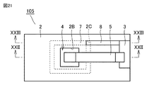
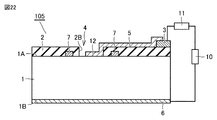
- FIG. 5 is a schematic cross-sectional view of the line segment XXII-XXII in FIG. 21. It is sectional drawing of the line segment XXIII-XXIII in FIG. 21. It is sectional drawing which shows the electromagnetic wave detector which concerns on Embodiment 7.
- FIG. 5 is a schematic cross-sectional view of the line segment XXVI-XXVI in FIG. 24. It is a plane schematic diagram which shows the modification of the electromagnetic wave detector which concerns on Embodiment 7.
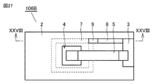
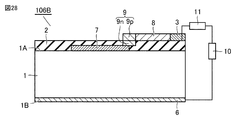
- FIG. 6 is a schematic cross-sectional view of the line segment XXVIII-XXVIII in FIG. 27. It is a plane schematic diagram which shows the electromagnetic wave detector which concerns on Embodiment 8.
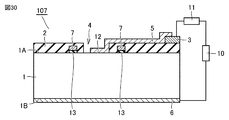
- FIG. 5 is a schematic cross-sectional view taken along the line segment XXX-XXX in FIG. 29. It is a plane schematic diagram which shows the electromagnetic wave detector which concerns on Embodiment 9.
- FIG. 3 is a schematic cross-sectional view of the line segment XXXII-XXXII in FIG. 31. It is a plane schematic diagram which shows the electromagnetic wave detector which concerns on Embodiment 10.
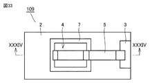
- FIG. 3 is a schematic cross-sectional view of the line segment XXXIV-XXXIV in FIG. 33. It is a plane schematic diagram of the electromagnetic wave detector array which concerns on Embodiment 11.
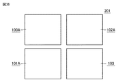
- FIG. It is a plan schematic diagram which shows the modification of the electromagnetic wave detector array which concerns on Embodiment 11.
- the figure is schematic and conceptually describes the function or structure. Further, the present invention is not limited to the embodiments described below. Unless otherwise specified, the basic configuration of the electromagnetic wave detector is common to all embodiments. Further, those having the same reference numerals are the same or equivalent as described above. This is common throughout the specification.
- the electromagnetic wave detector will be described using a configuration for detecting visible light or infrared light, but the present invention is not limited thereto.
- the embodiment described below is a detector that detects radio waves such as X-rays, ultraviolet light, near-infrared light, terahertz (THH) waves, or microwaves in addition to visible light or infrared light. It is also effective as.
- these light and radio waves are collectively referred to as electromagnetic waves.
- p-type graphene or n-type graphene may be used as graphene.
- graphene having more holes than graphene in the intrinsic state is called p-type graphene
- graphene having more electrons is called n-type graphene.
- the n-type or p-type term may be used for the material of the member in contact with graphene, which is an example of the two-dimensional material layer.
- the n-type material is a material having an electron donating property
- the p-type material is a material having an electron attracting property.
- the charge is biased in the whole molecule, and the one in which electrons are dominant is called n-type, and the one in which holes are dominant is called p-type.
- these materials either one of organic substances and inorganic substances or a mixture thereof can be used.
- the material of the two-dimensional material layer is not limited to graphene.
- the materials of the two-dimensional material layer include transition metal dichalcogenide (TMD), black phosphorus (Black Phosphorus), silicene (two-dimensional honeycomb structure with silicon atoms), and germanene (two-dimensional honeycomb structure with germanium atoms). ) And other materials can be applied.
- transition metal dichalcogenide include transition metal dicalcogenides such as molybdenum disulfide (MoS 2 ), tungsten sulfide (WS 2 ), and tungsten diselinated (WSe 2).
- These materials have a structure similar to graphene, and are materials capable of arranging atoms in a two-dimensional plane in a single layer. Therefore, even when these materials are applied to the two-dimensional material layer, the same action and effect as when graphene is applied to the two-dimensional material layer can be obtained.
- the electromagnetic wave detector 100A includes a semiconductor substrate 1, a first insulating film 2, a first electrode 3, a two-dimensional material layer 5, a second electrode 6, and The control electrode 7 is mainly provided.
- the semiconductor substrate 1 has a first surface 1A and a second surface 1B.
- the second surface 1B is located on the opposite side of the first surface 1A.
- the first surface 1A and the second surface 1B are, for example, flat surfaces.
- the semiconductor substrate 1 has sensitivity to a predetermined detection wavelength from the above-mentioned electromagnetic waves.
- the semiconductor substrate 1 has an n-type or p-type conductive type, and is provided so that an optical carrier is generated in the semiconductor substrate 1 when an electromagnetic wave having a predetermined detection wavelength is incident on the semiconductor substrate 1. There is.
- the semiconductor material constituting the semiconductor substrate 1 can be arbitrarily selected according to the detection wavelength that should have sensitivity.
- the semiconductor material constituting the semiconductor substrate 1 is, for example, a compound semiconductor such as silicon (Si), germanium (Ge), III-V group semiconductor or II-V group semiconductor, HgCdTe, InSb, lead selenium (PbSe), lead sulfur ( Selected from the group consisting of PbS), cadmium sulfur (CdS), gallium nitride (GaN), silicon carbide (SiC), gallium phosphide (GaP), indium gallium arsenide (InGaAs), and indium arsenide (InAs). Includes at least one.
- a compound semiconductor such as silicon (Si), germanium (Ge), III-V group semiconductor or II-V group semiconductor, HgCdTe, InSb, lead selenium (PbSe), lead sulfur ( Selected from the group consisting of PbS), cadmium sulfur (CdS), gallium nitride (GaN), silicon carbide (SiC), gallium pho
- the semiconductor substrate 1 may be, for example, a substrate containing quantum wells or quantum dots made of two or more semiconductor materials selected from the above group, a substrate containing a Type II superlattice, or a substrate containing them. It may be a combined substrate.
- the first insulating film 2 is arranged on the first surface 1A of the semiconductor substrate 1.
- the first electrode 3 is arranged on the first insulating film 2.
- the first insulating film 2 is formed so as to expose a part of the first surface 1A of the semiconductor substrate 1.
- a part of the first surface 1A of the semiconductor substrate 1 is configured as an exposed portion 4 exposed from the first insulating film 2.
- the first insulating film 2 is formed at a distance from a part of the first insulating film 2 that overlaps with the first electrode 3 in a plan view, and has an end surface 2A extending in a direction intersecting the first surface 1A. doing.
- the material constituting the first insulating film 2 and the thickness of the first insulating film 2 are selected so as to prevent a tunnel current from being generated between the semiconductor substrate 1 and the first electrode 3.
- the materials constituting the first insulating film 2 include, for example, silicon oxide (SiO 2 ), silicon nitride (Si 3 N 4 ), hafnium oxide (HfO 2 ), aluminum oxide (Al 2 O 3 ), nickel oxide (NiO), and the like. And at least one selected from the group consisting of boron nitride (BN).
- the first electrode 3 is arranged on the first insulating film 2 at a position away from the end face 2A.
- the first electrode 3 is electrically connected to the two-dimensional material layer 5.
- the second electrode 6 is in contact with the semiconductor substrate 1.
- the second electrode 6 is in contact with, for example, the second surface 1B of the semiconductor substrate 1.
- the second electrode 6 is ohmic-bonded to the semiconductor substrate 1.
- the power supply circuit includes a power supply 11 that applies a voltage between the first electrode 3 and the second electrode 6, and an ammeter 10 that measures the current flowing between the first electrode 3 and the second electrode 6.
- the material constituting the first electrode 3 and the second electrode 6 may be any conductor, but is preferably a material for ohmic bonding with the semiconductor substrate 1, for example, gold (Au), silver (Ag), copper ( Includes at least one selected from the group consisting of Cu), aluminum (Al), nickel (Ni), chromium (Cr), and palladium (Pd).
- An adhesion layer (not shown) that enhances the adhesion between the first electrode 3 and the first insulating film 2 may be formed between the first electrode 3 and the first insulating film 2.
- An adhesion layer (not shown) that enhances the adhesion between the second electrode 6 and the semiconductor substrate 1 may be formed between the second electrode 6 and the semiconductor substrate 1.
- the material constituting the adhesion layer includes, for example, a metal material such as chromium (Cr) or titanium (Ti).
- the two-dimensional material layer 5 has a joint portion 12 that is Schottky-bonded to at least a part of the exposed portion 4.
- the Schottky bonding between the two-dimensional material layer 5 and the semiconductor substrate 1 is referred to as a first Schottky bonding.
- the two-dimensional material layer 5 is in contact with, for example, a part of the exposed portion 4.
- the two-dimensional material layer 5 extends from the joint portion 12 to the first electrode 3 via the first insulating film 2.
- the two-dimensional material layer 5 has, for example, a longitudinal direction and a direction intersecting the longitudinal direction and a lateral direction. One end of the two-dimensional material layer 5 in the longitudinal direction forms a joint portion 12. The entire part of the two-dimensional material layer 5 in the lateral direction at one end in the longitudinal direction forms the joint portion 12. The other end of the two-dimensional material layer 5 in the longitudinal direction is electrically connected to the first electrode 3.
- the two-dimensional material layer 5 is, for example, single-layer graphene or multi-layer graphene.
- the two-dimensional material layer 5 may include, for example, graphene nanoribbons.
- the two-dimensional material layer 5 may include a random layer laminated graphene composed of a plurality of single-layer graphenes.
- the material constituting the two-dimensional material layer 5 may contain at least one selected from the group consisting of graphene, transition metal dichalcogenides, black phosphorus, silicene, and germanene. Further, the two-dimensional material layer 5 may have a hetero-laminated structure in which two or more materials selected from the above group are combined.
- a protective film (not shown) may be formed on the two-dimensional material layer 5.
- the material constituting such a protective film contains, for example, at least one selected from the group consisting of SiO 2 , Si 3 N 4 , HfO 2 , Al 2 O 3, NiO, and BN.
- the control electrode 7 is arranged in a part around the joint portion 12 in a plan view, and is Schottky-bonded to the semiconductor substrate 1.
- the Schottky junction between the control electrode 7 and the semiconductor substrate 1 is referred to as a second Schottky junction.
- the control electrode 7 is in contact with the first surface 1A of the semiconductor substrate 1.
- the control electrode 7 is arranged at a distance from the joint portion 12, for example.
- the control electrode 7 is covered with, for example, the first insulating film 2.
- the control electrode 7 is not in direct contact with the two-dimensional material layer 5.
- the control electrode 7 is not connected to the power supply.
- the two-dimensional material layer 5 and the control electrode 7 are connected so that the depletion layer of the second Schottky junction is connected to the depletion layer formed in the first Schottky junction when a reverse bias is applied to the first Schottky junction. Have been placed.
- the two-dimensional material layer 5 and the control electrode 7 are formed by connecting the depletion layer of the second Schottky junction to the depletion layer formed in the first Schottky junction when a reverse bias is applied to the first Schottky junction.
- the entire depletion layer formed is arranged so as to cover the entire interface of the first Schottky junction.
- the control electrode 7 is arranged on the side opposite to the first electrode 3 with respect to the joint portion 12, for example, in the longitudinal direction of the two-dimensional material layer 5.
- the control electrode 7 has, for example, a longitudinal direction and a lateral direction intersecting the longitudinal direction.
- the longitudinal direction of the control electrode 7 is, for example, along the lateral direction of the two-dimensional material layer 5.
- the lateral direction of the control electrode 7 is, for example, along the longitudinal direction of the two-dimensional material layer 5.
- the width of the control electrode 7 in the longitudinal direction is equal to or greater than the width of the two-dimensional material layer 5 in the lateral direction.
- the width of the control electrode 7 in the longitudinal direction is wider than, for example, the width of the two-dimensional material layer 5 in the lateral direction.
- the width of the joint portion 12 in the longitudinal direction of the two-dimensional material layer 5 is wider than the width of the control electrode 7 in the lateral direction, for example.
- the material constituting the control electrode 7 includes a metal material that is Schottky-bonded to the semiconductor substrate 1.
- the material constituting the control electrode 7 is a metal having a larger work function than the semiconductor material constituting the semiconductor substrate 1.
- the material constituting the control electrode 7 has a second Schottky junction barrier height (difference between the work function of the material constituting the control electrode 7 and the electron affinity of the material constituting the semiconductor substrate 1). It is a metal selected to be higher than the barrier height of the 1-Schottky junction (the difference between the work function of the material constituting the two-dimensional material layer 5 and the electron affinity of the material constituting the semiconductor substrate 1).
- the material constituting the control electrode 7 includes, for example, at least one of Au and Ni.
- the material constituting the control electrode 7 is a metal having a work function smaller than that of the semiconductor material constituting the semiconductor substrate 1.
- the material constituting the control electrode 7 contains, for example, at least one of indium (In) and tin (Sn).
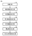
- FIG. 3 is a flowchart for explaining a method of manufacturing the electromagnetic wave detector according to the first embodiment. A method of manufacturing the electromagnetic wave detector shown in FIGS. 1 and 2 will be described with reference to FIG.
- the preparation step (S1) shown in FIG. 3 is carried out.
- a flat semiconductor substrate 1 is prepared.
- the semiconductor substrate 1 has a first surface 1A and a second surface 1B.
- the semiconductor material constituting the semiconductor substrate 1 is a semiconductor material having sensitivity to a predetermined detection wavelength.
- control electrode forming step (S2) is carried out.
- the control electrode 7 is formed on the first surface 1A of the semiconductor substrate 1.
- the method for forming the control electrode 7 is not particularly limited, and includes, for example, a film forming process by a vapor deposition method or a sputtering method, a photoplate making process, and an etching process.
- the second electrode forming step (S3) is carried out.
- the second electrode 6 is formed on the second surface 1B of the semiconductor substrate 1.
- the method for forming the second electrode 6 is not particularly limited, and includes, for example, a film forming process by a vapor deposition method or a sputtering method, a photoengraving process, and an etching process.
- the above-mentioned adhesion layer is previously formed in the region connected to the second electrode 6 in the semiconductor substrate 1. You may leave it.
- the insulating film forming step (S4) is carried out.
- the first insulating film 2 is formed on the first surface 1A of the semiconductor substrate 1.
- the method for forming the first insulating film 2 is not particularly limited, and is, for example, a plasma CVD (Chemical Vapor Deposition) method or an atomic layer volumetric method (ALD).
- a barrier film may be formed between the semiconductor substrate 1 and the first insulating film 2 immediately before the main insulating film forming step (S4).
- the material constituting the barrier film may be a material having a higher resistance to the etchant used in the exposed portion forming step (S6) than the material constituting the first insulating film 2 (a material having a slow etching rate).
- silicon nitride (SiN), aluminum oxide (Al 2 O 3 ), or graphene for example, silicon nitride (SiN), aluminum oxide (Al 2 O 3 ), or graphene.
- the first electrode forming step (S5) is carried out.
- the first electrode 3 is formed on the first insulating film 2.
- the method for forming the first electrode 3 is not particularly limited, and includes, for example, a film forming process by a vapor deposition method or a sputtering method, a photoengraving process, and an etching process.
- the above-mentioned adhesion is formed in the region connected to the first electrode 3 in the first insulating film 2.
- the layer may be formed in advance.
- the exposed portion forming step (S6) is carried out.
- a part of the first insulating film 2 is removed to form an exposed portion 4 exposed from the first insulating film 2 on the semiconductor substrate 1.
- a resist mask is formed on the first insulating film 2 by photoengraving or EB drawing.
- the resist mask is formed so as to cover the region where the first insulating film 2 should be formed and to expose the region where the exposed portion 4 should be formed.
- the first insulating film 2 is etched using the resist mask as an etching mask.
- the etching method can be arbitrarily selected from either wet etching using hydrofluoric acid or dry etching using a reactive ion etching method or the like. After etching, the resist mask is removed. In this way, the exposed portion 4 is formed.
- the above step (S6) may be performed before the step (S5).
- the two-dimensional material layer forming step (S7) is carried out.
- the two-dimensional material layer 5 is formed on at least a part of each of the first insulating film 2 and the exposed portion 4.
- the method for forming the two-dimensional material layer 5 is not particularly limited, and includes a film forming process by an epitaxial growth method, a photoplate making process, and an etching process.
- the electromagnetic wave detector 100A shown in FIGS. 1 and 2 is manufactured.
- the exposed portion forming step (S6) may be performed before the first electrode forming step (S5). That is, in the method for manufacturing the electromagnetic wave detector 100A, the above-mentioned step (S1), the above-mentioned step (S2), the above-mentioned step (S3), the above-mentioned step (S4), the above-mentioned step (S6), the above-mentioned step (S5), and the above-mentioned step. (S7) may be carried out in this order of description.
- FIG. 4 is a schematic cross-sectional view showing an operation example of the electromagnetic wave detector 100A.
- a power supply circuit (not shown) is electrically connected between the first electrode 3 and the second electrode 6.
- the power supply circuit includes a power supply 11 that applies a voltage V between the first electrode 3 and the second electrode 6, and an ammeter 10 that measures a current I flowing through the power supply circuit.
- the positive or negative voltage is selected according to the conductive type (doping type) of the semiconductor substrate 1 so that the reverse bias is applied to the first Schottky junction.
- the voltage applied to both of the power supply 11 so that the potential of the first electrode 3 is higher than the potential of the second electrode 6 is set as a positive voltage.
- the electromagnetic wave detector 100A is in a state in which the semiconductor substrate 1 can detect an electromagnetic wave having a wavelength having sensitivity.
- the electromagnetic wave detector 100A In a state where the electromagnetic wave detector 100A can detect an electromagnetic wave, a reverse bias is applied to the first Schottky junction. Therefore, the depletion layer at the interface of the first Schottky junction extends around it and is connected to the depletion layer of the second Schottky junction. As a result, in the electromagnetic wave detector 100A in which the first Schottky junction and the second Schottky junction are formed, the dark current is reduced as compared with the electromagnetic wave detector in which only the first Schottky junction is formed.
- FIG. 5 is a graph showing an operation example of the electromagnetic wave detector 100A.
- the horizontal axis of FIG. 5 shows the voltage (unit: V) applied by the power supply 11 to the first Schottky junction, and the vertical axis of FIG. 5 shows the current value (unit: A) measured by the ammeter 10.
- the solid line in FIG. 5 indicates a state in which the electromagnetic wave detector 100A in a state in which the electromagnetic wave can be detected is not irradiated with the electromagnetic wave, and the dotted line in FIG. 5 indicates a state in which the electromagnetic wave detector 100A in a state in which the electromagnetic wave can be detected. Shows the state of being irradiated with electromagnetic waves.
- the dark current is kept low when the electromagnetic wave detector 100A is not irradiated with electromagnetic waves.
- the electromagnetic wave detector 100A when the electromagnetic wave detector 100A is irradiated with electromagnetic waves, optical carriers are generated in the depletion layer of the semiconductor substrate 1.
- the reverse current increases and the current I changes.
- the current component that causes a change in the current I due to the irradiation of electromagnetic waves in this way is called a photocurrent.
- the conductive type of the semiconductor substrate 1 is n-type, the holes flow into the two-dimensional material layer 5, so that the reverse current increases and the current I changes.
- a depletion layer is also formed at the interface between the semiconductor substrate 1 and the first insulating film 2.
- optical carriers for example, holes when the conductive type of the semiconductor substrate 1 is n-type
- the semiconductor substrate 1 and the first insulating film 2 are formed. Accumulates at the interface of.
- the optical carriers accumulated at the interface modulate the carrier density of the two-dimensional material layer 5 that acts as a channel through the first insulating film 2, similar to the gate voltage of the transistor.
- the conductivity of the two-dimensional material layer 5 changes, and the current I flowing through the two-dimensional material layer 5 changes.
- This effect is called the optical gate effect. Since the current due to the photocarrier generated by the photoelectric conversion of the semiconductor substrate 1 is amplified by the optical gate effect, the quantum efficiency calculated from the photocurrent becomes an extremely large value. Therefore, the detection sensitivity of the electromagnetic wave detector 100A is high.
- a second Schottky junction between the control electrode 7 and the semiconductor substrate 1 is formed around the first Schottky junction between the two-dimensional material layer 5 and the semiconductor substrate 1. Therefore, in the electromagnetic wave detector 100A, the depletion layer at the interface of the first Schottky junction may be connected to the depletion layer of the second Schottky junction by applying a predetermined reverse bias to the first Schottky junction. can.
- the dark current in the first Schottky junction is reduced as compared with the electromagnetic wave detector in which only the first Schottky junction is formed. ing.
- the two-dimensional material layer forming step (S7) is performed after the insulating film forming step (S4) and the exposed portion forming step (S6), whereas the control electrode forming step (S2) Is performed before the insulating film forming step (S4) and the exposed portion forming step (S6). Therefore, the region on the first surface 1A on which the control electrode 7 should be formed in the control electrode forming step (S2) is the first surface on which the two-dimensional material layer 5 should be formed in the two-dimensional material layer forming step (S7). The foreign matter is less likely to remain than in the region above 1A.
- the barrier height of the second Schottky junction (difference between the work function of the material constituting the control electrode 7 and the electron affinity of the material constituting the semiconductor substrate 1) for each electromagnetic wave detector 100A.
- the variation is larger than the variation in the barrier height of the first Schottky junction (difference between the work function of the material constituting the two-dimensional material layer 5 and the electron affinity of the material constituting the semiconductor substrate 1) for each electromagnetic detector 100A. It has been reduced.
- the electromagnetic wave detector 100A the variation in the dark current for each electromagnetic wave detector 100A is reduced as compared with the electromagnetic wave detector in which only the first Schottky junction is formed.
- the material constituting the control electrode 7 is a metal material
- the bonding interface of the second Schottky junction between the control electrode 7 and the semiconductor substrate 1 is the first Schottky between the two-dimensional material layer 5 and the semiconductor substrate 1.
- the residual foreign matter can be more easily suppressed than the joining interface of the joining.
- the Fermi level of the metal material constituting the control electrode 7 is less likely to be modulated than the Fermi level of the material constituting the two-dimensional material layer 5. Therefore, in the electromagnetic wave detector 100A, the variation in the barrier height of the second Schottky junction for each electromagnetic wave detector 100A is smaller than the variation in the barrier height for the first Schottky junction for each electromagnetic wave detector 100A. .. As a result, in the electromagnetic wave detector 100A, the variation in the dark current for each electromagnetic wave detector 100A is reduced as compared with the electromagnetic wave detector in which only the first Schottky junction is formed.
- the barrier height of the second Schottky junction can be made higher than the barrier height of the first Schottky junction.
- the voltage range (low dark current region in FIG. 4) in which the dark current is reduced is wider than that of the electromagnetic wave detector in which only the first Schottky junction is formed. That is, in the electromagnetic wave detector 100A, a larger negative voltage can be applied between the first electrode 3 and the second electrode 6 as compared with the electromagnetic wave detector in which only the first Schottky junction is formed.
- the depletion layer extends to a deeper region with respect to the first surface 1A as compared with the electromagnetic wave detector in which only the first Schottky junction is formed, so that it is generated by irradiation with electromagnetic waves. More photocarriers can be taken out.
- the semiconductor substrate 1 is an n-type Si substrate
- the two-dimensional material layer 5 is a single-layer graphene
- the material constituting the control electrode 7 is Ni
- the work of the materials constituting the two-dimensional material layer 5 The difference between the function and the electron affinity of the material constituting the semiconductor substrate 1 is 0.95 eV, and the difference between the work function of the material constituting the control electrode 7 and the electron affinity of the material constituting the semiconductor substrate 1 is 1.17 eV. ..
- the number of electrons IMS from the metal to the semiconductor in the Schottky junction is expressed as follows using the proportionality constant K, the Boltzmann constant k, the temperature T, and the barrier height ⁇ B.
- the barrier height of the second Schottky junction is 0.22 eV higher than the barrier height of the first Schottky junction
- the number of electrons IMS estimated from the former barrier height is the electron estimated from the latter barrier height. It is about 4 orders of magnitude smaller than a few IMS. Therefore, in the electromagnetic wave detector 100A in which the barrier height of the second Schottky junction is higher than the barrier height of the first Schottky junction, the electromagnetic wave detector in which only the first Schottky junction is formed and the barrier of the second Schottky junction are formed.
- the dark current can be reduced as compared with the electromagnetic wave detector 100A whose height is comparable to the barrier height of the first Schottky junction.
- the electromagnetic wave detector 100A a semiconductor substrate in a region overlapping the two-dimensional material layer 5 in a plan view, that is, a region directly below the two-dimensional material layer 5, as compared with the electromagnetic wave detector in which only the first Schottky junction is formed.
- the amount of optical carriers accumulated at the interface between 1 and the first insulating film 2 increases. Therefore, in the electromagnetic wave detector 100A, the optical gate effect is amplified and the photocurrent is increased as compared with the electromagnetic wave detector in which only the first Schottky junction is formed.
- the change amount of the photocurrent is increased because the photoelectric flow rate is increased while the variation in the dark current is reduced as compared with the electromagnetic wave detector in which only the first Schottky junction is formed. It becomes large and the detection sensitivity is high.
- ⁇ Modification example> 6 and 7 are diagrams showing an electromagnetic wave detector 100B which is a modification of the electromagnetic wave detector 100A.
- the second electrode 6 is in contact with the first surface 1A.
- the second electrode 6 is arranged on the side opposite to the two-dimensional material layer 5 and the first electrode 3 with respect to the control electrode 7, for example.
- the control electrode 7 is arranged between the joint portion 12 of the two-dimensional material layer 5 and the second electrode 6.
- the width of the control electrode 7 in the longitudinal direction is, for example, wider than the width of the second electrode 6 in the longitudinal direction.
- the arrangement of the second electrode 6 is not particularly limited as long as it is in contact with the semiconductor substrate 1.
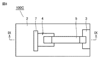
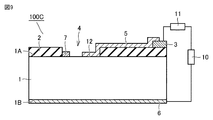
- FIGS. 8 and 9 are diagrams showing an electromagnetic wave detector 100C which is a modification of the electromagnetic wave detector 100A.
- the control electrode 7 is arranged on the exposed portion 4 of the semiconductor substrate 1.
- the control electrode 7 is exposed from the first insulating film 2.
- a part of the control electrode 7 may be covered with the first insulating film 2, and the other part of the control electrode 7 may be exposed from the first insulating film 2.
- the first insulating film 2 is formed by at least a portion of the two-dimensional material layer 5 located between the first electrode 3 and the semiconductor substrate 1 and between the joint portion 12 and the first electrode 3 and the semiconductor substrate 1. It suffices if it is formed so that a tunnel current is not generated between them. That is, in the electromagnetic wave detectors 100A, 100B, and 100C, most of the first surface 1A of the semiconductor substrate 1 may be configured as the exposed portion 4.
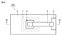
- Embodiment 2. 10 and 11 are diagrams showing the electromagnetic wave detector 101 according to the second embodiment. As shown in FIGS. 10 and 11, the electromagnetic wave detector 101 has basically the same configuration as the electromagnetic wave detector 100A, but the control electrode 7 sandwiches the joint portion 12 in a plan view. It differs from the electromagnetic wave detector 100A in that it is arranged in the surroundings.
- the electromagnetic wave detector 101B includes one control electrode 7 formed in an annular shape in a plan view.
- the control electrode 7 is arranged around the joint portion 12 so as to surround the entire circumference of the joint portion 12.
- the control electrodes 7 are arranged around the joint portion 12 so as to sandwich the joint portion 12 in each of the longitudinal direction and the lateral direction of the two-dimensional material layer 5.
- a pair of portions arranged so as to sandwich the joint portion 12 in the longitudinal direction of the two-dimensional material layer 5 have a line-symmetrical relationship with each other, for example, with respect to the joint portion 12.
- a pair of portions arranged so as to sandwich the joint portion 12 in the lateral direction of the two-dimensional material layer 5 have a line-symmetrical relationship with each other, for example, with respect to the joint portion 12.
- the control electrode 7 is covered with, for example, the first insulating film 2. In a plan view, the control electrode 7 is arranged around the joint portion 12 so as to surround the entire circumference of the exposed portion 4, for example.
- a part of the control electrode 7 is arranged so as to overlap the portion of the two-dimensional material layer 5 located between the joint portion 12 and the first electrode 3. In other words, a part of the control electrode 7 is arranged directly below the portion of the two-dimensional material layer 5 located between the joint portion 12 and the first electrode 3.
- the electromagnetic wave detector 101 Since the electromagnetic wave detector 101 has basically the same configuration as the electromagnetic wave detector 100A, the same effect as that of the electromagnetic wave detector 100A can be obtained.
- the depletion layer of the second Schottky junction between the control electrode 7 and the semiconductor substrate 1 is arranged so as to sandwich the depletion layer of the first Schottky junction between the semiconductor substrate 1 and the two-dimensional material layer 5. Therefore, the depletion layer formed when the reverse bias is applied to the first Schottky junction can more reliably cover the entire interface of the first Schottky junction. Therefore, in the electromagnetic wave detector 101, the variation in the dark current for each electromagnetic wave detector 100A is reduced more stably than in the electromagnetic wave detector 100A.
- the electromagnetic wave detector 101 may include a plurality of control electrodes 7 arranged so as to be spaced apart from each other in the circumferential direction surrounding the joint portion 12.
- the plurality of control electrodes 7 are joined to, for example, a pair of control electrodes 7 arranged so as to sandwich the joint portion 12 in the longitudinal direction of the two-dimensional material layer 5 in the lateral direction of the two-dimensional material layer 5. It includes a pair of control electrodes 7 arranged so as to sandwich the portion 12.
- the electromagnetic wave detector 101 may include a plurality of control electrodes 7 formed in an annular shape in a plan view.
- the plurality of control electrodes 7 include a first control electrode arranged on the innermost side, and a second control electrode arranged so as to surround the joint portion 12 and the first control electrode.
- the electromagnetic wave detector 101 may have the same configuration as the electromagnetic wave detectors 100B and 100C, except that the control electrode 7 is arranged around the joint portion 12 so as to sandwich the joint portion 12 in a plan view. ..
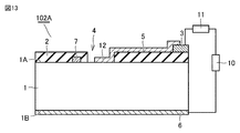
- Embodiment 3. 12 and 13 are views showing the electromagnetic wave detector 102A according to the third embodiment.
- the electromagnetic wave detector 102A has basically the same configuration as the electromagnetic wave detector 101 according to the second embodiment, but the control electrode 7 is a two-dimensional material in a plan view. It differs from the electromagnetic wave detector 101 in that it is arranged in a region that does not overlap with the layer 5. In other words, the control electrode 7 is not arranged directly below the two-dimensional material layer 5.
- the control electrode 7 has a C-shape so as to surround a part around the joint portion 12, for example.
- the control electrode 7 has, for example, an end portion 7A and an end portion 7B arranged so as to sandwich the two-dimensional material layer 5 in the lateral direction of the two-dimensional material layer 5.
- the distance between the end portion 7A and the end portion 7B is narrower than, for example, the width of the exposed portion 4.
- control electrode 7 When the control electrode 7 is arranged so as to overlap the two-dimensional material layer 5 in a plan view as in the electromagnetic wave detector 101 shown in FIG. 11, optical carriers are not accumulated at the interface between the control electrode 7 and the semiconductor substrate 1. .. Therefore, of the two-dimensional material layer 5 arranged on the first insulating film 2, the optical gate effect is not exhibited in the portion arranged on the control electrode 7.
- the electromagnetic wave detector 102A since the control electrode 7 is arranged in a region that does not overlap with the two-dimensional material layer 5 in a plan view, the optical gate effect is two-dimensionally arranged on the first insulating film 2. It is expressed throughout the material layer 5. Therefore, the electromagnetic wave detector 102A has a higher photocurrent amplification factor due to the optical gate effect than the electromagnetic wave detector 101.
- the first insulating film 2 is arranged between the two-dimensional material layer 5 and the control electrode 7 arranged immediately below the two-dimensional material layer 5.
- the portion of the first insulating film 2 arranged on the control electrode 7 protrudes from the portion arranged on the semiconductor substrate 1 by the thickness of the control electrode 7. That is, a convex portion due to the control electrode 7 is formed on the upper surface of the first insulating film 2.
- the electromagnetic wave detector 102A since the control electrode 7 is not arranged directly under the two-dimensional material layer 5, the first insulating film 2 arranged between the two-dimensional material layer 5 and the semiconductor substrate 1 is It is flat. Therefore, in the electromagnetic wave detector 102A, the problem caused by the convex portion of the first insulating film 2 as described above does not occur.
- the electromagnetic wave detector 102A can exert the same effect as the electromagnetic wave detector 101 in addition to the above effects.
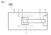
- FIG. 14 is a diagram showing an electromagnetic wave detector 102B which is a modification of the electromagnetic wave detector 102A.
- the electromagnetic wave detector 102B includes a plurality of control electrodes 7.
- the plurality of control electrodes 7 are arranged around the joint portion 12 so as to sandwich the joint portion 12 in at least one direction.
- the plurality of control electrodes 7 are arranged so as to sandwich the joint portion 12 in the lateral direction of the two-dimensional material layer 5, for example.
- the plurality of control electrodes 7 are covered with, for example, the first insulating film 2.
- the plurality of control electrodes 7 are arranged around the joint portion 12 so as to sandwich the exposed portion 4, for example.
- Each control electrode 7 has, for example, a longitudinal direction and a lateral direction.
- the longitudinal direction of each control electrode 7 is, for example, along the longitudinal direction of the two-dimensional material layer 5.
- the width of each control electrode 7 in the longitudinal direction is, for example, wider than the width of the joint portion 12 in that direction.
- One end of each control electrode 7 in the longitudinal direction is arranged on the first electrode 3 side of the joint portion 12, for example.
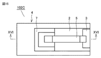
- FIGS. 15 and 16 are diagrams showing an electromagnetic wave detector 102C which is a modification of the electromagnetic wave detector 102A.
- the electromagnetic wave detector 102C most of the first surface 1A of the semiconductor substrate 1 is configured as the exposed portion 4.
- the first insulating film 2 is formed between the first electrode 3 and the semiconductor substrate 1, and between the portion of the two-dimensional material layer 5 located between the joint portion 12 and the first electrode 3 and the semiconductor substrate 1. , It is formed so that no tunnel current is generated.
- the control electrode 7 is arranged on the exposed portion 4. In other words, the control electrode 7 is exposed from the first insulating film 2.
- the electromagnetic wave detector 102A may have the same configuration as the electromagnetic wave detectors 100B and 100C, except that the control electrode 7 is arranged in a region that does not overlap with the two-dimensional material layer 5 in a plan view.
- Embodiment 4. 17 and 18 are diagrams showing the electromagnetic wave detector 103 according to the fourth embodiment.
- the electromagnetic wave detector 103 shown in FIGS. 17 and 18 has basically the same configuration as the electromagnetic wave detector 101 according to the second embodiment, but the electromagnetic wave detection is performed in that the control electrode 7 is grounded. It is different from the vessel 101.
- the control electrode 7 is electrically connected to the ground node 13.
- a part of the control electrode 7 is exposed from the first insulating film 2, and the part of the control electrode 7 is electrically connected to a ground wire electrically connected to the ground node 13.
- the potential of the control electrode 7 is fixed. Therefore, even when a relatively large voltage is applied between the first electrode 3 and the second electrode 6, the potential of the control electrode 7 does not rise, and the second Schottky junction between the control electrode 7 and the semiconductor substrate 1 is performed. Barrier height does not decrease.
- the dark current can be reduced even when a relatively large voltage is applied between the first electrode 3 and the second electrode 6.
- the control electrodes 7 of each electromagnetic wave detector 103 may be individually electrically connected to the ground node 13. Further, in the electromagnetic wave detector array configured in which a plurality of electromagnetic wave detectors 103 are connected to each other, the control electrodes 7 of each electromagnetic wave detector 103 are electrically connected to each other to form a part of one ground wire. One point of the ground wire may be electrically connected to the ground node 13. In the latter electromagnetic wave detector array, the degree of integration of the electromagnetic wave detector 103 can be increased as compared with the former electromagnetic wave detector array.
- the electromagnetic wave detector 103 can exert the same effect as the electromagnetic wave detector 101 in addition to the above effects.
- the electromagnetic wave detector 103 may have the same configuration as the electromagnetic wave detectors 100A, 100B, 100C, 102A, 102B, 102C except that the control electrode 7 is grounded.
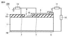
- Embodiment 5 19 and 20 are views showing the electromagnetic wave detector 104 according to the fifth embodiment. As shown in FIGS. 19 and 20, the electromagnetic wave detector 104 has basically the same configuration as the electromagnetic wave detector 101 according to the second embodiment, but the control electrode 7 is connected to the power supply 14. In that respect, it differs from the electromagnetic wave detector 101.
- the electromagnetic wave detector 104 applies a voltage (second voltage) to the power supply 11 (first power supply) that applies a voltage (first voltage) between the first electrode 3 and the second electrode 6 and the control electrode 7.
- a power source 14 (second power source) is provided.
- the barrier height of the second Schottky junction between the control electrode 7 and the semiconductor substrate 1 can be arbitrarily set.
- the barrier height is set so that, for example, a low dark current region is formed widely and stably with respect to the voltage applied to the first electrode 3.
- the electromagnetic wave detector 104 by applying a voltage to the control electrode 7, the electromagnetic wave detector 104 is formed at the interface between the first insulating film 2 directly below the two-dimensional material layer 5 and the semiconductor substrate 1 as compared with the electromagnetic wave detector 101.
- the internal electric field of the depletion layer can be increased.
- the larger the internal electric field of the depletion layer the more photocarriers are accumulated at the interface. Therefore, the electromagnetic wave detector 104 has a higher photocurrent amplification factor due to the optical gate effect than the electromagnetic wave detector 101.
- the electromagnetic wave detector 104 can exhibit the same effect as the electromagnetic wave detector 100A in addition to the above effects.
- the electromagnetic wave detector 104 may have the same configuration as the electromagnetic wave detectors 100A, 100B, 100C, 102A, 102B, 102C, except that the control electrode 7 is connected to the power supply 14.
- Embodiment 6. 21 to 23 are views showing the electromagnetic wave detector 105 according to the sixth embodiment. As shown in FIGS. 21 to 23, the electromagnetic wave detector 105 has basically the same configuration as the electromagnetic wave detector 101 according to the second embodiment, but the control electrode 7 is electrically connected to the first electrode 3. It differs from the electromagnetic wave detector 101 in that it is connected to the electromagnetic wave detector 101.
- the control electrode 7 is electrically connected to the first electrode 3 via, for example, a lead-out electrode 8.
- the extraction electrode 8 is arranged on the first insulating film 2 and the control electrode 7.
- the first insulating film 2 is formed with an opening 2B for exposing the exposed portion 4 of the semiconductor substrate 1 and an opening 2C for exposing a part of the control electrode 7. In a plan view, the openings 2C are arranged at intervals from, for example, the openings 2B.
- the above-mentioned step (S1), the above-mentioned step (S2), the above-mentioned step (S3), the above-mentioned step (S4), the above-mentioned step (S6), the above-mentioned step (S5), and the above-mentioned step. (S7) is carried out in this order of description.
- the opening 2B and the opening 2C are formed at the same time, for example, in the exposed portion forming step (S6).
- the first electrode 3 and the extraction electrode 8 are simultaneously formed in the first electrode forming step (S5) performed after the exposed portion forming step (S6).
- the potential of the control electrode 7 is kept constant. Therefore, even when a relatively large voltage is applied between the first electrode 3 and the second electrode 6, the potential of the control electrode 7 does not rise, and the second Schottky junction between the control electrode 7 and the semiconductor substrate 1 is performed. Barrier height does not decrease. Therefore, in the electromagnetic wave detector 105, the dark current can be reduced even when a relatively large voltage is applied between the first electrode 3 and the second electrode 6.
- the electromagnetic wave detector 105 can exert the same effect as the electromagnetic wave detector 101 in addition to the above effects.
- the electromagnetic wave detector 105 has the same configuration as the electromagnetic wave detectors 100A, 100B, 100C, 102A, 102B, 102C except that the control electrode 7 is electrically connected to the first electrode 3. You may.
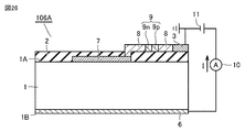
- Embodiment 7. 24 to 26 are views showing the electromagnetic wave detector 106A according to the seventh embodiment.
- the electromagnetic wave detector 106A has basically the same configuration as the electromagnetic wave detector 105 according to the sixth embodiment, but is electrically connected to the control electrode 7. It differs from the electromagnetic wave detector 105 in that it further includes a pn diode 9 including a cathode electrode and an anode electrode electrically connected to the first electrode 3.
- the cathode electrode of the pn diode 9 is configured as, for example, a polysilicon thin film 9n having an n-type conductive type.
- the anode electrode of the pn diode 9 is configured as, for example, a polysilicon thin film 9p having a p-type conductive type.
- the polysilicon thin film 9n and the polysilicon thin film 9p are arranged side by side in the longitudinal direction of the two-dimensional material layer 5 to form a pn junction.
- the polysilicon thin film 9n is electrically connected to the control electrode 7 via the extraction electrode 8.
- the polysilicon thin film 9p is electrically connected to the first electrode 3 via the extraction electrode 8.
- the pn diode 9 is arranged on the first insulating film 2.
- the pn diode 9 may be formed, for example, in the first electrode forming step (S5), or may be formed after the first electrode forming step (S5) and before the two-dimensional material layer forming step (S7). ..
- the potential of the control electrode 7 is higher than the potential of the first electrode 3 by the amount of the built-in potential of the pn diode 9. Therefore, the height of the barrier for the second Schottky junction between the control electrode 7 and the semiconductor substrate 1 can be increased without increasing the voltage applied to the first electrode 3. As a result, the electromagnetic wave detector 106A can reduce the dark current and suppress the dark current variation for each electromagnetic wave detector 106A as compared with the electromagnetic wave detector 105.
- the pn diode 9 is connected in a direction of blocking the inflow of optical carriers (holes when the conductive type of the semiconductor substrate 1 is n type) from the semiconductor substrate 1.
- the electromagnetic wave detector 106A can exert the same effect as the electromagnetic wave detector 101 in addition to the above effects.
- FIGS. 27 and 28 are diagrams showing an electromagnetic wave detector 106B which is a modification of the electromagnetic wave detector 106A.
- the polysilicon thin film 9n is in contact with the control electrode 7.
- the polysilicon thin film 9n is electrically connected to the control electrode 7 without passing through the extraction electrode 8.
- the pn diode 9 may be arranged at an arbitrary position on the current path that electrically connects the control electrode 7 and the first electrode 3.
- the electromagnetic wave detector 106A may have the same configuration as the electromagnetic wave detectors 100A, 100B, 100C, 102A, 102B, 102C, except that the electromagnetic wave detector 106A further includes a pn diode 9.
- Embodiment 8. 29 and 30 are views showing the electromagnetic wave detector 107 according to the eighth embodiment.
- the electromagnetic wave detector 107 has basically the same configuration as the electromagnetic wave detector 101 according to the second embodiment, but between the semiconductor substrate 1 and the control electrode 7. It differs from the electromagnetic wave detector 101 in that it further includes a second insulating film 15 arranged in.
- the control electrode 7 forms a MIS (Metal-Insulator-Semiconductor) type Schottky junction with the semiconductor substrate 1 via the second insulating film 15.
- MIS Metal-Insulator-Semiconductor
- the materials constituting the second insulating film 15 include, for example, silicon oxide (SiO 2 ), silicon nitride (Si 3 N 4 ), hafnium oxide (HfO 2 ), aluminum oxide (Al 2 O 3 ), nickel oxide (NiO), and the like. And at least one selected from the group consisting of boron nitride (BN).
- the material constituting the second insulating film 15 may be the same as the material constituting the first insulating film 2, for example.
- the thickness of the second insulating film 15 is not particularly limited as long as a MIS (Metal-Insulator-Semiconductor) type Schottky junction can be formed between the control electrode 7 and the semiconductor substrate 1.
- the second insulating film 15 is formed before the control electrode forming step (S2).
- the second insulating film 15 blocks the inflow of optical carriers into the control electrode 7. Therefore, when the electromagnetic wave detector 106A is irradiated with electromagnetic waves, the optical carriers generated in the depletion layer of the semiconductor substrate 1 flow into the joint portion 12. As a result, in the electromagnetic wave detector 107, the extraction efficiency of the optical carrier is improved as compared with the electromagnetic wave detector 101, and a large photocurrent can be obtained.
- the electromagnetic wave detector 107 can exert the same effect as the electromagnetic wave detector 101 in addition to the above effects.
- the electromagnetic wave detector 107 has the same configuration as the electromagnetic wave detectors 100A, 100B, 100C, 102A, 102B, 102C, 103, 104, 105, 106 except that the second insulating film 15 is further provided. good.
- Embodiment 9. 31 and 32 are views showing the electromagnetic wave detector 108 according to the ninth embodiment.
- the electromagnetic wave detector 108 has basically the same configuration as the electromagnetic wave detector 101 according to the second embodiment, but the two-dimensional material layer 5 is the first insulating film. It differs from the electromagnetic wave detector 101 in that it is arranged so as to cover the control electrode 7 via 2.
- the two-dimensional material layer 5 is arranged so as to cover, for example, the exposed portion 4.
- the two-dimensional material layer 5 is Schottky-bonded to, for example, the entire exposed portion 4 of the semiconductor substrate 1.
- the outer edge portion of the two-dimensional material layer 5 is arranged outside the outer edge portion of the control electrode 7, for example.
- the voltage applied to the first electrode 3 is applied to the control electrode 7 via the two-dimensional material layer 5 and the first insulating film 2. Therefore, even when a relatively large voltage is applied between the first electrode 3 and the second electrode 6, the potential of the control electrode 7 does not rise, and the second Schottky junction between the control electrode 7 and the semiconductor substrate 1 is performed. Barrier height does not decrease.
- the dark current can be reduced even when a relatively large voltage is applied between the first electrode 3 and the second electrode 6.
- the electromagnetic wave detector 108 can exert the same effect as the electromagnetic wave detector 101 in addition to the above effects.
- the electromagnetic wave detector 108 may have the same configuration as the electromagnetic wave detectors 100A, 100B, 100C, 103, 104, 105, 106 except that the control electrode 7 is grounded.
- Embodiment 10. 33 and 34 are views showing the electromagnetic wave detector 109 according to the tenth embodiment. As shown in FIGS. 33 and 34, the electromagnetic wave detector 109 has basically the same configuration as the electromagnetic wave detector 101 according to the second embodiment, but the control electrode 7 has a two-dimensional material layer 5. It differs from the electromagnetic wave detector 101 in that it is in contact with the electromagnetic wave detector 101.
- At least a part of the control electrode 7 is exposed from the first insulating film 2. In other words, at least a part of the control electrode 7 is arranged on the exposed portion 4. At least a part of the control electrode 7 exposed from the first insulating film 2 is in contact with the two-dimensional material layer 5.
- control electrode 7 As shown in FIGS. 33 and 34, for example, the entire control electrode 7 is exposed from the first insulating film 2.
- the control electrode 7 has, for example, a pair of portions arranged so as to sandwich the joint portion 12 in the longitudinal direction of the two-dimensional material layer 5.
- the two-dimensional material layer 5 is in contact with, for example, a part of the pair of parts of the control electrode 7.
- the voltage applied to the first electrode 3 is applied to the control electrode 7 via the two-dimensional material layer 5. Therefore, even when a relatively large voltage is applied between the first electrode 3 and the second electrode 6, the potential of the control electrode 7 does not rise, and the second Schottky junction between the control electrode 7 and the semiconductor substrate 1 is performed. Barrier height does not decrease.
- the dark current can be reduced even when a relatively large voltage is applied between the first electrode 3 and the second electrode 6.
- the electromagnetic wave detector 109 can exert the same effect as the electromagnetic wave detector 101 in addition to the above effects.
- the electromagnetic wave detector 108 has the same configuration as the electromagnetic wave detectors 100A, 100B, 100C, 102A, 102B, 102C, 103, 104, 105, 106, 107 except that the control electrode 7 is grounded. You may be.
- FIG. 35 is a diagram showing an electromagnetic wave detector array 200 according to the eleventh embodiment.
- the electromagnetic wave detector array 200 includes a plurality of detection elements. Each detection element has the same configuration as each other, and the electromagnetic wave detectors 100A, 100B, 100C, 101, 101B, 102A, 102B, 102C, 103, 104, 105, 106, 106A, 106B according to the first to tenth embodiments. , 107, 108, 109.
- the electromagnetic wave detector array 200 includes, for example, a plurality of electromagnetic wave detectors 100A.
- the detection wavelengths of the plurality of electromagnetic wave detectors 100A are the same.
- a plurality of electromagnetic wave detectors 100A are arranged in an array in the two-dimensional direction.
- the plurality of electromagnetic wave detectors 100A are arranged side by side in the first direction and the second direction intersecting the first direction.
- four electromagnetic wave detectors 100A are arranged in a 2 ⁇ 2 array.
- the number of electromagnetic wave detectors 100A to be arranged is not limited to this.
- a plurality of electromagnetic wave detectors 100A may be arranged in an array of 3 or more ⁇ 3 or more.
- a plurality of electromagnetic wave detectors 100A are periodically arranged two-dimensionally, but the plurality of electromagnetic wave detectors 100A are periodically arranged along one direction. It may have been done. Further, the intervals of the plurality of electromagnetic wave detectors 100A may be equal or different.
- the second electrode 6 may be a common electrode as long as each electromagnetic wave detector 100 can be separated.
- the second electrode 6 it is possible to reduce the wiring of pixels in each electromagnetic wave detector 100A as compared with the configuration in which the second electrode 6 is independent. As a result, it becomes possible to increase the resolution of the electromagnetic wave detector array.
- the electromagnetic wave detector array 200 including the plurality of electromagnetic wave detectors 100A can also be used as an image sensor, a licensor, or a position sensor for determining the position of an object by arranging the plurality of electromagnetic wave detectors 100A in an array. ..
- the electromagnetic wave detector array 200 includes a plurality of electromagnetic wave detectors 100B, 100C, 101, 101B, 102A, 102B, 102C, 103, 104, 105, 106, 106A, 106B, 107, 108, 109. May be good.
- the electromagnetic wave detector array 200 may include a plurality of electromagnetic wave detectors according to any one of the first to eleventh embodiments, or two or more of the first to eleventh embodiments. A plurality of electromagnetic wave detectors according to the above may be provided.
- the electromagnetic wave detector array 201 shown in FIG. 36 has basically the same configuration as the electromagnetic wave detector array 200 shown in FIG. 35 and can obtain the same effect, but can be used as a plurality of electromagnetic wave detectors. It differs from the electromagnetic wave detector array shown in FIG. 35 in that it has different electromagnetic wave detectors. That is, in the electromagnetic wave detector array 201 shown in FIG. 36, different types of electromagnetic wave detectors are arranged in an array (matrix).
- electromagnetic wave detector array 201 shown in FIG. 36 different types of electromagnetic wave detectors according to any one of the first to tenth embodiments are arranged in a one-dimensional or two-dimensional array to form an image sensor and a licensor. , Or it can also be used as a position sensor to determine the position of an object.
- each electromagnetic wave detector included in the electromagnetic wave detector array 201 may be, for example, an electromagnetic wave detector having different detection wavelengths from each other.
- each electromagnetic wave detector may be an electromagnetic wave detector according to any one of the first to tenth embodiments, and may be prepared as an electromagnetic wave detector having different detection wavelength selectivity.
- the electromagnetic wave detector array can detect at least two or more electromagnetic waves having different wavelengths.
- a plurality of electromagnetic wave detectors having different detection wavelengths in an array in this way, similar to the image sensor used in the visible light region, for example, ultraviolet light, infrared light, terahertz wave, radio wavelength range, etc.
- the wavelength of electromagnetic waves can be identified in any wavelength range. As a result, it is possible to obtain a colorized image showing, for example, a difference in wavelength as a difference in color.
- each of the above-described embodiments can be appropriately modified or omitted. Further, the above-described embodiment can be variously modified at the implementation stage without departing from the gist thereof. In addition, the above-described embodiment includes inventions at various stages, and various inventions can be extracted by an appropriate combination of a plurality of disclosed constituent requirements.
- Electrode detector 200, 201 Electrode detector array.
Landscapes
- Light Receiving Elements (AREA)
- Engineering & Computer Science (AREA)
- Manufacturing & Machinery (AREA)
Priority Applications (4)
| Application Number | Priority Date | Filing Date | Title |
|---|---|---|---|
| PCT/JP2020/014284 WO2021192296A1 (ja) | 2020-03-27 | 2020-03-27 | 電磁波検出器、電磁波検出器アレイ、および電磁波検出器の製造方法 |
| JP2022510394A JP7431400B2 (ja) | 2020-03-27 | 2020-03-27 | 電磁波検出器、電磁波検出器アレイ、および電磁波検出器の製造方法 |
| CN202080098843.3A CN115315818B (zh) | 2020-03-27 | 2020-03-27 | 电磁波检测器、电磁波检测器阵列以及电磁波检测器的制造方法 |
| US17/793,655 US20230057648A1 (en) | 2020-03-27 | 2020-03-27 | Electromagnetic wave detector, electromagnetic wave detector array, and manufacturing method of electromagnetic wave detector |
Applications Claiming Priority (1)
| Application Number | Priority Date | Filing Date | Title |
|---|---|---|---|
| PCT/JP2020/014284 WO2021192296A1 (ja) | 2020-03-27 | 2020-03-27 | 電磁波検出器、電磁波検出器アレイ、および電磁波検出器の製造方法 |
Publications (1)
| Publication Number | Publication Date |
|---|---|
| WO2021192296A1 true WO2021192296A1 (ja) | 2021-09-30 |
Family
ID=77891606
Family Applications (1)
| Application Number | Title | Priority Date | Filing Date |
|---|---|---|---|
| PCT/JP2020/014284 Ceased WO2021192296A1 (ja) | 2020-03-27 | 2020-03-27 | 電磁波検出器、電磁波検出器アレイ、および電磁波検出器の製造方法 |
Country Status (4)
| Country | Link |
|---|---|
| US (1) | US20230057648A1 (https=) |
| JP (1) | JP7431400B2 (https=) |
| CN (1) | CN115315818B (https=) |
| WO (1) | WO2021192296A1 (https=) |
Families Citing this family (3)
| Publication number | Priority date | Publication date | Assignee | Title |
|---|---|---|---|---|
| WO2023097598A1 (zh) * | 2021-12-02 | 2023-06-08 | 京东方科技集团股份有限公司 | 光电传感器和基板 |
| WO2025046162A1 (en) * | 2023-08-25 | 2025-03-06 | Aalto University Foundation Sr | Spectrometer |
| CN119421511B (zh) * | 2025-01-02 | 2025-05-30 | 国科大杭州高等研究院 | 一种PbSe薄膜肖特基结探测器、制备方法及其应用 |
Citations (3)
| Publication number | Priority date | Publication date | Assignee | Title |
|---|---|---|---|---|
| US20170256667A1 (en) * | 2016-03-02 | 2017-09-07 | Gwangju Institute Of Science And Technology | Graphene-semiconductor schottky junction photodetector of having tunable gain |
| CN108155267A (zh) * | 2017-12-08 | 2018-06-12 | 浙江大学 | 一种基于肖特基-mos混合结构的光致负阻器件 |
| JP2019002852A (ja) * | 2017-06-16 | 2019-01-10 | 株式会社豊田中央研究所 | 電磁波検出器およびその製造方法 |
Family Cites Families (10)
| Publication number | Priority date | Publication date | Assignee | Title |
|---|---|---|---|---|
| KR101479395B1 (ko) * | 2013-03-08 | 2015-01-05 | 경희대학교 산학협력단 | 그래핀-부도체-반도체의 구조를 갖는 투과 다이오드, 투과 트랜지스터, 투과 광다이오드 및 투과 광트랜지스터 |
| CN104393093B (zh) * | 2014-11-13 | 2017-02-01 | 北京工业大学 | 应用石墨烯的高探测率氮化镓基肖特基型紫外探测器 |
| US12538537B2 (en) * | 2014-12-23 | 2026-01-27 | Kyocera Sld Laser, Inc. | Manufacturable gallium containing electronic devices |
| US9900539B2 (en) * | 2015-09-10 | 2018-02-20 | Canon Kabushiki Kaisha | Solid-state image pickup element, and image pickup system |
| CN105679857B (zh) * | 2016-01-20 | 2017-03-22 | 浙江大学 | 一种基于硅量子点/石墨烯/硅异质结构的光电传感器 |
| WO2018012076A1 (ja) * | 2016-07-12 | 2018-01-18 | 三菱電機株式会社 | 電磁波検出器及び電磁波検出器アレイ |
| US10121926B2 (en) * | 2016-08-22 | 2018-11-06 | Shahid Rajaee Teacher Training University | Graphene-based detector for W-band and terahertz radiations |
| CN108281454B (zh) * | 2018-01-29 | 2021-01-19 | 杭州紫元科技有限公司 | 一种基于二维材料薄膜/绝缘层/半导体结构的电荷耦合器件 |
| US20190305157A1 (en) * | 2018-04-02 | 2019-10-03 | The Government Of The United States Of America, As Represented By The Secretary Of The Navy | Photodetector |
| KR20220030939A (ko) * | 2019-07-12 | 2022-03-11 | 소니 세미컨덕터 솔루션즈 가부시키가이샤 | 광 검출 장치 |
-
2020
- 2020-03-27 CN CN202080098843.3A patent/CN115315818B/zh active Active
- 2020-03-27 US US17/793,655 patent/US20230057648A1/en active Pending
- 2020-03-27 JP JP2022510394A patent/JP7431400B2/ja active Active
- 2020-03-27 WO PCT/JP2020/014284 patent/WO2021192296A1/ja not_active Ceased
Patent Citations (3)
| Publication number | Priority date | Publication date | Assignee | Title |
|---|---|---|---|---|
| US20170256667A1 (en) * | 2016-03-02 | 2017-09-07 | Gwangju Institute Of Science And Technology | Graphene-semiconductor schottky junction photodetector of having tunable gain |
| JP2019002852A (ja) * | 2017-06-16 | 2019-01-10 | 株式会社豊田中央研究所 | 電磁波検出器およびその製造方法 |
| CN108155267A (zh) * | 2017-12-08 | 2018-06-12 | 浙江大学 | 一种基于肖特基-mos混合结构的光致负阻器件 |
Non-Patent Citations (2)
| Title |
|---|
| MINA AMIRMAZLAGHANI ; FARSHID RAISSI ; OMID HABIBPOUR ; JOSIP VUKUSIC ; JAN STAKE: "Graphene-Si Schottky IR Detector", IEEE JOURNAL OF QUANTUM ELECTRONICS, IEEE, USA, vol. 49, no. 7, 1 July 2013 (2013-07-01), USA, pages 589 - 594, XP011511927, ISSN: 0018-9197, DOI: 10.1109/JQE.2013.2261472 * |
| XIAOJUAN WANG, DONG LI, QICHONG ZHANG, LIPING ZOU, FENGLI WANG, JUN ZHOU, ZENGXING ZHANG: "Study on the graphene/silicon Schottky diodes by transferring graphene transparent electrodes on silicon", THIN SOLID FILMS, vol. 592, 1 January 2015 (2015-01-01), pages 281 - 286, XP055862406 * |
Also Published As
| Publication number | Publication date |
|---|---|
| JP7431400B2 (ja) | 2024-02-15 |
| CN115315818B (zh) | 2025-02-25 |
| CN115315818A (zh) | 2022-11-08 |
| JPWO2021192296A1 (https=) | 2021-09-30 |
| US20230057648A1 (en) | 2023-02-23 |
Similar Documents
| Publication | Publication Date | Title |
|---|---|---|
| US11682741B2 (en) | Electromagnetic wave detector | |
| US11876141B2 (en) | Electronic device using graphene, manufacturing method for the device, and electromagnetic wave detector including the device | |
| US12295176B2 (en) | Electromagnetic wave detector and electromagnetic wave detector assembly | |
| CN111788700A (zh) | 电磁波检测器以及具备该电磁波检测器的电磁波检测器阵列 | |
| US20250327704A1 (en) | Electromagnetic wave detector and electromagnetic wave detector array | |
| US20230147241A1 (en) | Electromagnetic wave detector and electromagnetic wave detector array | |
| JP7123282B1 (ja) | 電磁波検出器および電磁波検出器アレイ | |
| JP7431400B2 (ja) | 電磁波検出器、電磁波検出器アレイ、および電磁波検出器の製造方法 | |
| US20250185514A1 (en) | Electromagnetic wave detector and electromagnetic wave detector array | |
| JP7101905B1 (ja) | 電磁波検出器、及び電磁波検出器アレイ | |
| US12543402B2 (en) | Electromagnetic wave detector including a photoelectric conversion element and a plasmon filter, and electromagnetic wave detector array | |
| US20250185515A1 (en) | Electromagnetic wave detector, electromagnetic wave detector array, and image sensor | |
| JP2022173791A (ja) | 電磁波検出器および電磁波検出器集合体 | |
| JP7212437B2 (ja) | 半導体デバイス、その製造方法および半導体製造システム | |
| JP7562054B1 (ja) | 電磁波検出器及び電磁波検出器アレイ | |
| JP7728489B1 (ja) | 電磁波検出器 |
Legal Events
| Date | Code | Title | Description |
|---|---|---|---|
| 121 | Ep: the epo has been informed by wipo that ep was designated in this application |
Ref document number: 20927182 Country of ref document: EP Kind code of ref document: A1 |
|
| ENP | Entry into the national phase |
Ref document number: 2022510394 Country of ref document: JP Kind code of ref document: A |
|
| NENP | Non-entry into the national phase |
Ref country code: DE |
|
| 122 | Ep: pct application non-entry in european phase |
Ref document number: 20927182 Country of ref document: EP Kind code of ref document: A1 |
|
| WWG | Wipo information: grant in national office |
Ref document number: 202080098843.3 Country of ref document: CN |