WO2021187577A1 - 透明導電性フィルム - Google Patents
透明導電性フィルム Download PDFInfo
- Publication number
- WO2021187577A1 WO2021187577A1 PCT/JP2021/011152 JP2021011152W WO2021187577A1 WO 2021187577 A1 WO2021187577 A1 WO 2021187577A1 JP 2021011152 W JP2021011152 W JP 2021011152W WO 2021187577 A1 WO2021187577 A1 WO 2021187577A1
- Authority
- WO
- WIPO (PCT)
- Prior art keywords
- light
- conductive layer
- transmitting conductive
- film
- transparent
- Prior art date
- Legal status (The legal status is an assumption and is not a legal conclusion. Google has not performed a legal analysis and makes no representation as to the accuracy of the status listed.)
- Ceased
Links
Images


Classifications
-
- H—ELECTRICITY
- H01—ELECTRIC ELEMENTS
- H01B—CABLES; CONDUCTORS; INSULATORS; SELECTION OF MATERIALS FOR THEIR CONDUCTIVE, INSULATING OR DIELECTRIC PROPERTIES
- H01B1/00—Conductors or conductive bodies characterised by the conductive materials; Selection of materials as conductors
- H01B1/06—Conductors or conductive bodies characterised by the conductive materials; Selection of materials as conductors mainly consisting of other non-metallic substances
-
- C—CHEMISTRY; METALLURGY
- C23—COATING METALLIC MATERIAL; COATING MATERIAL WITH METALLIC MATERIAL; CHEMICAL SURFACE TREATMENT; DIFFUSION TREATMENT OF METALLIC MATERIAL; COATING BY VACUUM EVAPORATION, BY SPUTTERING, BY ION IMPLANTATION OR BY CHEMICAL VAPOUR DEPOSITION, IN GENERAL; INHIBITING CORROSION OF METALLIC MATERIAL OR INCRUSTATION IN GENERAL
- C23C—COATING METALLIC MATERIAL; COATING MATERIAL WITH METALLIC MATERIAL; SURFACE TREATMENT OF METALLIC MATERIAL BY DIFFUSION INTO THE SURFACE, BY CHEMICAL CONVERSION OR SUBSTITUTION; COATING BY VACUUM EVAPORATION, BY SPUTTERING, BY ION IMPLANTATION OR BY CHEMICAL VAPOUR DEPOSITION, IN GENERAL
- C23C14/00—Coating by vacuum evaporation, by sputtering or by ion implantation of the coating forming material
- C23C14/06—Coating by vacuum evaporation, by sputtering or by ion implantation of the coating forming material characterised by the coating material
- C23C14/08—Oxides
- C23C14/086—Oxides of zinc, germanium, cadmium, indium, tin, thallium or bismuth
-
- B—PERFORMING OPERATIONS; TRANSPORTING
- B32—LAYERED PRODUCTS
- B32B—LAYERED PRODUCTS, i.e. PRODUCTS BUILT-UP OF STRATA OF FLAT OR NON-FLAT, e.g. CELLULAR OR HONEYCOMB, FORM
- B32B7/00—Layered products characterised by the relation between layers; Layered products characterised by the relative orientation of features between layers, or by the relative values of a measurable parameter between layers, i.e. products comprising layers having different physical, chemical or physicochemical properties; Layered products characterised by the interconnection of layers
-
- B—PERFORMING OPERATIONS; TRANSPORTING
- B32—LAYERED PRODUCTS
- B32B—LAYERED PRODUCTS, i.e. PRODUCTS BUILT-UP OF STRATA OF FLAT OR NON-FLAT, e.g. CELLULAR OR HONEYCOMB, FORM
- B32B7/00—Layered products characterised by the relation between layers; Layered products characterised by the relative orientation of features between layers, or by the relative values of a measurable parameter between layers, i.e. products comprising layers having different physical, chemical or physicochemical properties; Layered products characterised by the interconnection of layers
- B32B7/02—Physical, chemical or physicochemical properties
- B32B7/022—Mechanical properties
-
- B—PERFORMING OPERATIONS; TRANSPORTING
- B32—LAYERED PRODUCTS
- B32B—LAYERED PRODUCTS, i.e. PRODUCTS BUILT-UP OF STRATA OF FLAT OR NON-FLAT, e.g. CELLULAR OR HONEYCOMB, FORM
- B32B7/00—Layered products characterised by the relation between layers; Layered products characterised by the relative orientation of features between layers, or by the relative values of a measurable parameter between layers, i.e. products comprising layers having different physical, chemical or physicochemical properties; Layered products characterised by the interconnection of layers
- B32B7/02—Physical, chemical or physicochemical properties
- B32B7/023—Optical properties
-
- B—PERFORMING OPERATIONS; TRANSPORTING
- B32—LAYERED PRODUCTS
- B32B—LAYERED PRODUCTS, i.e. PRODUCTS BUILT-UP OF STRATA OF FLAT OR NON-FLAT, e.g. CELLULAR OR HONEYCOMB, FORM
- B32B7/00—Layered products characterised by the relation between layers; Layered products characterised by the relative orientation of features between layers, or by the relative values of a measurable parameter between layers, i.e. products comprising layers having different physical, chemical or physicochemical properties; Layered products characterised by the interconnection of layers
- B32B7/02—Physical, chemical or physicochemical properties
- B32B7/025—Electric or magnetic properties
-
- B—PERFORMING OPERATIONS; TRANSPORTING
- B32—LAYERED PRODUCTS
- B32B—LAYERED PRODUCTS, i.e. PRODUCTS BUILT-UP OF STRATA OF FLAT OR NON-FLAT, e.g. CELLULAR OR HONEYCOMB, FORM
- B32B9/00—Layered products comprising a layer of a particular substance not covered by groups B32B11/00 - B32B29/00
-
- B—PERFORMING OPERATIONS; TRANSPORTING
- B32—LAYERED PRODUCTS
- B32B—LAYERED PRODUCTS, i.e. PRODUCTS BUILT-UP OF STRATA OF FLAT OR NON-FLAT, e.g. CELLULAR OR HONEYCOMB, FORM
- B32B9/00—Layered products comprising a layer of a particular substance not covered by groups B32B11/00 - B32B29/00
- B32B9/04—Layered products comprising a layer of a particular substance not covered by groups B32B11/00 - B32B29/00 comprising such particular substance as the main or only constituent of a layer, which is next to another layer of the same or of a different material
-
- C—CHEMISTRY; METALLURGY
- C23—COATING METALLIC MATERIAL; COATING MATERIAL WITH METALLIC MATERIAL; CHEMICAL SURFACE TREATMENT; DIFFUSION TREATMENT OF METALLIC MATERIAL; COATING BY VACUUM EVAPORATION, BY SPUTTERING, BY ION IMPLANTATION OR BY CHEMICAL VAPOUR DEPOSITION, IN GENERAL; INHIBITING CORROSION OF METALLIC MATERIAL OR INCRUSTATION IN GENERAL
- C23C—COATING METALLIC MATERIAL; COATING MATERIAL WITH METALLIC MATERIAL; SURFACE TREATMENT OF METALLIC MATERIAL BY DIFFUSION INTO THE SURFACE, BY CHEMICAL CONVERSION OR SUBSTITUTION; COATING BY VACUUM EVAPORATION, BY SPUTTERING, BY ION IMPLANTATION OR BY CHEMICAL VAPOUR DEPOSITION, IN GENERAL
- C23C14/00—Coating by vacuum evaporation, by sputtering or by ion implantation of the coating forming material
- C23C14/0021—Reactive sputtering or evaporation
- C23C14/0036—Reactive sputtering
- C23C14/0057—Reactive sputtering using reactive gases other than O2, H2O, N2, NH3 or CH4
-
- C—CHEMISTRY; METALLURGY
- C23—COATING METALLIC MATERIAL; COATING MATERIAL WITH METALLIC MATERIAL; CHEMICAL SURFACE TREATMENT; DIFFUSION TREATMENT OF METALLIC MATERIAL; COATING BY VACUUM EVAPORATION, BY SPUTTERING, BY ION IMPLANTATION OR BY CHEMICAL VAPOUR DEPOSITION, IN GENERAL; INHIBITING CORROSION OF METALLIC MATERIAL OR INCRUSTATION IN GENERAL
- C23C—COATING METALLIC MATERIAL; COATING MATERIAL WITH METALLIC MATERIAL; SURFACE TREATMENT OF METALLIC MATERIAL BY DIFFUSION INTO THE SURFACE, BY CHEMICAL CONVERSION OR SUBSTITUTION; COATING BY VACUUM EVAPORATION, BY SPUTTERING, BY ION IMPLANTATION OR BY CHEMICAL VAPOUR DEPOSITION, IN GENERAL
- C23C14/00—Coating by vacuum evaporation, by sputtering or by ion implantation of the coating forming material
- C23C14/06—Coating by vacuum evaporation, by sputtering or by ion implantation of the coating forming material characterised by the coating material
- C23C14/08—Oxides
-
- C—CHEMISTRY; METALLURGY
- C23—COATING METALLIC MATERIAL; COATING MATERIAL WITH METALLIC MATERIAL; CHEMICAL SURFACE TREATMENT; DIFFUSION TREATMENT OF METALLIC MATERIAL; COATING BY VACUUM EVAPORATION, BY SPUTTERING, BY ION IMPLANTATION OR BY CHEMICAL VAPOUR DEPOSITION, IN GENERAL; INHIBITING CORROSION OF METALLIC MATERIAL OR INCRUSTATION IN GENERAL
- C23C—COATING METALLIC MATERIAL; COATING MATERIAL WITH METALLIC MATERIAL; SURFACE TREATMENT OF METALLIC MATERIAL BY DIFFUSION INTO THE SURFACE, BY CHEMICAL CONVERSION OR SUBSTITUTION; COATING BY VACUUM EVAPORATION, BY SPUTTERING, BY ION IMPLANTATION OR BY CHEMICAL VAPOUR DEPOSITION, IN GENERAL
- C23C14/00—Coating by vacuum evaporation, by sputtering or by ion implantation of the coating forming material
- C23C14/06—Coating by vacuum evaporation, by sputtering or by ion implantation of the coating forming material characterised by the coating material
- C23C14/14—Metallic material, boron or silicon
- C23C14/20—Metallic material, boron or silicon on organic substrates
-
- C—CHEMISTRY; METALLURGY
- C23—COATING METALLIC MATERIAL; COATING MATERIAL WITH METALLIC MATERIAL; CHEMICAL SURFACE TREATMENT; DIFFUSION TREATMENT OF METALLIC MATERIAL; COATING BY VACUUM EVAPORATION, BY SPUTTERING, BY ION IMPLANTATION OR BY CHEMICAL VAPOUR DEPOSITION, IN GENERAL; INHIBITING CORROSION OF METALLIC MATERIAL OR INCRUSTATION IN GENERAL
- C23C—COATING METALLIC MATERIAL; COATING MATERIAL WITH METALLIC MATERIAL; SURFACE TREATMENT OF METALLIC MATERIAL BY DIFFUSION INTO THE SURFACE, BY CHEMICAL CONVERSION OR SUBSTITUTION; COATING BY VACUUM EVAPORATION, BY SPUTTERING, BY ION IMPLANTATION OR BY CHEMICAL VAPOUR DEPOSITION, IN GENERAL
- C23C14/00—Coating by vacuum evaporation, by sputtering or by ion implantation of the coating forming material
- C23C14/22—Coating by vacuum evaporation, by sputtering or by ion implantation of the coating forming material characterised by the process of coating
- C23C14/34—Sputtering
-
- C—CHEMISTRY; METALLURGY
- C23—COATING METALLIC MATERIAL; COATING MATERIAL WITH METALLIC MATERIAL; CHEMICAL SURFACE TREATMENT; DIFFUSION TREATMENT OF METALLIC MATERIAL; COATING BY VACUUM EVAPORATION, BY SPUTTERING, BY ION IMPLANTATION OR BY CHEMICAL VAPOUR DEPOSITION, IN GENERAL; INHIBITING CORROSION OF METALLIC MATERIAL OR INCRUSTATION IN GENERAL
- C23C—COATING METALLIC MATERIAL; COATING MATERIAL WITH METALLIC MATERIAL; SURFACE TREATMENT OF METALLIC MATERIAL BY DIFFUSION INTO THE SURFACE, BY CHEMICAL CONVERSION OR SUBSTITUTION; COATING BY VACUUM EVAPORATION, BY SPUTTERING, BY ION IMPLANTATION OR BY CHEMICAL VAPOUR DEPOSITION, IN GENERAL
- C23C14/00—Coating by vacuum evaporation, by sputtering or by ion implantation of the coating forming material
- C23C14/22—Coating by vacuum evaporation, by sputtering or by ion implantation of the coating forming material characterised by the process of coating
- C23C14/56—Apparatus specially adapted for continuous coating; Arrangements for maintaining the vacuum, e.g. vacuum locks
- C23C14/562—Apparatus specially adapted for continuous coating; Arrangements for maintaining the vacuum, e.g. vacuum locks for coating elongated substrates
-
- G—PHYSICS
- G02—OPTICS
- G02F—OPTICAL DEVICES OR ARRANGEMENTS FOR THE CONTROL OF LIGHT BY MODIFICATION OF THE OPTICAL PROPERTIES OF THE MEDIA OF THE ELEMENTS INVOLVED THEREIN; NON-LINEAR OPTICS; FREQUENCY-CHANGING OF LIGHT; OPTICAL LOGIC ELEMENTS; OPTICAL ANALOGUE/DIGITAL CONVERTERS
- G02F1/00—Devices or arrangements for the control of the intensity, colour, phase, polarisation or direction of light arriving from an independent light source, e.g. switching, gating or modulating; Non-linear optics
- G02F1/01—Devices or arrangements for the control of the intensity, colour, phase, polarisation or direction of light arriving from an independent light source, e.g. switching, gating or modulating; Non-linear optics for the control of the intensity, phase, polarisation or colour
- G02F1/13—Devices or arrangements for the control of the intensity, colour, phase, polarisation or direction of light arriving from an independent light source, e.g. switching, gating or modulating; Non-linear optics for the control of the intensity, phase, polarisation or colour based on liquid crystals, e.g. single liquid crystal display cells
- G02F1/133—Constructional arrangements; Operation of liquid crystal cells; Circuit arrangements
- G02F1/1333—Constructional arrangements; Manufacturing methods
-
- G—PHYSICS
- G02—OPTICS
- G02F—OPTICAL DEVICES OR ARRANGEMENTS FOR THE CONTROL OF LIGHT BY MODIFICATION OF THE OPTICAL PROPERTIES OF THE MEDIA OF THE ELEMENTS INVOLVED THEREIN; NON-LINEAR OPTICS; FREQUENCY-CHANGING OF LIGHT; OPTICAL LOGIC ELEMENTS; OPTICAL ANALOGUE/DIGITAL CONVERTERS
- G02F1/00—Devices or arrangements for the control of the intensity, colour, phase, polarisation or direction of light arriving from an independent light source, e.g. switching, gating or modulating; Non-linear optics
- G02F1/01—Devices or arrangements for the control of the intensity, colour, phase, polarisation or direction of light arriving from an independent light source, e.g. switching, gating or modulating; Non-linear optics for the control of the intensity, phase, polarisation or colour
- G02F1/13—Devices or arrangements for the control of the intensity, colour, phase, polarisation or direction of light arriving from an independent light source, e.g. switching, gating or modulating; Non-linear optics for the control of the intensity, phase, polarisation or colour based on liquid crystals, e.g. single liquid crystal display cells
- G02F1/133—Constructional arrangements; Operation of liquid crystal cells; Circuit arrangements
- G02F1/1333—Constructional arrangements; Manufacturing methods
- G02F1/1343—Electrodes
-
- G—PHYSICS
- G06—COMPUTING OR CALCULATING; COUNTING
- G06F—ELECTRIC DIGITAL DATA PROCESSING
- G06F3/00—Input arrangements for transferring data to be processed into a form capable of being handled by the computer; Output arrangements for transferring data from processing unit to output unit, e.g. interface arrangements
- G06F3/01—Input arrangements or combined input and output arrangements for interaction between user and computer
- G06F3/03—Arrangements for converting the position or the displacement of a member into a coded form
- G06F3/041—Digitisers, e.g. for touch screens or touch pads, characterised by the transducing means
-
- H—ELECTRICITY
- H01—ELECTRIC ELEMENTS
- H01B—CABLES; CONDUCTORS; INSULATORS; SELECTION OF MATERIALS FOR THEIR CONDUCTIVE, INSULATING OR DIELECTRIC PROPERTIES
- H01B5/00—Non-insulated conductors or conductive bodies characterised by their form
- H01B5/14—Non-insulated conductors or conductive bodies characterised by their form comprising conductive layers or films on insulating-supports
-
- H—ELECTRICITY
- H01—ELECTRIC ELEMENTS
- H01Q—ANTENNAS, i.e. RADIO AERIALS
- H01Q1/00—Details of, or arrangements associated with, antennas
- H01Q1/36—Structural form of radiating elements, e.g. cone, spiral, umbrella; Particular materials used therewith
- H01Q1/38—Structural form of radiating elements, e.g. cone, spiral, umbrella; Particular materials used therewith formed by a conductive layer on an insulating support
-
- H—ELECTRICITY
- H01—ELECTRIC ELEMENTS
- H01Q—ANTENNAS, i.e. RADIO AERIALS
- H01Q1/00—Details of, or arrangements associated with, antennas
- H01Q1/52—Means for reducing coupling between antennas; Means for reducing coupling between an antenna and another structure
-
- H—ELECTRICITY
- H05—ELECTRIC TECHNIQUES NOT OTHERWISE PROVIDED FOR
- H05K—PRINTED CIRCUITS; CASINGS OR CONSTRUCTIONAL DETAILS OF ELECTRIC APPARATUS; MANUFACTURE OF ASSEMBLAGES OF ELECTRICAL COMPONENTS
- H05K9/00—Screening of apparatus or components against electric or magnetic fields
-
- H—ELECTRICITY
- H10—SEMICONDUCTOR DEVICES; ELECTRIC SOLID-STATE DEVICES NOT OTHERWISE PROVIDED FOR
- H10F—INORGANIC SEMICONDUCTOR DEVICES SENSITIVE TO INFRARED RADIATION, LIGHT, ELECTROMAGNETIC RADIATION OF SHORTER WAVELENGTH OR CORPUSCULAR RADIATION
- H10F77/00—Constructional details of devices covered by this subclass
- H10F77/20—Electrodes
Definitions
- the present invention relates to a transparent conductive film.
- a transparent conductive film having a transparent base film and a transparent conductive layer (light-transmitting conductive layer) in order in the thickness direction is known.
- the light-transmitting conductive layer is used as a conductor film for forming a pattern of transparent electrodes in various devices such as liquid crystal displays, touch panels, and optical sensors. Further, the light-transmitting conductive layer may be used as an antistatic layer included in the device.
- the light-transmitting conductive layer is formed, for example, by forming a conductive oxide on a resin base film by a sputtering method.
- an inert gas such as argon is used as a sputtering gas for colliding with the target (film-forming material supply material) and ejecting atoms on the target surface.
- a technique relating to such a transparent conductive film is described in, for example, Patent Document 1 below.
- a method of forming an amorphous light-transmitting conductive layer on a base film and then heating the light-transmitting conductive layer to convert it into crystalline material may be adopted. ..
- the higher the heating temperature of the crystallization process the smaller the resistance value of the formed crystalline light-transmitting conductive layer.
- the transparent conductive film includes a resin base film
- various problems occur due to dimensional changes of the resin base film (for example). Cracks in the light-transmitting conductive layer). If the heating temperature in the crystallization process is suppressed in order to avoid such a problem, the resistance value of the formed crystalline light-transmitting conductive layer may not be sufficiently small.
- the resistance value of the light-transmitting conductive layer of the transparent conductive film fluctuates (for example, decreases). ) May. Fluctuations in the resistance value of the light-transmitting conductive layer in the transparent conductive film after production are not preferable.
- the present invention provides a transparent conductive film suitable for suppressing subsequent resistance value fluctuations in a light-transmitting conductive layer.
- a transparent resin base material and a light-transmitting conductive layer are provided in this order in the thickness direction, and the light-transmitting conductive layer is first in an in-plane first direction orthogonal to the thickness direction. It has one compressive residual stress and has a second compressive residual stress that is smaller than the first compressive residual stress in the in-plane second direction orthogonal to each of the thickness direction and the in-plane first direction.
- a transparent conductive film having a ratio of the second compressive residual stress to the first compressive residual stress of 0.82 or less is included.
- the present invention [2] includes the transparent conductive film according to the above [1], wherein the light-transmitting conductive layer contains krypton.
- the present invention [3] includes the transparent conductive film according to the above [1] or [2], wherein the transparent resin base material is not adjacent to the glass base material.
- the present invention [5] includes the transparent conductive film according to any one of the above [1] to [4], wherein the light-transmitting conductive layer has a thickness of 100 nm or more.
- the light-transmitting conductive layer has a first compressive residual stress in the in-plane first direction and a first compressive residual stress in the in-plane second direction orthogonal to the in-plane first direction. It has a smaller second compressive residual stress, and the ratio of the second compressive residual stress to the first compressive residual stress is 0.82 or less. Therefore, the transparent conductive film of the present invention is suitable for suppressing the subsequent fluctuation of the resistance value of the light-transmitting conductive layer in the light-transmitting conductive layer.
- FIG. 2A shows a case where the light-transmitting conductive layer includes the first region and the second region in this order from the transparent resin base material side.
- FIG. 2B shows a case where the light-transmitting conductive layer includes a second region and a first region in this order from the transparent resin base material side.
- the method for producing the transparent conductive film shown in FIG. 1 is shown.
- FIG. 3A represents a step of preparing a resin film
- FIG. 3B represents a step of forming a functional layer on the resin film
- FIG. 3A represents a step of preparing a resin film
- FIG. 3C represents a step of forming a light-transmitting conductive layer on the functional layer.
- FIG. 3D represents a step of crystallizing a light transmissive conductive layer.
- the transparent conductive film shown in FIG. 1 the case where the light-transmitting conductive layer is patterned is shown.
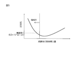
- It is a graph which shows the relationship between the amount of oxygen introduced at the time of forming a light-transmitting conductive layer by a sputtering method, and the specific resistance of the light-transmitting conductive layer formed.
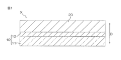
- FIG. 1 is a schematic cross-sectional view of the transparent conductive film X, which is an embodiment of the transparent conductive film of the present invention.
- the transparent conductive film X includes a transparent resin base material 10 and a light-transmitting conductive layer 20 in this order toward one side in the thickness direction D.
- the transparent conductive film X has a shape that spreads in a direction (plane direction) orthogonal to the thickness direction D.
- the transmissive conductive film X is an element provided in a touch sensor device, a light control element, a photoelectric conversion element, a heat ray control member, an antenna member, an electromagnetic wave shield member, a heater member, a lighting device, an image display device, and the like.
- the transparent resin base material 10 includes the resin film 11 and the functional layer 12 in this order toward one side in the thickness direction D.
- the transparent resin base material 10 has a shape that spreads in a direction (plane direction) orthogonal to the thickness direction D.
- the transparent resin base material 10 extends in the in-plane first direction orthogonal to the thickness direction D, and extends in the in-plane second direction orthogonal to each of the thickness direction D and the in-plane first direction. Extend.
- the transparent resin base material 10 has an elongated shape that is long in the first in-plane direction.
- the in-plane first direction is the resin flow direction (MD direction) in the manufacturing process of the resin film 11 contained in the transparent resin base material 10, and the in-plane second direction is the resin flow direction. And the width direction (TD direction) orthogonal to each of the thickness direction D.
- the in-plane first direction is the direction in which the heating dimensional change rate (maximum heat shrinkage rate) of the transparent resin base material 10 is maximum
- the in-plane second direction is the in-plane first direction. It is a direction orthogonal to each of the one direction and the thickness direction D.
- the direction in which the heating dimensional change rate of the transparent resin base material 10 is maximum is the axial direction in increments of 15 ° from the reference axis with the axis extending in an arbitrary direction in the transparent resin base material 10 as the reference axis (0 °). It can be obtained by measuring the dimensional change rate before and after heating.
- a suitable temperature can be set according to the heat resistant temperature of the resin film 11.
- PET polyethylene terephthalate
- a heating temperature of, for example, 150 ° C. can be adopted, and when the resin film 11 is a cycloolefin polymer, a heating temperature of, for example, 110 ° C. can be adopted.
- the heating time is, for example, 1 hour.
- the resin film 11 is a transparent resin film having flexibility.
- the resin film 11 has a shape that spreads in a direction (plane direction) orthogonal to the thickness direction D. Specifically, the resin film 11 extends in the in-plane first direction orthogonal to the thickness direction D, and extends in the in-plane second direction orthogonal to each of the thickness direction D and the in-plane first direction.
- the resin film 11 has an elongated shape that is long in the first in-plane direction.
- the in-plane first direction is the above-mentioned MD direction
- the in-plane second direction is the above-mentioned TD direction.
- Examples of the material of the resin film 11 include polyester resin, polyolefin resin, acrylic resin, polycarbonate resin, polyether sulfone resin, polyarylate resin, melamine resin, polyamide resin, polyimide resin, cellulose resin, and polystyrene resin.
- Examples of the polyester resin include polyethylene terephthalate (PET), polybutylene terephthalate, and polyethylene naphthalate.
- Polyolefin resins include, for example, polyethylene, polypropylene, and cycloolefin polymers.
- Examples of the acrylic resin include polymethacrylate.
- polyester resin is preferably used, and PET is more preferably used.
- the surface of the resin film 11 on the functional layer 12 side may be surface-modified.
- Examples of the surface modification treatment include corona treatment, plasma treatment, ozone treatment, primer treatment, glow treatment, and coupling agent treatment.
- the thickness of the resin film 11 is preferably 1 ⁇ m or more, more preferably 10 ⁇ m or more, and further preferably 30 ⁇ m or more.
- the thickness of the resin film 11 is preferably 300 ⁇ m or less, more preferably 200 ⁇ m or less, still more preferably 100 ⁇ m or less, and particularly preferably 75 ⁇ m or less.
- the total light transmittance (JIS K 7375-2008) of the resin film 11 is preferably 60% or more, more preferably 80% or more, still more preferably 85% or more.
- the transparent conductive film X is provided in the touch sensor device, the dimming element, the photoelectric conversion element, the heat ray control member, the antenna member, the electromagnetic wave shield member, the heater member, the lighting device, the image display device, and the like. It is suitable for ensuring the transparency required for the transparent conductive film X.
- the total light transmittance of the resin film 11 is, for example, 100% or less.
- the functional layer 12 is located on one surface of the thickness direction D of the resin film 11. Further, in the present embodiment, the functional layer 12 is a hard coat layer for preventing scratches from being formed on the exposed surface (upper surface in FIG. 1) of the light-transmitting conductive layer 20.
- the hard coat layer is a cured product of a curable resin composition.
- the resin contained in the curable resin composition include polyester resin, acrylic resin, urethane resin, amide resin, silicone resin, epoxy resin, and melamine resin.
- the curable resin composition include an ultraviolet curable resin composition and a thermosetting resin composition.
- an ultraviolet curable resin composition is preferably used from the viewpoint of helping to improve the production efficiency of the transparent conductive film X because it can be cured without heating at a high temperature.
- Specific examples of the ultraviolet curable resin composition include the composition for forming a hard coat layer described in JP-A-2016-179686.
- the surface of the functional layer 12 on the light-transmitting conductive layer 20 side may be surface-modified.
- the surface modification treatment include corona treatment, plasma treatment, ozone treatment, primer treatment, glow treatment, and coupling agent treatment.
- the thickness of the functional layer 12 as the hard coat layer is preferably 0.1 ⁇ m or more, more preferably 0.5 ⁇ m or more, and further preferably 1 ⁇ m or more. Such a configuration is suitable for exhibiting sufficient scratch resistance in the light-transmitting conductive layer 20.
- the thickness of the functional layer 12 as the hard coat layer is preferably 10 ⁇ m or less, more preferably 5 ⁇ m or less, and further preferably 3 ⁇ m or less from the viewpoint of ensuring the transparency of the functional layer 12.
- the thickness of the transparent resin base material 10 is preferably 1 ⁇ m or more, more preferably 10 ⁇ m or more, still more preferably 15 ⁇ m or more, and particularly preferably 30 ⁇ m or more.
- the thickness of the transparent resin base material 10 is preferably 310 ⁇ m or less, more preferably 210 ⁇ m or less, still more preferably 110 ⁇ m or less, and particularly preferably 80 ⁇ m or less.
- the total light transmittance (JIS K 7375-2008) of the transparent resin base material 10 is preferably 60% or more, more preferably 80% or more, still more preferably 85% or more.
- the total light transmittance of the transparent resin base material 10 is, for example, 100% or less.
- the transparent conductive film X does not include a glass base material.
- the transparent resin base material 10 is not adjacent to the glass base material.
- the light-transmitting conductive layer 20 is located on one surface of the thickness direction D of the resin film 11.
- the light-transmitting conductive layer 20 is a crystalline film having both light-transmitting property and conductivity.
- the light-transmitting conductive layer 20 is a layer formed of a light-transmitting conductive material.
- the light-transmitting conductive material contains, for example, a conductive oxide as a main component.
- the conductive oxide for example, at least one kind of metal selected from the group consisting of In, Sn, Zn, Ga, Sb, Ti, Si, Zr, Mg, Al, Au, Ag, Cu, Pd and W.
- a metal oxide containing a semi-metal can be mentioned.
- the conductive oxide include an indium-containing conductive oxide and an antimony-containing conductive oxide.
- the indium-containing conductive oxide include indium tin oxide composite oxide (ITO), indium zinc composite oxide (IZO), indium gallium composite oxide (IGO), and indium gallium zinc composite oxide (IGZO). Be done.
- the antimony-containing conductive oxide include antimony tin composite oxide (ATO).
- an indium-containing conductive oxide is preferably used as the conductive oxide, and ITO is more preferably used.
- the ITO may contain a metal or a semimetal other than In and Sn in an amount less than the respective contents of In and Sn.
- the ratio of the tin oxide content to the total content of indium (In 2 O 3 ) and tin oxide (SnO 2) in the ITO is preferably 0.1% by mass. As mentioned above, it is more preferably 3% by mass or more, further preferably 5% by mass or more, and particularly preferably 7% by mass or more.
- the ratio of the number of tin atoms to the number of indium atoms (number of tin atoms / number of indium atoms) in the ITO used is preferably 0.001 or more, more preferably 0.03 or more, still more preferably 0.05 or more, and particularly preferably 0.05 or more. It is 0.07 or more.
- the ratio of the tin oxide content to the total content of indium oxide (In 2 O 3 ) and tin oxide (SnO 2 ) in the ITO used is preferably 15% by mass or less, more preferably 13% by mass or less. More preferably, it is 12% by mass or less.
- the ratio of the number of tin atoms to the number of indium atoms in the ITO used is preferably 0.16 or less, more preferably 0.14 or less, still more preferably 0.13 or less.
- the ratio of the number of tin atoms to the number of indium atoms in ITO can be obtained, for example, by specifying the abundance ratio of indium atoms and tin atoms in the object to be measured by X-ray Photoelectron Spectroscopy.
- the above-mentioned content ratio of tin oxide in ITO is obtained from, for example, the abundance ratio of the indium atom and the tin atom thus specified.
- the above-mentioned content ratio of tin oxide in ITO may be judged from the tin oxide (SnO 2) content ratio of the ITO target used at the time of sputtering film formation.
- the light-transmitting conductive layer 20 may contain a rare gas atom.
- Rare gas atoms include, for example, argon (Ar), krypton (Kr), and xenon (Xe).
- the rare gas atom in the light transmissive conductive layer 20 is derived from the rare gas atom used as the sputtering gas in the sputtering method described later for forming the light transmissive conductive layer 20.
- the light-transmitting conductive layer 20 is a film (sputtered film) formed by a sputtering method.
- the content ratio of rare gas atoms in the light transmissive conductive layer 20 is preferably 1.2 atomic% or less, more preferably 1. 1 atomic% or less, more preferably 1.0 atomic% or less, even more preferably 0.8 atomic% or less, still more preferably 0.5 atomic% or less, still more preferably 0.4 atomic% or less, very preferably. It is 0.3 atomic% or less, particularly preferably 0.2 atomic% or less.
- the amorphous light-transmitting conductive layer (the light-transmitting conductive layer 20'described later) is crystallized by heating to form the light-transmitting conductive layer 20. It is suitable for forming large crystal grains that realize good crystal growth, and therefore suitable for obtaining a light-transmitting conductive layer 20 having low resistance (the larger the crystal grains in the light-transmitting conductive layer 20). , The resistance of the light-transmitting conductive layer 20 is low). Further, the light-transmitting conductive layer 20 includes a region in which the noble gas atom content ratio is, for example, 0.0001 atomic% or more, in at least a part of the thickness direction D. The noble gas atom content ratio in the light transmissive conductive layer 20 is preferably 0.0001 atomic% or more in the entire area in the thickness direction D.
- the presence or absence and content of rare gas atoms such as Kr in the light transmissive conductive layer 20 are identified by, for example, Rutherford Backscattering Spectrometry, which will be described later with respect to Examples.
- the presence or absence of rare gas atoms such as Kr in the light transmissive conductive layer 20 is identified by, for example, fluorescent X-ray analysis described later with respect to Examples.
- the noble gas atom content cannot be quantified because it is not above the detection limit value (lower limit value), and according to the fluorescent X-ray analysis, the noble gas atom.
- the existence of is identified, it is determined that the light-transmitting conductive layer includes a region in which the content ratio of rare gas atoms such as Kr is 0.0001 atomic% or more.
- the light-transmitting conductive layer 20 preferably does not contain Xe.
- the light-transmitting conductive layer 20 is preferably a rare gas atom. It contains Kr, more preferably only Kr.
- the configuration suitable for forming large crystal grains in the light-transmitting conductive layer 20 is suitable for realizing low resistance of the light-transmitting conductive layer 20.
- the configuration suitable for forming large crystal grains in the light-transmitting conductive layer 20 is suitable for reducing the net compressive residual stress in the light-transmitting conductive layer 20 to be formed.
- the light-transmitting conductive layer 20 has a Kr content of preferably 1.0 atomic% or less, more preferably 0.7 atomic% or less, still more preferably 0.5 atomic% or less, and even more preferably 0.3.
- the Kr content ratio of the region is, for example, 0.0001 atomic% or more.
- the light-transmitting conductive layer 20 satisfies such a Kr content ratio in the entire area in the thickness direction D.
- the content ratio of Kr in the light transmissive conductive layer 20 is preferably 1.0 atomic% or less, more preferably 0.7 atomic% or less, and further preferably 0. It is 5 atomic% or less, more preferably 0.3 atomic% or less, very preferably 0.2 atomic% or less, and particularly preferably less than 0.1 atomic%.
- the content ratio of Kr in the light-transmitting conductive layer 20 may be non-uniform in the thickness direction D.
- the Kr content may gradually increase or decrease as the distance from the transparent resin base material 10 increases.
- the partial region where the Kr content ratio gradually increases as the distance from the transparent resin base material 10 increases is located on the transparent resin base material 10 side, and the Kr content ratio gradually decreases as the distance from the transparent resin base material 10 increases.
- the partial region may be located on the opposite side of the transparent resin base material 10.
- the partial region where the Kr content ratio gradually decreases as the distance from the transparent resin base material 10 increases is located on the transparent resin base material 10 side, and the Kr content ratio gradually increases as the distance from the transparent resin base material 10 increases.
- the partial region may be located on the opposite side of the transparent resin base material 10.
- the light-transmitting conductive layer 20 may contain Kr in a part of the thickness direction D.
- FIG. 2A shows a case where the light-transmitting conductive layer 20 includes the first region 21 and the second region 22 in this order from the transparent resin base material 10 side.
- the first region 21 contains Kr.
- the second region 22 does not contain Kr, and contains, for example, a noble gas atom other than Kr.
- FIG. 2B shows a case where the light-transmitting conductive layer 20 includes the second region 22 and the first region 21 in this order from the transparent resin base material 10 side.
- FIG. 2A shows a case where the light-transmitting conductive layer 20 includes the first region 21 and the second region 22 in this order from the transparent resin base material 10 side.
- the first region 21 contains Kr.
- the second region 22 does not contain Kr, and contains, for example, a noble gas atom other than Kr.
- FIG. 2B shows a case where the light-transmitting conductive layer 20 includes the
- the boundary between the first region 21 and the second region 22 is drawn by a virtual line, the first region 21 and the second region 22 have a composition other than the rare gas atom whose content is very small. When they are not significantly different, the boundary between the first region 21 and the second region 22 may not be clearly discriminated.
- the light-transmitting conductive layer 20 has a first region 21 (Kr-containing region) and a second region 22 (Kr-free region). ) Is included in this order from the transparent resin base material 10 side.
- the ratio of the thickness of the first region 21 to the total thickness of the first region 21 and the second region 22 is preferably 1%. As mentioned above, it is more preferably 20% or more, further preferably 30% or more, further preferably 40% or more, and particularly preferably 50% or more. The same ratio is less than 100%.
- the ratio of the thickness of the second region 22 to the total thickness of the first region 21 and the second region 22 is preferably 99% or less, more preferably 80% or less, still more preferably 70% or less, and further. It is preferably 60% or less, particularly preferably 50% or less.
- the configuration regarding the ratio of the thickness of each of the first region 21 and the second region 22 is the compression in the light-transmitting conductive layer 20. It is preferable from the viewpoint of achieving both reduction of residual stress and reduction of specific resistance.
- the content ratio of Kr in the first region 21 is preferably 1.0 atomic% or less, more preferably 0.7 atomic% or less, still more preferably 0. It is 5 atomic% or less, more preferably 0.3 atomic% or less, more preferably 0.2 atomic% or less, and particularly preferably less than 0.1 atomic%. Such a configuration is suitable for realizing the above-mentioned low resistance and reduction of compressive residual stress in the light-transmitting conductive layer 20. Further, the content ratio of Kr in the first region 21 is, for example, 0.0001 atomic% or more in the entire area of the thickness direction D of the first region 21.
- the content ratio of Kr in the first region 21 may be non-uniform in the thickness direction D of the first region 21.
- the Kr content ratio may gradually increase or decrease as the distance from the transparent resin base material 10 increases.
- the partial region where the Kr content ratio gradually increases as the distance from the transparent resin base material 10 increases is located on the transparent resin base material 10 side, and the distance from the transparent resin base material 10 increases.
- the partial region where the Kr content ratio gradually decreases may be located on the opposite side of the transparent resin base material 10.
- the partial region where the Kr content ratio gradually decreases as the distance from the transparent resin base material 10 increases is located on the transparent resin base material 10 side, and the distance from the transparent resin base material 10 increases.
- the partial region where the Kr content ratio gradually increases may be located on the opposite side of the transparent resin base material 10.
- the thickness of the light-transmitting conductive layer 20 is, for example, 10 nm or more.
- the thickness of the light-transmitting conductive layer 20 is preferably more than 40 nm, more preferably 100 nm or more, still more preferably 110 nm or more, and further preferably 120 nm or more.
- Such a configuration is suitable for reducing the resistance of the light-transmitting conductive layer 20.
- the thickness of the light-transmitting conductive layer 20 is, for example, 1000 nm or less, preferably less than 300 nm, more preferably 250 nm or less, further preferably 200 nm or less, still more preferably 160 nm or less, and particularly preferably less than 150 nm. It is preferably 148 nm or less.
- Such a configuration is suitable for suppressing the warp of the transparent conductive film X.
- the surface resistance of the light transmissive conductive layer 20 is, for example, 200 ⁇ / ⁇ or less, preferably 100 ⁇ / ⁇ or less, more preferably 50 ⁇ / ⁇ or less, still more preferably 15 ⁇ / ⁇ or less, still more preferably 15 ⁇ / ⁇ or less, particularly. It is preferably 13 ⁇ / ⁇ or less.
- the surface resistance of the light-transmitting conductive layer 20 is, for example, 1 ⁇ / ⁇ or more.
- These configurations relating to surface resistance include a transparent conductive film X in a touch sensor device, a dimming element, a photoelectric conversion element, a heat ray control member, an antenna member, an electromagnetic wave shield member, a heater member, a lighting device, an image display device, and the like. When provided, it is suitable for ensuring the low resistance required for the light-transmitting conductive layer 20.
- the surface resistance can be measured by the 4-terminal method based on JIS K7194.
- the specific resistance of the light transmissive conductive layer 20 is, for example, 2.5 ⁇ 10 -4 ⁇ ⁇ cm or less, preferably less than 2.2 ⁇ 10 -4 ⁇ ⁇ cm, more preferably 2 ⁇ 10 -4 ⁇ ⁇ cm or less. It is more preferably 1.9 ⁇ 10 -4 ⁇ ⁇ cm or less, and particularly preferably 1.8 ⁇ 10 -4 ⁇ ⁇ cm or less.
- the specific resistance of the light transmissive conductive layer 20 is preferably 0.1 ⁇ 10 -4 ⁇ ⁇ cm or more, more preferably 0.5 ⁇ 10 -4 ⁇ ⁇ cm or more, and further preferably 1.0 ⁇ 10 -4. ⁇ ⁇ cm or more.
- Specific resistance examples include a transparent conductive film X in a touch sensor device, a dimming element, a photoelectric conversion element, a heat ray control member, an antenna member, an electromagnetic wave shield member, a heater member, a lighting device, an image display device, and the like.
- the specific resistance is obtained by multiplying the surface resistance by the thickness.
- the resistivity can be controlled, for example, by adjusting the noble gas atom content ratio in the light-transmitting conductive layer 20 and adjusting various conditions when the light-transmitting conductive layer 20 is sputter-deposited.
- the conditions include, for example, the temperature of the base (transparent resin base material 10 in this embodiment) on which the light transmissive conductive layer 20 is formed, the amount of oxygen introduced into the film forming chamber, the air pressure in the film forming chamber, and the pressure in the film forming chamber.
- the horizontal magnetic field strength on the target can be mentioned.
- the total light transmittance (JIS K 7375-2008) of the light-transmitting conductive layer 20 is preferably 60% or more, more preferably 80% or more, still more preferably 85% or more. Such a configuration is suitable for ensuring transparency in the light-transmitting conductive layer 20. Further, the total light transmittance of the light-transmitting conductive layer 20 is, for example, 100% or less.
- the light-transmitting conductive layer is crystalline can be determined, for example, as follows. First, the light-transmitting conductive layer (in the case of the transparent conductive film X, the light-transmitting conductive layer 20 on the transparent resin base material 10) is immersed in hydrochloric acid having a concentration of 5% by mass at 20 ° C. for 15 minutes. Next, the light-transmitting conductive layer is washed with water and then dried. Next, on the exposed plane of the light-transmitting conductive layer (in the transparent conductive film X, the surface of the light-transmitting conductive layer 20 opposite to the transparent resin base material 10), between a pair of terminals having a separation distance of 15 mm. Measure the resistance (resistance between terminals).
- the light-transmitting conductive layer is crystalline. It can also be determined that the light-transmitting conductive layer is crystalline by observing the presence of crystal grains in the light-transmitting conductive layer in a plan view with a transmission electron microscope.
- the light-transmitting conductive layer 20 has a first compressive residual stress in the in-plane first direction and a second compressive residual stress smaller than the first compressive residual stress in the in-plane second direction. That is, in the light transmissive conductive layer 20, the in-plane first direction orthogonal to the in-plane first direction is more than the compressive residual stress (first in-plane first direction) in at least one direction (in-plane first direction). The compressive residual stress in the two directions (second compressive residual stress) is small.
- the in-plane first direction is the above-mentioned MD direction
- the in-plane second direction is the above-mentioned TD direction
- the in-plane first direction is orthogonal to the thickness direction D.
- the in-plane second direction is orthogonal to each of the thickness direction D and the in-plane first direction).
- the first compressive residual stress is preferably 620 MPa or less, more preferably 600 MPa or less, and further preferably 550 MPa or less.
- the first compressive residual stress is, for example, 1 MPa or more.
- the second compressive residual stress is preferably 530 MPa or less, more preferably 500 MPa or less, still more preferably 450 MPa or less, as long as it is smaller than the first compressive residual stress.
- the second compressive residual stress is, for example, 1 MPa or more as long as it is smaller than the first compressive residual stress.
- the ratio of the second compressive residual stress to the first compressive residual stress is 0.82 or less, preferably 0.8 or less.
- the ratio is, for example, 0.1 or more, preferably 0.3 or more, and more preferably 0.4 or more.
- a configuration in which the second compressive residual stress in the in-plane second direction (TD direction in the present embodiment) is smaller than the first compressive residual stress in the in-plane first direction (MD direction in this embodiment) is a high crystal. Helps to achieve stability.
- the transparent conductive film X is manufactured as follows, for example.
- the resin film 11 is prepared.
- the functional layer 12 is formed on one surface of the resin film 11 in the thickness direction D.
- the transparent resin base material 10 is produced by forming the functional layer 12 on the resin film 11.
- the above-mentioned functional layer 12 as a hard coat layer can be formed by applying a curable resin composition on a resin film 11 to form a coating film, and then curing the coating film.
- the curable resin composition contains an ultraviolet-forming resin
- the coating film is cured by ultraviolet irradiation.
- the curable resin composition contains a thermosetting resin
- the coating film is cured by heating.
- the exposed surface of the functional layer 12 formed on the resin film 11 is surface-modified, if necessary.
- plasma treatment for example, argon gas is used as the inert gas.
- the discharge power in the plasma processing is, for example, 10 W or more, and for example, 5000 W or less.
- an amorphous light-transmitting conductive layer 20' is formed on the transparent resin base material 10 (deposition step). Specifically, a material is formed on the functional layer 12 of the transparent resin base material 10 by a sputtering method to form an amorphous light-transmitting conductive layer 20'.
- the light-transmitting conductive layer 20' is an amorphous film having both light-transmitting property and conductivity (the light-transmitting conductive layer 20'is a crystalline light-transmitting conductivity by heating in a crystallization step described later. Converted to layer 20).
- the sputtering film forming apparatus capable of carrying out the film forming process by the roll-to-roll method.
- a roll-to-roll type sputter film forming apparatus is used in the production of the transparent conductive film X, the long transparent resin base material 10 is run from the feeding roll to the winding roll provided in the apparatus to be transparent. A material is formed on the resin base material 10 to form a light-transmitting conductive layer 20'.
- a sputtering film forming apparatus provided with one film forming chamber may be used, or sputtering forming provided with a plurality of film forming chambers sequentially arranged along a traveling path of the transparent resin base material 10.
- a film device may be used (when the light transmissive conductive layer 20'including the above-mentioned first region 21 and second region 22 is formed, a sputter film forming apparatus including two or more film forming chambers). Use).
- a sputtering gas in the sputtering method, specifically, while introducing a sputtering gas (inert gas) into the film forming chamber provided in the sputtering film forming apparatus under vacuum conditions, a negative voltage is applied to the target arranged on the cathode in the film forming chamber. Is applied. As a result, a glow discharge is generated to ionize gas atoms, the gas ions collide with the target surface at high speed, the target material is ejected from the target surface, and the ejected target material is used as the functional layer 12 in the transparent resin base material 10. Deposit on top.
- a sputtering gas in the film forming chamber provided in the sputtering film forming apparatus under vacuum conditions
- the above-mentioned conductive oxide with respect to the light-transmitting conductive layer 20 is used, preferably an indium-containing conductive oxide is used, and more preferably ITO is used. Used.
- the ratio of the tin oxide content to the total content of tin oxide and indium oxide in the ITO is preferably 0.1% by mass or more, more preferably 1% by mass or more, still more preferably 3% by mass. % Or more, more preferably 5% by mass or more, particularly preferably 7% by mass or more, and preferably 15% by mass or less, more preferably 13% by mass or less, still more preferably 12% by mass or less.
- the sputtering method is preferably a reactive sputtering method.
- a reactive gas is introduced into the film forming chamber in addition to the sputtering gas.
- the light-transmitting conductive layer 20'containing a rare gas atom is formed over the entire area in the thickness direction D (first case), it is introduced into one or more film forming chambers provided in the sputtering film forming apparatus.
- the gas contains a sputtering gas and oxygen as a reactive gas.
- a noble gas atom is used in this embodiment. Examples of the noble gas atom include Ar, Kr, and Xe, and Kr is preferably used.
- the sputtering gas contains an inert gas other than Kr, the content ratio is preferably 80% by volume or less, more preferably 50% by volume or less.
- the gas introduced into the film forming chamber for forming the first region 21 is , Kr as a sputtering gas and oxygen as a reactive gas.
- the sputtering gas may contain an inert gas other than Kr.
- the content ratio of the inert gas other than Kr in the sputtering gas is the same as the content ratio described above in the first case.
- the gas introduced into the film forming chamber for forming the second region 22 contains an inert gas other than Kr as a sputtering gas and oxygen as a reactive gas.
- the inert gas other than Kr include Ar and Xe, and Ar is preferably used.
- the ratio of the amount of oxygen introduced to the total amount of sputtering gas and oxygen introduced into the film forming chamber in the reactive sputtering method is, for example, 0.01 flow rate% or more, and for example, 15 flow rate% or less.
- the air pressure in the film formation chamber during film formation (sputter film formation) by the sputtering method is, for example, 0.02 Pa or more, and for example, 1 Pa or less.
- the temperature of the transparent resin base material 10 during the sputtering film formation is, for example, 100 ° C. or lower. In order to suppress outgas from the transparent resin base material 10 and thermal expansion of the transparent resin base material 10 during sputter film formation, it is preferable to cool the transparent resin base material 10. The suppression of outgas and the suppression of thermal expansion are useful for achieving high crystal stability in the light-transmitting conductive layer 20. From this point of view, the temperature of the transparent resin base material 10 during the sputtering film formation is preferably 20 ° C. or lower, more preferably 10 ° C. or lower, still more preferably 5 ° C. or lower, particularly preferably 0 ° C. or lower, and For example, ⁇ 50 ° C. or higher, preferably ⁇ 20 ° C. or higher, more preferably ⁇ 10 ° C. or higher, still more preferably ⁇ 7 ° C. or higher.
- Examples of the power supply for applying a voltage to the target include a DC power supply, an AC power supply, an MF power supply, and an RF power supply.
- a DC power source and an RF power source may be used in combination.
- the absolute value of the discharge voltage during the sputtering film formation is, for example, 50 V or more, and for example, 500 V or less.
- the light-transmitting conductive layer 20 is converted (crystallized) from amorphous to crystalline by heating (crystallization step).
- the heating means include an infrared heater and an oven (heat medium heating type oven, hot air heating type oven).
- the heating environment may be either a vacuum environment or an atmospheric environment.
- heating is carried out in the presence of oxygen.
- the heating temperature is, for example, 100 ° C. or higher, preferably 120 ° C. or higher, from the viewpoint of ensuring a high crystallization rate.
- the heating temperature is, for example, less than 200 ° C., preferably 180 ° C. or lower, more preferably 170 ° C.
- the heating time is, for example, 10 hours or less, preferably 200 minutes or less, more preferably 90 minutes or less, still more preferably 60 minutes or less, and for example, 1 minute or more, preferably 5 minutes or more.
- the transparent resin base material 10 shrinks.
- the configuration in which the light-transmitting conductive layer 20 contains Kr is suitable for appropriately shrinking the light-transmitting conductive layer 20 on the shrinkable transparent resin base material 10 in the state after returning to room temperature (light).
- the preferable Kr content ratio in the permeable conductive layer 20 is as described above).
- the shrinkage of the light-transmitting conductive layer 20 after returning to room temperature helps to reduce the compressive residual stress in the light-transmitting conductive layer 20.
- the transparent conductive film X is manufactured.
- the light-transmitting conductive layer 20 in the transparent conductive film X may be patterned as schematically shown in FIG.
- the light-transmitting conductive layer 20 can be patterned by etching the light-transmitting conductive layer 20 through a predetermined etching mask.
- the patterning of the light-transmitting conductive layer 20 may be carried out before the above-mentioned crystallization step or after the crystallization step.
- the patterned light-transmitting conductive layer 20 functions as, for example, a wiring pattern.
- the light-transmitting conductive layer 20 on the transparent resin base material 10 has the first compressive residual stress in the in-plane first direction, and the in-plane second direction (in-plane). It has a second compressive residual stress that is smaller than the first compressive residual stress (perpendicular to the first direction), and the ratio of the second compressive residual stress to the first compressive residual stress is 0.82 or less, preferably 0.8. It is as follows. Such a configuration is suitable for achieving high crystal stability in the light-transmitting conductive layer 20.
- the transparent conductive film X in which the second compressive residual stress in the in-plane second direction is smaller than the first compressive residual stress in the in-plane first direction to this extent is as described above at a relatively low temperature.
- the transparent conductive film X in which the crystalline light-transmitting conductive layer 20 is formed through the crystallization process is also suitable for suppressing the subsequent resistance value fluctuation of the light-transmitting conductive layer 20. Specifically, it is as shown in Examples and Comparative Examples described later.
- the functional layer 12 may be an adhesion improving layer for realizing high adhesion of the light-transmitting conductive layer 20 to the transparent resin base material 10.
- the configuration in which the functional layer 12 is an adhesion improving layer is suitable for ensuring the adhesion between the transparent resin base material 10 and the light-transmitting conductive layer 20.
- the functional layer 12 may be an index-matching layer for adjusting the reflectance of the surface of the transparent resin base material 10 (one surface in the thickness direction D).
- the configuration in which the functional layer 12 is the refractive index adjusting layer makes it difficult to visually recognize the pattern shape of the light-transmitting conductive layer 20 when the light-transmitting conductive layer 20 on the transparent resin base material 10 is patterned. Suitable for.
- the functional layer 12 may be a peeling functional layer for practically peeling the light-transmitting conductive layer 20 from the transparent resin base material 10.
- the configuration in which the functional layer 12 is a peeling functional layer is suitable for peeling the light-transmitting conductive layer 20 from the transparent resin base material 10 and transferring the light-transmitting conductive layer 20 to another member.
- the functional layer 12 may be a composite layer in which a plurality of layers are connected in the thickness direction D.
- the composite layer preferably includes two or more layers selected from the group consisting of a hard coat layer, an adhesion improving layer, a refractive index adjusting layer, and a peeling functional layer.
- Such a configuration is suitable for complex expression of the above-mentioned functions of each selected layer in the functional layer 12.
- the functional layer 12 includes an adhesion improving layer, a hard coat layer, and a refractive index adjusting layer on the resin film 11 in this order toward one side in the thickness direction D.
- the functional layer 12 includes a peeling functional layer, a hard coat layer, and a refractive index adjusting layer on the resin film 11 in this order toward one side in the thickness direction D.
- the transparent conductive film X is used in a state of being fixed to the article and, if necessary, the light transmissive conductive layer 20 being patterned.
- the transparent conductive film X is attached to the article via, for example, a fixing functional layer.
- the transparent resin base material 10 of the transparent conductive film X is not adjacent to the glass base material, but there is an adhesive, an adhesive, or the like between the transparent resin base material 10 and the glass base material.
- An anchoring functional layer may intervene.
- Examples of articles include elements, members, and devices. That is, examples of the article with a transparent conductive film include an element with a transparent conductive film, a member with a transparent conductive film, and a device with a transparent conductive film.
- Examples of the element include a dimming element and a photoelectric conversion element.
- Examples of the dimming element include a current-driven dimming element and an electric field-driven dimming element.
- Examples of the current-driven dimming element include an electrochromic (EC) dimming element.
- Examples of the electric field drive type dimming element include a PDLC (polymer dispersed liquid crystal) dimming element, a PNLC (polymer network liquid crystal) dimming element, and an SPD (suspended particle device) dimming element.
- Examples of the photoelectric conversion element include a solar cell and the like.
- Examples of the solar cell include an organic thin-film solar cell and a dye-sensitized solar cell.
- Examples of the member include an electromagnetic wave shield member, a heat ray control member, a heater member, and an antenna member.
- Examples of the device include a touch sensor device, a lighting device, and an image display device.
- the articles with the transparent conductive film are suitable for realizing high crystal stability in the light-transmitting conductive layer 20 of the transparent conductive film X provided therein, stable characteristics are exhibited in the light-transmitting conductive layer 20. Suitable for.
- the fixing functional layer examples include an adhesive layer and an adhesive layer.
- the material of the fixing function layer any material having transparency and exhibiting the fixing function can be used without particular limitation.
- the fixing functional layer is preferably formed of a resin.
- the resin include acrylic resin, silicone resin, polyester resin, polyurethane resin, polyamide resin, polyvinyl ether resin, vinyl acetate / vinyl chloride copolymer, modified polyolefin resin, epoxy resin, fluororesin, natural rubber, and synthetic rubber. Be done.
- Acrylic resin is preferable as the resin because it exhibits adhesive properties such as cohesiveness, adhesiveness, and appropriate wettability, is excellent in transparency, and is excellent in weather resistance and heat resistance.
- a corrosion inhibitor may be added to the fixing functional layer (resin forming the fixing functional layer) in order to suppress corrosion of the light-transmitting conductive layer 20.
- a migration inhibitor (for example, a material disclosed in Japanese Patent Application Laid-Open No. 2015-0222397) may be added to the fixing functional layer (resin forming the fixing functional layer) in order to suppress migration of the light-transmitting conductive layer 20. good.
- the fixing functional layer (resin forming the fixing functional layer) may be blended with an ultraviolet absorber in order to suppress deterioration of the article when it is used outdoors. Examples of the ultraviolet absorber include benzophenone compounds, benzotriazole compounds, salicylic acid compounds, oxalic acid anilides compounds, cyanoacrylate compounds, and triazine compounds.
- the light-transmitting conductive layer 20 (the light-transmitting conductive layer 20 after patterning) is formed in the transparent conductive film X. (Including) is exposed.
- the cover layer may be arranged on the exposed surface of the light-transmitting conductive layer 20.
- the cover layer is a layer that covers the light-transmitting conductive layer 20, and can improve the reliability of the light-transmitting conductive layer 20 and suppress functional deterioration due to damage to the light-transmitting conductive layer 20.
- Such a cover layer is preferably formed of a dielectric material, more preferably of a composite material of a resin and an inorganic material.
- Examples of the resin include the above-mentioned resins for the fixing functional layer.
- Examples of the inorganic material include inorganic oxides and fluorides.
- Examples of the inorganic oxide include silicon oxide, titanium oxide, niobium oxide, aluminum oxide, zirconium dioxide, and calcium oxide.
- Examples of the fluoride include magnesium fluoride.
- the cover layer may contain the above-mentioned corrosion inhibitor, migration inhibitor, and ultraviolet absorber.
- the present invention will be specifically described below with reference to examples.
- the present invention is not limited to the examples.
- the specific numerical values such as the compounding amount (content), the physical property value, the parameter, etc. described below are the compounding amounts corresponding to them described in the above-mentioned "mode for carrying out the invention”. It can be replaced with an upper limit (numerical value defined as “less than or equal to” or “less than”) or a lower limit (numerical value defined as "greater than or equal to” or “greater than or equal to”) such as content), physical property value, and parameter.
- Example 1 An ultraviolet curable resin containing an acrylic resin was applied to one surface of a long PET film (thickness 50 ⁇ m, manufactured by Toray Industries, Inc.) as a resin film to form a coating film. Next, the coating film was cured by ultraviolet irradiation to form a hard coat layer (thickness 2 ⁇ m). In this way, a transparent resin base material having a resin film and a hard coat layer as a functional layer was produced (in the direction of maximum shrinkage after heat treatment of this transparent base material at 165 ° C. for 1 hour.
- the heat shrinkage rate (maximum heat shrinkage rate, heat shrinkage rate in the MD direction in this example) of the transparent substrate is 0.63%).
- an amorphous light-transmitting conductive layer having a thickness of 130 nm was formed on the hard coat layer of the transparent resin base material by the reactive sputtering method (deposition step).
- a sputtering film forming apparatus DC magnetron sputtering apparatus capable of carrying out a film forming process by a roll-to-roll method was used.
- the conditions for sputter film formation in this example are as follows.
- a sintered body of indium oxide and tin oxide (tin oxide concentration was 10% by mass) was used.
- a DC power supply was used as the power supply for applying the voltage to the target.
- the horizontal magnetic field strength on the target was 90 mT.
- the film formation temperature (the temperature of the transparent resin base material on which the light-transmitting conductive layer is laminated) was set to ⁇ 5 ° C. Further, after the film forming chamber is evacuated until the ultimate vacuum degree in the film forming chamber of the apparatus reaches 0.8 ⁇ 10 -4 Pa, Kr as a sputtering gas and Kr as a reactive gas are used in the film forming chamber. Oxygen was introduced, and the air pressure in the film forming chamber was set to 0.2 Pa.
- the ratio of the oxygen introduction amount to the total introduction amount of Kr and oxygen introduced into the film forming chamber is about 2.5 flow rate%, and the oxygen introduction amount is the specific resistance-oxygen introduction amount curve as shown in FIG.
- the value of the specific resistance of the formed film was adjusted to be 6.5 ⁇ 10 -4 ⁇ ⁇ cm within the region R of.
- the resistivity-oxygen introduction amount curve shown in FIG. 5 shows the specific resistance of the light-transmitting conductive layer when the light-transmitting conductive layer is formed by the reactive sputtering method under the same conditions as above except for the oxygen introduction amount.
- the dependence on the amount of oxygen introduced can be investigated and created in advance.
- the light-transmitting conductive layer on the transparent resin substrate was crystallized by heating in a hot air oven (crystallization step).
- the heating temperature was 165 ° C. and the heating time was 1 hour.
- the transparent conductive film of Example 1 was produced.
- the light-transmitting conductive layer (thickness 130 nm, crystalline) of the transparent conductive film of Example 1 is composed of a single Kr-containing ITO layer.
- Example 2 The transparent conductivity of Example 2 is the same as that of the transparent conductive film of Example 1, except that a part of the film forming conditions in the film forming step is changed and the heating conditions in the crystallization step are changed.
- a film was made.
- the air pressure in the film forming chamber was set to 0.4 Pa, and the thickness of the light-transmitting conductive layer formed was set to 160 nm.
- the heating temperature was 155 ° C. and the heating time was 2 hours.
- the light-transmitting conductive layer (thickness 160 nm, crystalline) of the transparent conductive film of Example 2 is composed of a single Kr-containing ITO layer.
- Example 3 In the film forming step, a first sputter film formation for forming a first region (thickness 50 nm) of a light-transmitting conductive layer on a transparent resin base material and a second region of a light-transmitting conductive layer on the first region.
- the transparent conductive film of Example 3 was produced in the same manner as the transparent conductive film of Example 1 except that the second sputter film forming (thickness 80 nm) was sequentially carried out.
- the conditions for the first sputter film formation in this example are as follows.
- a target a sintered body of indium oxide and tin oxide (tin oxide concentration was 10% by mass) was used.
- a DC power supply was used as the power supply for applying the voltage to the target.
- the horizontal magnetic field strength on the target was 90 mT.
- the film formation temperature was ⁇ 5 ° C.
- Kr is added to the first film forming chamber as a sputtering gas.
- Oxygen as a reactive gas was introduced, and the air pressure in the film forming chamber was set to 0.2 Pa.
- the amount of oxygen introduced into the film forming chamber was adjusted so that the value of the specific resistance of the film to be formed was 6.5 ⁇ 10 -4 ⁇ ⁇ cm.
- the conditions for the second sputter film formation in this example are as follows. After vacuum exhausting the second film forming chamber until the ultimate vacuum degree in the second film forming chamber of the apparatus reaches 0.8 ⁇ 10 -4 Pa, the reaction with Ar as a sputtering gas in the second film forming chamber. Oxygen as a sex gas was introduced, and the air pressure in the film forming chamber was set to 0.4 Pa. In this embodiment, the other conditions in the second sputter film formation are the same as those in the first sputter film formation.
- the transparent conductive film of Example 3 was produced.
- the light-transmitting conductive layer (thickness 130 nm, crystalline) of the transparent conductive film of Example 3 has a first region (thickness 50 nm) composed of a Kr-containing ITO layer and a second region (thickness 50 nm) composed of an Ar-containing ITO layer. With a thickness of 80 nm) in order from the transparent resin base material side.
- the thickness of the first region was set to 50 nm to 66 nm (Example 4), 85 nm (Example 5), or 87 nm (Example 6), and The same procedure as for the transparent conductive film of Example 3 was carried out except that the thickness of the second region was set to 80 nm to 64 nm (Example 4), 45 nm (Example 5), or 38 nm (Example 6).
- Each transparent conductive film of Examples 4 to 6 was prepared.
- the light-transmitting conductive layer (thickness 130 nm, crystalline) of the transparent conductive film of Example 4 has a first region (thickness 66 nm) composed of a Kr-containing ITO layer and a second region (thickness 66 nm) composed of an Ar-containing ITO layer. With a thickness of 64 nm) in order from the transparent resin base material side.
- the light-transmitting conductive layer (thickness 130 nm) of the transparent conductive film of Example 5 has a first region (thickness 85 nm) made of a Kr-containing ITO layer and a second region (thickness 45 nm) made of an Ar-containing ITO layer. ), In order from the transparent resin base material side.
- the light-transmitting conductive layer (thickness 125 nm) of the transparent conductive film of Example 6 has a first region (thickness 87 nm) composed of a Kr-containing ITO layer and a second region (thickness 38 nm) composed of an Ar-containing ITO layer. ), In order from the transparent resin base material side.
- Example 7 A transparent conductive film of Example 7 was produced in the same manner as the transparent conductive film of Example 1 except for the following matters in the sputtering film formation.
- a mixed gas of krypton and argon (Kr90% by volume, Ar10% by volume) was used as the sputtering gas.
- the air pressure in the film forming chamber was set to 0.2 Pa.
- the ratio of the oxygen introduction amount to the total introduction amount of the mixed gas and oxygen introduced into the film forming chamber is about 2.7 flow rate%, and the oxygen introduction amount is such that the value of the specific resistance of the formed film is 5.7 ⁇ . It was adjusted to 10 -4 ⁇ ⁇ cm.
- the light-transmitting conductive film (thickness 130 nm, crystalline) of the transparent conductive film of Example 7 is composed of a single ITO layer containing Kr and Ar.
- the thickness of the light-transmitting conductive layer of each transparent conductive film in Examples 1 to 7 and Comparative Examples 1 and 2 was measured by FE-TEM observation. Specifically, first, a cross-section observation sample of each light-transmitting conductive layer in Examples 1 to 7 and Comparative Examples 1 and 2 was prepared by the FIB microsampling method. In the FIB microsampling method, an FIB device (trade name "FB2200", manufactured by Hitachi) was used, and the acceleration voltage was set to 10 kV. Next, the thickness of the light-transmitting conductive layer in the cross-section observation sample was measured by FE-TEM observation. In the FE-TEM observation, an FE-TEM device (trade name "JEM-2800", manufactured by JEOL) was used, and the acceleration voltage was set to 200 kV.
- FE-TEM observation an FE-TEM device (trade name "JEM-2800", manufactured by JEOL) was used, and the acceleration voltage was set to 200 kV.
- a cross-section observation sample was prepared from the intermediate product before forming the second region on the first region, and the sample was prepared. It was measured by FE-TEM observation of.
- the thickness of the second region of each light-transmitting conductive layer in Examples 3 to 6 was obtained by subtracting the thickness of the first region from the total thickness of each light-transmitting conductive layer in Examples 3 to 6.
- the ratio of the first region in the thickness direction of the light-transmitting conductive layer was 38.5% in Example 3, 50.8% in Example 4, 65.4% in Example 5, and 69. In Example 6. It was 6%.
- the specific resistance of the light-transmitting conductive layer was examined for each of the transparent conductive films of Examples 1 to 7 and Comparative Examples 1 and 2. Specifically, by measuring the surface resistance of the light-transmitting conductive layer by the four-terminal method based on JIS K 7194 (1994), the surface resistance value is multiplied by the thickness of the light-transmitting conductive layer. The specific resistance ( ⁇ ⁇ cm) was determined. The results are listed in Table 1.
- the Kr content (atomic%), Ar content (atomic%), and noble gas atom content (atomic%) are listed in Table 1.
- the detection limit value is the thickness of the light transmissive conductive layer attached to the measurement. It depends on the situation). Therefore, in Table 1, it is shown that the Kr content of the light-transmitting conductive layer is below the detection limit value in the thickness of the same layer. "Specific detection limit value in” (the same applies to the notation of the noble gas atom content).
- the compressive residual stress of the light-transmitting conductive layer (crystalline ITO film) of each of the transparent conductive films of Examples 1 to 7 and Comparative Examples 1 and 2 was indirectly obtained from the crystal lattice strain of the light-transmitting conductive layer. .. Specifically, it is as follows.
- a rectangular measurement sample 50 mm ⁇ 50 mm was cut out from the transparent conductive film.
- the crystal lattice spacing d of the light-transmitting conductive layer in the measurement sample was calculated based on the peak (peak of the (622) plane of ITO) angle 2 ⁇ of the obtained diffraction image and the wavelength ⁇ of the X-ray source. , D was used as the basis for calculating the lattice strain ⁇ .
- the following formula (1) was used for the calculation of d
- the following formula (2) was used for the calculation of ⁇ .
- the above X-ray diffraction measurement was performed for the angles ⁇ formed by the film surface normal and the ITO crystal plane normal at 65 °, 70 °, 75 °, and 85 °, respectively, and the lattice strain ⁇ at each ⁇ was determined. Calculated.
- the angle ⁇ formed by the film surface normal and the ITO crystal plane normal is the axis of rotation in the TD direction (the direction orthogonal to the MD direction in the plane) of the transparent resin base material in the measurement sample (a part of the transparent conductive film). Adjusted by rotating the sample around the center (adjustment of angle ⁇ ).
- the residual stress ⁇ in the in-plane direction of the ITO film was obtained by the following equation (3) from the slope of a straight line plotting the relationship between Sin 2 ⁇ and lattice strain ⁇ .
- the obtained residual stress ⁇ is listed in Table 1 as the first compressive residual stress S 1 (MPa) in the MD direction.
- the above-mentioned adjustment of the angle ⁇ in the X-ray diffraction measurement is performed by rotating the sample around the MD direction (the direction orthogonal to the TD direction in the plane) instead of the TD direction of the transparent resin base material in the measurement sample.
- the second compressive residual stress S 2 (MPa) in the TD direction was derived in the same manner as the first compressive residual stress S 1 except that it was realized by the above. The values are listed in Table 1. Table 1 also lists the ratio of the first compressive residual stress S 1 to the second compressive residual stress S 2 (S 1 / S 2 ).
- the crystal stability of the light-transmitting conductive layer was examined for each of the transparent conductive films of Examples 1 to 7 and Comparative Examples 1 and 2. Specifically, first, the first surface resistance R 1 (surface resistance before heat treatment) of the light-transmitting conductive layer of the transparent conductive film was measured by the four-terminal method based on JIS K 7194 (1994). .. Next, the transparent conductive film was heat-treated. In the heat treatment, the heating temperature is 175 ° C. and the heating time is 1 hour. Then, the JIS K 7194 four-probe method in conformity to the (1994) to measure a second surface resistance of the light transmitting conductive layer of the transparent conductive film R 2 (surface resistance after heat treatment).
- the ratio (R 2 / R 1 ) of the second surface resistor R 2 to the first surface resistor R 1 was determined.
- the values are listed in Table 1. The closer the value of R 2 / R 1 is to 1, the smaller the change in the resistance value of the light-transmitting conductive layer due to the heat treatment, and therefore the higher the crystal stability of the same layer.
- the transparent conductive film of the present invention can be used as a feed material for a conductor film for forming a pattern of transparent electrodes in various devices such as liquid crystal displays, touch panels, and optical sensors.
Landscapes
- Chemical & Material Sciences (AREA)
- Engineering & Computer Science (AREA)
- Physics & Mathematics (AREA)
- Mechanical Engineering (AREA)
- Metallurgy (AREA)
- Organic Chemistry (AREA)
- Materials Engineering (AREA)
- Chemical Kinetics & Catalysis (AREA)
- Nonlinear Science (AREA)
- General Physics & Mathematics (AREA)
- Optics & Photonics (AREA)
- General Engineering & Computer Science (AREA)
- Theoretical Computer Science (AREA)
- Mathematical Physics (AREA)
- Crystallography & Structural Chemistry (AREA)
- Human Computer Interaction (AREA)
- Microelectronics & Electronic Packaging (AREA)
- Ceramic Engineering (AREA)
- Laminated Bodies (AREA)
- Non-Insulated Conductors (AREA)
- Physical Vapour Deposition (AREA)
- Manufacturing Of Electric Cables (AREA)
- Liquid Crystal (AREA)
Priority Applications (5)
| Application Number | Priority Date | Filing Date | Title |
|---|---|---|---|
| CN202180021801.4A CN115315758B (zh) | 2020-03-19 | 2021-03-18 | 透明导电性薄膜 |
| KR1020227030818A KR20220156822A (ko) | 2020-03-19 | 2021-03-18 | 투명 도전성 필름 |
| JP2021545854A JP7068558B2 (ja) | 2020-03-19 | 2021-03-18 | 透明導電性フィルム |
| US17/912,187 US20230129748A1 (en) | 2020-03-19 | 2021-03-18 | Transparent electroconductive film |
| JP2022074251A JP7556912B2 (ja) | 2020-03-19 | 2022-04-28 | 透明導電性フィルムの製造方法 |
Applications Claiming Priority (16)
| Application Number | Priority Date | Filing Date | Title |
|---|---|---|---|
| JP2020-049864 | 2020-03-19 | ||
| JP2020049864 | 2020-03-19 | ||
| JP2020-074853 | 2020-04-20 | ||
| JP2020074853 | 2020-04-20 | ||
| JP2020074854 | 2020-04-20 | ||
| JP2020-074854 | 2020-04-20 | ||
| JP2020-134832 | 2020-08-07 | ||
| JP2020-134833 | 2020-08-07 | ||
| JP2020134832 | 2020-08-07 | ||
| JP2020134833 | 2020-08-07 | ||
| JP2020140241 | 2020-08-21 | ||
| JP2020-140241 | 2020-08-21 | ||
| JP2020200422 | 2020-12-02 | ||
| JP2020-200422 | 2020-12-02 | ||
| JP2020200421 | 2020-12-02 | ||
| JP2020-200421 | 2020-12-02 |
Publications (1)
| Publication Number | Publication Date |
|---|---|
| WO2021187577A1 true WO2021187577A1 (ja) | 2021-09-23 |
Family
ID=77771040
Family Applications (1)
| Application Number | Title | Priority Date | Filing Date |
|---|---|---|---|
| PCT/JP2021/011152 Ceased WO2021187577A1 (ja) | 2020-03-19 | 2021-03-18 | 透明導電性フィルム |
Country Status (6)
| Country | Link |
|---|---|
| US (1) | US20230129748A1 (https=) |
| JP (2) | JP7068558B2 (https=) |
| KR (1) | KR20220156822A (https=) |
| CN (1) | CN115315758B (https=) |
| TW (1) | TWI875998B (https=) |
| WO (1) | WO2021187577A1 (https=) |
Cited By (1)
| Publication number | Priority date | Publication date | Assignee | Title |
|---|---|---|---|---|
| WO2026038548A1 (ja) * | 2024-08-14 | 2026-02-19 | 株式会社カネカ | 透明導電フィルム |
Citations (2)
| Publication number | Priority date | Publication date | Assignee | Title |
|---|---|---|---|---|
| JPH05334924A (ja) * | 1992-05-29 | 1993-12-17 | Tonen Corp | 透明導電薄膜の製造法 |
| WO2016088378A1 (ja) * | 2014-12-03 | 2016-06-09 | 株式会社Joled | 有機発光デバイス |
Family Cites Families (5)
| Publication number | Priority date | Publication date | Assignee | Title |
|---|---|---|---|---|
| JP6023402B2 (ja) * | 2010-12-27 | 2016-11-09 | 日東電工株式会社 | 透明導電性フィルムおよびその製造方法 |
| JP6031559B2 (ja) * | 2010-12-27 | 2016-11-24 | 日東電工株式会社 | 透明導電性フィルムおよびその製造方法 |
| WO2014112481A1 (ja) | 2013-01-16 | 2014-07-24 | 日東電工株式会社 | 透明導電フィルムおよびその製造方法 |
| WO2015178298A1 (ja) * | 2014-05-20 | 2015-11-26 | 日東電工株式会社 | 透明導電性フィルムおよびその製造方法 |
| JP2019059170A (ja) * | 2017-09-27 | 2019-04-18 | 日東電工株式会社 | 結晶化フィルム |
-
2021
- 2021-03-18 WO PCT/JP2021/011152 patent/WO2021187577A1/ja not_active Ceased
- 2021-03-18 KR KR1020227030818A patent/KR20220156822A/ko active Pending
- 2021-03-18 CN CN202180021801.4A patent/CN115315758B/zh active Active
- 2021-03-18 US US17/912,187 patent/US20230129748A1/en active Pending
- 2021-03-18 JP JP2021545854A patent/JP7068558B2/ja active Active
- 2021-03-19 TW TW110110069A patent/TWI875998B/zh active
-
2022
- 2022-04-28 JP JP2022074251A patent/JP7556912B2/ja active Active
Patent Citations (2)
| Publication number | Priority date | Publication date | Assignee | Title |
|---|---|---|---|---|
| JPH05334924A (ja) * | 1992-05-29 | 1993-12-17 | Tonen Corp | 透明導電薄膜の製造法 |
| WO2016088378A1 (ja) * | 2014-12-03 | 2016-06-09 | 株式会社Joled | 有機発光デバイス |
Cited By (1)
| Publication number | Priority date | Publication date | Assignee | Title |
|---|---|---|---|---|
| WO2026038548A1 (ja) * | 2024-08-14 | 2026-02-19 | 株式会社カネカ | 透明導電フィルム |
Also Published As
| Publication number | Publication date |
|---|---|
| CN115315758B (zh) | 2024-03-19 |
| TW202145260A (zh) | 2021-12-01 |
| US20230129748A1 (en) | 2023-04-27 |
| JP7068558B2 (ja) | 2022-05-16 |
| JP2022107600A (ja) | 2022-07-22 |
| JP7556912B2 (ja) | 2024-09-26 |
| KR20220156822A (ko) | 2022-11-28 |
| JPWO2021187577A1 (https=) | 2021-09-23 |
| CN115315758A (zh) | 2022-11-08 |
| TWI875998B (zh) | 2025-03-11 |
Similar Documents
| Publication | Publication Date | Title |
|---|---|---|
| JP6970861B1 (ja) | 透明導電性フィルム、および透明導電性フィルムの製造方法 | |
| JP7451505B2 (ja) | 透明導電性フィルムの製造方法 | |
| JP7068558B2 (ja) | 透明導電性フィルム | |
| JP7565936B2 (ja) | 光透過性導電膜および透明導電性フィルム | |
| JP7737307B2 (ja) | 透明導電性フィルム | |
| TWI877328B (zh) | 透光性導電膜及透明導電性膜 | |
| JP7654592B2 (ja) | 透明導電性フィルム | |
| WO2022092190A2 (ja) | 透明導電性フィルム、および透明導電性フィルムの製造方法 | |
| WO2023042849A1 (ja) | 透明導電性フィルム | |
| WO2021187580A1 (ja) | 透明導電性フィルム |
Legal Events
| Date | Code | Title | Description |
|---|---|---|---|
| ENP | Entry into the national phase |
Ref document number: 2021545854 Country of ref document: JP Kind code of ref document: A |
|
| 121 | Ep: the epo has been informed by wipo that ep was designated in this application |
Ref document number: 21771917 Country of ref document: EP Kind code of ref document: A1 |
|
| NENP | Non-entry into the national phase |
Ref country code: DE |
|
| 122 | Ep: pct application non-entry in european phase |
Ref document number: 21771917 Country of ref document: EP Kind code of ref document: A1 |