WO2021186497A1 - 半導体装置および半導体装置の製造方法 - Google Patents
半導体装置および半導体装置の製造方法 Download PDFInfo
- Publication number
- WO2021186497A1 WO2021186497A1 PCT/JP2020/011431 JP2020011431W WO2021186497A1 WO 2021186497 A1 WO2021186497 A1 WO 2021186497A1 JP 2020011431 W JP2020011431 W JP 2020011431W WO 2021186497 A1 WO2021186497 A1 WO 2021186497A1
- Authority
- WO
- WIPO (PCT)
- Prior art keywords
- clad layer
- conductive clad
- insulating resin
- resin film
- opening
- Prior art date
- Legal status (The legal status is an assumption and is not a legal conclusion. Google has not performed a legal analysis and makes no representation as to the accuracy of the status listed.)
- Ceased
Links
Images






Classifications
-
- H—ELECTRICITY
- H01—ELECTRIC ELEMENTS
- H01S—DEVICES USING THE PROCESS OF LIGHT AMPLIFICATION BY STIMULATED EMISSION OF RADIATION [LASER] TO AMPLIFY OR GENERATE LIGHT; DEVICES USING STIMULATED EMISSION OF ELECTROMAGNETIC RADIATION IN WAVE RANGES OTHER THAN OPTICAL
- H01S5/00—Semiconductor lasers
- H01S5/20—Structure or shape of the semiconductor body to guide the optical wave ; Confining structures perpendicular to the optical axis, e.g. index or gain guiding, stripe geometry, broad area lasers, gain tailoring, transverse or lateral reflectors, special cladding structures, MQW barrier reflection layers
- H01S5/22—Structure or shape of the semiconductor body to guide the optical wave ; Confining structures perpendicular to the optical axis, e.g. index or gain guiding, stripe geometry, broad area lasers, gain tailoring, transverse or lateral reflectors, special cladding structures, MQW barrier reflection layers having a ridge or stripe structure
- H01S5/227—Buried mesa structure ; Striped active layer
- H01S5/2275—Buried mesa structure ; Striped active layer mesa created by etching
-
- G—PHYSICS
- G02—OPTICS
- G02F—OPTICAL DEVICES OR ARRANGEMENTS FOR THE CONTROL OF LIGHT BY MODIFICATION OF THE OPTICAL PROPERTIES OF THE MEDIA OF THE ELEMENTS INVOLVED THEREIN; NON-LINEAR OPTICS; FREQUENCY-CHANGING OF LIGHT; OPTICAL LOGIC ELEMENTS; OPTICAL ANALOGUE/DIGITAL CONVERTERS
- G02F1/00—Devices or arrangements for the control of the intensity, colour, phase, polarisation or direction of light arriving from an independent light source, e.g. switching, gating or modulating; Non-linear optics
- G02F1/01—Devices or arrangements for the control of the intensity, colour, phase, polarisation or direction of light arriving from an independent light source, e.g. switching, gating or modulating; Non-linear optics for the control of the intensity, phase, polarisation or colour
- G02F1/015—Devices or arrangements for the control of the intensity, colour, phase, polarisation or direction of light arriving from an independent light source, e.g. switching, gating or modulating; Non-linear optics for the control of the intensity, phase, polarisation or colour based on semiconductor elements having potential barriers, e.g. having a PN or PIN junction
- G02F1/017—Structures with periodic or quasi periodic potential variation, e.g. superlattices, quantum wells
- G02F1/01708—Structures with periodic or quasi periodic potential variation, e.g. superlattices, quantum wells in an optical wavequide structure
-
- G—PHYSICS
- G02—OPTICS
- G02F—OPTICAL DEVICES OR ARRANGEMENTS FOR THE CONTROL OF LIGHT BY MODIFICATION OF THE OPTICAL PROPERTIES OF THE MEDIA OF THE ELEMENTS INVOLVED THEREIN; NON-LINEAR OPTICS; FREQUENCY-CHANGING OF LIGHT; OPTICAL LOGIC ELEMENTS; OPTICAL ANALOGUE/DIGITAL CONVERTERS
- G02F1/00—Devices or arrangements for the control of the intensity, colour, phase, polarisation or direction of light arriving from an independent light source, e.g. switching, gating or modulating; Non-linear optics
- G02F1/01—Devices or arrangements for the control of the intensity, colour, phase, polarisation or direction of light arriving from an independent light source, e.g. switching, gating or modulating; Non-linear optics for the control of the intensity, phase, polarisation or colour
- G02F1/21—Devices or arrangements for the control of the intensity, colour, phase, polarisation or direction of light arriving from an independent light source, e.g. switching, gating or modulating; Non-linear optics for the control of the intensity, phase, polarisation or colour by interference
- G02F1/212—Mach-Zehnder type
-
- G—PHYSICS
- G02—OPTICS
- G02F—OPTICAL DEVICES OR ARRANGEMENTS FOR THE CONTROL OF LIGHT BY MODIFICATION OF THE OPTICAL PROPERTIES OF THE MEDIA OF THE ELEMENTS INVOLVED THEREIN; NON-LINEAR OPTICS; FREQUENCY-CHANGING OF LIGHT; OPTICAL LOGIC ELEMENTS; OPTICAL ANALOGUE/DIGITAL CONVERTERS
- G02F1/00—Devices or arrangements for the control of the intensity, colour, phase, polarisation or direction of light arriving from an independent light source, e.g. switching, gating or modulating; Non-linear optics
- G02F1/01—Devices or arrangements for the control of the intensity, colour, phase, polarisation or direction of light arriving from an independent light source, e.g. switching, gating or modulating; Non-linear optics for the control of the intensity, phase, polarisation or colour
- G02F1/21—Devices or arrangements for the control of the intensity, colour, phase, polarisation or direction of light arriving from an independent light source, e.g. switching, gating or modulating; Non-linear optics for the control of the intensity, phase, polarisation or colour by interference
- G02F1/225—Devices or arrangements for the control of the intensity, colour, phase, polarisation or direction of light arriving from an independent light source, e.g. switching, gating or modulating; Non-linear optics for the control of the intensity, phase, polarisation or colour by interference in an optical waveguide structure
- G02F1/2257—Devices or arrangements for the control of the intensity, colour, phase, polarisation or direction of light arriving from an independent light source, e.g. switching, gating or modulating; Non-linear optics for the control of the intensity, phase, polarisation or colour by interference in an optical waveguide structure the optical waveguides being made of semiconducting material
-
- H—ELECTRICITY
- H01—ELECTRIC ELEMENTS
- H01S—DEVICES USING THE PROCESS OF LIGHT AMPLIFICATION BY STIMULATED EMISSION OF RADIATION [LASER] TO AMPLIFY OR GENERATE LIGHT; DEVICES USING STIMULATED EMISSION OF ELECTROMAGNETIC RADIATION IN WAVE RANGES OTHER THAN OPTICAL
- H01S5/00—Semiconductor lasers
- H01S5/04—Processes or apparatus for excitation, e.g. pumping, e.g. by electron beams
- H01S5/042—Electrical excitation ; Circuits therefor
- H01S5/0425—Electrodes, e.g. characterised by the structure
- H01S5/04256—Electrodes, e.g. characterised by the structure characterised by the configuration
- H01S5/04257—Electrodes, e.g. characterised by the structure characterised by the configuration having positive and negative electrodes on the same side of the substrate
-
- H—ELECTRICITY
- H01—ELECTRIC ELEMENTS
- H01S—DEVICES USING THE PROCESS OF LIGHT AMPLIFICATION BY STIMULATED EMISSION OF RADIATION [LASER] TO AMPLIFY OR GENERATE LIGHT; DEVICES USING STIMULATED EMISSION OF ELECTROMAGNETIC RADIATION IN WAVE RANGES OTHER THAN OPTICAL
- H01S5/00—Semiconductor lasers
- H01S5/20—Structure or shape of the semiconductor body to guide the optical wave ; Confining structures perpendicular to the optical axis, e.g. index or gain guiding, stripe geometry, broad area lasers, gain tailoring, transverse or lateral reflectors, special cladding structures, MQW barrier reflection layers
- H01S5/22—Structure or shape of the semiconductor body to guide the optical wave ; Confining structures perpendicular to the optical axis, e.g. index or gain guiding, stripe geometry, broad area lasers, gain tailoring, transverse or lateral reflectors, special cladding structures, MQW barrier reflection layers having a ridge or stripe structure
- H01S5/2205—Structure or shape of the semiconductor body to guide the optical wave ; Confining structures perpendicular to the optical axis, e.g. index or gain guiding, stripe geometry, broad area lasers, gain tailoring, transverse or lateral reflectors, special cladding structures, MQW barrier reflection layers having a ridge or stripe structure comprising special burying or current confinement layers
- H01S5/2213—Structure or shape of the semiconductor body to guide the optical wave ; Confining structures perpendicular to the optical axis, e.g. index or gain guiding, stripe geometry, broad area lasers, gain tailoring, transverse or lateral reflectors, special cladding structures, MQW barrier reflection layers having a ridge or stripe structure comprising special burying or current confinement layers based on polyimide or resin
-
- H—ELECTRICITY
- H01—ELECTRIC ELEMENTS
- H01S—DEVICES USING THE PROCESS OF LIGHT AMPLIFICATION BY STIMULATED EMISSION OF RADIATION [LASER] TO AMPLIFY OR GENERATE LIGHT; DEVICES USING STIMULATED EMISSION OF ELECTROMAGNETIC RADIATION IN WAVE RANGES OTHER THAN OPTICAL
- H01S5/00—Semiconductor lasers
- H01S5/30—Structure or shape of the active region; Materials used for the active region
- H01S5/34—Structure or shape of the active region; Materials used for the active region comprising quantum well or superlattice structures, e.g. single quantum well [SQW] lasers, multiple quantum well [MQW] lasers or graded index separate confinement heterostructure [GRINSCH] lasers
- H01S5/343—Structure or shape of the active region; Materials used for the active region comprising quantum well or superlattice structures, e.g. single quantum well [SQW] lasers, multiple quantum well [MQW] lasers or graded index separate confinement heterostructure [GRINSCH] lasers in AIIIBV compounds, e.g. AlGaAs-laser, InP-based laser
- H01S5/34313—Structure or shape of the active region; Materials used for the active region comprising quantum well or superlattice structures, e.g. single quantum well [SQW] lasers, multiple quantum well [MQW] lasers or graded index separate confinement heterostructure [GRINSCH] lasers in AIIIBV compounds, e.g. AlGaAs-laser, InP-based laser with a well layer having only As as V-compound, e.g. AlGaAs, InGaAs
-
- G—PHYSICS
- G02—OPTICS
- G02F—OPTICAL DEVICES OR ARRANGEMENTS FOR THE CONTROL OF LIGHT BY MODIFICATION OF THE OPTICAL PROPERTIES OF THE MEDIA OF THE ELEMENTS INVOLVED THEREIN; NON-LINEAR OPTICS; FREQUENCY-CHANGING OF LIGHT; OPTICAL LOGIC ELEMENTS; OPTICAL ANALOGUE/DIGITAL CONVERTERS
- G02F2201/00—Constructional arrangements not provided for in groups G02F1/00 - G02F7/00
- G02F2201/06—Constructional arrangements not provided for in groups G02F1/00 - G02F7/00 integrated waveguide
- G02F2201/063—Constructional arrangements not provided for in groups G02F1/00 - G02F7/00 integrated waveguide ridge; rib; strip loaded
-
- G—PHYSICS
- G02—OPTICS
- G02F—OPTICAL DEVICES OR ARRANGEMENTS FOR THE CONTROL OF LIGHT BY MODIFICATION OF THE OPTICAL PROPERTIES OF THE MEDIA OF THE ELEMENTS INVOLVED THEREIN; NON-LINEAR OPTICS; FREQUENCY-CHANGING OF LIGHT; OPTICAL LOGIC ELEMENTS; OPTICAL ANALOGUE/DIGITAL CONVERTERS
- G02F2202/00—Materials and properties
- G02F2202/10—Materials and properties semiconductor
- G02F2202/101—Ga×As and alloy
-
- G—PHYSICS
- G02—OPTICS
- G02F—OPTICAL DEVICES OR ARRANGEMENTS FOR THE CONTROL OF LIGHT BY MODIFICATION OF THE OPTICAL PROPERTIES OF THE MEDIA OF THE ELEMENTS INVOLVED THEREIN; NON-LINEAR OPTICS; FREQUENCY-CHANGING OF LIGHT; OPTICAL LOGIC ELEMENTS; OPTICAL ANALOGUE/DIGITAL CONVERTERS
- G02F2202/00—Materials and properties
- G02F2202/10—Materials and properties semiconductor
- G02F2202/102—In×P and alloy
-
- H—ELECTRICITY
- H01—ELECTRIC ELEMENTS
- H01S—DEVICES USING THE PROCESS OF LIGHT AMPLIFICATION BY STIMULATED EMISSION OF RADIATION [LASER] TO AMPLIFY OR GENERATE LIGHT; DEVICES USING STIMULATED EMISSION OF ELECTROMAGNETIC RADIATION IN WAVE RANGES OTHER THAN OPTICAL
- H01S2301/00—Functional characteristics
- H01S2301/17—Semiconductor lasers comprising special layers
- H01S2301/176—Specific passivation layers on surfaces other than the emission facet
-
- H—ELECTRICITY
- H01—ELECTRIC ELEMENTS
- H01S—DEVICES USING THE PROCESS OF LIGHT AMPLIFICATION BY STIMULATED EMISSION OF RADIATION [LASER] TO AMPLIFY OR GENERATE LIGHT; DEVICES USING STIMULATED EMISSION OF ELECTROMAGNETIC RADIATION IN WAVE RANGES OTHER THAN OPTICAL
- H01S5/00—Semiconductor lasers
- H01S5/04—Processes or apparatus for excitation, e.g. pumping, e.g. by electron beams
- H01S5/042—Electrical excitation ; Circuits therefor
- H01S5/0425—Electrodes, e.g. characterised by the structure
- H01S5/04256—Electrodes, e.g. characterised by the structure characterised by the configuration
-
- H—ELECTRICITY
- H01—ELECTRIC ELEMENTS
- H01S—DEVICES USING THE PROCESS OF LIGHT AMPLIFICATION BY STIMULATED EMISSION OF RADIATION [LASER] TO AMPLIFY OR GENERATE LIGHT; DEVICES USING STIMULATED EMISSION OF ELECTROMAGNETIC RADIATION IN WAVE RANGES OTHER THAN OPTICAL
- H01S5/00—Semiconductor lasers
- H01S5/20—Structure or shape of the semiconductor body to guide the optical wave ; Confining structures perpendicular to the optical axis, e.g. index or gain guiding, stripe geometry, broad area lasers, gain tailoring, transverse or lateral reflectors, special cladding structures, MQW barrier reflection layers
- H01S5/22—Structure or shape of the semiconductor body to guide the optical wave ; Confining structures perpendicular to the optical axis, e.g. index or gain guiding, stripe geometry, broad area lasers, gain tailoring, transverse or lateral reflectors, special cladding structures, MQW barrier reflection layers having a ridge or stripe structure
- H01S5/2205—Structure or shape of the semiconductor body to guide the optical wave ; Confining structures perpendicular to the optical axis, e.g. index or gain guiding, stripe geometry, broad area lasers, gain tailoring, transverse or lateral reflectors, special cladding structures, MQW barrier reflection layers having a ridge or stripe structure comprising special burying or current confinement layers
- H01S5/2222—Structure or shape of the semiconductor body to guide the optical wave ; Confining structures perpendicular to the optical axis, e.g. index or gain guiding, stripe geometry, broad area lasers, gain tailoring, transverse or lateral reflectors, special cladding structures, MQW barrier reflection layers having a ridge or stripe structure comprising special burying or current confinement layers having special electric properties
- H01S5/2224—Structure or shape of the semiconductor body to guide the optical wave ; Confining structures perpendicular to the optical axis, e.g. index or gain guiding, stripe geometry, broad area lasers, gain tailoring, transverse or lateral reflectors, special cladding structures, MQW barrier reflection layers having a ridge or stripe structure comprising special burying or current confinement layers having special electric properties semi-insulating semiconductors
Definitions
- This disclosure relates to a semiconductor device and a method for manufacturing the semiconductor device.
- a surface mount type semiconductor laser is used to reduce the parasitic capacitance of the electrodes.
- a surface mount type semiconductor laser two electrodes are formed on the same surface side. That is, the two electrodes do not face each other. Therefore, the parasitic capacitance of the electrode can be reduced.
- the electrode to be pulled out from the lower side is pulled out to the upper side along the opening dug from the upper surface.
- a current flows perpendicularly to the substrate in the light emitting portion, so in a surface mount type semiconductor laser, the lower electrode needs to be drawn from a place close to the substrate to the top.
- the electrodes connected at the bottom of the opening are pulled out to the top.
- the electrode is likely to peel off or break.
- the electrode has a bend that bends while being pulled out from the bottom of the opening to the top. If the angle of the side surface of the opening is steep, the angle of bending is also steep. If this angle is steep, the electrodes are likely to come off or break.
- a surface mount type semiconductor laser in which the angle of the side surface of the opening is not steep is disclosed (see, for example, Patent Document 1).
- high resistance semiconductor embedded layers are arranged on the left and right sides of the mesa including the light emitting portion.
- An opening is provided in this high resistance semiconductor embedded layer to draw out an electrode.
- the side surface of the high resistance semiconductor embedded layer in contact with the opening is formed at an angle of about 70 ° by utilizing the characteristics of the MOVPE method.
- the above-mentioned semiconductor laser may not have a sufficient effect of reducing parasitic capacitance. Since such a semiconductor laser embeds a high-resistance semiconductor embedded layer having a relatively high dielectric constant on both sides of the mesa, there is a possibility that the parasitic capacitance of the electrode cannot be sufficiently reduced.
- the present disclosure has been made to solve the above-mentioned problems, and an object thereof is to obtain a semiconductor device and a method for manufacturing the same, which suppresses the parasitic capacitance of the electrode and is less likely to cause peeling and disconnection of the electrode.
- the semiconductor device is formed on a semiconductor substrate and a semiconductor substrate, and the lowermost layer is composed of a first conductive clad layer and the uppermost layer is composed of a second conductive clad layer, which is a second conductive clad layer.
- the insulating resin film embedded in one of the above grooves is formed with a first opening in which the first conductive clad layer is exposed on the bottom surface, and is connected to the first conductive clad layer on the bottom surface.
- An electrode is formed along the first side surface of the insulating resin film in contact with the first opening, and the first side surface has an inclination in the forward taper direction.
- the method for manufacturing a semiconductor device includes a step of forming a first conductive clad layer, an active layer and a second conductive clad layer on a semiconductor substrate in order, and from the upper surface of the second conductive clad layer. Two or more grooves are formed by etching halfway through the first conductive clad layer, and a ridge composed of the first conductive clad layer, the active layer, and the second conductive clad layer from the side closest to the semiconductor substrate.
- the second opening is formed by forming an insulating film on the second conductive clad layer and etching the insulating film on the insulating resin film embedded in one of two or more grooves.
- an insulating resin film is embedded in the grooves on both sides of the mesa, and the electrode is pulled out from the opening opened in the insulating resin film. Further, the side surface of the insulating resin film in contact with the opening has an inclination in the forward taper direction. Therefore, it is possible to obtain a semiconductor device in which the parasitic capacitance of the electrode is suppressed and the electrode is less likely to be peeled off or broken.
- FIG. 1 It is sectional drawing which shows the semiconductor device which concerns on Embodiment 1.
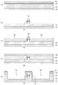
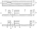
- FIG. 2 is sectional drawing for demonstrating the manufacturing method of the semiconductor device which concerns on Embodiment 1.
- FIG. It is sectional drawing for demonstrating the manufacturing method of the semiconductor device which concerns on Embodiment 1.
- FIG. It is sectional drawing for demonstrating the manufacturing method of the semiconductor device which concerns on Embodiment 1.
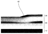
- FIG. It is an SEM photograph which shows the experimental result of etching of the insulating film which concerns on Embodiment 1.
- FIG. It It is a graph which shows the experimental result of the etching rate and the selection ratio which concerns on Embodiment 1.
- FIG. It is an SEM photograph which shows the experimental result of etching of the insulating resin film which concerns on Embodiment 1.
- FIG. It is a figure for demonstrating the inclination angle by etching of the insulating film and the insulating resin film which concerns on Embodiment 1.
- FIG. It is sectional drawing which shows the modification of the semiconductor device which concerns on Embodiment 1.
- FIG. It is sectional drawing which shows another modification of the semiconductor device which concerns on Embodiment 1.
- FIG. It is sectional drawing which shows the semiconductor device which concerns on Embodiment 2.
- Embodiment 1 The configuration of the semiconductor device according to the first embodiment will be described.
- the semiconductor device according to the first embodiment is the semiconductor laser 10 shown in FIG.
- FIG. 1 is a cross-sectional view of the semiconductor laser 10 including a plane perpendicular to the resonator direction.
- the semiconductor laser 10 includes a semiconductor substrate 12.
- the semiconductor substrate 12 is a semi-insulating substrate made of, for example, InP.
- the first conductive clad layer 14 is formed on the semiconductor substrate 12.
- the first conductive clad layer 14 is made of, for example, an n-type InP.
- the portion of the first conductive clad layer 14 connected to the electrode 46 may have a high impurity concentration in order to reduce the electrical resistance.
- a ridge waveguide 26 composed of a first conductive clad layer 14, an active layer 16, and a second conductive clad layer 18 is formed in this order from the bottom.
- the active layer 16 includes, for example, a multiple quantum well structure composed of i-type AlGaInAs.
- the i-type is a semiconductor that has not been intentionally doped.
- the second conductive clad layer 18 is made of, for example, p-type InP.
- the current block layer 20 is embedded on the left and right sides of the ridge waveguide 26.
- the current block layer 20 is made of, for example, Fe-InP (Fe-doped InP).
- a second conductive clad layer 18 is further formed on the ridge waveguide 26 and the current block layer 20.
- a mesa 24 composed of a first conductive clad layer 14, a ridge waveguide 26, a current block layer 20, and a second conductive clad layer 18 is formed.
- the mesa 24 has, for example, a width of 4.0 ⁇ m to 10.0 ⁇ m and a height of 6.0 ⁇ m to 8.0 ⁇ m.
- a groove 54 is formed in the laminate 22 in which the lowermost layer is the first conductive clad layer 14 and the uppermost layer is the second conductive clad layer 18.
- the position of the groove 54 is shown in FIG. 2 (e), which shows the manufacturing process.
- Grooves 54 are dug on both sides of the mesa 24.
- the groove 54 is dug from the upper surface of the second conductive clad layer 18 to the middle of the first conductive clad layer 14.
- the insulating resin film 30 is embedded in the groove 54.
- the insulating resin film 30 is made of a BCB (benzocyclobutene) resin, a polyimide resin, or the like having a low dielectric constant and excellent embedding flatness.
- a first opening 32 is opened on one of the insulating resin films 30 on both sides of the mesa 24.
- the first conductive clad layer is exposed on the bottom surface 36 of the first opening 32.
- the side surface (first side surface 34) of the insulating resin film 30 in contact with the first opening 32 has an inclination in the forward taper direction in which the insulating resin film spreads as it approaches the semiconductor substrate 12.
- the angle ⁇ formed by the first side surface 34 and the lower surface of the insulating resin film 30 is 20 ° or more and 60 ° or less.
- An insulating film 38 is formed on the insulating resin film 30 and the second conductive clad layer 18.
- a second opening 40 is formed in the insulating film 38 so as to be connected to the first opening 32.
- a dashed line is drawn in FIG. 1 to indicate the position of the second opening 40.
- the side surface (second side surface 42) of the insulating film 38 in contact with the second opening 40, that is, the second side surface 42 of the insulating film 38 connected to the first side surface 34 has an inclination in the forward taper direction.
- the insulating film 38 is made of, for example, a silicon oxide film.
- the bottom surface 36 is connected to the first conductive clad layer 14, and an electrode 46 drawn out onto the insulating film 38 is formed along the first side surface 34 and the second side surface 42.
- the electrode 46 has, for example, a laminated structure of Ti / Pt / Au.
- An electrode 48 connected to the second conductive clad layer 18 is formed through a third opening 44 opened in the insulating film 38 above the mesa 24.
- the electrode 48 has, for example, a laminated structure of Ti / Pt / Au.
- the first conductive clad layer 14, the active layer 16, and the second conductive clad layer 18 are sequentially formed on the semiconductor substrate 12. These are formed by epitaxial growth.
- the ridge waveguide 26 is formed.
- a mask 50 having a stripe pattern made of a silicon oxide film is formed.
- dry etching is performed using the mask 50 as an etching mask.
- the first conductive clad layer 14 is etched halfway.
- the current block layers 20 are embedded on the left and right sides of the ridge waveguide 26.
- mask 50 is used for selective epitaxial growth.
- the current block layer 20 is embedded up to the upper surface of the ridge waveguide 26.
- the second conductive clad layer 18 is further grown on the ridge waveguide 26 and the current block layer 20.
- the mask 50 is removed with hydrofluoric acid such as buffered hydrofluoric acid, and then epitaxially grown.
- two grooves 54 are formed to form a mesa 24.
- two grooves 54 are formed by dry etching from the upper surface of the second conductive clad layer 18 to the middle of the first conductive clad layer 14 using the mask 52. As a result, the two grooves 54 form a mesa 24 arranged on both sides.
- the mask 52 is removed from the state of FIG. 2 (e) to form the insulating resin film 30 on the entire surface.
- an adhesion strengthening agent is applied, and then a non-photosensitive BCB resin, which is an insulating resin, is applied thereto by a spin coating method to form a film, and then a thermosetting treatment is performed. Since the insulating resin shrinks and deforms due to the polymerization reaction during the thermosetting treatment, the film thickness is designed in advance by considering the amount of shrinkage.
- the insulating resin it is preferable to use a non-photosensitive BCB resin having a low dielectric constant (for example, a relative permittivity of 2.50 to 2.65) and a small amount of shrinkage during the heat curing treatment.
- the film thickness of the insulating resin film can be obtained, for example, from 1.0 ⁇ m to 26.0 ⁇ m by adjusting the viscosity and the main rotation speed at the time of spin coating.
- thermosetting can be performed by heating in a baking oven, for example, at 250 ° C to 350 ° C, but since it is easily affected by oxidation when the temperature rises, an inactivating gas such as nitrogen or argon is used to keep the oxygen concentration below 100 ppm, for example. It is necessary to perform heat treatment in the atmosphere. Since it is necessary to form an electrode on the mesa 24 later, the thickness of the insulating resin film 30 on the mesa 24 is preferably 1.0 ⁇ m or less.
- the insulating resin film 30 that embeds the two grooves 54 on both sides of the mesa 24 is formed by exposing the top of the mesa 24 by etching back the insulating resin film 30.
- the etchback is a mixed gas of, for example, an oxygen gas and a fluorocarbon gas such as CF 4 , CHF 3 , C 2 F 6 , C 3 F 8 , C 4 F 8. Plasma etching can be applied.
- the insulating film 38 is formed on the insulating resin film 30 and the second conductive clad layer 18.
- the insulating film 38 is formed by, for example, a CVD (Chemical Vapor Deposition) method.
- the photoresist 56 is formed.
- the photoresist 56 is formed, for example, by using a spin coating method or the like.
- a general i-line positive resist or negative resist for stepper exposure can be used.
- an aperture pattern 58 is formed on the photoresist 56 on the insulating resin film 30 embedded in one of the two grooves 54 by using a photolithography method. do.
- a second opening 40 is formed in the insulating film 38 under the opening pattern 58.
- a wet etching treatment containing a chemical solution of hydrofluoric acid is performed.
- the second side surface 42 of the insulating film 38 in contact with the second opening 40 can be inclined in the forward taper direction. This is because the insulating film 38 is isotropically etched.
- the photoresist 56 is removed.
- a stripping solution, oxygen ashing, or the like is used for removing the photoresist 56.
- the removal of the photoresist 56 can be continuously performed in the same chamber as the etching of the insulating resin film 30 performed in the next step, and the step can be simplified.
- the first opening 32 is formed by etching the insulating resin film 30 under the second opening 40 so that the first conductive clad layer 14 is exposed.
- the first side surface 34 of the insulating resin film 30 formed and in contact with the first opening 32 is provided with an inclination in the forward taper direction.
- Etching is performed using the insulating film 38 as a hard mask.
- etching for example, plasma etching using fluorocarbon gas and oxygen gas can be used.
- the mixing ratio of the fluorocarbon gas and the oxygen gas is adjusted to select the ratio (R BCB / R SiO ) of the etching rate (RBCB ) of the insulating resin film 30 and the etching rate (R SiO) of the insulating film 38. (Called the ratio) can be adjusted.
- a mixed gas of C 3 F 8 gas and oxygen gas for example, the mixing ratio of the oxygen gas was adjusted to about 4 to select ratios by 57% by performing the etching of the insulating resin film 30.
- the inclination of the insulating film 38 can be transferred to the insulating resin film 30.
- the insulating film 38 recedes due to etching, and the film thickness becomes thin.
- a third opening 44 is formed in the insulating film 38 on the mesa 24.
- a photolithography method and, for example, reactive ion etching containing a fluorine-based gas are performed again.
- the electrode 46 and the electrode 48 on the mesa are formed to obtain the semiconductor laser 10 shown in FIG.
- an aperture pattern is first formed by a photolithography method using an image reversal resist, a lift-off resist, or the like.
- an electrode having a laminated structure of Ti / Pt / Au is laminated on the entire surface of the wafer by a vapor deposition or sputtering method, and then lifted off.
- an electrode can be formed in the portion where the resist is opened.
- the electrode 46 formed at this time is pulled out onto the insulating film 38 along the first side surface 34 and the second side surface 42 having an inclination in the forward taper direction.
- the second side surface 42 of the insulating film 38 had an inclination in the forward taper direction.
- an insulating resin film 30 made of BCB and an insulating film 38 made of a silicon oxide film were prepared on a semiconductor substrate 12 made of semi-insulating InP.
- a photoresist was formed on the insulating film 38, and an opening pattern was further provided on the photoresist.
- the insulating film 38 was wet-etched with hydrofluoric acid.
- the angle ⁇ formed by the second side surface 42 of the insulating film 38 and the upper surface of the insulating resin film 30 is 20 ° or less.
- the insulating resin film 30 was etched by changing the mixing ratio of oxygen gas, and the first side surface 34 of the insulating resin film 30 was observed. There are three conditions for the mixing ratio of oxygen gas: 57%, 67%, and 83%.
- the state shown in FIG. 5 obtained in the first experiment was subjected to the same plasma etching as in the second experiment.
- the inclination angle ⁇ of the insulating resin film 30 is about 55 °, and fluff and unevenness are not conspicuous on the first side surface 34. Do you get it. This condition is suitable for electrode formation.
- the first side surface 34 became almost vertical as shown in FIG. 7 (c).
- the etching selectivity is not shown in FIG. 6, but is expected to be high.
- the first side surface 34 cannot be uneven, but becomes substantially vertical. That is, the inclination in the forward taper direction cannot be obtained.
- the selection ratio may be around 4, and specifically 3 to 5 is desirable. If the selection ratio is made smaller, there is an advantage that unevenness is less likely to occur. However, there are some disadvantages such as the need to make the insulating film 38 thicker. In consideration of this, the selection ratio is preferably 3 to 5.
- the inclination angle ⁇ of the first side surface of the insulating resin film and the inclination angle ⁇ of the second side surface of the insulating film have a relationship of 3 ⁇ tan ⁇ / tan ⁇ ⁇ 5. This relationship will be described with reference to FIG. 8, which schematically shows the state of etching for forming the first opening 32.
- Both the insulating film 38 and the insulating resin film 30 are scraped by etching.
- the etching rate of the insulating resin film 30 is R BCB
- the etching rate of the insulating film 38 is R SiO .
- the insulating resin film 30 is embedded in the grooves 54 on both sides of the mesa 24, and the electrode 46 connected to the first conductive clad layer 14 is pulled out from the surface side.
- a semiconductor device with suppressed parasitic capacitance can be obtained. Since the insulating resin film generally has a lower dielectric constant than the insulating film such as a semiconductor material, a silicon oxide film or a silicon nitride film, the insulating resin film is formed on both sides of the mesa 24 to form an insulating resin film on the electrode. Parasitic capacitance is suppressed. Further, the parasitic capacitance can be reduced by adopting a surface mount type in which the electrode 46 is pulled out to the surface side.
- the electrode 46 is formed from the bottom surface 36 of the first opening 32 to the insulating film 38.
- the bending angle during pulling out to the top becomes an obtuse angle, and peeling and disconnection of the electrode 46 can be prevented.
- the inclination angles ( ⁇ and ⁇ ) of the first side surface 34 and the second side surface 42 have small variations. Since the second side surface 42 is formed by isotropically wet-etching the insulating film 38, the variation in the inclination angle is small. Since the inclination of the second side surface 42 is transferred to the first side surface 34 according to the etching selectivity of the insulating resin film 30 and the insulating film 38, the variation in the inclination angle is small. Therefore, since the inclination angle is not accidentally steep, it is possible to prevent the electrode 46 from peeling off and disconnecting.
- the insulating film 38 may be removed as shown in FIG. Removal of the insulating film is performed before forming the electrode 46 and the mesa electrode 48. In this figure, the electrode 46 is pulled out on the insulating resin film 30. By removing the insulating film 38, it may be possible to prevent deterioration of the adhesion of the electrodes and the like. Since the insulating film 38 may remain as a reaction product in the upper layer depending on the etching conditions, if it is not removed, it may cause deterioration of adhesion when forming an electrode or the like later. If you remove this, you don't have to worry about it.
- two grooves 54 are formed on both sides of the mesa 24, but there may be three or more grooves 54. That is, two or more grooves 54 are formed in the laminated body 22. And two of the two or more grooves 54 are on both sides of the mesa 24.
- FIG. 10 shows a case where there are three grooves. In this figure, the electrodes 46 are provided in grooves 32 located away from both sides of the mesa 24.
- the first conductive type and the second conductive type are either the p-type or the n-type of the semiconductor, and have different conductive types from each other.
- the first conductive type is p type
- the second conductive type is n type
- the first conductive type is n type
- the second conductive type is p type.
- Embodiment 2 The semiconductor device according to the second embodiment will be described.
- the semiconductor device is a semiconductor laser, whereas in the second embodiment, it is a Mach-Zehnder type phase modulator.
- the difference from the first embodiment will be mainly described.
- the configuration of the semiconductor device according to the second embodiment will be described.
- the semiconductor device according to the second embodiment is the Mach-Zehnder type phase modulator 60 shown in FIG.
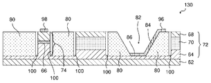
- FIG. 11 is a cross-sectional view taken along the line AA in the top view of the Mach-Zehnder type phase modulator 60 shown in FIG.
- the upper electrode 98, the insulating film 88, and the like are not shown for the sake of explanation.
- the Mach-Zehnder type phase modulator 60 includes a semiconductor substrate 62.
- the first conductive clad layer 64 is formed on the semiconductor substrate 62.
- a mesa 74 composed of a first conductive clad layer 64, an active layer 66, and a second conductive clad layer 68 is formed in this order from the bottom.
- the active layer 66 includes, for example, a multiple quantum well structure composed of i-type AlGaInAs.
- the second conductive clad layer 68 is made of, for example, p-type InP.
- the mesa 74 is also a ridge waveguide having a high mesa structure. That is, the mesa 74 has a ridge waveguide.
- a groove 104 is formed in the laminate 72 in which the lowermost layer is the first conductive clad layer 64 and the uppermost layer is the second conductive clad layer 68.
- the position of the groove 104 is shown in FIG. 14 (b), which shows the manufacturing process.
- the intermediate layer of the laminate 72 between the first conductive clad layer 64 and the second conductive clad layer 68 is an active layer 66 in the mesa 74 and a current block layer 70 in other than the mesa 74.
- a total of three grooves 104 are dug on both sides of the mesa 74 and at a location away from them.
- the groove 104 is dug from the upper surface of the second conductive clad layer 68 to the middle of the first conductive clad layer 64.
- a protective insulating film 100 is formed on the side wall of the laminated body 72.
- the protective insulating film 100 is made of, for example, a silicon oxide film or a silicon nitride film.
- the protective insulating film 100 has the purpose of protecting the mesa 74 from the intrusion of moisture.
- a silicon nitride film is desirable for this purpose.
- the protective insulating film 100 may be omitted.
- An insulating resin film 80 is embedded in the groove 104.
- a first opening 82 is opened in a groove located away from both sides of the mesa 74.
- the first side surface 84 has an inclination in the forward taper direction.
- An insulating film 88 is formed on the insulating resin film 80 and the second conductive clad layer 68.
- a second opening 90 is formed in the insulating film 88.
- a dashed line is drawn in FIG. 11 to indicate the position of the second opening 90.
- the side surface of the insulating film 88 in contact with the second opening 90 (second side surface 92), that is, the second side surface 92 of the insulating film 88 connected to the first side surface 84 has an inclination in the forward taper direction.
- An electrode 96 connected to the first conductive clad layer 64 is formed on the bottom surface 86.
- An electrode 98 on the mesa is formed on the mesa 74.
- the first conductive clad layer 64, the active layer 66, and the second conductive clad layer 68 are formed in this order on the semiconductor substrate 62.
- etching is performed using the mask 102.
- dry etching is performed from the upper surface of the second conductive clad layer 68 to the middle of the first conductive clad layer 64.
- the current block layer 70 is embedded.
- mask 102 is used for selective epitaxial growth.
- the current block layer 70 is embedded up to the upper surface of the second conductive clad layer 68.
- the second conductive clad layer 68 is further grown.
- the mask 102 is removed with hydrofluoric acid such as buffered hydrofluoric acid, and then epitaxially grown. In this step, the laminated body 72 is formed.
- three grooves 104 are formed to form a mesa 74.
- three grooves 104 are formed by dry etching from the upper surface of the second conductive clad layer 68 to the middle of the first conductive clad layer 64 using the mask 103. As a result, two of the three grooves 104 form a mesa 74 arranged on both sides.
- the silicon nitride film is etched back and protected while leaving the silicon nitride film on the side wall of the laminate 72 by dry etching.
- the insulating film 100 is formed.
- dry etching for example, reactive ion etching with a fluorine-based gas such as CF 4 or CHF 3 can be used.
- CF 4 or CHF 3 fluorine-based gas
- the same steps as in the first embodiment are performed to obtain the Mach-Zehnder type phase modulator shown in FIG. Specifically, the same steps as the steps of FIGS. 3 (a) to 4 (d) and the steps of FIGS. 4 (d) to 1 of the first embodiment are performed.
- the first opening 32 is opened in the insulating resin film 30 formed on the side of the mesa 24, but in the second embodiment, as shown in FIG. A first opening 82 is opened in a groove 104 located away from both sides of the mesa 74.
- the second embodiment it is possible to obtain a semiconductor device in which the parasitic capacitance of the electrode is suppressed and the electrode is less likely to be peeled off or broken.
- the insulating film may be removed as shown in FIG. It is the same as the first embodiment that the deterioration of the adhesion of the electrodes and the like can be prevented by removing the insulating film.
- grooves 104 may be formed on both sides of the mesa 74. That is, two or more grooves 104 are formed in the laminated body 72. And two of the two or more grooves 104 are on both sides of the mesa 74.
- FIG. 16 shows a case where there are two grooves. In this figure, the electrode 96 is provided in one of the grooves on both sides of the mesa 74.
Landscapes
- Physics & Mathematics (AREA)
- General Physics & Mathematics (AREA)
- Optics & Photonics (AREA)
- Nonlinear Science (AREA)
- Condensed Matter Physics & Semiconductors (AREA)
- Electromagnetism (AREA)
- Geometry (AREA)
- Semiconductor Lasers (AREA)
- Element Separation (AREA)
Abstract
Description
実施の形態1に係る半導体装置の構成を説明する。実施の形態1に係る半導体装置は図1に示した半導体レーザ10である。図1は半導体レーザ10の共振器方向に垂直な面を含む断面図である。
実施の形態2に係る半導体装置について記載する。実施の形態1では半導体装置が半導体レーザであったのに対し、実施の形態2ではマッハツェンダー型位相変調器である。ここでは主に実施の形態1との違いを記載する。
12,62 半導体基板
14,64 第1導電型クラッド層
16,66 活性層
18,68 第2導電型クラッド層
20,70 電流ブロック層
22,72 積層体
24,74 メサ
26,76 リッジ導波路
28,78 溝
30,80 絶縁性樹脂膜
32,82 第1の開口部
34,84 第1の側面
36,86 底面
38,88 絶縁膜
40,90 第2の開口部
42,92 第2の側面
44,94 第3の開口部
46,96 電極
48,98 メサ上電極
50,102,52,103 マスク2
54,104 溝
56 フォトレジスト
58 開口パターン
60,130,140 マッハツェンダー型位相変調器
100 保護絶縁膜
Claims (9)
- 半導体基板と、
前記半導体基板の上に形成され、最下層が第1導電型クラッド層、最上層が第2導電型クラッド層で構成され、前記第2導電型クラッド層の上面から前記第1導電型クラッド層の途中まで掘られた2つ以上の溝が形成された積層体と、
前記半導体基板に近いほうから順に前記第1導電型クラッド層、活性層、前記第2導電型クラッド層で構成されたリッジ導波路を有し、前記2つ以上の溝のうちの2つが両脇に配置されたメサと、
前記2つ以上の溝に埋め込まれた絶縁性樹脂膜と、を備え、
前記2つ以上の溝のうちの1つに埋め込まれた前記絶縁性樹脂膜には前記第1導電型クラッド層が底面で露出する第1の開口部が形成され、
前記底面で前記第1導電型クラッド層と接続され、前記第1の開口部と接する前記絶縁性樹脂膜の第1の側面に沿って前記絶縁性樹脂膜より上へ引き出された電極が形成され、
前記第1の側面は順テーパ方向の傾斜を持つ半導体装置。 - 前記絶縁性樹脂膜および前記第2導電型クラッド層の上には絶縁膜が形成され、
前記第1の側面に連なる前記絶縁膜の第2の側面は順テーパ方向の傾斜を持ち、
前記電極は前記第2の側面に沿って前記絶縁膜の上へ引き出された請求項1に記載の半導体装置。 - 前記第1の側面と前記絶縁性樹脂膜の下面が成す角度をαとすると、
20°≦α≦60°を満たす請求項1または2に記載の半導体装置。 - 前記第1の側面と前記絶縁性樹脂膜の下面が成す角度をαとし、
前記第2の側面と前記絶縁性樹脂膜の上面が成す角度をβとすると、
3≦tanα/tanβ≦5
を満たす請求項2に記載の半導体装置。 - 前記絶縁性樹脂膜はBCBまたはポリイミド樹脂から成る請求項1~4のいずれか1項に記載の半導体装置。
- 前記リッジ導波路は半導体レーザの共振器である請求項1~5のいずれか1項に記載の半導体装置。
- 前記リッジ導波路はマッハツェンダー型位相変調器の変調導波路である請求項1~5のいずれか1項に記載の半導体装置。
- 半導体基板の上に順に第1導電型クラッド層、活性層および第2導電型クラッド層を形成する工程と、
前記第2導電型クラッド層の上面から前記第1導電型クラッド層の途中までエッチングすることで、2つ以上の溝を形成し、前記半導体基板に近いほうから前記第1導電型クラッド層、前記活性層および前記第2導電型クラッド層で構成されたリッジ導波路を有し、前記2つ以上の溝のうちの2つが両脇に配置されたメサを形成する工程と、
前記2つ以上の溝を埋め込む絶縁性樹脂膜を形成する工程と、
前記絶縁性樹脂膜および前記第2導電型クラッド層の上に絶縁膜を形成する工程と、
前記2つ以上の溝のうちの1つに埋め込まれた前記絶縁性樹脂膜の上の前記絶縁膜をエッチングすることにより第2の開口部を形成し、前記第2の開口部と接する前記絶縁膜の第2の側面に順テーパ方向の傾斜を持たせる工程と、
前記絶縁膜をマスクとし、前記第2の開口部の下の前記絶縁性樹脂膜を前記第1導電型クラッド層が露出するようにエッチングすることにより第1の開口部を形成し、前記第1の開口部と接する前記絶縁性樹脂膜の第1の側面に順テーパ方向の傾斜を持たせる工程と、
前記第1の開口部の底面で前記第1導電型クラッド層と接続され、前記第1の側面に沿って前記絶縁性樹脂膜より上へ引き出された電極を形成する工程と、を備えた半導体装置の製造方法。 - 前記第1の側面に順テーパ方向の傾斜を持たせる工程と、前記電極を形成する工程の間に、前記絶縁膜を除去する工程を備える請求項8に記載の半導体装置の製造方法。
Priority Applications (4)
| Application Number | Priority Date | Filing Date | Title |
|---|---|---|---|
| CN202080089383.8A CN115210976B (zh) | 2020-03-16 | 2020-03-16 | 半导体装置以及半导体装置的制造方法 |
| JP2020544303A JP6809655B1 (ja) | 2020-03-16 | 2020-03-16 | 半導体装置および半導体装置の製造方法 |
| PCT/JP2020/011431 WO2021186497A1 (ja) | 2020-03-16 | 2020-03-16 | 半導体装置および半導体装置の製造方法 |
| US17/756,249 US12348006B2 (en) | 2020-03-16 | 2020-03-16 | Semiconductor device and method for manufacturing semiconductor device |
Applications Claiming Priority (1)
| Application Number | Priority Date | Filing Date | Title |
|---|---|---|---|
| PCT/JP2020/011431 WO2021186497A1 (ja) | 2020-03-16 | 2020-03-16 | 半導体装置および半導体装置の製造方法 |
Publications (1)
| Publication Number | Publication Date |
|---|---|
| WO2021186497A1 true WO2021186497A1 (ja) | 2021-09-23 |
Family
ID=73992864
Family Applications (1)
| Application Number | Title | Priority Date | Filing Date |
|---|---|---|---|
| PCT/JP2020/011431 Ceased WO2021186497A1 (ja) | 2020-03-16 | 2020-03-16 | 半導体装置および半導体装置の製造方法 |
Country Status (4)
| Country | Link |
|---|---|
| US (1) | US12348006B2 (ja) |
| JP (1) | JP6809655B1 (ja) |
| CN (1) | CN115210976B (ja) |
| WO (1) | WO2021186497A1 (ja) |
Citations (4)
| Publication number | Priority date | Publication date | Assignee | Title |
|---|---|---|---|---|
| JPH07135369A (ja) * | 1993-11-11 | 1995-05-23 | Nippon Telegr & Teleph Corp <Ntt> | 半導体レーザおよびその製造方法 |
| JP2012209489A (ja) * | 2011-03-30 | 2012-10-25 | Fujitsu Ltd | 光半導体素子及びその製造方法 |
| JP2014038322A (ja) * | 2012-07-19 | 2014-02-27 | Sumitomo Electric Ind Ltd | 光半導体素子の製造方法 |
| JP2016046393A (ja) * | 2014-08-22 | 2016-04-04 | 住友電工デバイス・イノベーション株式会社 | 半導体レーザ素子 |
Family Cites Families (14)
| Publication number | Priority date | Publication date | Assignee | Title |
|---|---|---|---|---|
| US4487652A (en) | 1984-03-30 | 1984-12-11 | Motorola, Inc. | Slope etch of polyimide |
| JPS6159735A (ja) | 1984-08-30 | 1986-03-27 | Matsushita Electric Ind Co Ltd | 結晶エツチング方法 |
| US5940732A (en) | 1995-11-27 | 1999-08-17 | Semiconductor Energy Laboratory Co., | Method of fabricating semiconductor device |
| JP2000208871A (ja) * | 1999-01-19 | 2000-07-28 | Oki Electric Ind Co Ltd | 導波路型光素子,導波路型光素子の製造方法,光モジュ―ル,及び光モジュ―ルの製造方法 |
| KR100361593B1 (ko) * | 2000-11-23 | 2002-11-22 | 주식회사일진 | 볼록 요철을 갖는 광학집적회로 소자, 그 제조방법, 그광학집적 회로 소자를 이용하여 제조한 광통신용 송수신장치의 모듈 |
| US6687268B2 (en) * | 2001-03-26 | 2004-02-03 | Seiko Epson Corporation | Surface emitting laser and photodiode, manufacturing method therefor, and optoelectric integrated circuit using the surface emitting laser and the photodiode |
| JP2004342719A (ja) * | 2003-05-14 | 2004-12-02 | Toshiba Corp | 半導体レーザ装置及びその製造方法 |
| JP5061951B2 (ja) * | 2008-02-26 | 2012-10-31 | 富士通株式会社 | 光半導体装置の製造方法 |
| JP5167052B2 (ja) | 2008-09-30 | 2013-03-21 | パナソニック株式会社 | ドライエッチング方法 |
| JP5292443B2 (ja) * | 2011-07-25 | 2013-09-18 | 日本オクラロ株式会社 | 光半導体素子の製造方法 |
| CN203218310U (zh) * | 2013-04-01 | 2013-09-25 | 天津三安光电有限公司 | 发光器件、照明装置及显示系统 |
| JP2016184680A (ja) | 2015-03-26 | 2016-10-20 | 住友電気工業株式会社 | 半導体光素子 |
| TW201810703A (zh) | 2016-06-07 | 2018-03-16 | 村田製作所股份有限公司 | 半導體裝置及其製造方法 |
| CN110914745A (zh) * | 2017-08-01 | 2020-03-24 | 三菱电机株式会社 | 光半导体元件的制造方法及光半导体元件 |
-
2020
- 2020-03-16 WO PCT/JP2020/011431 patent/WO2021186497A1/ja not_active Ceased
- 2020-03-16 JP JP2020544303A patent/JP6809655B1/ja active Active
- 2020-03-16 CN CN202080089383.8A patent/CN115210976B/zh active Active
- 2020-03-16 US US17/756,249 patent/US12348006B2/en active Active
Patent Citations (4)
| Publication number | Priority date | Publication date | Assignee | Title |
|---|---|---|---|---|
| JPH07135369A (ja) * | 1993-11-11 | 1995-05-23 | Nippon Telegr & Teleph Corp <Ntt> | 半導体レーザおよびその製造方法 |
| JP2012209489A (ja) * | 2011-03-30 | 2012-10-25 | Fujitsu Ltd | 光半導体素子及びその製造方法 |
| JP2014038322A (ja) * | 2012-07-19 | 2014-02-27 | Sumitomo Electric Ind Ltd | 光半導体素子の製造方法 |
| JP2016046393A (ja) * | 2014-08-22 | 2016-04-04 | 住友電工デバイス・イノベーション株式会社 | 半導体レーザ素子 |
Also Published As
| Publication number | Publication date |
|---|---|
| US20220416511A1 (en) | 2022-12-29 |
| US12348006B2 (en) | 2025-07-01 |
| JP6809655B1 (ja) | 2021-01-06 |
| CN115210976B (zh) | 2025-02-25 |
| CN115210976A (zh) | 2022-10-18 |
| JPWO2021186497A1 (ja) | 2021-09-23 |
Similar Documents
| Publication | Publication Date | Title |
|---|---|---|
| JP2823476B2 (ja) | 半導体レーザおよびその製造方法 | |
| CN101950924B (zh) | 半导体光学元件的制造方法 | |
| CN1224150C (zh) | 脊形波导型半导体激光装置 | |
| JP6206247B2 (ja) | 半導体装置の製造方法 | |
| JP2014038322A (ja) | 光半導体素子の製造方法 | |
| JPS63107119A (ja) | ステップ絶縁層を有する集積回路の製造方法 | |
| US20120058582A1 (en) | Method for etching insulating film and method for manufacturing semiconductor optical device | |
| JP6809655B1 (ja) | 半導体装置および半導体装置の製造方法 | |
| CN101877456A (zh) | 半导体发光元件的制造方法及半导体发光元件 | |
| JP3621752B2 (ja) | Iii−v族半導体ゲート構造の製造方法 | |
| JP5531610B2 (ja) | 半導体レーザ素子の製造方法 | |
| JP2013149746A (ja) | 光集積素子の製造方法 | |
| US7781245B2 (en) | Method to fabricate semiconductor optical device | |
| JPWO2019026943A1 (ja) | 光半導体素子の製造方法および光半導体素子 | |
| JP2013250527A (ja) | 半導体マッハツェンダ変調器および半導体マッハツェンダ変調器の製造方法 | |
| JP2013044803A (ja) | 光半導体素子の製造方法 | |
| WO1991013480A1 (fr) | Dispositif a semi-conducteurs optique du type a enfouissement mesa et sa fabrication | |
| JP2013077797A (ja) | 半導体レーザおよびその製造方法 | |
| JP7806265B2 (ja) | 光電子デバイスを処理する方法及び光電子デバイス | |
| CN110176398B (zh) | 等离子体刻蚀方法及垂直腔面发射激光器制备方法 | |
| JP4609830B2 (ja) | 半導体装置の製造方法 | |
| JP5028811B2 (ja) | 化合物半導体光デバイスを作製する方法 | |
| US11500157B1 (en) | Silicon Selective Epitaxial Growth (SEG) applied to a Silicon on Insulator (SOI) wafer to provide a region of customized thickness | |
| JP2018101752A (ja) | 半導体光素子およびその製造方法 | |
| JPH04369886A (ja) | 半導体レーザの製造方法 |
Legal Events
| Date | Code | Title | Description |
|---|---|---|---|
| ENP | Entry into the national phase |
Ref document number: 2020544303 Country of ref document: JP Kind code of ref document: A |
|
| 121 | Ep: the epo has been informed by wipo that ep was designated in this application |
Ref document number: 20925805 Country of ref document: EP Kind code of ref document: A1 |
|
| NENP | Non-entry into the national phase |
Ref country code: DE |
|
| 122 | Ep: pct application non-entry in european phase |
Ref document number: 20925805 Country of ref document: EP Kind code of ref document: A1 |
|
| WWG | Wipo information: grant in national office |
Ref document number: 202080089383.8 Country of ref document: CN |
|
| WWG | Wipo information: grant in national office |
Ref document number: 17756249 Country of ref document: US |