WO2021182413A1 - 発光装置 - Google Patents
発光装置 Download PDFInfo
- Publication number
- WO2021182413A1 WO2021182413A1 PCT/JP2021/009056 JP2021009056W WO2021182413A1 WO 2021182413 A1 WO2021182413 A1 WO 2021182413A1 JP 2021009056 W JP2021009056 W JP 2021009056W WO 2021182413 A1 WO2021182413 A1 WO 2021182413A1
- Authority
- WO
- WIPO (PCT)
- Prior art keywords
- light emitting
- emitting element
- emitting device
- emitting elements
- light
- Prior art date
- Legal status (The legal status is an assumption and is not a legal conclusion. Google has not performed a legal analysis and makes no representation as to the accuracy of the status listed.)
- Ceased
Links
Images









Classifications
-
- H—ELECTRICITY
- H10—SEMICONDUCTOR DEVICES; ELECTRIC SOLID-STATE DEVICES NOT OTHERWISE PROVIDED FOR
- H10W—GENERIC PACKAGES, INTERCONNECTIONS, CONNECTORS OR OTHER CONSTRUCTIONAL DETAILS OF DEVICES COVERED BY CLASS H10
- H10W90/00—Package configurations
-
- H—ELECTRICITY
- H10—SEMICONDUCTOR DEVICES; ELECTRIC SOLID-STATE DEVICES NOT OTHERWISE PROVIDED FOR
- H10H—INORGANIC LIGHT-EMITTING SEMICONDUCTOR DEVICES HAVING POTENTIAL BARRIERS
- H10H20/00—Individual inorganic light-emitting semiconductor devices having potential barriers, e.g. light-emitting diodes [LED]
- H10H20/80—Constructional details
- H10H20/85—Packages
- H10H20/851—Wavelength conversion means
- H10H20/8514—Wavelength conversion means characterised by their shape, e.g. plate or foil
-
- H—ELECTRICITY
- H10—SEMICONDUCTOR DEVICES; ELECTRIC SOLID-STATE DEVICES NOT OTHERWISE PROVIDED FOR
- H10H—INORGANIC LIGHT-EMITTING SEMICONDUCTOR DEVICES HAVING POTENTIAL BARRIERS
- H10H20/00—Individual inorganic light-emitting semiconductor devices having potential barriers, e.g. light-emitting diodes [LED]
- H10H20/80—Constructional details
- H10H20/85—Packages
- H10H20/851—Wavelength conversion means
- H10H20/8516—Wavelength conversion means having a non-uniform spatial arrangement or non-uniform concentration, e.g. patterned wavelength conversion layer or wavelength conversion layer with a concentration gradient
-
- H—ELECTRICITY
- H10—SEMICONDUCTOR DEVICES; ELECTRIC SOLID-STATE DEVICES NOT OTHERWISE PROVIDED FOR
- H10H—INORGANIC LIGHT-EMITTING SEMICONDUCTOR DEVICES HAVING POTENTIAL BARRIERS
- H10H20/00—Individual inorganic light-emitting semiconductor devices having potential barriers, e.g. light-emitting diodes [LED]
- H10H20/80—Constructional details
- H10H20/85—Packages
- H10H20/852—Encapsulations
- H10H20/854—Encapsulations characterised by their material, e.g. epoxy or silicone resins
-
- H—ELECTRICITY
- H10—SEMICONDUCTOR DEVICES; ELECTRIC SOLID-STATE DEVICES NOT OTHERWISE PROVIDED FOR
- H10H—INORGANIC LIGHT-EMITTING SEMICONDUCTOR DEVICES HAVING POTENTIAL BARRIERS
- H10H20/00—Individual inorganic light-emitting semiconductor devices having potential barriers, e.g. light-emitting diodes [LED]
- H10H20/80—Constructional details
- H10H20/85—Packages
- H10H20/857—Interconnections, e.g. lead-frames, bond wires or solder balls
-
- H—ELECTRICITY
- H10—SEMICONDUCTOR DEVICES; ELECTRIC SOLID-STATE DEVICES NOT OTHERWISE PROVIDED FOR
- H10H—INORGANIC LIGHT-EMITTING SEMICONDUCTOR DEVICES HAVING POTENTIAL BARRIERS
- H10H20/00—Individual inorganic light-emitting semiconductor devices having potential barriers, e.g. light-emitting diodes [LED]
- H10H20/01—Manufacture or treatment
- H10H20/036—Manufacture or treatment of packages
- H10H20/0361—Manufacture or treatment of packages of wavelength conversion means
-
- H—ELECTRICITY
- H10—SEMICONDUCTOR DEVICES; ELECTRIC SOLID-STATE DEVICES NOT OTHERWISE PROVIDED FOR
- H10H—INORGANIC LIGHT-EMITTING SEMICONDUCTOR DEVICES HAVING POTENTIAL BARRIERS
- H10H20/00—Individual inorganic light-emitting semiconductor devices having potential barriers, e.g. light-emitting diodes [LED]
- H10H20/01—Manufacture or treatment
- H10H20/036—Manufacture or treatment of packages
- H10H20/0362—Manufacture or treatment of packages of encapsulations
-
- H—ELECTRICITY
- H10—SEMICONDUCTOR DEVICES; ELECTRIC SOLID-STATE DEVICES NOT OTHERWISE PROVIDED FOR
- H10H—INORGANIC LIGHT-EMITTING SEMICONDUCTOR DEVICES HAVING POTENTIAL BARRIERS
- H10H20/00—Individual inorganic light-emitting semiconductor devices having potential barriers, e.g. light-emitting diodes [LED]
- H10H20/80—Constructional details
- H10H20/84—Coatings, e.g. passivation layers or antireflective coatings
-
- H—ELECTRICITY
- H10—SEMICONDUCTOR DEVICES; ELECTRIC SOLID-STATE DEVICES NOT OTHERWISE PROVIDED FOR
- H10H—INORGANIC LIGHT-EMITTING SEMICONDUCTOR DEVICES HAVING POTENTIAL BARRIERS
- H10H20/00—Individual inorganic light-emitting semiconductor devices having potential barriers, e.g. light-emitting diodes [LED]
- H10H20/80—Constructional details
- H10H20/85—Packages
- H10H20/851—Wavelength conversion means
- H10H20/8511—Wavelength conversion means characterised by their material, e.g. binder
- H10H20/8512—Wavelength conversion materials
-
- H—ELECTRICITY
- H10—SEMICONDUCTOR DEVICES; ELECTRIC SOLID-STATE DEVICES NOT OTHERWISE PROVIDED FOR
- H10H—INORGANIC LIGHT-EMITTING SEMICONDUCTOR DEVICES HAVING POTENTIAL BARRIERS
- H10H20/00—Individual inorganic light-emitting semiconductor devices having potential barriers, e.g. light-emitting diodes [LED]
- H10H20/80—Constructional details
- H10H20/85—Packages
- H10H20/851—Wavelength conversion means
- H10H20/8511—Wavelength conversion means characterised by their material, e.g. binder
- H10H20/8512—Wavelength conversion materials
- H10H20/8513—Wavelength conversion materials having two or more wavelength conversion materials
Definitions
- This disclosure relates to a light emitting device.
- a light emitting device capable of emitting light having a high color mixing property and a different color temperature is known.
- Japanese Patent Application Laid-Open No. 2014-45089 describes a light emitting device in which a plurality of LED dies are grouped in a striped or mosaic pattern to form an LED group, and each of the LED groups is coated with at least two types of phosphor layers. Is described.
- the light emitting device described in JP-A-2014-45089 has high color mixing property of light having a plurality of colors by forming a plurality of LED groups coated with phosphor layers having different color temperatures of the emitted light. Can be emitted.
- the phosphor layer covering the LED group is arranged so as to cover all four side surfaces in addition to the upper surface of the LED die included in the LED group. Therefore, the amount of the phosphor arranged around the LED die increases.
- the amount of the phosphor arranged around the LED die is reduced.
- the amount of the phosphor arranged on the upper surface of the LED die increases, and the luminous efficiency of the light emitting device may decrease.
- An object of the present disclosure is to provide a light emitting device in which the amount of phosphor used is suppressed and the luminous efficiency is less likely to decrease.
- the light emitting device is a substrate and a plurality of light emitting elements each having a rectangular planar shape and mounted on the substrate, and each of the plurality of light emitting elements is provided.
- At least one side surface is a plurality of light emitting elements arranged so as to face the side surfaces of the other light emitting elements, and at least a part of the upper surface of at least two light emitting elements of the plurality of light emitting elements and at least a part of the facing side surfaces.
- a first wavelength conversion member arranged so as to cover at least a part of the non-opposing side surfaces of at least two light emitting elements, and a sealing material for sealing the plurality of light emitting elements and the first wavelength conversion member. And have.
- the first wavelength conversion member is arranged so as not to cover the vicinity of the angle most distant from the opposite side surface on the upper surface of at least two light emitting elements.
- the first wavelength conversion member is arranged so as to cover the vicinity of the side adjacent to the opposite side surface on the non-opposing side surface of at least two light emitting elements.
- the first wavelength conversion member is arranged so as not to cover the vicinity of the side arranged on the outside on the opposite side surfaces of at least two light emitting elements.
- the plurality of light emitting elements are a plurality of first light emitting element trains in which light emitting elements arranged so that the first wavelength conversion member covers the upper surface and the opposite side surfaces are connected in series. It is preferable that the first wavelength conversion member includes a plurality of second light emitting element trains in which light emitting elements which are not arranged so as to cover the upper surface and the opposite side surfaces are connected in series.
- each of the plurality of first light emitting element rows includes a first light emitting element group having a plurality of light emitting elements arranged in each of the plurality of first mounting areas having the same area. It is preferable to include it.
- each of the plurality of first light emitting element groups includes four light emitting elements arranged in 2 rows and 2 columns.
- each of the plurality of second light emitting element rows includes a second light emitting element group having a plurality of light emitting elements arranged in each of the plurality of second mounting areas having the same area. It is preferable to include it.
- the second light emitting element row has a light emitting element that is not arranged in any of the second mounting areas.
- the light emitting element that is not arranged in any of the second mounting areas is arranged in the area between any of the first mounting areas and the outer edge of the mounting area in which the light emitting element is mounted. Is preferable.
- the sealing material contains a second wavelength conversion member, and the first light emitting element included in each of the plurality of first light emitting element trains emits light.
- the color temperature of the light is preferably different from the color temperature of the second light emitted when the light emitting element included in each of the plurality of second light emitting element rows emits light.
- the plurality of first light emitting element groups and the plurality of second light emitting element groups are arranged in parallel in the same direction.
- the plurality of first light emitting element groups and the plurality of second light emitting element groups are arranged in a straight line.
- the plurality of first light emitting element groups and the plurality of second light emitting element groups are arranged in a zigzag pattern.
- a pair of first electrode pairs that supply power to a plurality of first light emitting element rows, and a plurality of first light emitting element rows and a pair of first electrode pairs are electrically connected.
- the first wiring further includes a second wiring pattern that electrically connects the light emitting element row and the pair of second electrode pairs, and a second overvoltage prevention element that is connected in parallel to the plurality of second light emitting element rows. It is preferable that either the pattern or the second wiring pattern has a plurality of wiring patterns electrically connected via a bonding wire.
- one end of the bonding wire is connected to a wiring pattern connected to a light emitting element included in any one of a plurality of first light emitting element rows and a plurality of second light emitting element rows. Is preferable.
- one end of the bonding wire is connected to a wiring pattern connected to either one of the first overvoltage prevention element and the second overvoltage prevention element.
- the light emitting device is formed of a material different from the sealing material, and further has a substrate, a plurality of light emitting elements, a first wavelength conversion member, and a transparent layer arranged between the sealing material. Is preferable.
- the bonding wire is formed of a plurality of conductive wires connected in parallel.
- the light emitting device can suppress a decrease in luminous efficiency while suppressing the amount of phosphor used.
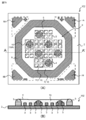
- FIG. 1 It is a top view of the light emitting device which concerns on 1st Embodiment.
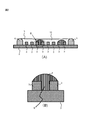
- A is a cross-sectional view taken along the line AA'of the light emitting device shown in FIG. 1, and (B) is a partially enlarged view of the cross-sectional view shown in (A).
- (A) is a plan view of the light emitting device according to the fourth modification, and (b) is a cross-sectional view taken along the line AA'of the light emitting device shown in (a).
- (A) is a plan view of the light emitting device according to the fifth modification, and (b) is a cross-sectional view taken along the line AA'of the light emitting device shown in (a).
- (A) is a plan view of the light emitting device according to the sixth modification, and (b) is a cross-sectional view taken along the line AA'of the light emitting device shown in (a).
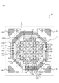
- FIG. 1 is a plan view of the light emitting device according to the first embodiment
- FIG. 2A is a cross-sectional view taken along the line AA'of the light emitting device shown in FIG. 1
- FIG. 2B is FIG. It is a partially enlarged view which is shown by the arrow B in (A).
- the bonding wire is omitted in FIGS. 1, 2 (A) and 2 (B).
- the light emitting device 1 includes a substrate 2, a plurality of light emitting elements 3, a first phosphor 4, a sealing material 5, and a dam material 6.
- the substrate 2 is a flat substrate formed of an insulating resin such as glass epoxy.
- the substrate 2 has a square planar shape, and the first electrode pairs 7A and 7B and the second electrode pairs 8A and 8B are arranged.
- the substrate 2 may have another planar shape such as a rectangle instead of a square, and includes a mounting substrate formed of a member having high thermal conductivity such as aluminum and an insulating circuit board on which a wiring pattern is formed. May be formed with.
- the first electrode pairs 7A and 7B and the second electrode pairs 8A and 8B are formed of a conductive member such as gold plating on the upper surface of the substrate 2, and a plurality of light emitting elements 3 receive power supplied from an external power source (not shown). It is an anode terminal and a cathode terminal to be supplied to each of the above.
- a mounting region 9 having a substantially regular octagonal planar shape and on which a plurality of light emitting elements 3 are mounted is formed in the central portion of the substrate 2.
- the planar shape of the mounting region 9 is not limited to a substantially regular octagon, and may be other shapes such as a circular shape, an annular shape, and a polygonal shape.
- the light emitting element 3 is an LED (Light Emitting Diode) die that emits blue light, and 48 light emitting elements 3 are arranged in the mounting area 9.
- Each of the light emitting elements 3 has a rectangular planar shape, and the light emitting elements 3 are mounted in the mounting region 9 of the substrate 2 so that the two side surfaces face the side surfaces of the other light emitting elements 3.
- the pair of light emitting elements 3 are arranged so that the opposite side surfaces are arranged in parallel and face each other over the entire surface.
- the first phosphor 4 is, for example, YAG (Yttrium Aluminum Garnet), which is a first wavelength conversion member that absorbs blue light emitted by a light emitting element 3 and emits light such as red, green, and yellow, and is made of silicone. It is contained in a transparent resin such as a resin and arranged.
- the four light emitting elements 3 covered with the first phosphor 4 and arranged in an array of 2 rows and 2 columns have 6 first light emitting elements arranged in each of the 6 first mounting areas 10A having the same area.
- the element group 10 is formed.
- the first light emitted from the light emitting element 3 included in the first light emitting element group 10 and passing through both the first phosphor 4 and the sealing material 5 is a warm white light having a color temperature of, for example, 2700 K or 3000 K. Is.
- the first phosphor 4 is arranged on the upper surface of each of the four light emitting elements 3 included in the first light emitting element group 10, and the opposite side surfaces of the adjacent light emitting elements 3 and the space S formed by the substrate 2. Is arranged to fill. Since the first phosphor 4 is filled between the four light emitting elements 3 arranged in an array of 2 rows and 2 columns, the space S in which the four light emitting elements 3 included in the first light emitting element group 10 are filled. Has a cross-shaped planar shape.
- the region that can be arranged in the vicinity of the light emitting element 3 increases as compared with the case where the first phosphor 4 is arranged only on the upper surface of the light emitting element 3. ..
- the region where the first phosphor 4 can be arranged increases in the vicinity of the light emitting element 3 as compared with the case where the first phosphor 4 is arranged only on the upper surface of the light emitting element 3, so that the first phosphor 4 is arranged on the upper surface of the light emitting element 3. 1
- the amount of phosphor 4 can be reduced.
- the luminous device 1 can increase the luminous efficiency by filling the space S with the first phosphor 4 and reducing the amount of the first phosphor 4 arranged on the upper surface of the light emitting element 3.
- the four light emitting elements 3 arranged in a two-row, two-column array in which the first phosphor 4 is not arranged on the upper surface are the six seconds arranged in each of the six second mounting areas 11A having the same area.
- the light emitting element group 11 is formed.
- the area of the second mounting area 11A in which the second light emitting element group 11 is arranged is the same as the area of the first mounting area 10A in which the first light emitting element group 10 is arranged.
- the sealing material 5 is a transparent resin such as a silicone resin that fills the space on the mounting region 9, and seals a plurality of light emitting elements 3 and the first phosphor 4. Further, the sealing material 5 contains the second phosphor 13.
- the second phosphor 13 is, for example, YAG, which is a second wavelength conversion member that absorbs blue light emitted by the light emitting element 3 and emits light such as red, green, and yellow. The color of the light emitted by the second phosphor 13 is different from the color of the light emitted by the first phosphor 4.
- the second light emitted from the light emitting element 3 included in the second light emitting element group 11 and passing through the sealing material 5 is cold white light having a color temperature of, for example, 5000 K.
- the dam material 6 is a frame material formed of an opaque silicone resin mixed with white particles, which prevents the sealing material 5 filled in the mounting region 9 from flowing out and the light emitting element 3 and the first phosphor. It reflects the light emitted from the 4th and the 2nd phosphor 13.
- Each of the first light emitting element group 10 and the plurality of second light emitting element groups 11 is linearly arranged parallel to the extending direction of the broken line 12 in FIG.
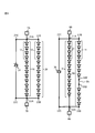
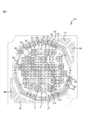
- FIG. 3 is a plan view of the light emitting device 1 in which the sealing material 5 and the dam material 6 are omitted, and FIG. 4 is a circuit diagram of the light emitting device 1.
- the light emitting device 1 further includes a first wiring pattern 21 to 23, a first overvoltage prevention element 24, a second wiring pattern 31 to 35, and a second overvoltage prevention element 36.
- the four light emitting elements 3 included in each of the first light emitting element group 10 and the second light emitting element group 11 are connected in series via a bonding wire.
- the three first light emitting element groups 10 are connected in series via a bonding wire to form a pair of first light emitting element rows 25 and 26 connected in parallel.
- the three second light emitting element groups 11 are connected in series via a bonding wire to form a pair of second light emitting element rows 37 and 38 connected in parallel.
- the first light emitting element rows 25 and 26 are connected to the first electrode pairs 7A and 7B via the first wiring patterns 21 to 23, and are also connected in parallel to the first overvoltage prevention element 24.
- the second light emitting element rows 37 and 38 are connected to the second electrode pairs 8A and 8B via the second wiring patterns 31 to 35, and are connected in parallel to the second overvoltage prevention element 36.
- the first wiring pattern 21 is a wiring pattern integrally formed with the first electrode pair 7A, and the first wiring pattern 21 has contacts 21A, 21B and 21C.
- the first wiring pattern 22 is a wiring pattern integrally formed with the cathode electrode 7B, and has contacts 22A and 22C.
- the first wiring pattern 23 is a wiring pattern integrally formed with the cathode electrode 7B and has a contact 23B.
- the first light emitting element row 25 is connected between the contact 21A of the first wiring pattern 21 and the contact 22A of the first wiring pattern 22 via a bonding wire.
- the first light emitting element row 26 is connected between the contact 21B of the first wiring pattern 21 and the contact 23B of the first wiring pattern 23 via a bonding wire.
- the first overvoltage prevention element 24 is a Zener diode, and when an overvoltage is applied between the first electrode pairs 7A and 7B, a breakdown current flows through the light emitting element 3 included in the first light emitting element rows 25 and 26. Prevents overvoltage from being applied.
- the second wiring pattern 31 is a wiring pattern integrally formed with the second electrode pair 8A, is arranged outside the first wiring pattern 21, and has contacts 31A, 31B, and 31C.
- the second wiring pattern 32 is a wiring pattern formed so as to be separated from other wiring patterns, is arranged inside the first wiring pattern 22, the second wiring patterns 34, and 35, and has contacts 32A and 32A'.
- the second wiring pattern 33 is a wiring pattern integrally formed with the cathode electrode 8B, and has contacts 33A, 33B, and 33C.
- the second wiring pattern 34 is a wiring pattern formed so as to be separated from other wiring patterns, is arranged outside the second wiring pattern 32, and has contacts 34B and 34B'.
- the second wiring pattern 35 is a wiring pattern formed so as to be separated from other wiring patterns, is arranged outside the second wiring pattern 32, and has contacts 35B and 35B'.
- the second light emitting element row 37 is connected between the contact 31A of the second wiring pattern 31 and the contact 33A of the second wiring pattern 33 via a bonding wire and a second wiring pattern 32.
- the second light emitting element row 38 is connected between the contact 31B of the second wiring pattern 31 and the contact 33B of the second wiring pattern 33 via a bonding wire, a second wiring pattern 34, and a second wiring pattern 35.
- the second wiring pattern 34 and the second wiring pattern 35 are connected by a jumper Bx which is a bonding wire.
- the second overvoltage prevention element 36 is a Zener diode, and when an overvoltage is applied between the second electrode pairs 8A and 8B, a breakdown current flows through the light emitting element 3 included in the second light emitting element rows 37 and 38. Prevents overvoltage from being applied.
- the light emitting element 3 included in the first light emitting element rows 25 and 26 emits light to emit light to the light emitting device. 1 emits a first light which is a warm white light.
- the light emitting element 3 included in the second light emitting element rows 37 and 38 emits light.
- the light emitting device 1 emits a second light which is cold white light.
- the color temperature of the mixed light of the first light and the second light is a color temperature intermediate between the color temperature of the first light and the color temperature of the second light.
- FIGS. 5A and 5B are views showing a manufacturing method of the light emitting device 1
- FIG. 5A shows a first step
- FIG. 5B shows a second step
- FIG. 5C shows a third step
- FIG. 5 (D) shows the fourth step.
- the figures shown in FIGS. 5 (A) to 5 (D) are cross sections corresponding to the cross sections along the AA'line shown in FIG.
- a plurality of light emitting elements 3 are arranged in the mounting region 9 of the substrate 2, and wire bonding is performed between the plurality of light emitting elements and between the second wiring pattern 34 and the second wiring pattern 35.
- the dam material 6 is arranged so as to surround the mounting area 9 along the outer edge of the mounting area 9.
- the first phosphor 4 is placed between the opposite side surfaces of the four light emitting elements 3 arranged in two rows and two columns included in the first light emitting element group 10 and on the upper surface of the four light emitting elements 3. Place the resin containing.
- the resin containing the first phosphor 4 is held by surface tension at the opposite side surface and upper surface end portions of the four light emitting elements 3.
- the fourth step the resin that is the base material of the sealing material 5 is filled and solidified inside the dam material 6, and the manufacturing process of the light emitting device 1 is completed.
- the first light emitting element group 10 that emits the first light and the second light emitting element group 11 that emits the first light are alternately arranged, so that light having good color mixing property is emitted. can do.
- the first phosphor 4 is arranged between the upper surface of the light emitting element 3 and the opposite side surfaces of the light emitting element 3, the first phosphor arranged on the upper surface of the light emitting element 3.
- the luminous efficiency can be increased.
- the first light emitting element group 10 since the first light emitting element group 10 and the plurality of second light emitting element groups 11 are arranged in a straight line in parallel in the same direction, the light emitting element 3 of the light emitting element 3 does not cross the bonding wires. Can connect between.
- the bonding wires connecting the light emitting elements 3 mounted in the mounting region 9 do not intersect with each other. Can be placed.
- the bonding wires connecting the light emitting elements 3 mounted in the mounting region 9 are arranged so as not to intersect each other, thereby preventing short circuits of the bonding wires.
- the jumper Bx is arranged at a position connecting the second light emitting element group 11 included in the second light emitting element row 38, so that only the current flowing through the second light emitting element row 38 is arranged in the jumper Bx. Flows, and the current flowing through the second light emitting element row 37 does not flow. Since only the current flowing in the second light emitting element row 38 flows through the jumper Bx having large resistance values of the first wiring patterns 21 to 23 and the second wiring patterns 31 to 35, the increase in power consumption due to the current flowing through the jumper Bx is suppressed. be able to.
- FIG. 6 is a plan view of the light emitting device according to the second embodiment. In FIG. 6, the bonding wire is omitted.
- the light emitting device 40 differs from the light emitting device 1 in the arrangement of the light emitting elements 3 included in the second light emitting element group 11.
- the components and functions of the light emitting device 40 other than the arrangement of the light emitting elements 3 included in the second light emitting element group 11 are the same as the components and functions of the light emitting device 1 having the same reference numerals. A detailed description will be omitted.
- one void 41 in which the light emitting element 3 is not arranged is formed in each of the second mounting areas 11A in which the light emitting element 3 included in the second light emitting element group 11 is arranged.
- the light emitting element 3A corresponding to the light emitting element 3 arranged at the position corresponding to the void 41 in the light emitting device 1 is arranged in the region between the first mounting area 10A and the outer edge of the mounting region 9.
- FIG. 7 is a plan view of the light emitting device 40 in which the sealing material 5 and the dam material 6 are omitted.
- the connection relationship of the light emitting elements 3 included in the second light emitting element rows 37 and 38 emits light. It is different from the connection relationship in the device 1.
- the light emitting device 40 arranges the light emitting element 3A in the region between the first mounting area 10A and the outer edge of the mounting region 9, so that the arrangement shape of the light emitting element 3 included in the second light emitting element group 11 can be changed to the mounting region. It can approach the shape of 9. By making the arrangement shape of the light emitting element 3 close to the shape of the mounting region 9, the light emitting device 40 can emit light having less color unevenness and light unevenness and improved uniformity.
- FIG. 8 is a plan view of the light emitting device according to the first modification
- FIG. 9 is a circuit diagram of the light emitting device shown in FIG. In FIG. 8, the sealing material and the dam material are omitted.
- the light emitting device 50 includes the first light emitting element rows 51 to 56 and the second light emitting element rows 61 to 66 in place of the first light emitting element rows 25 and 26 and the second light emitting element rows 37 and 38. It's different. Further, in the light emitting device 50, the planar shape of the mounting region 67 on which the light emitting element 3 is mounted is substantially dodecagonal, which is different from the planar shape of the mounting region 9.
- the components and functions of the light emitting device 50 other than the planar shapes of the first light emitting element rows 51 to 56, the second light emitting element rows 61 to 66, and the mounting area 67 are the components of the light emitting device 1 having the same reference numerals.
- notches for screwing the light emitting device 50 are formed at the pair of facing corners where the first electrode pairs 7A and 7B and the second electrode pairs 8A and 8B are not arranged. ..
- the light emitting element 3 included in the first light emitting element row 52 and the light emitting element 3 included in the second light emitting element row 62 are arranged in a zigzag manner in the extending direction of two polygonal lines 71A and 71B parallel to each other and adjacent to each other. .. At least a part of the light emitting elements 3 included in the first light emitting element row 53 and the second light emitting element row 63 is arranged in a zigzag manner in the extending direction of the two polygonal lines parallel to each other and adjacent to each other.
- the light emitting elements 3 included in each of the first light emitting element row 54 and the second light emitting element row 64, the first light emitting element row 55 and the second light emitting element row 65 is parallel to and adjacent to each other 2 It is arranged in a zigzag manner in the extending direction of the folding line of the book.
- the light emitting elements 3 included in the first light emitting element rows 51 to 56 and the second light emitting element rows 61 to 66 are arranged in a zigzag manner in the same direction to prevent a short circuit of the bonding wire connecting the light emitting elements 3. Will be done.
- the first wiring patterns 68 and 69 that electrically connect the first light emitting element rows 51 to 56 and the first electrode pairs 7A and 7B are connected via the jumper Bx.
- the jumper Bx By connecting the first wiring patterns 68 and 69 via the jumper Bx, it is possible to improve the color mixing property while preventing a short circuit of the bonding wire connecting the light emitting element 3.
- FIG. 10 is a plan view of the light emitting device according to the second modification
- FIG. 11 is a circuit diagram of the light emitting device shown in FIG. In FIG. 10, the sealing material and the dam material are omitted.
- the light emitting device 70 is different from the light emitting device 50 in the arrangement of the jumper Bx. Since the components and functions of the light emitting device 70 other than the arrangement of the jumper Bx are the same as the components and functions of the light emitting device 50 having the same reference numerals, detailed description thereof will be omitted here.
- the second wiring patterns 73 and 74 connecting the second electrode pairs 8A and 8B and the second overvoltage prevention element 36 are connected via the jumper Bx.
- the jumper Bx is connected in series with the second overvoltage protection element 36, the jumper is not turned on except when an overvoltage is applied between the second electrode pairs 8A and 8B and the second overvoltage protection element 36 is turned on. No current flows through Bx.
- a current does not flow through the jumper Bx while the light emitting elements 3 included in the first light emitting element rows 51 to 56 and the second light emitting element rows 61 to 66 emit light, but flows through the jumper Bx. No power consumption is generated.
- FIG. 12 is a plan view of the light emitting device according to the third modification
- FIG. 13 is a circuit diagram of the light emitting device shown in FIG. In FIG. 12, the sealing material and the dam material are omitted.
- the light emitting device 80 is different from the light emitting device 50 in that it has a jumper By instead of the jumper Bx. Since the components and functions of the light emitting device 80 other than the jumper By are the same as the components and functions of the light emitting device 50 having the same reference numerals, detailed description thereof will be omitted here.
- Jamba By includes a plurality of bonding wires connected in parallel, and has a lower resistance value than Jamba Bx formed by a single bonding wire.
- the jumba By is formed of a plurality of bonding wires connected in parallel, it may be a single bonding wire having a larger cross-sectional area than the bonding wires connecting between the light emitting elements 3.
- the light emitting device may be arranged so as to cover at least a part of the upper surface of at least two light emitting elements of the plurality of light emitting elements and at least a part of the opposite side surfaces. Further, in the light emitting device according to the embodiment, it may be arranged so as not to cover at least a part of the non-opposing side surfaces of at least two light emitting elements.
- FIG. 14 (a) is a plan view of the light emitting device according to the fourth modification
- FIG. 14 (b) is a cross-sectional view taken along the line AA'of the light emitting device shown in FIG. 14 (a).
- the light emitting device 101 is different from the light emitting device 1 in the arrangement region in which the first phosphor 4 is arranged. Since the components and functions of the light emitting device 101 other than the arrangement area where the first phosphor 4 is arranged are the same as the components and functions of the light emitting device 1 having the same reference numerals, detailed description thereof will be given here. Is omitted.
- the first phosphor 4 is arranged so as to cover a part of the non-opposing side surfaces of the four light emitting elements 3 included in the first light emitting element group 10. More specifically, in the light emitting device 101, the first phosphor 4 is arranged so as to cover the vicinity of the side adjacent to the opposite side surface of the four light emitting elements 3.
- the first phosphor 4 is arranged on a part of the upper surface of each of the four light emitting elements 3 included in the first light emitting element group 10. More specifically, in the light emitting device 101, the first phosphor 4 is arranged so as not to cover the vicinity of the corner most distant from the opposite side surface of the four light emitting elements 3 on the upper surface of the four light emitting elements 3. NS.
- FIG. 15 (a) is a plan view of the light emitting device according to the fourth modification
- FIG. 15 (b) is a cross-sectional view taken along the line AA'of the light emitting device shown in FIG. 15 (a).
- the light emitting device 102 is different from the light emitting device 1 in the arrangement region in which the first phosphor 4 is arranged. Since the components and functions of the light emitting device 102 other than the arrangement area where the first phosphor 4 is arranged are the same as the components and functions of the light emitting device 1 having the same reference numerals, detailed description thereof will be given here. Is omitted.
- the first phosphor 4 is arranged so as to cover a part of the opposite side surfaces of the four light emitting elements 3 included in the first light emitting element group 10. More specifically, in the light emitting device 102, the first phosphor 4 is arranged so as not to cover the vicinity of the side arranged on the outside on the opposite side surfaces of the four light emitting elements 3.
- the light emitting device is formed of the same material as a transparent resin such as a silicone resin containing a first wavelength conversion member, and is composed of four light emitting elements included in the substrate 2 and the first light emitting element group 10.
- a transparent layer may be further provided between the third and the first phosphor 4 and the sealing material 5.
- FIG. 15 (a) is a plan view of the light emitting device according to the fourth modification
- FIG. 15 (b) is a cross-sectional view taken along the line AA'of the light emitting device shown in FIG. 15 (a).
- the light emitting device 103 is different from the light emitting device 101 in that it has a transparent layer 104. Since the components and functions of the light emitting device 103 other than the transparent layer 104 are the same as the components and functions of the light emitting device 101 with the same reference numerals, detailed description thereof will be omitted here.
- the transparent layer 104 contains an acrylic resin, a fluorine compound, and a silicone resin, and is arranged between the substrate 2, the plurality of light emitting elements 3, the first phosphor 4, and the sealing material 5.
- the rigidity of the transparent layer 104 is higher than that of the first phosphor 4 and the sealing material 5, and the substrate 2, the plurality of light emitting elements 3, the first phosphor 4, and the bonding are coated over the entire surface.
- the film thickness of the transparent layer 104 is 1 ⁇ m or more and 2 ⁇ m or less.
- the reliability of the transparent layer 104 can be improved because the transparent layer 104 coats the substrate 2, the plurality of light emitting elements 3, the first phosphor 4, and the bonding.
- the transparent layer 104 coats the substrate 2, the plurality of light emitting elements 3, the first phosphor 4, and the bonding as a whole.
- the transparent layer may be coated with at least a part of each of the substrate 2, the plurality of light emitting elements 3, the first phosphor 4, and the bonding.
- the first light emitting element group and the second light emitting element group include four light emitting elements arranged in an array, but in the light emitting device according to the embodiment, the first light emitting element group and the second light emitting element group are included.
- the 2 light emitting element group may include 2, 3 or 5 or more light emitting elements.
- FIG. 17 is a diagram showing a modified example of the arrangement of the light emitting element group and the first wavelength conversion member
- FIG. 17 (A) shows an example of the first arrangement
- FIG. 17 (B) shows an example of the second arrangement
- 17 (C) shows a first arrangement example.
- the first wavelength conversion member 90 covers at least a part of the upper surfaces and opposite side surfaces of the two light emitting elements 91 and 92, and covers at least a part of the non-opposing side surfaces of the two light emitting elements. Arranged so as not to cover.
- the first wavelength conversion member 90 is the upper surface and the opposite side surface of the three light emitting elements 91, 92, 93, that is, between the light emitting elements 91 and 92, and between the light emitting elements 92 and 93. It is arranged so as to cover at least a part of the two light emitting elements and not to cover at least a part of the non-opposing side surfaces of the two light emitting elements.
- the first wavelength conversion member 90 is the upper surface and the opposite side surface of the six light emitting elements 91 to 96, that is, between the light emitting elements 91 and 92, between the light emitting elements 92 and 93, and the light emitting element 94. Covers at least a part between the light emitting elements 95 and 96, between the light emitting elements 91 and 94, between the light emitting elements 92 and 95, and between the light emitting elements 93 and 96, and of the two light emitting elements. Arranged so as not to cover at least a part of the non-opposing sides.
- the light emitting elements included in the first light emitting element group and the second light emitting element group are arranged so that the two side surfaces face the side surfaces of the other light emitting elements.
- at least one side surface of each of the plurality of light emitting elements may be arranged so as to face the side surface of the other light emitting element.
- the first light emitting element rows 25 and 26 include three first light emitting element groups 10, but in the light emitting device according to the embodiment, the first light emitting element rows are 2 or 4 or more.
- the first light emitting element group may be included.
- the second light emitting element rows 37 and 38 include three first light emitting element groups 10, but in the light emitting device according to the embodiment, the second light emitting element rows are 2 or 4 or more.
- the first light emitting element group may be included.
- each of the first light emitting element group and the second light emitting element group is arranged in each of a plurality of first mounting areas having the same area.
- each of the first light emitting element group and the second light emitting element group may be arranged in each of a plurality of first mounting areas having different areas.
- the sealing material 5 contains the second phosphor 13, but in the light emitting device according to the embodiment, the sealing material does not have to contain the second phosphor.
Landscapes
- Led Device Packages (AREA)
Priority Applications (3)
| Application Number | Priority Date | Filing Date | Title |
|---|---|---|---|
| CN202180019527.7A CN115280520B (zh) | 2020-03-10 | 2021-03-08 | 发光装置 |
| JP2022507188A JP7180032B2 (ja) | 2020-03-10 | 2021-03-08 | 発光装置 |
| US17/942,084 US12362337B2 (en) | 2020-03-10 | 2022-09-09 | Light emitting device |
Applications Claiming Priority (2)
| Application Number | Priority Date | Filing Date | Title |
|---|---|---|---|
| JP2020-041153 | 2020-03-10 | ||
| JP2020041153 | 2020-03-10 |
Related Child Applications (1)
| Application Number | Title | Priority Date | Filing Date |
|---|---|---|---|
| US17/942,084 Continuation US12362337B2 (en) | 2020-03-10 | 2022-09-09 | Light emitting device |
Publications (1)
| Publication Number | Publication Date |
|---|---|
| WO2021182413A1 true WO2021182413A1 (ja) | 2021-09-16 |
Family
ID=77672042
Family Applications (1)
| Application Number | Title | Priority Date | Filing Date |
|---|---|---|---|
| PCT/JP2021/009056 Ceased WO2021182413A1 (ja) | 2020-03-10 | 2021-03-08 | 発光装置 |
Country Status (4)
| Country | Link |
|---|---|
| US (1) | US12362337B2 (https=) |
| JP (1) | JP7180032B2 (https=) |
| CN (1) | CN115280520B (https=) |
| WO (1) | WO2021182413A1 (https=) |
Families Citing this family (2)
| Publication number | Priority date | Publication date | Assignee | Title |
|---|---|---|---|---|
| JP7705035B2 (ja) * | 2021-09-21 | 2025-07-09 | 日亜化学工業株式会社 | 発光装置 |
| CN120858665A (zh) * | 2023-03-23 | 2025-10-28 | 西铁城电子株式会社 | 发光装置 |
Citations (5)
| Publication number | Priority date | Publication date | Assignee | Title |
|---|---|---|---|---|
| JP2008294224A (ja) * | 2007-05-24 | 2008-12-04 | Stanley Electric Co Ltd | 半導体発光装置 |
| JP2014045089A (ja) * | 2012-08-27 | 2014-03-13 | Citizen Electronics Co Ltd | Led発光装置 |
| JP2016174120A (ja) * | 2015-03-18 | 2016-09-29 | 日亜化学工業株式会社 | 発光装置 |
| JP2017143109A (ja) * | 2016-02-08 | 2017-08-17 | シチズン電子株式会社 | 発光装置およびその製造方法 |
| US20190371974A1 (en) * | 2018-05-30 | 2019-12-05 | Cree, Inc. | Led systems, apparatuses, and methods |
Family Cites Families (9)
| Publication number | Priority date | Publication date | Assignee | Title |
|---|---|---|---|---|
| JP2008218733A (ja) | 2007-03-05 | 2008-09-18 | Mikku:Kk | カラー表示用ledパネル |
| JP2011151268A (ja) * | 2010-01-22 | 2011-08-04 | Sharp Corp | 発光装置 |
| JP5049382B2 (ja) * | 2010-12-21 | 2012-10-17 | パナソニック株式会社 | 発光装置及びそれを用いた照明装置 |
| JP2012230967A (ja) * | 2011-04-25 | 2012-11-22 | Mitsubishi Chemicals Corp | 配線基板、発光ダイオードモジュール |
| JP6076796B2 (ja) * | 2013-03-28 | 2017-02-08 | シチズン電子株式会社 | 半導体発光装置 |
| JP2015070170A (ja) * | 2013-09-30 | 2015-04-13 | 豊田合成株式会社 | 発光装置及びその製造方法 |
| JP6284079B2 (ja) * | 2014-03-14 | 2018-02-28 | パナソニックIpマネジメント株式会社 | 発光装置、照明用光源、および照明装置 |
| JP2019003978A (ja) * | 2017-06-12 | 2019-01-10 | スタンレー電気株式会社 | 半導体発光装置 |
| JP6773166B2 (ja) * | 2019-04-10 | 2020-10-21 | 日亜化学工業株式会社 | 発光装置 |
-
2021
- 2021-03-08 JP JP2022507188A patent/JP7180032B2/ja active Active
- 2021-03-08 CN CN202180019527.7A patent/CN115280520B/zh not_active Expired - Fee Related
- 2021-03-08 WO PCT/JP2021/009056 patent/WO2021182413A1/ja not_active Ceased
-
2022
- 2022-09-09 US US17/942,084 patent/US12362337B2/en active Active
Patent Citations (5)
| Publication number | Priority date | Publication date | Assignee | Title |
|---|---|---|---|---|
| JP2008294224A (ja) * | 2007-05-24 | 2008-12-04 | Stanley Electric Co Ltd | 半導体発光装置 |
| JP2014045089A (ja) * | 2012-08-27 | 2014-03-13 | Citizen Electronics Co Ltd | Led発光装置 |
| JP2016174120A (ja) * | 2015-03-18 | 2016-09-29 | 日亜化学工業株式会社 | 発光装置 |
| JP2017143109A (ja) * | 2016-02-08 | 2017-08-17 | シチズン電子株式会社 | 発光装置およびその製造方法 |
| US20190371974A1 (en) * | 2018-05-30 | 2019-12-05 | Cree, Inc. | Led systems, apparatuses, and methods |
Also Published As
| Publication number | Publication date |
|---|---|
| JP7180032B2 (ja) | 2022-11-29 |
| US12362337B2 (en) | 2025-07-15 |
| CN115280520A (zh) | 2022-11-01 |
| JPWO2021182413A1 (https=) | 2021-09-16 |
| CN115280520B (zh) | 2023-06-30 |
| US20230005891A1 (en) | 2023-01-05 |
Similar Documents
| Publication | Publication Date | Title |
|---|---|---|
| US10950759B2 (en) | LED module | |
| KR102605973B1 (ko) | 픽셀 모듈 및 이를 구비한 표시 장치 | |
| US8222653B2 (en) | Light-emitting diode and lighting apparatus using the same | |
| TW202029525A (zh) | 發光二極體封裝元件及發光裝置 | |
| JP2013012557A (ja) | 発光装置 | |
| US12362337B2 (en) | Light emitting device | |
| JP4774365B2 (ja) | ハイパワーダイオードホルダー構造とパッケージ組合せ | |
| JP2018029177A (ja) | 多色led照明装置および照明器具 | |
| JP2015053524A (ja) | 発光装置 | |
| JP6356202B2 (ja) | 発光装置 | |
| WO2016152562A1 (ja) | 発光装置、および発光装置パッケージ | |
| KR101676061B1 (ko) | 광전 소자 조립체 | |
| US7508008B2 (en) | Light-emitting device | |
| JP7674548B2 (ja) | 発光装置及びその製造方法 | |
| JPWO2021182413A5 (https=) | ||
| KR20170139991A (ko) | 발광소자 패키지 및 이를 포함하는 표시장치 | |
| JP7494133B2 (ja) | 発光装置 | |
| JP6046228B2 (ja) | 発光装置 | |
| TW201916341A (zh) | 顯示模組 | |
| US20220069184A1 (en) | Semiconductor light emitting device and method for manufacturing the same | |
| JP7562052B1 (ja) | 発光装置 | |
| KR100643583B1 (ko) | 메탈 pcb를 이용한 다색 발광소자 모듈 및 그 제조방법 | |
| JP7113608B2 (ja) | Ledモジュール | |
| JP7044412B1 (ja) | Led光源装置およびled光源装置の製造方法 | |
| JP7198147B2 (ja) | 発光装置 |
Legal Events
| Date | Code | Title | Description |
|---|---|---|---|
| 121 | Ep: the epo has been informed by wipo that ep was designated in this application |
Ref document number: 21767505 Country of ref document: EP Kind code of ref document: A1 |
|
| ENP | Entry into the national phase |
Ref document number: 2022507188 Country of ref document: JP Kind code of ref document: A |
|
| NENP | Non-entry into the national phase |
Ref country code: DE |
|
| 122 | Ep: pct application non-entry in european phase |
Ref document number: 21767505 Country of ref document: EP Kind code of ref document: A1 |