WO2021182303A1 - 光学装置、光学装置の製造方法および前照灯 - Google Patents
光学装置、光学装置の製造方法および前照灯 Download PDFInfo
- Publication number
- WO2021182303A1 WO2021182303A1 PCT/JP2021/008488 JP2021008488W WO2021182303A1 WO 2021182303 A1 WO2021182303 A1 WO 2021182303A1 JP 2021008488 W JP2021008488 W JP 2021008488W WO 2021182303 A1 WO2021182303 A1 WO 2021182303A1
- Authority
- WO
- WIPO (PCT)
- Prior art keywords
- lens
- solid
- state light
- mounting surface
- light source
- Prior art date
- Legal status (The legal status is an assumption and is not a legal conclusion. Google has not performed a legal analysis and makes no representation as to the accuracy of the status listed.)
- Ceased
Links
Images




Classifications
-
- G—PHYSICS
- G02—OPTICS
- G02B—OPTICAL ELEMENTS, SYSTEMS OR APPARATUS
- G02B19/00—Condensers, e.g. light collectors or similar non-imaging optics
- G02B19/0033—Condensers, e.g. light collectors or similar non-imaging optics characterised by the use
- G02B19/0047—Condensers, e.g. light collectors or similar non-imaging optics characterised by the use for use with a light source
- G02B19/0061—Condensers, e.g. light collectors or similar non-imaging optics characterised by the use for use with a light source the light source comprising a LED
- G02B19/0066—Condensers, e.g. light collectors or similar non-imaging optics characterised by the use for use with a light source the light source comprising a LED in the form of an LED array
-
- B—PERFORMING OPERATIONS; TRANSPORTING
- B60—VEHICLES IN GENERAL
- B60Q—ARRANGEMENT OF SIGNALLING OR LIGHTING DEVICES, THE MOUNTING OR SUPPORTING THEREOF OR CIRCUITS THEREFOR, FOR VEHICLES IN GENERAL
- B60Q1/00—Arrangement of optical signalling or lighting devices, the mounting or supporting thereof or circuits therefor
- B60Q1/0029—Spatial arrangement
- B60Q1/0035—Spatial arrangement relative to the vehicle
-
- B—PERFORMING OPERATIONS; TRANSPORTING
- B60—VEHICLES IN GENERAL
- B60Q—ARRANGEMENT OF SIGNALLING OR LIGHTING DEVICES, THE MOUNTING OR SUPPORTING THEREOF OR CIRCUITS THEREFOR, FOR VEHICLES IN GENERAL
- B60Q1/00—Arrangement of optical signalling or lighting devices, the mounting or supporting thereof or circuits therefor
- B60Q1/0088—Details of electrical connections
-
- F—MECHANICAL ENGINEERING; LIGHTING; HEATING; WEAPONS; BLASTING
- F21—LIGHTING
- F21S—NON-PORTABLE LIGHTING DEVICES; SYSTEMS THEREOF; VEHICLE LIGHTING DEVICES SPECIALLY ADAPTED FOR VEHICLE EXTERIORS
- F21S41/00—Illuminating devices specially adapted for vehicle exteriors, e.g. headlamps
- F21S41/10—Illuminating devices specially adapted for vehicle exteriors, e.g. headlamps characterised by the light source
- F21S41/14—Illuminating devices specially adapted for vehicle exteriors, e.g. headlamps characterised by the light source characterised by the type of light source
- F21S41/141—Light emitting diodes [LED]
- F21S41/143—Light emitting diodes [LED] the main emission direction of the LED being parallel to the optical axis of the illuminating device
-
- F—MECHANICAL ENGINEERING; LIGHTING; HEATING; WEAPONS; BLASTING
- F21—LIGHTING
- F21S—NON-PORTABLE LIGHTING DEVICES; SYSTEMS THEREOF; VEHICLE LIGHTING DEVICES SPECIALLY ADAPTED FOR VEHICLE EXTERIORS
- F21S41/00—Illuminating devices specially adapted for vehicle exteriors, e.g. headlamps
- F21S41/10—Illuminating devices specially adapted for vehicle exteriors, e.g. headlamps characterised by the light source
- F21S41/14—Illuminating devices specially adapted for vehicle exteriors, e.g. headlamps characterised by the light source characterised by the type of light source
- F21S41/141—Light emitting diodes [LED]
- F21S41/151—Light emitting diodes [LED] arranged in one or more lines
- F21S41/153—Light emitting diodes [LED] arranged in one or more lines arranged in a matrix
-
- F—MECHANICAL ENGINEERING; LIGHTING; HEATING; WEAPONS; BLASTING
- F21—LIGHTING
- F21S—NON-PORTABLE LIGHTING DEVICES; SYSTEMS THEREOF; VEHICLE LIGHTING DEVICES SPECIALLY ADAPTED FOR VEHICLE EXTERIORS
- F21S41/00—Illuminating devices specially adapted for vehicle exteriors, e.g. headlamps
- F21S41/10—Illuminating devices specially adapted for vehicle exteriors, e.g. headlamps characterised by the light source
- F21S41/14—Illuminating devices specially adapted for vehicle exteriors, e.g. headlamps characterised by the light source characterised by the type of light source
- F21S41/141—Light emitting diodes [LED]
- F21S41/155—Surface emitters, e.g. organic light emitting diodes [OLED]
-
- F—MECHANICAL ENGINEERING; LIGHTING; HEATING; WEAPONS; BLASTING
- F21—LIGHTING
- F21S—NON-PORTABLE LIGHTING DEVICES; SYSTEMS THEREOF; VEHICLE LIGHTING DEVICES SPECIALLY ADAPTED FOR VEHICLE EXTERIORS
- F21S41/00—Illuminating devices specially adapted for vehicle exteriors, e.g. headlamps
- F21S41/10—Illuminating devices specially adapted for vehicle exteriors, e.g. headlamps characterised by the light source
- F21S41/14—Illuminating devices specially adapted for vehicle exteriors, e.g. headlamps characterised by the light source characterised by the type of light source
- F21S41/16—Laser light sources
-
- F—MECHANICAL ENGINEERING; LIGHTING; HEATING; WEAPONS; BLASTING
- F21—LIGHTING
- F21S—NON-PORTABLE LIGHTING DEVICES; SYSTEMS THEREOF; VEHICLE LIGHTING DEVICES SPECIALLY ADAPTED FOR VEHICLE EXTERIORS
- F21S41/00—Illuminating devices specially adapted for vehicle exteriors, e.g. headlamps
- F21S41/10—Illuminating devices specially adapted for vehicle exteriors, e.g. headlamps characterised by the light source
- F21S41/19—Attachment of light sources or lamp holders
-
- F—MECHANICAL ENGINEERING; LIGHTING; HEATING; WEAPONS; BLASTING
- F21—LIGHTING
- F21S—NON-PORTABLE LIGHTING DEVICES; SYSTEMS THEREOF; VEHICLE LIGHTING DEVICES SPECIALLY ADAPTED FOR VEHICLE EXTERIORS
- F21S41/00—Illuminating devices specially adapted for vehicle exteriors, e.g. headlamps
- F21S41/20—Illuminating devices specially adapted for vehicle exteriors, e.g. headlamps characterised by refractors, transparent cover plates, light guides or filters
- F21S41/25—Projection lenses
- F21S41/255—Lenses with a front view of circular or truncated circular outline
-
- F—MECHANICAL ENGINEERING; LIGHTING; HEATING; WEAPONS; BLASTING
- F21—LIGHTING
- F21S—NON-PORTABLE LIGHTING DEVICES; SYSTEMS THEREOF; VEHICLE LIGHTING DEVICES SPECIALLY ADAPTED FOR VEHICLE EXTERIORS
- F21S45/00—Arrangements within vehicle lighting devices specially adapted for vehicle exteriors, for purposes other than emission or distribution of light
-
- F—MECHANICAL ENGINEERING; LIGHTING; HEATING; WEAPONS; BLASTING
- F21—LIGHTING
- F21S—NON-PORTABLE LIGHTING DEVICES; SYSTEMS THEREOF; VEHICLE LIGHTING DEVICES SPECIALLY ADAPTED FOR VEHICLE EXTERIORS
- F21S45/00—Arrangements within vehicle lighting devices specially adapted for vehicle exteriors, for purposes other than emission or distribution of light
- F21S45/40—Cooling of lighting devices
- F21S45/47—Passive cooling, e.g. using fins, thermal conductive elements or openings
-
- G—PHYSICS
- G02—OPTICS
- G02B—OPTICAL ELEMENTS, SYSTEMS OR APPARATUS
- G02B13/00—Optical objectives specially designed for the purposes specified below
- G02B13/001—Miniaturised objectives for electronic devices, e.g. portable telephones, webcams, PDAs, small digital cameras
- G02B13/0015—Miniaturised objectives for electronic devices, e.g. portable telephones, webcams, PDAs, small digital cameras characterised by the lens design
- G02B13/002—Miniaturised objectives for electronic devices, e.g. portable telephones, webcams, PDAs, small digital cameras characterised by the lens design having at least one aspherical surface
-
- G—PHYSICS
- G02—OPTICS
- G02B—OPTICAL ELEMENTS, SYSTEMS OR APPARATUS
- G02B7/00—Mountings, adjusting means, or light-tight connections, for optical elements
- G02B7/02—Mountings, adjusting means, or light-tight connections, for optical elements for lenses
- G02B7/023—Mountings, adjusting means, or light-tight connections, for optical elements for lenses permitting adjustment
-
- G—PHYSICS
- G02—OPTICS
- G02B—OPTICAL ELEMENTS, SYSTEMS OR APPARATUS
- G02B7/00—Mountings, adjusting means, or light-tight connections, for optical elements
- G02B7/20—Light-tight connections for movable optical elements
- G02B7/24—Pivoted connections
-
- F—MECHANICAL ENGINEERING; LIGHTING; HEATING; WEAPONS; BLASTING
- F21—LIGHTING
- F21W—INDEXING SCHEME ASSOCIATED WITH SUBCLASSES F21K, F21L, F21S and F21V, RELATING TO USES OR APPLICATIONS OF LIGHTING DEVICES OR SYSTEMS
- F21W2102/00—Exterior vehicle lighting devices for illuminating purposes
- F21W2102/10—Arrangement or contour of the emitted light
-
- F—MECHANICAL ENGINEERING; LIGHTING; HEATING; WEAPONS; BLASTING
- F21—LIGHTING
- F21Y—INDEXING SCHEME ASSOCIATED WITH SUBCLASSES F21K, F21L, F21S and F21V, RELATING TO THE FORM OR THE KIND OF THE LIGHT SOURCES OR OF THE COLOUR OF THE LIGHT EMITTED
- F21Y2115/00—Light-generating elements of semiconductor light sources
- F21Y2115/10—Light-emitting diodes [LED]
-
- F—MECHANICAL ENGINEERING; LIGHTING; HEATING; WEAPONS; BLASTING
- F21—LIGHTING
- F21Y—INDEXING SCHEME ASSOCIATED WITH SUBCLASSES F21K, F21L, F21S and F21V, RELATING TO THE FORM OR THE KIND OF THE LIGHT SOURCES OR OF THE COLOUR OF THE LIGHT EMITTED
- F21Y2115/00—Light-generating elements of semiconductor light sources
- F21Y2115/20—Electroluminescent [EL] light sources
-
- F—MECHANICAL ENGINEERING; LIGHTING; HEATING; WEAPONS; BLASTING
- F21—LIGHTING
- F21Y—INDEXING SCHEME ASSOCIATED WITH SUBCLASSES F21K, F21L, F21S and F21V, RELATING TO THE FORM OR THE KIND OF THE LIGHT SOURCES OR OF THE COLOUR OF THE LIGHT EMITTED
- F21Y2115/00—Light-generating elements of semiconductor light sources
- F21Y2115/30—Semiconductor lasers
Definitions
- the present invention relates to an optical device, a method for manufacturing the optical device, and a headlight.
- an in-vehicle headlight is provided with a printed circuit board on which a chip-type light emitting diode is mounted as a light emitting unit.
- This printed circuit board needs to be attached to the headlight while ensuring the positional accuracy of the optical axis of the headlight and the light emitting diode. Therefore, the printed circuit board is positioned by fitting the positioning holes provided in advance in the printed circuit board to the headlights, and is fixed by the mounting holes with screws or the like.
- the light emitting diode of the printed circuit board is floating and fixed by soldering regardless of the positioning hole. Therefore, there is a problem that it is difficult to attach the printed circuit board to the headlight while ensuring the positional accuracy between the headlight and the light emitting diode.
- An in-vehicle headlight includes a printed circuit board on which an LED as a light emitting unit is mounted and a lens that collects and emits light emitted from the LED.
- the printed circuit board needs to be attached to the headlight while ensuring the positional accuracy of the optical axis of the lens and the LED.
- Patent Document 1 describes a flat resin material, a circuit pattern formed of a metal film on one side of the resin material, and an in-vehicle headlight that generates heat by energization fixed to the circuit pattern by soldering.
- An electronic component composed of a chip-type light emitting diode used for a lamp, a metal core material bonded to the side opposite to the circuit pattern of the resin material to dissipate heat generated by the electronic component, and the core material.
- a printed circuit board provided with a relief portion opened in the relief portion and a positioning hole disposed in the relief portion and formed in the resin material with reference to the position of the electronic component. ing.
- Curvature of field refers to a phenomenon in which when focusing on a flat surface, the image plane does not become a flat surface but forms an image on a curved image plane. Therefore, if the subject is focused at the center of the screen, the peripheral portion is out of focus, and conversely, if the focus is adjusted at the peripheral portion, the central portion is out of focus.
- Light emitted from a plurality of solid-state light sources toward the lens is refracted by the lens and then emitted outward from the exit surface of the lens.
- a solid-state light source when a solid-state light source is placed in a plane perpendicular to the optical axis at the focal position of a convex lens, the light emitted from the solid-state light source located at or near the optical axis of the lens is substantially parallel to the optical axis due to the convex lens. It becomes parallel light and is emitted from the exit surface of the lens, but as the solid light source moves away from the optical axis of the lens, the light emitted from the exit surface of the lens is parallel to the optical axis due to the curvature of the image plane. It does not become light, but light is emitted in the direction intersecting the optical axis and condensed.
- a plurality of solid-state light sources such as LEDs may be arranged on the printed circuit board along a curved surface shape that substantially matches the shape of the focal plane of the lens.
- the mounting surface of the printed circuit board is flat, it is difficult to arrange a plurality of solid-state light sources as described above.
- mount a plurality of solid-state light sources on a flexible substrate and bend the flexible substrate into a curved surface shape that substantially matches the focal plane shape of the lens.
- the flexible substrate can be curved in a certain cross section, it is difficult to bend it in a concave curved surface shape in two intersecting cross sections. For this reason, it has been difficult to easily correct curvature of field in an optical device including a single lens, a plurality of solid-state light sources, and a substrate on which the solid-state light sources are mounted.
- the present invention has been made in view of the above circumstances, and an object of the present invention is to provide an optical device capable of easily correcting curvature of field, a method for manufacturing the optical device, and a headlight provided with the optical device. do.
- the optical device of the present invention is an optical device including a lens, a plurality of solid-state light sources, and a substrate on which the solid-state light sources are mounted.
- the substrate has a rigid base material and a mounting surface formed on the base material in a curved surface shape substantially matching the focal plane shape of the lens and in which a circuit pattern is formed.
- the solid-state light source is mounted on the mounting surface, A line connecting the centers of the light emitting surfaces of the plurality of solid light sources is such that the line substantially coincides with the focal plane of the lens in a cross-sectional view or exists at a position separated from the focal plane in the optical axis direction of the lens.
- the substrate is positioned with respect to the lens.
- the mounting surface when the mounting surface having a curved surface shape substantially matching the focal plane shape of the lens is formed on the base material, the mounting surface may be formed directly on the surface of the base material, or as described later, via an insulating layer.
- the mounting surface may be formed indirectly.
- the solid light source is a solid device that supplies energy such as electricity to a solid (substance) and emits light peculiar to the substance when excited, and a light emitting diode (typically). There are LED), semiconductor laser (LD), and organic EL (OEL).
- the substrate has a mounting surface formed on a rigid base material in a curved shape that substantially matches the shape of the focal plane of the lens, and a plurality of solid-state light sources are mounted on the mounting surface, and a plurality of light sources are mounted.
- the substrate is said so that the line connecting the centers of the light emitting surfaces substantially coincides with the focal plane of the lens in a cross-sectional view or exists at a position separated from the focal plane in the optical axis direction of the lens. Since it is positioned with respect to the lens, the image plane curvature is easily corrected so that the light emitted from a plurality of solid-state light sources toward the lens is emitted from the lens as parallel light substantially parallel to the optical axis by the lens. can.
- the base material is formed of metal, ceramic, or a highly thermally conductive resin, and has a formed surface formed in a curved surface shape substantially matching the focal surface shape of the lens.
- An insulating layer having electrical insulating properties and having a surface as the mounting surface may be formed on the formed surface.
- the base material is formed of metal, ceramic, or a highly thermally conductive resin, a part of the heat generated by the solid light source is transferred to the base material and can be dissipated from the base material, so that it is a solid. Overheating of the light source can be suppressed.
- the base material has a formed surface formed in a curved shape that substantially matches the shape of the focal plane of the lens, and an insulating layer whose surface serves as the mounting surface is formed on the formed surface, the insulating layer is formed. The surface, that is, the mounting surface of the lens can be easily formed into a curved shape that substantially matches the shape of the focal plane of the lens.
- the substrate may be positioned with respect to the lens so that the positions of the focal plane of the lens and the exit plane of the solid-state light source substantially coincide with each other.
- the substrate is positioned with respect to the lens so that the positions of the focal plane of the lens and the exit plane of the solid-state light source substantially coincide with each other, the plurality of solid-state light sources can be transferred to the lens.
- the curvature of the image plane can be easily corrected so that the light emitted toward the lens is emitted from the lens as parallel light substantially parallel to the optical axis by the lens.
- one or more other insulating layers having a mounting surface formed on the insulating layer in a curved surface shape substantially matching the focal plane shape of the lens and having a circuit pattern formed therein.
- the circuit patterns of the plurality of insulating layers may be selectively electrically connected by through holes formed in the insulating layer.
- the mounting surface which is the surface of each insulating layer, is positioned with respect to the lens. Therefore, even when solid light sources having different wavelengths are appropriately mounted on the mounting surface, curvature of field can be easily corrected. Further, since the circuit patterns of the plurality of insulating layers are selectively electrically connected by through holes, it is possible to easily control the lighting / extinguishing of the plurality of solid-state light sources connected to each circuit pattern.
- the curved surface shape may be an aspherical shape.
- the mounting surface may be positioned with respect to the lens according to the wavelength of the solid-state light source.
- the focal length of the solid-state light source differs depending on the wavelength. It means positioning the mounting surface with respect to the lens so that it substantially matches the focal length of the light of a solid-state light source having a wavelength.
- the mounting surface is positioned with respect to the lens according to the wavelength of the solid-state light source, curvature of field can be easily corrected by appropriately mounting solid-state light sources having different wavelengths on the mounting surface. Further, by using this method, since the offset with respect to the focal position can be arbitrarily set for each solid-state light source, it is possible to emit parallel light, condensed light, and diffused light with one light source device.
- the solid-state light source may be mounted so that the angles at which the lens is seen from the normal direction of the emission surface thereof are substantially equal.
- the solid-state light source is mounted so that the angle at which the lens is seen from the normal direction of the exit surface is substantially equal, so that the light emitted from the solid-state light source is the lens. Can be uniformly irradiated.
- the solid-state light source may be mounted so that the normal of its emission surface passes through the front principal point (principal point on the light source side) of the lens or its vicinity. According to such a configuration, it may be advantageous in the utilization efficiency of the emitted light of the solid-state light source.
- the solid-state light source may be mounted so that the angle formed by the emission surface and the tangent plane of the mounting surface is within 20 milliradians.
- the solid-state light source can be mounted on the mounting surface in a state close to the ideal.
- the method for manufacturing an optical device of the present invention is a method for manufacturing an optical device including a lens, a plurality of solid-state light sources, and a substrate on which the solid-state light source is mounted.
- a line connecting the centers of the light emitting surfaces of the plurality of solid-state light sources to the rigid base material substantially coincides with the focal plane of the lens in a cross-sectional view, or is separated from the focal plane in the optical axis direction of the lens.
- the substrate is manufactured by forming an insulating layer having a mounting surface so as to exist at the above-mentioned position and forming a circuit pattern on the mounting surface.
- the solid-state light source is mounted on the mounting surface of the substrate and electrically connected to the circuit pattern.
- the substrate is positioned with respect to the lens so that the positions of the focal plane of the lens and the exit surface of the solid-state light source substantially coincide with each other.
- the solid-state light source is mounted on the mounting surface of the insulating layer, and the substrate is positioned with respect to the lens so that the positions of the focal plane of the lens and the exit surface of the solid-state light source substantially coincide with each other.
- the image plane curvature can be easily corrected so that the light emitted from the light source toward the lens is emitted from the lens as parallel light substantially parallel to the optical axis by the lens.
- another method for manufacturing an optical device of the present invention is a method for manufacturing an optical device including a lens, a plurality of solid-state light sources, and a substrate on which the solid-state light source is mounted.
- a line connecting the centers of the light emitting surfaces of a plurality of solid-state light sources to a rigid base material substantially coincides with the focal plane of the lens in a cross-sectional view, or is separated from the focal plane in the optical axis direction of the lens.
- An insulating layer having a mounting surface is formed so as to exist at the position, and a circuit pattern is formed on the mounting surface.
- the line connecting the centers of the light emitting surfaces of the plurality of other solid light sources to the mounting surface substantially coincides with the focal plane of the lens in cross-sectional view, or the optical axis of the lens with respect to the focal plane.
- the substrate is manufactured by repeating the process of forming the next insulating layer having a mounting surface and forming a circuit pattern on the mounting surface a predetermined number of times so as to exist at positions separated from each other in the direction.
- the solid-state light source is mounted on the mounting surface of the substrate and electrically connected to the circuit pattern.
- the substrate is positioned with respect to the lens so that the positions of the focal plane of the lens and the exit surface of the solid-state light source substantially coincide with each other.
- the solid-state light source is mounted on each of the mounting surfaces of the plurality of insulating layers, and the substrate is positioned with respect to the lens so that the positions of the focal surface of the lens and the exit surface of the solid-state light source are substantially the same. Therefore, the image plane curvature can be easily corrected so that light having different wavelengths emitted from a plurality of solid-state light sources toward the lens is emitted from the lens as parallel light substantially parallel to the optical axis by the lens.
- the circuit patterns of the plurality of the insulating layers may be selectively electrically connected by the through holes formed in the insulating layer.
- circuit patterns of the plurality of insulating layers are selectively electrically connected by through holes, it is easy to control the lighting / extinguishing of the plurality of solid-state light sources connected to each circuit pattern. Can be done.
- the headlight of the present invention is characterized by including the above-mentioned optical device. With such a headlight, curvature of field can be easily corrected.
- curvature of field can be easily corrected.
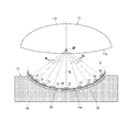
- FIG. 1 is a schematic cross-sectional view schematically showing a schematic configuration of an optical device according to a first embodiment
- FIG. 2 is a schematic cross-sectional view for explaining the relationship between light emitted from a solid-state light source and a lens.
- the optical device 10 of the present embodiment includes a lens 11, a plurality of solid-state light sources 12, and a substrate 13 on which the solid-state light source 12 is mounted.
- the lens 11 is an aspherical lens formed in a convex shape.
- the lens 11 may be a glass lens such as a glass mold lens or a resin lens such as a resin mold lens.
- the lens 11 has a light receiving surface 11a that receives light from the solid light source 12 and an emitting surface 11b that is incident from the light receiving surface 11a and emits refracted light, and the light receiving surface 11a and the emitting surface 11b have any convex shape. It is an aspherical surface.
- the lens 11 is a biconvex aspherical lens, but may be a plano-convex or meniscus-convex lens. Further, the curved surface may be spherical on either side or both sides.
- the solid light source 12 is a solid device that supplies energy such as electricity to a solid (substance) and emits light peculiar to the substance when excited.
- an LED is used.
- the solid-state light source 12 may be a semiconductor laser (LD) or an organic EL (OEL). Further, in the present embodiment, the plurality of solid-state light sources 12 are all LEDs that emit the same white light.
- the substrate 13 has a rigid base material 14 and a mounting surface 16 formed on the base material 14 in a curved surface shape substantially matching the focal plane shape of the lens 11 and on which a circuit pattern 15 is formed. ..
- the focal plane shape is an aspherical shape
- the mounting surface 16 is formed in an aspherical shape similar to the focal plane shape.
- the broken line indicated by the reference numeral S indicates the focal plane of the lens 11 with respect to a predetermined wavelength (here, e-line, 546 nm, green) as an average of white light.
- the focal plane S is formed in an aspherical shape, and when the exit surface of the solid light source 12 is the surface of the solid light source 12, it is at the same position as the surface of the solid light source 12, but in the present embodiment, the solid light source Since the exit surface of the solid light source 12 is recessed inward from the surface of the solid light source 12, the focal plane S is located at this position.
- the base material 14 is formed of a metal, ceramic, or high thermal conductive resin, and has a formed surface 14a formed in a curved surface shape substantially matching the focal surface shape of the lens 11. Further, the forming surface 14a is formed into an aspherical shape similar to the focal surface shape. Such a forming surface 14a may be formed at the same time when the base material 14 is manufactured, or the base material 14 having no forming surface 14a may be manufactured, and then the forming surface 14a may be formed. When the forming surface 14a is formed at the same time when the base material 14 is manufactured, the mold for forming the base material 14 is filled with a material such as molten metal or molten resin, and the formation provided on the mold is imparted.
- a material such as molten metal or molten resin
- the base material 14 having the forming surface 14a is formed by bringing the material into close contact with the surface (the surface for forming the forming surface 14a) and then demolding.
- the forming surface 14a is formed in a later step, the forming surface 14a is formed by processing a predetermined portion of the base material 14 by a processing means such as cutting or grinding.
- an insulating layer 20 having electrical insulating properties and having a surface as a mounting surface 16 is formed. Further, as described above, the mounting surface 16 is formed into a curved surface shape that substantially matches the shape of the focal plane surface of the lens 11, and the circuit pattern 15 is formed on the mounting surface 16.
- the thickness of the insulating layer 20 is preferably 0.01 mm to 5.0 mm. If the thickness of the insulating layer is thinner than 0.01 mm, there is a high possibility that the electrical insulation will be partially broken and short-circuited due to processing in the process of forming a circuit or the like, and the yield will be deteriorated.
- the thermal resistance of the insulating layer prevents the heat generated when the solid light source emits light from escaping to the base material 14, and deteriorates the long-term reliability of the solid light source.
- a base material 14 having a forming surface 14a is placed in a mold, and then a thermoplastic resin is injection-filled in the mold to form an insulating layer 20 made of the resin (insert molding).
- a method of filling a thermosetting resin and curing it in a mold to form it a method of filling and solidifying a thermoplastic resin or a thermosetting resin, and then performing post-processing such as cutting to form a mounting surface 16.
- post-processing such as cutting to form a mounting surface 16.
- the insulating layer there is also a method of forming the mounting surface 16 by cutting / grinding after spraying an aluminum oxide or an insulating ceramic layer on the base material 14.
- the insulating layer 20 is formed by applying a thermosetting resin material such as an epoxy material or a photopolymerizable material dissolved in an organic solvent with a dispenser, or by spraying to form an insulating layer, and then heat or It can also be formed by curing with light (ultraviolet rays).
- a thermosetting resin material such as an epoxy material or a photopolymerizable material dissolved in an organic solvent
- the surface of the forming surface 14a is porous by a chemical method such as etching with acid alkali, chemical conversion treatment, anodizing, or a physical method by dry or wet blasting.
- the surface shapes of the forming surface 14a and the lower surface of the insulating layer 20 may not be physically separated by roughening.
- the surface of the forming surface 14a may be subjected to plasma treatment to improve the adhesion between the forming surface 14a and the insulating layer 20.
- the insulating layer 20 insulates the circuit pattern 15 formed on the mounting surface 16 which is the upper surface (surface) thereof and the base material 14.
- thermoplastic resin having a high melting point and a thermosetting resin having solder reflow resistance.
- thermoplastic resin include aromatic polyamides such as 6T nylon (6TPA), 9T nylon (9TPA), 10T nylon (10TPA), 12T nylon (12TPA), MXD6 nylon (MXDPA), their alloy materials, and polyphenylene sulfide.
- Polyimide resin, heat-resistant acrylic, heat-resistant polyester, etc. can be used.
- thermosetting resin epoxy, silicone resin, urea resin (melamine resin, urea resin, etc.) and the like can be used.
- An inorganic filler may be added to these resins to increase the thermal conductivity.
- a conductive ink in which fine particles of silver and copper are dispersed in an organic binder or a conductive ink in which a conductive organic compound is dispersed in an organic solvent is used.
- a resist layer is formed on the surface, and patterning is performed using a circuit pattern mask and an exposure machine, or a circuit pattern is formed by etching after patterning with a direct drawing machine such as an electron beam or a laser, and metallized by vacuum film formation or plating.
- a method of forming a conductive layer by electrolysis or electroplating After forming a layer on the mounting surface 16 that suppresses the action of a catalyst that is the growth start point of electroless plating, this layer is physically removed by a laser or the like to remove the layer.
- a plurality of solid-state light sources 12 are mounted on the mounting surface 16 on which the circuit pattern 15 is formed, and are electrically connected to the circuit pattern 15.
- the substrate 13 is positioned with respect to the lens 11 so that the focal plane S of the lens 11 and the exit planes of the plurality of solid light sources 12 substantially coincide with each other. Further, as shown in FIG. 1, the line LC connecting the centers of the light emitting surfaces of the plurality of solid-state light sources 12 substantially coincides with the focal plane S of the lens 11 in the cross-sectional view, or the lens 11 with respect to the focal plane S.
- the substrate 13 is positioned with respect to the lens 11 so as to be located at positions separated from each other in the optical axis direction of the lens 11. In FIG.
- the connecting line LC is shown shifted from the focal plane S of the lens 11 in the cross-sectional view in the optical axis direction of the lens 11, but in reality, the connecting line LC is connected.
- the line LC substantially coincides with the focal plane S of the lens 11.
- the position separated from the focal plane S in the optical axis direction of the lens 11 means that the focal length of the lens 11 is f, and the "line LC connecting the centers of the light emitting surfaces of the plurality of solid light sources 12" and the lens 11
- the plurality of solid light sources 12 it is preferable to arrange the plurality of solid light sources 12 so as to be in the range of 0.5 ⁇ L / f ⁇ 2. This range is preferable because the divergence of light and the fluctuation of the amount of light can be suppressed. If L / f is less than 0.5, the degree of light divergence becomes too large, which is not preferable.
- L / f is larger than 2, the imaging position on the image side is too close to the light source side, and the amount of light fluctuates depending on the distance, which is not preferable.
- + Ln) / n) a plurality of the solid-state light sources 12 may be arranged at 0.5 ⁇ L / f ⁇ 2 with respect to the focal length f (focal length at the design wavelength) of the L and the lens 11. desirable.
- This range is preferable because the divergence of light and the fluctuation of the amount of light can be suppressed. Further, it is preferable to set this range because the divergence of light and the fluctuation of the amount of light can be suppressed. If L / f is less than 0.5, the degree of light divergence becomes too large, which is not preferable. If L / f is larger than 2, the imaging position on the image side is too close to the light source side, and the amount of light fluctuates depending on the distance, which is not preferable.
- the focal length differs depending on the wavelength or wavelength distribution of the solid-state light source 12, in the present embodiment, the wavelengths or wavelength distributions of the plurality of solid-state light sources 12 are the same, so that the mounting surface 16 has the wavelength (average wavelength, It is positioned with respect to the lens 11 according to (feature wavelength, etc.). That is, the substrate 13 is positioned with respect to the lens 11 so that the focal plane S of the lens 11 and the exit planes of the plurality of solid light sources 12 substantially coincide with each other, whereby the mounting surface 16 is adjusted to the wavelength. It is positioned with respect to the lens 11.
- the insulating layer 20 is provided on the surface of the base material 14, and the circuit pattern 15 is formed on the mounting surface 16 which is the surface of the insulating layer 20, but the lens 11 is not provided with the insulating layer 20.
- the circuit pattern 15 may be formed directly on the forming surface 14a of the base material 14 formed in a curved surface shape substantially matching the focal plane shape.
- the base material 14 may be formed of an electrical insulating material.
- the substrate 13 is manufactured as follows. That is, first, the base material 14 is placed in the mold, and then the insulating layer 20 is molded by insert molding (integral molding) in which a thermoplastic resin or a thermosetting resin is injection-filled in the mold.
- insert molding integral molding
- the line connecting the centers of the light emitting surfaces of the plurality of solid light sources 12 substantially coincides with the focal plane S of the lens 11 in the cross-sectional view, or the light of the lens 11 with respect to the focal plane S. It has a mounting surface 16 such that it exists at positions separated in the axial direction.
- the base material 14 may be formed in advance by injection molding, casting, or the like, and the formed surface 14a may be finished if necessary.
- the forming surface 14a of the base material 14 may be formed at the same time when the base material 14 is manufactured, or the base material 14 having no forming surface 14a may be manufactured and then the forming surface 14a may be formed.
- the surface of the forming surface 14a is subjected to, for example, chemical treatment such as nanomolding technology (NMT) or physical treatment such as blasting.
- NMT nanomolding technology
- blasting A concavo-convex layer and a porous layer may be formed by a specific treatment.
- the surface of the forming surface 14a may be subjected to plasma treatment using decompression plasma or atmospheric pressure plasma, or a coupling agent such as a silane coupling agent may be applied.
- a circuit pattern 15 formed of a plating film is formed on the surface of the insulating layer 20, that is, the mounting surface 16.
- the method for forming the circuit pattern 15 is not particularly limited, and a general-purpose method can be used. For example, a method of patterning a plating film with a photoresist and removing the plating film of a part other than the circuit pattern by etching, irradiating a part to form a circuit pattern with a laser beam to roughen the base material, or forming a functional group. Examples thereof include a method of applying the plating film to form a plating film only on the laser beam irradiated portion.
- the circuit pattern can also be formed by a method of patterning the conductive ink on the mounting surface using a dispenser or the like.
- each solid-state light source 12 is such that the angles ⁇ ( ⁇ 1, ⁇ 2, ⁇ 3) looking into the lens 11 when viewed from the normal direction of the emission surface are substantially equal. It is mounted on the mounting surface 16 so that the angle formed by the emission surfaces of all the solid-state light sources 12 and the tangent plane of the mounting surface 16 is within 20 milliradians. Further, as shown in FIG.
- each solid-state light source 12 when each solid-state light source 12 is mounted on the mounting surface 16 so that the normal NL of the exit surface passes through the front principal point (light source side principal point) MP of the lens 11 or its vicinity.
- the light emitted from the solid-state light source 12 can be taken out as irradiation light more efficiently.
- the mounting surface 16 is mounted as shown in FIG. 2B (a).
- each solid-state light source 12 has an angle ⁇ of 20 milliradians formed by the line connecting the center of each solid-state light source 12 and the main point MP and the normal of the emission surface of each solid-state light source 12. It is desirable to implement it within.
- the method of forming a shape in which the mounting position is defined in advance on the mounting surface 16 and mounting the solid-state light source on the shape is similarly effective in other embodiments.
- a plurality of solid-state light sources 12 may be arranged in parallel in three rows on the mounting surface 16 of the substrate 13, but the arrangement state due to the mounting of the solid-state light sources 12 is shown in FIG. It is not limited to what is shown. Since the mounting surface 16 is formed in a curved shape that substantially matches the shape of the focal plane of the lens 11, the solid light source 12 can be mounted at a desired (arbitrary) position of the mounting surface 16 so as to be in contact with the focal plane of the lens 11.
- the substrate 13 can be positioned with respect to the lens 11 so that the positions of the plurality of solid-state light sources 12 are substantially the same as the emission surfaces.
- the lens 11 When positioning the substrate 13 with respect to the lens 11, for example, the lens 11 is fixed to the case of an optical device 10 such as a lighting device, and then the substrate 13 is moved in contact with the lens 11 in the optical axis direction.
- the substrate 13 may be fixed to the case and then the lens 11 may be moved in contact with the substrate 13 in the optical axis direction, or both the substrate 13 and the lens 11 may be illuminated with each other. This may be done by moving the lens in contact with the axial direction.
- the manufacturing of the optical device 10 is completed by fixing the lens 11 and / or the substrate 13 to the case.
- FIG. 4 is a cross-sectional view showing a schematic configuration of the headlight 100 of the first example provided with the above-mentioned optical device 10.
- the optical device 10 includes a lens 11, a plurality of solid-state light sources 12, and a substrate 13 on which the solid-state light sources 12 are mounted.
- the substrate 13 includes a rigid base material 14 and an insulating layer 20 formed on the forming surface 14a of the base material 14, and the surface of the insulating layer 20 is a mounting surface 16.
- a circuit pattern 15 is formed on the mounting surface 16.
- the headlight 100 includes an optical device 10, a housing 101 in which the optical device 10 is housed, an outer lens 102 provided on the front surface side of the housing 101, and a reflector 103.
- the housing 101 is formed in a box shape with an opening on the front side, and an outer lens 102 is provided in the opening so as to face the lens 11 of the optical device 10.
- the reflector 103 includes a cup-shaped reflector main body 103a having a substantially U-shaped cross section and an inner surface as a reflective surface, and a support portion 103b for supporting and fixing the reflector main body 103a to the housing 101.
- the support portion 103b is formed in a cylindrical shape, a ring plate-shaped flange portion 103c is provided at the tip end portion (right end portion in FIG. 4), and the base end portion (left end portion in FIG. 4) is fixed to the bottom surface of the housing 101. Has been done.
- the lens 11 has an annular plate-shaped flange portion 11c on its outer peripheral portion, and by fixing the flange portion 11c to the flange portion 103c of the support portion 103b, the lens 11 is supported at a predetermined position of the housing 101. Has been done. Further, an opening for exposing the solid-state light source 12 of the optical device 10 is provided on the bottom surface of the reflector main body 103a. Further, a tubular holding wall 103d is provided at the bottom of the reflector main body 103a, and the substrate 13 is held inside the holding wall 103d. Further, an opening is provided in a part of the holding wall 103d, and a part of the base material 14 extends from the opening. A connector 105 is provided on the extending portion 14b, and the connector 105 and the circuit pattern 15 are connected by a wiring pattern 15d. The connector 105 and the power supply (not shown) are connected by a cable 106.
- a heat sink 110 is provided on the bottom of the housing 101.
- the heat sink 110 includes a heat sink main body 110a and a plurality of heat radiating fins 110b provided on the back surface side of the heat sink main body 110a.
- the heat sink body 110a is formed in a plate shape, and its surface is exposed inside the housing 101. Then, the base material 14 of the substrate 13 is in close contact with the surface of the exposed heat sink main body 110a. Therefore, a part of the heat generated from the solid light source 12 is transmitted to the heat sink main body 110a via the insulating layer 20 and the base material 14, and is dissipated to the outside by the heat radiating fins 110b, so that the solid light source 12 can be suppressed from overheating. ..
- FIG. 5 is a cross-sectional view showing a schematic configuration of the headlight 100A of the second example.
- the difference between the headlight 100A and the headlight 100 of the first example is the configuration of the substrate. Therefore, this point will be described below, and the same reference numerals are given to the same configuration as the headlight 100 of the first example. The explanation will be omitted.
- the substrate 13A of the headlight 100A of the second example includes a rigid base material 14A and an insulating layer 20A provided on the base material 14A.
- the base material 14A is formed of a high thermal conductive material and also has a function of a heat sink.
- the base material 14A is formed in a plate shape, its surface is exposed inside the housing 101, and a plurality of heat radiation fins 110b are provided on the back surface.
- the insulating layer 20A is formed of a high thermal conductive resin, and its surface has a mounting surface 16 formed of a curved surface shape substantially matching the focal plane shape of the lens 11 and a circuit pattern 15.
- the focal plane shape is an aspherical shape
- the mounting surface 16 is formed in an aspherical shape similar to the focal plane shape.
- the insulating layer 20A is held inside the tubular holding wall 103d provided at the bottom of the reflector main body 103a. An opening is provided in a part of the holding wall 103d, and a part of the insulating layer 20A extends from the opening.
- a connector 105 is provided on the extending portion 14b, and the connector 105 and the circuit pattern 15 are connected by a wiring pattern 15d.
- the connector 105 and the power supply (not shown) are connected by a cable 106.
- the base material 14A since the base material 14A also has the function of a heat sink, there is an advantage that the configuration is simpler than that of the headlight 100 of the first example.
- the substrate 13 has a mounting surface 16 formed on the insulating layer 20 formed on the rigid base material 14 in a curved shape substantially matching the focal surface shape of the lens 11.
- a plurality of solid-state light sources 12 are mounted on the mounting surface 16, and the substrate 13 is positioned with respect to the lens 11 so that the positions of the focal surface of the lens 11 and the exit surface of the solid-state light source 12 substantially coincide with each other. Therefore, the image plane curvature can be easily corrected so that the light emitted from the plurality of solid-state light sources 12 toward the lens 11 is emitted from the lens 11 as parallel light substantially parallel to the optical axis by the lens 11.
- the base material 14 is formed of metal, ceramic, or a highly thermally conductive resin, a part of the heat generated by the solid-state light source 12 is transferred to the base material 14 and can be dissipated from the base material 14, so that the solid-state light source 12 can be dissipated. Can suppress overheating.
- the base material 14 has a formed surface 14a formed in a curved surface shape substantially matching the focal surface shape of the lens 11, and an insulating layer 20 whose surface is a mounting surface 16 is formed on the formed surface 14a. Therefore, the surface of the insulating layer 20, that is, the mounting surface 16, can be easily formed into a curved surface shape that substantially matches the shape of the focal plane of the lens.
- the curved surfaces of the mounting surface 16 and the forming surface 14a are aspherical, the curvature of field can be easily corrected even when the lens 11 has the aspherical light receiving surface 11a and the emitting surface 11b.
- the solid-state light source 12 is mounted so that the angle ⁇ at which the lens 11 is seen from the normal direction of the emission surface is substantially equal, the light emitted from the solid-state light source 12 is effective. It is taken into the light receiving surface 11a of the lens 11 and can uniformly irradiate the lens 11.
- the solid-state light source 12 is mounted so that the angle formed by the emission surface and the tangent plane of the mounting surface 16 is within 20 milliradians, the solid-state light source 12 is mounted on the mounting surface 16 in a state close to the ideal. Can be implemented.
- the base material 14A and the heat radiation fins 110b may be formed together with the insulating layer 20.
- the LED and the LED lighting circuit are connected by a cable 106, but the power supply circuit for lighting the LED, a part, the figure, or the whole of the lighting circuit is placed in the vicinity of the connector 105 of the base material 14. You may provide it.
- the thickness of the wiring may be different depending on the current to be passed, the line width of the circuit depending on the size of the component to be mounted, and the distance between the adjacent wirings.
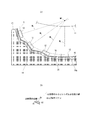
- FIG. 6 shows an optical device according to a second embodiment, and is a schematic cross-sectional view of a main part.
- the main difference between this embodiment and the first embodiment is that a plurality of insulating layers are laminated. Therefore, this point will be described below, and the same reference numerals will be given to the same configurations as those of the first embodiment. In some cases, the description thereof may be omitted.
- the above-mentioned insulating layer 20 is referred to as the first insulating layer 20.
- the first insulating layer 20 is formed on the forming surface 14a of the rigid base material 14, and the second insulating layer 22 is formed on the upper surface of the insulating layer 20. Further, a circuit pattern 15a is formed on the upper surface of the first insulating layer 20.
- the solid-state light source 12 is mounted on the mounting surface 16 which is the upper surface of the insulating layer 20, but in the present embodiment, the solid-state light source 12 is not mounted on the mounting surface 16. However, the solid-state light source 12 may be mounted on the mounting surface 16.
- the upper surface of the second insulating layer 22 is a mounting surface 16a, and the mounting surface 16a is formed in a curved surface shape that substantially matches the shape of the focal plane of the lens 11.
- the second insulating layer 22 has a mounting surface 16a such that it substantially coincides with the focal plane S1 of the lens 11 in cross-sectional view or exists at a position separated from the focal plane S1 in the optical axis direction of the lens 11. Have. Further, a circuit pattern 15b is formed on the mounting surface 16a. Then, the first solid-state light source 12a is mounted on the mounting surface 16a, and the solid-state light source 12a is electrically connected to the circuit pattern 15b.
- the position of the focal plane of the lens differs depending on the wavelength of the solid-state light source.
- the mounting surface 16a is positioned with respect to the lens 11. Although one first solid-state light source 12a is mounted on the mounting surface 16a in FIG. 6, it is actually mounted on the mounting surface 16a at a plurality of predetermined intervals. Further, the first solid-state light source 12a is exposed to an opening 23a formed in the third insulating layer 23, which will be described later, so as to taper from the mounting surface 16b of the insulating layer 23 toward the mounting surface 16a below the mounting surface 16b. After being arranged in such a manner, it is mounted on the mounting surface 16a.
- a through hole 30 is formed so as to penetrate the second insulating layer 22.
- a copper-plated film is formed on the inner surface of the through hole 30, and the circuit patterns 15a and 15b are electrically connected by the copper-plated film. Therefore, the first solid-state light source 12a mounted on the mounting surface 16a of the second insulating layer 22 is formed on the upper surface (mounting surface) 16 of the first insulating layer 20 via the circuit pattern 15b and the through hole 30. It is electrically connected to the circuit pattern 15a.
- a third insulating layer 23 is formed on the upper surface of the second insulating layer 22, that is, the mounting surface 16a.
- the upper surface of the third insulating layer 23 is a mounting surface 16b, and the mounting surface 16b is formed in a curved surface shape that substantially matches the shape of the focal plane of the lens 11.
- a circuit pattern 15c is formed on the mounting surface 16b.
- a second solid-state light source 12b is mounted on the mounting surface 16b, and the solid-state light source 12b is electrically connected to the circuit pattern 15c.
- the mounting surface 16b is positioned with respect to the lens 11 so that the focal surface S2 of the lens 11 with respect to the second solid light source 12b and the exit surface of the second solid light source 12b substantially coincide with each other.
- a through hole 31 is formed so as to penetrate the third insulating layer 23.
- a copper-plated film is formed on the inner surface of the through hole 31, and the circuit patterns 15b and 15c are electrically connected by the copper-plated film. Therefore, the second solid-state light source 12b mounted on the mounting surface 16b of the third insulating layer 23 is formed on the upper surface (mounting surface) 16a of the second insulating layer 22 via the circuit pattern 15c and the through hole 31. It is electrically connected to the circuit pattern 15b.
- the solid-state light sources 12a and 12b mounted on the mounting surfaces 16a and 16b have substantially equal angles ⁇ for viewing the lens 11 when viewed from the normal direction of the exit surface, as in the first embodiment. Is implemented. Further, all the solid-state light sources 12a and 12b are mounted so that the angle formed by the exit surface and the tangent plane of the mounting surfaces 16a and 16b is within 20 milliradians, as in the first embodiment. ..
- a plurality of solid-state light sources 12a and 12b are mounted on the mounting surfaces 16a and 16b. Then, the positions of the focal plane S1 of the lens 11 and the exit surfaces of the plurality of solid light sources 12a are substantially the same, and the positions of the focal plane S2 of the lens 11 and the exit surfaces of the plurality of solid light sources 12b are substantially the same.
- the substrate 13 is positioned with respect to the lens 11. Further, a position where the line connecting the centers of the light emitting surfaces of the plurality of solid light sources 12a substantially coincides with the focal plane S1 of the lens 11 in the cross-sectional view or is separated from the focal plane S1 in the optical axis direction of the lens 11. The substrate 13 is positioned with respect to the lens 11 so as to be present in.
- the line connecting the centers of the light emitting surfaces of the plurality of solid-state light sources 12b and 12b substantially coincides with the focal plane S2 of the lens 11 in the cross-sectional view, or is separated from the focal plane S2 in the optical axis direction of the lens 11.
- the substrate 13 is positioned with respect to the lens 11 so as to be present at the above-mentioned position. Further, since the focal length differs depending on the wavelength of the solid-state light source, the mounting surfaces 16a and 16b are positioned with respect to the lens 11 according to the wavelength.
- the positions of the focal plane S1 of the lens 11 and the exit surfaces of the plurality of solid light sources 12a are substantially the same, and the positions of the focal plane S2 of the lens 11 and the emission surfaces of the plurality of solid light sources 12b are substantially the same.
- the substrate 13 is positioned with respect to the lens 11, whereby the mounting surfaces 16a and 16b are positioned with respect to the lens 11 in accordance with the wavelength.
- the substrate 13 is manufactured as follows. That is, first, the base material 14 is placed in the mold, and then the first insulating layer 20 is molded by insert molding (integral molding) in which the thermoplastic resin or the thermosetting resin is injection-filled in the mold. ..
- the forming surface 14a is subjected to a chemical treatment such as nanomolding technology (NMT) to make the forming surface 14a uneven. Or it may be a porous surface.
- the forming surface 14a may be roughened by a physical method such as sandblasting.
- the surface of the forming surface 14a may be subjected to plasma treatment using decompression plasma or atmospheric pressure plasma, or a coupling agent such as a silane coupling agent may be applied.
- a circuit pattern 15a formed of a plating film is formed on the surface of the first insulating layer 20, that is, the mounting surface 16.
- the method for forming the circuit pattern 15a is not particularly limited, and a general-purpose method using the photoresist, laser light, or the like described above can be used.
- the insulating layer 20 is formed by applying a thermosetting resin material such as an epoxy material or a photopolymerizable material dissolved in an organic solvent with a dispenser or by spraying to form an insulating layer, and then heat or light ( It can also be formed by curing with ultraviolet rays).
- the second insulating layer 22 is applied to the substrate portion (mounting surface 16) provided with the base material 14, the first insulating layer 20 and the circuit pattern 15a by insert molding (integral molding), a dispenser, or spray coating. Along with molding, a through hole 30 is formed in the second insulating layer 22.
- the surface of the insulating layer 20 on which the circuit pattern is formed is subjected to plasma treatment using decompression plasma or atmospheric pressure plasma. May be applied.
- a coupling agent such as a silane coupling agent may be applied.
- a circuit pattern 15b formed of a plating film is formed on the surface of the second insulating layer 22, that is, the mounting surface 16a, and the circuit pattern 15b is electrically connected to the circuit pattern 15a via a through hole 30. do.
- the circuit pattern 15b is formed in the same manner as the circuit pattern 15a.
- insert molding (integral molding) is performed on the substrate portion (mounting surface 16a) provided with the base material 14, the first insulating layer 20, the second insulating layer 22, the circuit patterns 15a and 15b, and the through holes 30.
- a third insulating layer 23 is formed, and a through hole 31 is formed in the third insulating layer 23.
- plasma treatment using decompression plasma or atmospheric pressure plasma may be performed, or a silane coupling agent or the like may be applied. Coupling agent may be applied.
- a circuit pattern 15c formed of a plating film is formed on the surface of the third insulating layer 23, that is, the mounting surface 16b, and the circuit pattern 15c is electrically connected to the circuit pattern 15b via a through hole 31. do.
- the circuit pattern 15c is formed in the same manner as the circuit patterns 15a and 15b.
- the solid light source 12a is mounted on the mounting surface 16a, which is the surface of the second insulating layer 22, and is electrically connected to the circuit pattern 15, and is also mounted on the mounting surface 16b, which is the surface of the third insulating layer 23.
- a solid light source 12b is mounted and electrically connected to the circuit pattern 15c.
- the lens 11 When positioning the substrate 13 with respect to the lens 11, for example, the lens 11 is fixed to the case of an optical device 10A such as a lighting device, and then the substrate 13 is moved in contact with the lens 11 in the optical axis direction.
- the substrate 13 may be fixed to the case and then the lens 11 may be moved in contact with the substrate 13 in the optical axis direction, or both the substrate 13 and the lens 11 may be illuminated with each other. This may be done by moving the lens in contact with the axial direction.
- the lens 11 and / or the substrate 13 is fixed to the case to end the production of the optical device 10A.
- the second embodiment not only the same effect as that of the first embodiment can be obtained, but also the following effects can be obtained. Since the second insulating layer 22 and the third insulating layer 23 positioned with respect to the lens 11 are provided, the mounting surfaces 16a and 16b, which are the surfaces of the insulating layers 22 and 23, respectively, with respect to the lens 11. It will be positioned. Therefore, even when the solid-state light sources 12a and 12b having different wavelengths are appropriately mounted on the mounting surfaces 16a and 16b, the curvature of field can be easily corrected.
- circuit patterns 15a, 15b, 15c of the plurality of insulating layers 20, 22, 23 are selectively electrically connected by the through holes 30, 31, a plurality of circuit patterns 15b, 15c connected to the circuit patterns 15b, 15c.
- the lighting / extinguishing control of the solid-state light sources 12a and 12b can be easily performed. Further, if this method is used, a solid-state light source having the same emission wavelength or emission wavelength band is placed on the focal plane S with respect to the focal plane S of the lens 11, and if the light emitting surface is arranged on the focal plane S, the light is parallel light and the lens with respect to the focal plane S.
- a solid-state light source is placed in a direction away from 11, convergent light can be obtained, and conversely, if a solid-state light source is placed in a direction closer to the lens 11 than the focal plane S, diffused light can be obtained.
- a light source device capable of selecting parallel light, convergent light, and diffused light.
- the insulating layers are the first insulating layer 20, the second insulating layer 22, and the third insulating layer 23, but the number of layers of the insulating layer is two. It may be 4 layers or more. In the case of four or more layers, the steps of forming the next insulating layer on the third insulating layer, forming through holes as necessary, and forming a circuit pattern on the mounting surface which is the surface of the insulating layer are performed a predetermined number of times. By repeating the process, a plurality of four or more insulating layers can be formed.
- the circuit patterns 15a and 15b are electrically connected by the through holes 30, and the circuit patterns 15b and 15c are electrically connected by the through holes 31, but they are formed on the mounting surfaces of different insulating layers.
- the circuit patterns may be connected to each other by through-holes adjacent to each other in the thickness direction of the board 13, or circuit patterns arranged so as to sandwich one or more circuit patterns in the thickness direction of the board 13. May be connected by a through hole.
- the circuit patterns formed on the mounting surfaces of the plurality of insulating layers may be selectively electrically connected by through holes.
Landscapes
- Physics & Mathematics (AREA)
- Engineering & Computer Science (AREA)
- Optics & Photonics (AREA)
- General Engineering & Computer Science (AREA)
- General Physics & Mathematics (AREA)
- Microelectronics & Electronic Packaging (AREA)
- Mechanical Engineering (AREA)
- Mathematical Physics (AREA)
- Fastening Of Light Sources Or Lamp Holders (AREA)
- Led Device Packages (AREA)
- Non-Portable Lighting Devices Or Systems Thereof (AREA)
Priority Applications (4)
| Application Number | Priority Date | Filing Date | Title |
|---|---|---|---|
| JP2022506006A JP7554256B2 (ja) | 2020-03-13 | 2021-03-04 | 光学装置、光学装置の製造方法および前照灯 |
| CN202180020763.0A CN115335630A (zh) | 2020-03-13 | 2021-03-04 | 光学装置、光学装置的制造方法以及前照灯 |
| US17/910,973 US11865964B2 (en) | 2020-03-13 | 2021-03-04 | Optical apparatus, method for manufacturing optical apparatus, and headlight |
| JP2024079894A JP7716534B2 (ja) | 2020-03-13 | 2024-05-16 | 光学装置、光学装置の製造方法および前照灯 |
Applications Claiming Priority (2)
| Application Number | Priority Date | Filing Date | Title |
|---|---|---|---|
| JP2020043856 | 2020-03-13 | ||
| JP2020-043856 | 2020-03-13 |
Publications (1)
| Publication Number | Publication Date |
|---|---|
| WO2021182303A1 true WO2021182303A1 (ja) | 2021-09-16 |
Family
ID=77670872
Family Applications (1)
| Application Number | Title | Priority Date | Filing Date |
|---|---|---|---|
| PCT/JP2021/008488 Ceased WO2021182303A1 (ja) | 2020-03-13 | 2021-03-04 | 光学装置、光学装置の製造方法および前照灯 |
Country Status (4)
| Country | Link |
|---|---|
| US (1) | US11865964B2 (https=) |
| JP (2) | JP7554256B2 (https=) |
| CN (1) | CN115335630A (https=) |
| WO (1) | WO2021182303A1 (https=) |
Cited By (1)
| Publication number | Priority date | Publication date | Assignee | Title |
|---|---|---|---|---|
| JP2023130584A (ja) * | 2022-03-08 | 2023-09-21 | マクセル株式会社 | 光学装置、撮像システムおよび移動体 |
Citations (8)
| Publication number | Priority date | Publication date | Assignee | Title |
|---|---|---|---|---|
| JPH08130301A (ja) * | 1994-01-31 | 1996-05-21 | Kyocera Corp | 画像装置 |
| JP2001213322A (ja) * | 2000-02-01 | 2001-08-07 | Sankosha:Kk | 鉄道信号灯 |
| JP2001266620A (ja) * | 2000-03-01 | 2001-09-28 | Robert Bosch Gmbh | 車両用の照明装置 |
| JP2004214144A (ja) * | 2003-01-08 | 2004-07-29 | Mitsubishi Electric Corp | 前照灯 |
| JP2004327188A (ja) * | 2003-04-23 | 2004-11-18 | Koito Mfg Co Ltd | 車両用前照灯 |
| JP2011171002A (ja) * | 2010-02-16 | 2011-09-01 | Koito Mfg Co Ltd | 光学ユニット |
| US20150377453A1 (en) * | 2014-06-27 | 2015-12-31 | Samsung Electronics Co., Ltd. | Light emitting module |
| US20190113199A1 (en) * | 2017-10-16 | 2019-04-18 | Valeo Vision | Lighting module for motor vehicle |
Family Cites Families (8)
| Publication number | Priority date | Publication date | Assignee | Title |
|---|---|---|---|---|
| BR112014003829A2 (pt) * | 2011-08-24 | 2017-03-14 | Koninklijke Philips Nv | dispositivo autoestereoscópico de exibição, método para exibir imagens autoestereoscópicas e método de fabricação de um dispositivo autoestereoscópico de exibição |
| JP5723497B2 (ja) * | 2013-03-28 | 2015-05-27 | 東芝ホクト電子株式会社 | 発光装置の製造方法 |
| US10363860B2 (en) * | 2013-12-12 | 2019-07-30 | Mitsubishi Electric Corporation | Headlight module and headlight apparatus |
| JP2017157669A (ja) | 2016-03-01 | 2017-09-07 | 三菱電機株式会社 | 電子機器及びその製造方法 |
| KR102386513B1 (ko) * | 2016-08-05 | 2022-04-22 | 서울바이오시스 주식회사 | 발광소자 |
| TWI607179B (zh) * | 2016-11-30 | 2017-12-01 | 隆達電子股份有限公司 | 透鏡陣列、使用透鏡陣列的車燈透鏡組及使用車燈透鏡組的車燈總成 |
| JP6975603B2 (ja) * | 2017-09-27 | 2021-12-01 | 京セラ株式会社 | 発光装置 |
| FR3085903B1 (fr) * | 2018-09-19 | 2021-06-25 | Valeo Vision | Systeme lumineux pour dispositif d'eclairage et/ou de signalisation d'un vehicule automobile |
-
2021
- 2021-03-04 US US17/910,973 patent/US11865964B2/en active Active
- 2021-03-04 CN CN202180020763.0A patent/CN115335630A/zh active Pending
- 2021-03-04 WO PCT/JP2021/008488 patent/WO2021182303A1/ja not_active Ceased
- 2021-03-04 JP JP2022506006A patent/JP7554256B2/ja active Active
-
2024
- 2024-05-16 JP JP2024079894A patent/JP7716534B2/ja active Active
Patent Citations (8)
| Publication number | Priority date | Publication date | Assignee | Title |
|---|---|---|---|---|
| JPH08130301A (ja) * | 1994-01-31 | 1996-05-21 | Kyocera Corp | 画像装置 |
| JP2001213322A (ja) * | 2000-02-01 | 2001-08-07 | Sankosha:Kk | 鉄道信号灯 |
| JP2001266620A (ja) * | 2000-03-01 | 2001-09-28 | Robert Bosch Gmbh | 車両用の照明装置 |
| JP2004214144A (ja) * | 2003-01-08 | 2004-07-29 | Mitsubishi Electric Corp | 前照灯 |
| JP2004327188A (ja) * | 2003-04-23 | 2004-11-18 | Koito Mfg Co Ltd | 車両用前照灯 |
| JP2011171002A (ja) * | 2010-02-16 | 2011-09-01 | Koito Mfg Co Ltd | 光学ユニット |
| US20150377453A1 (en) * | 2014-06-27 | 2015-12-31 | Samsung Electronics Co., Ltd. | Light emitting module |
| US20190113199A1 (en) * | 2017-10-16 | 2019-04-18 | Valeo Vision | Lighting module for motor vehicle |
Cited By (1)
| Publication number | Priority date | Publication date | Assignee | Title |
|---|---|---|---|---|
| JP2023130584A (ja) * | 2022-03-08 | 2023-09-21 | マクセル株式会社 | 光学装置、撮像システムおよび移動体 |
Also Published As
| Publication number | Publication date |
|---|---|
| CN115335630A (zh) | 2022-11-11 |
| US20230139866A1 (en) | 2023-05-04 |
| JP7554256B2 (ja) | 2024-09-19 |
| JP7716534B2 (ja) | 2025-07-31 |
| JPWO2021182303A1 (https=) | 2021-09-16 |
| US11865964B2 (en) | 2024-01-09 |
| JP2024109704A (ja) | 2024-08-14 |
Similar Documents
| Publication | Publication Date | Title |
|---|---|---|
| EP1730792B1 (en) | Manufacturing method of led mounting module, and manufacturing method of led module | |
| US20050174779A1 (en) | Light emitting diode and method for fabricating the same | |
| US10634329B2 (en) | Lamp unit and manufacturing method thereof | |
| JP5766122B2 (ja) | 発光手段の製造方法 | |
| JP2004520612A (ja) | 光導波路をエレクトロオプティックもしくはオプトエレクトリックな半導体コンバータに光学的に結合するための結合装置 | |
| US20220190464A1 (en) | Component Carrier Having at Least a Part Formed as a Three-Dimensionally Printed Structure Forming an Antenna | |
| JP2012525689A5 (https=) | ||
| TW201414015A (zh) | 發光二極體封裝以及用於製造其之方法 | |
| KR20090033907A (ko) | 다수의 방사선 방사 구성요소들을 포함하는 방사선 방사 장치 및 조명 장치 | |
| KR102668526B1 (ko) | 몰드 회로 기판 | |
| JP7716534B2 (ja) | 光学装置、光学装置の製造方法および前照灯 | |
| JP2012525689A (ja) | レンズ及び印刷されたリフレクタ面を有する回路基板の製造方法並びにその方法により製造される回路基板 | |
| US20200045832A1 (en) | 3d printing method and product | |
| JP6489843B2 (ja) | 光源ユニット | |
| JP3708108B2 (ja) | 光照射装置及び光学ユニット | |
| JP6830583B2 (ja) | 配線部品の製造方法 | |
| JP3901067B2 (ja) | 光通信モジュールおよびその製造方法 | |
| US20130250576A1 (en) | Wiring board device, luminaire and manufacturing method of the wiring board device | |
| US10779412B2 (en) | Lighting assembly with high irradiance | |
| CN114335307B (zh) | 发光模块 | |
| KR101831771B1 (ko) | 광원모듈, 광원모듈의 제조방법, 및 이를 포함하는 조명기기 | |
| JP7209214B2 (ja) | 車両用照明装置、および車両用灯具 | |
| JPWO2021182303A5 (https=) | ||
| JP2023130584A (ja) | 光学装置、撮像システムおよび移動体 | |
| JP2023065765A (ja) | 車両用照明装置、車両用灯具、および車両用照明装置の製造方法 |
Legal Events
| Date | Code | Title | Description |
|---|---|---|---|
| 121 | Ep: the epo has been informed by wipo that ep was designated in this application |
Ref document number: 21768346 Country of ref document: EP Kind code of ref document: A1 |
|
| ENP | Entry into the national phase |
Ref document number: 2022506006 Country of ref document: JP Kind code of ref document: A |
|
| NENP | Non-entry into the national phase |
Ref country code: DE |
|
| 122 | Ep: pct application non-entry in european phase |
Ref document number: 21768346 Country of ref document: EP Kind code of ref document: A1 |