WO2021182034A1 - 導電ペーストおよびそれを用いた導電パターン - Google Patents
導電ペーストおよびそれを用いた導電パターン Download PDFInfo
- Publication number
- WO2021182034A1 WO2021182034A1 PCT/JP2021/005749 JP2021005749W WO2021182034A1 WO 2021182034 A1 WO2021182034 A1 WO 2021182034A1 JP 2021005749 W JP2021005749 W JP 2021005749W WO 2021182034 A1 WO2021182034 A1 WO 2021182034A1
- Authority
- WO
- WIPO (PCT)
- Prior art keywords
- silver
- conductive paste
- electroconductive
- pattern
- conductive
- Prior art date
- Legal status (The legal status is an assumption and is not a legal conclusion. Google has not performed a legal analysis and makes no representation as to the accuracy of the status listed.)
- Ceased
Links
Images
Classifications
-
- H—ELECTRICITY
- H01—ELECTRIC ELEMENTS
- H01B—CABLES; CONDUCTORS; INSULATORS; SELECTION OF MATERIALS FOR THEIR CONDUCTIVE, INSULATING OR DIELECTRIC PROPERTIES
- H01B1/00—Conductors or conductive bodies characterised by the conductive materials; Selection of materials as conductors
- H01B1/20—Conductive material dispersed in non-conductive organic material
- H01B1/22—Conductive material dispersed in non-conductive organic material the conductive material comprising metals or alloys
-
- H—ELECTRICITY
- H01—ELECTRIC ELEMENTS
- H01B—CABLES; CONDUCTORS; INSULATORS; SELECTION OF MATERIALS FOR THEIR CONDUCTIVE, INSULATING OR DIELECTRIC PROPERTIES
- H01B1/00—Conductors or conductive bodies characterised by the conductive materials; Selection of materials as conductors
-
- H—ELECTRICITY
- H01—ELECTRIC ELEMENTS
- H01B—CABLES; CONDUCTORS; INSULATORS; SELECTION OF MATERIALS FOR THEIR CONDUCTIVE, INSULATING OR DIELECTRIC PROPERTIES
- H01B5/00—Non-insulated conductors or conductive bodies characterised by their form
- H01B5/14—Non-insulated conductors or conductive bodies characterised by their form comprising conductive layers or films on insulating-supports
Definitions
- the present invention relates to, for example, a conductive paste used for forming a conductive pattern such as an electrode of an electronic device and a conductive pattern using the conductive paste.
- semiconductor elements semiconductor elements such as ICs and LSIs on metal pieces called lead frames and fixing them, forming circuits on substrates by printing, etc., or forming electrodes for electronic components such as capacitors.
- conductive pastes are used for various purposes.
- the conductive paste has less variation in line width, and circuit patterns can be printed with high accuracy. Even in the circuit pattern, it is required to have high electrical conductivity and thermal conductivity, high migration resistance, and excellent workability by having appropriate viscosity and fluidity. There is.
- Patent Document 1 silver fine particles having an average primary particle diameter of 10 nm or more and 200 nm or less are added to silver particles having an average particle diameter of 0.5 ⁇ m or more to reduce the fluidity of the conductive paste.
- a conductive paste that can form a conductive film wiring having a low volume resistance by suppressing the particles, and has improved adhesion to a substrate and printability.
- Patent Document 2 Japanese Patent Application Laid-Open No. 2019-102273
- three types of fillers containing nanoparticles are used so as to have an appropriate viscosity that can maintain a fine wire shape while maintaining an electrically low resistance.
- a conductive paste in which a decrease in viscosity is suppressed is disclosed.
- An object of the present invention is to provide a conductive paste having excellent workability by having an appropriate viscosity and fluidity, and a conductive pattern (circuit pattern) using the conductive paste.
- the present inventors are effective in suppressing the occurrence of line width variation and migration due to bleeding during printing, and are conductive for realizing high electrical conductivity and excellent workability.
- the above-mentioned problems were solved by adding silver-coated silica powder to the base of silver-coated copper flakes as the conductive paste. We have found that we can solve the problem, and have completed the present invention.
- a conductive paste containing silver-coated copper flakes, silver-coated silica powder, and a conductive pattern using the same are provided.
- the conductive paste of the present invention may further contain a binder resin, a solvent, and a curing agent.
- the conductive paste of the present invention is a composition formed into a paste by adding silver-coated copper flakes and silver-coated silica powder, and a binder resin to them. As long as the silver-coated copper flakes, the silver-coated silica powder, and the binder resin are contained, other components such as a solvent and a defoaming agent may be contained as needed, as long as the effects of the present invention are not impaired. good.
- the silver-coated copper flakes used in the present invention are not particularly limited as long as they are silver-coated flake-shaped copper powders, and known ones can be used.
- the volume average particle size (D 50 ) of the silver-coated copper flakes is preferably 1.0 ⁇ m or more and 50 ⁇ m or less, and more preferably 2.0 ⁇ m or more and 20 ⁇ m or less. In particular, when the volume average particle size (D 50 ) of the silver-coated copper flakes is 2.0 ⁇ m or more and 20.0 ⁇ m or less, it becomes extremely easy to deal with fine lines when drawing a circuit.
- the copper powder coated with silver spherical or substantially spherical copper powder or flake-shaped copper powder is known, but it suppresses the decrease of electrical contacts after circuit formation and increases the electrical resistance. From the viewpoint of suppressing, it is preferable to use silver-coated copper flakes in the present invention.
- the silver-coated copper flakes may be completely coated with silver, or the copper may be partially exposed. It is preferable to completely cover with silver because the specific resistance value becomes small.
- the blending amount of the silver-coated copper flakes is preferably 10% by volume or more and 40% by volume or less, and more preferably 30% by volume or more and 40% by volume or less with respect to the total non-volatile content of the conductive paste. When the blending amount of the silver-coated copper flakes is 10% by volume or more and 40% by volume or less, workability can be improved by having an appropriate viscosity and fluidity while keeping the specific resistance value low.
- the silver-coated silica powder used in the present invention is not particularly limited as long as it is a silver-coated silica powder, and known ones can be used.
- the volume average particle size (D 50 ) of the silver-coated silica powder is preferably 0.050 ⁇ m or more and 50.0 ⁇ m or less, and more preferably 0.1 ⁇ m or more and 5.0 ⁇ m or less.
- the volume average particle size (D 50 ) of the silver-coated silica powder is 0.1 ⁇ m or more and 5.0 ⁇ m or less, the specific resistance value can be suppressed low by achieving a high filling rate.
- the silver-coated silica powder may be completely coated with silver, or the silica may be partially exposed. It is preferable to completely cover with silver because the specific resistance value becomes small.
- the blending amount of the silver-coated silica powder is preferably in the range of 99: 1 to 15:85, preferably in the range of 99: 1 to 20:80, in the volume ratio of the silver-coated copper flakes and the silver-coated silica powder. More preferred.
- the volume ratio of the silver-coated copper flakes to the silver-coated silica powder is in the range of 99: 1 to 15:85, the fluidity of the obtained conductive paste becomes particularly suitable, and the variation of the lines during printing becomes small. In addition, the electrical conductivity and migration resistance of the formed circuit pattern are also improved. Further, the shape of the silver-coated silica powder can be used without particular limitation as long as it is a particle. If it is in the form of particles, it is particularly preferably used because it has excellent fluidity.
- thermosetting resin examples include epoxy resin, phenol resin, urea resin, unsaturated polyester resin, alkyd resin, polyurethane, and thermosetting polyimide.
- thermoplastic resin such as polyethylene, polypropylene, polystyrene, polyvinyl chloride, polyester, or polyamide in which a functional group remains at the terminal may be used in combination with a curing agent.
- the resin binder may be blended in a ratio of 30% by volume or more and 60% by volume or less with respect to the total non-volatile content of the conductive paste. preferable.
- the solvent used for the conductive paste of the present invention is not particularly limited. It can be appropriately selected depending on the solubility of the resin to be used, the type of printing method, and the like.
- Examples of the solvent of the present invention include one or two kinds such as ester solvent, ketone solvent, glycol ether solvent, aliphatic solvent, alicyclic solvent, aromatic solvent, alcohol solvent, water and the like. An example is a mixture of the above.
- ester solvent examples include ethyl acetate, isopropyl acetate, n-butyl acetate, isobutyl acetate, amyl acetate, ethyl lactate, dimethyl carbonate and the like.
- ketone solvent examples include acetone, methyl ethyl ketone, methyl isobutyl ketone benzene, diisobutyl ketone, diacetone alcohol, isophorone, cyclohexanenon and the like.
- Glycol ether-based solvents include ethylene glycol monoethyl ether, ethylene glycol monoisopropyl ether, ethylene glycol monobutyl ether, and other monoethers such as acetate, diethylene glycol dimethyl ether, diethylene glycol diethyl ether, diethylene glycol monoethyl ether, diethylene glycol monobutyl ether, and propylene. Examples thereof include glycol monomethyl ether, propylene glycol monoethyl ether and the like, and acetate esters of these monoethers.
- examples of the aliphatic solvent include n-heptane, n-hexane, isohexane, isoheptane and the like.
- examples of the alicyclic solvent include methylcyclohexane, ethylcyclohexane, cyclohexane and the like.
- aromatic solvents include toluene, xylene, tetralin and the like.
- alcohol-based solvents (excluding the above-mentioned glycol ether-based solvents) include ethanol, propanol, butanol and the like.
- the conductive paste of the present invention has excellent workability because it has an appropriate viscosity and an appropriate fluidity, and has excellent line width variation and can print a circuit pattern with high accuracy. In addition to being effective, it also has an excellent effect of having high electrical conductivity and high migration resistance even in a printed conductive pattern.
- the conductive paste according to the embodiment of the present invention and the conductive paste of the comparative example were produced under the following raw materials and conditions (see “Table 1”).
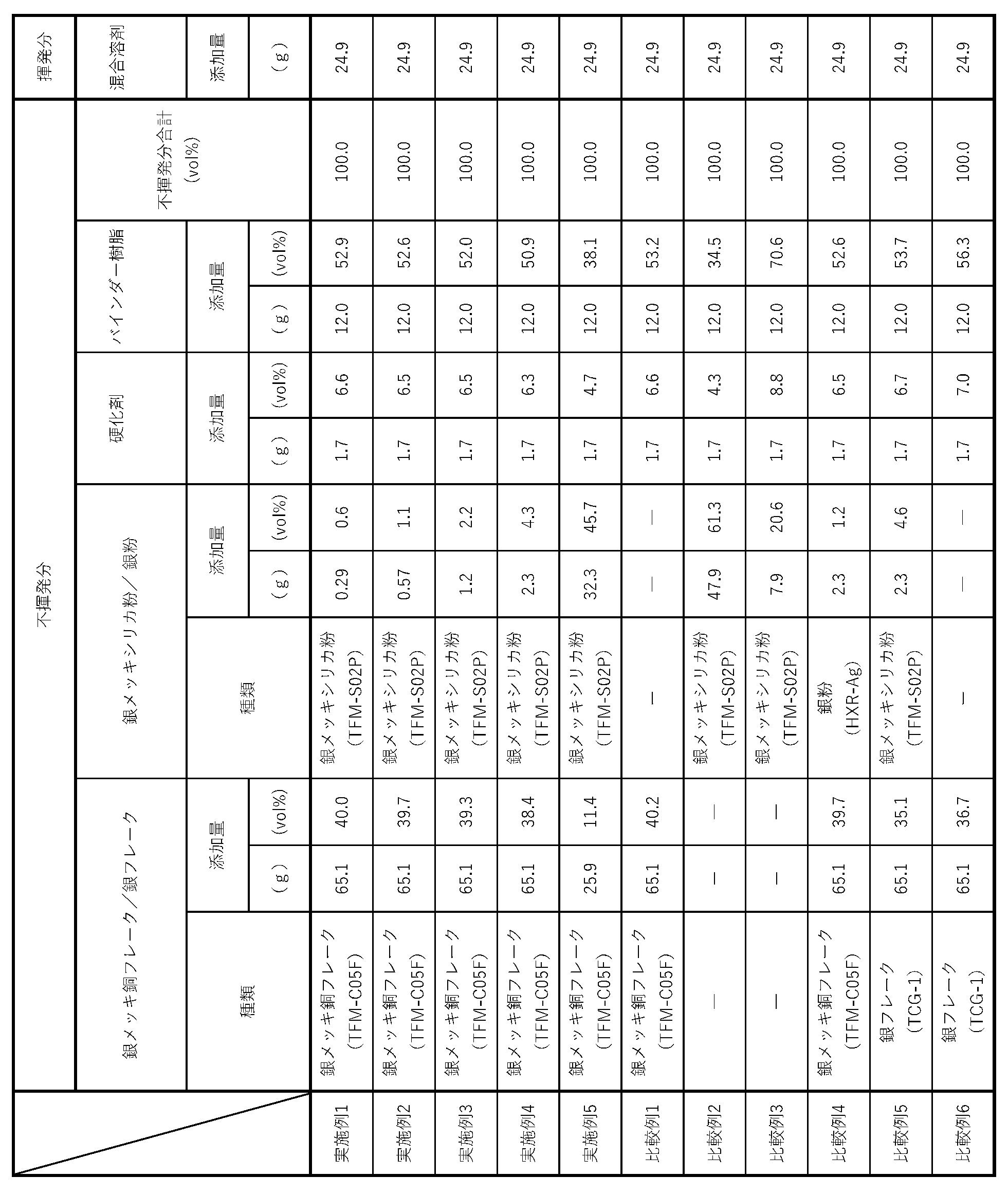
- Table 1 65.1 g of Toyaltec Filler (registered trademark) / TFM-C05F (manufactured by Toyo Aluminum K.K.) with a volume average particle diameter (D 50 ) of 6 ⁇ m as silver-coated copper flakes, and volume average particle diameter as silver-coated silica powder.
- Example 1 0.29 g of Toyal Tech Filler (registered trademark) / TFM-S02P (manufactured by Toyo Aluminum K.K.) with (D 50 ) of 2 ⁇ m, and 12 of Elitel (registered trademark) / UE-3210 (manufactured by Unitica) as a binder resin. .0 g, 1.7 g of blocked isocyanate (product name: 7992, manufactured by Baxenden) as a curing agent, and 24.9 g of a mixed solvent in which ethylcarbitol acetate and isophorone are mixed at a weight ratio of 16: 9 as a solvent. Then, the conductive paste of Example 1 was produced by kneading with a disper and three rolls.
- Example 2 Same as Example 1 except that 0.57 g of Toyaltec Filler (registered trademark) / TFM-S02P (manufactured by Toyo Aluminum K.K.) having a volume average particle diameter (D 50) of 2 ⁇ m was blended as the silver-coated silica powder.
- the conductive paste of Example 2 was produced under the conditions.
- Example 3 Same as Example 1 except that 1.2 g of Toyaltec Filler (registered trademark) / TFM-S02P (manufactured by Toyo Aluminum K.K.) having a volume average particle diameter (D 50) of 2 ⁇ m was blended as the silver-coated silica powder.
- the conductive paste of Example 3 was produced under the conditions.
- Example 4 Same as Example 1 except that 2.3 g of Toyaltec Filler (registered trademark) / TFM-S02P (manufactured by Toyo Aluminum K.K.) having a volume average particle diameter (D 50) of 2 ⁇ m was blended as the silver-coated silica powder.
- the conductive paste of Example 4 was produced under the conditions.
- Example 5 25.9 g of Toyaltec Filler (registered trademark) / TFM-C05F (manufactured by Toyo Aluminum K.K.) with a volume average particle diameter (D 50 ) of 6 ⁇ m as silver-coated copper flakes, and volume average particle diameter as silver-coated silica powder.
- the conductive paste of Example 5 was prepared under the same conditions as in Example 1 except that 32.3 g of Toyaltec Filler (registered trademark) / TFM-S02P (manufactured by Toyo Aluminum K.K.) having a volume of 2 ⁇ m (D 50) was blended. I made it.
- Comparative Example 1 The conductive paste of Comparative Example 1 was produced under the same conditions as in Example 1 except that the silver-coated silica powder was not blended.
- Comparative Example 2 47.9 g of Toyaltec Filler (registered trademark) / TFM-S02P (manufactured by Toyo Aluminum K.K.) with a volume average particle diameter (D 50 ) of 2 ⁇ m was blended as silver-coated silica powder without blending silver-coated copper flakes. Except for this, the conductive paste of Comparative Example 2 was produced under the same conditions as in Example 1.
- Comparative Example 3 7.9 g of Toyaltec Filler (registered trademark) / TFM-S02P (manufactured by Toyo Aluminum K.K.) with a volume average particle diameter (D 50 ) of 2 ⁇ m was blended as silver-coated silica powder without blending silver-coated copper flakes. Except for this, the conductive paste of Comparative Example 3 was produced under the same conditions as in Example 1.
- Comparative Example 4 Examples except that 2.3 g of spherical silver powder (product name: HXR-Ag, manufactured by Nippon Atomize Processing Co., Ltd.) having a volume average particle diameter (D 50 ) of 5.7 ⁇ m was blended as an alternative to the silver-coated silica powder.
- the conductive paste of Comparative Example 4 was produced under the same conditions as in 1.
- Comparative Example 5 As an alternative to silver-coated copper flakes, 65.1 g of silver flakes with a volume average particle diameter (D 50 ) of 4.8 ⁇ m (product name: TCG-1 manufactured by Tokuri Kagaku Kenkyusho Co., Ltd.) were used as silver-coated silica powder. , Comparative Example under the same conditions as in Example 1 except that 2.3 g of Toyaltec Filler (registered trademark) / TFM-S02P (manufactured by Toyo Aluminum K.K.) having a volume average particle diameter (D 50) of 2 ⁇ m was blended. The conductive paste of No. 5 was produced.
- Toyaltec Filler registered trademark
- TFM-S02P manufactured by Toyo Aluminum K.K.
- Comparative Example 6 As an alternative to silver-coated copper flakes, 65.1 g of silver flakes with a volume average particle size (D 50 ) of 4.8 ⁇ m (product name: TCG-1 is manufactured by Tokuriki Kagaku Kenkyusho Co., Ltd.) are blended and silver-coated silica. The conductive paste of Comparative Example 6 was produced under the same conditions as in Example 1 except that no powder was blended.
- Table 1 shows the addition amount (g) of each component blended in the conductive pastes of Examples 1 to 5 and Comparative Examples 1 to 6 and the blending ratio (Vol%) of each component to the total non-volatile content of the conductive paste.
- circuit pattern (conductive pattern) Using the conductive pastes of Examples 1 to 5 and Comparative Examples 1 to 6, the material is stainless steel, the number of screen meshes is 325 mesh, the emulsion thickness is 10 ⁇ m, the line width is 100 ⁇ m, and the distance between each line is 100 ⁇ m.
- a screen printing machine product name: DP-320 type screen printing machine, manufactured by Neurongue Precision Industry Co., Ltd.
- the sheet on which the circuit pattern was printed was dried at 150 ° C. for 30 minutes to prepare a circuit pattern for evaluation.
- Viscosity In order to investigate the relationship between the workability and bleeding property of the conductive paste, the viscosities of the conductive pastes of Examples 1 to 5 and Comparative Examples 1 to 6 were measured with a B-type viscometer (model number). : DV2THBCJ0, manufactured by Brookfield Co., Ltd.) was measured under the conditions of a temperature of 25 ° C. and a rotation speed of 0.5 rpm. The results are shown in Table 2.
- the variation in the line width of the circuit pattern is preferable as the value of 3 ⁇ is smaller, but if the value of 3 ⁇ exceeds 50 ⁇ m, adjacent lines may be short-circuited when energized, etc. It was evaluated as “defective), and when it was 50 ⁇ m or less, it was evaluated as “ ⁇ ” (good). When a short circuit (contact) was observed in a part of adjacent lines from the beginning of circuit pattern formation, it was evaluated as "x" (defective) regardless of the value of 3 ⁇ . The above results are shown in Table 2.
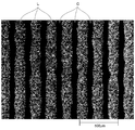
- FIG. 1 a photomicrograph of the circuit pattern produced using the conductive paste of Example 4 is shown in FIG. 1
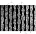
- a photomicrograph of the circuit pattern produced using the conductive paste of Comparative Example 1 is shown in FIG.
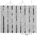
- FIG. 2 and FIG. 3 show a photomicrograph of a circuit pattern produced using the conductive paste of Comparative Example 3.
- the migration resistance of the circuit pattern is determined by holding each evaluation circuit pattern of the upper technique under the conditions of 85 ° C., humidity 85%, and applied voltage 50V, and measuring the time until a short circuit occurs. Was evaluated by. The presence or absence of a short circuit in the circuit pattern was confirmed using a migration tester (product name: MODEL MIG-87B, manufactured by IMV Co., Ltd.).
- the migration resistance indicates that the longer the time until the circuit pattern is short-circuited, the better the migration resistance.
- the case where the time until the short-circuit occurs is 800 hours or more is defined as “ ⁇ ”. "(Good) was evaluated, and when it was less than 800 hours, it was evaluated as” x "(bad). The above results are shown in Table 2.
- the specific resistance value ( ⁇ ⁇ cm) of the circuit pattern is for evaluation made in a 4.8 cm ⁇ 4.8 cm square shape with a material of polyester resin, 280 screen meshes, and an emulsion thickness of 9 microns.
- the conductive paste was printed on a PET film and dried at 150 ° C. for 30 minutes to form a coating film.
- the thickness of the coating film was confirmed by measuring with a Digimatic standard outside micrometer (trade name: IP65 COOLANT PROOF Micrometer, manufactured by Mitutoyo Co., Ltd.). It was confirmed by measuring with a 4-probe type surface resistance measuring instrument (trade name: Loresta GP, manufactured by Mitsubishi Analytech Co., Ltd.).
- the conductor layer is the value obtained by inputting the dimensions of the printed matter, the average thickness of the printed matter, and the coordinates of the measurement points into the above-mentioned 4-probe type surface resistivity measuring device and automatically calculating them. / Conductive pattern) specific resistance value.
- the size of the printed matter refers to the dimension consisting of the maximum length and the maximum width of the pattern of the predetermined shape of the printed matter. Resistivity indicates that the smaller the better, 2.0 if ⁇ exhibited the following 10 -4 ⁇ ⁇ cm was evaluated as " ⁇ " (good), contrary to 2.0 ⁇ 10 - A case larger than 4 ⁇ ⁇ cm was evaluated as “x” (defective). The above results are shown in Table 2.
- Table 2 shows the evaluation of the conductive pastes of Examples 1 to 5 and Comparative Examples 1 to 6 and the circuit patterns (conductive patterns) produced using them.
- the conductive paste of the present invention is based on silver-coated copper flakes, to which silver-coated silica powder is added. By doing so, good results can be obtained in any of the evaluations of "line width variation", “migration resistance” and “specific resistance value” of the printed circuit pattern (conductive pattern), and as a result, good results can be obtained. There is little variation in line width, it is possible to print a conductive pattern with high accuracy, and even in the printed conductive pattern, it has high electrical and thermal conductivity, high migration resistance, and 30 Pa. -It was found that excellent workability was provided by having a viscosity of s or more and 70 Pa ⁇ s or less.
- the volume ratio of the silver-coated copper flakes to the silver-coated silica powder is preferably in the range of 99: 1 to 15:85.
- the volume ratio of the silver-coated copper flakes to the silver-coated silica powder is in the range of 99: 1 to 90:10, as in the conductive paste, more excellent migration resistance can be obtained.
- the blending amount of the silver-coated copper flakes was set to 10% by volume or more and 40% by volume or less with respect to the total non-volatile content of the conductive paste, so that the printed circuit pattern could be used.
- the variation in line width is small, excellent migration resistance and conductivity can be obtained, and workability can be improved by having an appropriate viscosity and fluidity while keeping the specific resistance value low.
- the blending amount of the silver-coated copper flakes is 30% by volume or more and 40% by volume or less with respect to the total non-volatile content of the conductive paste, more excellent migration resistance can be obtained. It turned out to be obtained.
- a resin binder is added in an amount of 30% by volume or more based on the total non-volatile content of the conductive paste. It was found that it is effective to mix in a ratio of 60% by volume or less.
- the conductive pastes of Examples 1 to 5 were printed so that the volume average particle diameter (D 50 ) of the silver-coated copper flakes was preferably 1.0 ⁇ m or more and 50 ⁇ m or less, and more preferably 2.0 ⁇ m or more and 20 ⁇ m or less. It was found that there is little variation in line width in the circuit pattern, and it is extremely easy to deal with thin lines when drawing the circuit pattern.
- D 50 volume average particle diameter
- the volume average particle diameter (D 50 ) of the silver-coated silica powder is preferably 0.050 ⁇ m or more and 50.0 ⁇ m or less, and more preferably 0.1 ⁇ m or more and 5.0 ⁇ m or less. It was found that, by achieving a high filling rate, the specific resistance value was kept low, and the variation in line width was reduced even in the printed circuit pattern.
- circuit pattern in which a plurality of lines are printed at intervals of about 100 ⁇ m using the conductive paste of the present invention, adjacent lines are connected to each other because the variation in line width is small. It was found that a circuit pattern with no short circuit (contact) and excellent electrical conductivity of each line can be obtained.
Landscapes
- Physics & Mathematics (AREA)
- Chemical & Material Sciences (AREA)
- Dispersion Chemistry (AREA)
- Spectroscopy & Molecular Physics (AREA)
- Conductive Materials (AREA)
Abstract
Description
本発明の一実施形態に係る導電ペーストおよび比較例の導電ペーストは、以下の原料および条件にて製作した(「表1」参照)。
[実施例1]
銀被覆銅フレークとして、体積平均粒子径(D50)が6μmのトーヤルテックフィラー(登録商標)/TFM‐C05F(東洋アルミニウム社製)を65.1g、銀被覆シリカ粉として、体積平均粒子径(D50)が2μmのトーヤルテックフィラー(登録商標)/TFM‐S02P(東洋アルミニウム社製)を0.29g、バインダー樹脂として、エリーテル(登録商標)/UE‐3210(ユニチカ社製)を12.0g、硬化剤として、ブロックイソシアネート(製品名:7992、Baxenden社製)を1.7g、および溶剤として、エチルカルビトールアセテートとイソホロンを重量比16:9で混合した混合溶剤24.9gを配合し、そしてディスパーおよび3本ロールを用いて混錬して実施例1の導電ペーストを製作した。
銀被覆シリカ粉として、体積平均粒子径(D50)が2μmのトーヤルテックフィラー(登録商標)/TFM‐S02P(東洋アルミニウム社製)を0.57g配合したこと以外は、実施例1と同じ条件にて実施例2の導電ペーストを製作した。
銀被覆シリカ粉として、体積平均粒子径(D50)が2μmのトーヤルテックフィラー(登録商標)/TFM‐S02P(東洋アルミニウム社製)を1.2g配合したこと以外は、実施例1と同じ条件にて実施例3の導電ペーストを製作した。
銀被覆シリカ粉として、体積平均粒子径(D50)が2μmのトーヤルテックフィラー(登録商標)/TFM‐S02P(東洋アルミニウム社製)を2.3g配合したこと以外は、実施例1と同じ条件にて実施例4の導電ペーストを製作した。
銀被覆銅フレークとして、体積平均粒子径(D50)が6μmのトーヤルテックフィラー(登録商標)/TFM‐C05F(東洋アルミニウム社製)を25.9g、銀被覆シリカ粉として、体積平均粒子径(D50)が2μmのトーヤルテックフィラー(登録商標)/TFM‐S02P(東洋アルミニウム社製)を32.3g配合したこと以外は、実施例1と同じ条件にて実施例5の導電ペーストを製作した。
銀被覆シリカ粉を配合しなかったこと以外は、実施例1と同じ条件にて比較例1の導電ペーストを製作した。
銀被覆銅フレークを配合せず、銀被覆シリカ粉として、体積平均粒子径(D50)が2μmのトーヤルテックフィラー(登録商標)/TFM‐S02P(東洋アルミニウム社製)を47.9g配合したこと以外は、実施例1と同じ条件にて比較例2の導電ペーストを製作した。
銀被覆銅フレークを配合せず、銀被覆シリカ粉として、体積平均粒子径(D50)が2μmのトーヤルテックフィラー(登録商標)/TFM‐S02P(東洋アルミニウム社製)を7.9g配合したこと以外は、実施例1と同じ条件にて比較例3の導電ペーストを製作した。
銀被覆シリカ粉の代替として、体積平均粒子径(D50)が5.7μmの球状銀粉(製品名:HXR‐Ag、日本アトマイズ加工株式会社製)を2.3g配合したこと以外は、実施例1と同じ条件にて比較例4の導電ペーストを製作した。
銀被覆銅フレークの代替として、体積平均粒子径(D50)が4.8μmの銀フレーク(製品名:TCG‐1は株式会社徳力化学研究所社製)を65.1g、銀被覆シリカ粉として、体積平均粒子径(D50)が2μmのトーヤルテックフィラー(登録商標)/TFM‐S02P(東洋アルミニウム社製)を2.3g配合したこと以外は、実施例1と同じ条件にて比較例5の導電ペーストを製作した。
銀被覆銅フレークの代替として、体積平均粒子径(D50)が4.8μmの銀フレーク(製品名:TCG‐1は株式会社徳力化学研究所社製)を65.1g配合し、銀被覆シリカ粉を配合しなかったこと以外は、実施例1と同じ条件にて比較例6の導電ペーストを製作した。
実施例1~5および比較例1~6の導電ペーストを用いて、材質がステンレス製、スクリーンメッシュ数325メッシュ、乳剤厚み10μmの線幅100μm、各線の間隔100μmの回路パターンで作製されたスクリーン版を用いてスクリーン印刷機(製品名:DP‐320型スクリーン印刷機、ニューロング精密工業株式会社製)により、PET樹脂シート上に印刷した。続いて、回路パターンが印刷されたシートを、150℃で30分間乾燥させて評価用回路パターンを作製した。
(1)粘度
導電ペーストの作業性および滲み性との関係を調べるため、実施例1~5および比較例1~6の導電ペーストの粘度を、B型粘度計(型番:DV2THBCJ0、ブルックフィールド社製)にて温度25℃、回転数0.5rpmの条件で測定した。その結果を表2に示す。
実施例1~5および比較例1~6の導電ペーストを用いて作製した上記評価用回路パターンを、検査用顕微鏡(製品名:ECLIPSE L200、ニコン社製)を用いて、倍率50倍にて観察し、画像を撮影した。続いて、得られた画像を画像解析ソフト(製品名:Winroof 2018、三谷商事株式会社製)を用いて二値化処理を行った。二値化された画像から1000箇所の線幅を測定し、線幅のバラつきの指標となる3σの値を求めた。3σは標準偏差(σ)の3倍の区間を意味しており、正規分布であれば平均値±3σ範囲に約99.7%のサンプルが収まる。
回路パターンの耐マイグレーション性は、上術の各評価用回路パターンを85℃、湿度85%、印加電圧50Vの条件で保持し、短絡が発生するまでの時間を測定することにより評価した。回路パターンの短絡の有無は、マイグレーションテスター(製品名:MODEL MIG-87B、IMV株式会社製)を用いて確認した。
回路パターンの比抵抗値(Ω・cm)は、材質がポリエステル樹脂、スクリーンメッシュ数280メッシュ、乳剤厚み9ミクロンで4.8cm×4.8cmの四角形状で作製した評価用スクリーン版を用い、導電ペーストをPETフィルム上に印刷し、150℃にて30分乾燥させたものについて塗膜を形成した。なお、塗膜の厚みはデジマチック標準外側マイクロメータ(商品名:IP65 COOLANT PROOF Micrometer、株式会社ミツトヨ社製)で測定することによって確認した。4探針式表面抵抗測定器(商品名:ロレスタGP、株式会社三菱アナリテック製)を用いて測定することにより確認した。各評価用回路パターンにおいて、それぞれ任意の5点を測定し、その平均値を比抵抗値とした。具体的には、印刷物の寸法、印刷物の平均厚み、測定点の座標を上記4探針式表面抵抗測定器にデータ入力し、自動的に計算させることにより得られる値を導電体層(回路パターン/導電パターン)の比抵抗値とした。

表2より、実施例1~5の導電ペーストと比較例1~6の導電ペーストとを比較すると、本発明の導電ペーストは、銀被覆銅フレークをベースとして、これに銀被覆シリカ粉を添加することにより、印刷された回路パターン(導電パターン)の「線幅のバラつき」、「耐マイグレーション性」および「比抵抗値」のいずれの評価においても良好な結果を得ることができ、その結果、線幅のバラつきが少なく、高い精度で導電パターンの印刷が可能であり、また印刷された導電パターンにおいても、電気伝導性および熱伝導性が高く、高い耐マイグレーション性を有しており、そして30Pa・s以上70Pa・s以下の粘度を有することにより優れた作業性を備えていることが判った。
G・・・隙間(PET樹脂シート)
S・・・短絡部分(接触部分)
Claims (5)
- 銀被覆銅フレークと、銀被覆シリカ粉とを含んでいることを特徴とする導電ペースト。
- 前記銀被覆銅フレークと前記銀被覆シリカ粉の配合比が、体積比で99:1から15:85の範囲内であることを特徴とする請求項1に記載の導電ペースト。
- 前記銀被覆銅フレークの平均粒子径が2.0μm以上20.0μm以下であり、そして前記銀被覆シリカ粉の平均粒子径が0.1μm以上5.0μm以下であることを特徴とする請求項1または2に記載の導電ペースト。
- 導電ペーストの全不揮発分に対して、30体積%以上60体積%以下の配合量で樹脂バインダーをさらに含んでいることを特徴とする請求項1から3のいずれか1項に記載の導電ペースト。
- 請求項1から4のいずれか1項に記載の導電ペーストを用いて形成された導電パターン。
Priority Applications (3)
| Application Number | Priority Date | Filing Date | Title |
|---|---|---|---|
| JP2022505866A JP7628530B2 (ja) | 2020-03-11 | 2021-02-16 | 導電ペーストおよびそれを用いた導電パターン |
| KR1020227031110A KR102868355B1 (ko) | 2020-03-11 | 2021-02-16 | 도전 페이스트 및 그것을 사용한 도전 패턴 |
| CN202180016102.0A CN115136257B (zh) | 2020-03-11 | 2021-02-16 | 导电膏以及使用该导电膏的导电图案 |
Applications Claiming Priority (2)
| Application Number | Priority Date | Filing Date | Title |
|---|---|---|---|
| JP2020041720 | 2020-03-11 | ||
| JP2020-041720 | 2020-03-11 |
Publications (1)
| Publication Number | Publication Date |
|---|---|
| WO2021182034A1 true WO2021182034A1 (ja) | 2021-09-16 |
Family
ID=77672236
Family Applications (1)
| Application Number | Title | Priority Date | Filing Date |
|---|---|---|---|
| PCT/JP2021/005749 Ceased WO2021182034A1 (ja) | 2020-03-11 | 2021-02-16 | 導電ペーストおよびそれを用いた導電パターン |
Country Status (5)
| Country | Link |
|---|---|
| JP (1) | JP7628530B2 (ja) |
| KR (1) | KR102868355B1 (ja) |
| CN (1) | CN115136257B (ja) |
| TW (1) | TWI868327B (ja) |
| WO (1) | WO2021182034A1 (ja) |
Families Citing this family (1)
| Publication number | Priority date | Publication date | Assignee | Title |
|---|---|---|---|---|
| JP7719697B2 (ja) * | 2021-11-11 | 2025-08-06 | 東洋アルミニウム株式会社 | 導電性ペースト及びその硬化物からなる電極を備えた太陽電池セル |
Citations (2)
| Publication number | Priority date | Publication date | Assignee | Title |
|---|---|---|---|---|
| JP2012079457A (ja) * | 2010-09-30 | 2012-04-19 | Taiyo Holdings Co Ltd | 導電性ペースト及び導電パターン |
| JP2015026519A (ja) * | 2013-07-26 | 2015-02-05 | 京セラケミカル株式会社 | 導電性樹脂組成物および半導体装置 |
Family Cites Families (7)
| Publication number | Priority date | Publication date | Assignee | Title |
|---|---|---|---|---|
| EP2004873A1 (en) | 2006-04-12 | 2008-12-24 | Ciba Holding Inc. | Process for the treatment of metal coated particles |
| JP5651913B2 (ja) * | 2008-04-21 | 2015-01-14 | スリーボンドファインケミカル株式会社 | 導電性樹脂組成物 |
| JP5547570B2 (ja) | 2010-07-07 | 2014-07-16 | Dowaエレクトロニクス株式会社 | 導電性ペースト |
| JP6542077B2 (ja) * | 2015-09-01 | 2019-07-10 | 京セラ株式会社 | 導電性ペーストの製造方法及び導電性ペースト |
| EP3419028B1 (en) * | 2016-02-17 | 2021-01-06 | Namics Corporation | Conductive paste |
| JPWO2017217509A1 (ja) * | 2016-06-16 | 2019-05-30 | 国立大学法人大阪大学 | 導電性組成物 |
| JP2019102273A (ja) | 2017-12-01 | 2019-06-24 | 株式会社カネカ | 導電性ペースト組成物 |
-
2021
- 2021-02-16 KR KR1020227031110A patent/KR102868355B1/ko active Active
- 2021-02-16 CN CN202180016102.0A patent/CN115136257B/zh active Active
- 2021-02-16 JP JP2022505866A patent/JP7628530B2/ja active Active
- 2021-02-16 WO PCT/JP2021/005749 patent/WO2021182034A1/ja not_active Ceased
- 2021-03-10 TW TW110108477A patent/TWI868327B/zh active
Patent Citations (2)
| Publication number | Priority date | Publication date | Assignee | Title |
|---|---|---|---|---|
| JP2012079457A (ja) * | 2010-09-30 | 2012-04-19 | Taiyo Holdings Co Ltd | 導電性ペースト及び導電パターン |
| JP2015026519A (ja) * | 2013-07-26 | 2015-02-05 | 京セラケミカル株式会社 | 導電性樹脂組成物および半導体装置 |
Also Published As
| Publication number | Publication date |
|---|---|
| TW202201430A (zh) | 2022-01-01 |
| KR20220147611A (ko) | 2022-11-03 |
| JP7628530B2 (ja) | 2025-02-10 |
| TWI868327B (zh) | 2025-01-01 |
| CN115136257B (zh) | 2025-02-25 |
| JPWO2021182034A1 (ja) | 2021-09-16 |
| KR102868355B1 (ko) | 2025-10-13 |
| CN115136257A (zh) | 2022-09-30 |
Similar Documents
| Publication | Publication Date | Title |
|---|---|---|
| TWI622998B (zh) | 導電性組成物及使用其之硬化物 | |
| US8007690B2 (en) | Conductive paste and wiring board using it | |
| JP4363340B2 (ja) | 導電性銀ペースト及びそれを用いた電磁波シールド部材 | |
| KR100681113B1 (ko) | 도전성 페이스트 | |
| KR101275389B1 (ko) | 도전성 페이스트 및 그것을 이용한 배선기판 | |
| WO2014054618A1 (ja) | 銀ハイブリッド銅粉とその製造法、該銀ハイブリッド銅粉を含有する導電性ペースト、導電性接着剤、導電性膜、及び電気回路 | |
| JP4972955B2 (ja) | 導電性ペースト及びそれを用いたプリント配線基板 | |
| US11932771B2 (en) | Stretchable conductive paste and film | |
| CN110099963B (zh) | 树脂组合物、固化物、导电性膜、导电性图案和衣服 | |
| CN103219062B (zh) | 聚合物厚膜焊料合金导体组合物 | |
| CN110249001B (zh) | 导电性组合物 | |
| JP7628530B2 (ja) | 導電ペーストおよびそれを用いた導電パターン | |
| CN106941018B (zh) | 加热固化型导电性糊剂 | |
| CN103722864B (zh) | 用于电子装置中的聚合物厚膜导体组合物 | |
| JP7563007B2 (ja) | 導体形成用銅ペースト、導体膜を有する物品及びそれらの製造方法 | |
| JP2003068139A (ja) | 導電ペースト | |
| JP2009283362A (ja) | 導電性組成物 | |
| JPS61203502A (ja) | 導電ペ−スト | |
| TW202533943A (zh) | 結構體及結構體之製造方法 | |
| JP2021170510A (ja) | スクリーン印刷用導電性樹脂組成物、及びプリント配線板 | |
| JPS61203504A (ja) | 導電ペ−スト |
Legal Events
| Date | Code | Title | Description |
|---|---|---|---|
| 121 | Ep: the epo has been informed by wipo that ep was designated in this application |
Ref document number: 21767670 Country of ref document: EP Kind code of ref document: A1 |
|
| ENP | Entry into the national phase |
Ref document number: 2022505866 Country of ref document: JP Kind code of ref document: A |
|
| ENP | Entry into the national phase |
Ref document number: 20227031110 Country of ref document: KR Kind code of ref document: A |
|
| NENP | Non-entry into the national phase |
Ref country code: DE |
|
| 122 | Ep: pct application non-entry in european phase |
Ref document number: 21767670 Country of ref document: EP Kind code of ref document: A1 |
|
| WWG | Wipo information: grant in national office |
Ref document number: 202180016102.0 Country of ref document: CN |