WO2021181898A1 - 電子機器及び近接センサ - Google Patents
電子機器及び近接センサ Download PDFInfo
- Publication number
- WO2021181898A1 WO2021181898A1 PCT/JP2021/001782 JP2021001782W WO2021181898A1 WO 2021181898 A1 WO2021181898 A1 WO 2021181898A1 JP 2021001782 W JP2021001782 W JP 2021001782W WO 2021181898 A1 WO2021181898 A1 WO 2021181898A1
- Authority
- WO
- WIPO (PCT)
- Prior art keywords
- wiring layer
- terminals
- substrate
- hard
- flexible substrate
- Prior art date
- Legal status (The legal status is an assumption and is not a legal conclusion. Google has not performed a legal analysis and makes no representation as to the accuracy of the status listed.)
- Ceased
Links
Images



Classifications
-
- H—ELECTRICITY
- H05—ELECTRIC TECHNIQUES NOT OTHERWISE PROVIDED FOR
- H05K—PRINTED CIRCUITS; CASINGS OR CONSTRUCTIONAL DETAILS OF ELECTRIC APPARATUS; MANUFACTURE OF ASSEMBLAGES OF ELECTRICAL COMPONENTS
- H05K3/00—Apparatus or processes for manufacturing printed circuits
- H05K3/36—Assembling printed circuits with other printed circuits
- H05K3/361—Assembling flexible printed circuits with other printed circuits
- H05K3/363—Assembling flexible printed circuits with other printed circuits by soldering
-
- H—ELECTRICITY
- H05—ELECTRIC TECHNIQUES NOT OTHERWISE PROVIDED FOR
- H05K—PRINTED CIRCUITS; CASINGS OR CONSTRUCTIONAL DETAILS OF ELECTRIC APPARATUS; MANUFACTURE OF ASSEMBLAGES OF ELECTRICAL COMPONENTS
- H05K1/00—Printed circuits
- H05K1/02—Details
- H05K1/11—Printed elements for providing electric connections to or between printed circuits
- H05K1/118—Printed elements for providing electric connections to or between printed circuits specially for flexible printed circuits, e.g. using folded portions
-
- H—ELECTRICITY
- H05—ELECTRIC TECHNIQUES NOT OTHERWISE PROVIDED FOR
- H05K—PRINTED CIRCUITS; CASINGS OR CONSTRUCTIONAL DETAILS OF ELECTRIC APPARATUS; MANUFACTURE OF ASSEMBLAGES OF ELECTRICAL COMPONENTS
- H05K1/00—Printed circuits
- H05K1/02—Details
- H05K1/14—Structural association of two or more printed circuits
- H05K1/147—Structural association of two or more printed circuits at least one of the printed circuits being bent or folded, e.g. by using a flexible printed circuit
Definitions
- the present invention relates to electronic devices and proximity sensors.
- Patent Document 1 describes a method for connecting a flexible wiring board.
- an object of the present invention is to provide an electronic device and a proximity sensor capable of miniaturizing the whole while securing a component mounting space for a hard substrate.
- the electronic device is provided with a first surface provided with terminals of the first wiring layer, a second surface located on the back side of the first surface, and terminals of the second wiring layer.
- a hard board having continuous end faces on the first surface and the second surface, a third surface having terminals of the third wiring layer and facing the first surface of the hard board, and terminals of the fourth wiring layer are provided.
- a flexible substrate having a fourth surface and a fourth surface located on the back side of the third surface is provided, and terminals of the first wiring layer provided on the first surface of the hard substrate and a fourth surface of the flexible substrate are provided.
- the terminals of the fourth wiring layer are electrically connected by solder, and the terminals of the second wiring layer provided on the end surface of the hard board and the third wiring provided on the third surface of the flexible board.
- the terminals of the layer are electrically connected by solder.
- the flexible substrate may be curved so that the third surface applies a restoring force to the first surface of the hard substrate.
- the flexible substrate is fixed so as to apply a restoring force to the first surface of the hard substrate via the third surface
- the third surface of the flexible substrate is fixed to the first surface of the hard substrate. It is fixed more firmly.
- the flexible substrate may have a curved portion in which the third surface is arranged on the outside and the fourth surface is arranged on the inside.
- the flexible substrate is fixed so as to apply a restoring force to the first surface of the hard substrate via the third surface
- the third surface of the flexible substrate is fixed to the first surface of the hard substrate. It is fixed more firmly.
- the terminal of the second wiring layer may be provided in the recess of the end face.
- a hard substrate can be manufactured by forming a through hole in a base material and then dividing the base material in the through hole, thereby simplifying a manufacturing method of an electronic device. Is possible.
- the recess may form a substantially cylindrical surface whose axial direction is substantially perpendicular to the first surface and the second surface.
- a hard substrate can be manufactured by forming a through hole in a base material and then dividing the base material in the through hole, thereby simplifying a manufacturing method of an electronic device. Is possible.
- the second wiring layer may be provided on the second surface of the hard substrate and / or inside the hard substrate.
- the second wiring layer can be provided on the surface and / or inside of the hard substrate, and the degree of freedom of wiring is increased.
- the number of terminals of the second wiring layer and the number of third wiring layers electrically connected to each other is larger than the number of terminals of the first wiring layer and the terminals of the fourth wiring layer electrically connected to each other. There may be many.
- the hard substrate 30 and the flexible substrate 50 can be connected with a small amount of solder.
- an electronic device and a proximity sensor capable of reducing the number of parts and reducing the space for connecting the wiring layer.
- FIG. 5 is a cross-sectional view corresponding to FIG. 2 of the sensor 1'according to another embodiment of the present invention. It is a figure for demonstrating the connection method of the hard substrate 30 and the flexible substrate 50 which concerns on embodiment of this invention.
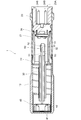
- FIG. 1 is an exploded perspective view of the sensor 1 according to the embodiment of the present invention.
- FIG. 2 is a cross-sectional view of line II-II in a state where the sensor 1 shown in FIG. 1 is assembled. As shown by the arrows in FIG. 1, the direction from the clamp 20 to the housing 10 is the front, and the direction from the housing 10 to the clamp 20 is the rear along the axial direction of the sensor 1.
- the sensor 1 is a proximity sensor capable of detecting that a detection target is approaching in a non-contact manner, and is a housing 10, a clamp 20, a connector 23, an O-ring 24, a hard board 30, a detection unit 40, and a flexible sensor.
- a substrate 50, a reinforcing plate 60, and the like are provided.
- the housing 10 is formed in a tubular shape, and electronic components such as a hard substrate 30 and a detection unit 40 are housed therein.
- the housing 10 has an opening on the rear side, and electronic components such as the hard substrate 30 and the detection unit 40 are inserted through the opening.
- the housing 10 may be made of metal, resin, or the like.
- the outer shape of the sensor 1 is cylindrical, but the outer circumference of the housing 10 or the clamp 20 may be a prismatic shape.
- the clamp 20 has an outer member 21 having a substantially cylindrical shape and an inner member 22 having a substantially cylindrical shape.
- the inner member 22 is fitted into the outer member 21 from the front side, and the end portion of the inner member 22 is connected to the opening of the housing 10. Further, the connector 23 is fitted into the inside of the outer member 21 from the rear side via the O-ring 24. A terminal provided at one end of the flexible substrate 50 is connected to the front end of the connector 23.
- the hard board 30 is a board on which a control circuit (not shown) for controlling the detection unit 40 and a current supply circuit (not shown) for supplying current to the detection unit 40 are mounted, and a part thereof is housed in the housing 10. ..
- a detection unit 40 is attached to the front end of the hard substrate 30.
- the hard substrate 30 for example, a rigid wiring board in which a glass-epoxy resin-based material is used as the base material is used.
- the detection unit 40 detects the presence or absence of a detection target in a non-contact manner.
- the detection unit 40 includes a core 41 in which the coil 42 is housed, and a coil 42 wound in an annular shape.
- terminals are provided at the rear end of the hard board 30, and the terminals are electrically connected to the terminals provided at one end of the flexible board 50.
- the exciting current is supplied to the coil 42 from the current supply circuit mounted on the hard board 30.
- the coil 42 generates a magnetic field based on the supplied exciting current.
- an eddy current is generated inside the detection target according to the law of electromagnetic induction. Since this eddy current generates a magnetic field, the magnetic flux penetrating the coil 42, and thus the impedance of the coil 42, changes.
- the control circuit connected to the detection unit 40 measures the change in the impedance of the coil 42 and detects the presence or absence of the detection target.
- the flexible substrate 50 has a third surface 51 and a fourth surface 52, and is curved in a substantially S shape in a cross-sectional view.
- the end of the flexible substrate 50 contacts the fourth surface 52 with the first surface 31 of the hard substrate 30 (when it is in direct contact, when it is in contact via a wiring layer or the like, or when it partially contains a gap, etc.) Is placed on the hard substrate 30 so as to be mounted on the hard substrate 30.
- the other end of the flexible substrate 50 is electrically connected to the connector 23.
- a wiring board in which a polyimide resin-based material, which is a heat-resistant resin, is used as the base material is used.
- the space provided with the flexible substrate 50 in the sensor 1 may be sealed with a predetermined resin.
- a reinforcing plate 60 is placed on the fourth surface 52 of the flexible substrate 50.
- the connector 23 may supply electric power from an external power source to the circuits mounted on the hard board 30 and the flexible board 50. Further, the connector 23 may transmit an output signal from the control circuit mounted on the hard board 30 and the flexible board 50 to an external device such as an amplifier.
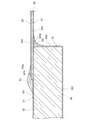
- FIG. 3 shows a portion where one end of the flexible substrate 50 is placed on one end of the hard substrate 30.
- the hard substrate 30 has a first surface 31, a second surface 32, and an end surface 33.
- the first surface 31 is arranged on the side facing the flexible substrate 50.
- the second surface 32 is arranged on the side that does not face the flexible substrate 50, that is, on the back side of the first surface 31.
- the end surface 33 is arranged so as to be continuous with the first surface 31 and the second surface 32 at the end of the hard substrate 30.
- a wiring layer W1 (first wiring layer W1) is provided on at least a part of the first surface 31 of the hard substrate 30.
- a terminal W1t which is a solder bonding region, is provided in a part of the wiring layer W1.
- the wiring layer W2 (second wiring layer W2) is provided over at least a part of the second surface 32 of the hard substrate 30 and at least a part of the end surface 33.
- a terminal W2t which is a solder joint region, is provided in a part of the wiring layer W2 arranged on the end surface 33.
- the wiring layers W1 and W2 and the like are formed, for example, by patterning copper attached to the main surface of the base material with an adhesive.
- the flexible substrate 50 has a third surface 51 and a fourth surface 52.
- the third surface 51 is arranged on the side facing the hard substrate 30.
- the fourth surface 52 is arranged on the side that does not face the hard substrate 30, that is, on the back side of the third surface 51.
- a wiring layer W3 (third wiring layer W3) is provided on at least a part of the third surface 51.
- a wiring layer W4 (fourth wiring layer W4) is provided on at least a part of the fourth surface 52.
- the wiring layers W3, W4, and the like are formed by, for example, tin-plating the surface of a copper foil attached to the main surface of a base material using an adhesive.
- the end of the third surface 51 of the flexible substrate 50 is arranged on at least a part of the first surface 31 of the hard substrate 30.
- the solder S1 extends over the terminal W1t of the wiring layer W1 provided on the first surface 31 of the hard substrate 30 and the terminal W4t of the wiring layer W4 provided on the fourth surface 52 of the flexible substrate 50. There is. As a result, the solder S1 electrically connects the terminal W1t and the terminal W4t.
- the solder S2 extends over the terminal W2t of the wiring layer W2 provided on the end surface 33 of the hard substrate 30 and the terminal W3t of the wiring layer W3 provided on the third surface 51 of the flexible substrate 50. As a result, the solder S2 electrically connects the terminal W2t and the terminal W3t.
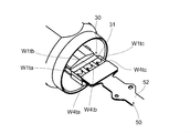
- FIG. 4A is a perspective view of the first surface 31 of the hard substrate 30 and the fourth surface 52 of the flexible substrate 50 as viewed obliquely.
- FIG. 4B is a perspective view of the second surface 32 of the hard substrate 30 and the third surface 51 of the flexible substrate 50 as viewed obliquely.
- the first surface 31 of the hard substrate 30 is provided with three terminals W1ta, W1tb, and W1tc of the wiring layer W1.
- the fourth surface 52 of the flexible substrate 50 is provided with three terminals W4ta, W4tb, and W4tc of the wiring layer W4. Then, as described with reference to FIG. 3, the terminal W1ta is electrically connected to the terminal W4ta, the terminal W1tb is electrically connected to the terminal W4tb, and the terminal W1tc is electrically connected to the terminal W4ct. That is, the wiring layer W1 of the hard board 30 and the wiring layer W4 of the flexible board 50 are electrically connected by three terminals.
- the second surface 32 of the hard substrate 30 is provided with four terminals W2ta, W2tb, W2tk, and W2td of the wiring layer W2.
- the third surface 51 of the flexible substrate 50 is provided with four terminals W3ta, W3tb, W3tc, and W3td of the wiring layer W3.
- the terminal W2ta is electrically connected to the terminal W3ta
- the terminal W2tb is electrically connected to the terminal W3tb
- the terminal W2tc is electrically connected to the terminal W3tc
- the terminal W2td is electrically connected to the terminal W3td. That is, the wiring layer W2 of the hard board 30 and the wiring layer W4 of the flexible board 50 are electrically connected by four terminals.
- the first surface 31 of the hard substrate 30 on which the solder S1 is provided and the fourth surface 52 of the flexible substrate 50 are arranged substantially parallel to each other.
- the end surface 33 of the hard substrate 30 on which the solder S2 is provided and the third surface 51 of the flexible substrate 50 are arranged substantially perpendicular to each other. Therefore, the solder S2 can suppress the spread of the solder S2 to be smaller than that of the solder S1.
- the number of terminals connected by the solder S2 (4) is larger than the number of terminals connected by the solder S1 (3). This makes it possible to connect the hard substrate 30 and the flexible substrate 50 with a small amount of solder.
- Each terminal W2ta, W2tb, W2tc, W2td, etc. of the wiring layer W2 provided on the end surface 33 of the hard substrate 30 forms a through hole with respect to the base material of the hard substrate 30, and the portion of the through hole. It may be produced by dividing the base material with.
- FIG. 5 is a cross-sectional view corresponding to FIG. 2 of the sensor 1'according to another embodiment of the present invention.
- the flexible substrate 50 is curved so as to apply a restoring force to the hard substrate 30. That is, the flexible substrate 50 has a curved portion in which the third surface 51 is arranged on the outside and the fourth surface 52 is arranged on the inside. As a result, the flexible substrate 50 exerts a restoring force that tries to restore the curvature of the curved portion. Then, the restoring force is applied from the third surface 51 of the flexible substrate 50 to the first surface 31 of the hard substrate 30 facing the third surface 51. As a result, the connection between the hard substrate 30 and the flexible substrate 50 becomes stronger.
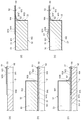
- FIG. 6 is a diagram for explaining a method of connecting the hard substrate 30 and the flexible substrate 50 according to the embodiment of the present invention.
- FIG. 3 is drawn to explain the connection structure of the hard substrate 30 and the flexible substrate 50 according to the embodiment of the present invention, and is in the state of FIG. 3 in the following procedures (1) to (4). It should be noted that the top and bottom are turned inside out.
- the flexible substrate 50 is placed on a flat base D with the third surface 51 facing upward.
- the hard substrate 30 is placed on the flexible substrate 50 with the first surface 31 facing downward so as to face the flexible substrate 50.
- the terminal W2t of the wiring layer W2 provided on the end surface 33 of the hard substrate 30 and the terminal of the wiring layer W3 provided on the third surface 51 of the flexible substrate 50 is adjusted so that the W3t and the W3t have a solderable positional relationship.
- the solder S2 is formed so as to cover the terminal W3t, and the terminal W2t and the terminal W3t are electrically connected by the solder S2.
- soldering it is desirable to press the hard substrate 30 downward to bring the wiring layer W2 and the wiring layer W3 into close contact with each other.
- solder so as to cover the terminal W1t of the wiring layer W1 provided on the first surface 31 of the hard board 30 and the terminal W4t of the wiring layer W4 provided on the fourth surface 52 of the flexible board 50. S1 is formed, and these terminals W1t and terminals W4t are electrically connected by solder S1.
- the terminals W2t of the wiring layer W2 provided on the end surface 33 of the hard substrate 30 and the third surface 51 of the flexible substrate 50 are formed. It is possible to perform soldering in a state where the terminal W3t of the provided wiring layer W3 is in close contact with the terminal W3t. As a result, the terminal W2t of the wiring layer W2 provided on the end surface 33 of the hard substrate 30 and the terminal W3t of the wiring layer W3 provided on the third surface 51 of the flexible substrate 50 can be easily and accurately soldered. And the electrical connection of these terminals can be made reliably.
- the number of terminals connected by the solder S2 is larger than the number of terminals connected by the solder S1. Therefore, the terminals W2ta, W2tb, W2tc, and W2td of the wiring layer W2 connected by the solder S2 are 3 of the wiring layer W1 provided on the first surface 31 of the hard substrate 30 connected by the solder S1. The area is smaller than that of the two terminals W1ta, W1tb, and W1tc. The smaller the area of the terminals, the more precise the alignment of the terminals to be connected by soldering is required.
- solder S2 which is more difficult to align, before the solder S1 by the procedure described above, it is possible to reduce the misalignment between the terminals of the hard board 30 and the flexible board 50, and the hard board 30 can be reduced. And the flexible substrate 50 can be reliably electrically connected.
- 1, 1'... sensor, 10 ... housing, 20 ... clamp, 21 ... outer member, 22 ... inner member, 23 ... connector, 24 ... O-ring, 30 ... hard board, 31 ... first surface, 32 ... second Surface, 33 ... End surface, 40 ... Detection unit, 41 ... Core, 42 ... Coil, 50 ... Flexible substrate, 51 ... Third surface, 52 ... Fourth surface, 60 ... Reinforcing plate
Landscapes
- Engineering & Computer Science (AREA)
- Microelectronics & Electronic Packaging (AREA)
- Manufacturing & Machinery (AREA)
- Combinations Of Printed Boards (AREA)
- Printing Elements For Providing Electric Connections Between Printed Circuits (AREA)
- Switches That Are Operated By Magnetic Or Electric Fields (AREA)
Abstract
ハード基板の部品実装スペースを確保しつつ全体を小型化することの可能な電子機器及び近接センサを提供する。本発明の一態様に係る電子機器は、第1配線層の端子が設けられた第1面と、第1面の裏側に位置する第2面と、第2配線層の端子が設けられ且つ第1面及び第2面に連続する端面と、を有するハード基板と、第3配線層の端子が設けられ且つハード基板の第1面に対向する第3面と、第4配線層の端子が設けられ且つ第3面の裏側に位置する第4面と、を有するフレキシブル基板と、を備え、ハード基板の第1面に設けられた第1配線層の端子と、フレキシブル基板の第4面に設けられた第4配線層の端子とは、半田によって電気的に接続されており、ハード基板の端面に設けられた第2配線層の端子と、フレキシブル基板の第3面に設けられた第3配線層の端子とは、半田によって電気的に接続されている。
Description
本発明は、電子機器及び近接センサに関する。
従来から、電子機器において、ハード基板に設けられた配線層とフレキシブル基板に設けられた配線層とを接続することが行われている。例えば、特許文献1には、フレキシブル配線基板の接続方法が記載されている。
しかしながら、配線層同士の接続点数が増えるにつれて、ハード基板の表面における半田付けに必要なスペースも増大するため、電子機器の小型化が困難になる。
そこで、本発明は、ハード基板の部品実装スペースを確保しつつ全体を小型化することの可能な電子機器及び近接センサを提供することを目的とする。
本発明の一態様に係る電子機器は、第1配線層の端子が設けられた第1面と、第1面の裏側に位置する第2面と、第2配線層の端子が設けられ且つ第1面及び第2面に連続する端面と、を有するハード基板と、第3配線層の端子が設けられ且つハード基板の第1面に対向する第3面と、第4配線層の端子が設けられ且つ第3面の裏側に位置する第4面と、を有するフレキシブル基板と、を備え、ハード基板の第1面に設けられた第1配線層の端子と、フレキシブル基板の第4面に設けられた第4配線層の端子とは、半田によって電気的に接続されており、ハード基板の端面に設けられた第2配線層の端子と、フレキシブル基板の第3面に設けられた第3配線層の端子とは、半田によって電気的に接続されている。
この態様によれば、電子機器について、ハード基板の部品実装スペースを確保しつつ全体を小型化することが可能となる。
上記態様において、フレキシブル基板は、第3面がハード基板の第1面に対して復元力を加えるように湾曲していてもよい。
この態様によれば、フレキシブル基板が第3面を介してハード基板の第1面に対して復元力を加えるように固定されるため、フレキシブル基板の第3面がハード基板の第1面に対してより強固に固定される。
上記態様において、フレキシブル基板は、第3面が外側に配置され且つ第4面が内側に配置される湾曲部を有してもよい。
この態様によれば、フレキシブル基板が第3面を介してハード基板の第1面に対して復元力を加えるように固定されるため、フレキシブル基板の第3面がハード基板の第1面に対してより強固に固定される。
上記態様において、第2配線層の端子は、端面が有する凹部に設けられてもよい。
この態様によれば、例えば基材にスルーホールを施した上で、該スルーホールで基材を分割することにより、ハード基板を製造することが可能となり、電子機器の製造方法を簡素化することが可能となる。
上記態様において、凹部は、第1面及び第2面に略垂直な方向を軸方向とする略円筒形状の面を構成してもよい。
この態様によれば、例えば基材にスルーホールを施した上で、該スルーホールで基材を分割することにより、ハード基板を製造することが可能となり、電子機器の製造方法を簡素化することが可能となる。
上記態様において、第2配線層は、ハード基板の第2面の上及び/又はハード基板の内部に設けられてもよい。
この態様によれば、第2配線層をハード基板の表面及び/又は内部に設けることができ、配線の自由度が増加する。
上記態様において、互いに電気的に接続される第2配線層の端子及び第3配線層の数は、互いに電気的に接続される第1配線層の端子及び第4配線層の端子の数よりも多くてもよい。
この態様によれば、少ない量の半田でハード基板30及びフレキシブル基板50を接続することが可能となる。
本発明によれば、部品点数を抑え、配線層の接続のためのスペースを小さくすることの可能な電子機器及び近接センサを提供することができる。
添付図面を参照して、本発明の実施形態について説明する。なお、各図において、同一の符号を付したものは、同一又は同様の構成を有する。
図1及び図2を参照して、センサ1の内部構造について説明する。図1は、本発明の実施形態に係るセンサ1の分解斜視図である。図2は、図1に示すセンサ1を組み立てた状態におけるII-II線の断面図である。図1の矢印で示すように、センサ1の軸方向に沿って、クランプ20から筐体10に向かう方向を前方とし、筐体10からクランプ20に向かう方向を後方とする。
本実施形態に係るセンサ1は、非接触で検出対象が近づいたことを検出可能な近接センサであり、筐体10、クランプ20、コネクタ23、Oリング24、ハード基板30、検出部40、フレキシブル基板50、及び補強板60等を備える。筐体10は、筒形状に形成されており、内部にハード基板30及び検出部40等の電子部品が収容される。筐体10は、後方側に開口部を有しており、当該開口部からハード基板30及び検出部40等の電子部品が挿入される。筐体10は、金属や樹脂等で形成されてもよい。センサ1は、その外形が円柱形状となっているが、筐体10やクランプ20の外周が多角形である角柱形状であってもよい。
クランプ20は、略円筒形状を呈した外側部材21と、略円筒形状を呈した内側部材22とを有する。外側部材21の内部には、前方側から内側部材22が嵌め込まれた上で、内側部材22の端部が筐体10の開口部に接続される。また、外側部材21の内部には、後方側から、Oリング24を介してコネクタ23が嵌め込まれる。コネクタ23の前方側の端部には、フレキシブル基板50の一端に設けられた端子が接続される。
ハード基板30は、検出部40を制御する制御回路(不図示)及び検出部40に電流を供給する電流供給回路(不図示)を搭載する基板であり、筐体10に一部が収容される。ハード基板30の前方側の端部には、図2に示すように検出部40が取り付けられている。ハード基板30は、たとえば基材にガラス-エポキシ樹脂系の材料が利用されたリジッド配線基板が利用される。検出部40は、検出対象の有無を非接触で検出する。検出部40は、コイル42が収容されるコア41と、環状に巻かれたコイル42とを備える。一方、後述するように、ハード基板30の後方側の端部には端子が設けられており、当該端子がフレキシブル基板50の一端に設けられた端子と電気的に接続される。
センサ1による検出対象の検出方法を説明する。まず、ハード基板30に搭載された電流供給回路からコイル42に励磁電流が供給される。コイル42は、供給された励磁電流に基づいて磁場を発生させる。この状態でコイル42に金属等の検出対象が接近すると、電磁誘導の法則により検出対象内部に渦電流が発生する。この渦電流は磁場を発生させるため、コイル42を貫く磁束、ひいてはコイル42のインピーダンスが変化する。検出部40に接続された制御回路は、コイル42のインピーダンスの変化を測定し、検出対象の有無を検出する。
図2に示すとおり、フレキシブル基板50は、第3面51及び第4面52を有しており、断面図視において略S字上に湾曲している。フレキシブル基板50の端部は、第4面52をハード基板30の第1面31に接触(直接接触する場合の他、配線層等を介して接触する場合や、一部に空隙を含む場合等を含む)させるようにして、ハード基板30に載置される。フレキシブル基板50の他端は、コネクタ23に電気的に接続される。フレキシブル基板50としては、たとえば基材に耐熱性樹脂であるポリイミド樹脂系の材料が利用された配線基板が利用される。センサ1におけるフレキシブル基板50が設けられた空間は、所定の樹脂により封止されてもよい。フレキシブル基板50の第4面52の上には、補強板60が載置される。フレキシブル基板50が歪曲すると、半田付け部分に応力が生じて当該部分も歪曲しようとするが、当該補強板60により半田付け部分の歪曲を抑えることが可能となる。
コネクタ23は、外部電源からの電力をハード基板30及びフレキシブル基板50に搭載された回路へ供給してもよい。また、コネクタ23は、ハード基板30及びフレキシブル基板50に搭載された制御回路からの出力信号をアンプ等の外部機器へ伝達してもよい。
次に、図3を参照して、ハード基板30及びフレキシブル基板50の接続構造について説明する。図3には、フレキシブル基板50の一端がハード基板30の一端に載置される部分が示されている。図3に示すとおり、ハード基板30は、第1面31と、第2面32と、端面33とを有する。第1面31は、フレキシブル基板50に対向する側に配置される。第2面32は、フレキシブル基板50に対向しない側、すなわち第1面31の裏側に配置される。端面33は、ハード基板30の端部において第1面31及び第2面32に連続するように配置される。
ハード基板30の第1面31の少なくとも一部には、配線層W1(第1配線層W1)が設けられる。配線層W1の一部には、半田接合領域である端子W1tが設けられている。ハード基板30の第2面32の少なくとも一部及び端面33の少なくとも一部に渡って、配線層W2(第2配線層W2)が設けられる。配線層W2の端面33上に配置される一部には、半田接合領域である端子W2tが設けられている。配線層W1及びW2等は、たとえば基材の主表面に接着剤にて貼り付けられた銅をパターニングすること等によって形成される。
フレキシブル基板50は、第3面51と、第4面52とを有する。第3面51は、ハード基板30に対向する側に配置される。第4面52は、ハード基板30に対向しない側、すなわち第3面51の裏側に配置される。第3面51の少なくとも一部には、配線層W3(第3配線層W3)が設けられる。第4面52の少なくとも一部には、配線層W4(第4配線層W4)が設けられる。配線層W3及びW4等は、たとえば接着剤を用いて基材の主表面に貼り付けられた銅箔の表面にスズめっきが施されること等によって形成される。
フレキシブル基板50の第3面51の端部は、ハード基板30の第1面31の少なくとも一部の上に配置される。ハード基板30の第1面31に設けられた配線層W1の端子W1tと、フレキシブル基板50の第4面52に設けられた配線層W4の端子W4tとに渡って、半田S1が延在している。これにより、半田S1は、端子W1tと、端子W4tとを、電気的に接続している。
ハード基板30の端面33に設けられた配線層W2の端子W2tと、フレキシブル基板50の第3面51に設けられた配線層W3の端子W3tとに渡って、半田S2が延在している。これにより、半田S2は、端子W2tと、端子W3tとを、電気的に接続している。
次に、図4A及び図4Bを参照して、ハード基板30及びフレキシブル基板50の接続構造における端子の数について説明する。図4Aは、ハード基板30の第1面31及びフレキシブル基板50の第4面52を斜めからみた斜視図である。図4Bは、ハード基板30の第2面32及びフレキシブル基板50の第3面51を斜めからみた斜視図である。
図4Aに示すとおり、ハード基板30の第1面31には、配線層W1の3つの端子W1ta、W1tb、及びW1tcが設けられている。また、フレキシブル基板50の第4面52には、配線層W4の3つの端子W4ta、W4tb、及びW4tcが設けられている。そして、図3を用いて説明したように、端子W1taは端子W4taと、端子W1tbは端子W4tbと、端子W1tcは端子W4tcと、それぞれ電気的に接続される。すなわち、ハード基板30の配線層W1と、フレキシブル基板50の配線層W4とは、3つの端子によって電気的に接続される。
図4Bに示すとおり、ハード基板30の第2面32には、配線層W2の4つの端子W2ta、W2tb、W2tc、及びW2tdが設けられている。また、フレキシブル基板50の第3面51には、配線層W3の4つの端子W3ta、W3tb、W3tc、及びW3tdが設けられている。そして、図3を用いて説明したように、端子W2taは端子W3taと、端子W2tbは端子W3tbと、端子W2tcは端子W3tcと、端子W2tdは端子W3tdと、それぞれ電気的に接続される。すなわち、ハード基板30の配線層W2と、フレキシブル基板50の配線層W4とは、4つの端子によって電気的に接続される。
半田S1が設けられるハード基板30の第1面31及びフレキシブル基板50の第4面52は、互いに略平行に配置される。一方、半田S2が設けられるハード基板30の端面33及びフレキシブル基板50の第3面51は、互いに略垂直に配置される。そのため、半田S2は、半田S1と比較して、広がりを小さく抑えることが可能となる。そして、上述したとおり、半田S2により接続される端子の数(4つ)は、半田S1により接続される端子の数(3つ)よりも多い。これにより、少ない量の半田でハード基板30及びフレキシブル基板50を接続することが可能となる。
なお、ハード基板30の端面33に設けられる配線層W2の各端子W2ta、W2tb、W2tc、及びW2td等は、例えば、ハード基板30の基材に対してスルーホールを形成し、当該スルーホールの部分で基材を分割等することによって生成されてもよい。
図5は、本発明の他の実施形態に係るセンサ1’の図2に相当する断面図である。センサ1’では、フレキシブル基板50がハード基板30に復元力を加えるように湾曲する。すなわち、フレキシブル基板50は、第3面51が外側に配置され、第4面52が内側に配置される湾曲部を有する。これにより、フレキシブル基板50には、当該湾曲部の湾曲を元に戻そうとする復元力がはたらく。そして、フレキシブル基板50の第3面51から、当該第3面51に対向するハード基板30の第1面31に対して、当該復元力が加えられる。これにより、ハード基板30及びフレキシブル基板50の接続がより強固になる。
図6は、本発明の実施形態に係るハード基板30及びフレキシブル基板50の接続方法を説明するための図である。なお、図3は、本発明の実施形態に係るハード基板30及びフレキシブル基板50の接続構造を説明するために描かれたものであり、下記手順(1)~(4)においては図3の状態に対して上下が裏返しの状態となることに注意が必要である。
(1)まず、図6(a)に示すように、フレキシブル基板50を、第3面51が上を向いた状態で平らな台Dの上に載置する。
(2)次に、図6(b)に示すように、ハード基板30を、第1面31がフレキシブル基板50と対向するように下を向いた状態で、フレキシブル基板50上に載置する。
(3)更に、図6(b)に示すように、ハード基板30の端面33に設けられた配線層W2の端子W2tと、フレキシブル基板50の第3面51に設けられた配線層W3の端子W3tとが半田付け可能な位置関係になるよう、ハード基板30の位置を調整する。
(4)次に、図6(c)に示すように、ハード基板30の端面33に設けられた配線層W2の端子W2tと、フレキシブル基板50の第3面51に設けられた配線層W3の端子W3tとを覆うように半田S2を形成し、これら端子W2tと端子W3tとを半田S2により電気的に接続する。半田付けを行う際にはハード基板30を下向きに押圧して配線層W2と配線層W3を密着させることが望ましい。
(5)次に、ハード基板30の第1面31が上を向くように、配線層W2の端子W2tと配線層W3の端子W3tとが半田S2で接続されたハード基板30とフレキシブル基板50とを、上下裏返す。
(6)次に、ハード基板30の第1面31に設けられた配線層W1の端子W1tと、フレキシブル基板50の第4面52に設けられた配線層W4の端子W4tとを覆うように半田S1を形成し、これら端子W1tと端子W4tとを半田S1により電気的に接続する。
(2)次に、図6(b)に示すように、ハード基板30を、第1面31がフレキシブル基板50と対向するように下を向いた状態で、フレキシブル基板50上に載置する。
(3)更に、図6(b)に示すように、ハード基板30の端面33に設けられた配線層W2の端子W2tと、フレキシブル基板50の第3面51に設けられた配線層W3の端子W3tとが半田付け可能な位置関係になるよう、ハード基板30の位置を調整する。
(4)次に、図6(c)に示すように、ハード基板30の端面33に設けられた配線層W2の端子W2tと、フレキシブル基板50の第3面51に設けられた配線層W3の端子W3tとを覆うように半田S2を形成し、これら端子W2tと端子W3tとを半田S2により電気的に接続する。半田付けを行う際にはハード基板30を下向きに押圧して配線層W2と配線層W3を密着させることが望ましい。
(5)次に、ハード基板30の第1面31が上を向くように、配線層W2の端子W2tと配線層W3の端子W3tとが半田S2で接続されたハード基板30とフレキシブル基板50とを、上下裏返す。
(6)次に、ハード基板30の第1面31に設けられた配線層W1の端子W1tと、フレキシブル基板50の第4面52に設けられた配線層W4の端子W4tとを覆うように半田S1を形成し、これら端子W1tと端子W4tとを半田S1により電気的に接続する。
このような手順を用いてハード基板30及びフレキシブル基板50の接続構造を形成することにより、ハード基板30の端面33に設けられた配線層W2の端子W2tと、フレキシブル基板50の第3面51に設けられた配線層W3の端子W3tとが密着した状態で半田付けを行うことが可能となる。これにより、ハード基板30の端面33に設けられた配線層W2の端子W2tと、フレキシブル基板50の第3面51に設けられた配線層W3の端子W3tとの半田付けを容易且つ正確に行うことができ、これら端子の電気的接続を確実に行うことができる。
また、図4A、図4Bに示すとおり、半田S2で接続される端子の数は半田S1で接続される端子の数よりも多い。このため、半田S2で接続される、配線層W2の各端子W2ta、W2tb、W2tc、及びW2tdは、半田S1で接続される、ハード基板30の第1面31に設けられた配線層W1の3つの端子W1ta、W1tb、及びW1tcに比べて面積が小さくなる。端子の面積が小さい程、半田で接続しようとする端子同士の位置合わせにおいてより精密さが要求される。したがって、上述した手順により、位置合わせがより困難な半田S2を半田S1よりも先に形成することにより、ハード基板30及びフレキシブル基板50の端子同士の位置ずれを少なくすることができ、ハード基板30及びフレキシブル基板50の電気的接続を確実に行うことができる。
以上説明した実施形態は、本発明の理解を容易にするためのものであり、本発明を限定して解釈するためのものではない。実施形態が備える各要素並びにその配置、材料、条件、形状及びサイズ等は、例示したものに限定されるわけではなく適宜変更することができる。また、異なる実施形態で示した構成同士を部分的に置換し又は組み合わせることが可能である。
1、1’…センサ、10…筐体、20…クランプ、21…外側部材、22…内側部材、23…コネクタ、24…Oリング、30…ハード基板、31…第1面、32…第2面、33…端面、40…検出部、41…コア、42…コイル、50…フレキシブル基板、51…第3面、52…第4面、60…補強板
Claims (9)
- 第1配線層の端子が設けられた第1面と、前記第1面の裏側に位置する第2面と、第2配線層の端子が設けられ且つ前記第1面及び前記第2面に連続する端面と、を有するハード基板と、
第3配線層の端子が設けられ且つ前記ハード基板の前記第1面に対向する第3面と、第4配線層の端子が設けられ且つ前記第3面の裏側に位置する第4面と、を有するフレキシブル基板と、を備え、
前記ハード基板の前記第1面に設けられた前記第1配線層の端子と、前記フレキシブル基板の前記第4面に設けられた前記第4配線層の端子とは、半田によって電気的に接続されており、
前記ハード基板の前記端面に設けられた前記第2配線層の端子と、前記フレキシブル基板の前記第3面に設けられた前記第3配線層の端子とは、半田によって電気的に接続されている、電子機器。 - 前記フレキシブル基板は、前記第3面が前記ハード基板の前記第1面に対して復元力を加えるように湾曲している、請求項1に記載の電子機器。
- 前記フレキシブル基板は、前記第3面が外側に配置され且つ前記第4面が内側に配置される湾曲部を有する、請求項2に記載の電子機器。
- 前記第2配線層の端子は、前記端面が有する凹部に設けられる、請求項1から3のいずれか一項に記載の電子機器。
- 前記凹部は、前記第1面及び前記第2面に略垂直な方向を軸方向とする略円筒形状の面を構成する、請求項4に記載の電子機器。
- 前記第2配線層は、前記ハード基板の前記第2面の上及び/又は前記ハード基板の内部に設けられる、請求項1から5のいずれか一項に記載の電子機器。
- 互いに電気的に接続される前記第2配線層の端子及び前記第3配線層の端子の数は、互いに電気的に接続される前記第1配線層の端子及び前記第4配線層の端子の数よりも多い、請求項1から6のいずれか一項に記載の電子機器。
- 筐体と、
前記筐体の内部に配置された請求項1から7のいずれか一項に記載の電子機器と、
前記ハード基板に接続された検出部と、を備える、近接センサ。 - 第1配線層の端子が設けられた第1面と、前記第1面の裏側に位置する第2面と、第2配線層の端子が設けられ且つ前記第1面及び前記第2面に連続する端面と、を有するハード基板と、
第3配線層の端子が設けられ且つ前記ハード基板の前記第1面に対向する第3面と、第4配線層の端子が設けられ且つ前記第3面の裏側に位置する第4面と、を有するフレキシブル基板と、を接続する方法であって、
前記ハード基板の前記端面に設けられた前記第2配線層の端子と、前記フレキシブル基板の前記第3面に設けられた前記第3配線層の端子とを、半田によって電気的に接続するステップと、
前記ハード基板の前記第1面に設けられた前記第1配線層の端子と、前記フレキシブル基板の前記第4面に設けられた前記第4配線層の端子とを、半田によって電気的に接続するステップと、を含む方法。
Priority Applications (4)
| Application Number | Priority Date | Filing Date | Title |
|---|---|---|---|
| CN202180012053.3A CN115039519A (zh) | 2020-03-10 | 2021-01-20 | 电子设备及接近传感器 |
| DE112021000339.9T DE112021000339T5 (de) | 2020-03-10 | 2021-01-20 | Elektronisches Gerät und Näherungssensor |
| US17/798,086 US12075567B2 (en) | 2020-03-10 | 2021-01-20 | Electronic apparatus and proximity sensor |
| KR1020227026920A KR102694954B1 (ko) | 2020-03-10 | 2021-01-20 | 전자 기기 및 근접 센서 |
Applications Claiming Priority (2)
| Application Number | Priority Date | Filing Date | Title |
|---|---|---|---|
| JP2020040797A JP7508035B2 (ja) | 2020-03-10 | 2020-03-10 | 電子機器及び近接センサ |
| JP2020-040797 | 2020-03-10 |
Publications (1)
| Publication Number | Publication Date |
|---|---|
| WO2021181898A1 true WO2021181898A1 (ja) | 2021-09-16 |
Family
ID=77671303
Family Applications (1)
| Application Number | Title | Priority Date | Filing Date |
|---|---|---|---|
| PCT/JP2021/001782 Ceased WO2021181898A1 (ja) | 2020-03-10 | 2021-01-20 | 電子機器及び近接センサ |
Country Status (6)
| Country | Link |
|---|---|
| US (1) | US12075567B2 (ja) |
| JP (1) | JP7508035B2 (ja) |
| KR (1) | KR102694954B1 (ja) |
| CN (1) | CN115039519A (ja) |
| DE (1) | DE112021000339T5 (ja) |
| WO (1) | WO2021181898A1 (ja) |
Citations (3)
| Publication number | Priority date | Publication date | Assignee | Title |
|---|---|---|---|---|
| JPH06152092A (ja) * | 1992-11-10 | 1994-05-31 | Murata Mfg Co Ltd | 表面実装型基板アセンブリ |
| JP2003518394A (ja) * | 1999-07-02 | 2003-06-10 | プロソニック カンパニー リミテッド | 線型あるいは曲線型の超音波変換器とその接続技術 |
| JP2006236948A (ja) * | 2005-02-28 | 2006-09-07 | Omron Corp | 近接センサおよびその製造方法 |
Family Cites Families (21)
| Publication number | Priority date | Publication date | Assignee | Title |
|---|---|---|---|---|
| JPS55124296A (en) * | 1979-03-19 | 1980-09-25 | Matsushita Electric Industrial Co Ltd | Soldering method |
| JPS58134844A (ja) | 1982-01-25 | 1983-08-11 | 安川設備技研株式会社 | パルプ解梱方法とその装置 |
| JPS58134844U (ja) * | 1982-03-05 | 1983-09-10 | オムロン株式会社 | 検出器 |
| DE3414480C2 (de) * | 1984-04-17 | 1993-02-25 | Ifm Electronic Gmbh, 4300 Essen | Elektrisches, insbesondere elektronisches, berührungslos arbeitendes Schaltgerät |
| US6292370B1 (en) * | 1999-10-01 | 2001-09-18 | Motorola, Inc. | Flexible circuit board and method for making a flexible circuit board |
| JP4667652B2 (ja) * | 2001-06-12 | 2011-04-13 | ローム株式会社 | 電池パック、およびその製造方法 |
| JP2004031870A (ja) * | 2002-06-28 | 2004-01-29 | Omron Corp | リジッド基板およびフレキシブル基板のはんだ付け接合方法 |
| US7304373B2 (en) * | 2004-10-28 | 2007-12-04 | Intel Corporation | Power distribution within a folded flex package method and apparatus |
| JP2006245108A (ja) | 2005-03-01 | 2006-09-14 | Omron Corp | フレキシブル配線基板の接続方法および接続構造 |
| JP4777759B2 (ja) * | 2005-12-01 | 2011-09-21 | 富士フイルム株式会社 | 配線基板及び配線基板接続装置 |
| KR100659826B1 (ko) * | 2005-12-20 | 2006-12-19 | 삼성에스디아이 주식회사 | 배터리 팩의 회로 기판 |
| WO2007084552A2 (en) * | 2006-01-17 | 2007-07-26 | Lifesync Corporation | Multi-lead keyhold connector |
| JP4934325B2 (ja) * | 2006-02-17 | 2012-05-16 | 株式会社フジクラ | プリント配線板の接続構造及びプリント配線板の接続方法 |
| JP2008108909A (ja) * | 2006-10-25 | 2008-05-08 | Sharp Corp | フレキシブル配線基板の接続構造、および、電子機器 |
| JP2010087427A (ja) * | 2008-10-02 | 2010-04-15 | Sumitomo Electric Ind Ltd | 回路部材の接続構造 |
| TWI425298B (zh) * | 2010-05-21 | 2014-02-01 | Delta Electronics Inc | 可撓性連接之數位微鏡模組及其適用之投影裝置 |
| TWM450838U (zh) * | 2012-10-22 | 2013-04-11 | Bing Xu Prec Co Ltd | 軟性排線電連接器固定結構 |
| US9425527B2 (en) * | 2013-07-01 | 2016-08-23 | Sumitomo Electric Industries, Ltd. | Different-pitch flat cable connection structure, pitch-conversion flat cable, and method for producing pitch-conversion flat cable |
| EP3051635B1 (en) * | 2015-01-30 | 2018-01-17 | TE Connectivity Germany GmbH | Electric contact means and electrical cable assembly for the automotive industry |
| US20190150711A1 (en) * | 2017-11-17 | 2019-05-23 | ISSA Technology Co., Ltd. | Endoscope Apparatus |
| CN110248500B (zh) * | 2019-06-24 | 2021-05-04 | 深圳华麟电路技术有限公司 | 用于伸缩式摄像头的软硬结合板及其制作工艺 |
-
2020
- 2020-03-10 JP JP2020040797A patent/JP7508035B2/ja active Active
-
2021
- 2021-01-20 CN CN202180012053.3A patent/CN115039519A/zh active Pending
- 2021-01-20 WO PCT/JP2021/001782 patent/WO2021181898A1/ja not_active Ceased
- 2021-01-20 KR KR1020227026920A patent/KR102694954B1/ko active Active
- 2021-01-20 US US17/798,086 patent/US12075567B2/en active Active
- 2021-01-20 DE DE112021000339.9T patent/DE112021000339T5/de active Pending
Patent Citations (3)
| Publication number | Priority date | Publication date | Assignee | Title |
|---|---|---|---|---|
| JPH06152092A (ja) * | 1992-11-10 | 1994-05-31 | Murata Mfg Co Ltd | 表面実装型基板アセンブリ |
| JP2003518394A (ja) * | 1999-07-02 | 2003-06-10 | プロソニック カンパニー リミテッド | 線型あるいは曲線型の超音波変換器とその接続技術 |
| JP2006236948A (ja) * | 2005-02-28 | 2006-09-07 | Omron Corp | 近接センサおよびその製造方法 |
Also Published As
| Publication number | Publication date |
|---|---|
| KR102694954B1 (ko) | 2024-08-13 |
| JP2021144976A (ja) | 2021-09-24 |
| KR20220123690A (ko) | 2022-09-08 |
| US12075567B2 (en) | 2024-08-27 |
| JP7508035B2 (ja) | 2024-07-01 |
| DE112021000339T5 (de) | 2022-09-22 |
| CN115039519A (zh) | 2022-09-09 |
| US20230094727A1 (en) | 2023-03-30 |
Similar Documents
| Publication | Publication Date | Title |
|---|---|---|
| JP5970719B2 (ja) | 回路基板 | |
| EP1765035B1 (en) | Condenser microphone and packaging method for the same | |
| CN1933680B (zh) | 电容传声器及其封装方法 | |
| US8031127B2 (en) | Semiconductor memory module incorporating antenna | |
| US20070041597A1 (en) | Silicon based condenser microphone and packaging method for the same | |
| JP2003153392A (ja) | エレクトレットコンデンサマイクロホン | |
| JPH06123604A (ja) | 曲げセンサ | |
| JP7508035B2 (ja) | 電子機器及び近接センサ | |
| US20070215378A1 (en) | Circuit board | |
| CN115589521A (zh) | 摄像头模组及电子设备 | |
| JP3540361B2 (ja) | アンテナモジュールおよびその製造方法 | |
| WO2021220631A1 (ja) | 電子機器 | |
| US20110080245A1 (en) | Multilayer circuit board | |
| JP2018206996A (ja) | プリント基板の回路構造及びプリント基板 | |
| JP6460280B2 (ja) | 部品実装基板 | |
| CN119485895B (zh) | 电路板及其制造方法 | |
| US12230432B2 (en) | Circuit carrier for an electronic circuit, and method for producing the circuit carrier | |
| JP2007266481A (ja) | 多層基板 | |
| JP4900567B2 (ja) | モータドライブ装置の出力構造 | |
| JPH10256059A (ja) | 回路基板にコイルの磁路を設けた回路 | |
| KR20250106181A (ko) | Fpcb 어셈블리 및 이를 포함하는 전자 장치 | |
| JP2021182527A (ja) | 電子装置 | |
| JP2024044459A (ja) | 多層基板及び電子機器 | |
| JP2001313488A (ja) | シールド基板、シールド基板の実装方法及びシールド基板を用いた電子機器 | |
| JP2018014587A (ja) | 複合部品の調整方法 |
Legal Events
| Date | Code | Title | Description |
|---|---|---|---|
| 121 | Ep: the epo has been informed by wipo that ep was designated in this application |
Ref document number: 21767067 Country of ref document: EP Kind code of ref document: A1 |
|
| ENP | Entry into the national phase |
Ref document number: 20227026920 Country of ref document: KR Kind code of ref document: A |
|
| 122 | Ep: pct application non-entry in european phase |
Ref document number: 21767067 Country of ref document: EP Kind code of ref document: A1 |