WO2021161964A1 - 導電性接着剤組成物、及び、撮像モジュールを製造する方法 - Google Patents
導電性接着剤組成物、及び、撮像モジュールを製造する方法 Download PDFInfo
- Publication number
- WO2021161964A1 WO2021161964A1 PCT/JP2021/004618 JP2021004618W WO2021161964A1 WO 2021161964 A1 WO2021161964 A1 WO 2021161964A1 JP 2021004618 W JP2021004618 W JP 2021004618W WO 2021161964 A1 WO2021161964 A1 WO 2021161964A1
- Authority
- WO
- WIPO (PCT)
- Prior art keywords
- adhesive composition
- conductive adhesive
- conductive
- wiring board
- composition according
- Prior art date
- Legal status (The legal status is an assumption and is not a legal conclusion. Google has not performed a legal analysis and makes no representation as to the accuracy of the status listed.)
- Ceased
Links
Images



Classifications
-
- C—CHEMISTRY; METALLURGY
- C09—DYES; PAINTS; POLISHES; NATURAL RESINS; ADHESIVES; COMPOSITIONS NOT OTHERWISE PROVIDED FOR; APPLICATIONS OF MATERIALS NOT OTHERWISE PROVIDED FOR
- C09J—ADHESIVES; NON-MECHANICAL ASPECTS OF ADHESIVE PROCESSES IN GENERAL; ADHESIVE PROCESSES NOT PROVIDED FOR ELSEWHERE; USE OF MATERIALS AS ADHESIVES
- C09J11/00—Features of adhesives not provided for in group C09J9/00, e.g. additives
- C09J11/02—Non-macromolecular additives
- C09J11/04—Non-macromolecular additives inorganic
-
- C—CHEMISTRY; METALLURGY
- C09—DYES; PAINTS; POLISHES; NATURAL RESINS; ADHESIVES; COMPOSITIONS NOT OTHERWISE PROVIDED FOR; APPLICATIONS OF MATERIALS NOT OTHERWISE PROVIDED FOR
- C09J—ADHESIVES; NON-MECHANICAL ASPECTS OF ADHESIVE PROCESSES IN GENERAL; ADHESIVE PROCESSES NOT PROVIDED FOR ELSEWHERE; USE OF MATERIALS AS ADHESIVES
- C09J11/00—Features of adhesives not provided for in group C09J9/00, e.g. additives
- C09J11/02—Non-macromolecular additives
- C09J11/06—Non-macromolecular additives organic
-
- C—CHEMISTRY; METALLURGY
- C09—DYES; PAINTS; POLISHES; NATURAL RESINS; ADHESIVES; COMPOSITIONS NOT OTHERWISE PROVIDED FOR; APPLICATIONS OF MATERIALS NOT OTHERWISE PROVIDED FOR
- C09J—ADHESIVES; NON-MECHANICAL ASPECTS OF ADHESIVE PROCESSES IN GENERAL; ADHESIVE PROCESSES NOT PROVIDED FOR ELSEWHERE; USE OF MATERIALS AS ADHESIVES
- C09J163/00—Adhesives based on epoxy resins; Adhesives based on derivatives of epoxy resins
-
- C—CHEMISTRY; METALLURGY
- C09—DYES; PAINTS; POLISHES; NATURAL RESINS; ADHESIVES; COMPOSITIONS NOT OTHERWISE PROVIDED FOR; APPLICATIONS OF MATERIALS NOT OTHERWISE PROVIDED FOR
- C09J—ADHESIVES; NON-MECHANICAL ASPECTS OF ADHESIVE PROCESSES IN GENERAL; ADHESIVE PROCESSES NOT PROVIDED FOR ELSEWHERE; USE OF MATERIALS AS ADHESIVES
- C09J201/00—Adhesives based on unspecified macromolecular compounds
-
- C—CHEMISTRY; METALLURGY
- C09—DYES; PAINTS; POLISHES; NATURAL RESINS; ADHESIVES; COMPOSITIONS NOT OTHERWISE PROVIDED FOR; APPLICATIONS OF MATERIALS NOT OTHERWISE PROVIDED FOR
- C09J—ADHESIVES; NON-MECHANICAL ASPECTS OF ADHESIVE PROCESSES IN GENERAL; ADHESIVE PROCESSES NOT PROVIDED FOR ELSEWHERE; USE OF MATERIALS AS ADHESIVES
- C09J5/00—Adhesive processes in general; Adhesive processes not provided for elsewhere, e.g. relating to primers
- C09J5/06—Adhesive processes in general; Adhesive processes not provided for elsewhere, e.g. relating to primers involving heating of the applied adhesive
-
- C—CHEMISTRY; METALLURGY
- C09—DYES; PAINTS; POLISHES; NATURAL RESINS; ADHESIVES; COMPOSITIONS NOT OTHERWISE PROVIDED FOR; APPLICATIONS OF MATERIALS NOT OTHERWISE PROVIDED FOR
- C09J—ADHESIVES; NON-MECHANICAL ASPECTS OF ADHESIVE PROCESSES IN GENERAL; ADHESIVE PROCESSES NOT PROVIDED FOR ELSEWHERE; USE OF MATERIALS AS ADHESIVES
- C09J9/00—Adhesives characterised by their physical nature or the effects produced, e.g. glue sticks
- C09J9/02—Electrically-conducting adhesives
-
- H—ELECTRICITY
- H01—ELECTRIC ELEMENTS
- H01B—CABLES; CONDUCTORS; INSULATORS; SELECTION OF MATERIALS FOR THEIR CONDUCTIVE, INSULATING OR DIELECTRIC PROPERTIES
- H01B1/00—Conductors or conductive bodies characterised by the conductive materials; Selection of materials as conductors
- H01B1/20—Conductive material dispersed in non-conductive organic material
- H01B1/22—Conductive material dispersed in non-conductive organic material the conductive material comprising metals or alloys
-
- H—ELECTRICITY
- H10—SEMICONDUCTOR DEVICES; ELECTRIC SOLID-STATE DEVICES NOT OTHERWISE PROVIDED FOR
- H10F—INORGANIC SEMICONDUCTOR DEVICES SENSITIVE TO INFRARED RADIATION, LIGHT, ELECTROMAGNETIC RADIATION OF SHORTER WAVELENGTH OR CORPUSCULAR RADIATION
- H10F77/00—Constructional details of devices covered by this subclass
-
- H—ELECTRICITY
- H10—SEMICONDUCTOR DEVICES; ELECTRIC SOLID-STATE DEVICES NOT OTHERWISE PROVIDED FOR
- H10W—GENERIC PACKAGES, INTERCONNECTIONS, CONNECTORS OR OTHER CONSTRUCTIONAL DETAILS OF DEVICES COVERED BY CLASS H10
- H10W72/00—Interconnections or connectors in packages
- H10W72/851—Dispositions of multiple connectors or interconnections
- H10W72/874—On different surfaces
- H10W72/877—Bump connectors and die-attach connectors
-
- H—ELECTRICITY
- H10—SEMICONDUCTOR DEVICES; ELECTRIC SOLID-STATE DEVICES NOT OTHERWISE PROVIDED FOR
- H10W—GENERIC PACKAGES, INTERCONNECTIONS, CONNECTORS OR OTHER CONSTRUCTIONAL DETAILS OF DEVICES COVERED BY CLASS H10
- H10W74/00—Encapsulations, e.g. protective coatings
- H10W74/10—Encapsulations, e.g. protective coatings characterised by their shape or disposition
- H10W74/15—Encapsulations, e.g. protective coatings characterised by their shape or disposition on active surfaces of flip-chip devices, e.g. underfills
-
- H—ELECTRICITY
- H10—SEMICONDUCTOR DEVICES; ELECTRIC SOLID-STATE DEVICES NOT OTHERWISE PROVIDED FOR
- H10W—GENERIC PACKAGES, INTERCONNECTIONS, CONNECTORS OR OTHER CONSTRUCTIONAL DETAILS OF DEVICES COVERED BY CLASS H10
- H10W90/00—Package configurations
- H10W90/701—Package configurations characterised by the relative positions of pads or connectors relative to package parts
- H10W90/721—Package configurations characterised by the relative positions of pads or connectors relative to package parts of bump connectors
- H10W90/724—Package configurations characterised by the relative positions of pads or connectors relative to package parts of bump connectors between a chip and a stacked insulating package substrate, interposer or RDL
-
- H—ELECTRICITY
- H10—SEMICONDUCTOR DEVICES; ELECTRIC SOLID-STATE DEVICES NOT OTHERWISE PROVIDED FOR
- H10W—GENERIC PACKAGES, INTERCONNECTIONS, CONNECTORS OR OTHER CONSTRUCTIONAL DETAILS OF DEVICES COVERED BY CLASS H10
- H10W90/00—Package configurations
- H10W90/701—Package configurations characterised by the relative positions of pads or connectors relative to package parts
- H10W90/731—Package configurations characterised by the relative positions of pads or connectors relative to package parts of die-attach connectors
- H10W90/734—Package configurations characterised by the relative positions of pads or connectors relative to package parts of die-attach connectors between a chip and a stacked insulating package substrate, interposer or RDL
Definitions
- the present disclosure relates to a conductive adhesive composition and a method for manufacturing an imaging module.
- a conductive material or a conductive adhesive containing conductive particles containing solder and a binder resin may be used (see, for example, Patent Documents 1 to 3).
- Patent Document 4 In imaging devices such as digital still cameras and camera-equipped mobile phones, it is important to reduce the height of the imaging module due to the demand for thinner products as a whole (for example, Patent Document 4).
- Japanese Unexamined Patent Publication No. 2014-17248 Japanese Unexamined Patent Publication No. 2006-199937
- the image sensor can be made shorter by using a flaky wafer level chip size package as the solid-state image sensor.
- semiconductor parts of a wafer level chip size package are bonded to a wiring board using conventional lead-free solder (for example, Sn-Ag-Cu solder)
- warpage tends to occur in the image pickup module.
- an imaging module even a slight warp can cause distortion of the acquired image, so it is very important to reduce the warp.
- the imaging module is required to suppress warpage and at the same time maintain initial conductivity even at a high temperature of about 150 ° C.
- one aspect of the present disclosure is that when it is used for manufacturing an image pickup module having a solid-state image sensor which is a wafer level chip size package, the warp of the photographing module is suppressed and a high temperature resistance test at 150 ° C. is performed.
- a conductive adhesive composition capable of maintaining good initial conductivity.
- One aspect of the present disclosure provides a conductive adhesive composition used for manufacturing an imaging module including a wiring board and a semiconductor component including a solid-state image pickup device having an image receiving surface mounted on the wiring board. do.
- one aspect of the present disclosure is to manufacture an imaging module of a conductive adhesive composition comprising a wiring board and a semiconductor component mounted on the wiring board, including a solid-state image sensor having an image receiving surface.
- the solid-state image sensor is a wafer-level chip size package.
- the wiring board has a plurality of connection terminals.
- the solid-state image sensor has a plurality of connection terminals provided on a surface opposite to the image receiving surface.
- the semiconductor component is mounted on the wiring board in a direction in which the connection terminal of the wiring board and the connection terminal of the solid-state image sensor face each other.
- the image pickup module further includes a connection portion having a conductive portion that electrically connects the connection terminal of the wiring board and the connection terminal of the solid-state image pickup element, and a cured resin portion formed around the conductive portion.
- the conductive adhesive composition contains (A) conductive particles, (B) a thermosetting resin, and (C) a flux activator.
- the flux activator contains a compound having a hydroxyl group and a carboxyl group. The content of the flux activator is 1.0 to 3.9% by mass with respect to the mass of the conductive particles.
- the connecting portion is formed by the conductive adhesive composition.
- the method is a semiconductor component including a wiring substrate having a plurality of connection terminals and a solid-state imaging element having an image-receiving surface, wherein the solid-state imaging element is provided on a surface opposite to the image-receiving surface.
- the semiconductor component is arranged on the wiring board so that the connection terminal of the wiring board and the connection terminal of the solid-state imaging element face each other, and the wiring board, the conductive adhesive composition, and the above.
- the present invention includes a step of forming a conductive portion that electrically connects and the connection terminal of the solid-state imaging device, and a connecting portion having a resin portion formed around the conductive portion.
- the imaging module when used to manufacture an imaging module having a solid-state image sensor, which is a wafer-level chip size package, the imaging module is suppressed from warping and is subjected to a high temperature resistance test at 150 ° C.
- a conductive adhesive composition capable of maintaining good initial conductivity.
- the conductive adhesive composition contains (A) conductive particles, (B) a thermosetting resin, and (C) a flux activator, and is mounted on a wiring board and the wiring board. It is used to manufacture an imaging module including a semiconductor component including a solid-state imaging element.
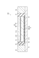
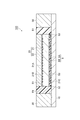
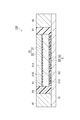
- 1 to 6 are schematic cross-sectional views showing an embodiment of an imaging module to be manufactured, respectively.
- the image pickup module 101 shown in FIG. 1 is arranged between the wiring board 10, the semiconductor component 20, the resin frame portion 30 provided on the wiring board 10 and surrounding the semiconductor component 20, and the semiconductor component 20 and the wiring board 10.
- the wiring board 10, the semiconductor component 20, and the resin frame portion 30 are integrated via the sealing portion 51 and the underfill 52.
- the connecting portion 8 is formed of the conductive adhesive composition.
- the semiconductor component 20 has a solid-state image sensor 21 having an image receiving surface S1 and a surface opposite to the image receiving surface S1 (back surface S2).
- the solid-state image sensor 21 is a wafer-level chip size package, and includes a sensor element 21A arranged in the image receiving surface S1, a color filter 21B covering the sensor element 21A, and a plurality of connection terminals 21C provided on the back surface S2. ..
- the connection terminal 21C contains metal and may be a bump.
- Specific examples of the solid-state image sensor 21 are a CCD image sensor and a CMOS image sensor.
- the sensor element 21A is, for example, a photodiode.
- the sensor element 21A is provided by the technology of wafer level chip size packaging (WLCSP).
- a plurality of color filters may be provided.
- a via electrode may be provided that penetrates between the image receiving surface S1 and the back surface S2 of the solid-state image sensor 21.
- the semiconductor component 20 further includes a plate-shaped translucent member 22 provided on the image receiving surface S1.
- the plate-shaped translucent member 22 may be an inorganic glass plate.
- the plate-shaped translucent member 22 is fixed to the semiconductor component 20 via a resin adhesive or the like.
- the thickness of the plate-shaped translucent member 22 may be, for example, 10 to 200 ⁇ m.
- the plate-shaped translucent member 22, the resin frame portion 30, and the sealing portion 51 may be flush with each other to form a flat main surface of the image pickup module 101.
- the thickness of the solid-state image sensor 21 may be, for example, 50 to 500 ⁇ m.
- the maximum width of the solid-state image sensor 21 may be, for example, 5 to 30 mm.
- the maximum width of the connection terminal 21C of the solid-state image sensor 21 may be, for example, 100 to 300 ⁇ m.
- the wiring board 10 has a plurality of connection terminals arranged on the main surface.
- the wiring board 10 may be an organic wiring board, a coreless board, or a flexible board.
- the thickness of the wiring board 10 may be, for example, 50 to 450 ⁇ m.
- the semiconductor component 20 is mounted on the wiring board 10 so that the connection terminal of the wiring board 10 and the connection terminal 21C of the solid-state image sensor 21 face each other.
- the connection portion 8 formed between the connection terminal 21C and the wiring board 10 is around the conductive portion 8A and the conductive portion 8A that electrically connect the connection terminal of the wiring board 10 and the connection terminal 21C of the solid-state image sensor 21. It is composed of the cured resin portion 8B formed in the above.
- the conductive portion 8A mainly contains the metal of the conductive particles contained in the conductive adhesive composition.
- the cured resin portion 8B mainly contains a cured product of an adhesive component containing a thermosetting resin, which was contained in the conductive adhesive composition.
- the cured resin portion 8B may contain a small amount of conductive particles as long as appropriate insulating properties are maintained.
- the wiring board 10 and the solid-state image sensor 21 are joined to each other by the connecting portion 8 and electrically connected to each other.
- the gap between the adjacent connecting portions 8 is filled with the underfill 52.
- the ratio of the cured resin portion 8B to the amount of the conductive portion 8A and the filling rate of the underfill 52 can be appropriately changed without departing from the spirit of the present invention.
- the area ratio of the conductive portion and the cured resin portion is 5:95 to 80:20. There may be.
- the ratio of the cured resin portion 8B to the amount of the conductive portion 8A is larger than the ratio in the imaging module 101, and a part of the voids between the adjacent connecting portions 8 is underfilled. Not filled by 52.
- the cured resin portion 8B is integrated with the cured resin portion 8B of the adjacent connecting portion 8 to form a semiconductor component.
- the space between 20 and the wiring board 10 is filled with the cured resin portion 8B.
- the cured resin portion 8B also functions as an underfill, the occurrence of cracks in the conductive portion 8A is suppressed.
- FIGS. 4, 5 and 6 show an example of an imaging module in which an underfill 52 formed of a sealing material different from the sealing portion 51 is not introduced.
- the sealing portion 51 fills the space between the semiconductor component 20 and the resin frame portion 30, and also fills the space between the semiconductor component 20 and the wiring board 10 between the connecting portions 8. doing.
- the image pickup module 105 shown in FIG. 5 the ratio of the cured resin portion 8B to the amount of the conductive portion 8A is relatively large.
- the integrated cured resin portion 8B fills the space between the semiconductor component 20 and the wiring board 10.
- the resin frame portion 30 may be a light-shielding member formed of a resin material. By surrounding the semiconductor component 20 with the light-shielding resin frame portion 30, it is possible to suppress the scattering of light incident on the image pickup module.
- the resin frame portion 30 can be formed by, for example, a transfer mold or the like with a thermosetting encapsulant for encapsulating a semiconductor. When light scattering is suppressed, flare and ghost can be suppressed.
- Various circuit components such as capacities and chips may be embedded inside the resin frame portion 30.
- the conductive portion 8A is reinforced by the cured resin portion 8B.
- the imaging module receives the thermal history of the temperature cycle test, the connection portion and other components are greatly distorted due to the occurrence of warpage and the like. Since the conductive portion 8A is reinforced by the cured resin portion 8B, the deformation of the wiring board 10 is stopped by the cured resin portion 8B, whereby the occurrence of cracks in the connecting portion 8 is suppressed.
- the semiconductor component 20 including the wiring board 10 and the solid-state image pickup element 21 is prepared, and a conductive adhesive is provided on the connection terminal of the wiring board 10 or on the connection terminal 21C of the solid-state image pickup element 21.
- the semiconductor component 20 is arranged on the wiring board 10 so that the connection terminal of the wiring board 10 and the connection terminal 21C of the solid-state imaging element 21 face each other through the step of arranging the composition and the conductive adhesive composition.
- a step of obtaining a temporary connector having the wiring board 10, the conductive adhesive composition, and the semiconductor component 20 and heating the temporary connector form a connecting portion 8 having a conductive portion 8A and a cured resin portion 8B.
- a step of obtaining a connection structure in which the wiring board 10 and the semiconductor component 20 are joined by the connecting portion 8 a step of providing a resin frame portion 30 surrounding the semiconductor component 20 on the wiring board 10, and a sealing portion 51. It can be produced by a method including the step of forming the underfill 52 and the underfill 52.
- the conductive adhesive composition can be applied on the connection terminal of the wiring board 10 or on the connection terminal 21C of the solid-state image sensor 21 by any method such as a dispensing method, a screen printing method, or a stamping method.
- the temporary connection can be heated by using a heating device such as an oven or a reflow oven. If necessary, the temporary connection body may be heated under pressure.
- a connecting portion 8 having a conductive portion 8A and a cured resin portion 8B is usually formed.
- the conductive portion 8A contains an agglomerate formed by fusing conductive particles melted by heating. This agglomerate joins with the wiring board and the connection terminal of the solid-state image sensor to form a metal connection path.
- the heating temperature for forming the connecting portion is a temperature equal to or higher than the melting point of the metal constituting the conductive particles, and may be, for example, 140 to 180 ° C.
- the image pickup module can be used as a member constituting various electronic devices such as a camera-equipped mobile phone and a digital camera.
- the conductive adhesive composition contains (A) conductive particles, (B) a thermosetting resin, and (C) a flux activator.
- the conductive particles contain a metal having a melting point of 220 ° C. or lower or a melting point of 200 ° C. or lower.
- the melting point of the metal contained in the conductive particles may be 180 ° C. or lower, or 150 ° C. or lower.
- the lower limit of the melting point of the metal in the conductive particles is not particularly limited, but is about 100 ° C.
- the metal contained in the conductive particles is an alloy containing two or more metal species, the melting point of the alloy may be 220 ° C. or lower.
- the metal in the conductive particles may be composed of a metal other than lead from the viewpoint of reducing the environmental load.
- the metal contained in the conductive particles includes, for example, one kind of metal selected from tin (Sn), bismuth (Bi), indium (In), and zinc (Zn), or two or more metal kinds. Examples include alloys. Since the alloy can obtain better connection reliability, platinum (Pt), gold (Au), silver (Ag), and the like can be used in the range where the melting point of the metal as a whole in the conductive particles is 200 ° C. or less. It may further contain a component having a high melting point selected from copper (Cu), nickel (Ni), palladium (Pd), aluminum (Al) and the like.
- the metal in the conductive particles is preferably composed of a metal other than lead from the viewpoint of reducing the environmental load.
- the metal contained in the conductive particles includes, for example, one kind of metal selected from tin (Sn), bismuth (Bi), indium (In), zinc (Zn) and the like, or two or more metal kinds. Examples include alloys. Since the alloy can obtain better connection reliability, platinum (Pt), gold (Au), silver (Ag), and the like can be used in the range where the melting point of the metal as a whole in the conductive particles is 200 ° C. or less. It may further contain a component having a high melting point selected from copper (Cu), nickel (Ni), palladium (Pd), aluminum (Al) and the like.
- the metals constituting the conductive particles include Sn42-Bi58 solder (melting point 138 ° C.), Sn48-In52 solder (melting point 117 ° C.), Sn42-Bi57-Ag1 solder (melting point 139 ° C.), and Sn90-Ag2-Cu0.
- Examples thereof include .5-Bi7.5 solder (melting point 189 ° C.), Sn96-Zn8-Bi3 solder (melting point 190 ° C.), and Sn91-Zn9 solder (melting point 197 ° C.). These show clear solidification behavior after melting. The solidification behavior means that the metal cools and hardens after melting.
- the conductive particles may contain Sn42-Bi58 solder. These are used alone or in combination of two or more.
- the cumulative 50% particle size D50 may be 3 to 10 ⁇ m.
- the cumulative particle size distribution here is measured by the laser diffraction / scattering method.
- D50 is 3 ⁇ m or more
- the conductive adhesive composition tends to have an appropriately low viscosity, and good workability can be ensured.
- the amount of flux activator required to obtain sufficient meltability of the conductive particles tends to be small.
- the cured resin product formed from the conductive adhesive composition tends to maintain good physical properties (adhesiveness at high temperature, etc.). Further, in the high temperature resistance test, the cured resin portion is not easily destroyed by the expansion of the conductive portion containing metal.
- the conductive adhesive composition can be easily applied to a small area connection terminal by any of a printing method, a transfer method, and a dispensing method.
- the D50 of the conductive particles may be 4 to 9 ⁇ m.
- the D50 of the conductive particles may be 5 to 8 ⁇ m.
- the cumulative 10% particle size D10 may be 2.4 ⁇ m or more.
- the amount of the required flux activator tends to be small for the same reason as described above, and therefore, for example, it is easy to maintain a high level of high temperature resistance.
- the minimum particle size Dmin in the cumulative particle size distribution may be 1.0 ⁇ m or more.
- D10 may be 2.9 ⁇ m or less, and Dmin may be 2.5 ⁇ m or less.
- the cumulative 90% particle size D90 may be 12 ⁇ m or less or 10.5 ⁇ m or less.
- the maximum particle size Dmax may be 20 ⁇ m or less.
- D90 may be 10 ⁇ m or more, and Dmax may be 13 ⁇ m or more.
- the specific surface area of the conductive particles may be 1.45 ⁇ 10 -4 to 8.45 ⁇ 10 -4 cm 2 / g.
- the conductive particles may be metal particles composed only of metal, or may be coated with nuclear particles made of a solid material other than metal such as ceramics, silica and resin material, and the surface of the nuclear particles, and has a melting point of 220 ° C. It may be a composite particle having a metal film made of the following metals, or a combination thereof.
- the content of the conductive particles may be 5 to 95% by mass with respect to the total mass of the conductive adhesive composition.
- the content of the conductive particles may be 5 to 95% by mass with respect to the total mass of the conductive adhesive composition.
- the content of the conductive particles is less than 5% by mass, the conductivity of the cured product of the conductive adhesive composition tends to decrease.
- the content of the conductive particles exceeds 95% by mass, the viscosity of the conductive adhesive composition increases, so that the workability tends to decrease.
- the proportion of the thermosetting adhesive component in the conductive adhesive composition is relatively small, the mounting reliability tends to decrease.
- the content of the conductive particles may be 30 to 90% by mass from the viewpoint of improving workability or conductivity, and 40 to 85% by mass from the viewpoint of improving the mounting reliability of the conductive adhesive composition. It may be.
- the conductive adhesive composition may contain conductive particles having a high melting point containing a metal having a melting point of 220 ° C. or lower or 200 ° C. or lower and a metal having a melting point of 220 ° C. or higher than 200 ° C.
- the metal having a melting point higher than 200 ° C. include one metal simple substance selected from Pt, Au, Ag, Cu, Ni, Pd, Al and Sn, or an alloy composed of two or more metal types.
- Specific examples of the conductive particles having a high melting point include Au powder, Ag powder, Cu powder, Ag-plated Cu powder, Sn powder, and SnAgCu powder.
- "MA05K" manufactured by Hitachi Kasei Co., Ltd., trade name
- (A) conductive particles containing a metal having a melting point of 220 ° C. or lower or 200 ° C. or lower and (a1) conductive particles containing a metal having a melting point of 200 ° C. or higher than 220 ° C. are combined, (A) a melting point of 220 ° C.
- the mass ratio ((A) :( a1)) of the conductive particles containing a metal of 200 ° C. or lower or (a1) a metal having a melting point of more than 200 ° C. is 99: 1 to 50:50. , Or may be in the range of 99: 1 to 60:40.
- thermosetting resin has an action of adhering an adherend and also acts as a binder component that binds conductive particles in a conductive adhesive composition and a filler added as needed to each other.
- thermosetting resins include thermosetting organic polymer compounds such as epoxy resins, (meth) acrylic resins, maleimide resins and cyanate resins, and precursors thereof.
- the (meth) acrylic resin indicates a methacrylic resin and an acrylic resin.
- the thermosetting resin may be a compound having a polymerizable carbon-carbon double bond represented by a (meth) acrylic resin and a maleimide resin, or an epoxy resin.
- thermosetting resins are excellent in heat resistance and adhesiveness, and can be handled in a liquid state if they are dissolved or dispersed in an organic solvent as needed, so that they are also excellent in workability.
- the thermosetting resin may be an epoxy resin.
- thermosetting resins may be used alone or in combination of two or more.
- the epoxy resin is a compound having two or more epoxy groups.
- examples of the epoxy resin include bisphenol A type epoxy resin, bisphenol F type epoxy resin, bisphenol AD type epoxy resin, and amine type epoxy resin.
- epoxy resins examples include AER-X8501 (manufactured by Asahi Kasei Kogyo Co., Ltd., trade name), R-301 (manufactured by Mitsubishi Chemical Co., Ltd., trade name), and YL-980 (trade name), which are bisphenol A type epoxy resins.
- ELM-100 (manufactured by Sumitomo Chemical Industries, Ltd., trade name); YH-434L (manufactured by Toto Kasei Co., Ltd., trade name), TETRAD-X, TETRAD-C (Both manufactured by Mitsubishi Gas Chemical Co., Ltd., product name), 630, 630LSD (both manufactured by Mitsubishi Chemical Co., Ltd., product name), Denacol EX-201 (manufactured by Nagase Kasei Kogyo Co., Ltd., product name), which is a resorcin type epoxy resin; Denacol EX-221 (manufactured by Nagase Kasei Kogyo Co., Ltd., trade name); Denacol EX-212 (manufactured by Nagase Kasei Kogyo Co., Ltd., trade name), which is a neopentyl glycol type epoxy resin; Denacol EX series (EX-810, 811, 850, 85
- E-XL-24 and E-XL-3L are epoxy resins represented by the following general formula (I). (Product name) manufactured by Kagaku Co., Ltd.
- k represents an integer from 1 to 5.
- the conductive adhesive composition may further contain an epoxy compound having one epoxy group as a reactive diluent.
- an epoxy compound having one epoxy group include PGE (manufactured by Nippon Kayaku Co., Ltd., trade name), PP-101 (manufactured by Toto Kasei Co., Ltd., trade name), ED-502, ED.
- the content thereof may be a range that does not significantly impair the effect of the present invention, and is 0.1 to 30% by mass with respect to the total amount of the epoxy resin. There may be.
- the thermosetting resin may contain a (meth) acrylic resin.
- the (meth) acrylic resin is composed of a compound having a polymerizable carbon-carbon double bond (acryloyl group or methacryloyl group). Examples of such a compound include a monoacrylate compound, a monomethacrylate compound, a diacrylate compound, and a dimethacrylate compound.
- Examples of the monoacrylate compound include methyl acrylate, ethyl acrylate, propyl acrylate, isopropyl acrylate, n-butyl acrylate, isobutyl acrylate, t-butyl acrylate, amyl acrylate, isoamyl acrylate, hexyl acrylate, heptyl acrylate, octyl acrylate, and 2-.
- Examples of the monomethacrylate compound include methyl methacrylate, ethyl methacrylate, propyl methacrylate, isopropyl methacrylate, n-butyl methacrylate, isobutyl methacrylate, t-butyl methacrylate, amyl methacrylate, isoamyl methacrylate, hexyl methacrylate, heptyl methacrylate, octyl methacrylate, 2-.
- diacrylate compound examples include ethylene glycol diacrylate, 1,4-butanediol diacrylate, 1,6-hexanediol diacrylate, 1,9-nonanediol diacrylate, 1,3-butanediol diacrylate, and neo.
- dimethacrylate compound examples include ethylene glycol dimethacrylate, 1,4-butanediol dimethacrylate, 1,6-hexanediol dimethacrylate, 1,9-nonanediol dimethacrylate, 1,3-butanediol dimethacrylate, and neo.
- thermosetting resin contains a (meth) acrylic resin
- these compounds may be polymerized in advance before use, and these compounds are mixed with conductive particles, a flux activator, etc., and polymerized at the same time as the mixing. You may. Compounds having a polymerizable carbon-carbon double bond in these molecules are used alone or in combination of two or more.
- the conductive adhesive composition may further contain a radical polymerization initiator.
- a radical polymerization initiator an organic peroxide is preferable from the viewpoint of effectively suppressing voids.
- the decomposition temperature of the organic peroxide may be 130 ° C. to 200 ° C.
- radical polymerization initiator commonly used ones can be used, and examples thereof include peroxides such as benzoyl peroxide and t-butylperoxy-2-ethylhexanoate, and azobisisobutyronitrile. And azo compounds such as azobisdimethylvaleronitrile.
- the content of the radical polymerization initiator may be 0.01 to 20% by mass, 0.1 to 10% by mass, or 0.5 to 5% by mass with respect to the total amount of the conductive adhesive composition.
- acrylic resin Commercially available (meth) acrylic resin can be used. Specific examples thereof include FINEDIC A-261 (manufactured by Dainippon Ink and Chemicals Co., Ltd., trade name) and FINEDIC A-229-30 (manufactured by Dainippon Ink and Chemicals Co., Ltd., trade name).
- the content of the thermosetting resin in the conductive adhesive composition is 1 to 60% by mass, 5 to 40% by mass, or 10 to 30% by mass with respect to the total mass of the conductive adhesive composition. May be good.
- the flux activator is a component exhibiting a function of removing an oxide film formed on the surface of conductive particles. By using such a flux activator, an oxide film that hinders melt aggregation of conductive particles is removed.
- the flux activator according to one embodiment contains a compound containing a hydroxyl group and a carboxyl group. This compound exhibits good flux activity and can exhibit reactivity with an epoxy resin that can be used as a thermosetting resin.
- the compound having a hydroxyl group and a carboxyl group may be an aliphatic dihydroxycarboxylic acid because the particle size of the conductive particles is small and the oxide film removing ability is good even when the amount of the oxide film is large.
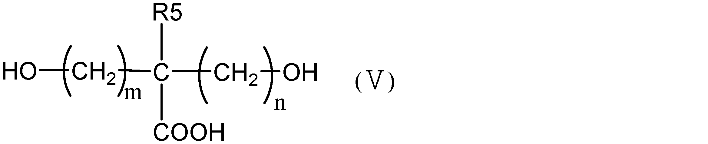
- the flux activator may contain a compound represented by the following general formula (V), tartaric acid, or a combination thereof.
- R5 represents an alkyl group having 1 to 5 carbon atoms. From the viewpoint of more effectively exerting the above-mentioned effects according to the present invention, R5 may be a methyl group, an ethyl group or a propyl group. n and m each independently represent an integer of 0 to 5. From the viewpoint of more effectively exerting the above-mentioned effects according to the present invention, n may be 0 and m may be 1, and both n and m may be 1.
- Examples of the compound represented by the above general formula (V) are 2,2-bis (hydroxymethyl) propionic acid, 2,2-bis (hydroxymethyl) butanoic acid, and 2,2-bis (hydroxymethyl). Pentanoic acid can be mentioned.
- the flux activator may contain at least one compound selected from these.
- the content of the flux activator is 1.0 to 3.9% by mass, 1.8 to 3.9% by mass, or 1.8 to 3.9% by mass with respect to the amount of the conductive particles from the viewpoint of high temperature resistance and temperature cycle test resistance. It may be 1.5 to 3.5% by mass. From the viewpoint of curability of the conductive adhesive composition and suppression of voids, the content of the flux activator may be 2.5 to 3.5% by mass with respect to the amount of the conductive particles.
- the conductive adhesive composition may further contain (D) a curing catalyst.
- the curing catalyst is a component that promotes curing of the epoxy resin.
- the curing catalyst may contain a compound having an imidazole group from the viewpoints of curability, length of pot life, heat resistance of the cured product, and the like. Examples of commercially available compounds having an imidazole group include 2P4MHZ-PW (2-phenyl-4-methyl-5-hydroxymethylimidazole), 2PHZ-PW (2-phenyl-4,5-dihydroxymethylimidazole), and C11Z.
- the content of the curing catalyst may be 0.01 to 90 parts by mass or 0.1 to 50 parts by mass with respect to 100 parts by mass of the epoxy resin.
- the content of the curing catalyst is less than 0.01 parts by mass, the curability tends to decrease, and when the content of the curing catalyst exceeds 90 parts by mass, the viscosity increases, and when handling the conductive adhesive composition. Workability tends to decrease.
- the conductive adhesive composition may further contain a curing agent in order to adjust the curing rate of the epoxy resin.
- the curing agent is not particularly limited as long as it is conventionally used, and commercially available ones are available.
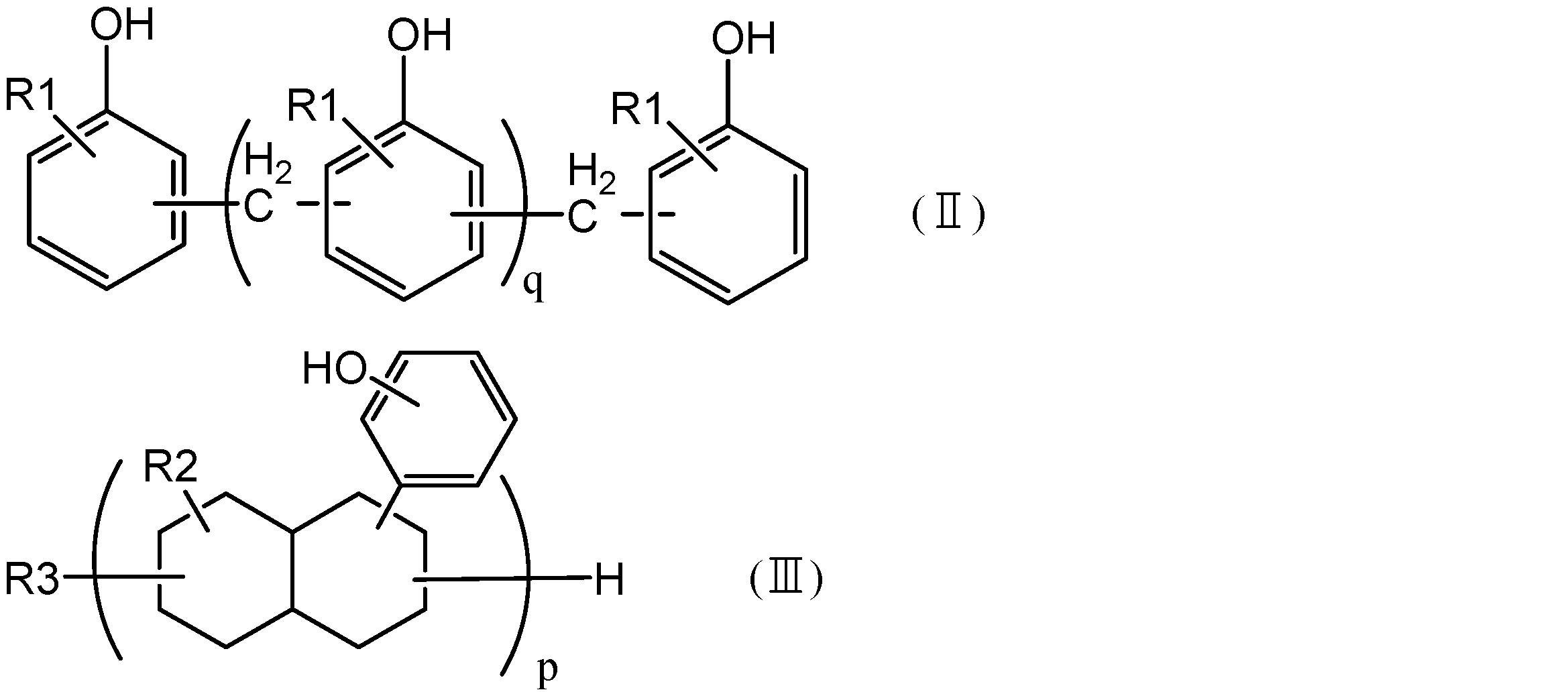
- Examples of commercially available curing agents include H-1 (manufactured by Meiwa Kasei Co., Ltd., trade name) and VR-9300 (manufactured by Mitsui Toatsu Chemical Co., Ltd., trade name), which are phenol novolac resins, and XL, which is a phenol aralkyl resin.
- each of the plurality of R1s independently represents a monovalent hydrocarbon group, and may be a methyl group or an allyl group. q indicates an integer from 1 to 5.
- R2 represents an alkyl group and may be a methyl group or an ethyl group.
- R3 represents a hydrogen atom or a monovalent hydrocarbon group, and p represents an integer of 2 to 4.
- dicyandiamide or the like which has been conventionally used as a curing agent, can also be used, and a commercially available product is available.
- commercially available products include ADH, PDH and SDH (all manufactured by Nippon Hydrazine Industry Co., Ltd., trade names), which are dibasic acid dihydrazides represented by the following general formula (IV), and reactions between epoxy resins and amine compounds.
- examples thereof include Novacure (manufactured by Asahi Kasei Kogyo Co., Ltd., trade name), which is a microcapsule type curing agent composed of a substance.
- These curing agents may be used alone or in combination of two or more.
- R4 represents a divalent aromatic group or a linear or branched alkylene group having 1 to 12 carbon atoms, and may be an m-phenylene group or a p-phenylene group.
- the conductive adhesive composition does not have to contain a curing agent substantially.
- substantially free means that the content is 0.05% by mass or less with respect to the total mass of the conductive adhesive composition.
- the conductive adhesive composition may contain a filler.
- the filler include polymer particles such as acrylic rubber and polystyrene; and inorganic particles such as diamond, boron nitride, aluminum nitride, alumina and silica. These fillers may be used alone or in admixture of two or more.
- the conductive adhesive composition contains a flexible agent for stress relaxation, a diluent for improving workability, an adhesive strength improver, a wettability improver, and a defoamer, if necessary. It may contain one or more additives selected from the group consisting of agents.
- Examples of flexible agents include liquid polybutadiene (manufactured by Ube Industries, Ltd., trade names “CTBN-1300 x 31" and “CTBN-1300 x 9", manufactured by Nippon Soda Co., Ltd., trade name "NISSO-PB-C-”. 2000 ").
- the content of the flexible agent may be 0.1 to 500 parts by mass with respect to 100 parts by mass of the thermosetting resin.
- diluents have relatively high boiling points such as butyl carbitol, butyl carbitol acetate, butyl cellosolve, carbitol, butyl celloacetate acetate, carbitol acetate, dipropylene glycol monomethyl ether, ethylene glycol diethyl ether, and ⁇ -terpineol.
- examples include organic solvents.
- the content of the diluent may be 0.1 to 30% by mass with respect to the total mass of the conductive adhesive composition.
- the adhesive strength improving agent may be a coupling agent such as a silane coupling agent or a titanium coupling agent.
- silane coupling agent examples include "KBM-573" manufactured by Shin-Etsu Chemical Co., Ltd.
- the wettability improver may be, for example, an anionic surfactant or a fluorine-based surfactant.
- the defoaming agent may be, for example, silicone oil.
- the adhesive strength improver, the wettability improver, and the antifoaming agent are used individually by 1 type or in combination of 2 or more types. These contents may be 0.1 to 10% by mass with respect to the total mass of the conductive adhesive composition.
- the conductive adhesive composition can be obtained by heating each of the above-mentioned components at once or in a plurality of times as necessary, and mixing, dissolving, pulverizing and kneading or dispersing.
- the conductive adhesive composition may be in the form of a paste in which each component is uniformly dispersed.
- Examples of the dispersion / dissolution device used in this case include a known stirrer, a raker, a three-roll device, a planetary mixer, and the like.
- the conductive adhesive composition may be in the form of a paste at 25 ° C. and have a viscosity of 5 to 400 Pa ⁇ s.
- the conductive adhesive composition of the present embodiment described above causes a short circuit between electrodes with respect to a wiring board having connection terminals such as electrode pads having a small area or electrodes arranged at a pinching pitch. It is possible to connect semiconductor parts with good conductivity.
- the connecting portion formed by the conductive adhesive composition of the present embodiment can have a conductive portion containing conductive particles and a cured resin portion formed of an insulating adhesive component. Reinforcement by the cured resin portion can contribute to the improvement of the high temperature resistance of the imaging module and the improvement of the temperature cycle test resistance.
- the present invention is not limited to the above embodiment.
- the present invention can be modified in various ways without departing from the gist thereof.
- STC-7 Sn42-Bi58 particles (D50: 8.0 ⁇ m, D10: 5.3 ⁇ m, D90: 10.3 ⁇ m, manufactured by Mitsui Mining & Smelting Co., Ltd., melting point 138 ° C.)
- STC-5 Sn42-Bi58 particles (D50: 6.4 ⁇ m, D10: 4.6 ⁇ m, D90: 8.7 ⁇ m, manufactured by Mitsui Mining & Smelting Co., Ltd., melting point 138 ° C.)
- STC-3 Sn42-Bi58 particles (D50: 4.1 ⁇ m, D10: 2.7 ⁇ m, D90: 6.0 ⁇ m, manufactured by Mitsui Mining & Smelting Co., Ltd., melting point 138 ° C.)
- ST-7 Sn42-Bi58 particles (D50: 7.1 ⁇ m, D10: 3.6 ⁇ m, D90: 10.6 ⁇ m, manufactured by Mitsui
- Conductive Adhesive Composition Example 1 15.2 parts by mass of YL980, 0.8 parts by mass of 2P4MHZ-PW and 3.0 parts by mass of BHPA were mixed and the mixture was passed through 3 rolls 3 times. Subsequently, 81 parts by mass of STC-7, which is Sn42-Bi58 particles, was added to 19 parts by mass of the mixture. The mixture was stirred using a planetary mixer and defoamed at 500 Pa or less for 10 minutes to obtain a conductive adhesive composition.
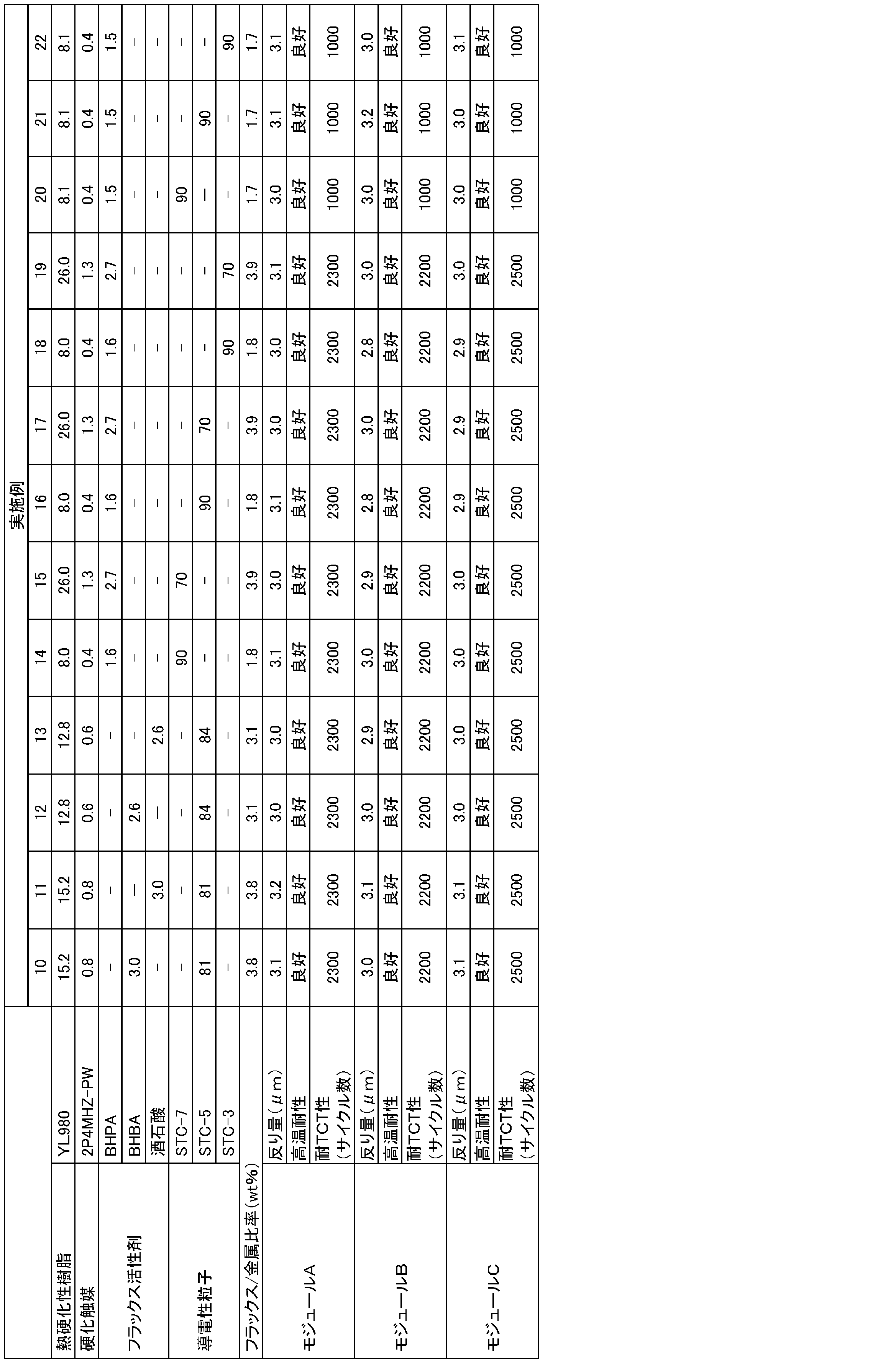
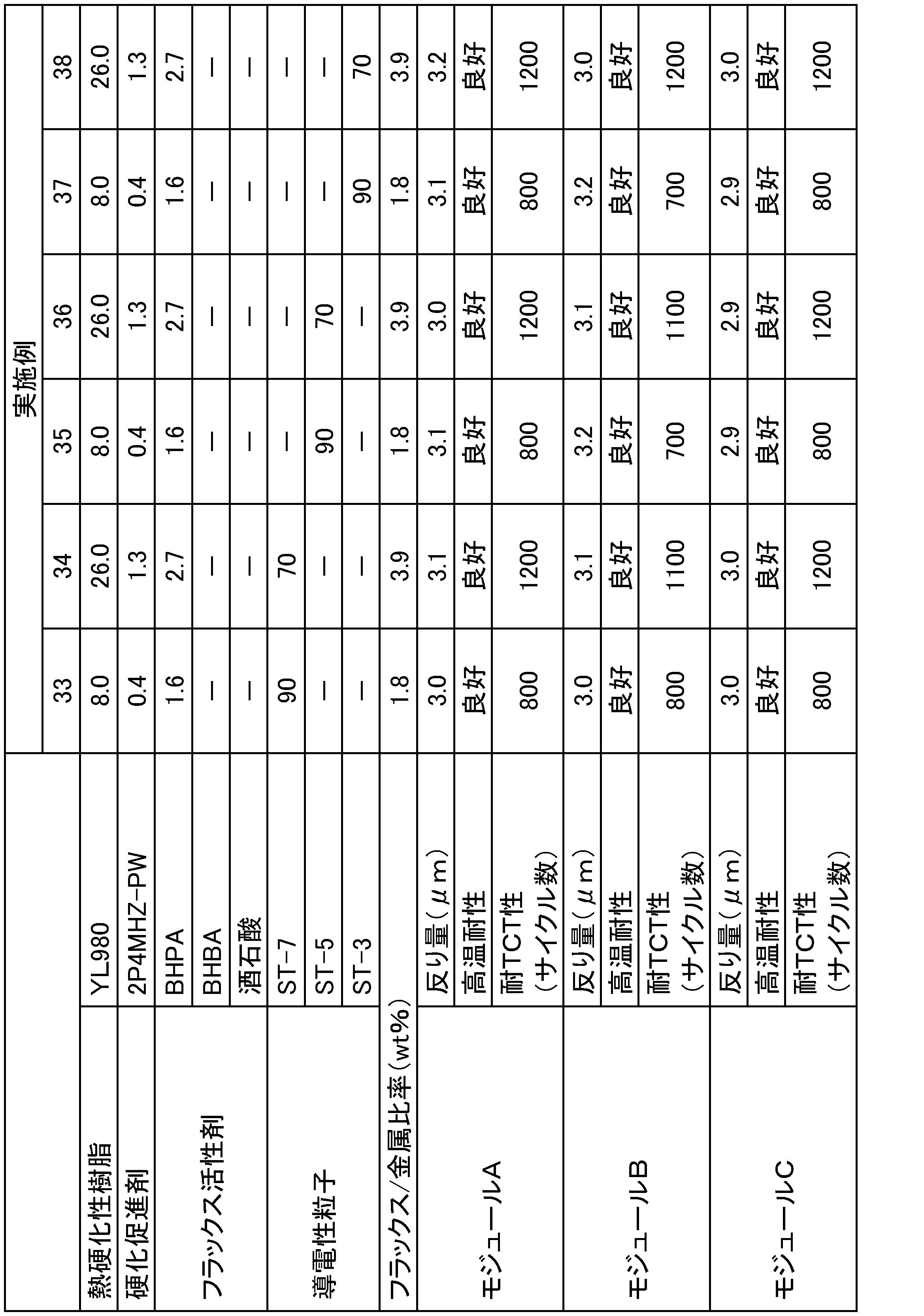
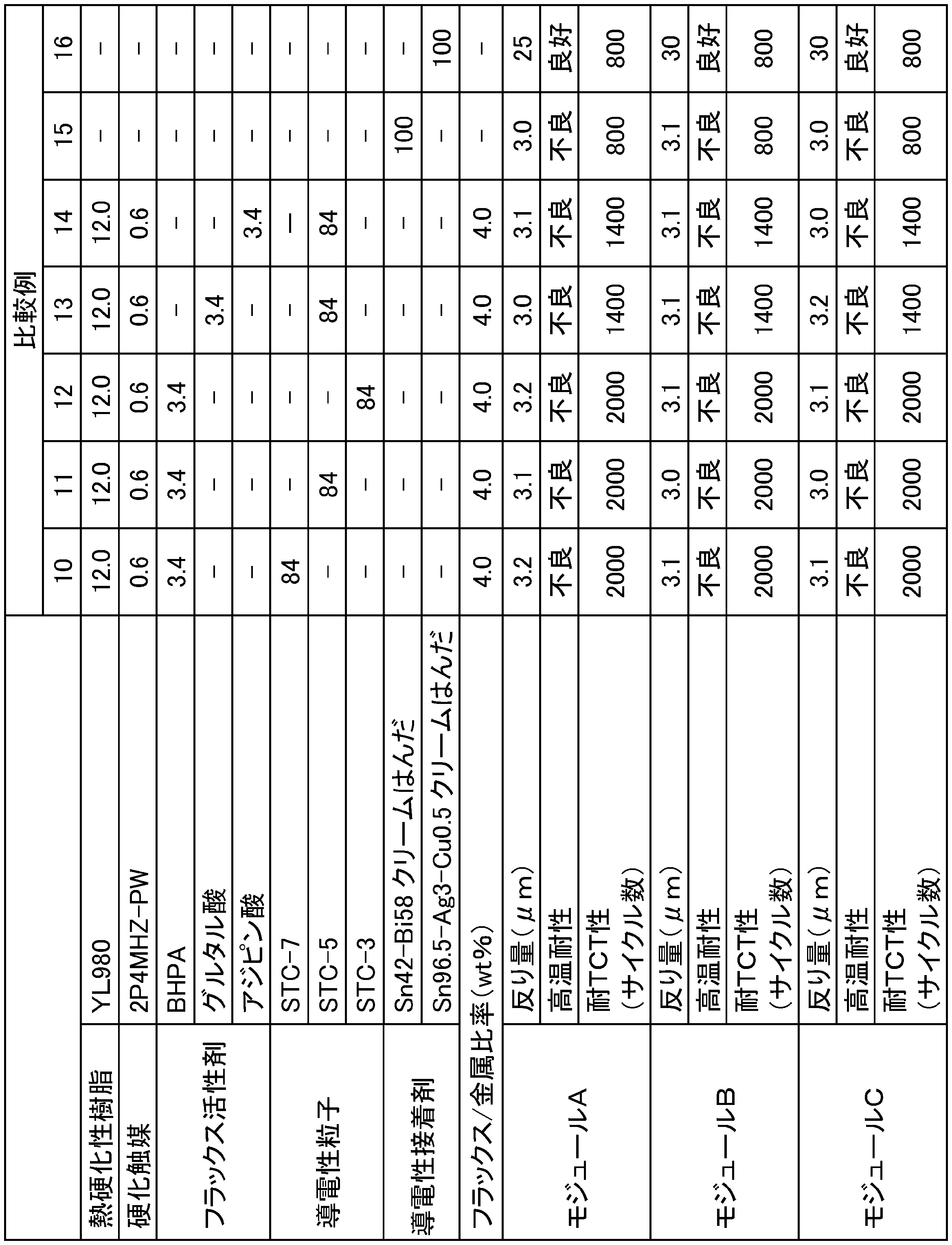
- Examples 2-39, Comparative Examples 1-14 Conductive adhesive compositions of Examples 2 to 39 and Comparative Examples 1 to 14 were obtained in the same manner as in Example 1 except that the compounding ratio (parts by mass) was changed as shown in Tables 1 to 6. ..
- Comparative Examples 15 and 16 The following commercially available conductive adhesives were prepared. Comparative Example 15: Sn42-Bi58 Cream Solder (manufactured by Senju Metal Industry Co., Ltd., Eco Solder (trade name)) Comparative Example 16: Sn96.5-Ag3-Cu0.5 cream solder (manufactured by Senju Metal Industry Co., Ltd., Eco Solder (trade name))
- evaluation module evaluation modules A to C A semiconductor component composed of a solid-state image sensor having a 5.4 mm ⁇ 7.3 mm flaky semiconductor chip and a glass plate provided on the image receiving surface of the solid-state image sensor was prepared. A plurality of bumps as connection terminals were provided on the surface (back surface) opposite to the image receiving surface of the solid-state image sensor. An organic wiring board (PI board) having a land pad provided at a position corresponding to a bump of the solid-state image sensor as a connection terminal was prepared. A resin frame portion was provided on the organic wiring board.
- PI board organic wiring board
- the conductive adhesive composition was applied to the land pad of the organic wiring board by printing using a metal mask.
- the semiconductor component was placed on the organic wiring board inside the resin frame portion so that the bumps faced the land pad via the applied conductive adhesive composition.
- a connection for connecting a semiconductor component and an organic wiring board to a conductive adhesive composition by heating the obtained temporary connection body in a nitrogen atmosphere under a condition of a maximum temperature of 150 ° C. for 10 minutes using a reflow device. The part was formed.
- a liquid encapsulant (Cell-C-3730 manufactured by Hitachi Kasei Co., Ltd.) is poured between the semiconductor component and the resin frame using a dispenser, and the liquid encapsulant is heated in a constant temperature bath at 130 ° C. for 4 hours. By curing the material, a sealing portion was formed to fill the space between the semiconductor component and the resin frame portion.
- An evaluation module was obtained by the above procedure.
- the conductive adhesive composition and the evaluation module A having different thicknesses of the connecting portion formed from the conductive adhesive composition, B and C were prepared.
- -Evaluation module A 80 ⁇ m -Evaluation module B: 120 ⁇ m -Evaluation module C: 200 ⁇ m
- the evaluation module A has the same configuration as the imaging module 104 of FIG.
- the evaluation module B has the same configuration as the imaging module 105 of FIG.
- the evaluation module C has the same configuration as the imaging module 106 of FIG.
- the shape of the surface opposite to the connection terminal of the semiconductor component used for manufacturing the warp amount evaluation module is measured using a warp measuring device (manufactured by AKROMETRIX, trade name: THERMORE PS200), and the displacement is measured. The maximum value and the minimum value were obtained, and the value of the difference was used as the initial shape value.
- the shape of the surface opposite to the connection terminal of the semiconductor component constituting the evaluation module was measured in the same manner, the maximum value and the minimum value of the displacement were obtained, and the difference value was used as the shape value after mounting. The value obtained by subtracting the initial shape value from the shape value after mounting was recorded as the amount of warpage.
- connection resistance value of the high temperature resistance evaluation module was confirmed using a simple tester and used as the initial resistance value. Then, the evaluation module was held at 150 ° C. for 96 hours using a high temperature tester. After that, the connection resistance value of the evaluation module was measured, and the rate of change of that value with respect to the initial resistance value was determined. When the rate of change was within ⁇ 5%, it was judged as “good”, and when the rate of change was greater than ⁇ 5%, it was judged as “poor”.
- connection resistance value of the TCT resistance evaluation module was measured using a simple tester and used as the initial resistance value. Then, the evaluation module is held at -55 ° C. for 30 minutes, heated to 125 ° C. for 5 minutes, held at 125 ° C. for 30 minutes, and lowered to -55 ° C. for 5 minutes using a thermal shock tester. It was subjected to a thermal shock test in which the temperature change of was one cycle. The connection resistance value of the evaluation module after the thermal shock test was measured. The connection resistance value of the evaluation module was measured while increasing the number of cycles, and the maximum number of cycles in which the rate of change with respect to the initial resistance value remained within ⁇ 10% was used as an index of TCT resistance.
- Comparative Example 17 A liquid flux material was applied to the land pad of the organic wiring board. Subsequently, without using the conductive adhesive composition, the semiconductor component was placed on the organic wiring board inside the resin frame portion so that the bumps faced the land pad. The land pad and the bump were connected by heating the obtained structure in a nitrogen atmosphere under the condition of a maximum temperature of 260 ° C. for 10 minutes using a reflow device. Next, a liquid encapsulant (Cell-C-3730 manufactured by Hitachi Kasei Co., Ltd.) is poured between the semiconductor component and the resin frame using a dispenser, and the liquid encapsulant is heated in a constant temperature bath at 130 ° C. for 4 hours.
- a liquid encapsulant Cell-C-3730 manufactured by Hitachi Kasei Co., Ltd.
- An evaluation module D was obtained by the above procedure.
- the amount of warpage, TCT resistance and high temperature resistance of the evaluation module D were evaluated by the same method as described above.
- the amount of warpage was 32 ⁇ m
- the high temperature resistance was good
- the TCT resistance was 800 cycles.
- Examples 1 to 39 showed good characteristics in terms of the amount of warpage and high temperature resistance at 150 ° C.
- Examples 1 to 23 were also excellent in terms of TCT resistance.
- the high temperature resistance at 150 ° C. was not sufficient.
- Comparative Examples 16 and 17 the amount of warpage was large.
Landscapes
- Chemical & Material Sciences (AREA)
- Organic Chemistry (AREA)
- Physics & Mathematics (AREA)
- Dispersion Chemistry (AREA)
- Spectroscopy & Molecular Physics (AREA)
- Inorganic Chemistry (AREA)
- Adhesives Or Adhesive Processes (AREA)
Abstract
Description


(A)導電性粒子
・STC-7:Sn42-Bi58粒子(D50:8.0μm、D10:5.3μm、D90:10.3μm、三井金属株式会社製、融点138℃)
・STC-5:Sn42-Bi58粒子(D50:6.4μm、D10:4.6μm、D90:8.7μm、三井金属株式会社製、融点138℃)
・STC-3:Sn42-Bi58粒子(D50:4.1μm、D10:2.7μm、D90:6.0μm、三井金属株式会社製、融点138℃)
・ST-7:Sn42-Bi58粒子(D50:7.1μm、D10:3.6μm、D90:10.6μm、三井金属株式会社製、融点138℃)
・ST-5:Sn42-Bi58粒子(D50:5.3μm、D10:2.3μm、D90:8.5μm、三井金属株式会社製、融点138℃)
・ST-3:Sn42-Bi58粒子(D50:3.1μm、D10:1.7μm、D90:5.0μm、三井金属株式会社製、融点138℃)
・Type6:Sn42-Bi58粒子(平均粒径10μm、最大粒径:18.0μm、三井金属株式会社製、融点138℃)
・Sn42-Bi57-Ag1粒子(平均粒径5μm、D10:2.2μm、D90:8.6μm)
(B)熱硬化性樹脂
・YL980(三菱化学株式会社製、ビスフェノールA型エポキシ樹脂の商品名)
(C)フラックス活性剤
・BHPA:2,2-ビス(ヒドロキシメチル)プロピオン酸
・BHBA:2,2-ビスヒドロキシメチルブタン酸
・酒石酸
・グルタル酸
・アジピン酸
(D)硬化触媒
・2P4MHZ-PW(四国化成株式会社製、イミダゾール化合物の商品名)
実施例1
15.2質量部のYL980と、0.8質量部の2P4MHZ-PWと、3.0質量部のBHPAとを混合し、混合物を3本ロールに3回通した。続いて混合物19質量部に対して、Sn42-Bi58粒子であるSTC-7を81質量部加えた。混合物をプラネタリーミキサーを用いて撹拌し、500Pa以下で10分間、脱泡処理して、導電性接着剤組成物を得た。
配合比(質量部)を表1~表6に示すように変更したこと以外は実施例1と同様にして、実施例2~39及び比較例1~14の導電性接着剤組成物を得た。
下記の市販の導電性接着剤を準備した。
比較例15:Sn42-Bi58クリームはんだ(千住金属工業株式会社製、エコソルダー(商品名))
比較例16:Sn96.5-Ag3-Cu0.5クリームはんだ(千住金属工業株式会社製、エコソルダー(商品名))
評価用モジュールA~C
5.4mm×7.3mmの薄片状の半導体チップを有する固体撮像素子と、固体撮像素子の受像面上に設けられたガラス板とから構成される半導体部品を準備した。固体撮像素子の受像面とは反対側の面(裏面)上には接続端子としての複数のバンプが設けられていた。固体撮像素子のバンプに対応する位置に設けられたランドパッドを接続端子として有する有機配線基板(PI基板)を準備した。有機配線基板上には樹脂枠部が設けられていた。
・評価用モジュールA:80μm
・評価用モジュールB:120μm
・評価用モジュールC:200μm
評価用モジュールAは図4の撮像モジュール104と同様の構成を有する。評価用モジュールBは図5の撮像モジュール105と同様の構成を有する。評価用モジュールCは図6の撮像モジュール106と同様の構成を有する。
評価用モジュールの反り量、150℃での高温耐性、及び、耐TCT性(温度サイクル試験耐性)を以下の方法で評価した。評価結果が表1~表6にまとめて示される。表中、「フラックス/金属比率(%)」は、導電性粒子の量に対するフラックス活性剤の比率(質量%)を意味する。
評価用モジュールの作製に用いた半導体部品の接続端子とは反対側の面の形状を、反り測定装置(AKROMETRIX社製、商品名:THERMOIRE PS200)を用いて測定し、変位の最大値と最小値を求め、その差の値を初期形状値とした。評価用モジュールを構成する半導体部品の接続端子とは反対側の面の形状を同様に測定し、変位の最大値と最小値を求め、その差の値を実装後形状値とした。実装後形状値から初期形状値を引いた値を反り量として記録した。
評価用モジュールの接続抵抗値を、簡易テスターを用いて確認し、初期抵抗値とした。その後、評価用モジュールを、高温試験機を用いて、150℃で96時間保持した。その後、評価用モジュールの接続抵抗値を測定し、その値の初期抵抗値に対する変化率を求めた。変化率が±5%以内であったときに「良好」と判定し、変化率が±5%よりも大きい値をであったときに「不良」と判定した。
評価用モジュールの接続抵抗値を、簡易テスターを用いて測定し、初期抵抗値とした。その後、評価用モジュールを、熱衝撃試験機を用いて、-55℃で30分間保持、125℃まで5分間で昇温、125℃で30分間保持、及び-55℃まで5分間で降温の順の温度変化を1サイクルとする熱衝撃試験に供した。熱衝撃試験後の評価用モジュールの接続抵抗値を測定した。サイクル数を増やしながら評価用モジュールの接続抵抗値を測定し、初期抵抗値に対する変化率が±10%以内にとどまる最大のサイクル数を、耐TCT性の指標とした。



有機配線基板のランドパッドに、液状フラックス材を塗布した。続いて、導電性接着剤組成物を用いることなく、バンプがランドパッドと対向するように、樹脂枠部の内側で半導体部品を有機配線基板上に載せた。得られた構造体を、リフロー装置を用いて、窒素雰囲気下、最大温度260℃の条件で10分間加熱することにより、ランドパッドとバンプとを接続した。次いで、半導体部品と樹脂枠部の間に、液状封止材(日立化成株式会社製、Cell-C-3730)をディスペンサを用いて流し込み、恒温槽130℃で4時間の加熱により液状封止材を硬化させることによって、半導体部品と樹脂枠部との間を充填する封止層を形成した。以上の手順により、評価用モジュールDを得た。
評価用モジュールDの反り量、耐TCT性及び高温耐性を上記と同様の方法で評価した。反り量は32μm、高温耐性は良好、耐TCT性は800サイクルであった。
Claims (17)
- 配線基板と該配線基板上に搭載された、受像面を有する固体撮像素子を含む半導体部品とを備える撮像モジュールを製造するために用いられる導電性接着剤組成物であって、
前記固体撮像素子がウエハレベルチップサイズパッケージであり、
前記配線基板が複数の接続端子を有し、前記固体撮像素子が、前記受像面とは反対側の面上に設けられた複数の接続端子を有し、前記半導体部品が、前記配線基板の接続端子と前記固体撮像素子の接続端子とが対向する向きで前記配線基板上に搭載され、
前記撮像モジュールが、前記配線基板の接続端子と前記固体撮像素子の接続端子とを電気的に接続する導電部と該導電部の周囲に形成された硬化樹脂部とを有する接続部を更に備え、
当該導電性接着剤組成物が、(A)金属を含む導電性粒子、(B)熱硬化性樹脂、及び(C)フラックス活性剤を含有し、
前記フラックス活性剤が、水酸基及びカルボキシル基を有する化合物を含み、
前記フラックス活性剤の含有量が、前記導電性粒子の質量に対して1.0~3.9質量%であり、
当該導電性接着剤組成物によって前記接続部が形成される、
導電性接着剤組成物。 - 前記撮像モジュールが、前記配線基板上に設けられ前記半導体部品を囲む樹脂枠部を更に備える、請求項1に記載の導電性接着剤組成物。
- 前記撮像モジュールが、前記半導体部品と前記樹脂枠部との間を充填する封止部を更に備える、請求項2に記載の導電性接着剤組成物。
- 前記撮像モジュールが、前記半導体部品と前記配線基板との間で複数の前記接続部の間を充填するアンダーフィルを更に有する、請求項1~3のいずれか一項に記載の導電性接着剤組成物。
- 前記フラックス活性剤の含有量が、前記導電性粒子の質量に対して1.8~3.9質量%である、請求項1~4のいずれか一項に記載の導電性接着剤組成物。
- 前記導電性粒子が融点220℃以下の金属を含む、請求項1~5のいずれか一項に記載の導電性接着剤組成物。
- 前記導電性粒子が融点200℃以下の金属を含む、請求項1~5のいずれか一項に記載の導電性接着剤組成物。
- 前記導電性粒子が、ビスマス、インジウム、スズ及び亜鉛から選ばれる少なくとも1種の金属を含む、請求項1~5のいずれか一項に記載の導電性接着剤組成物。
- 前記導電性粒子の体積基準の累積粒度分布において、累積50%粒径D50が3~10μmである、請求項1~8のいずれか一項に記載の導電性接着剤組成物。
- 前記導電性粒子の体積基準の累積粒度分布において、累積10%粒径D10が2.4μm以上である、請求項1~9のいずれか一項に記載の導電性接着剤組成物。
- 前記導電性粒子の体積基準の累積粒度分布において、累積90%粒径D90が10.5μm以下である、請求項1~10のいずれか一項に記載の導電性接着剤組成物。
- 前記導電性粒子の体積基準の累積粒度分布において、最小粒径Dminが1.0μm以上である、請求項1~11のいずれか一項に記載の導電性接着剤組成物。
- 前記導電性粒子の体積基準の累積粒度分布において、最大粒径Dmaxが20μm以下である、請求項1~12のいずれか一項に記載の導電性接着剤組成物。
- 前記熱硬化性樹脂がエポキシ樹脂を含む、請求項1~13のいずれか一項に記載の導電性接着剤組成物。
- (D)硬化触媒を更に含有する、請求項14に記載の導電性接着剤組成物。
- 当該導電性接着剤組成物が、25℃でペースト状である、請求項1~15のいずれか一項に記載の導電性接着剤組成物。
- 複数の接続端子を有する配線基板、及び、受像面を有する固体撮像素子を含む半導体部品であって、前記固体撮像素子が前記受像面とは反対側の面上に設けられた複数の接続端子を有する、半導体部品を準備し、前記配線基板の接続端子上又は前記固体撮像素子の接続端子上に、請求項1~16のいずれか一項に記載の導電性接着剤組成物を配置する工程と、
前記導電性接着剤組成物を介して前記配線基板の接続端子と前記固体撮像素子の接続端子とが対向するように、前記配線基板上に前記半導体部品を配置して、前記配線基板、前記導電性接着剤組成物及び前記半導体部品を有する仮接続体を得る工程と、
前記仮接続体を加熱することによって、前記導電性接着剤組成物中の導電性粒子から形成された導電部であって、前記配線基板の接続端子と前記固体撮像素子の接続端子とを電気的に接続する導電部、及び、該導電部の周囲に形成された硬化樹脂部を有する接続部を形成する工程と、
を含む、撮像モジュールを製造する方法。
Priority Applications (1)
| Application Number | Priority Date | Filing Date | Title |
|---|---|---|---|
| JP2022500404A JP7704137B2 (ja) | 2020-02-12 | 2021-02-08 | 導電性接着剤組成物、及び、撮像モジュールを製造する方法 |
Applications Claiming Priority (2)
| Application Number | Priority Date | Filing Date | Title |
|---|---|---|---|
| JP2020021336 | 2020-02-12 | ||
| JP2020-021336 | 2020-02-12 |
Publications (1)
| Publication Number | Publication Date |
|---|---|
| WO2021161964A1 true WO2021161964A1 (ja) | 2021-08-19 |
Family
ID=77292236
Family Applications (1)
| Application Number | Title | Priority Date | Filing Date |
|---|---|---|---|
| PCT/JP2021/004618 Ceased WO2021161964A1 (ja) | 2020-02-12 | 2021-02-08 | 導電性接着剤組成物、及び、撮像モジュールを製造する方法 |
Country Status (3)
| Country | Link |
|---|---|
| JP (1) | JP7704137B2 (ja) |
| TW (1) | TWI872202B (ja) |
| WO (1) | WO2021161964A1 (ja) |
Families Citing this family (1)
| Publication number | Priority date | Publication date | Assignee | Title |
|---|---|---|---|---|
| TWI909298B (zh) * | 2024-01-05 | 2025-12-21 | 財團法人工業技術研究院 | 翹曲抑制的元件內埋結構 |
Citations (4)
| Publication number | Priority date | Publication date | Assignee | Title |
|---|---|---|---|---|
| JP2005136144A (ja) * | 2003-10-30 | 2005-05-26 | Kyocera Corp | 固体撮像装置 |
| JP2015026519A (ja) * | 2013-07-26 | 2015-02-05 | 京セラケミカル株式会社 | 導電性樹脂組成物および半導体装置 |
| JP2017112312A (ja) * | 2015-12-18 | 2017-06-22 | 日立化成株式会社 | 導電性接着剤組成物、接続構造体及び半導体発光素子搭載フレキシブル配線基板 |
| JP2018168336A (ja) * | 2017-03-30 | 2018-11-01 | 太陽インキ製造株式会社 | 導電性接着剤、硬化物、電子部品および電子部品の製造方法 |
Family Cites Families (1)
| Publication number | Priority date | Publication date | Assignee | Title |
|---|---|---|---|---|
| WO2019013336A1 (ja) | 2017-07-14 | 2019-01-17 | 日立化成株式会社 | 導電性接着剤組成物及びこれを用いた接続構造体 |
-
2021
- 2021-02-08 TW TW110104786A patent/TWI872202B/zh active
- 2021-02-08 WO PCT/JP2021/004618 patent/WO2021161964A1/ja not_active Ceased
- 2021-02-08 JP JP2022500404A patent/JP7704137B2/ja active Active
Patent Citations (4)
| Publication number | Priority date | Publication date | Assignee | Title |
|---|---|---|---|---|
| JP2005136144A (ja) * | 2003-10-30 | 2005-05-26 | Kyocera Corp | 固体撮像装置 |
| JP2015026519A (ja) * | 2013-07-26 | 2015-02-05 | 京セラケミカル株式会社 | 導電性樹脂組成物および半導体装置 |
| JP2017112312A (ja) * | 2015-12-18 | 2017-06-22 | 日立化成株式会社 | 導電性接着剤組成物、接続構造体及び半導体発光素子搭載フレキシブル配線基板 |
| JP2018168336A (ja) * | 2017-03-30 | 2018-11-01 | 太陽インキ製造株式会社 | 導電性接着剤、硬化物、電子部品および電子部品の製造方法 |
Also Published As
| Publication number | Publication date |
|---|---|
| TW202220134A (zh) | 2022-05-16 |
| JP7704137B2 (ja) | 2025-07-08 |
| JPWO2021161964A1 (ja) | 2021-08-19 |
| TWI872202B (zh) | 2025-02-11 |
Similar Documents
| Publication | Publication Date | Title |
|---|---|---|
| KR101397891B1 (ko) | 접착제 조성물 및 그것을 이용한 전자부품 탑재 기판 및 반도체장치 | |
| US9862866B2 (en) | Electrically conductive adhesive composition, connection structure, solar battery module, and method for producing same | |
| JP5468199B2 (ja) | 導電性接着剤組成物、電子部品搭載基板及び半導体装置 | |
| KR20120065446A (ko) | 도전성 접착제, 태양 전지 및 그 제조 방법, 그리고 태양 전지 모듈 | |
| JP5900349B2 (ja) | 導電性接着剤組成物、接続体及び太陽電池モジュール | |
| JP5900350B2 (ja) | 導電性接着剤組成物、接続体及び太陽電池モジュール | |
| JP7331693B2 (ja) | 導電性接着剤組成物及びこれを用いた接続構造体 | |
| JP6782413B2 (ja) | 導電性接着剤組成物、接続構造体及び半導体発光素子搭載フレキシブル配線基板 | |
| JP2011023577A (ja) | 導電性接着剤組成物、これを用いた接続体、太陽電池セルの製造方法及び太陽電池モジュール | |
| KR20130120459A (ko) | 태양 전지 모듈 | |
| WO2012043491A1 (ja) | 太陽電池モジュール | |
| TWI891726B (zh) | 導電性接著劑組成物及製造連接結構體的方法 | |
| JP7704137B2 (ja) | 導電性接着剤組成物、及び、撮像モジュールを製造する方法 | |
| JP7212831B2 (ja) | 導電性接着剤組成物及びこれを用いた接続構造体 | |
| JP2018178125A (ja) | 導電性接着剤組成物、接続体、太陽電池モジュール及びその製造方法 | |
| JP7647178B2 (ja) | 導電性接着剤組成物、有機エレクトロニクスデバイス、及び有機エレクトロニクスデバイスを製造する方法 | |
| JP7405196B2 (ja) | 導電性接着剤組成物、接続構造体及び半導体発光素子搭載フレキシブル配線基板 | |
| JP2020188268A (ja) | 導電性接着剤組成物、接続構造体及び半導体発光素子搭載フレキシブル配線基板 |
Legal Events
| Date | Code | Title | Description |
|---|---|---|---|
| 121 | Ep: the epo has been informed by wipo that ep was designated in this application |
Ref document number: 21753766 Country of ref document: EP Kind code of ref document: A1 |
|
| ENP | Entry into the national phase |
Ref document number: 2022500404 Country of ref document: JP Kind code of ref document: A |
|
| NENP | Non-entry into the national phase |
Ref country code: DE |
|
| 32PN | Ep: public notification in the ep bulletin as address of the adressee cannot be established |
Free format text: NOTING OF LOSS OF RIGHTS PURSUANT TO RULE 112(1) EPC (EPO FORM 1205A DATED 02/12/2022) |
|
| 122 | Ep: pct application non-entry in european phase |
Ref document number: 21753766 Country of ref document: EP Kind code of ref document: A1 |