WO2021152879A1 - 半導体装置及びエッチング方法 - Google Patents
半導体装置及びエッチング方法 Download PDFInfo
- Publication number
- WO2021152879A1 WO2021152879A1 PCT/JP2020/023359 JP2020023359W WO2021152879A1 WO 2021152879 A1 WO2021152879 A1 WO 2021152879A1 JP 2020023359 W JP2020023359 W JP 2020023359W WO 2021152879 A1 WO2021152879 A1 WO 2021152879A1
- Authority
- WO
- WIPO (PCT)
- Prior art keywords
- insulating film
- gas
- layer
- semiconductor device
- etching method
- Prior art date
- Legal status (The legal status is an assumption and is not a legal conclusion. Google has not performed a legal analysis and makes no representation as to the accuracy of the status listed.)
- Ceased
Links
Images














Classifications
-
- H—ELECTRICITY
- H10—SEMICONDUCTOR DEVICES; ELECTRIC SOLID-STATE DEVICES NOT OTHERWISE PROVIDED FOR
- H10P—GENERIC PROCESSES OR APPARATUS FOR THE MANUFACTURE OR TREATMENT OF DEVICES COVERED BY CLASS H10
- H10P50/00—Etching of wafers, substrates or parts of devices
- H10P50/20—Dry etching; Plasma etching; Reactive-ion etching
- H10P50/28—Dry etching; Plasma etching; Reactive-ion etching of insulating materials
- H10P50/282—Dry etching; Plasma etching; Reactive-ion etching of insulating materials of inorganic materials
- H10P50/283—Dry etching; Plasma etching; Reactive-ion etching of insulating materials of inorganic materials by chemical means
-
- H—ELECTRICITY
- H10—SEMICONDUCTOR DEVICES; ELECTRIC SOLID-STATE DEVICES NOT OTHERWISE PROVIDED FOR
- H10W—GENERIC PACKAGES, INTERCONNECTIONS, CONNECTORS OR OTHER CONSTRUCTIONAL DETAILS OF DEVICES COVERED BY CLASS H10
- H10W20/00—Interconnections in chips, wafers or substrates
- H10W20/01—Manufacture or treatment
- H10W20/071—Manufacture or treatment of dielectric parts thereof
- H10W20/074—Manufacture or treatment of dielectric parts thereof of dielectric parts comprising thin functional dielectric layers, e.g. dielectric etch-stop, barrier, capping or liner layers
- H10W20/076—Manufacture or treatment of dielectric parts thereof of dielectric parts comprising thin functional dielectric layers, e.g. dielectric etch-stop, barrier, capping or liner layers in via holes or trenches
-
- H—ELECTRICITY
- H10—SEMICONDUCTOR DEVICES; ELECTRIC SOLID-STATE DEVICES NOT OTHERWISE PROVIDED FOR
- H10W—GENERIC PACKAGES, INTERCONNECTIONS, CONNECTORS OR OTHER CONSTRUCTIONAL DETAILS OF DEVICES COVERED BY CLASS H10
- H10W20/00—Interconnections in chips, wafers or substrates
- H10W20/01—Manufacture or treatment
- H10W20/071—Manufacture or treatment of dielectric parts thereof
- H10W20/081—Manufacture or treatment of dielectric parts thereof by forming openings in the dielectric parts
-
- H—ELECTRICITY
- H10—SEMICONDUCTOR DEVICES; ELECTRIC SOLID-STATE DEVICES NOT OTHERWISE PROVIDED FOR
- H10W—GENERIC PACKAGES, INTERCONNECTIONS, CONNECTORS OR OTHER CONSTRUCTIONAL DETAILS OF DEVICES COVERED BY CLASS H10
- H10W20/00—Interconnections in chips, wafers or substrates
- H10W20/40—Interconnections external to wafers or substrates, e.g. back-end-of-line [BEOL] metallisations or vias connecting to gate electrodes
-
- H—ELECTRICITY
- H10—SEMICONDUCTOR DEVICES; ELECTRIC SOLID-STATE DEVICES NOT OTHERWISE PROVIDED FOR
- H10P—GENERIC PROCESSES OR APPARATUS FOR THE MANUFACTURE OR TREATMENT OF DEVICES COVERED BY CLASS H10
- H10P14/00—Formation of materials, e.g. in the shape of layers or pillars
- H10P14/60—Formation of materials, e.g. in the shape of layers or pillars of insulating materials
- H10P14/65—Formation of materials, e.g. in the shape of layers or pillars of insulating materials characterised by treatments performed before or after the formation of the materials
- H10P14/6516—Formation of materials, e.g. in the shape of layers or pillars of insulating materials characterised by treatments performed before or after the formation of the materials of treatments performed after formation of the materials
- H10P14/6518—Formation of materials, e.g. in the shape of layers or pillars of insulating materials characterised by treatments performed before or after the formation of the materials of treatments performed after formation of the materials by introduction of substances into an already-existing insulating layer
- H10P14/6519—Formation of materials, e.g. in the shape of layers or pillars of insulating materials characterised by treatments performed before or after the formation of the materials of treatments performed after formation of the materials by introduction of substances into an already-existing insulating layer the substance being oxygen
- H10P14/6522—Formation of materials, e.g. in the shape of layers or pillars of insulating materials characterised by treatments performed before or after the formation of the materials of treatments performed after formation of the materials by introduction of substances into an already-existing insulating layer the substance being oxygen introduced into a nitride material, e.g. changing SiN to SiON
Definitions
- the technology according to the present disclosure (the present technology) relates to a semiconductor device and an etching method.
- Patent Document 1 describes an atomic layer by repeating a procedure of generating a plasma of a fluorocarbon-based gas and a procedure of generating a plasma of an argon (Ar) gas using a silicon oxide film (SiO 2 film) as a film to be etched.
- the etching method for removing each is disclosed.
- a silicon nitride film may be used as an etching stopper when processing contact holes in a semiconductor device.
- SiN film silicon nitride film
- a recess may be formed in the semiconductor layer under the SiN film, and a residual defect may be generated at the bottom of the recess to increase the dark current.
- An object of the present technology is to provide a semiconductor device and an etching method capable of improving defects caused by etching during contact hole processing of the semiconductor device.
- the semiconductor device is embedded in a semiconductor layer containing silicon, a first insulating film provided on the semiconductor layer and having an opening, and an opening of the first insulating film, and is embedded in the semiconductor layer.
- the gist is that a conductive layer in contact with the lower end and an altered layer provided between the first insulating film and the conductive layer and containing oxygen are provided.
- the first polymer film is adsorbed on the insulating film provided on the semiconductor layer containing silicon by the plasma of the first gas, and the first polymerization is carried out by the plasma of the second gas.
- the film is removed, the upper surface of the insulating film exposed after the first polymer film is removed is oxidized to form an altered layer, and the second polymer film is adsorbed on the altered layer by the plasma of the third gas, and the fourth polymer film is adsorbed on the altered layer.
- the gist includes removing the second polymer film and the altered layer by gas plasma.
- FIG. 6A of the etching method which concerns on 1st Embodiment It is a partially enlarged view of FIG. 7A. It is a process cross-sectional view following FIG. 7A of the etching method which concerns on 1st Embodiment. It is a partially enlarged view of FIG. 8A. It is a process cross-sectional view following FIG. 8A of the etching method which concerns on 1st Embodiment.
- FIG. 9A is a partially enlarged view of FIG. 9A. It is a process cross-sectional view following FIG. 9A of the etching method which concerns on 1st Embodiment. It is a graph which shows the Ar ion invasion simulation result.
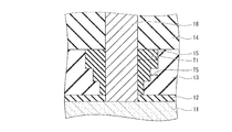
- the semiconductor device includes a semiconductor layer 11 containing silicon (Si), an insulating film (lower layer insulating film) 12 provided on the semiconductor layer 11, and a lower layer insulating film 12.
- An insulating film (intermediate insulating film) 13 provided on the intermediate insulating film 13 and an insulating film (upper layer insulating film) 14 provided on the intermediate insulating film 13 are provided.
- the semiconductor layer 11 is made of, for example, silicon (Si).
- the semiconductor layer 11 may be composed of a Si substrate, or may be composed of an epitaxial growth layer epitaxially grown on the Si substrate.
- the semiconductor layer 11 may be composed of a compound semiconductor such as silicon carbide (SiC) or silicon germanium (SiGe).
- the lower insulating film 12 is composed of, for example, a natural oxide film made of a silicon oxide film (SiO 2 film).
- the thickness of the lower insulating film 12 is, for example, about 1 nm, but the thickness is not limited to this.
- the semiconductor layer 11 and the intermediate insulating film 13 may be in direct contact with each other without the lower insulating film 12.
- the intermediate insulating film 13 is made of, for example, a silicon nitride film (Si 3 N 4 film). The thickness of the intermediate insulating film 13 is, for example, about 30 to 300 nm, but is not limited to this.
- the upper insulating film 14 is made of, for example, a silicon oxide film (SiO 2 film). The thickness of the upper insulating film 14 is, for example, about 30 to 300 nm, but is not limited to this. The upper insulating film 14 may be omitted.
- the lower insulating film 12, the intermediate insulating film 13, and the upper insulating film 14 are provided with openings (contact holes) that expose a part of the upper surface of the semiconductor layer 11.
- the diameter of the openings of the lower insulating film 12, the intermediate insulating film 13, and the upper insulating film 14 is, for example, about 30 to 100 nm, but is not limited thereto.
- a conductive layer 18 is embedded in the openings of the lower insulating film 12, the intermediate insulating film 13, and the upper insulating film 14. The lower end of the conductive layer 18 is in contact with the upper surface of the semiconductor layer 11.
- the conductive layer 18 is made of a metal material such as copper (Cu), aluminum (Al), or tungsten (W).
- wiring or the like is connected to the upper end of the conductive layer 18.
- the conductive layer 18 functions as a contact or via that electrically connects the semiconductor layer 11 to wiring or the like.
- the planar pattern of the conductive layer 18 is, for example, rectangular, but may be circular or groove-shaped.
- a alteration layer (modified layer) 15 is formed between the intermediate insulating film 13 and the conductive layer 18 so as to surround the side surface of the conductive layer 18.
- the inner side surface (inner peripheral surface) of the altered layer 15 is in contact with the side surface of the conductive layer 18.
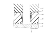
- the thickness T1 in the circumferential direction (left-right direction in FIG. 1) sandwiched between the intermediate insulating film 13 of the altered layer 15 and the conductive layer 18 becomes thinner as it is closer to the semiconductor layer 11.
- the outer side surface (outer peripheral surface) of the altered layer 15 in contact with the intermediate insulating film 13 has a stepped shape.
- FIG. 1 illustrates a case where the steps T2 in the shape of a staircase are substantially equal. Further, in FIG. 1, a case where the number of steps in the step shape of the altered layer 15 is 6 is illustrated, but the number of steps is not particularly limited, and may be 1 step, 1 to 5 steps, or 7 steps or more.
- the alteration layer 15 is composed of a region obtained by oxidizing (modifying) the intermediate insulating film 13.
- the alteration layer 15 is a layer containing oxygen, and is made of, for example, silicon oxide (SiO x ) such as silicon monoxide (SiO) and silicon dioxide (SiO 2 ) or silicon oxynitride (SiON).
- SiO x silicon oxide
- SiO 2 silicon dioxide
- SiON silicon oxynitride
- the oxygen concentration contained in the altered layer 15 is inclined from the inside to the outside so that the side surface side of the altered layer 15 in contact with the conductive layer 18 is made of SiO x and the side surface side of the altered layer 15 in contact with the intermediate insulating film 13 is made of SiON. You may be doing it.
- the passivation property of Si 3 N 4 is higher than the passivation property of SiON, and the passivation property of SiON is higher than the passivation property of SiO x . Therefore, the passivation property of the intermediate insulating film 13 made of Si 3 N 4 is higher than the passivation property of the altered layer 15 made of SiON or SiO x.
- the relative permittivity (7.0) of Si 3 N 4 is higher than the relative permittivity (4.2) of SiON or SiO x. Therefore, the relative permittivity of the intermediate insulating film 13 made of Si 3 N 4 is higher than the relative permittivity of the altered layer 15 made of SiON or SiO x.
- the pressure resistance of SION x is higher than the pressure resistance of SiON, and the pressure resistance of SION is higher than the pressure resistance of Si 3 N 4 . Therefore, the pressure resistance of the altered layer 15 made of SiON or SiO x is higher than the pressure resistance of the intermediate insulating film 13 made of Si 3 N 4.
- the alteration layer 15 containing oxygen is provided between the intermediate insulating film 13 and the conductive layer 18, it is lower than the case where the alteration layer 15 is not present.
- the dielectric constant can be increased. Therefore, the capacity can be reduced and the speed of the device can be increased.
- the withstand voltage of the altered layer 15 is higher than the withstand voltage of the intermediate insulating film 13, the withstand voltage can be improved and the leakage current can be reduced as compared with the case where the altered layer 15 is not provided.
- the thickness T1 in the circumferential direction of the altered layer 15 becomes thinner as it is closer to the semiconductor layer 11, the passivation property against moisture and gas can be improved in the vicinity of the semiconductor layer 11 and deterioration of device characteristics is prevented. be able to.
- oxidation of the semiconductor layer 11 in the portion exposed to the contact hole can be suppressed, and an increase in contact resistance can be suppressed.
- the plasma processing apparatus includes a processing container 21 for accommodating the object to be processed 100.
- a lower electrode 23 on which the object to be processed 100 is placed and an upper electrode 22 arranged to face the lower electrode 23 are arranged.
- High-frequency power supplies 27 and 28 are connected to the lower electrode 23 and the upper electrode 22, respectively.
- the high-frequency power supply 27 generates high-frequency power (high-frequency voltage) for drawing ions into the object to be processed 100.
- the high frequency power supply 28 generates high frequency power for plasma generation.
- a gas supply unit 24 and an exhaust unit 26 are connected to the processing container 21.
- the gas supply unit 24 selectively supplies various gases such as processing gas into the processing container 21 while adjusting the flow rate.
- the exhaust unit 26 is composed of a vacuum pump such as a turbo molecular pump, and decompresses the inside of the processing container 21.
- the control unit 25 is electrically connected to the gas supply unit 24, the exhaust unit 26, and the high-frequency power supplies 27 and 28.
- the control unit 25 controls the gas selection and flow rate of the gas supply unit 24, the exhaust amount of the exhaust unit 26, the power supply amount from the high frequency power supplies 27 and 28, and the like. Note that the plasma processing apparatus according to the first embodiment shown in FIG. 2 is schematic, and actually includes various parts (not shown).
- FIG. 6A and 6B show the same process
- FIG. 6B is an enlarged view of a portion A surrounded by a broken line in FIG. 6A. 7A and 7B, 8A and 8B, 9A and 9B have the same relationship as those of 6A and 6B.
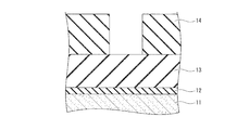
- the object to be processed (semiconductor wafer) to be processed by the etching method of the semiconductor device according to the first embodiment is prepared.
- the semiconductor wafer includes a semiconductor layer 11, a lower insulating film 12 provided on the semiconductor layer 11, and an intermediate insulating film (etched film) 13 provided on the lower insulating film 12.
- An upper insulating film 14 provided on the intermediate insulating film 13 is provided.
- the lower insulating film 12 may not be formed.
- a part of the upper insulating film 14 is selectively removed by using a photolithography technique and an etching technique to form an opening 14a that exposes a part of the upper surface of the intermediate insulating film 13.
- the semiconductor wafer shown in FIG. 4 is placed on the lower electrode 23 of the processing container 21 as the object to be processed 100.
- the upper insulating film 14 as an etching mask, a part of the upper part of the intermediate insulating film 13 is selectively removed by ordinary dry etching such as reactive ion etching (RIE).
- RIE reactive ion etching
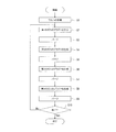
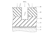
- the gas supply unit 24 shown in FIG. 2 supplies the first gas into the processing container 21 to generate plasma of the first gas.
- the first gas contains, for example, a CH x Fy- based gas containing carbon (C), fluorine (F) and hydrogen (H).
- Specific examples of the first gas include trifluoromethane (CHF 3 ) gas, difluoromethane (CH 2 F 2 ) gas, and fluoromethane (CH 3 F) gas.
- a rare gas such as argon (Ar) or an inert gas composed of nitrogen (N 2 ) may be supplied into the processing container 21 to be appropriately diluted.
- the process conditions for generating the plasma of the first gas in step S2 are, for example, the pressure in the processing container 21 is about 20 to 30 mTorr, the power of the upper electrode 22 is about 400 to 600 W, the high frequency voltage is 0 V, and the flow rate of the first gas is.
- the Ar gas flow rate is set to about 5 to 15 sccm, the Ar gas flow rate is set to about 400 to 600 sccm, and the processing time is set to about 5 to 20 seconds.
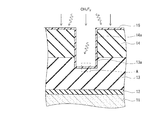
- the ions (indicated by straight arrows) and radicals (indicated by wavy arrows) contained in the plasma of the first gas are formed between the upper surface of the upper insulating film 14 and the side surface of the opening 14a.
- the first polymer film 16 is deposited on the side surface and the bottom surface of the recess 13a of the insulating film 13.
- the first polymerized film 16 is adsorbed on the surface of the intermediate insulating film 13 located in the recess 13a of the intermediate insulating film 13.
- the first polymer film 16 is made of, for example, a polymer containing carbon (C), fluorine (F) and hydrogen (H).
- the first polymerized film 16 is made of, for example, hydrofluorocarbon (HFC).
- step S3 of FIG. 3 the exhaust unit 26 shown in FIG. 2 purges the inside of the processing container 21 to exhaust the first gas supplied in step S2.
- the inside of the processing container 21 may be evacuated, or a purge gas such as Ar gas may be supplied into the processing container 21.
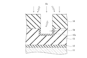
- the gas supply unit 24 shown in FIG. 2 supplies the second gas into the processing container 21 to generate plasma of the second gas.
- the second gas is a gas containing oxygen (O).
- oxygen (O 2 ) gas include oxygen (O 2 ) gas, carbon monoxide (CO) gas, carbon dioxide (CO 2 ) gas, nitric oxide (NO) gas, and nitrogen dioxide (NO 2 ) gas.
- a rare gas such as argon (Ar) or an inert gas such as nitrogen (N 2 ) may be supplied to appropriately dilute the gas.
- the process conditions for generating the plasma of the second gas in step S4 are, for example, the pressure in the processing container 21 is about 20 to 30 mTorr, the power of the upper electrode 22 is about 300 to 500 W, the high frequency voltage is 0 V, and the flow rate of the second gas is.
- the processing time is set to about 400 to 600 sccm and the processing time is set to about 20 to 40 seconds.
- the first polymerized film 16 shown in FIGS. 6A and 6B is removed as shown in FIGS. 7A and 7B by oxygen ions and radicals contained in the plasma of the second gas.
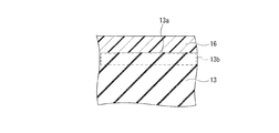
- the upper portion (surface layer portion) 13b (shown by the broken line) of the intermediate insulating film 13 on which the first polymerized film 16 shown in FIG. 6B is adsorbed is detached and removed.
- the surface of the intermediate insulating film 13 is oxidized and altered (modified) to form an oxygen-containing altered layer (modified layer) 15x.
- the thickness T3 of the altered layer 15x is about the same on the side surface and the bottom surface of the recess 13a of the intermediate insulating film 13.
- the thickness T3 of the altered layer 15x is, for example, about 3 nm to 10 nm, and can be appropriately set by adjusting the plasma energy (high frequency power) of the second gas. The higher the plasma energy of the second gas, the thicker the thickness T3 of the altered layer 15x, and the higher the oxygen concentration in the altered layer 15x.
- the upper insulating film 14 originally contains oxygen, it does not deteriorate like the intermediate insulating film 13.
- step S5 of FIG. 3 the exhaust unit 26 shown in FIG. 2 purges the inside of the processing container 21 to exhaust the second gas supplied in step S4.
- the inside of the processing container 21 may be evacuated, or a purge gas such as Ar gas may be supplied into the processing container 21.
- the gas supply unit 24 shown in FIG. 2 supplies the third gas into the processing container 21 to generate a plasma of the third gas.
- the third gas is composed of a fluorocarbon (C x Fy ) -based gas containing, for example, carbon and fluorine.
- the third gas includes carbon tetrafluoride (CF 4 ) gas, perfluorocyclobutane (C 4 F 8 ) gas, hexafluoro-1,3-butadiene (C 4 F 6 ) gas, and octafluoro. Cyclopentene (C 5 F 8 ) gas and the like can be mentioned.
- a rare gas such as argon (Ar) or an inert gas composed of nitrogen (N 2 ) may be supplied into the treatment container 21 and appropriately diluted.
- the pressure in the processing container 21 is about 20 to 30 mTorr
- the power of the upper electrode 22 is about 400 to 600 W
- the high frequency voltage is 0 V
- the CF is the third gas.
- the flow rate of the system gas is set to about 5 to 20 sccm
- the flow rate of Ar gas is set to about 400 to 600 sccm
- the processing time is set to about 5 to 15 seconds.
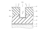
- the second polymerized film 17 is adsorbed on the surface of the altered layer 15 by the ions and radicals contained in the plasma of the third gas.
- the second polymerized film 17 is made of a CF-based polymer containing carbon (C) and fluorine (F).
- step S7 of FIG. 3 the exhaust unit 26 shown in FIG. 2 purges the inside of the processing container 21 to exhaust the third gas supplied in step S6.
- the inside of the processing container 21 may be evacuated, or a purge gas such as Ar gas may be supplied into the processing container 21.
- the fourth gas is supplied into the processing container 21 by the gas supply unit 24 shown in FIG. 2, and plasma of the fourth gas is generated.
- the fourth gas is a gas containing a rare gas.
- Specific examples of the fourth gas include helium (He), neon (Ne), argon (Ar), krypton (Kr), xenon (Xe) and the like.
- the pressure in the processing container 21 is about 20 to 30 mTorr
- the power of the upper electrode 22 is about 300 to 400 W
- the high frequency voltage is 70 V
- Ar which is the fourth gas.
- the gas flow rate is set to about 400 to 500 sccm
- the processing time is set to about 20 to 40 seconds.
- the altered layer 15x is desorbed and removed together with the second polymerized film 17 by the ions of the noble gas contained in the plasma of the fourth gas.
- the altered layer 15x on the bottom surface of the recess 13a of the intermediate insulating film 13 is substantially completely removed, so that the intermediate insulating film 13 is removed.
- the side surface of the recess 13a of the intermediate insulating film 13 is thinly removed because the penetration of Ar ions is shallower than that of the bottom surface of the recess 13a. Therefore, the altered layer 15x at the deep side surface of the recess 13a remains.
- step S9 of FIG. 3 the exhaust unit 26 shown in FIG. 2 purges the inside of the processing container 21 to exhaust the fourth gas supplied in step S8.
- the inside of the processing container 21 may be evacuated, or a purge gas such as Ar gas may be supplied into the processing container 21.
- step S10 of FIG. 3 the procedure of steps S2 to S9 is regarded as one cycle, and it is determined whether or not this cycle is repeated a predetermined number of times.
- the predetermined number of times can be set in advance as, for example, the number of times to achieve a predetermined etching amount. It should be noted that the predetermined number of times is once, and the steps S2 to S9 need not be repeated. If it has not been repeated a predetermined number of times, the procedure returns to step S2, and the cycles of steps S2 to S9 are repeated. In each cycle, the same process conditions may be set, or different process conditions may be set.
- the depth of the recess 13a of the intermediate insulating film 13 becomes deeper.
- the thickness of the altered layer 15x on the side surface of the recess 13a of the intermediate insulating film 13 increases with each plasma generation of the second gas in step S4 in each cycle. Therefore, a step of the altered layer 15x is formed one step at a time for each cycle.
- step S10 of FIG. 3 When the cycle of steps S2 to S9 is repeated a predetermined number of times in step S10 of FIG. 3, the polymer, natural oxide film, etc. are removed using dilute hydrofluoric acid (DHF) or the like, and the etching step is completed.
- DHF dilute hydrofluoric acid
- the intermediate insulating film 13 and the lower insulating film 12 are removed, openings (contact holes) are formed in the intermediate insulating film 13 and the lower insulating film 12, and the upper surface of the semiconductor layer 11 is formed. Part of is exposed.
- the thickness T1 of the altered layer 15 in the circumferential direction becomes thinner as it is closer to the semiconductor layer 11, and the outer peripheral surface of the altered layer 15 has a stepped shape.
- the conductive layer 18 is embedded in the openings (contact holes) of the lower insulating film 12, the intermediate insulating film 13, and the upper insulating film 14 by using a chemical vapor deposition (CVD) method or the like, as shown in FIG. It becomes a semiconductor device.
- CVD chemical vapor deposition
- the conductive layer 18 may be embedded in the openings (contact holes) of the lower insulating film 12 and the intermediate insulating film 13.
- an atomic layer in which the intermediate insulating film 13 made of Si 3 N 4 is targeted for etching and plasma generation and purging are repeated at least four times in the steps S2 to S9.
- the intermediate insulating film 13 can be removed for each atomic layer by etching (ALE). As a result, a high selectivity with the semiconductor layer 11 becomes possible, and low damage processing becomes possible.
- the left side of the graph in FIG. 10 shows the result of an argon (Ar) ion intrusion simulation when the power of the upper electrode 22 is set to 30 W (18 eV) and the treatment is performed for 60 seconds using ALE.
- the solid line profile in FIG. 10 shows the distribution of Ar ions, and the profile converted into continuous values is shown by the alternate long and short dash line.
- the right side of the graph in FIG. 10 shows the composition in the depth direction from the Si surface measured using an ellipsometer. From FIG. 10, it can be seen that the penetration depth of Ar ions into Si is 5 nm or less, and the recess amount of Si and the thickness of the altered layer 15 are 5 nm or less.
- the etching method according to the first comparative example will be described.
- the semiconductor layer 11, the lower insulating film 12 provided on the semiconductor layer 11, and the intermediate insulating film 13 provided on the lower insulating film 12 are used.
- a semiconductor wafer having an upper insulating film 14 provided on the intermediate insulating film 13 is prepared.
- a part of the upper insulating film 14 is selectively removed by using a photolithography technique and an etching technique to form an opening.
- the intermediate insulating film 13 and the lower insulating film 12 are removed by reactive ion etching (RIE) using the upper insulating film 14 as an etching mask.
- RIE reactive ion etching
- the oxide layer 11a on the upper part of the semiconductor layer 11 is removed to form a recess 11b, and further, a residual defect of Si is formed at the bottom of the recess 11b. 11c is generated.
- the dark current increases due to the formation of the recess 11b and the generation of the residual defect 11c.
- the slit 12a is formed in the lower insulating film 12 in the lateral direction, there is a concern that the yield may be deteriorated or the metal may be poorly embedded.
- the etching method of the semiconductor device according to the first embodiment even if the formation of the recesses of the semiconductor layer 11 due to overetching is suppressed or the recesses are formed.
- the depth of the recesses of the semiconductor layer 11 can be made shallower (for example, about 5 nm or less) than the recesses 11b of the first comparative example. Further, since the residual defect at the bottom of the recess of the semiconductor layer 11 can be suppressed or reduced, the dark current can be reduced. Further, as shown in FIG. 10, since the formation of the slit in the lateral direction of the lower insulating film 12 can be suppressed, the yield can be improved and the metal embedding defect can be suppressed.
- the etching method according to the second comparative example will be described.
- the semiconductor layer 11, the lower insulating film 12 provided on the semiconductor layer 11, and the lower insulating film 12 are covered with the same as in the first comparative example.
- a semiconductor wafer including the provided intermediate insulating film 13 and the upper insulating film 14 provided on the intermediate insulating film 13 is prepared.
- a part of the upper insulating film 14 is selectively removed by using a photolithography technique and an etching technique to form an opening.
- a recess 13a having a predetermined depth is formed in the intermediate insulating film 13.
- a procedure of generating a plasma of CH x Ph system gas and adsorbing the first polymerization film 16 and, as shown in FIG. 16, a plasma of Ar gas is generated to generate an intermediate insulating film.
- the procedure of removing 13 is repeated as one cycle. In this case, as shown in FIG. 16, a part of the first polymerized film 16 may remain when the Ar gas plasma is generated. Therefore, when the procedure shown in FIGS. 15 and 16 is repeated, the film thickness of the first polymerized film 16 becomes thicker, and it may be difficult to remove the intermediate insulating film 13.
- the etching method of the semiconductor device according to the first embodiment by repeating the procedure of steps S2 to S9 shown in FIG. 3, the first polymer film 16 does not remain and the intermediate insulating film is formed. 13 can be easily removed.
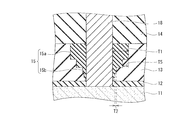
- the semiconductor device according to the second embodiment is different from the semiconductor device according to the first embodiment shown in FIG. 1 in that the outer peripheral surface of the altered layer 15 has a substantially curved surface (tapered shape). ..
- the step-shaped step on the outer peripheral surface of the altered layer 15 is shallow and minutely formed, the step is continuously connected and is regarded as a substantially curved surface. be able to.
- the circumferential thickness T1 of the altered layer 15 becomes thinner as it approaches the semiconductor layer 11. Since other configurations of the semiconductor device according to the second embodiment are the same as those of the semiconductor device according to the first embodiment shown in FIG. 1, duplicate description will be omitted.
- the etching method of the semiconductor device according to the second embodiment is the same as the etching method of the semiconductor device according to the first embodiment, and the second gas is generated at the time of generating the plasma of the second gas in step S4 shown in FIG.
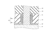
- the shape of the altered layer 15 of the semiconductor device according to the third embodiment is different from that of the semiconductor device according to the first embodiment shown in FIG.
- the outer peripheral surface of the upper portion 15a of the altered layer 15 is substantially vertical, and the thickness T1 of the upper portion 15a of the altered layer 15 in the circumferential direction is substantially constant.
- the outer peripheral surface of the lower portion 15b of the alteration layer 15 has a stepped shape, and the thickness T1 of the lower portion 15b of the alteration layer 15 in the circumferential direction becomes thinner as it approaches the semiconductor layer 11. Since other configurations of the semiconductor device according to the third embodiment are the same as those of the semiconductor device according to the first embodiment shown in FIG. 1, duplicate description will be omitted.
- the intermediate insulating film 13 on the bottom surface of the recess 13a is removed by a predetermined depth by dry etching such as RIE.
- the procedure of steps S2 to S9 shown in FIG. 3 is repeated.
- the outer peripheral surface of the upper portion 15a of the altered layer 15 corresponding to the position where the intermediate insulating film 13 is removed by dry etching such as RIE becomes substantially vertical.
- the steps S2 to S9 shown in FIG. 3 the outer peripheral surface of the lower portion 15b of the altered layer 15 corresponding to the position where the intermediate insulating film 13 is removed becomes a stepped shape.
- the number of repetitions of the steps S2 to S9 can be reduced by using normal dry etching in the first half of the etching process of the intermediate insulating film 13.
- the formation of the recesses in the semiconductor layer 11 can be suppressed or the depth of the recesses can be reduced by repeating the steps S2 to S9.
- the plasma of the second gas is generated at the time of generating the plasma of the second gas in step S4 shown in FIG.
- the case of increasing the energy is illustrated.
- the alteration layer 15x is compared with the circumferential thickness T3 of the alteration layer 15x shown in FIG. 7A.
- the thickness T4 in the circumferential direction becomes thicker.
- the outer peripheral surface of the alteration layer 15 has a stepped shape, and the thickness T1 in the circumferential direction of the alteration layer 15 becomes thinner as it approaches the semiconductor layer 11. This point is common to the semiconductor device according to the first embodiment shown in FIG. However, in the semiconductor device according to the fourth embodiment, the step-shaped step T5 on the outer peripheral surface of the altered layer 15 is larger than the step T2 of the semiconductor device according to the first embodiment shown in FIG. Since other configurations of the semiconductor device according to the fourth embodiment are the same as those of the semiconductor device according to the first embodiment shown in FIG. 1, duplicate description will be omitted.
- step S4 As a method of etching the semiconductor device according to the fourth embodiment, in the etching method of the semiconductor device according to the first embodiment, when the procedure of steps S2 to S9 shown in FIG. 3 is repeated, in step S4, FIG. As shown, the plasma energy of the second gas may be increased.
- the etching amount in one cycle of the procedure of steps S2 to S9 shown in FIG. 3 can be increased, and the etching amount of steps S2 to S9 shown in FIG. 3 can be increased.
- the number of times the procedure is repeated can be reduced.
- the shape of the upper portion 15a of the alteration layer 15 of the semiconductor device according to the fifth embodiment is different from that of the semiconductor device according to the first embodiment shown in FIG.
- the outer peripheral surface of the upper portion 15a of the altered layer 15 has a staircase shape, and the thickness T5 of the staircase-shaped step is substantially constant.
- the outer peripheral surface of the lower portion 15b of the alteration layer 15 is also stepped, but the step thickness T2 of the step shape is thinner than the step thickness T5 of the upper portion 15a of the alteration layer 15. Since other configurations of the semiconductor device according to the fifth embodiment are the same as those of the semiconductor device according to the first embodiment shown in FIG. 1, duplicate description will be omitted.
- steps S2 to S9 shown in FIG. In the first half of the plurality of cycles of the procedure, the plasma energy of the second gas in step S4 is relatively increased. After that, in the latter half of the plurality of cycles of the procedure of steps S2 to S9 shown in FIG. 3, the plasma energy of the second gas in step S4 is relatively reduced.
- the etching amount in one cycle in the first half of the plurality of cycles, can be increased and the number of cycle repetitions can be reduced.
- the etching amount in one cycle in the latter half of the plurality of cycles, can be reduced to improve the etching accuracy, and the formation of the recesses in the semiconductor layer 11 can be suppressed or the depth of the recesses can be reduced. ..
- the shape of the upper portion 15a and the lower portion 15b of the alteration layer 15 of the semiconductor device according to the sixth embodiment is different from that of the semiconductor device according to the first embodiment shown in FIG.
- the outer peripheral surface of the upper portion 15a of the altered layer 15 is substantially vertical, and the thickness T1 of the upper portion 15a of the altered layer 15 in the circumferential direction is substantially constant.
- the outer peripheral surface of the lower portion 15b of the altered layer 15 is stepped.
- the step-shaped step of the lower portion 15b of the altered layer 15 is one step, but it may be a plurality of steps. Since other configurations of the semiconductor device according to the sixth embodiment are the same as those of the semiconductor device according to the first embodiment shown in FIG. 1, duplicate description will be omitted.
- etching the semiconductor device according to the sixth embodiment in the etching method for the semiconductor device according to the first embodiment, after forming a recess 13a in the intermediate insulating film 13 as shown in FIG. 5, dry etching such as RIE or the like is performed. As a result, the intermediate insulating film 13 on the bottom surface of the recess 13a is removed by a predetermined depth. After that, the procedure of steps S2 to S9 shown in FIG. 3 is repeated, but the plasma energy of the second gas in step S4 is made larger than the etching method of the semiconductor device according to the first embodiment. As a result, as shown in FIG.
- the outer peripheral surface of the upper portion 15a of the altered layer 15 corresponding to the position where the intermediate insulating film 13 is removed by dry etching such as RIE becomes substantially vertical.
- the outer peripheral surface of the lower portion 15b of the altered layer 15 corresponding to the position where the intermediate insulating film 13 is removed becomes a stepped shape.
- the number of repetitions of the steps S2 to S9 can be reduced by using normal dry etching in the first half of the etching step of the intermediate insulating film 13.
- the formation of the recesses in the semiconductor layer 11 can be suppressed or the depth of the recesses can be reduced by repeating the steps S2 to S9.
- the solid-state image sensor and the electronic device to which the semiconductor devices of the first to sixth embodiments can be applied will be exemplified.
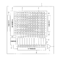
- the solid-state image sensor according to the seventh embodiment has a pixel region (imaging region) 3 in which pixels 2 are arranged in a matrix and a peripheral circuit that processes a pixel signal output from the pixel region 3. It is provided with parts (4,5,6,7,8).
- Pixel 2 generally has a photoelectric conversion region composed of a photodiode that photoelectrically converts incident light, and a plurality of pixel transistors for reading out signal charges generated by photoelectric conversion in the photoelectric conversion region.
- the plurality of pixel transistors can be composed of, for example, three transistors, a transfer transistor, a reset transistor, and an amplification transistor.
- the plurality of pixel transistors may be composed of four transistors by further adding a selection transistor.
- the peripheral circuit unit (4,5,6,7,8) has a vertical drive circuit 4, a column signal processing circuit 5, a horizontal drive circuit 6, an output circuit 7, and a control circuit 8.
- the control circuit 8 receives the input clock and data instructing the operation mode and the like, and outputs data such as internal information of the solid-state image sensor. For example, the control circuit 8 generates a clock signal or a control signal that serves as a reference for the operation of the vertical drive circuit 4, the column signal processing circuit 5, the horizontal drive circuit 6, etc., based on the vertical synchronization signal, the horizontal synchronization signal, and the master clock. do.
- the control circuit 8 outputs the generated clock signal and control signal to the vertical drive circuit 4, the column signal processing circuit 5, the horizontal drive circuit 6, and the like.
- the vertical drive circuit 4 is composed of, for example, a shift register.
- the vertical drive circuit 4 selects the pixel drive wiring, supplies a pulse for driving the pixel 2 to the selected pixel drive wiring, and drives the pixel 2 in units of rows.
- the vertical drive circuit 4 selectively scans each pixel 2 of the pixel region 3 in a row-by-row manner in the vertical direction, and passes through the vertical signal line 9 to become a photoelectric conversion region of each pixel 2, for example, in a photodiode, depending on the amount of light received.
- a pixel signal based on the generated signal charge is supplied to the column signal processing circuit 5.
- the column signal processing circuit 5 is arranged for each column of pixels 2, for example.
- the column signal processing circuit 5 performs signal processing such as noise removal for each pixel string of the signal output from the pixel 2 for one row.
- the column signal processing circuit 5 performs signal processing such as CDS for removing fixed pattern noise peculiar to pixel 2, signal amplification, and AD conversion.
- a horizontal selection switch (not shown) is provided in the output stage of the column signal processing circuit 5 so as to be connected to the horizontal signal line 10.
- the horizontal drive circuit 6 is composed of, for example, a shift register.
- the horizontal drive circuit 6 sequentially outputs horizontal scanning pulses to sequentially select each of the column signal processing circuits 5, and causes each of the column signal processing circuits 5 to output pixel signals to the horizontal signal line 10.
- the output circuit 7 performs signal processing on the signals sequentially supplied from each of the column signal processing circuits 5 through the horizontal signal line 10 and outputs the signals.
- the output circuit 7 may perform only buffering, black level adjustment, column variation correction, various digital signal processing, and the like.
- the input / output terminal 31 exchanges signals with the outside.
- the pixel region 3 and the peripheral circuit portions (4,5,6,7,8) of the solid-state image sensor according to the seventh embodiment are formed on one substrate 1, but a plurality of substrates are formed. It may be formed by a laminated structure in which they are bonded together.
- the solid-state image sensor according to the seventh embodiment is composed of the first and second substrates, a photoelectric conversion region and a pixel transistor are provided on the first substrate, and peripheral circuits (3, 4, 5, 6) are provided on the second substrate. , 7) and the like may be provided.
- the first substrate may be provided with a photoelectric conversion region and a part of the pixel transistors
- the second substrate may be provided with a part of the remainder of the pixel transistors and peripheral circuits (3, 4, 5, 6, 7) and the like. ..
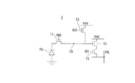
- FIG. 24 shows an example of an equivalent circuit of pixel 2 of the solid-state image sensor according to the seventh embodiment.
- the anode of the photodiode PD which is the photoelectric conversion region of the pixel 2
- the source of the transfer transistor T1 which is an active element is connected to the cathode of the photodiode PD.
- a floating diffusion region (floating diffusion region) FD is connected to the drain of the transfer transistor T1.
- the floating diffusion region FD is connected to the source of the reset transistor T2, which is an active element, and the gate of the amplification transistor T3, which is an active element.
- the source of the amplification transistor T3 is connected to the drain of the selection transistor T4 which is an active element, and the drain of the amplification transistor T3 is connected to the power supply Vdd.
- the source of the selection transistor T4 is connected to the vertical signal line VSL.
- the drain of the reset transistor T2 is connected to the power supply Vdd.
- the control potential TRG is applied to the transfer transistor T1, and the signal charge generated by the photodiode PD is transferred to the floating diffusion region FD.
- the signal charge transferred to the floating diffusion region FD is read out and applied to the gate of the amplification transistor T3.
- a horizontal line selection signal SEL is given to the gate of the selection transistor T4 from the vertical shift register.
- the selection signal SEL By setting the selection signal SEL to a high (H) level, the selection transistor T4 becomes conductive, and a current corresponding to the potential of the floating diffusion region FD amplified by the amplification transistor T3 flows in the vertical signal line VSL.
- the reset signal RST applied to the gate of the reset transistor T2 to a high (H) level, the reset transistor T2 becomes conductive and the signal charge accumulated in the floating diffusion region FD is reset.
- the semiconductor device is a conductive layer embedded in a contact hole such as a photodiode PD, a transfer transistor T1, a reset transistor T2, an amplification transistor T3, and a selection transistor T4 shown in FIG. 24. It may be a semiconductor device having a semiconductor layer (diffusion layer) connected to (contact).
- FIG. 25 is a block diagram showing a configuration example of an embodiment of an imaging device as an electronic device to which the present disclosure is applied.
- the image pickup device 1000 of FIG. 25 is a video camera, a digital still camera, or the like.
- the image pickup device 1000 includes a lens group 1001, a solid-state image sensor 1002, a DSP circuit 1003, a frame memory 1004, a display unit 1005, a recording unit 1006, an operation unit 1007, and a power supply unit 1008.
- the DSP circuit 1003, the frame memory 1004, the display unit 1005, the recording unit 1006, the operation unit 1007, and the power supply unit 1008 are connected to each other via the bus line 1009.
- the lens group 1001 captures incident light (image light) from the subject and forms an image on the image pickup surface of the solid-state image pickup device 1002.
- the solid-state image sensor 1002 corresponds to the solid-state image sensor according to the seventh embodiment of the CMOS image sensor described above.
- the solid-state image sensor 1002 converts the amount of incident light imaged on the imaging surface by the lens group 1001 into an electric signal in pixel units and supplies it to the DSP circuit 1003 as a pixel signal.
- the DSP circuit 1003 performs predetermined image processing on the pixel signal supplied from the solid-state image sensor 1002, supplies the image signal after the image processing to the frame memory 1004 in frame units, and temporarily stores the image signal.
- the display unit 1005 is composed of a panel-type display device such as a liquid crystal panel or an organic EL (Electro Luminescence) panel, and displays an image based on a frame-based pixel signal temporarily stored in the frame memory 1004.
- a panel-type display device such as a liquid crystal panel or an organic EL (Electro Luminescence) panel, and displays an image based on a frame-based pixel signal temporarily stored in the frame memory 1004.
- the recording unit 1006 is composed of a DVD (Digital Versatile Disk), a flash memory, etc., and reads and records a frame-by-frame pixel signal temporarily stored in the frame memory 1004.
- DVD Digital Versatile Disk
- flash memory etc.
- the operation unit 1007 issues operation commands for various functions of the image pickup apparatus 1000 under the operation of the user.
- the power supply unit 1008 supplies power to the DSP circuit 1003, the frame memory 1004, the display unit 1005, the recording unit 1006, and the operation unit 1007 as appropriate.
- the electronic device to which this technology is applied may be any device that uses a CMOS image sensor for the image acquisition unit (photoelectric conversion unit), and in addition to the image pickup device 1000, a portable terminal device having an image pickup function, and a CMOS image for the image reading unit.
- CMOS image sensor for the image acquisition unit (photoelectric conversion unit)
- the image pickup device 1000 a portable terminal device having an image pickup function
- CMOS image for the image reading unit.
- copiers and the like that use sensors.
- application examples of the present disclosure include an infrared light receiving element, an image pickup device using the infrared light receiving element, an electronic device, and the like, and the applications include not only ordinary cameras and smartphones, but also industrial devices such as surveillance cameras and factory inspections.
- a wide range of applications for imaging and sensing are conceivable, such as cameras for cameras, in-vehicle cameras, ranging sensors (ToF sensors), and infrared sensors. An example thereof will be described below.
- the present technology can have the following configurations.
- (3) The side surface of the altered layer in contact with the first insulating film has a stepped shape.
- the step-shaped step at the bottom of the altered layer is smaller than the step-shaped step at the top of the semiconductor layer.
- the relative permittivity of the altered layer is lower than the relative permittivity of the first insulating film.
- the first insulating film is made of silicon nitride.
- the altered layer contains silicon oxide or silicon oxynitride.
- a second insulating film provided between the semiconductor layer and the first insulating film is further provided.
- the second insulating film is made of silicon oxide.
- the semiconductor device according to (8) above. (10) A third insulating film provided on the first insulating film is further provided.
- the third insulating film is made of a silicon oxide film.
- the semiconductor device according to (10) above. (12)
- the first polymer film is adsorbed on the insulating film provided on the semiconductor layer containing silicon by the plasma of the first gas.
- the first polymer film was removed by the plasma of the second gas, and the upper surface of the insulating film exposed by removing the first polymer film was oxidized to form an altered layer.
- the second polymer film is adsorbed on the altered layer by the plasma of the third gas.
- the second polymerized film and the altered layer are removed by the plasma of the fourth gas.
- Etching methods including that.
- the first gas contains carbon, hydrogen and fluorine.
- the second gas contains oxygen.
- the third gas contains carbon and fluorine.
- the fourth gas contains a noble gas.
- the cycle including adsorbing the first polymer film, forming the altered layer, adsorbing the second polymer film, and removing the altered layer is repeated a plurality of times.
- (19) The plasma energy of the second gas in each of the plurality of cycles is the same.
- (20) The plasma energy of the second gas in the second half of the plurality of times is made smaller than the plasma energy of the second gas in the cycle of the first half of the plurality of times.
Landscapes
- Drying Of Semiconductors (AREA)
- Internal Circuitry In Semiconductor Integrated Circuit Devices (AREA)
Abstract
Description
<半導体装置の構造>
第1実施形態に係る半導体装置は、図1に示すように、シリコン(Si)を含む半導体層11と、半導体層11上に設けられた絶縁膜(下層絶縁膜)12と、下層絶縁膜12上に設けられた絶縁膜(中間絶縁膜)13と、中間絶縁膜13上に設けられた絶縁膜(上層絶縁膜)14とを備える。
次に、後述する第1実施形態に係る半導体装置のエッチング方法を実施するための、第1実施形態に係るエッチング装置(プラズマ処理装置)の概略構成を説明する。第1実施形態に係るプラズマ処理装置は、図2に示すように、被処理体100を収容する処理容器21を備える。
次に、図3のフローチャート及び図4~図10の工程断面図を参照して、第1実施形態に係る半導体装置のエッチング方法を説明する。図6A及び図6Bは同一工程を示しており、図6Aの破線で囲んだ部分Aの拡大図が図6Bである。図7A及び図7B、図8A及び図8B、図9A及び図9Bも、図6A及び図6Bと同様の関係である。
次に、第1比較例に係るエッチング方法を説明する。第1比較例に係るエッチング方法では、図12に示すように、半導体層11と、半導体層11上に設けられた下層絶縁膜12と、下層絶縁膜12上に設けられた中間絶縁膜13と、中間絶縁膜13上に設けられた上層絶縁膜14を備える半導体ウェハを準備する。そして、フォトリソグラフィ技術及びエッチング技術を用いて、上層絶縁膜14の一部が選択的に除去され、開口部が形成されている。
次に、第2比較例に係るエッチング方法を説明する。第2比較例に係るエッチング方法では、第1比較例と同様に、図12に示すように、半導体層11と、半導体層11上に設けられた下層絶縁膜12と、下層絶縁膜12上に設けられた中間絶縁膜13と、中間絶縁膜13上に設けられた上層絶縁膜14を備える半導体ウェハを準備する。そして、フォトリソグラフィ技術及びエッチング技術を用いて、上層絶縁膜14の一部が選択的に除去され、開口部が形成されている。
第2実施形態に係る半導体装置は、図17に示すように、変質層15の外周面が略曲面(テーパ形状)であることが、図1に示した第1実施形態に係る半導体装置と異なる。図1に示した第1実施形態に係る半導体装置と比較して、変質層15の外周面の階段形状の段差が浅く微小に形成されているため、段差が連続的に繋がり、略曲面と見なすことができる。変質層15の周方向の厚さT1は、半導体層11に近いほど薄くなっている。第2実施形態に係る半導体装置の他の構成は、図1に示した第1実施形態に係る半導体装置と同様であるので、重複した説明を省略する。
第3実施形態に係る半導体装置は、図18に示すように、変質層15の形状が、図1に示した第1実施形態に係る半導体装置と異なる。変質層15の上部15aの外周面は略垂直であり、変質層15の上部15aの周方向の厚さT1は略一定である。変質層15の下部15bの外周面は階段形状であり、変質層15の下部15bの周方向の厚さT1は、半導体層11に近いほど薄くなっている。第3実施形態に係る半導体装置の他の構成は、図1に示した第1実施形態に係る半導体装置と同様であるので、重複した説明を省略する。
以下の第4~第6実施形態においては、第1実施形態に係る半導体装置のエッチング方法と比較して、図3に示したステップS4の第2ガスのプラズマの生成時に、第2ガスのプラズマエネルギーを大きくする場合を例示する。例えば、図3に示したステップS4の第2ガスのプラズマエネルギーを大きくすると、図7Aに示した変質層15xの周方向の厚さT3と比較して、図19に示すように、変質層15xの周方向の厚さT4が厚くなる。
第5実施形態に係る半導体装置は、図21に示すように、変質層15の上部15aの形状が、図1に示した第1実施形態に係る半導体装置と異なる。変質層15の上部15aの外周面は階段形状であり、階段形状の段差の厚さT5は略一定である。一方、変質層15の下部15bの外周面も階段形状であるが、階段形状の段差の厚さT2は、変質層15の上部15aの段差の厚さT5よりも薄い。第5実施形態に係る半導体装置の他の構成は、図1に示した第1実施形態に係る半導体装置と同様であるので、重複した説明を省略する。
第6実施形態に係る半導体装置は、図22に示すように、変質層15の上部15a及び下部15bの形状が、図1に示した第1実施形態に係る半導体装置と異なる。変質層15の上部15aの外周面は略垂直であり、変質層15の上部15aの周方向の厚さT1は略一定である。変質層15の下部15bの外周面は階段形状である。なお、図22では、変質層15の下部15bの階段形状の段差は1段であるが、複数段であってよい。第6実施形態に係る半導体装置の他の構成は、図1に示した第1実施形態に係る半導体装置と同様であるので、重複した説明を省略する。
第7実施形態では、第1~第6実施形態の半導体装置を適用可能な固体撮像装置及び電子機器について例示する。
第7実施形態に係る固体撮像装置として、CMOS(Complementary Metal Oxide Semiconductor)イメージセンサを一例として説明する。第7実施形態に係る固体撮像装置は、図23に示すように、画素2が行列状に配列された画素領域(撮像領域)3と、画素領域3から出力された画素信号を処理する周辺回路部(4,5,6,7,8)とを備える。
図25は、本開示を適用した電子機器としての撮像装置の一実施の形態の構成例を示すブロック図である。図25の撮像装置1000は、ビデオカメラやデジタルスチルカメラ等である。撮像装置1000は、レンズ群1001、固体撮像素子1002、DSP回路1003、フレームメモリ1004、表示部1005、記録部1006、操作部1007、および電源部1008からなる。DSP回路1003、フレームメモリ1004、表示部1005、記録部1006、操作部1007、および電源部1008は、バスライン1009を介して相互に接続されている。
上記のように、本技術は第1~第7実施形態によって記載したが、この開示の一部をなす論述及び図面は本技術を限定するものであると理解すべきではない。上記の実施形態が開示する技術内容の趣旨を理解すれば、当業者には様々な代替実施形態、実施例及び運用技術が本技術に含まれ得ることが明らかとなろう。また、第1~第7実施形態がそれぞれ開示する構成を、矛盾の生じない範囲で適宜組み合わせることができる。
(1)
シリコンを含む半導体層と、
前記半導体層上に設けられ、前記半導体層の一部を露出する開口部を有する第1絶縁膜と、
前記第1絶縁膜の前記開口部に埋め込まれ、前記半導体層に下端が接する導電層と、
前記第1絶縁膜と前記導電層との間に設けられ、酸素を含む変質層と、
を備える、半導体装置。
(2)
前記変質層は、前記半導体層に近いほど前記第1絶縁膜と前記導電層に挟まれた厚さが薄くなる、
前記(1)に記載の半導体装置。
(3)
前記変質層の前記第1絶縁膜と接する側面が階段形状を有する、
前記(2)に記載の半導体装置。
(4)
前記変質層の下部の前記階段形状の段差が、前記半導体層の上部の前記階段形状の段差よりも小さい、
前記(3)に記載の半導体装置。
(5)
前記変質層の比誘電率は、前記第1絶縁膜の比誘電率よりも低い、
前記(1)~(4)のいずれか1つに記載の半導体装置。
(6)
前記第1絶縁膜は、窒化珪素からなる、
前記(1)~(5)のいずれか1つに記載の半導体装置。
(7)
前記変質層は、酸化珪素又は酸窒化珪素を含む、
前記(1)~(6)のいずれか1つに記載の半導体装置。
(8)
前記半導体層と前記第1絶縁膜との間に設けられた第2絶縁膜を更に備える、
前記(1)~(7)のいずれか1つに記載の半導体装置。
(9)
前記第2絶縁膜は、酸化珪素からなる、
前記(8)に記載の半導体装置。
(10)
前記第1絶縁膜上に設けられた第3絶縁膜を更に備える、
前記(1)~(9)のいずれか1つに記載の半導体装置。
(11)
前記第3絶縁膜は、酸化珪素膜からなる、
前記(10)に記載の半導体装置。
(12)
第1ガスのプラズマにより、シリコンを含む半導体層上に設けられた絶縁膜上に第1重合膜を吸着させ、
第2ガスのプラズマにより、前記第1重合膜を除去し、前記第1重合膜が除去されて露出した前記絶縁膜の上面を酸化して変質層を形成し、
第3ガスのプラズマにより、前記変質層上に第2重合膜を吸着させ、
第4ガスのプラズマにより、前記第2重合膜及び前記変質層を除去する、
ことを含む、エッチング方法。
(13)
前記第1ガスは、炭素、水素及びフッ素を含有する、
前記(12)に記載のエッチング方法。
(14)
前記第2ガスは、酸素を含有する、
前記(12)又は(13)に記載のエッチング方法。
(15)
前記第3ガスは、炭素及びフッ素を含有する。
前記(12)~(14)のいずれか1つに記載のエッチング方法。
(16)
前記第4ガスは、希ガスを含有する、
前記(12)~(15)のいずれか1つに記載のエッチング方法。
(17)
前記第1重合膜を吸着させる前に、
ドライエッチングにより前記第1絶縁膜の上部を除去することを更に含む、
前記(12)~(16)のいずれか1つに記載のエッチング方法。
(18)
前記第1重合膜を吸着させ、前記変質層を形成し、前記第2重合膜を吸着させ、前記変質層を除去することを含むサイクルを複数回繰り返す、
前記(12)~(17)のいずれか1つに記載のエッチング方法。
(19)
前記複数回の各サイクルにおける前記第2ガスのプラズマエネルギーを同一とする、
前記(18)に記載のエッチング方法。
(20)
前記複数回の前半の前記サイクルにおける前記第2ガスのプラズマエネルギーよりも、前記複数回の後半の前記サイクルにおける前記第2ガスのプラズマエネルギーを小さくする、
前記(18)に記載のエッチング方法。
Claims (20)
- シリコンを含む半導体層と、
前記半導体層上に設けられ、前記半導体層の一部を露出する開口部を有する第1絶縁膜と、
前記第1絶縁膜の前記開口部に埋め込まれ、前記半導体層に下端が接する導電層と、
前記第1絶縁膜と前記導電層との間に設けられ、酸素を含む変質層と、
を備える、半導体装置。 - 前記変質層は、前記半導体層に近いほど前記第1絶縁膜と前記導電層に挟まれた厚さが薄くなる、
請求項1に記載の半導体装置。 - 前記変質層の前記第1絶縁膜と接する側面が階段形状を有する、
請求項2に記載の半導体装置。 - 前記変質層の下部の前記階段形状の段差が、前記半導体層の上部の前記階段形状の段差よりも小さい、
請求項3に記載の半導体装置。 - 前記変質層の比誘電率は、前記第1絶縁膜の比誘電率よりも低い、
請求項1に記載の半導体装置。 - 前記第1絶縁膜は、窒化珪素からなる、
請求項1に記載の半導体装置。 - 前記変質層は、酸化珪素又は酸窒化珪素を含む、
請求項1に記載の半導体装置。 - 前記半導体層と前記第1絶縁膜との間に設けられた第2絶縁膜を更に備える、
請求項1に記載の半導体装置。 - 前記第2絶縁膜は、酸化珪素からなる、
請求項8に記載の半導体装置。 - 前記第1絶縁膜上に設けられた第3絶縁膜を更に備える、
請求項1に記載の半導体装置。 - 前記第3絶縁膜は、酸化珪素膜からなる、
請求項10に記載の半導体装置。 - 第1ガスのプラズマにより、シリコンを含む半導体層上に設けられた絶縁膜上に第1重合膜を吸着させ、
第2ガスのプラズマにより、前記第1重合膜を除去し、前記第1重合膜が除去されて露出した前記絶縁膜の上面を酸化して変質層を形成し、
第3ガスのプラズマにより、前記変質層上に第2重合膜を吸着させ、
第4ガスのプラズマにより、前記第2重合膜及び前記変質層を除去する、
ことを含む、エッチング方法。 - 前記第1ガスは、炭素、水素及びフッ素を含有する、
請求項12に記載のエッチング方法。 - 前記第2ガスは、酸素を含有する、
請求項12に記載のエッチング方法。 - 前記第3ガスは、炭素及びフッ素を含有する。
請求項12に記載のエッチング方法。 - 前記第4ガスは、希ガスを含有する、
請求項12に記載のエッチング方法。 - 前記第1重合膜を吸着させる前に、
ドライエッチングにより前記第1絶縁膜の上部を除去することを更に含む、
請求項12に記載のエッチング方法。 - 前記第1重合膜を吸着させ、前記変質層を形成し、前記第2重合膜を吸着させ、前記変質層を除去することを含むサイクルを複数回繰り返す、
請求項12に記載のエッチング方法。 - 前記複数回の各サイクルにおける前記第2ガスのプラズマエネルギーを同一とする、
請求項18に記載のエッチング方法。 - 前記複数回の前半の前記サイクルにおける前記第2ガスのプラズマエネルギーよりも、前記複数回の後半の前記サイクルにおける前記第2ガスのプラズマエネルギーを小さくする、
請求項18に記載のエッチング方法。
Priority Applications (3)
| Application Number | Priority Date | Filing Date | Title |
|---|---|---|---|
| CN202080093564.8A CN114981933B (zh) | 2020-01-30 | 2020-06-15 | 半导体装置及蚀刻方法 |
| JP2021574440A JP7629875B2 (ja) | 2020-01-30 | 2020-06-15 | 半導体装置及びエッチング方法 |
| US17/793,333 US20220375763A1 (en) | 2020-01-30 | 2020-06-15 | Semiconductor device and etching method |
Applications Claiming Priority (2)
| Application Number | Priority Date | Filing Date | Title |
|---|---|---|---|
| US202062968016P | 2020-01-30 | 2020-01-30 | |
| US62/968016 | 2020-01-30 |
Publications (1)
| Publication Number | Publication Date |
|---|---|
| WO2021152879A1 true WO2021152879A1 (ja) | 2021-08-05 |
Family
ID=77079901
Family Applications (1)
| Application Number | Title | Priority Date | Filing Date |
|---|---|---|---|
| PCT/JP2020/023359 Ceased WO2021152879A1 (ja) | 2020-01-30 | 2020-06-15 | 半導体装置及びエッチング方法 |
Country Status (4)
| Country | Link |
|---|---|
| US (1) | US20220375763A1 (ja) |
| JP (1) | JP7629875B2 (ja) |
| CN (1) | CN114981933B (ja) |
| WO (1) | WO2021152879A1 (ja) |
Families Citing this family (2)
| Publication number | Priority date | Publication date | Assignee | Title |
|---|---|---|---|---|
| US11569127B2 (en) * | 2021-03-04 | 2023-01-31 | Taiwan Semiconductor Manufacturing Company Limited | Double patterning approach by direct metal etch |
| US20250232982A1 (en) * | 2024-01-16 | 2025-07-17 | Tokyo Electron Limited | Oxidation based atomic layer etching |
Citations (3)
| Publication number | Priority date | Publication date | Assignee | Title |
|---|---|---|---|---|
| JP2000183040A (ja) * | 1998-12-15 | 2000-06-30 | Canon Inc | 有機層間絶縁膜エッチング後のレジストアッシング方法 |
| JP2000243749A (ja) * | 1999-02-17 | 2000-09-08 | Matsushita Electric Ind Co Ltd | 絶縁膜の形成方法 |
| JP2014170764A (ja) * | 2012-04-27 | 2014-09-18 | Tokyo Electron Ltd | 成膜方法及び成膜装置 |
Family Cites Families (15)
| Publication number | Priority date | Publication date | Assignee | Title |
|---|---|---|---|---|
| TW387151B (en) * | 1998-02-07 | 2000-04-11 | United Microelectronics Corp | Field effect transistor structure of integrated circuit and the manufacturing method thereof |
| JP2002319551A (ja) * | 2001-04-23 | 2002-10-31 | Nec Corp | 半導体装置およびその製造方法 |
| US6498067B1 (en) * | 2002-05-02 | 2002-12-24 | Taiwan Semiconductor Manufacturing Company | Integrated approach for controlling top dielectric loss during spacer etching |
| CN1278409C (zh) * | 2002-06-10 | 2006-10-04 | 株式会社东芝 | 半导体器件的制造方法和半导体器件 |
| JP4207113B2 (ja) | 2002-06-26 | 2009-01-14 | パナソニック株式会社 | 配線構造の形成方法 |
| US6806126B1 (en) * | 2002-09-06 | 2004-10-19 | Advanced Micro Devices, Inc. | Method of manufacturing a semiconductor component |
| JP3676784B2 (ja) | 2003-01-28 | 2005-07-27 | Necエレクトロニクス株式会社 | 半導体装置およびその製造方法 |
| JP2004289046A (ja) * | 2003-03-25 | 2004-10-14 | Renesas Technology Corp | キャパシタを有する半導体装置の製造方法 |
| JP2005268312A (ja) * | 2004-03-16 | 2005-09-29 | Semiconductor Leading Edge Technologies Inc | レジスト除去方法及びそれを用いて製造した半導体装置 |
| JP2007019393A (ja) * | 2005-07-11 | 2007-01-25 | Toshiba Matsushita Display Technology Co Ltd | 薄膜トランジスタ及びその製造方法 |
| JP2011077468A (ja) | 2009-10-02 | 2011-04-14 | Panasonic Corp | 半導体装置の製造方法および半導体装置 |
| KR102067051B1 (ko) * | 2011-10-24 | 2020-01-16 | 가부시키가이샤 한도오따이 에네루기 켄큐쇼 | 반도체 장치 및 반도체 장치의 제작 방법 |
| JP2014225501A (ja) * | 2013-05-15 | 2014-12-04 | 東京エレクトロン株式会社 | プラズマエッチング方法及びプラズマエッチング装置 |
| US10781519B2 (en) * | 2018-06-18 | 2020-09-22 | Tokyo Electron Limited | Method and apparatus for processing substrate |
| CN112640064A (zh) * | 2018-08-24 | 2021-04-09 | 朗姆研究公司 | 用于高深宽比蚀刻的含金属钝化 |
-
2020
- 2020-06-15 JP JP2021574440A patent/JP7629875B2/ja active Active
- 2020-06-15 WO PCT/JP2020/023359 patent/WO2021152879A1/ja not_active Ceased
- 2020-06-15 US US17/793,333 patent/US20220375763A1/en not_active Abandoned
- 2020-06-15 CN CN202080093564.8A patent/CN114981933B/zh active Active
Patent Citations (3)
| Publication number | Priority date | Publication date | Assignee | Title |
|---|---|---|---|---|
| JP2000183040A (ja) * | 1998-12-15 | 2000-06-30 | Canon Inc | 有機層間絶縁膜エッチング後のレジストアッシング方法 |
| JP2000243749A (ja) * | 1999-02-17 | 2000-09-08 | Matsushita Electric Ind Co Ltd | 絶縁膜の形成方法 |
| JP2014170764A (ja) * | 2012-04-27 | 2014-09-18 | Tokyo Electron Ltd | 成膜方法及び成膜装置 |
Also Published As
| Publication number | Publication date |
|---|---|
| CN114981933A (zh) | 2022-08-30 |
| JPWO2021152879A1 (ja) | 2021-08-05 |
| CN114981933B (zh) | 2025-06-10 |
| US20220375763A1 (en) | 2022-11-24 |
| JP7629875B2 (ja) | 2025-02-14 |
Similar Documents
| Publication | Publication Date | Title |
|---|---|---|
| US9087757B2 (en) | Semiconductor device, solid-state imaging device, method for manufacturing semiconductor device, method for manufacturing solid-state imaging device, and electronic apparatus | |
| KR101952072B1 (ko) | 전계 효과형 트랜지스터, 전계 효과형 트랜지스터의 제조 방법, 고체 촬상 장치, 및 전자 기기 | |
| US20150115337A1 (en) | Semiconductor structure and manufacturing method thereof | |
| US8129764B2 (en) | Imager devices having differing gate stack sidewall spacers, method for forming such imager devices, and systems including such imager devices | |
| US6251719B1 (en) | Poly gate process that provides a novel solution to fix poly-2 residue under poly-1 oxide for charge coupled devices | |
| KR101693921B1 (ko) | 소자분리 영역을 갖는 컨택트 에치 저지층을 통해 금속 컨택트가 결합된 이미지 센서 | |
| JP7629875B2 (ja) | 半導体装置及びエッチング方法 | |
| JP4924634B2 (ja) | 固体撮像素子及びその製造方法、撮像装置 | |
| US6180535B1 (en) | Approach to the spacer etch process for CMOS image sensor | |
| JP2011014751A (ja) | 固体撮像素子、トランジスタ、トランジスタの製造方法、および電子機器 | |
| CN100530670C (zh) | 减少闪烁的图像传感器及其制备方法 | |
| WO2022230414A1 (ja) | 半導体装置及びエッチング方法 | |
| US20150270308A1 (en) | Cmos image sensor and method of manufacturing the same | |
| US20090162984A1 (en) | Method for manufacturing semiconductor device | |
| US20240243152A1 (en) | Semiconductor device and method for manufacturing the same | |
| US20090140252A1 (en) | Image sensor and method for manufacturing the sensor | |
| JP5457759B2 (ja) | 半導体装置の製造方法 | |
| JP3482346B2 (ja) | 固体撮像素子の製造方法 | |
| JP2006210484A (ja) | 固体撮像装置の製造方法 | |
| KR100853794B1 (ko) | 언더컷 방지를 위한 이미지 센서의 제조 방법 | |
| JP2006041062A (ja) | 固体撮像素子の製造方法 | |
| KR100663355B1 (ko) | 금속막 패턴 형성방법 및 이를 이용하여 이미지 센서를제조하는 방법 | |
| KR20070058835A (ko) | 반도체 집적 회로 장치의 제조 방법 | |
| JP2005260160A (ja) | 固体撮像素子の製造方法、タングステン層のエッチング方法 | |
| KR20070066037A (ko) | 이미지 센서의 플라즈마 손상 방지방법 |
Legal Events
| Date | Code | Title | Description |
|---|---|---|---|
| 121 | Ep: the epo has been informed by wipo that ep was designated in this application |
Ref document number: 20916379 Country of ref document: EP Kind code of ref document: A1 |
|
| ENP | Entry into the national phase |
Ref document number: 2021574440 Country of ref document: JP Kind code of ref document: A |
|
| NENP | Non-entry into the national phase |
Ref country code: DE |
|
| 122 | Ep: pct application non-entry in european phase |
Ref document number: 20916379 Country of ref document: EP Kind code of ref document: A1 |
|
| WWG | Wipo information: grant in national office |
Ref document number: 202080093564.8 Country of ref document: CN |