WO2021140664A1 - 配線基板及びその製造方法 - Google Patents
配線基板及びその製造方法 Download PDFInfo
- Publication number
- WO2021140664A1 WO2021140664A1 PCT/JP2020/000733 JP2020000733W WO2021140664A1 WO 2021140664 A1 WO2021140664 A1 WO 2021140664A1 JP 2020000733 W JP2020000733 W JP 2020000733W WO 2021140664 A1 WO2021140664 A1 WO 2021140664A1
- Authority
- WO
- WIPO (PCT)
- Prior art keywords
- conductor
- outer conductor
- hole
- silicon substrate
- wiring board
- Prior art date
- Legal status (The legal status is an assumption and is not a legal conclusion. Google has not performed a legal analysis and makes no representation as to the accuracy of the status listed.)
- Ceased
Links
Images















Classifications
-
- H—ELECTRICITY
- H10—SEMICONDUCTOR DEVICES; ELECTRIC SOLID-STATE DEVICES NOT OTHERWISE PROVIDED FOR
- H10W—GENERIC PACKAGES, INTERCONNECTIONS, CONNECTORS OR OTHER CONSTRUCTIONAL DETAILS OF DEVICES COVERED BY CLASS H10
- H10W44/00—Electrical arrangements for controlling or matching impedance
- H10W44/20—Electrical arrangements for controlling or matching impedance at high-frequency [HF] or radio frequency [RF]
-
- H—ELECTRICITY
- H05—ELECTRIC TECHNIQUES NOT OTHERWISE PROVIDED FOR
- H05K—PRINTED CIRCUITS; CASINGS OR CONSTRUCTIONAL DETAILS OF ELECTRIC APPARATUS; MANUFACTURE OF ASSEMBLAGES OF ELECTRICAL COMPONENTS
- H05K1/00—Printed circuits
- H05K1/02—Details
-
- H—ELECTRICITY
- H10—SEMICONDUCTOR DEVICES; ELECTRIC SOLID-STATE DEVICES NOT OTHERWISE PROVIDED FOR
- H10N—ELECTRIC SOLID-STATE DEVICES NOT OTHERWISE PROVIDED FOR
- H10N60/00—Superconducting devices
- H10N60/80—Constructional details
-
- H—ELECTRICITY
- H10—SEMICONDUCTOR DEVICES; ELECTRIC SOLID-STATE DEVICES NOT OTHERWISE PROVIDED FOR
- H10W—GENERIC PACKAGES, INTERCONNECTIONS, CONNECTORS OR OTHER CONSTRUCTIONAL DETAILS OF DEVICES COVERED BY CLASS H10
- H10W70/00—Package substrates; Interposers; Redistribution layers [RDL]
- H10W70/01—Manufacture or treatment
- H10W70/05—Manufacture or treatment of insulating or insulated package substrates, or of interposers, or of redistribution layers
- H10W70/095—Manufacture or treatment of insulating or insulated package substrates, or of interposers, or of redistribution layers of vias therein
-
- H—ELECTRICITY
- H10—SEMICONDUCTOR DEVICES; ELECTRIC SOLID-STATE DEVICES NOT OTHERWISE PROVIDED FOR
- H10W—GENERIC PACKAGES, INTERCONNECTIONS, CONNECTORS OR OTHER CONSTRUCTIONAL DETAILS OF DEVICES COVERED BY CLASS H10
- H10W70/00—Package substrates; Interposers; Redistribution layers [RDL]
- H10W70/60—Insulating or insulated package substrates; Interposers; Redistribution layers
- H10W70/62—Insulating or insulated package substrates; Interposers; Redistribution layers characterised by their interconnections
- H10W70/63—Vias, e.g. via plugs
- H10W70/635—Through-vias
-
- H—ELECTRICITY
- H10—SEMICONDUCTOR DEVICES; ELECTRIC SOLID-STATE DEVICES NOT OTHERWISE PROVIDED FOR
- H10W—GENERIC PACKAGES, INTERCONNECTIONS, CONNECTORS OR OTHER CONSTRUCTIONAL DETAILS OF DEVICES COVERED BY CLASS H10
- H10W90/00—Package configurations
- H10W90/701—Package configurations characterised by the relative positions of pads or connectors relative to package parts
-
- H—ELECTRICITY
- H10—SEMICONDUCTOR DEVICES; ELECTRIC SOLID-STATE DEVICES NOT OTHERWISE PROVIDED FOR
- H10W—GENERIC PACKAGES, INTERCONNECTIONS, CONNECTORS OR OTHER CONSTRUCTIONAL DETAILS OF DEVICES COVERED BY CLASS H10
- H10W44/00—Electrical arrangements for controlling or matching impedance
- H10W44/20—Electrical arrangements for controlling or matching impedance at high-frequency [HF] or radio frequency [RF]
- H10W44/203—Electrical connections
- H10W44/209—Vertical interconnections, e.g. vias
- H10W44/212—Coaxial feed-throughs in substrates
-
- H—ELECTRICITY
- H10—SEMICONDUCTOR DEVICES; ELECTRIC SOLID-STATE DEVICES NOT OTHERWISE PROVIDED FOR
- H10W—GENERIC PACKAGES, INTERCONNECTIONS, CONNECTORS OR OTHER CONSTRUCTIONAL DETAILS OF DEVICES COVERED BY CLASS H10
- H10W70/00—Package substrates; Interposers; Redistribution layers [RDL]
- H10W70/60—Insulating or insulated package substrates; Interposers; Redistribution layers
- H10W70/67—Insulating or insulated package substrates; Interposers; Redistribution layers characterised by their insulating layers or insulating parts
- H10W70/69—Insulating materials thereof
- H10W70/698—Semiconductor materials that are electrically insulating, e.g. undoped silicon
Definitions
- the present invention relates to a wiring board and a method for manufacturing the same.
- TSV Through Silicon Via
- the through electrode is a coaxial TSV composed of a central conductor and an outer conductor around the central conductor.
- the "coaxial type” is not limited to the case where the central conductor and the outer conductor are concentric.
- Patent Document 1 discloses a signal transmission element such as a coaxial line.
- the first conductor and the second conductor are arranged coaxially with a ring-shaped dielectric layer (insulating layer) sandwiched between them.
- the insulating layer has a structure in which an organic Si compound and Si fine particles are reacted and completely filled with amorphous silica (SiO 2).
- Patent Document 2 discloses an apparatus including a substrate including a through substrate via structure.
- the apparatus according to Patent Document 2 has an outer conductive layer, an outer insulating layer, an inner insulating layer, and an inner conductive layer arranged on a substrate.
- the outer insulating layer is arranged on the substrate so as to separate the outer conductive layer and the substrate.
- the inner insulating layer is arranged on the substrate so as to separate the inner conductive layer and the outer conductive layer.
- the dielectric loss in the coaxial type TSV may be too large. Therefore, there may be a problem especially when a high frequency signal transmits a coaxial TSV (Through Silicon Via). For example, in a superconducting quantum circuit, the coherence time may be shortened due to the dielectric loss.
- An object of the present disclosure is to solve such a problem, and to provide a wiring board capable of realizing a through electrode having an insulating layer having a small dielectric loss and a method for manufacturing the same.
- the wiring board according to the present disclosure includes a silicon substrate made of silicon having an electrical resistivity of 1000 ⁇ ⁇ cm or more and a through electrode formed on the silicon substrate, and the through electrode is the silicon substrate. It is formed by a penetrating central conductor and an outer conductor formed around the central conductor, and the central conductor and the outer conductor are electrically insulated by the silicon substrate.
- the method for manufacturing a wiring substrate according to the present disclosure is for a central conductor of a through electrode by surface-processing the first surface of a silicon substrate made of silicon having an electric resistance of 1000 ⁇ ⁇ cm or more.
- the central conductor is formed, and a second surface, which is a surface opposite to the first surface of the silicon substrate, is formed.
- at least surface processing at least one hole for the outer conductor, which is a hole for the outer conductor of the through electrode, is formed around the central conductor, and the hole for the outer conductor is filled with the conductor by plating.
- the outer conductor is formed, and the second surface is surface-processed so that the central conductor is exposed on the second surface.
- a wiring board capable of realizing a through electrode having an insulating layer having a small dielectric loss and a method for manufacturing the same.
- FIG. 1 It is a figure which shows the superconducting circuit apparatus. It is a figure which shows the structure of the wiring board which concerns on this embodiment. It is a figure which shows the wiring board which concerns on Embodiment 1.
- FIG. It is a figure which shows the manufacturing method of the wiring board which concerns on Embodiment 1.
- FIG. It is a figure which shows the manufacturing method of the wiring board which concerns on Embodiment 1.
- FIG. It is a figure which shows the manufacturing method of the wiring board which concerns on Embodiment 1.
- FIG. It is a figure which shows the manufacturing method of the wiring board which concerns on Embodiment 1.
- FIG. It is a figure which shows the manufacturing method of the wiring board which concerns on Embodiment 1.
- FIG. It is a figure which shows the manufacturing method of the wiring board which
- FIG. 1 It is a figure which shows the manufacturing method of the wiring board which concerns on Embodiment 1.
- FIG. 2 It is a figure which shows the manufacturing method of the wiring board which concerns on Embodiment 1.
- FIG. 2 It is a figure which shows the manufacturing method of the wiring board which concerns on Embodiment 1.
- FIG. 2 It is a figure which shows the wiring board which concerns on Embodiment 2.
- It is a figure for demonstrating the effect of having the outer conductor which concerns on Embodiment 2 have the shape shown in FIG.
- FIG. 2 It is a figure for demonstrating the effect of having the outer conductor which concerns on Embodiment 2 have the shape shown in FIG.
- FIG. 2 It is a figure for demonstrating the effect of having the outer conductor which concerns on Embodiment 2 have the shape shown in FIG.
- FIG. 2 It is a figure for demonstrating the effect of having the outer conductor which concerns on Embodiment 2 have the shape shown in FIG. It is a figure for demonstrating the mounting example of the through electrode which concerns on Embodiment 2.
- FIG. It is a figure for demonstrating the mounting example of the through electrode which concerns on Embodiment 2.
- FIG. It is a figure for demonstrating the mounting example of the through electrode which concerns on Embodiment 2.
- FIG. It is a figure for demonstrating the mounting example of the through electrode which concerns on Embodiment 2.
- FIG. It is a figure which shows the wiring board which concerns on Embodiment 3.
- FIG. It is a figure which shows the manufacturing method of the wiring board which concerns on Embodiment 3.
- FIG. It is a figure which shows the manufacturing method of the wiring board which concerns on Embodiment 3.
- FIG. It is a figure which shows the manufacturing method of the wiring board which concerns on Embodiment 3.
- FIG. It is a figure which shows the manufacturing method of the wiring board which concerns on Embodiment 3.
- FIG. It is a figure which shows the manufacturing method of the wiring board which concerns on Embodiment 3.
- FIG. It is a figure which shows the manufacturing method of the wiring board which concerns on Embodiment 3.
- FIG. It is a figure which shows the manufacturing method of the wiring board which concerns on Embodiment 3.
- FIG. It is a figure which shows the manufacturing method of the wiring board which concerns on Embodiment 3.
- FIG. It is a figure which shows the manufacturing method of the wiring board which concerns on Embodiment 3.
- FIG. It is a figure which shows the manufacturing method of the wiring board which concerns on Embodiment 3.
- FIG. It is a flowchart which shows the manufacturing method of the wiring board which concerns on this Embodiment.
- FIG. 1 is a diagram showing a superconducting circuit device 1.
- FIG. 1 is a cross-sectional view taken from the side surface of the superconducting circuit device 1.
- the superconducting circuit device 1 is, for example, a quantum computer.
- the superconducting circuit device 1 includes a superconducting circuit mounting structure 2, a reading unit 3, and a control unit 4.
- the superconducting circuit mounting structure 2 has a quantum circuit chip 20 and a silicon substrate 40.
- the quantum circuit chip 20 and the silicon substrate 40 are connected by a flip chip connection.
- the reading unit 3 and the control unit 4 are used at room temperature of about 300K (K: Kelvin).
- the superconducting circuit mounting structure 2 (quantum circuit chip 20 and silicon substrate 40) is cooled to an extremely low temperature of about 10 mK.
- the silicon substrate 40 is in thermal contact with the cold stage (not shown).
- the cold stage is a stage of a refrigerator cooled to about 10 mK.
- the superconducting circuit mounting structure 2 can be cooled to an extremely low temperature of about 10 mK.
- the quantum circuit chip 20 has a quantum circuit 22 using a superconducting material.
- the quantum circuit 22 is formed on the surface 20a (front surface; surface facing the silicon substrate 40) of the quantum circuit chip 20.
- electrodes 24 (24A, 24B), which are conductive portions, are formed on the surface 20a of the quantum circuit chip 20.
- the electrode 24 is a ground electrode of the quantum circuit chip 20.
- the quantum circuit 22 is a superconducting quantum circuit in which a plurality of superconducting qubits are integrated.
- the quantum circuit 22 is made of a superconducting material that becomes superconducting at an extremely low temperature of about 10 mK.
- Each superconducting qubit is constructed using a resonator.
- the temperature at which the quantum circuit 22 is operated is preferably 100 mK or less, and if it is 100 mK or less, the lower the temperature, the more preferable.
- the quantum circuit 22 is operated by cooling to an extremely low temperature of about 10 mK.
- the silicon substrate 40 is a silicon substrate.
- the silicon substrate 40 is a high resistance silicon substrate formed of silicon having an electrical resistivity of 1000 ⁇ ⁇ cm or more.
- Electrodes 42 (42A, 42B) and electrodes 44 (44A, 44B), which are conductive portions, are formed on the surface 40a (front surface; surface facing the quantum circuit chip 20) of the silicon substrate 40.
- the electrode 44 is a ground electrode of the silicon substrate 40. Further, as will be described later, the electrode 42 and the quantum circuit 22 are non-contactly coupled by the capacity coupling 12 or the inductive coupling 14.
- the back surface 40b of the silicon substrate 40 is in thermal contact with the cold stage. Further, electrodes 46 (46A, 46B) and electrodes 48 (48A, 48B), which are conductive portions, are formed on the back surface 40b of the silicon substrate 40.
- the electrodes 48A and 48B are ground electrodes of the silicon substrate 40.
- the electrode 46A and the electrode 48A are electrically connected to the reading unit 3 via the wiring 30. Further, the electrodes 46B and 48B are electrically connected to the control unit 4 via the wiring 30.
- the wiring 30 is, for example, a coaxial cable.
- the silicon substrate 40 is formed with a through electrode 100 that penetrates the silicon substrate 40.
- a through electrode 100 is formed between the electrode 42A and the electrode 46A and between the electrode 42B and the electrode 46B.
- a through electrode 100 is formed between the electrode 44A and the electrode 48A and between the electrode 44B and the electrode 48B.
- the through electrode 100 is, for example, a coaxial TSV.
- the wiring board 50 is composed of the silicon substrate 40, the through electrodes 100, and the electrodes 42, 44, 46, 48. In other words, the wiring board 50 has at least a silicon substrate 40 and a through electrode 100.
- the electrode 24 formed on the surface 20a of the quantum circuit chip 20 and the electrode 44 formed on the surface 40a of the silicon substrate 40 are connected by a bump 10. That is, the electrode 24A formed on the surface 20a of the quantum circuit chip 20 and the electrode 44A formed on the surface 40a of the silicon substrate 40 are connected by the bump 10A. Similarly, the electrode 24B formed on the surface 20a of the quantum circuit chip 20 and the electrode 44B formed on the surface 40a of the silicon substrate 40 are connected by a bump 10B.
- the conductive portion of the quantum circuit 22 formed on the surface 20a of the quantum circuit chip 20 and the electrode 42B formed on the surface 40a of the silicon substrate 40 face each other. Then, the quantum circuit 22 and the electrode 42B are coupled by the inductive coupling 14 via the mutual inductance existing between the quantum circuit 22 and the electrode 42B.
- the inductive coupling is a non-contact coupling via the mutual inductance described above.
- the quantum circuit 22 formed on the surface 20a of the quantum circuit chip 20 and the electrode 42A formed on the surface 40a of the silicon substrate 40 face each other. Then, the quantum circuit 22 and the electrode 42A are coupled by the capacitive coupling 12 via the capacitance existing between the quantum circuit 22 and the electrode 42A.
- the capacitive coupling is a non-contact coupling via the above-mentioned capacitance.
- the quantum circuit 22 is controlled and read by connecting the reading unit 3 and the control unit 4 to the electrodes 46 and 48 on the back surface 40b of the silicon substrate 40.
- the control signal output from the control unit 4 passes through the through electrode 100 and reaches the electrode 42B formed on the surface 40a of the silicon substrate 40.
- the control signal is transmitted to the quantum circuit 22 via the inductive coupling 14.
- the control unit 4 controls the quantum circuit 22 on the quantum circuit chip 20 via the through electrode 100 and the inductive coupling.
- the state of the quantum circuit 22 of the quantum circuit chip 20 is the state of the electrode 42A and the through silicon via 100 formed on the surface 40a of the silicon substrate 40 via the capacitive coupling 12 between the quantum circuit chip 20 and the silicon substrate 40. Is read by the reading unit 3 via the above. That is, the reading unit 3 reads the state of the quantum circuit 22 via the through electrode 100 and the capacity coupling 12.
- the through electrode 100 has a coaxial structure (coaxial TSV) in order to suppress leakage of electromagnetic fields and associated crosstalk.
- coaxial type and the "coaxial structure” are not necessarily limited to the case where the central conductor and the outer conductor are concentric.
- Coaxial type and “coaxial structure” mean a multilayer structure composed of a central conductor and an outer conductor.
- FIG. 2 is a diagram showing the structure of the wiring board 50 according to the present embodiment.
- FIG. 2 is a view of the wiring board 50 viewed from the front surface 40a (or back surface 40b) of the silicon substrate 40.
- the wiring board 50 has a silicon substrate 40 and a through electrode 100.
- the through silicon via 100 has a central conductor 110 that penetrates the silicon substrate 40 and an outer conductor 120.
- the outer conductor 120 is formed around the central conductor 110.
- the through electrode 100 is formed by the central conductor 110 and the outer conductor 120.
- an insulating layer 102 is provided between the central conductor 110 and the outer conductor 120.
- the through electrode 100 at least the central conductor 110 penetrates the silicon substrate 40. Therefore, the through electrode 100 is composed of the central conductor 110 and the outer conductor 120.
- the central conductor 110 is formed in a cylindrical shape, for example, but is not limited to such a structure.
- the central conductor 110 may be at least columnar and may not have a cylindrical shape.
- the center conductor 110 serves as a core wire through which a high frequency signal is transmitted.
- the outer conductor 120 is formed so as to have an annular shape in a cross section on a plane parallel to the surface 40a, for example, but is not limited to such a structure.
- the shape of the outer conductor 120 (cross-sectional shape of the outer conductor 120) may be at least an annular shape that surrounds the central conductor 110, and may not be an annular shape. That is, the shape of the outer conductor 120 may be a hollow columnar shape (cylindrical shape).
- the outer conductor 120 serves as a ground. In FIG. 2, the outer conductor 120 has a closed (continuous) shape when viewed from the side of the surface 40a of the silicon substrate 40, but it does not have to be such a shape.
- the outer conductor 120 may have a partially open shape (for example, a C-shape) when viewed from the side of the surface 40a of the silicon substrate 40. Therefore, although at least a part of the side surface of the outer conductor 120 penetrates the silicon substrate 40, the entire side surface of the outer conductor 120 does not have to penetrate the silicon substrate 40.
- a partially open shape for example, a C-shape
- the central conductor 110 which is the core wire
- the outer conductor 120 which is the ground
- leakage of the electromagnetic field can be suppressed.
- reflection can be suppressed. Therefore, in order to transmit a high frequency signal, it is necessary to set the impedance to about 50 ⁇ , so it is desirable to use such a coaxial TSV.
- the coaxial TSV according to the above-mentioned patent document may not be used in the superconducting quantum computer (superconducting circuit device 1).
- the dielectric loss tangent of SiO 2 used in Patent Document 1 and Patent Document 2 is about 300 ⁇ 10-6 .
- a resin is used for the insulating layer, but the dielectric loss tangent of the resin is generally very large.
- the insulating layer 102 in the through electrode 100 is formed of the silicon substrate 40. That is, in the through electrode 100 of the wiring board 50 according to the present embodiment, the central conductor 110 and the outer conductor 120 are electrically insulated by the silicon substrate 40 which is high resistance silicon. With such a configuration, it is possible to realize a through electrode having an insulating layer having a small dielectric loss. Therefore, the high frequency signal can be appropriately transmitted in the superconducting circuit device 1. In addition, the coherence time required for the quantum calculation of the superconducting circuit device 1 can be appropriately secured.
- holes are formed on both sides of the silicon substrate 40 by etching or the like, and these holes are filled with a conductor by plating. Thereby, it is possible to manufacture a structure in which the central conductor 110 and the outer conductor 120 are electrically insulated by the silicon substrate 40 which is high resistance silicon.
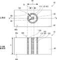
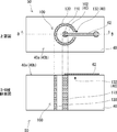
- FIG. 3 is a diagram showing a wiring board 50 according to the first embodiment.
- the upper view of FIG. 3 is a top view of the wiring board 50 as viewed from the side of the surface 40a of the silicon substrate 40 (the same applies to the drawings described later).
- the lower view of FIG. 3 is a cross-sectional view showing a cross section taken along line AA in the top view (the same applies to the drawings described later).
- the wiring board 50 has a silicon substrate 40 and a through electrode 100.
- the silicon substrate 40 is made of high resistance silicon having an electrical resistivity of 1000 ⁇ ⁇ cm or more.
- the through electrode 100 is, for example, a coaxial TSV.
- the through silicon via 100 has a central conductor 110 that penetrates the silicon substrate 40 and an outer conductor 120.
- the outer conductor 120 is formed around the central conductor 110.
- the through electrode 100 is formed by the central conductor 110 and the outer conductor 120.
- an insulating layer 102 is provided between the central conductor 110 and the outer conductor 120 by a silicon substrate 40. That is, the central conductor 110 and the outer conductor 120 are electrically insulated by the silicon substrate 40.
- the entire side surface of the outer conductor 120 penetrates the silicon substrate 40.
- the central conductor 110 is formed in a cylindrical shape (columnar shape), for example.
- the outer conductor 120 is formed in, for example, a cylindrical shape (cylindrical shape).
- the outer conductor 120 according to the first embodiment is formed so as to have a continuous annular shape (annular shape) in a cross section on an arbitrary surface parallel to the surface 40a of the silicon substrate 40.
- the outer conductor 120 according to the first embodiment is formed so as to surround the central conductor 110 so as to form a continuous annular shape.
- the outer conductor 120 according to the first embodiment is formed so as to form a continuous annular shape when viewed from the front surface 40a (or the back surface 40b). Further, in other words, the outer conductor 120 according to the first embodiment is formed around the central conductor 110 so as to form a continuous annular shape orbiting the central conductor 110. Therefore, the outer conductor 120 according to the first embodiment has the same cross-sectional shape (that is, the cutting position) on an arbitrary surface parallel to the surface 40a of the silicon substrate 40, regardless of the position in the thickness direction (that is, the cutting position) of the silicon substrate 40 (annular). ) Is formed. That is, the outer conductor 120 according to the first embodiment is formed so as to have a continuous shape in the thickness direction of the silicon substrate 40.
- the central conductor 110 and the outer conductor 120 may have the following configurations. That is, the central conductor 110 has the shape of a first cylinder.
- the outer conductor 120 has a second cylinder having the same central axis as the central axis of the first cylinder and having a diameter larger than the diameter D1 of the first cylinder, and the same center as the central axis of the first cylinder. It is formed in a region surrounded by a third cylinder having a shaft and a diameter D2 larger than the diameter of the second cylinder.
- the width W2 of the outer conductor 120 is preferably narrow. Specifically, the width W2 of the outer conductor 120 is preferably 0.5 times or less the diameter D1 (external dimensions) of the center conductor 110. In other words, the difference between the diameter of the third cylinder and the diameter of the second cylinder is 0.5 times or less the diameter of the first cylinder.
- the central conductor 110 plays the role of a core wire through which high-frequency control signals and read signals are transmitted
- the outer conductor 120 plays the role of ground. Therefore, when an electric system having a characteristic impedance of, for example, 50 ⁇ is connected to both ends of the through electrode 100, and a high frequency signal of 1 GHz or more is transmitted from one terminal of the through electrode 100 to the other terminal, the reflection is reduced.
- Design the layer width W1. Specifically, the through electrode 100 is designed so that S11 (reflection coefficient or reflection characteristic of the input terminal) is -10 dB or less.
- the thickness H of the silicon substrate 40 is about 300 ⁇ m. Further, the diameter D1 of the central conductor 110 is preferably 50 ⁇ m or less.
- the central conductor 110 and the outer conductor 120 are metals (conductors), and are normal conductive metals having a relatively low electrical resistivity such as copper (Cu) or superconducting materials such as niobium (Nb) and aluminum (Al). Metal is preferred.
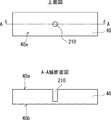
- FIGS. 4 to 11 are diagrams showing a method of manufacturing the wiring board 50 according to the first embodiment.
- the upper view shows a top view
- the lower view shows a cross-sectional view.
- the top view is a view seen from the side of the front surface 40a of the silicon substrate 40 or the side of the back surface 40b when the silicon substrate 40 is turned inside out.
- a silicon substrate 40 is prepared.
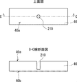
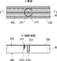
- a non-through hole 210 (blind via) for the central conductor 110 is formed on the surface 40a of the silicon substrate 40 by surface processing such as etching. That is, the surface 40a (first surface) of the silicon substrate 40 is surface-processed to form the non-through hole 210 for the central conductor 110.
- the non-through hole 210 is a hole that does not penetrate the silicon substrate 40.
- a conductor seed layer 200 is formed on the entire surface 40a of the silicon substrate 40 by, for example, sputtering or thin film deposition.
- the conductor forming the seed layer 200 is, for example, copper (Cu), but the conductor is not limited to this.
- the diameter (external dimension) D1 of the central conductor 110 is relatively large, the aspect ratio (hole depth / hole diameter) of the non-through hole 210 is small. Therefore, since the spatter can reach the bottom 210b of the non-through hole 210, the seed layer 200 can also be formed on the bottom 210b.
- the seed layer 200 is connected to the electrode, and a conductor film 201 such as a Cu film is formed by plating to fill the non-through hole 210 with a conductor.
- a conductor film 201 such as a Cu film is formed by plating to fill the non-through hole 210 with a conductor.
- the central conductor 110 is formed.
- the seed layer 200 is also formed on the bottom 210b of the non-through hole 210, it is possible to form the central conductor 110 up to the bottom 210b of the non-through hole 210 by plating.
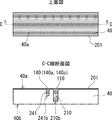
- the conductor film 201 is subjected to surface processing such as etching to obtain a pad 202 (center electrode; electrodes 42, 44) for the center conductor 110 and a ground plane 204 (center electrode; electrodes 42, 44). Solid pattern) and.
- the pad 202 and the ground plane 204 are electrically insulated by etching or the like. In this way, the pad 202 of the central conductor 110 and the ground plane 204 can be easily formed.
- the silicon substrate 40 is turned inside out, and the back surface 40b (second surface) of the silicon substrate 40 is subjected to surface processing such as etching, so that the outer conductor 120 is formed around the central conductor 110.
- a hole 220 (via) for an outer conductor is formed. That is, the outer conductor hole 220 is formed around the central conductor 110 by surface-processing the second surface, which is the surface opposite to the first surface of the silicon substrate 40.
- the outer conductor hole 220 is formed until it reaches the ground plane 204 formed on the surface 40a.
- the ground plane 204 formed on the front surface 40a of the silicon substrate 40 is connected to the electrode, and a conductor film 230 such as a Cu film is formed on the back surface 40b of the silicon substrate 40 by plating.
- the outer conductor hole 220 is filled with a conductor such as Cu.
- the outer conductor 120 is formed.
- the outer conductor hole 220 is formed until it reaches the ground plane 204, it is possible to form the outer conductor 120 by plating. Further, since the outer conductor hole 220 is formed until it reaches the ground plane 204, the outer conductor 120 is electrically connected to the ground plane 204.
- the back surface 40b of the silicon substrate 40 is thinned.
- the thinning treatment may be performed by, for example, polishing or grinding.
- the extra conductor film 230 formed on the back surface 40b is removed, and the central conductor 110 is exposed on the back surface 40b. That is, the back surface 40b (second surface) is surface-processed so that the central conductor 110 is exposed on the back surface 40b (second surface).
- the through electrode 100 which is a coaxial TSV, is formed on the silicon substrate 40.
- a ground plane having a solid pattern similar to the ground plane 204 and a pad (center electrode) similar to the pad 202 may be formed on the back surface 40b of the silicon substrate 40.
- the through electrode 100 is formed by a central conductor 110 penetrating the silicon substrate 40 and an outer conductor 120 formed around the central conductor 110.
- the central conductor 110 and the outer conductor 120 are electrically insulated by a silicon substrate 40 formed of high-resistance silicon. Therefore, the dielectric loss in the through electrode 100 can be suppressed. Therefore, the coherence time of the quantum calculation in the superconducting circuit device 1 can be maintained for a long time.
- the outer conductor 120 is formed in a tubular shape (not limited to a cylinder) surrounding the central conductor 110.
- the outer conductor 120 according to the first embodiment has a continuous annular shape (not limited to a circle) in a cross section of the silicon substrate 40 on an arbitrary surface parallel to the surface 40a (first surface) of the silicon substrate 40. It is formed so as to be.
- the outer conductor hole 220 is formed in the back surface 40b. To form. Then, the outer conductor 120 is formed by filling the outer conductor hole 220 with the conductor by plating. Specifically, when the center conductor 110 is formed from the surface 40a of the silicon substrate 40, the ground plane 204 is formed on the surface 40a by plating. Then, the outer conductor hole 220 is formed from the back surface 40b until it reaches the ground plane 204 formed on the front surface 40a. Then, when plating the back surface 40b, the ground plane 204 formed on the front surface 40a is connected to the electrodes.
- the outer conductor 120 having a narrow width can be formed by plating. That is, the outer conductor 120 can be formed so that the width (W2) of the outer conductor 120 is 0.5 times or less the external dimension (D1) of the central conductor 110. Therefore, it is possible to form a through electrode 100 having a small outer diameter D2 (external dimension). That is, by forming the holes 220 for the outer conductor having a large aspect ratio and connecting the ground plane 204 formed on the surface 40a instead of the seed layer to the electrodes, the outer conductor 120 having a large aspect ratio can be easily formed. Can be formed.
- the ground plane 204 provided at the bottom of the outer conductor hole 220 is connected to the electrode, even if the aspect ratio of the outer conductor hole 220 is large, the conductor is surely filled in the outer conductor hole 220 without any gap. Will be done.
- the ground plane 204 formed on the front surface 40a is connected to the electrode, so that it is not necessary to form the seed layer by sputtering when the outer conductor 120 is formed.
- a hole having a large aspect ratio is formed in order to form the outer conductor 120 having a large aspect ratio, and a seed layer is formed in the hole by sputtering.
- the spatter may not reach the deep part (bottom, etc.) of the hole because it is blocked by the side wall of the shallow part of the hole. Therefore, it may not be possible to form a seed layer in a deep portion of a hole having a large aspect ratio.
- the outer conductor 120 even if an attempt is made to form the outer conductor 120 by plating, since the seed layer is formed only in the shallow part of the hole, the conductor can be formed only in the shallow part of the hole, and the conductor cannot be filled in the entire hole. There is a risk.
- the outer conductor 120 when the outer conductor 120 is formed, it is not necessary to form the seed layer by sputtering, so that the outer conductor 120 having a large aspect ratio is formed more reliably. Can be done.
- the surface 40a (first surface) of the silicon substrate 40 is surface-processed to form a non-through hole 210 for the central conductor 110 (FIG. 5). Then, by plating the surface 40a, the non-through hole 210 is filled with a conductor to form the central conductor 110, and the ground plane is formed on the surface 40a (FIGS. 6 to 8).
- the ground plane 204 By forming the ground plane 204 in this way, the ground plane 204 can be easily formed. That is, in the process of forming the central conductor 110, the ground plane 204 can also be formed.
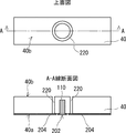
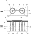
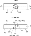
- FIG. 12 is a diagram showing a wiring board 50 according to the second embodiment.
- the top view (upper view) is a view of the wiring board 50 viewed from the side of the surface 40a of the silicon substrate 40.
- the bottom view (lower figure) is a view of the wiring board 50 viewed from the back surface 40b side of the silicon substrate 40.
- the cross-sectional view (middle view) shows a cross-sectional view taken along line BB in the top view and the bottom view (the same applies to the views described later).
- the wiring board 50 according to the second embodiment has a silicon substrate 40 formed of high resistance silicon and a through electrode 100 which is, for example, a coaxial TSV.
- the through silicon via 100 has a central conductor 110 that penetrates the silicon substrate 40 and an outer conductor 130.
- the outer conductor 130 corresponds to the outer conductor 120 according to the first embodiment. Similar to the outer conductor 120 according to the first embodiment, the outer conductor 130 is formed around the central conductor 110.
- An insulating layer 102 is provided between the central conductor 110 and the outer conductor 130 by a silicon substrate 40. That is, the central conductor 110 and the outer conductor 130 are electrically insulated by the silicon substrate 40.
- the central conductor 110 is formed in a columnar shape such as a cylindrical shape.
- the outer conductor 130 according to the second embodiment is formed so as to have an annular shape (annular shape) in which a part is cut out in a cross section on an arbitrary surface parallel to the surface 40a of the silicon substrate 40.
- the outer conductor 130 according to the second embodiment is formed so as to have a shape in which a part of an annulus (annular) is missing in a cross section on an arbitrary surface parallel to the surface 40a of the silicon substrate 40. ..
- the outer conductor 130 according to the second embodiment is not a continuous annular shape in a cross section on an arbitrary surface parallel to the surface 40a of the silicon substrate 40.
- the outer conductor 130 according to the second embodiment is formed so as to have a C-shape in a cross section on an arbitrary surface parallel to the surface 40a of the silicon substrate 40. That is, the outer conductor 130 according to the second embodiment is formed so as to have a C shape when viewed from the surface 40a of the silicon substrate 40.
- the outer conductor 130 according to the second embodiment is formed so as to surround the central conductor 110 so as to form an annular shape partially cut out.
- the outer conductor 130 according to the second embodiment is formed so as to form an annular shape in which a part of the outer conductor 130 is cut out when viewed from the front surface 40a (or the back surface 40b). Further, in other words, the outer conductor 130 according to the second embodiment is formed so as to form an annular shape in which a part of the outer conductor 130 orbiting the central conductor 110 is cut out around the central conductor 110.
- the outer conductor 130 according to the second embodiment has a notch 132 on the side surface.
- the notch 132 is formed of a silicon substrate 40.
- the outer conductor 130 according to the second embodiment is formed in a cylindrical shape (cylindrical shape) having a groove (notch 132) formed on the side surface. Therefore, the outer conductor 130 according to the second embodiment has the same cross-sectional shape on an arbitrary surface parallel to the surface 40a of the silicon substrate 40, regardless of the position in the thickness direction (that is, the cutting position) of the silicon substrate 40 (C). It is formed so as to have a character shape).
- the outer conductor 120 according to the first embodiment is formed so as to have a continuous shape (C-shape) in the thickness direction of the silicon substrate 40.
- the reason why the outer conductor 130 according to the second embodiment is formed so that its cross section has a C-shape as described above will be described later.
- the outer conductor 120 has a cross-sectional shape on an arbitrary surface parallel to the surface 40a of the silicon substrate 40, which is the thickness of the silicon substrate 40. It is formed so as to be the same regardless of the position in the longitudinal direction. Therefore, the wiring board 50 (through silicon via 100) according to the second embodiment can be manufactured by substantially the same method as the manufacturing method according to the first embodiment.
- 13 to 16 are diagrams for explaining the effect of forming the outer conductor 130 according to the second embodiment into the shape shown in FIG.
- the bond (adhesion) between the conductor formed by plating (center conductor 110) and the silicon substrate 40 is weak. Therefore, when pressure is applied to the center conductor 110, the center conductor 110 may be peeled off from the silicon substrate 40.
- FIG. 13 is a diagram for explaining a problem in the case of flip-chip connecting the quantum circuit chip 20 to the silicon substrate 40 on which the through electrode 100 according to the first embodiment is formed.
- FIG. 14 and 15 are diagrams for explaining an example of a method for reducing the problems described with reference to FIG.
- the leader wire 62 is connected to the center conductor 110.
- An insulating layer 64 is provided on the front surface 40a (or the back surface 40b) of the silicon substrate 40 in order to electrically insulate the leader wire 62 and the outer conductor 120.
- the position of the bump 10 can be shifted from directly above the central conductor 110. Therefore, when the bump 10 is pressed in the direction indicated by the arrow A at the time of flip-chip connection, the pressure applied to the center conductor 110 can be suppressed, and the center conductor 110 can be suppressed from peeling from the silicon substrate 40. Further, the leader wire 62 electrically connects the quantum circuit 22 and the center conductor 110.
- the insulating layer 64 it is necessary to form an insulating layer 64 on the surface 40a in order to electrically insulate the leader wire 62 and the outer conductor 120. Then, SiO 2 or the like can be considered as the material of the insulating layer 64. However, as described above, since the insulating material such as SiO 2 has a large dielectric loss, there is a problem that the coherence time of the quantum circuit 22 may be shortened.
- FIG. 16 is a diagram showing a state in which the leader wire 62 is connected to the through electrode 100 according to the second embodiment.
- the leader wire 62 is connected to the center conductor 110.
- the leader line 62 is arranged in the notch 132 on the front surface 40a or the back surface 40b.
- the leader wire 62 and the outer conductor 130 can be electrically insulated without forming an insulating layer on the front surface 40a or the back surface 40b. Therefore, it is possible to suppress the damage of the through electrode 100 while suppressing the shortening of the coherence time of the quantum circuit 22. That is, by using the through electrode 100 according to the second embodiment, it is possible to increase the mechanical strength of the through electrode 100 while suppressing the shortening of the coherence time of the quantum circuit 22.
- FIG. 17 to 19 are diagrams for explaining a mounting example of the through silicon via 100 according to the second embodiment.
- the wiring board 50, the reading unit 3 and the control unit 4 are connected via a socket 70.
- the socket 70 is configured by mounting a large number of probe pins 74 made of metal on a housing 72 made of ceramic. By crimping these probe pins 74 to the through electrode 100, the probe pin 74 and the through electrode 100 are electrically connected.
- the through silicon via 100 may be damaged such as peeling (falling off) as described above.
- the coefficient of linear expansion of Cu is larger than the coefficient of linear expansion of Si, when cooled from room temperature to an extremely low temperature of about 10 mK, Cu shrinks more strongly than Si.
- the temperature difference between the room temperature and the extremely low temperature is about 300 degrees, the impact of this shrinkage difference is large.
- the degree of adhesion between the Cu (conductor) of the through electrode 100 and the Si (silicon substrate 40) is further reduced, so that the possibility of damage to the through electrode 100 is increased. This is a problem peculiar to superconducting quantum computers that cool to extremely low temperatures.
- FIG. 18 and 19 are diagrams showing a mounting example in which two through electrodes 100 are connected by wiring.
- 18 and 19 show inductors (wiring) for controlling the quantum circuit 22.
- Various wirings are connected to the central conductor 110 (core wire) of the through electrode 100.
- FIG. 18 is a diagram showing a state in which the central conductors 110 of the two through electrodes 100 according to the first embodiment are connected by wiring 66.
- the wiring 66 and the outer conductor 120 it is necessary to form an insulating layer 64 on the silicon substrate 40.
- the insulating material has a large dielectric loss, there is a problem that the coherence time of the quantum circuit 22 may be shortened.
- FIG. 19 is a diagram showing a state in which the central conductors 110 of the two through electrodes 100 according to the second embodiment are connected by wiring 66.
- the wiring 66 is arranged in the notch 132.
- the wiring 66 and the outer conductor 130 can be electrically insulated without forming an insulating layer on the silicon substrate 40. Therefore, it is possible to suppress shortening the coherence time of the quantum circuit 22. That is, by using the through silicon via 100 according to the second embodiment, wiring of various layouts can be performed while suppressing shortening of the coherence time of the quantum circuit 22.
- the length L1 (FIG. 12) of the notch 132 should not be too long from the viewpoint of high frequency characteristics. This is because if the length L1 (separation distance) of the notch 132 is too long, it becomes difficult to suppress the leakage of the electromagnetic field and the crosstalk associated therewith. On the other hand, if the length L1 of the notch 132 is too short, it becomes difficult to connect the leader wire 62 and the wiring 66 to the center conductor 110 so as to insulate the outer conductor 130. Therefore, it is preferable that the length L1 of the cutout portion 132 is longer than the width of the leader wire 62 and the wiring 66 and is equal to or less than the diameter D1 of the central conductor 110.
- the separation distance L1 of the notched portion of the outer conductor 130 is equal to or less than the diameter of the center conductor 110.
- L1 is preferably 2 ⁇ m or more and 50 ⁇ m or less in consideration of suppressing the impedance to about 50 ⁇ .
- the third embodiment is different from the first and second embodiments in that the shape of the outer conductor is different from that of the first and second embodiments.
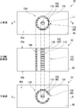
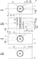
- FIG. 20 is a diagram showing a wiring board 50 according to the third embodiment.
- the top view (top view) is a view of the wiring board 50 viewed from the side of the surface 40a of the silicon substrate 40.
- the bottom view (second view from the bottom) is a view of the wiring board 50 viewed from the back surface 40b side of the silicon substrate 40.
- the cross-sectional view (second view from the top) shows a cross section taken along line CC in the top view and the bottom view (the same applies to the views described later).
- the cross-sectional view (bottom view) shows the DD line cross section in the CC line cross section (second view from the top).
- the wiring board 50 according to the third embodiment has a silicon substrate 40 formed of high resistance silicon and a through electrode 100 which is, for example, a coaxial TSV.
- the through silicon via 100 has a central conductor 110 that penetrates the silicon substrate 40 and an outer conductor 140.
- the outer conductor 140 corresponds to the outer conductor 120 according to the first embodiment. Similar to the outer conductor 120 according to the first embodiment, the outer conductor 140 is formed around the central conductor 110.
- An insulating layer 102 is provided between the central conductor 110 and the outer conductor 140 by a silicon substrate 40. That is, the central conductor 110 and the outer conductor 140 are electrically insulated by the silicon substrate 40.
- the central conductor 110 is formed in a columnar shape such as a cylindrical shape.
- the outer conductor 140 according to the third embodiment is formed on the side of the outer conductor portion 140a (first outer conductor portion) formed on the side of the front surface 40a of the silicon substrate 40 and the side of the back surface 40b of the silicon substrate 40. It has an outer conductor portion 140b (second outer conductor portion). Therefore, the outer conductor portion 140a does not penetrate the silicon substrate 40. Similarly, the outer conductor portion 140b does not penetrate the silicon substrate 40.
- the outer conductor 140 may have an outer conductor portion 140c (third outer conductor portion) between the outer conductor portion 140a and the outer conductor portion 140b.
- the outer conductor portion 140a and the outer conductor portion 140b are electrically connected via the outer conductor portion 140c.
- the outer conductor portion 140c is formed in a cylindrical shape (cylindrical shape) having no groove on the side surface, similarly to the outer conductor 120 according to the first embodiment. That is, the outer conductor portion 140c is formed so as to form a continuous annular shape in the cross section of the silicon substrate 40 on an arbitrary surface parallel to the surface 40a of the silicon substrate 40.
- the outer conductor portion 140c is formed so as to surround the central conductor 110 so as to form a continuous ring.
- the outer conductor portion 140c is formed so as to form a continuous annular shape when viewed from the front surface 40a (or the back surface 40b).
- the outer conductor portion 140c is formed around the central conductor 110 so as to form a continuous annular shape orbiting the central conductor 110.
- the outer conductor 140 does not have to have the outer conductor portion 140c between the outer conductor portion 140a and the outer conductor portion 140b.
- the outer conductor portion 140a and the outer conductor portion 140b may be electrically connected by being physically directly connected. That is, the outer conductor portion 140a and the outer conductor portion 140b are electrically connected regardless of the presence or absence of the outer conductor portion 140c. Therefore, similarly to the above-described embodiment, in the outer conductor 140, electrical conduction is ensured between the front surface 40a side and the back surface 40b side of the silicon substrate 40.
- the outer conductor portion 140a according to the third embodiment is a circular ring in which a part is cut out in a cross section on a surface parallel to the surface 40a of the silicon substrate 40. It is formed so as to have a shape (annular shape). Therefore, the outer conductor portion 140a according to the third embodiment has a notch portion 142A (first notch portion) on the side surface. In other words, the outer conductor portion 140a according to the third embodiment is formed so as to have a C-shape in a cross section on an arbitrary surface parallel to the surface 40a of the silicon substrate 40.
- the outer conductor portion 140a according to the third embodiment is formed so as to have a C shape when viewed from the surface 40a of the silicon substrate 40.
- the outer conductor portion 140b according to the third embodiment is formed so as to have an annular shape (annular shape) in which a part is cut out in a cross section on a surface parallel to the back surface 40b of the silicon substrate 40.
- the outer conductor portion 140b according to the third embodiment has a notch portion 142B (second notch portion) on the side surface.
- the outer conductor portion 140b according to the third embodiment is formed so as to have a C-shape in a cross section on an arbitrary surface parallel to the back surface 40b of the silicon substrate 40.
- the outer conductor portion 140b according to the third embodiment is formed so as to have a C shape when viewed from the back surface 40b of the silicon substrate 40.
- the notches 142A and 142B are formed of a silicon substrate 40.
- the outer conductor portions 140a and 140b according to the third embodiment are formed in a cylindrical shape (cylindrical shape) having grooves formed on the side surfaces.
- the outer conductor 140 is formed in a tubular shape having a groove (notch portion) formed on the side surface on the side of the front surface 40a and the side of the back surface 40b of the silicon substrate 40.
- the outer conductor portions 140a and 140b according to the third embodiment are formed so as to surround the central conductor 110 so as to form a continuous annular shape. Further, in other words, the outer conductor portions 140a and 140b according to the third embodiment are formed so as to form a continuous annular shape when viewed from the front surface 40a (or the back surface 40b). Further, in other words, the outer conductor portions 140a and 140b according to the third embodiment are formed around the central conductor 110 so as to form a continuous annular shape orbiting the central conductor 110.
- the position (first position) of the notch portion 142A in the outer conductor portion 140a does not have to correspond to the position (second position) of the notch portion 142B in the outer conductor portion 140b.
- the notch 142A in the outer conductor portion 140a is provided on the right side of the central conductor 110
- the notch 142B in the outer conductor portion 140b is provided on the left side of the center conductor 110.
- the position (first position) of the notch 142A in the outer conductor portion 140a formed on the side of the front surface 40a is the position of the outer conductor portion formed on the side of the back surface 40b.
- the orientation of the position of the notch 142A on the front surface 40a with respect to the center conductor 110 is different from the orientation of the position of the notch 142B on the back surface 40b with respect to the center conductor 110. That is, the first position with respect to the central conductor 110 is different from the second position with respect to the central conductor 110.
- the outer conductor 140 according to the third embodiment is formed as described above.
- the positions of the notches 132 correspond to each other on the front surface 40a and the back surface 40b of the silicon substrate 40.
- the orientation of the position of the notch 132 on the front surface 40a with respect to the center conductor 110 is the same as the orientation of the position of the notch 132 on the back surface 40b with respect to the center conductor 110. Therefore, in the structure according to the second embodiment, there is a restriction that the direction of the wiring drawn out from the central conductor 110 must be the same on the front surface 40a and the back surface 40b of the silicon substrate 40.
- the orientation of the position of the notch 142A on the front surface 40a with respect to the center conductor 110 is different from the orientation of the position of the notch 142B on the back surface 40b with respect to the center conductor 110. Therefore, by adopting the structure according to the third embodiment, the direction of the wiring drawn out from the central conductor 110 can be arbitrarily changed as described later. Therefore, the degree of freedom in wiring design is improved.
- the length L1 of the notch 142A and the length of the notch 142B from the viewpoint of suppressing the leakage of the electromagnetic field and the crosstalk associated therewith in the transmission of the high frequency signal.
- L2 should not be too long. That is, it is preferable that the length L1 of the notch portion 142A and the length L2 of the notch portion 142B are longer than the width of the wiring and are equal to or less than the diameter D1 of the central conductor 110.
- L1 and L2 are preferably 2 ⁇ m or more and 50 ⁇ m or less in consideration of suppressing the impedance to about 50 ⁇ .
- FIGS. 21 to 30 are diagrams showing a method of manufacturing the wiring board 50 according to the third embodiment.
- the upper view shows a top view
- the lower view shows a cross-sectional view.
- the top view is a view seen from the side of the front surface 40a of the silicon substrate 40 or the side of the back surface 40b when the silicon substrate 40 is turned inside out.
- a silicon substrate 40 is prepared.
- a non-through hole 210 (blind via) for the central conductor 110 is formed on the surface 40a of the silicon substrate 40 by surface processing such as etching. That is, the surface 40a (first surface) of the silicon substrate 40 is surface-processed to form the non-through hole 210 for the central conductor 110.
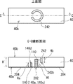
- the outer conductor hole 241 for the outer conductor 140 (outer conductor portion 140a) is formed around the central conductor 110.
- First hole for outer conductor is formed.
- the outer conductor hole 241 is formed so that the shape on the surface parallel to the surface 40a of the silicon substrate 40 is C-shaped. That is, the outer conductor hole 241 is formed so as to have a C shape when viewed from the surface 40a of the silicon substrate 40.
- the surface is processed so that the depth of the outer conductor hole 241 is shallower than the depth of the non-through hole 210 for the central conductor 110. That is, the outer conductor hole 241 is a non-through hole (blind via).
- a seed layer 200 (first seed layer) of a conductor (Cu or the like) is formed on the entire surface 40a of the silicon substrate 40 by, for example, sputtering.
- the aspect ratio (hole depth / hole diameter) of the non-through hole 210 is small, the spatter can reach the bottom 210b of the non-through hole 210. Therefore, the seed layer 200 can also be formed on the bottom 210b.
- the width of the outer conductor hole 241 is narrower than the diameter of the non-through hole 210, but the depth of the outer conductor hole 241 is shallower than the depth of the non-through hole 210. It is small enough that spatter can reach the bottom 241b of the outer conductor hole 241. Therefore, the seed layer 200 can also be formed on the bottom 241b.
- the seed layer 200 is connected to the electrode, and the seed layer 200 is plated.
- a conductor film 201 such as a Cu film by plating
- the non-through hole 210 and the outer conductor hole 241 are filled with a conductor.
- a part of the central conductor 110 and the outer conductor 140 (outer conductor portions 140a, 140c) is formed.
- the seed layer 200 is also formed on the bottom 210b of the non-through hole 210, it is possible to form the central conductor 110 by plating.
- the seed layer 200 is also formed on the bottom portion 241b of the outer conductor hole 241, it is possible to form the outer conductor portion 140a (and the outer conductor portion 140c) by plating.
- the conductor film 201 is subjected to surface processing such as etching to obtain a pad 202 (center electrode; electrodes 42, 44) for the center conductor 110 and a ground plane 204 (center electrode; electrodes 42, 44). Solid pattern) and.
- the pad 202 and the ground plane 204 are electrically insulated by etching or the like.
- the outer conductor portion 140a is electrically connected to the ground plane 204.
- a hole for the outer conductor which is a hole for the outer conductor 140 (outer conductor portion 140b), is formed around the central conductor 110.
- 242 hole for the second outer conductor is formed. That is, the outer conductor hole 242 is formed around the central conductor 110 by processing the second surface, which is the surface opposite to the first surface of the silicon substrate 40.
- the outer conductor hole 242 is formed so that the shape on the surface parallel to the back surface 40b of the silicon substrate 40 is C-shaped. That is, the outer conductor hole 242 is formed so as to have a C shape when viewed from the back surface 40b of the silicon substrate 40. Further, the surface is processed so that the depth of the outer conductor hole 242 is shallower than the depth of the non-through hole 210 for the central conductor 110. That is, the outer conductor hole 242 is a non-through hole (blind via). Further, surface processing is performed so that the bottom portion 242b of the outer conductor hole 242 becomes deep enough to reach at least the bottom portion 140d of the outer conductor 140 (outer conductor portions 140a, 140c) formed in the step of FIG. 26.
- the thickness of the silicon substrate 40 is H'. Further, the height (depth) of the central conductor 110 is H1, the height of the outer conductors 140 (outer conductor portions 140a, 140c) formed in the process of FIG. 26 is Ha, and the depth of the outer conductor holes 242 is set. Let Hb. At this time, the following equation 1 holds. (H'-Ha) ⁇ Hb ⁇ H1 ... (1) That is, the total of the depth Ha of the outer conductor hole 241 (first outer conductor hole) and the depth Hb of the outer conductor hole 242 (second outer conductor hole) is the thickness of the silicon substrate 40. It is H'or higher.
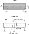
- a seed layer 250 (second seed layer) of a conductor (Cu or the like) is formed on the entire back surface 40b of the silicon substrate 40 by, for example, sputtering.
- the width of the outer conductor hole 242 is narrower than the diameter of the non-through hole 210
- the depth of the outer conductor hole 242 is shallower than the depth of the non-through hole 210, so that the aspect ratio of the outer conductor hole 242 is It is small enough that spatter can reach the bottom 242b of the outer conductor hole 242. Therefore, the seed layer 250 can also be formed on the bottom 242b.
- the seed layer 250 is connected to the electrode, and the seed layer 250 is plated.
- a conductor film 251 such as a Cu film by plating
- the conductor is filled in the outer conductor hole 242.
- a part of the outer conductor 140 (outer conductor portions 140b, 140c) is formed.
- the seed layer 250 is also formed on the bottom portion 242b of the outer conductor hole 242, it is possible to form the outer conductor portion 140b (and the outer conductor portion 140c) by plating.
- the back surface 40b of the silicon substrate 40 is thinned in the same manner as in the process of FIG.
- the thinning treatment may be performed by, for example, polishing or grinding.
- the extra conductor film 251 formed on the back surface 40b is removed, and the central conductor 110 and the outer conductor portion 140b are exposed on the back surface 40b.
- the back surface 40b (second surface) is surface-processed so that the central conductor 110 and the outer conductor portion 140b are exposed on the back surface 40b (second surface).
- the through electrode 100 which is a coaxial TSV, is formed on the silicon substrate 40.
- a ground plane having a solid pattern similar to the ground plane 204 and a pad (center electrode) similar to the pad 202 may be formed on the back surface 40b of the silicon substrate 40.
- the outer conductor portion 140c formed in a continuous ring shape exists. Then, it is preferable to increase the height of the outer conductor portion 140c (the length of the silicon substrate 40 in the thickness direction).
- the depth of the outer conductor holes 241,242 it is necessary to increase the depth of the outer conductor holes 241,242. However, if the depth of the outer conductor holes 241,242 is increased, there is a high possibility that the sputtering does not reach the bottom of the outer conductor holes 241,242 during sputtering. Therefore, the depth of the outer conductor holes 241,242 is preferably made deeper as long as the spatter reaches the bottom.
- the position of the notch portion 142A on the side of the front surface 40a and the position of the notch portion 142B on the side of the back surface 40b are related to the central conductor 110.
- the positional relationship is 180 degrees off.
- the positional relationship between the two is not limited to such a thing.
- the position of the notch 142A on the side of the front surface 40a and the position of the notch 142B on the side of the back surface 40b may be displaced by 90 degrees with respect to the central conductor 110.
- the position of the notch 142B on the back surface 40b side may be the upper side (or lower side) of the central conductor 110 in FIG. 20.
- the directions of the notches 142A and 142B with respect to the central conductor 110 can be set to any direction on the front surface 40a and the back surface 40b.
- the through silicon via 100 according to the third embodiment described above is configured such that the outer conductor 140 is provided with notches 142A and 142B. Therefore, the wiring board 50 according to the third embodiment can exert substantially the same effect as the wiring board 50 according to the second embodiment.
- the orientation of the position of the notch 142A on the front surface 40a with respect to the center conductor 110 is different from the orientation of the position of the notch 142B on the back surface 40b with respect to the center conductor 110. ing. Therefore, the wiring board 50 according to the third embodiment can arbitrarily change the direction of the wiring drawn from the central conductor 110 of the through electrode 100. Therefore, the degree of freedom in wiring design is improved.
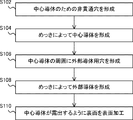
- FIG. 31 is a flowchart showing a method of manufacturing the wiring board 50 according to the present embodiment.
- a non-through hole for the central conductor is formed by surface-processing the surface 40a (first surface) of the silicon substrate 40 made of silicon having an electrical resistivity of 1000 ⁇ ⁇ cm or more (step S102). ). This step corresponds to FIGS. 5 and 22.
- a central conductor is formed by filling the non-through holes with a conductor by plating (step S104). This step corresponds to FIGS. 6 to 7 and 24 to 25.
- step S106 By processing at least the back surface 40b (second surface) of the silicon substrate 40, at least one hole for an outer conductor is formed around the central conductor (step S106). This step corresponds to FIGS. 9, 23 and 27.
- the outer conductor is formed by filling the holes for the outer conductor with the conductor by plating (step S108). This step corresponds to FIGS. 10, 24-25 and 28-29.
- the back surface 40b is surface-processed so that the central conductor is exposed on the back surface 40b of the silicon substrate 40 (step S110). This step corresponds to FIGS. 11 and 30.
- a central conductor can be formed on the silicon substrate 40, and an outer conductor can be formed around the central conductor at a distance from the central conductor. Therefore, it is possible to easily manufacture a wiring board 50 in which a through electrode 100 electrically insulated by a silicon substrate 40 formed of high resistance silicon between a central conductor and an outer conductor is formed on the silicon substrate 40. it can. Further, since the outer conductor having a high aspect ratio can be formed by this method, the through electrodes 100 can be integrated at high density on the silicon substrate 40.
- each step of the flowchart described above may be omitted. Further, the order of each step in the above-mentioned flowchart can be changed as appropriate. Moreover, each step described above may be executed at the same time as another step. For example, in the flowchart shown in FIG. 31, the processes S106 to S108 may be performed at the same time as the processes S102 to S104. Alternatively, the process of S106 may be executed before the process of S104.
- the front surface 40a and the back surface 40b may be reversed. That is, in the above-described embodiment, in the method for manufacturing the wiring board 50, a non-through hole is formed in the front surface 40a (first surface) of the silicon substrate 40 to form a central conductor, and the back surface 40b of the silicon substrate 40 ( It is assumed that a hole for an outer conductor is formed on the second surface) to form an outer conductor. However, a non-through hole is formed on the back surface 40b (first surface) of the silicon substrate 40 to form a central conductor, and a hole for an outer conductor is formed on the front surface 40a (second surface) of the silicon substrate 40 to form an external conductor. A conductor may be formed.
- a non-through hole and a hole for an outer conductor are formed by etching, but the method of forming these holes is not limited to etching.
- the seed layer is formed by sputtering, but the method of forming the seed layer is not limited to sputtering.
- (Appendix 1) A silicon substrate made of silicon with an electrical resistivity of 1000 ⁇ ⁇ cm or more, and It has a through electrode formed on the silicon substrate and has The through electrode is formed by a central conductor penetrating the silicon substrate and an outer conductor formed around the central conductor. The central conductor and the outer conductor are electrically insulated by the silicon substrate. Wiring board. (Appendix 2) The width of the outer conductor is 0.5 times or less the external dimension of the center conductor. The wiring board according to Appendix 1. (Appendix 3) The outer conductor is formed so as to surround the central conductor so as to form a continuous ring. The wiring board according to Appendix 1 or 2.
- the outer conductor is formed so as to surround the central conductor so as to form an annular shape partially cut out.
- the wiring board according to Appendix 1 or 2. (Appendix 5)
- the distance between the notched portions of the outer conductor is equal to or less than the diameter of the center conductor.
- the wiring board according to Appendix 4. (Appendix 6)
- the outer conductor is formed so as to have a continuous shape in the thickness direction of the silicon substrate.
- the outer conductor is formed on a first outer conductor portion formed on the side of the first surface of the silicon substrate and a second surface of the silicon substrate opposite to the first surface.
- the wiring board according to Appendix 1 or 2. (Appendix 8)
- the outer conductor is a third outer conductor portion formed between the first outer conductor portion and the second outer conductor portion so as to surround the central conductor in a continuous annular shape. 7.
- a non-through hole for the central conductor of the through electrode is formed.
- the central conductor is formed.
- At least one hole for the outer conductor of the through electrode around the central conductor by at least surface processing the second surface of the silicon substrate, which is the surface opposite to the first surface.
- Form a hole for the outer conductor The outer conductor is formed by filling the hole for the outer conductor with a conductor by plating.
- the second surface is surface-processed so that the central conductor is exposed on the second surface. Manufacturing method of wiring board.
- the outer conductor By connecting the ground plane to the electrode and filling the hole for the outer conductor with the conductor by plating, the outer conductor becomes an annular shape continuous or partially cut out around the central conductor. Form to surround the The method for manufacturing a wiring board according to Appendix 11. (Appendix 13) The outer conductor hole is formed from the second surface until it reaches the ground plane formed on the first surface. By connecting the ground plane to an electrode and filling the hole for the outer conductor with a conductor by plating, the outer conductor is formed so as to have a shape continuous in the thickness direction of the silicon substrate. The method for manufacturing a wiring board according to Appendix 11 or 12.
- the hole for the outer conductor has a depth shallower than the depth of the non-through hole, and has a C-shape when viewed from the first surface.
- a first hole for an outer conductor is formed around the non-through hole.
- the non-through hole is filled with a conductor to form the central conductor, and the first outer conductor hole is filled with the conductor at the first position.
- a first outer conductor portion to be a portion of the outer conductor is formed so as to surround the central conductor so as to form an annular shape in which a part is cut out.
- a first seed layer is formed on the first surface in a state where the non-through hole and the hole for the first outer conductor are formed on the first surface.
- the central conductor and the first outer conductor portion are formed.
- the method for manufacturing a wiring board according to Appendix 14. (Appendix 16) By applying surface processing to the second surface, it is a hole for the outer conductor, which has a shallower depth than the non-through hole, and has a C-shape when viewed from the second surface.
- a second hole for the outer conductor is formed around the central conductor.
- the hole for the second outer conductor is filled with the conductor, so that a part of the hole is cut at a second position where the position with respect to the center conductor is different from the first position.
- a second outer conductor portion which is a portion of the outer conductor, is formed so as to surround the central conductor so as to form a missing annular shape.
- the method for manufacturing a wiring board according to Appendix 15. (Appendix 17) A second seed layer is formed on the second surface in a state where the holes for the second outer conductor are formed on the second surface. By connecting the second seed layer to the electrode and plating the second seed layer, the second outer conductor portion is formed.
- the method for manufacturing a wiring board according to Appendix 16. (Appendix 18) The sum of the depth of the first outer conductor hole and the depth of the second outer conductor hole is equal to or greater than the thickness of the silicon substrate.
Landscapes
- Engineering & Computer Science (AREA)
- Microelectronics & Electronic Packaging (AREA)
- Containers, Films, And Cooling For Superconductive Devices (AREA)
- Structure Of Printed Boards (AREA)
- Internal Circuitry In Semiconductor Integrated Circuit Devices (AREA)
Priority Applications (4)
| Application Number | Priority Date | Filing Date | Title |
|---|---|---|---|
| US17/789,308 US20230034867A1 (en) | 2020-01-10 | 2020-01-10 | Wiring substrate and method of manufacturing the same |
| JP2021569704A JP7211540B2 (ja) | 2020-01-10 | 2020-01-10 | 配線基板及びその製造方法 |
| PCT/JP2020/000733 WO2021140664A1 (ja) | 2020-01-10 | 2020-01-10 | 配線基板及びその製造方法 |
| JP2023000961A JP7424520B2 (ja) | 2020-01-10 | 2023-01-06 | 配線基板及びその製造方法 |
Applications Claiming Priority (1)
| Application Number | Priority Date | Filing Date | Title |
|---|---|---|---|
| PCT/JP2020/000733 WO2021140664A1 (ja) | 2020-01-10 | 2020-01-10 | 配線基板及びその製造方法 |
Publications (1)
| Publication Number | Publication Date |
|---|---|
| WO2021140664A1 true WO2021140664A1 (ja) | 2021-07-15 |
Family
ID=76787807
Family Applications (1)
| Application Number | Title | Priority Date | Filing Date |
|---|---|---|---|
| PCT/JP2020/000733 Ceased WO2021140664A1 (ja) | 2020-01-10 | 2020-01-10 | 配線基板及びその製造方法 |
Country Status (3)
| Country | Link |
|---|---|
| US (1) | US20230034867A1 (https=) |
| JP (2) | JP7211540B2 (https=) |
| WO (1) | WO2021140664A1 (https=) |
Cited By (4)
| Publication number | Priority date | Publication date | Assignee | Title |
|---|---|---|---|---|
| CN115955906A (zh) * | 2023-01-20 | 2023-04-11 | 深圳量旋科技有限公司 | 超导量子芯片及其基底、及基底的制作方法 |
| CN116261392A (zh) * | 2023-01-17 | 2023-06-13 | 深圳量旋科技有限公司 | 超导量子芯片及其基底、及基底的制作方法 |
| US20240037438A1 (en) * | 2020-12-31 | 2024-02-01 | Origin Quantum Computing Technology Co., Ltd. | Superconducting quantum chip structure and fabrication method for superconducting quantum chip |
| TWI889233B (zh) * | 2024-03-11 | 2025-07-01 | 欣興電子股份有限公司 | 電路板裝置 |
Families Citing this family (2)
| Publication number | Priority date | Publication date | Assignee | Title |
|---|---|---|---|---|
| US20230262906A1 (en) * | 2022-02-11 | 2023-08-17 | Alibaba (China) Co., Ltd. | Substrate, chip, circuit package and fabrication process |
| US20250098549A1 (en) * | 2023-09-15 | 2025-03-20 | Imec Vzw | Fabrication of Through-Silicon Vias |
Citations (7)
| Publication number | Priority date | Publication date | Assignee | Title |
|---|---|---|---|---|
| JP2002334956A (ja) * | 2001-05-09 | 2002-11-22 | Fujitsu Ltd | 半導体装置の支持体及びその製造方法 |
| JP2006019455A (ja) * | 2004-06-30 | 2006-01-19 | Nec Electronics Corp | 半導体装置およびその製造方法 |
| US20100295066A1 (en) * | 2005-08-11 | 2010-11-25 | Christian Drabe | Semiconductor substrate and methods for the production thereof |
| CN103311141A (zh) * | 2013-07-05 | 2013-09-18 | 北京理工大学 | 一种同轴垂直互连导电体的制作方法 |
| CN106158835A (zh) * | 2016-07-08 | 2016-11-23 | 西安理工大学 | 一种基于硅通孔技术的低通滤波器 |
| CN109461699A (zh) * | 2018-10-22 | 2019-03-12 | 中国电子科技集团公司第三十八研究所 | 一种同轴tsv结构转接板及其制作方法 |
| US20190273197A1 (en) * | 2016-12-27 | 2019-09-05 | Intel Corporation | Superconducting qubit device packages |
Family Cites Families (4)
| Publication number | Priority date | Publication date | Assignee | Title |
|---|---|---|---|---|
| JP4192035B2 (ja) * | 2003-05-27 | 2008-12-03 | 大日本印刷株式会社 | 配線基板の製造方法 |
| US20110241185A1 (en) * | 2010-04-05 | 2011-10-06 | International Business Machines Corporation | Signal shielding through-substrate vias for 3d integration |
| US9079761B2 (en) * | 2013-03-14 | 2015-07-14 | Taiwan Semiconductor Manufacturing Company, Ltd. | Stacked semiconductor device and method of forming the same related cases |
| JP2016066770A (ja) * | 2014-09-25 | 2016-04-28 | 京セラサーキットソリューションズ株式会社 | 配線基板およびその製造方法 |
-
2020
- 2020-01-10 WO PCT/JP2020/000733 patent/WO2021140664A1/ja not_active Ceased
- 2020-01-10 US US17/789,308 patent/US20230034867A1/en active Pending
- 2020-01-10 JP JP2021569704A patent/JP7211540B2/ja active Active
-
2023
- 2023-01-06 JP JP2023000961A patent/JP7424520B2/ja active Active
Patent Citations (7)
| Publication number | Priority date | Publication date | Assignee | Title |
|---|---|---|---|---|
| JP2002334956A (ja) * | 2001-05-09 | 2002-11-22 | Fujitsu Ltd | 半導体装置の支持体及びその製造方法 |
| JP2006019455A (ja) * | 2004-06-30 | 2006-01-19 | Nec Electronics Corp | 半導体装置およびその製造方法 |
| US20100295066A1 (en) * | 2005-08-11 | 2010-11-25 | Christian Drabe | Semiconductor substrate and methods for the production thereof |
| CN103311141A (zh) * | 2013-07-05 | 2013-09-18 | 北京理工大学 | 一种同轴垂直互连导电体的制作方法 |
| CN106158835A (zh) * | 2016-07-08 | 2016-11-23 | 西安理工大学 | 一种基于硅通孔技术的低通滤波器 |
| US20190273197A1 (en) * | 2016-12-27 | 2019-09-05 | Intel Corporation | Superconducting qubit device packages |
| CN109461699A (zh) * | 2018-10-22 | 2019-03-12 | 中国电子科技集团公司第三十八研究所 | 一种同轴tsv结构转接板及其制作方法 |
Cited By (4)
| Publication number | Priority date | Publication date | Assignee | Title |
|---|---|---|---|---|
| US20240037438A1 (en) * | 2020-12-31 | 2024-02-01 | Origin Quantum Computing Technology Co., Ltd. | Superconducting quantum chip structure and fabrication method for superconducting quantum chip |
| CN116261392A (zh) * | 2023-01-17 | 2023-06-13 | 深圳量旋科技有限公司 | 超导量子芯片及其基底、及基底的制作方法 |
| CN115955906A (zh) * | 2023-01-20 | 2023-04-11 | 深圳量旋科技有限公司 | 超导量子芯片及其基底、及基底的制作方法 |
| TWI889233B (zh) * | 2024-03-11 | 2025-07-01 | 欣興電子股份有限公司 | 電路板裝置 |
Also Published As
| Publication number | Publication date |
|---|---|
| JP2023038236A (ja) | 2023-03-16 |
| JP7211540B2 (ja) | 2023-01-24 |
| US20230034867A1 (en) | 2023-02-02 |
| JPWO2021140664A1 (https=) | 2021-07-15 |
| JP7424520B2 (ja) | 2024-01-30 |
Similar Documents
| Publication | Publication Date | Title |
|---|---|---|
| JP7424520B2 (ja) | 配線基板及びその製造方法 | |
| US8169276B2 (en) | Vertical transmission line structure that includes bump elements for flip-chip mounting | |
| TWI463933B (zh) | 多層配線基板 | |
| US9337522B2 (en) | Millimeter-wave system including a waveguide transition connected to a transmission line and surrounded by a plurality of vias | |
| EP4235768A2 (en) | Integrated structures with antenna elements and ic chips employing edge contact connections | |
| JP5897820B2 (ja) | 配線基板 | |
| WO2001057886A1 (en) | Heat-insulated signal transmission unit and superconducting signal transmission device | |
| US12120812B2 (en) | Circuit board and method of manufacturing thereof | |
| JPH11261307A (ja) | 高周波用電子装置 | |
| US11742303B2 (en) | Systems for millimeter-wave chip packaging | |
| TW202322668A (zh) | 電路板結構 | |
| JP5340188B2 (ja) | 配線基板 | |
| JP7639484B2 (ja) | 量子演算装置及びその製造方法 | |
| JP3409767B2 (ja) | 高周波回路基板 | |
| JP2007081100A (ja) | 配線基板およびその製造方法 | |
| US11658374B2 (en) | Quasi-coaxial transmission line, semiconductor package including the same, and method of manufacturing the same | |
| TWI847651B (zh) | 電子封裝結構及其製造方法 | |
| US12563668B2 (en) | Circuit board, manufacturing method thereof, and electronic device | |
| TWI852476B (zh) | 電子封裝結構及其製造方法 | |
| US20260107384A1 (en) | Circuit board structure | |
| CN100514585C (zh) | 具有电感的晶片级构装结构及其构装方法 | |
| US11764451B2 (en) | Waveguide structure | |
| WO2024185131A1 (ja) | 量子デバイス及び量子デバイスの製造方法 | |
| US20230156908A1 (en) | Circuit board structure | |
| WO2025027675A1 (ja) | 量子デバイスおよび多層配線基板の製造方法 |
Legal Events
| Date | Code | Title | Description |
|---|---|---|---|
| 121 | Ep: the epo has been informed by wipo that ep was designated in this application |
Ref document number: 20912687 Country of ref document: EP Kind code of ref document: A1 |
|
| ENP | Entry into the national phase |
Ref document number: 2021569704 Country of ref document: JP Kind code of ref document: A |
|
| NENP | Non-entry into the national phase |
Ref country code: DE |
|
| 122 | Ep: pct application non-entry in european phase |
Ref document number: 20912687 Country of ref document: EP Kind code of ref document: A1 |