WO2021132220A1 - コンデンサ素子および電解コンデンサ、ならびにこれらの製造方法 - Google Patents
コンデンサ素子および電解コンデンサ、ならびにこれらの製造方法 Download PDFInfo
- Publication number
- WO2021132220A1 WO2021132220A1 PCT/JP2020/047883 JP2020047883W WO2021132220A1 WO 2021132220 A1 WO2021132220 A1 WO 2021132220A1 JP 2020047883 W JP2020047883 W JP 2020047883W WO 2021132220 A1 WO2021132220 A1 WO 2021132220A1
- Authority
- WO
- WIPO (PCT)
- Prior art keywords
- thin
- anode
- region
- base material
- capacitor element
- Prior art date
- Legal status (The legal status is an assumption and is not a legal conclusion. Google has not performed a legal analysis and makes no representation as to the accuracy of the status listed.)
- Ceased
Links
Images





Classifications
-
- H—ELECTRICITY
- H01—ELECTRIC ELEMENTS
- H01G—CAPACITORS; CAPACITORS, RECTIFIERS, DETECTORS, SWITCHING DEVICES, LIGHT-SENSITIVE OR TEMPERATURE-SENSITIVE DEVICES OF THE ELECTROLYTIC TYPE
- H01G9/00—Electrolytic capacitors, rectifiers, detectors, switching devices, light-sensitive or temperature-sensitive devices; Processes of their manufacture
- H01G9/26—Structural combinations of electrolytic capacitors, rectifiers, detectors, switching devices, light-sensitive or temperature-sensitive devices with each other
-
- H—ELECTRICITY
- H01—ELECTRIC ELEMENTS
- H01G—CAPACITORS; CAPACITORS, RECTIFIERS, DETECTORS, SWITCHING DEVICES, LIGHT-SENSITIVE OR TEMPERATURE-SENSITIVE DEVICES OF THE ELECTROLYTIC TYPE
- H01G9/00—Electrolytic capacitors, rectifiers, detectors, switching devices, light-sensitive or temperature-sensitive devices; Processes of their manufacture
- H01G9/0029—Processes of manufacture
- H01G9/0032—Processes of manufacture formation of the dielectric layer
-
- H—ELECTRICITY
- H01—ELECTRIC ELEMENTS
- H01G—CAPACITORS; CAPACITORS, RECTIFIERS, DETECTORS, SWITCHING DEVICES, LIGHT-SENSITIVE OR TEMPERATURE-SENSITIVE DEVICES OF THE ELECTROLYTIC TYPE
- H01G9/00—Electrolytic capacitors, rectifiers, detectors, switching devices, light-sensitive or temperature-sensitive devices; Processes of their manufacture
- H01G9/004—Details
- H01G9/008—Terminals
- H01G9/012—Terminals specially adapted for solid capacitors
-
- H—ELECTRICITY
- H01—ELECTRIC ELEMENTS
- H01G—CAPACITORS; CAPACITORS, RECTIFIERS, DETECTORS, SWITCHING DEVICES, LIGHT-SENSITIVE OR TEMPERATURE-SENSITIVE DEVICES OF THE ELECTROLYTIC TYPE
- H01G9/00—Electrolytic capacitors, rectifiers, detectors, switching devices, light-sensitive or temperature-sensitive devices; Processes of their manufacture
- H01G9/004—Details
- H01G9/04—Electrodes or formation of dielectric layers thereon
- H01G9/048—Electrodes or formation of dielectric layers thereon characterised by their structure
-
- H—ELECTRICITY
- H01—ELECTRIC ELEMENTS
- H01G—CAPACITORS; CAPACITORS, RECTIFIERS, DETECTORS, SWITCHING DEVICES, LIGHT-SENSITIVE OR TEMPERATURE-SENSITIVE DEVICES OF THE ELECTROLYTIC TYPE
- H01G9/00—Electrolytic capacitors, rectifiers, detectors, switching devices, light-sensitive or temperature-sensitive devices; Processes of their manufacture
- H01G9/004—Details
- H01G9/04—Electrodes or formation of dielectric layers thereon
- H01G9/048—Electrodes or formation of dielectric layers thereon characterised by their structure
- H01G9/052—Sintered electrodes
-
- H—ELECTRICITY
- H01—ELECTRIC ELEMENTS
- H01G—CAPACITORS; CAPACITORS, RECTIFIERS, DETECTORS, SWITCHING DEVICES, LIGHT-SENSITIVE OR TEMPERATURE-SENSITIVE DEVICES OF THE ELECTROLYTIC TYPE
- H01G9/00—Electrolytic capacitors, rectifiers, detectors, switching devices, light-sensitive or temperature-sensitive devices; Processes of their manufacture
- H01G9/15—Solid electrolytic capacitors
-
- H—ELECTRICITY
- H01—ELECTRIC ELEMENTS
- H01G—CAPACITORS; CAPACITORS, RECTIFIERS, DETECTORS, SWITCHING DEVICES, LIGHT-SENSITIVE OR TEMPERATURE-SENSITIVE DEVICES OF THE ELECTROLYTIC TYPE
- H01G9/00—Electrolytic capacitors, rectifiers, detectors, switching devices, light-sensitive or temperature-sensitive devices; Processes of their manufacture
- H01G9/004—Details
- H01G9/04—Electrodes or formation of dielectric layers thereon
- H01G9/048—Electrodes or formation of dielectric layers thereon characterised by their structure
- H01G2009/05—Electrodes or formation of dielectric layers thereon characterised by their structure consisting of tantalum, niobium, or sintered material; Combinations of such electrodes with solid semiconductive electrolytes, e.g. manganese dioxide
-
- H—ELECTRICITY
- H01—ELECTRIC ELEMENTS
- H01G—CAPACITORS; CAPACITORS, RECTIFIERS, DETECTORS, SWITCHING DEVICES, LIGHT-SENSITIVE OR TEMPERATURE-SENSITIVE DEVICES OF THE ELECTROLYTIC TYPE
- H01G9/00—Electrolytic capacitors, rectifiers, detectors, switching devices, light-sensitive or temperature-sensitive devices; Processes of their manufacture
- H01G9/004—Details
- H01G9/04—Electrodes or formation of dielectric layers thereon
- H01G9/042—Electrodes or formation of dielectric layers thereon characterised by the material
- H01G9/0425—Electrodes or formation of dielectric layers thereon characterised by the material specially adapted for cathode
Definitions
- the present invention relates to a capacitor element and an electrolytic capacitor, and a method for manufacturing these.
- Electrolytic capacitors are installed in various electronic devices because they have a small equivalent series resistance (ESR) and excellent frequency characteristics.
- the capacitor element used in the electrolytic capacitor includes a foil containing a valve acting metal such as titanium, tantalum, aluminum, and niobium as an anode.
- the anode body is usually divided into an anode portion and a cathode forming portion.
- a cathode layer including a solid electrolyte layer and a cathode extraction layer is formed on the surface of the anode body in the cathode forming portion.
- Patent Document 1 proposes a plurality of capacitor elements and arrange them in an electrolytic capacitor.
- the anode portions of each capacitor element are joined by welding, for example (Patent Document 1).
- the ESR of an electrolytic capacitor equipped with laminated capacitor elements tends to increase.
- the first aspect of the present invention includes an anode having a porous region on its surface, a dielectric layer covering at least a part of the anode body, and a cathode layer covering at least a part of the dielectric layer.
- the anode body has an anode portion and a cathode forming portion adjacent to the anode portion and on which the cathode layer is formed, and the cathode is provided in at least a part of the porous region of the anode portion.
- a thin-walled region thinner than the porous region in the forming portion is formed, and a metal base material is laminated on at least a part of the thin-walled region, and the metal base material is the porous region in the cathode forming portion. It relates to the anode element, which is more precise than the quality domain.
- the second aspect of the present invention relates to an electrolytic capacitor including a plurality of the above-mentioned capacitor elements laminated.
- the third aspect of the present invention includes a preparatory step of preparing an anode having a porous region on the surface, a dielectric layer forming step of forming a dielectric layer covering at least a part of the anode, and the porous.
- the present invention relates to a method for manufacturing a condenser element, which comprises a cathode forming step of forming a cathode layer in a portion other than the thin-walled region, and the laminated metal base material is denser than the porous region in the cathode forming portion. ..
- a fourth aspect of the present invention comprises a step of preparing a capacitor element manufactured by the above method and a joining step of laminating a plurality of the capacitor elements and welding the thin regions together with the metal substrate.
- the present invention relates to a method for manufacturing an electrolytic capacitor.
- FIG. 1A is a top view schematically showing a capacitor element according to an embodiment of the present invention.
- FIG. 1B is a cross-sectional view schematically showing a capacitor element cut along the line XX of FIG. 1A.
- FIG. 2 is a top view schematically showing a capacitor element according to another embodiment of the present invention.
- FIG. 3A is a top view schematically showing a capacitor element according to still another embodiment of the present invention.
- FIG. 3B is a cross-sectional view schematically showing a main part of the capacitor element cut along the YY line of FIG. 3A.
- FIG. 4A is a top view schematically showing a capacitor element according to still another embodiment of the present invention.
- FIG. 4B is a cross-sectional view schematically showing a main part of the capacitor element cut along the line ZZ of FIG. 4A.
- FIG. 5 is a cross-sectional view schematically showing an electrolytic capacitor according to an embodiment of the present invention.
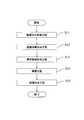
- FIG. 6 is a flowchart showing a method for manufacturing a capacitor element according to an embodiment of the present invention.
- FIG. 7 is a flowchart showing a method for manufacturing a capacitor element according to another embodiment of the present invention.
- FIG. 8 is a flowchart showing a method for manufacturing an electrolytic capacitor according to an embodiment of the present invention.
- Capacitor element In order to increase the capacitance, a porous region is usually formed on the surface of the anode body.
- a larger void may be formed in the porous region. Therefore, the electric resistance in the anode portion becomes large, and the ESR tends to increase. Further, the strength of the capacitor element in the welded portion may decrease.
- oxygen that has entered from the anode portion easily reaches the cathode forming portion through the void, and the deterioration of the solid electrolyte layer progresses.
- the porous region in the anode portion is thinned to form a thin-walled region, and a dense metal base material is laminated on a part thereof.
- a cathode layer (for example, a solid electrolyte layer and a cathode extraction layer) is formed in the cathode forming portion of the anode body. Therefore, the thickness of the cathode forming portion of the capacitor element is larger than that of the anode portion.
- the anode body is bent in the vicinity of the boundary between the anode portion and the cathode layer. Therefore, the anode body is easily damaged at the bent portion. If a thin region is provided in the anode portion, the degree of this bending is further increased.
- the metal base material is laminated on at least a part of the thin-walled region, a plurality of capacitor elements can be laminated and joined without increasing the degree of bending.
- the thickness of the porous region may be 95% or more of the thickness of the entire anode body. From the viewpoint of strength, the thickness of the porous region in the cathode forming portion is preferably 98% or less of the thickness of the entire anode body.
- the thin-walled region may be formed in a part of the anode part. From the viewpoint of oxygen blocking, the thin-walled region is preferably formed in a band shape in the direction along the boundary between the anode portion and the cathode forming portion. It is more preferable that the thin-walled region is formed in a band shape in the vicinity of the boundary between the anode portion and the cathode forming portion. This is because the thin-walled region makes it easier to prevent the solid electrolyte from penetrating into the anode side in the step of forming the solid electrolyte layer.
- the thin-walled region may be formed over the entire anode portion.
- the thin-walled region may be formed by removing a part of the porous region, or may be formed by compressing a part of the porous region. Above all, it is preferable that a thin-walled region is formed by compressing the porous region. By compressing the porous region, a compression layer having a smaller porosity is formed in the thin-walled region, so that the effect of suppressing electrical resistance and the effect of suppressing oxygen transfer are further enhanced.
- a metal base material is laminated on at least a part of the thin-walled area.
- the portion where the metal base material is laminated is suitable as a welded portion.
- the metal base material is preferably laminated in a band shape in the direction along the boundary between the anode portion and the cathode forming portion. From the viewpoint of strength, it is preferable that the metal base material is laminated over the entire thin-walled region.
- the capacitor element according to the present embodiment includes an island-shaped thin-walled region in the planned welding portion of the anode portion.
- the area of the thin-walled region is, for example, 3% or more and less than 10% of the area of the anode portion.
- the metal substrate is laminated over the entire thin area. As a result, the increase in electrical resistance due to welding is suppressed. Furthermore, the movement of oxygen is likely to be suppressed.
- FIG. 1A is a top view schematically showing a capacitor element according to this embodiment.
- FIG. 1B is a cross-sectional view schematically showing a capacitor element cut along the line XX of FIG. 1A.
- the capacitor element 110 is, for example, in the form of a sheet.
- the capacitor element 110 includes an anode body 11, a dielectric layer 12 that covers at least a part of the anode body 11, and a cathode layer 13 that covers at least a part of the dielectric layer.
- the cathode layer 13 includes a solid electrolyte layer 131 and a cathode extraction layer 132 that covers at least a part of the solid electrolyte layer 131.
- the anode body 11 includes an anode portion 11a and a cathode forming portion 11b. Porous regions 11X are arranged on both main surface sides of the anode body 11. A core region 11Y is interposed between the two porous regions 11X. The thickness of the core region 11Y may be even smaller.
- Two island-shaped thin-walled regions are formed in a part of the anode portion 11a.
- the thickness of the porous region 11X in the thin-walled region is thinner than that of the porous region 11X in the cathode forming portion 11b.
- the metal base material 20 is laminated on the entire thin-walled region. In the thin region, a plurality of capacitor elements 110 are welded.
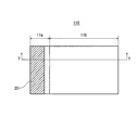
- the capacitor element according to the present embodiment is arranged at the end of the anode portion and includes a thin-walled region formed in a band shape in the direction along the boundary between the anode portion and the cathode forming portion.
- the area of the thin-walled region is, for example, 10% or more and less than 50% of the area of the anode portion.
- the metal substrate is laminated over the entire thin area. As a result, the increase in electrical resistance due to welding is suppressed. Furthermore, the movement of oxygen is likely to be suppressed. In addition, the strength of the capacitor element is increased.
- FIG. 2 is a top view schematically showing a capacitor element according to the present embodiment.
- the present embodiment has the same configuration as that of the first embodiment except that a strip-shaped thin-walled region is formed at the end of the anode portion 11a.
- the metal base material 20 is laminated over the entire thin-walled region.
- the capacitor element according to this embodiment has a cross section similar to that in FIG. 1B.
- the capacitor element according to the present embodiment is arranged at the end of the anode portion and includes a thin-walled region formed in a band shape in the direction along the boundary between the anode portion and the cathode forming portion.
- the thin-walled region in the present embodiment is wider than the thin-walled region in the second embodiment. Therefore, when a plurality of capacitor elements are laminated, the capacitor elements are bent at a portion including a thin-walled region.
- the area of the thin-walled region is, for example, 50% or more and less than 80% of the area of the anode portion.
- the metal substrate is laminated over the entire thin area. As a result, the increase in electrical resistance due to welding is suppressed. Furthermore, the movement of oxygen is likely to be suppressed. In addition, the strength of the capacitor element is further increased.
- FIG. 3A is a top view schematically showing the capacitor element according to the present embodiment.
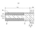
- FIG. 3B is a cross-sectional view schematically showing a capacitor element cut along the YY line of FIG. 3A.
- This embodiment has the same configuration as that of the first embodiment except that a strip-shaped thin-walled region is formed in a part including the end portion of the anode portion 11a.
- the metal base material 20 is laminated over the entire thin-walled region.
- the capacitor element according to the present embodiment includes a thin-walled region in the entire anode portion.
- the thin-walled region is formed over the entire anode portion.
- the metal substrate is laminated over the entire thin area.
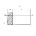
- FIG. 4A is a top view schematically showing the capacitor element according to the present embodiment.
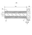
- FIG. 4B is a cross-sectional view schematically showing a capacitor element cut along the line ZZ of FIG. 4A.
- This embodiment has the same configuration as that of the first embodiment except that a thin-walled region is formed on the entire anode portion 11a.
- the metal base material 20 is laminated over the entire thin-walled region.
- the thin-walled region is formed in at least a part of the anode portion.
- the porous region in the thin-walled region is thinner than the porous region in the cathode forming portion. Therefore, it is difficult for oxygen that has entered from the anode portion to reach the cathode forming portion beyond the thin-walled region.
- the thin-walled region also has a role of preventing the solid electrolyte from permeating to the anode side through the porous region of the cathode forming portion in the step of forming the solid electrolyte layer.
- the thickness of the porous region in the thin region is not particularly limited.
- the thickness of the porous region in the thin-walled region is preferably 50% or less, preferably 40% or less, and preferably 30% or less of the thickness of the porous region in the cathode forming portion. There may be no porous region in the thin region.
- the thickness of the porous region in the thin-walled region is arbitrary in the cross section of the capacitor element from one main surface of the anode in the thin-walled region to the boundary between the porous region and the core region formed on the main surface side. It is the average value of the distances of three points.
- the thickness of the porous region in the cathode forming portion is also any three points from one main surface of the anode body in the cathode forming portion to the boundary between the porous region and the core region formed on the main surface side. Is the average value of the distances.
- the thin-walled region is formed by, for example, compressing the porous region of the anode body.
- the thin-walled region has a compressed layer in which the porous region is compressed.
- the thin-walled region may be formed by removing at least a part of the porous region by cutting, laser processing, or the like.
- the thin-walled region may be formed by removing the entire porous region and exposing the core region.
- the thin-walled region is preferably formed by compressing the porous region of the anode body. This is because the process is simple and further improvement in oxygen blocking property can be expected.
- the metal substrate is laminated on at least a part of the thin area.
- the metal substrate is denser than the porous region in the cathode forming portion.
- the fact that the metal base material is dense is synonymous with the fact that the apparent density of the metal base material is higher than the apparent density of the porous region in the cathode forming portion.
- the apparent density is calculated by dividing the actual mass by the apparent volume including the void portion.
- the porosity of the metal base material is synonymous with the porosity of the metal base material being smaller than the porosity of the porous region in the cathode forming portion.
- the porosity of the metal substrate may be, for example, 90% or less, 80% or less, or 60% or less of the porosity of the porous region in the cathode forming portion.
- the metal base material does not have to have holes inside.
- the porosity of the metal substrate is not particularly limited.
- the porosity of the metal substrate may be, for example, 0% or more and 55% or less.
- Porosity can be calculated from an SEM image of a cross section of a capacitor element cut in the thickness direction.
- the porous region in the cathode forming portion of the SEM image is binarized between the void portion and the other portion, and the area ratio of the void portion in the porous region is calculated.
- the area ratio of the obtained void portion is defined as the porosity of the porous region in the cathode forming portion.
- the area ratio of the void portion in the metal base material is calculated from the SEM image, and the area ratio of the obtained void portion is defined as the porosity of the metal base material.
- the metal base material is a plate-shaped or foil-shaped member containing a metal material.
- the thickness of the metal base material is not particularly limited.
- the total thickness of the metal base material and the anode body in the thin-walled region may be smaller, larger, or the same as the thickness of the anode body in the cathode forming portion.
- the total thickness is preferably equal to or larger than the thickness of the anode body in the cathode forming portion in that a plurality of capacitor elements are easily welded.
- the total thickness is preferably about 100% or more and 120% or less of the thickness of the anode body in the cathode forming portion.
- the metal material constituting the metal base material is not particularly limited.
- the metal base material preferably contains the same metal material as the anode or the valve acting metal. In this case, the electrical resistance between the anode and the metal base material, the ease of welding, and the like are about the same, so that the connection reliability is not impaired.
- the surface of the laminated metal base material facing the thin region (hereinafter, may be referred to as a facing surface) is roughened. This is because the adhesion with the porous region is enhanced.
- the roughness of the facing surface is not particularly limited.
- the arithmetic mean roughness Ra of the facing surfaces may be, for example, 20 nm or more.
- the arithmetic mean roughness Ra is measured according to JIS B 0601: 2013.
- the metal substrate may have a porous region on its surface.
- the surface of the metal base material opposite to the facing surface may be roughened.
- the roughening method is not particularly limited.
- the facing surface may be etched or roughened by a conventionally known surface treatment such as plasma treatment or blast treatment.
- the anode body includes a foil (metal foil) containing a valve acting metal.
- the valve acting metal include titanium, tantalum, aluminum and niobium.
- the anode contains one or more of the above valvular metals.
- the anode body may contain the above-mentioned valve acting metal in the form of an alloy or an intermetallic compound.
- the thickness of the anode body is not particularly limited. The thickness of the anode body other than the thin-walled region may be, for example, 15 ⁇ m or more and 300 ⁇ m or less, and 80 ⁇ m or more and 250 ⁇ m or less.
- the anode body includes a porous region formed on the main surface side thereof.
- the entire anode may be porous.
- the anode body includes a porous region arranged on both main surface sides and a core region having a lower porosity, which is interposed between the porous regions.
- the porous region is a region having a large number of fine pores.
- the core region is, for example, a region that has not been electrolytically etched.
- the porous region and the core region can be distinguished from the cross section of the capacitor element.
- the porosity of the porous region is not particularly limited.
- the porosity of the porous region may be, for example, 35% or more and 65% or less.
- the thickness of the porous region is not particularly limited. As described above, from the viewpoint of capacitance and strength, the thickness of the porous region in the cathode forming portion is preferably 95% or more and 98% or less of the thickness of the entire anode body.
- the dielectric layer is formed on at least a portion of the surface of the anode.
- the dielectric layer is formed by, for example, anodizing the surface of the anode body by chemical conversion treatment or the like. Therefore, the dielectric layer may contain oxides of the valvening metal.
- the dielectric layer may contain Al 2 O 3.
- the dielectric layer is not limited to this, and may be any one that functions as a dielectric.
- the cathode layer includes a solid electrolyte layer that covers at least a part of the dielectric layer, and a cathode extraction layer that covers at least a part of the solid electrolyte layer.
- the solid electrolyte layer may be formed so as to cover at least a part of the dielectric layer, and may be formed so as to cover the entire surface of the dielectric layer.
- the solid electrolyte layer contains, for example, a manganese compound and a conductive polymer.
- the conductive polymer include polypyrrole, polythiophene, polyfuran, polyaniline, polyacetylene, polyphenylene, polyphenylene vinylene, polyacene, polythiophene vinylene and the like. These may be used alone, in combination of two or more, or in a copolymer of two or more monomers.
- polypyrrole, polythiophene, polyfuran, polyaniline, etc. mean macromolecules having polypyrrole, polythiophene, polyfuran, polyaniline, etc. as the basic skeleton, respectively. Therefore, polypyrrole, polythiophene, polyfuran, polyaniline and the like may also contain their respective derivatives.
- polythiophene includes poly (3,4-ethylenedioxythiophene) and the like.
- the conductive polymer may be contained in the solid electrolyte layer together with the dopant.
- the dopant may be a monomolecular anion or a polymer anion.
- the monomolecular anion include paratoluenesulfonic acid and naphthalenesulfonic acid.
- Specific examples of the high molecular weight anion include polyvinyl sulfonic acid, polystyrene sulfonic acid, polyallyl sulfonic acid, polyacrylic sulfonic acid, polymethacrylic sulfonic acid, poly (2-acrylamide-2-methylpropanesulfonic acid), and polyisoprene sulfonic acid. , Polyacrylic acid and the like.
- These may be used alone or in combination of two or more. Further, these may be polymers of a single monomer or may be a copolymer of two or more kinds of monomers. Of these, a polymer anion derived from polystyrene sulfonic acid is preferable.
- the cathode extraction layer may be formed so as to cover at least a part of the solid electrolyte layer, and may be formed so as to cover the entire surface of the solid electrolyte layer.
- the cathode extraction layer has, for example, a carbon layer and a metal (for example, silver) paste layer formed on the surface of the carbon layer.
- the carbon layer is composed of a carbon paste containing a conductive carbon material such as graphite.
- the metal paste layer is composed of, for example, a composition containing silver particles and a resin.
- the structure of the cathode extraction layer is not limited to this, and may be any structure having a current collecting function.
- the electrolytic capacitor according to this embodiment includes the above-mentioned capacitor element.
- the electrolytic capacitor may include a plurality of capacitor elements.
- a plurality of capacitor elements are laminated.
- the number of laminated capacitor elements is not particularly limited, and is, for example, 2 or more and 20 or less.
- At least one of the plurality of capacitor elements may be the capacitor element according to the present embodiment. Others may be conventionally known capacitor elements. Preferably, all of the plurality of capacitor elements arranged in the electrolytic capacitor are the capacitor elements according to the present embodiment.
- the anode parts of the laminated capacitor elements are joined by welding and electrically connected. According to the present embodiment, since the laminated capacitor element is welded at the portion where the metal base material is laminated, the occupancy ratio of the void formed by welding becomes small, or the void itself becomes small. Therefore, the increase in electrical resistance at the anode portion is suppressed.
- the plurality of anode portions may be welded after being crimped by, for example, bent anode lead terminals.
- the anode lead terminal is joined to the anode part of at least one capacitor element.
- the portion of the anode portion on which the metal base material is laminated may be welded to the anode lead terminal.
- the cathode layers of the laminated capacitor elements are also electrically connected to each other.
- a cathode lead terminal is bonded to the cathode layer of at least one capacitor element.
- the cathode lead terminals are joined via a conductive adhesive or solder, or by resistance welding or laser welding.
- the conductive adhesive is, for example, a mixture of a curable resin and carbon particles or metal particles.
- the material of the lead terminal is not particularly limited as long as it is electrochemically and chemically stable and has conductivity, and may be metal or non-metal.
- the shape is also not particularly limited.
- the thickness of the lead terminal (distance between the main surfaces of the lead terminal) is preferably 25 ⁇ m or more and 200 ⁇ m or less, and more preferably 25 ⁇ m or more and 100 ⁇ m or less from the viewpoint of reducing the height.
- the capacitor element may be sealed with a sealing resin so that at least a part of the anode lead terminal and the cathode lead terminal is exposed.
- sealing resin examples include cured products of curable resins and engineering plastics.
- thermosetting resin examples include epoxy resin, phenol resin, silicone resin, melamine resin, urea resin, alkyd resin, polyurethane, and unsaturated polyester.
- Engineering plastics include general purpose engineering plastics and super engineering plastics. Examples of engineering plastics include polyimide and polyamide-imide.
- FIG. 5 is a cross-sectional view schematically showing the electrolytic capacitor according to the present embodiment.
- the electrolytic capacitor 100 includes one or more capacitor elements 110, an anode lead terminal 120A bonded to the anode portion 11a, a cathode lead terminal 120B bonded to the cathode layer 13, and a sealing resin 130 that seals the capacitor element 110. And.
- the capacitor element according to this embodiment can be manufactured by the following method.
- the present embodiment includes a method for manufacturing a capacitor element.
- the method for manufacturing a capacitor element according to the present embodiment includes a preparatory step of preparing an anode having a porous region on the surface, a dielectric layer forming step of forming a dielectric layer covering at least a part of the anode, and porous. Except for the thin-walled region forming step of forming a thin-walled region on the anode by compressing or removing a part of the quality region, the laminating step of laminating a metal base material on at least a part of the thin-walled region, and the thin-walled region of the anode body.
- a cathode forming step of forming a cathode layer is provided in the portion of.
- the laminated metal substrate is denser than the porous region in the cathode forming portion.
- FIG. 6 is a flowchart showing a method of manufacturing a capacitor element according to the present embodiment.
- FIG. 7 is a flowchart showing another method for manufacturing a capacitor element according to the present embodiment.
- Preparation step (S11) As a raw material for the anode body, for example, a metal foil containing a valve acting metal is used. Roughen at least one main surface of the metal leaf. By roughening, a porous region having a large number of fine pores is formed at least on the main surface side of the metal foil.
- Electrolytic etching is performed, for example, by electrolytic etching a metal foil.
- Electrolytic etching can be performed by, for example, a DC electrolysis method or an AC electrolysis method.
- the etching conditions are not particularly limited, and are appropriately set according to the depth of the porous region, the type of valve acting metal, and the like.
- Dielectric layer forming step (S12) A dielectric layer is formed on the surface of the anode body.
- the method for forming the dielectric layer is not particularly limited.
- the dielectric layer can be formed, for example, by chemical conversion treatment of the anode body.
- the chemical conversion treatment for example, the anode is immersed in a chemical conversion solution such as an ammonium adipate solution and heat-treated.
- the anode body may be immersed in a chemical conversion solution and a voltage may be applied.
- the porous region can be compressed by pressing the anode forming portion.
- the removal of the porous region can be performed by cutting the porous region of the anode forming portion.
- a metal substrate is laminated on at least a part of the thin area. After laminating, the laminated portion of the metal base material and the anode body may be pressed to bring the metal base material and the anode body into close contact with each other.
- a metal foil having a porosity similar to that of the anode can be used as the metal base material.
- the pressing after laminating compresses the porous region of the metal base material, and the metal base material is densified.
- the metal substrate to be laminated may be etched in the same manner as the anode body. The surface of the metal substrate to be laminated may be roughened.
- the laminating step (4) is performed following the thin-walled region forming step (3) or in parallel with the thin-walled region forming step (3). Above all, it is preferable that the thin-walled region forming step (3) and the laminating step (4) are performed in parallel (see FIG. 7).
- a metal base material is arranged so as to cover a part of the porous region, and the laminated portion of the metal base material and the anode body is pressed. As a result, the porous region is compressed to form a thin-walled region, and the metal base material is laminated on the thin-walled region. At the same time, the metal substrate and the anode are crimped. According to this method, the man-hours can be reduced, and further, it becomes easy to arrange the metal base material in the thin-walled region.
- a solid electrolyte layer is formed on the surface of the dielectric layer.
- the solid electrolyte layer can be formed by chemically and / or electrolytically polymerizing the raw material monomer or oligomer in the presence of the anode.
- the solid electrolyte layer may be formed by applying a solution in which the conductive polymer is dissolved or a dispersion liquid in which the conductive polymer is dispersed to the dielectric layer.
- the raw material monomer or oligomer is a monomer or oligomer that is a raw material for the conductive polymer.
- a monomer or oligomer that is a raw material for the conductive polymer.
- pyrrole, aniline, thiophene, derivatives thereof and the like for example, pyrrole, aniline, thiophene, derivatives thereof and the like.
- the polymerization solution used for chemical polymerization and / or electrolytic polymerization may contain the above-mentioned dopant in addition to the raw material monomer or oligomer.
- a carbon paste and a silver paste are sequentially applied to the surface of the solid electrolyte layer to form a cathode extraction layer.
- a cathode layer is formed and a capacitor element is obtained.
- the thin-walled region forming step (3) and the laminating step (4) may be performed before the dielectric layer forming step (2) or after the cathode forming step (5).
- the thin-walled region forming step (3) and the laminating step (4) are carried out before the dielectric layer forming step (2). Since the anode body is reinforced by the metal base material, damage to the anode body during transportation can be easily suppressed.
- the thin-walled region forming step (3) and the laminating step (4) are preferably performed after the cathode forming step (5) in that the influence on the subsequent steps is reduced.
- the electrolytic capacitor according to this embodiment can be manufactured by the following method.
- the present embodiment includes a method for manufacturing an electrolytic capacitor.
- the method for manufacturing an electrolytic capacitor according to the present embodiment includes a step of preparing a capacitor element manufactured by the above method and a joining step of laminating a plurality of capacitor elements and welding the anode portions to each other.
- FIG. 8 is a flowchart showing a method for manufacturing an electrolytic capacitor according to the present embodiment.
- At least one of the plurality of capacitor elements may be the capacitor element according to the present embodiment. Others may be conventionally known capacitor elements. Preferably, two or more of the plurality of capacitor elements arranged in the electrolytic capacitor are the capacitor elements according to the present embodiment. In this case, the thin-walled regions are welded together with the metal base material.
- the welding method is not particularly limited, and any method can obtain the effect of the present embodiment.
- Examples of the welding method include laser welding, resistance welding, arc welding, gas welding, electron beam welding and brazing.
- Laser welding is a method of irradiating laser light to melt and join metals.
- Resistance welding is a method of melting and joining metals using Joule heat generated by energization.
- Arc welding is a method of melting and joining metals by utilizing the phenomenon of electric discharge in air.
- Gas welding is a method of melting and joining metals using flammable gas.
- Electron beam welding is a method of melting and joining metals by colliding electrons emitted in a vacuum.
- Brazing is a method of joining by interposing a brazing material having a melting point lower than that of the base material (in this case, a metal base material or an anode).
- (Iii) Lead terminal connection step (S3) The anode lead terminal is electrically connected to the anode portion, and the cathode lead terminal is electrically connected to the cathode layer.
- the electrical connection between the anode portion and the anode lead terminal is performed, for example, by welding these by the above method.
- the electrical connection between the cathode layer and the cathode lead terminal is performed, for example, by adhering the cathode layer and the cathode lead terminal via a conductive adhesive.
- Sealing step (S4) A part of the capacitor element and the lead terminal may be sealed with a sealing resin. Sealing is performed using molding techniques such as injection molding, insert molding, and compression molding. For example, using a predetermined mold, a composition containing a curable resin or a thermoplastic resin is filled so as to cover one end of a capacitor element and a lead terminal, and then heating or the like is performed.
- the ESR of the electrolytic capacitor according to the above aspect of the present invention is reduced. Therefore, it can be used for electrolytic capacitors for various purposes that require low ESR.
- Electrolytic capacitor 110 Capacitor element 11: Anode body 11X: Porous region 11Y: Core region 11a: Anode portion 11b: Cathode forming portion 12: Dielectric layer 13: Cathode layer 131: Solid electrolyte layer 132: Cathode extraction layer 20 : Metal substrate 120A: Anode lead terminal 120B: Cathode lead terminal 130: Encapsulating resin
Landscapes
- Engineering & Computer Science (AREA)
- Power Engineering (AREA)
- Microelectronics & Electronic Packaging (AREA)
- Manufacturing & Machinery (AREA)
- Fixed Capacitors And Capacitor Manufacturing Machines (AREA)
Priority Applications (3)
| Application Number | Priority Date | Filing Date | Title |
|---|---|---|---|
| US17/756,766 US12154728B2 (en) | 2019-12-25 | 2020-12-22 | Capacitor element, electrolytic capacitor, and methods for manufacturing same |
| CN202080087524.2A CN114868216B (zh) | 2019-12-25 | 2020-12-22 | 电容器元件及电解电容器、以及它们的制造方法 |
| JP2021567479A JPWO2021132220A1 (https=) | 2019-12-25 | 2020-12-22 |
Applications Claiming Priority (2)
| Application Number | Priority Date | Filing Date | Title |
|---|---|---|---|
| JP2019235136 | 2019-12-25 | ||
| JP2019-235136 | 2019-12-25 |
Publications (1)
| Publication Number | Publication Date |
|---|---|
| WO2021132220A1 true WO2021132220A1 (ja) | 2021-07-01 |
Family
ID=76574685
Family Applications (1)
| Application Number | Title | Priority Date | Filing Date |
|---|---|---|---|
| PCT/JP2020/047883 Ceased WO2021132220A1 (ja) | 2019-12-25 | 2020-12-22 | コンデンサ素子および電解コンデンサ、ならびにこれらの製造方法 |
Country Status (4)
| Country | Link |
|---|---|
| US (1) | US12154728B2 (https=) |
| JP (1) | JPWO2021132220A1 (https=) |
| CN (1) | CN114868216B (https=) |
| WO (1) | WO2021132220A1 (https=) |
Cited By (1)
| Publication number | Priority date | Publication date | Assignee | Title |
|---|---|---|---|---|
| WO2023190050A1 (ja) * | 2022-03-29 | 2023-10-05 | 株式会社村田製作所 | 固体電解コンデンサ |
Citations (2)
| Publication number | Priority date | Publication date | Assignee | Title |
|---|---|---|---|---|
| WO2007069670A1 (ja) * | 2005-12-15 | 2007-06-21 | Showa Denko K. K. | コンデンサチップ及びその製造方法 |
| WO2013046869A1 (ja) * | 2011-09-26 | 2013-04-04 | 株式会社村田製作所 | 固体電解コンデンサおよびその製造方法 |
Family Cites Families (13)
| Publication number | Priority date | Publication date | Assignee | Title |
|---|---|---|---|---|
| JPH05205984A (ja) * | 1992-01-27 | 1993-08-13 | Nec Corp | 積層型固体電解コンデンサ |
| JP2004088073A (ja) | 2002-06-07 | 2004-03-18 | Matsushita Electric Ind Co Ltd | 固体電解コンデンサ |
| US6791822B2 (en) | 2002-06-07 | 2004-09-14 | Matsushita Electric Industrial Co., Ltd. | Solid electrolytic capacitor |
| JP2004095816A (ja) * | 2002-08-30 | 2004-03-25 | Matsushita Electric Ind Co Ltd | チップ形コンデンサ |
| JP4149891B2 (ja) * | 2002-12-27 | 2008-09-17 | 松下電器産業株式会社 | コンデンサとコンデンサ内蔵回路基板、ならびにそれらの製造方法 |
| JPWO2006129639A1 (ja) * | 2005-05-31 | 2009-01-08 | 昭和電工株式会社 | 固体電解コンデンサ及びその製造方法 |
| US7848083B2 (en) * | 2005-06-23 | 2010-12-07 | Murata Manufacturing Co., Ltd. | Solid electrolytic capacitor and method for manufacturing same |
| US8213158B2 (en) * | 2007-09-28 | 2012-07-03 | Sanyo Electric Co., Ltd. | Solid electrolytic capacitor and its production method |
| JP2011049390A (ja) * | 2009-08-27 | 2011-03-10 | Tdk Corp | 積層型電解コンデンサ |
| JP2013131627A (ja) * | 2011-12-21 | 2013-07-04 | Nec Tokin Corp | 固体電解コンデンサ及びその製造方法 |
| JP6641915B2 (ja) * | 2015-11-18 | 2020-02-05 | 株式会社村田製作所 | 固体電解コンデンサ |
| CN111149182B (zh) * | 2017-09-28 | 2022-07-29 | 松下知识产权经营株式会社 | 电解电容器及其制造方法 |
| US11862406B2 (en) * | 2019-01-24 | 2024-01-02 | Panasonic Intellectual Property Management Co., Ltd. | Solid electrolytic capacitor and method for manufacturing same |
-
2020
- 2020-12-22 WO PCT/JP2020/047883 patent/WO2021132220A1/ja not_active Ceased
- 2020-12-22 US US17/756,766 patent/US12154728B2/en active Active
- 2020-12-22 JP JP2021567479A patent/JPWO2021132220A1/ja active Pending
- 2020-12-22 CN CN202080087524.2A patent/CN114868216B/zh active Active
Patent Citations (2)
| Publication number | Priority date | Publication date | Assignee | Title |
|---|---|---|---|---|
| WO2007069670A1 (ja) * | 2005-12-15 | 2007-06-21 | Showa Denko K. K. | コンデンサチップ及びその製造方法 |
| WO2013046869A1 (ja) * | 2011-09-26 | 2013-04-04 | 株式会社村田製作所 | 固体電解コンデンサおよびその製造方法 |
Cited By (1)
| Publication number | Priority date | Publication date | Assignee | Title |
|---|---|---|---|---|
| WO2023190050A1 (ja) * | 2022-03-29 | 2023-10-05 | 株式会社村田製作所 | 固体電解コンデンサ |
Also Published As
| Publication number | Publication date |
|---|---|
| US12154728B2 (en) | 2024-11-26 |
| CN114868216A (zh) | 2022-08-05 |
| JPWO2021132220A1 (https=) | 2021-07-01 |
| US20230005671A1 (en) | 2023-01-05 |
| CN114868216B (zh) | 2025-02-25 |
Similar Documents
| Publication | Publication Date | Title |
|---|---|---|
| JP7576746B2 (ja) | 電解コンデンサおよびその製造方法 | |
| US6473293B2 (en) | Capacitor unit, method for producing the same, and solid electrolytic capacitor | |
| JP7489624B2 (ja) | 電解コンデンサおよびその製造方法 | |
| CN108140493B (zh) | 固体电解电容器以及固体电解电容器的制造方法 | |
| CN101471185B (zh) | 漏电流小的固体电解电容器及其制造方法 | |
| JP2003133183A (ja) | 固体電解コンデンサおよびその製造方法 | |
| CN115885358B (zh) | 固体电解电容器元件及固体电解电容器 | |
| CN111755253A (zh) | 固体电解电容器及固体电解电容器的制造方法 | |
| CN114600208A (zh) | 电解电容器 | |
| JP7029666B2 (ja) | 固体電解コンデンサ | |
| CN114868216B (zh) | 电容器元件及电解电容器、以及它们的制造方法 | |
| JP2004088073A (ja) | 固体電解コンデンサ | |
| US12340955B2 (en) | Solid electrolytic capacitor element having improved thermal stability, and solid electrolytic capacitor and method for manufacturing same | |
| CN103531361B (zh) | 固体电解电容器及其制造方法 | |
| US20220122779A1 (en) | Electrolytic capacitor and method for producing same | |
| JP2007180328A (ja) | 積層型固体電解コンデンサおよびコンデンサモジュール | |
| JP2008300738A (ja) | 積層型固体電解コンデンサ | |
| JP2008205072A (ja) | 固体電解コンデンサ及びその製造方法 | |
| JP2022039775A (ja) | 固体電解コンデンサ素子および固体電解コンデンサ |
Legal Events
| Date | Code | Title | Description |
|---|---|---|---|
| 121 | Ep: the epo has been informed by wipo that ep was designated in this application |
Ref document number: 20904426 Country of ref document: EP Kind code of ref document: A1 |
|
| ENP | Entry into the national phase |
Ref document number: 2021567479 Country of ref document: JP Kind code of ref document: A |
|
| NENP | Non-entry into the national phase |
Ref country code: DE |
|
| 122 | Ep: pct application non-entry in european phase |
Ref document number: 20904426 Country of ref document: EP Kind code of ref document: A1 |
|
| WWG | Wipo information: grant in national office |
Ref document number: 202080087524.2 Country of ref document: CN |