WO2021125228A1 - チューニング調整回路を有するワイヤレス給電システム - Google Patents
チューニング調整回路を有するワイヤレス給電システム Download PDFInfo
- Publication number
- WO2021125228A1 WO2021125228A1 PCT/JP2020/046981 JP2020046981W WO2021125228A1 WO 2021125228 A1 WO2021125228 A1 WO 2021125228A1 JP 2020046981 W JP2020046981 W JP 2020046981W WO 2021125228 A1 WO2021125228 A1 WO 2021125228A1
- Authority
- WO
- WIPO (PCT)
- Prior art keywords
- power
- feeding
- resonance
- coil
- power supply
- Prior art date
- Legal status (The legal status is an assumption and is not a legal conclusion. Google has not performed a legal analysis and makes no representation as to the accuracy of the status listed.)
- Ceased
Links
Images







Classifications
-
- H—ELECTRICITY
- H02—GENERATION; CONVERSION OR DISTRIBUTION OF ELECTRIC POWER
- H02J—ELECTRIC POWER NETWORKS; CIRCUIT ARRANGEMENTS OR SYSTEMS FOR SUPPLYING OR DISTRIBUTING ELECTRIC POWER; SYSTEMS FOR STORING ELECTRIC ENERGY
- H02J50/00—Circuit arrangements or systems for wireless supply or distribution of electric power
- H02J50/10—Circuit arrangements or systems for wireless supply or distribution of electric power using inductive coupling
- H02J50/12—Circuit arrangements or systems for wireless supply or distribution of electric power using inductive coupling of the resonant type
-
- H—ELECTRICITY
- H02—GENERATION; CONVERSION OR DISTRIBUTION OF ELECTRIC POWER
- H02J—ELECTRIC POWER NETWORKS; CIRCUIT ARRANGEMENTS OR SYSTEMS FOR SUPPLYING OR DISTRIBUTING ELECTRIC POWER; SYSTEMS FOR STORING ELECTRIC ENERGY
- H02J50/00—Circuit arrangements or systems for wireless supply or distribution of electric power
- H02J50/40—Circuit arrangements or systems for wireless supply or distribution of electric power using two or more transmitting or receiving devices
-
- H—ELECTRICITY
- H02—GENERATION; CONVERSION OR DISTRIBUTION OF ELECTRIC POWER
- H02J—ELECTRIC POWER NETWORKS; CIRCUIT ARRANGEMENTS OR SYSTEMS FOR SUPPLYING OR DISTRIBUTING ELECTRIC POWER; SYSTEMS FOR STORING ELECTRIC ENERGY
- H02J50/00—Circuit arrangements or systems for wireless supply or distribution of electric power
- H02J50/40—Circuit arrangements or systems for wireless supply or distribution of electric power using two or more transmitting or receiving devices
- H02J50/402—Circuit arrangements or systems for wireless supply or distribution of electric power using two or more transmitting or receiving devices the two or more transmitting or the two or more receiving devices being integrated in the same unit, e.g. power mats with several coils or antennas with several sub-antennas
-
- H—ELECTRICITY
- H02—GENERATION; CONVERSION OR DISTRIBUTION OF ELECTRIC POWER
- H02J—ELECTRIC POWER NETWORKS; CIRCUIT ARRANGEMENTS OR SYSTEMS FOR SUPPLYING OR DISTRIBUTING ELECTRIC POWER; SYSTEMS FOR STORING ELECTRIC ENERGY
- H02J50/00—Circuit arrangements or systems for wireless supply or distribution of electric power
- H02J50/60—Circuit arrangements or systems for wireless supply or distribution of electric power responsive to the presence of foreign objects, e.g. detection of living beings
-
- H—ELECTRICITY
- H02—GENERATION; CONVERSION OR DISTRIBUTION OF ELECTRIC POWER
- H02J—ELECTRIC POWER NETWORKS; CIRCUIT ARRANGEMENTS OR SYSTEMS FOR SUPPLYING OR DISTRIBUTING ELECTRIC POWER; SYSTEMS FOR STORING ELECTRIC ENERGY
- H02J50/00—Circuit arrangements or systems for wireless supply or distribution of electric power
- H02J50/80—Circuit arrangements or systems for wireless supply or distribution of electric power involving the exchange of data, concerning supply or distribution of electric power, between transmitting devices and receiving devices
-
- H—ELECTRICITY
- H02—GENERATION; CONVERSION OR DISTRIBUTION OF ELECTRIC POWER
- H02J—ELECTRIC POWER NETWORKS; CIRCUIT ARRANGEMENTS OR SYSTEMS FOR SUPPLYING OR DISTRIBUTING ELECTRIC POWER; SYSTEMS FOR STORING ELECTRIC ENERGY
- H02J50/00—Circuit arrangements or systems for wireless supply or distribution of electric power
- H02J50/90—Circuit arrangements or systems for wireless supply or distribution of electric power involving detection or optimisation of position, e.g. alignment
-
- H—ELECTRICITY
- H03—ELECTRONIC CIRCUITRY
- H03H—IMPEDANCE NETWORKS, e.g. RESONANT CIRCUITS; RESONATORS
- H03H7/00—Multiple-port networks comprising only passive electrical elements as network components
- H03H7/01—Frequency selective two-port networks
- H03H7/0115—Frequency selective two-port networks comprising only inductors and capacitors
Definitions
- the present invention relates to wireless power feeding, particularly wireless power feeding in which power is supplied by inductive coupling of a resonance method.
- the method using electromagnetic induction is widely and generally known.
- the method using the technique of resonance by electromagnetic induction is typical and is called by various names.
- the present invention presupposes a technique using magnetic coupling using an LC resonant circuit.
- Patent Document 1 discloses a wireless power supply method and a power supply system that enable the use of a wider range of frequencies to be expanded in wireless power supply that can supply power to a relatively long distance by coupling by electromagnetic field resonance.
- the electromagnetic resonance wireless power supply method is a wireless power supply in which the power transmission circuit of the power transmission device and the power reception circuit of the power reception device are coupled by electromagnetic resonance, and the power transmission device is connected to the power supply 2 with two different frequency components f1 and f2.
- the resonance frequency of the power transmission circuit is set to f1 and / or f2, the conditions of the power transmission circuit are changed periodically to create an electrical transient state in which the current or voltage is not stable, and the power receiving device is set to the resonance frequency of the power receiving circuit.
- the load is supplied with power according to the frequency of (f2-f1) or (f1 + f2).
- Patent Document 2 discloses a very simple wireless power supply using a loop coil as a power transmission device.
- the power transmission loop coil provided in the power transmission device extracts electrical energy from the DC power source and generates cyclically changing electromagnetic field resonance energy in the space.
- the power receiving loop coil provided in the power receiving device extracts the electromagnetic field resonance energy that changes periodically as electric energy from the space and supplies electric power to the load.
- the power transmission loop coil and the power reception loop coil are electromagnetically resonantly coupled, and power is wirelessly supplied from the power transmission device to the power receiver.
- Patent Document 3 discloses a wireless power supply system including a plurality of relay devices, which suppresses a decrease in power transmission efficiency due to the relay devices. Via a power transmission device that transmits the power to be supplied, a plurality of relay devices that relay the power transmitted from the power transmission device, a power receiver that receives the power relayed by the relay device, and the relay device. A control device for controlling the relay device so as to transmit power in the transmission path having the highest power transmission efficiency in a plurality of transmission paths for transmitting the power from the power transmission device to the power receiver is provided. It is a thing.
- Patent Document 4 discloses a technique for increasing the power transmission efficiency of a magnetic resonance type wireless power feeding system.
- the magnetic resonance type wireless power supply system is connected to an AC power supply, a voltage conversion coil connected to the AC power supply, a transmission side LC circuit, a power reception side LC circuit, an impedance conversion coil, and an impedance conversion coil. It includes a load and a transmission efficiency adjusting capacitor connected in parallel with the load.
- the power transmission side LC circuit has a power transmission side coil and a power transmission side capacitor which are arranged in the vicinity of the voltage conversion coil and are excited by electromagnetic induction with the voltage conversion coil.
- the power receiving side LC circuit has a power receiving side coil and a power receiving side capacitor that resonate with the power transmitting side coil.
- the impedance conversion coil is arranged in the vicinity of the power receiving side LC circuit and is excited by electromagnetic induction with the power receiving side coil.
- the transmission efficiency adjusting capacitor has a capacity that increases the transmission efficiency of electric power from the AC power supply to the load.
- Some electronic devices have a built-in battery. When such a battery is discharged and consumed, it is common to attach an electronic device to a dedicated charger to charge the battery. Recently, a method of charging a battery using wireless power supply has been proposed. A dedicated coil and electric circuit are provided for the charging device on the power supply side and the electronic device on the power receiving side.
- Resonant circuits may be used for wireless power feeding.
- the resonance circuit on the side of the feeder is selected to be a series resonance circuit or a parallel resonance circuit.
- the series resonant circuit tends to send a large amount of energy, but has a large loss.
- the parallel resonance circuit is the opposite, and is used to send a relatively small amount of energy, and has a feature that it is easy to create a stable resonance state.
- it is common to adopt a series resonance circuit on the power supply side (see FIG. 9). Further, a method of detecting a resonance state and adjusting the frequency is adopted.
- the resonance frequency fluctuates depending on the position and orientation of the power receiving device, and the ferrite coil of the power receiving device resonates because the electrical performance varies depending on the material and winding conditions. If the frequency shifts, the power supply efficiency deteriorates, so the power supply side performs a process to match the resonance frequency.
- the power receiver side detects the resonance state and sends the information to the power supply side by some communication method (Qi standard etc.) to solve the problem. There are many cost-increasing factors in such a mechanism.
- the inventor of the present invention employs a parallel resonant circuit on the feeder side in order to solve this problem.
- the power receiver may be either a series resonance circuit or a parallel resonance circuit, but by using a parallel resonance circuit, an extremely simple configuration can be achieved. This simplicity is related to the small number of electronic components used compared to the series resonant circuit, which means that the loss from the electronic components is equally small. Therefore, it is possible to relatively reduce heat generation and the like. At the same time, the decrease in power feeding efficiency due to fluctuations in the resonance frequency due to the position and orientation of the power receiving device can be relatively low.
- the parallel resonant circuit is not suitable for wireless power feeding.
- the voltage becomes very large and there is a possibility of damaging the electronic circuit element, and secondly, it is difficult to increase the feeding efficiency.
- An object of the present invention is to break through the preconceived notion that a parallel resonant circuit is not suitable for wireless feeding, and to provide a wireless feeding system having an effect unique to a parallel resonant circuit.
- the inventor of the present invention adopts a parallel resonance circuit on the feeder side, and devises a timing and adjustment method for switching the drive state and the resonance state on the feeder side, and a resonance frequency adjustment method. By doing so, the problem was solved.
- the wireless power feeding system of the parallel resonant circuit is A power supply coil having a power supply coil that generates magnetic flux and a power supply circuit unit that supplies electric power to generate magnetic flux in the power supply coil. It consists of a power receiving coil that receives the magnetic flux generated from the power feeding coil and a power receiving circuit unit that recovers the energy generated in the power receiving coil by electromagnetic induction, and electromagnetic waves using a resonance phenomenon with a predetermined resonance frequency.
- a wireless power supply system that supplies electrical energy from the power supply to the power receiver by induction.
- the power receiving circuit section of the power receiving device is It has a power receiving side resonance capacitor that forms a power receiving side resonance circuit so as to resonate in the power receiving side resonance cycle in combination with the power receiving coil.
- the power supply circuit portion of the power supply device A feeding side resonance capacitor adjusted to the resonance frequency in the resonance state of the feeding device so as to form a parallel resonance circuit in combination with the feeding coil.
- a switch circuit that periodically periodically repeats power supply on (drive state) and off (resonance state) with respect to the power supply coil of the power supply device.
- a control circuit that inputs a drive pulse signal for controlling on and off to the switch circuit and finely adjusts the power supply side resonance cycle of the power supply side parallel resonance circuit according to the timing of inputting the drive pulse signal. It is characterized by having a feeding side tuning adjustment circuit for finely adjusting the capacitance of the feeding side resonance capacitor or the inductance of the feeding coil. This makes it possible to avoid an increase in voltage at the maximum resonance and increase the feeding efficiency.
- the power receiving circuit section of the power receiving device is It is characterized by further having a power receiving side tuning adjustment circuit for finely adjusting the capacitance of the power receiving side resonance capacitor or the inductance of the power receiving coil. This makes it possible to adjust the power supply efficiency.
- the power supply side tuning adjustment circuit The power receiving side resonance period (t3) is relative to the time (t1 + t2) in which the switch circuit is off, that is, the time in the drive state (t1) is added to the time in the resonance state (t2) of the feeder.
- problems such as an increase in voltage at the maximum resonance and a decrease in power supply efficiency may occur.
- the power supply side tuning adjustment circuit has one or more different parallel connected capacitors and It is characterized in that the capacitance of the feeding side resonance capacitor is adjusted by using the single or a plurality of capacitors. This makes it possible to avoid an increase in voltage at the maximum resonance and increase the feeding efficiency.
- the switch circuit The drive pulse signal is turned on at the timing when the resonance coil voltage becomes close to the zero value, and the drive pulse signal is turned on.
- the resonance coil voltage is maintained near the zero value while the drive pulse signal is on.
- the drive current is controlled so that the drive current with the resonance coil current as the upper limit flows. This makes it possible to avoid an increase in voltage at the maximum resonance and increase the feeding efficiency.
- the distortion component of the resonance coil current generated by the drive current of the power feeder is used as the fluctuation of the magnetic flux of the power supply coil, and is recovered in the power receiving circuit as the energy generated in the power receiving coil of the power receiving device by electromagnetic induction to supply power. It is characterized by realizing energy transfer from a circuit to a power receiving circuit. This makes it possible to avoid an increase in voltage at the maximum resonance and increase the feeding efficiency.
- the power feeding coil of the power feeding device is composed of a coil of 1 to 5 turns or less, and the coil size of the power feeding coil is larger than the size of the power receiving coil of the power receiving device. This makes it possible to avoid an increase in voltage at the maximum resonance and increase the feeding efficiency.
- the power feeding coil of the power feeder and the power feeding side resonance capacitor form a parallel resonance circuit
- the power receiving coil of the power receiving device and the power receiving side resonance capacitor form either a parallel resonance circuit or a series resonance circuit. It is characterized by doing. This makes it possible to avoid an increase in voltage at the maximum resonance and increase the feeding efficiency.
- the drive time of the power supply device that is, the time for turning on the drive pulse shall be one-fourth or less of the period of the resonance frequency of the power receiver, and within that range, the desired power supply range, power supply distance, power supply coil and power reception It is characterized by further having a drive time adjusting circuit that adjusts the drive time so that the power supply efficiency is increased in consideration of the coil specifications and the like. This makes it possible to avoid an increase in voltage at the maximum resonance and increase the feeding efficiency.
- the resonance state sensor is A voltage sensor and a current sensor connected to the control circuit, It has a phase detection circuit that detects the phase by the input of the voltage sensor and the current sensor.
- the control circuit Both the switch circuit and the frequency adjustment circuit are controlled in an integrated manner.
- the drive pulse time is adjusted to adjust the period of the resonance frequency on the feeding side so that the resonance frequency or the feeding capacity (power) becomes high feeding efficiency, and the resonance is performed. It is characterized by adjusting the condenser or switching the feeding coil pattern. This makes it possible to avoid an increase in voltage at the maximum resonance and increase the feeding efficiency.
- the control circuit of the feeder When it is determined that the resonance state is abnormal based on the information from the resonance state sensor, the drive pulse is stopped from the normal state to temporarily bring the feeding efficiency close to zero, and further, feeding is performed. It is characterized by stopping or shifting to a standby state (sleep state). This makes it possible to avoid an increase in voltage at the maximum resonance and increase the feeding efficiency.
- the control circuit of the feeder In the standby state (sleep state), power is supplied at a predetermined intermittent and weaker output than usual.
- a determination is made based on the output of the resonance state sensor, and the state returns to the normal state. This makes it possible to avoid an increase in voltage at the maximum resonance and increase the feeding efficiency.
- a feeder complex in which a plurality of feeders having the feed coil, the condenser for resonance on the feed side, and the switch circuit and the control circuit are provided. Further, it has a central control circuit that collectively controls the control circuits of a plurality of power feeders forming the power supply complex.
- the integrated control circuit is characterized in that it controls a state of the plurality of power supply devices, that is, a power supply stop state, a standby state (sleep state), and a normal state. This makes it possible to increase the degree of freedom in designing the power feeding range such as the positional relationship, distance, height, and area between the power feeding device and the power receiving device that can supply power.
- the integrated control circuit The specifications of each power feeding coil, resonance frequency, and drive time are set in order to switch between the power feeding distance, the power feeding range, and the power feeding capacity of each of the plurality of power feeding devices constituting the power feeding device complex. Based on the information from the resonance state sensors provided in each of the power feeders, the state of the plurality of power supplies, that is, the power supply stop state, the standby state (sleep state), and the normal state is controlled. .. This makes it possible to increase the degree of freedom in designing the power feeding range such as the positional relationship, distance, height, and area between the power feeding device and the power receiving device that can supply power.
- the power supply It has a power supply side communication means that transmits and receives transmission data by changing the amplitude of the carrier wave corresponding to the bit string of the transmission data of the digital signal.
- the power receiver It has an individual identification ID and predetermined information from a status sensor, and has The power supply side communication means Acquire individual identification and status recognition on the power receiver side,
- the control circuit on the feeder side is It is characterized by adjusting the time of the drive pulse for foreign matter detection measures and increasing the feeding efficiency, adjusting the resonance capacitor, or performing the resonance frequency adjustment for switching the feeding coil pattern. This makes it possible to avoid an increase in voltage at the maximum resonance and increase the feeding efficiency.
- the power receiver It has the output power information regarding the required output power as fluctuating.
- the power supply side communication means Upon receiving the output power information of the power receiver, The power supply It is characterized by further having a drive time dialogue adjusting circuit that controls the drive time of the power supply within the range of the period of the resonance frequency of the power receiver according to the output power information received by the power supply side communication means. .. This makes it possible to avoid an increase in voltage at the maximum resonance and increase the feeding efficiency.
- a feeder having a feeding coil that generates magnetic flux, a feeding side resonance capacitor that forms a resonance circuit with the feeding coil, and a feeding circuit unit that supplies a drive current to the feeding coil to generate magnetic flux.
- a receiver having a power receiving coil that receives the magnetic flux generated from the power feeding coil, a power receiving side resonance capacitor that forms a resonance circuit with the power receiving coil, and a power receiving circuit unit that recovers the energy generated in the power receiving coil by electromagnetic induction. It is a wireless power supply system in a wireless power supply system that is composed of an electric device and supplies electrical energy from the power supply device to the power receiver by electromagnetic induction using a resonance phenomenon.
- the power supply circuit portion of the power supply device The drive current is generated so that the resonance coil current generated in the feed coil by the drive current is distorted as compared with the sine wave.
- the feeding coil is The strain is transmitted to the power receiving coil side as a fluctuation of the magnetic flux generated in the power feeding coil by the driving current.
- the power receiving coil is The strain is received as energy generated in the power receiving coil by electromagnetic induction.
- the power receiving circuit By recovering the strain as electrical energy, energy transfer from the power feeding circuit to the power receiving circuit is realized. This makes it possible to avoid an increase in voltage at the maximum resonance and increase the feeding efficiency.
- the resonance circuit having the power supply coil on the power supply side and the resonance capacitor on the power supply side is It has a tuning adjustment circuit that finely adjusts the capacitance of the feeder resonance capacitor or the inductance of the feeder coil.
- the feeding coil of the feeding device is composed of a coil of 1 to 5 turns or less.
- the size of the power feeding coil is larger than the size of the power receiving coil of the power receiving device. This makes it possible to avoid an increase in voltage at the maximum resonance and increase the feeding efficiency.
- the power feeding coil of the power feeder and the power feeding side resonance capacitor form a parallel resonance circuit
- the power receiving coil of the power receiving device and the power receiving side resonance capacitor form either a parallel resonance circuit or a series resonance circuit. And. This makes it possible to avoid an increase in voltage at the maximum resonance and increase the feeding efficiency.
- the power supply circuit portion of the power supply device has a drive time adjusting circuit for setting the drive time for supplying the drive current to the power supply coil to one-fourth or less of the period of the resonance frequency of the power receiver.
- the drive time adjusting circuit is characterized in that the distortion is adjusted in the range so that the drive time increases the power supply efficiency in consideration of the desired power supply range, power supply distance, specifications of the power supply coil and the power reception coil, and the like. Power supply system. This makes it possible to avoid an increase in voltage at the maximum resonance and increase the feeding efficiency.
- the tuning adjustment circuit The distortion is adjusted by the coupling coefficient and the driving time so that the driving time increases the feeding efficiency in consideration of the required feeding range, the feeding distance, the specifications of the feeding coil and the power receiving coil, and the like. Wireless power supply system. This makes it possible to avoid an increase in voltage at the maximum resonance and increase the feeding efficiency.
- a frequency adjustment circuit that changes the resonance frequency of the feeder and Resonance state sensor and It also has a control circuit
- the resonance state sensor is A voltage sensor and a current sensor connected to the control circuit, It has a phase detection circuit that detects the phase by the input of the voltage sensor and the current sensor.
- the control circuit Both the power supply circuit unit and the frequency adjustment circuit are controlled in an integrated manner.
- the drive time is adjusted to adjust the period of the resonance frequency on the feeding side so that the resonance frequency or the feeding capacity (power) becomes high feeding efficiency, and the feeding side resonance capacitor is used. It is characterized by adjusting or switching the feeding coil pattern. This makes it possible to avoid an increase in voltage at the maximum resonance and increase the feeding efficiency.
- the control circuit of the feeder When it is determined that the resonance state is abnormal based on the information from the resonance state sensor, the drive pulse is stopped from the normal state to temporarily bring the feeding efficiency close to zero, and further, feeding is performed. It is characterized by stopping or shifting to a standby state (sleep state). This makes it possible to avoid an increase in voltage at the maximum resonance and increase the feeding efficiency.
- the control circuit of the feeder In the standby state (sleep state), power is supplied at a predetermined intermittent and weaker output than usual.
- a determination is made based on the output of the resonance state sensor, and the state returns to the normal state. This makes it possible to avoid an increase in voltage at the maximum resonance and increase the feeding efficiency.
- a feeder complex in which a plurality of feeders having the feed coil, the condenser for resonance on the feed side, and the switch circuit and the control circuit are provided. Further, it has a central control circuit that collectively controls the control circuits of a plurality of power feeders forming the power supply complex.
- the integrated control circuit is a wireless power supply system characterized in that it controls a state of the plurality of power supplies, that is, a power supply stop state, a standby state (sleep state), and a normal state. This makes it possible to increase the degree of freedom in designing the power feeding range such as the positional relationship, distance, height, and area between the power feeding device and the power receiving device that can supply power.
- the integrated control circuit The specifications of each power feeding coil, resonance frequency, and drive time are set in order to switch between the power feeding distance, the power feeding range, and the power feeding capacity of each of the plurality of power feeding devices constituting the power feeding device complex. Based on the information from the resonance state sensors provided in each of the power feeders, the state of the plurality of power supplies, that is, the power supply stop state, the standby state (sleep state), and the normal state is controlled. Wireless power supply system. This makes it possible to increase the degree of freedom in designing the power feeding range such as the positional relationship, distance, height, and area between the power feeding device and the power receiving device that can supply power.
- the power supply It has a power supply side communication means that transmits and receives transmission data by changing the amplitude of the carrier wave corresponding to the bit string of the transmission data of the digital signal.
- the power receiver It has an individual identification ID and predetermined information from a status sensor, and has The power supply side communication means Acquire individual identification and status recognition on the power receiver side,
- the control circuit on the feeder side is It is characterized by adjusting the time of the drive pulse for foreign matter detection measures and increasing the feeding efficiency, adjusting the resonance capacitor, or performing the resonance frequency adjustment for switching the feeding coil pattern. This makes it possible to avoid an increase in voltage at the maximum resonance and increase the feeding efficiency.
- the power receiver It has the output power information regarding the required output power as fluctuating.
- the power supply side communication means Upon receiving the output power information of the power receiver, The power supply The power required by the power receiver is set to be within a quarter or less of the period of the resonance frequency of the power receiver according to the output power information or the required power information received by the power supply side communication means. It further has a drive time interactive adjustment circuit that controls the drive time of the power supply with good response. This makes it possible to avoid an increase in voltage at the maximum resonance and increase the feeding efficiency.
- the frequency characteristic of the power transmission efficiency from the power feeding coil to the power receiving coil becomes a single peak characteristic or a bimodal characteristic corresponding to changing the distance L between the feeding coil and the power receiving coil.
- the twin peak characteristic it further has an information storage device that stores data acquired in advance by experiments on how much the dent between the two peaks constituting the twin peak characteristic is.
- the tuning adjustment circuit Even if the distance between the power feeding coil and the power receiving coil changes, the frequency characteristic of the power transmission efficiency from the power feeding coil to the power receiving coil continues to be a single peak characteristic, or even if it becomes a bimodal characteristic.
- the information storage device so that the power transmission efficiency in the recess between the two peaks constituting the twin peaks having the twin peak characteristics is 90% or more of the power transmission efficiency in the lower peak of the two peaks. It is characterized in that the capacitance of the feeding side resonance capacitor or the inductance of the feeding coil is finely adjusted with reference to the data stored in. This makes it possible to avoid an increase in voltage at the maximum resonance and increase the feeding efficiency.
- the tuning adjustment circuit has one or more different parallel connected capacitors and It is characterized in that the capacitance of the feeding side resonance capacitor is adjusted by using the single or a plurality of capacitors. This makes it possible to avoid an increase in voltage at the maximum resonance and increase the feeding efficiency.
- the switch circuit The drive pulse signal is turned on at the timing when the resonance coil voltage becomes close to the zero value, and the drive pulse signal is turned on.
- the resonance coil voltage is maintained near the zero value while the drive pulse signal is on.
- the drive current is controlled so that the drive current with the resonance coil current as the upper limit flows. This makes it possible to avoid an increase in voltage at the maximum resonance and increase the feeding efficiency.
- the distortion component of the resonance coil current generated by the drive current of the power feeder is used as the fluctuation of the magnetic flux of the power supply coil, and is recovered in the power receiving circuit as the energy generated in the power receiving coil of the power receiving device by electromagnetic induction to supply power. It is characterized by realizing energy transfer from a circuit to a power receiving circuit. This makes it possible to avoid an increase in voltage at the maximum resonance and increase the feeding efficiency.
- the power feeding coil of the power feeding device is composed of a coil of 1 to 5 turns or less, and the coil size of the power feeding coil is larger than the size of the power receiving coil of the power receiving device. This makes it possible to avoid an increase in voltage at the maximum resonance and increase the feeding efficiency.
- the power feeding coil of the power feeding device and the power feeding side resonance capacitor form a parallel resonance circuit tuned to a predetermined resonance frequency
- the power receiving coil of the power receiving device and the power receiving side resonance capacitor form a parallel resonance. It is characterized in that it constitutes either a circuit or a series resonant circuit. This makes it possible to avoid an increase in voltage at the maximum resonance and increase the feeding efficiency.
- the drive time of the power supply device that is, the time for turning on the drive pulse shall be one-fourth or less of the period of the resonance frequency of the power supply device, and within that range, the desired power supply range, power supply distance, power supply coil and power supply coil It is further characterized by further having a drive time adjusting circuit for adjusting the drive time so that the power supply efficiency in consideration of the specifications and the drive time for increasing the output power of the power receiver are increased. This makes it possible to avoid an increase in voltage at the maximum resonance and increase the feeding efficiency.
- the feeding range, feeding distance, specifications of the feeding coil and the power receiving coil are defined so that the output power of the electric appliance becomes equal to or higher than a predetermined value, and the inductance of the feeding coil is adjusted so that the driving time increases the feeding efficiency. It is characterized by that. This makes it possible to avoid an increase in voltage at the maximum resonance and increase the feeding efficiency.
- the resonance state sensor is A voltage sensor and a current sensor connected to the control circuit, It has a phase detection circuit that detects the phase by the input of the voltage sensor and the current sensor.
- the control circuit Both the switch circuit and the frequency adjustment circuit are controlled in an integrated manner.
- the drive pulse time is adjusted to adjust the period of the resonance frequency on the feeding side so that the resonance frequency or the feeding capacity (power) becomes high feeding efficiency, and the resonance is performed. It is characterized by adjusting the condenser or switching the feeding coil pattern. This makes it possible to avoid an increase in voltage at the maximum resonance and increase the feeding efficiency.
- the control circuit of the feeder When it is determined that the resonance state is abnormal based on the information from the resonance state sensor, the drive pulse is stopped from the normal state to temporarily bring the feeding efficiency close to zero, and further, feeding is performed. It is characterized by stopping or shifting to a standby state (sleep state). This makes it possible to avoid an increase in voltage at the maximum resonance and increase the feeding efficiency.
- the control circuit of the feeder In the standby state (sleep state), power is supplied at a predetermined intermittent and weaker output than usual.
- a determination is made based on the output of the resonance state sensor, and the state returns to the normal state. This makes it possible to avoid an increase in voltage at the maximum resonance and increase the feeding efficiency.
- a feeder complex in which a plurality of feeders having the feed coil, the condenser for resonance on the feed side, and the switch circuit and the control circuit are provided. Further, it has a central control circuit that collectively controls the control circuits of a plurality of power feeders forming the power supply complex.
- the integrated control circuit is characterized in that it controls a state of the plurality of power supply devices, that is, a power supply stop state, a standby state (sleep state), and a normal state. This makes it possible to avoid an increase in voltage at the maximum resonance and increase the feeding efficiency.
- the integrated control circuit The specifications of each power feeding coil, resonance frequency, and drive time are set in order to switch between the power feeding distance, the power feeding range, and the power feeding capacity of each of the plurality of power feeding devices constituting the power feeding device complex. Based on the information from the resonance state sensors provided in each of the power feeders, the state of the plurality of power supplies, that is, the power supply stop state, the standby state (sleep state), and the normal state is controlled. .. This makes it possible to avoid an increase in voltage at the maximum resonance and increase the feeding efficiency.
- the power supply It has a power supply side communication means that transmits and receives transmission data by changing the amplitude of the carrier wave corresponding to the bit string of the transmission data of the digital signal.
- the power receiver It has an individual identification ID and predetermined information from a status sensor, and has The power supply side communication means Acquire individual identification and status recognition on the power receiver side,
- the control circuit on the feeder side is It is characterized by adjusting the time of the drive pulse for foreign matter detection measures and increasing the feeding efficiency, adjusting the resonance capacitor, or performing the resonance frequency adjustment for switching the feeding coil pattern. This makes it possible to avoid an increase in voltage at the maximum resonance and increase the feeding efficiency.
- the power receiver It has the output power information regarding the required output power as fluctuating.
- the power supply side communication means Upon receiving the output power information of the power receiver, The power supply It is characterized by further having a drive time dialogue adjusting circuit that controls the drive time of the power supply within the range of the period of the resonance frequency of the power receiver according to the output power information received by the power supply side communication means. .. This makes it possible to avoid an increase in voltage at the maximum resonance and increase the feeding efficiency.
- the wireless power supply adopts the parallel resonance circuit on the power supply side, but the heat generation can be relatively low with low loss, and the heat generation can be relatively low. It has made it possible to send energy to the power receiving device with high power supply efficiency at a constant power supply distance. Furthermore, since it shows high power supply efficiency with a low coupling coefficient, it was possible to improve the power supply range and power supply distance compared to wireless power supply using a conventional series resonant circuit. Furthermore, it is an optimal power supply system for simultaneously wirelessly supplying power to multiple power receivers.
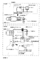
- FIG. 1 is a diagram showing a basic circuit configuration diagram of a wireless power feeding system according to the present invention.
- the wireless power feeding system according to the present invention is composed of a combination of a power feeding device 10 and a power receiving device 2. Electrical energy is supplied from the power supply 10 to the power receiver 2.
- the power receiving device 2 includes a power receiving coil 1, a power receiving side resonance capacitor 3, a rectifier circuit 4, and a load 5 such as a battery.
- the resonance capacitor 3 is composed of a single capacitor or a plurality of capacitors in parallel.
- the power receiver 2 side There are some characteristic points on the power receiver 2 side.
- the power receiver 2 is equipped with a load 5 such as some kind of battery.
- the size, material, and electrical specifications of the power receiving coil 1 provided in the power receiving device 2 and the power feeding coil 11 of the power feeding device 10 are designed according to the power feeding range, the power feeding distance, and the power feeding capacity.
- the power receiving coil 1 of the power receiving device 2 and the power receiving side resonance capacitor 3 have a so-called resonator (LC resonance circuit) configuration, and have specifications having good characteristics at a predetermined resonance frequency.
- the rectifier circuit when the power receiver 2 is a parallel resonant circuit may be half-wave rectifier.
- the allowable deviation width of the resonance frequency is large, it is possible to sufficiently and realistically deal with the problem of the variation in the manufactured electrical performance, that is, the so-called yield. Therefore, it is conceivable to determine the resonance frequency for each model.
- the power supply coil 10 includes a power supply coil 11, a resonance capacitor 14 that constitutes a resonance circuit together with the power supply coil 11, a switch circuit 12 for turning power on and off the power supply coil 11, and a control circuit 17 that operates the switch circuit 12. doing.
- the resonance capacitor 14 is composed of a single capacitor or a plurality of capacitors in parallel.
- a frequency adjustment circuit 15 (for example, a circuit including a PLL circuit) that creates a switch on / off timing is connected to the control circuit 17.
- a current sensor 19 and a voltage sensor 20 are connected to the resonance state sensor 16.
- the power supply unit 10 is provided with a power supply 18 that supplies power to the power supply coil 11 and supplies power required for each circuit.
- the features on the power supply device 10 side are listed.
- the feeding coil 11 and the resonance capacitor 14 form a parallel resonance circuit.
- the control circuit 17 controls the switch circuit 14 by using the timing of the frequency adjustment circuit 15, and controls the timing of the drive state and the resonance state.
- it has a resonance state sensor 16 that detects a resonance state (mainly a frequency shift), and the control circuit 17 controls to stop feeding and adjusts the resonance frequency based on the detection result of the resonance state sensor 16. Control the frequency.
- FIG. 1 shows a basic circuit diagram (close to a block diagram).
- a feeding coil 11 is provided to generate magnetic flux and cause electromagnetic induction.
- At least the electric circuit of the power feeder 10 is provided with a power supply side resonance capacitor 14 and a power supply 18, and creates a resonance relationship with the power receiving coil 1 of the power receiver 2 at a constant frequency.
- the frequency at this time is called a resonance frequency, and generally, a frequency from 100 kHz to 300 kHz, which is said to be a long wave that has little effect on the human body, is used. If this is used as a reference resonance frequency, the reference resonance frequency used in the present invention is not particularly limited.
- the resonance frequency on the feeder side and the resonance frequency on the power receiving side which will be described later, are usually adjusted to the same resonance frequency, but the resonance frequency is shifted based on a predetermined timing time.
- the resonance frequency on the feeder side and the resonance frequency on the power receiving side which will be described later, are usually adjusted to the same resonance frequency, but the resonance frequency is shifted based on a predetermined timing time.
- the resonance frequency slightly deviates depending on the positional relationship and state of the power receiver 2. For example, the situation changes depending on the position and inclination of the power receiving coil of the power receiving device 2. Therefore, if the power receiving coil 1 is within the range where the magnetic flux transmitted from the power feeding coil 11 reaches, energy can be supplied. At this time, the magnetic coupling state between the coil windings is generally referred to as a coupling coefficient (K), which indicates the degree of coupling.
- K the magnetic coupling coefficient
- the present invention also has a feature regarding a method of determining a predetermined coupling coefficient that enhances the feeding efficiency. The entry of the power receiving coil 1 into the magnetic flux affects the feeder side in the form of a deviation in the resonance frequency. If the resonance frequency shifts, the efficiency of energy supply decreases.
- the shifted frequency and phase are detected by the resonance state sensor 16 (for example, a circuit including a phase detection circuit), and the resonance frequency of the feeding coil 11 is adjusted according to the frequency and phase. For example, it can be adjusted by changing the resonance capacitor 14.
- This adjustment is also called tuning, and there are a method of performing it at the time of manufacturing and a method of automatically controlling it by an adjustment circuit at the time of operation, but they are collectively called a tuning adjustment circuit.
- Resonance capacitors are composed of one or more capacitors, but the simplest tuning method is to connect several types of capacitors in parallel in advance so that they do not need to be manufactured at the specified resonance frequency. There is a method of adjusting the resonance frequency by cutting the pattern of the capacitor and disabling it.
- the power receiving side often takes a method of adjusting at the time of manufacturing, but a method of measuring the inductance of the power receiving coil in advance and mounting a capacitor corresponding to it in the unmounted part is also tuned in a broad sense. It can be said to be an adjustment circuit. By connecting capacitors in parallel, it has the effect of reducing internal resistance and further suppressing heat generation.
- the frequency adjustment circuit 15 can adjust the power supply capacity (electric power) by lengthening or shortening the drive state time by, for example, a circuit having a built-in PLL (phase locked loop) circuit. .. In some cases, it is conceivable to change the resonance frequency by having a plurality of feeding coils 11 and switching them.
- the optimum resonance frequency adjustment value by frequency adjustment is a characteristic of the present invention in that the resonance frequency is set to a deviated resonance frequency based on a predetermined timing time described later.
- control circuit 17 that is controlled by a program using a microcontroller (integrated circuit including a processor, a memory, and peripheral circuits) or a programmable logic device (an integrated circuit in which an internal logic circuit can be defined / changed). ..
- the control circuit 17 is connected to the resonance state sensor 16 (phase detection circuit).
- the resonance state sensor 16 senses a frequency shift or a phase shift and transmits the signal to the control circuit 17.
- the resonance state sensor 16 detects an abnormal frequency or phase, transmits the signal to the control circuit 17, and the control circuit 17 acts on the power supply 18. It becomes possible to stop the power supply.
- the wireless power feeding system of the present invention is composed of the basic circuit shown in FIG.
- the position of the resonance capacitor 14 of the feeder 10 is connected in parallel with the feeder coil 11.
- the circuit in which the resonance capacitor 14 is arranged is generally called a parallel resonance circuit.
- a series resonance circuit is formed, and the position of this resonance capacitor is arranged in series with the coil.
- this parallel resonance circuit when SW1 is turned on and a stable resonance state is reached, and then SW1 is turned off, resonance with the power receiver 2 is performed while the energy stored in the power receiving coil 1 and the capacitor 3 is released. The feature is that the feeder 10 continues the state.
- the control circuit 17 is in the drive state by the resonance capacitor and the frequency adjustment circuit (PLL circuit) 15. Achieve a suitable frequency power supply through timing control.
- the resonance state sensor 16 is a sensor that detects a resonance state, and detects a voltage / current transition, a phase detection of a resonance frequency, and the like.
- control circuit 17 controls and adjusts the resonance capacitor
- a special component such as a variable capacitor (a capacitor whose electric capacity can be changed by moving one of the electrodes) that can be finely controlled is ideal. At present, there are few realistic parts, so even if it is used as a fixed frequency without adjustment, it is possible to present a specification value that can sufficiently meet the needs. Also, a method of switching a plurality of coils can be considered. In addition, the resonance frequency is also adjusted by adjusting the drive time.
- a detailed example of the switch circuit 12 of FIG. 1 is composed of an N-channel MOSFET and a Schottky barrier diode. Further, in the detailed example of the rectifier circuit 4 of the power receiver 2, it is composed of a capacitor, a voltage stabilizing circuit 6, and a Schottky barrier diode 7. These are just examples, and have a suitable configuration depending on the product specifications. Further, according to this method, the inductance in the coil does not have to be high, and if possible, if the coil has a low resistance, the requirement is satisfied, and the effect of low loss is high.
- the power feeding coil on the power feeding device side has a size larger than that of the power receiving coil, the power feeding coil can supply power to a plurality of power receiving devices with high efficiency.
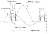
- FIG. 2 shows a drive voltage pulse 21 as a pulse waveform for controlling the switch circuit 14, which is a basic waveform diagram of the feeder 10 of FIG.
- This drive voltage pulse is the waveform at point A in FIG. 1, and is exactly a pulse generated by controlling the switch circuit 14 by the control circuit 17 from the timing of the frequency adjustment circuit 15.
- the switch is turned on when the drive voltage pulse 21 is high. That is, when the switch is turned on, the power of the power supply 18 is supplied to the resonance capacitor 14, so that the drive state is established.
- This drive time 28 (t1) is referred to as a drive pulse width 25.
- the time when the switch is turned off and not driven is the resonance state, that is, the resonance time.
- the resonance time 29 (t2) is referred to as a feeding side resonance period 26 (t2).
- the resonance coil voltage 23 is set to near the zero value (it can be said that the drive voltage pulse is supplied at the timing when the drive voltage pulse is close to the zero value). .. Further, the resonant coil current 22 shows a distorted waveform as a result during the driving time 28. During the drive time 28, the resonance coil voltage 23 is zero and the drive current 24 is flowing. The drive current 24 is a waveform at point B in FIG. The resonance capacitor 14 appears as an AC waveform with the resonance coil current being 90 degrees out of phase, but the drive current 24 is a part of the power energy stored in the resonance capacitor 14. ..
- the present invention shows an advantageous feature.
- the resonance coil voltage 23 is in a state near zero, but at this time, when the switch circuit 14 is switched, if a voltage is applied, a switching loss due to so-called switching occurs. To do. Since it is caused by the overlap of current and voltage, the present invention has the effect of minimizing the switching loss by switching the resonant coil voltage 23 in a state near zero. Further, since the drive current 24 flowing here does not exceed the resonance coil current 22, a high current peak waveform is not generated. As a result, it is possible to suppress switching loss and stress, and since these losses can be said to be heat loss, it also leads to the effect that heat is less likely to be generated.
- the drive pulse is turned on before the resonance coil voltage 23 reaches a zero value. This is because there is a delay in switching, so the drive pulse is turned on before the zero value, that is, near the zero value. Furthermore, the reason why the value is not zero is that the switching circuit has a resistance value, and the voltage is output accordingly. In any case, this explanation shows the essential idea of the method.
- the length of the drive pulse width of the drive voltage pulse 21 and the strength of the drive voltage pulse during the drive time appear as the power energy supplied to the power receiver 1, that is, the power supply capacity. That is, if it is desired to increase the power according to the power to be supplied to the power receiver 1, it is realized by increasing the drive pulse width 25 and increasing the drive voltage pulse 21. If you want to make it smaller, vice versa. However, if the drive pulse width 25 is lengthened, the coupling of the power receiving device 1 with the power receiving coil is strengthened, and if it is strengthened too much, the efficiency is deteriorated. Therefore, it is not necessary to simply lengthen the drive pulse width 25.
- the limit of the design value of the desired power of the power receiver is naturally determined.
- the specifications of the power supply coil 11 and the power reception coil 1 are also closely related, and the specifications of the power supply range and the power supply distance are also related. The specifications of the pulse width will be decided.
- the design value of the feeding coil 11 of the feeding device 10 and the resonance capacitor 14 as a resonator, that is, the resonance frequency can be determined.
- the resonance frequency of the feeder 10 is determined by the period time of the resonance cycle 26 on the feeding side.
- the power receiver 2 it is determined by the cycle time of the power receiving side resonance cycle 27, which is the sum of the drive pulse width 25 and the cycle time of the feeding side resonance cycle 26. From this, in the present invention, it is the matter most showing the feature of the present invention that the resonance frequency of the feeder 10 and the resonance frequency of the power receiver 1 are adjusted with a predetermined deviation.
- FIG. 3 is a basic waveform diagram on the power receiving side of the present invention.
- the drive voltage pulse 31 the drive current 34
- the drive side resonance coil voltage 33 are shown in an overlapping manner.
- the drive current 34 flows, and after a certain delay time 35, the power receiving side diode current 32 flows.
- the power receiving side diode current 32 is a waveform at point C in FIG. This current is the input current to the Schottky barrier diode 7 of the rectifier circuit 4 on the power receiving side.
- the power receiving coil 1 When the steady state of resonance is reached, when the drive current 34 flows through the power feeding coil 10 on the power feeding side, the power receiving coil 1 is electromagnetically induced by electromagnetic induction, and the input current to the power receiving side rectifier circuit, that is, the power receiving side diode current 32 becomes. It peaks during the drive time. Power can be taken out by rectifying this current and connecting it to the load.
- the power receiving coil current 35 simply indicates the period of the resonance frequency on the power receiving side. That is, the power receiving side resonance period 37 is the period obtained by adding the time of the drive voltage pulse 31 to the period of the resonance frequency of the drive side resonance coil voltage 33, that is, 0.9 (t1 + t2) ⁇ t3 ⁇ 1.1 (t1 + t2). It turns out that the conditions are met.
- the switch of the switch circuit 14 when the switch of the switch circuit 14 is turned off, the electric power charged in the resonance capacitor becomes a current and flows into the power feeding coil 11 in the closed circuit system, and is connected to the power receiving coil 1 of the power receiving device 2.
- Form an ideal resonance state At this time as well, magnetic flux is generated by the power feeding coil 11 and causes electromagnetic induction in the power receiving coil 1 of the power receiving device 2.
- the stronger the resonance state also referred to as the steady state
- the waveform of the power receiver 2 shows a relatively clean resonance waveform according to the power receiving side resonance cycle 27 in a state where the resonance coil current and the resonance coil voltage are 90 degrees out of phase. Then, the energy of the current flowing when the feeder 10 has a drive time of 28 changes to a magnetic flux, and when the power receiving coil 1 receives the energy, it appears as a current. When a load is applied by this current, it can be taken out as electric power.
- the resonance frequency of the receiver 2 that is, the duty ratio of about 1/4 or less of the resonance period is set.
- the power feeding capacity (power that can be supplied) is almost maximized when the drive pulse width 25 is about 16% of the duty ratio. For 16% to 25%, power consumption increases but power supply capacity does not increase much. Moreover, even if it is too low, the power supply capacity does not increase.
- the drive pulse width 25 with a duty ratio of about 5% to 16%, it is possible to control the power feeding capacity (power that can be supplied) to be lowered or increased.
- the power receiver can be controlled by the duty ratio according to the adjustment of the amount of light with the light device and the state of charge of the battery (power decreases when fully charged, etc.).
- the drive time is extended too much or the coupling coefficient is high, the balance of the resonance state will be lost, and for example, the resonance coil voltage will rise abnormally, which will cause damage to electronic components.
- the specifications of the drive pulse width, the specifications of the power feeding coil 11 and the power receiving coil 1, the specifications of the power feeding range and the power feeding distance may be determined so as to obtain this coupling coefficient.
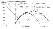
- FIG. 4 is a graph example of the feeding distance and the feeding efficiency.
- FIG. 5 is a graph example of the coupling coefficient and the feeding efficiency. That is, as shown in the data 51 of the general series resonant circuit of FIG. 5, the higher the coupling coefficient, the higher the feeding efficiency. This indicates that the position where the feeding efficiency of the data 41 of the general series resonant circuit of FIG. 4 is high is when the feeding distance is zero. That is, the coupling coefficient increases when the distance between the feeding coil 11 and the power receiving coil 1 is short, and decreases when the distance is long.
- the higher the coupling coefficient the more energy can be sent. Therefore, the closer the distance between the power feeding coil 11 and the power receiving coil 1 is, the higher the energy power feeding efficiency.
- FIG. 6 shows an example of a graph of power supply efficiency, output power, and coupling coefficient. It can be seen that the Duty of the drive pulse can be maintained at a high value in both the power supply efficiency and the output power in the range of 15% to 30%.
- the power feeding coil 11 it is possible to make the power feeding coil 11 larger than the power receiving coil 1 by taking advantage of the high power feeding efficiency where the coupling coefficient is relatively low. Since the coupling coefficient is related to the magnetic flux entering the power receiving coil 1, it suffices if the coupling coefficient is appropriate even if the size of the power receiving coil is difficult to receive the magnetic flux. In this relationship, the feeding distance can be extended by the size of the feeding coil 11. In addition, it is possible to effectively utilize the unused magnetic flux and easily supply power to a plurality of power receivers wirelessly.
- the power receiver 2 side is often provided with a frequency detection circuit and a communication means to the power supply 10 that indicates the state of the power receiver 2. .. It transmits to the feeder 10 by a communication means, and the feeder 10 has a mechanism for appropriately adjusting the resonance frequency. In that case, the power receiver 10 needs a predetermined IC circuit.
- the circuit of the power receiver 2 is configured by a mechanism that simplifies to the utmost limit. With this simplified configuration, it is possible to discharge while charging, so with the charger installed inside the electronic device, it is charged by the wireless power supply system, and at the same time it is discharged to the electronic device to generate electric power. It becomes possible to supply.
- the resonance state sensor 16 composed of the current sensor 21 and the voltage sensor 20 of the power supply device 10. It is possible to detect whether or not the power receiver 1 is in the power supply state by its fluctuation or the like. .. It is possible to determine whether or not the power receiver 1 is present, and take measures such as stopping the power supply 18 by the sleep state, that is, the control circuit 17, or shortening the drive time from the timing of the frequency adjustment circuit 15.
- an overvoltage may be applied to the power supply side at the moment when the power receiver is out of the power supply range. In order to prevent this simply, from the same detection, as overvoltage protection, by setting the drive pulse width to zero, the power supply efficiency can be brought close to zero and the power supply can be temporarily disabled.
- a modulation method called an ASK method for example, amplitude shift keying or amplitude shift keying
- transmission data is transmitted and received by changing the amplitude of a carrier wave corresponding to a bit string of transmission data of a digital signal.
- the power receiver 2 has a unique ID, and when power is supplied, if the power is transmitted to the power supply 1, the unique ID of the power receiving device can be recognized and the power supply capacity (power) suitable for it can be recognized. ) Can be changed. It is also a means that can be effectively used for detecting foreign matter.
- the present invention it is possible to widen the feeding range and increase the feeding capacity (electric power) by having at least a plurality of sets having a feeding coil, a resonance capacitor, and a switch circuit in the feeding device.
- a plurality of main control devices may be provided, or one may be provided. Either way, each pair is controlled to move independently or in cooperation.
- one power supply unit has a main control function for controlling all of them, and appropriately has means for controlling a state of a plurality of power supplies, that is, a power supply stop state, a standby state (sleep state), and a normal state. It is good to feature.
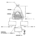
- FIG. 7 is an image diagram having a plurality of units.
- the image is that a plurality of power feeders and power receivers shown in FIG. 1 are made into a unit and are arranged in parallel.
- the power receiving coil unit 71 has an output terminal 72, and a large amount of power can be obtained by collecting the power output from the output terminals of all the power receiving coil units. For example, if one unit is 100 W, 1500 W of electric power can be obtained when all 15 units are completely received.
- Twenty-four feeding coil units 73 are arranged in parallel, six in the feeding range X and four in the feeding range Y.
- the power feeding coil unit 73 is a unit having a power input terminal 74 and at least a control terminal 75 for controlling a switch circuit.
- the input of these powers and the control of the switch circuit may be managed by one main control unit, or each may operate independently.
- the feeding distance at this time becomes the capacity of one feeding distance of the feeding coil unit 73.
- FIG. 8 is an image of having a plurality of units and extending the feeding distance.
- a feeding distance feeding range
- a coupling coefficient showing the high feeding efficiency of the present invention.
- the resonance frequency fluctuates depending on the position of the power receiving coil.
- the feeding coil unit is composed of at least a feeding coil, a resonance capacitor, and a switch circuit, and the specifications are formed by changing the specifications of the feeding coil, the resonance frequency, and the driving time.
- the large power feeding coil unit is designated as A and is connected to the power feeding coil unit circuit A83.
- This coil unit shows the characteristics of the feeding distance A82.
- the feeding distance is also wide by the size of the coil.
- a small power feeding coil unit B it is connected to the power feeding coil unit circuit B84.
- This coil unit exhibits a feeding distance B83, is lower than the feeding distance A, and has a narrow feeding range.
- the power feeding capacity power that can be supplied
- FIG. 8 is a block diagram and is simplified, the control signal line and the resonance state sensor signal line 86 are connected to the control circuit and the like 85 from each power supply coil unit circuit.
- the control circuit sends a control signal while observing the information from the resonance state sensor signal line, and controls each feed coil unit circuit such as turning on / off the feed.
- the distance that can be fed with high efficiency can be expanded in the form of combining the data 42 and 44 of the example of the present invention.
- FIG. 10 is a diagram illustrating the relationship between the phase of the voltage of the capacitor and the phase of the current in the resonance circuit.
- An ideal parallel resonant circuit with no loss transfers energy alternately between the capacitor and coil at the timing of the resonant frequency, and the energy is conserved. However, since there is a loss in reality, the vibration becomes smaller and smaller.
- FIG. 10A shows a state in which the upper electrode of the capacitor is fully charged with a positive charge. Energy is stored only in the capacitor, not in the coil.
- FIG. 10B shows a state in which a capacitor is discharged and a current flows. At this time, the energy stored in the capacitor is transferred to the coil.
- FIG. 10 (c) shows the state where the current is maximum.
- FIG. 10D shows a state in which the current continues to flow and the capacitor is charged in the reverse direction. At this time, the energy stored in the coil is transferred to the capacitor.
- FIG. 10 (e) shows a state in which the reverse charging of the capacitor is completed. The energy of the coil is exhausted and the energy is stored in the capacitor.
- FIG. 10 (f) shows a state in which a capacitor is discharged and a current flows. The direction of the current is opposite to the direction shown in FIG. 10 (b). Comparing the phases, the phase of the current flowing through the coil lags the voltage by 90 °. Also, the phase of the current flowing through the capacitor advances 90 ° ahead of the voltage.
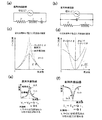
- FIG. 11 is a diagram illustrating the difference between series resonance and parallel resonance.
- FIG. 11A shows the circuit configuration of the series resonant circuit.
- FIG. 11B shows the circuit configuration of the parallel resonant circuit.
- FIG. 11 (c) shows the relationship between the current and the frequency at the time of series resonance. In the series resonance circuit, the impedance is close to zero at the resonance frequency, and the amount of current passing is maximized.
- FIG. 11D shows the relationship between the current and the frequency at the time of parallel resonance. In the parallel resonant circuit, the impedance is close to infinity at the resonant frequency, and the amount of current passing is minimized.
- FIG. 11 (e) shows the relationship with the Q value of the series resonant circuit.
- FIG. 11 (f) shows the relationship with the Q value of the parallel resonant circuit.
- the current of L (coil) and C (capacitor) is Q times the power supply current.
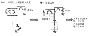
- FIG. 12 is a diagram illustrating a resonance state and a drive state in the parallel resonance circuit.
- FIG. 12A shows a state in which the parallel resonant circuit is stably resonating. Turn the switch on and off to create a state close to alternating current.
- FIG. 12B shows a driving state. When the coil voltage is zero, turn on the switch and connect it to the ground. While the coil current is flowing through the capacitor, the series resonant circuit system operates. That is, the voltage is the minimum and the current flows. Duty ratio control of 5% to 16% is preferred. As a result, parallel resonance and series resonance are repeated in a time-division manner by switching, but at the same time, they also operate as switching, which is necessary for AC oscillation.
- Duty should be switched at 50%, but in the present invention, energy is transferred to the power receiving coil during the drive time, that is, series resonance, so it is more Duty depending on the power to be supplied.
- Duty is too large, the surplus power of AC oscillation ignores switching and restarts oscillation, so switch before that.
- FIG. 13 is a diagram illustrating the relationship between the distance and the coupling coefficient.
- FIG. 13A is a graph showing how much the coupling coefficient changes depending on the distance (distance between the power feeding coil and the power receiving coil) and the deviation (the deviation between the center of the power feeding coil and the center of the power receiving coil).
- FIG. 13B shows a feeding coil used to collect this data.
- a rectangular coil is used in which the vertical direction is three times the diameter of the power receiving coil and the horizontal direction is six times the diameter of the power receiving coil.
- FIG. 13 (c) shows the power receiving coil used to collect this data.
- a coil with 10 turns is used concentrically.
- the coupling coefficient is measured by connecting an impedance analyzer to the power supply side and measuring the impedance in the open and short states of the power receiving side.
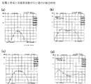
- FIG. 14 shows the coupling characteristics when the resonance frequency is the same on the power feeding side and the power receiving side.
- the core used is a ferrite plate on both the power feeding side and the power receiving side, and the coil is 10 ⁇ H.
- the resonance frequency is the same as 230 KHz.
- FIG. 14A the distance between the power feeding side and the power receiving side is 20 mm.
- FIG. 14B the distance between the power feeding side and the power receiving side is 10 mm.
- the distance between the power feeding side and the power receiving side is 15 mm.
- FIG. 14D the distance between the power feeding side and the power receiving side is 5 mm.
- the single peak characteristic is obtained.
- the bimodal characteristic is obtained.
- the bimodal characteristic appears as shown in this figure.
- the characteristics will improve, but this part has a narrow resonance frequency and is unstable, so it is difficult to use.
- the characteristics are liable to change with respect to the deviation of the resonance frequency caused by the change of the environment such as the feeding distance and the temperature, and it becomes necessary to dynamically adjust the resonance frequency.
- FIG. 15 shows the coupling characteristics when the resonance frequency is different between the power feeding side and the power receiving side.
- the core used is a ferrite plate on both the power feeding side and the power receiving side, and the coil is 10 ⁇ H.
- the resonance frequency is 250 KHz on the power feeding side and 215 KHz on the power receiving side.
- FIG. 15A the distance between the power feeding side and the power receiving side is 20 mm.
- FIG. 15B the distance between the power feeding side and the power receiving side is 10 mm.
- the distance between the power feeding side and the power receiving side is 15 mm.
- the distance between the power feeding side and the power receiving side is 5 mm.
- the single peak characteristic is obtained.
- the distance between the coils is 10 mm and when the distance between the coils is 5 mm, the bimodal characteristic is obtained.
- the resonance frequency is different between the power feeding side and the power receiving side, but as a result, the bimodal characteristic of the coupling characteristic becomes loose, and the resonance frequency that occurs due to changes in the environment such as the feeding distance and temperature Good characteristics can be maintained against deviation. Therefore, in the present invention, once tuning is performed, basically a fixed frequency may be used.
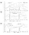
- FIG. 16 is. It is a representative diagram of AC characteristics. In the AC characteristics as well, the bimodal characteristics can be seen depending on the frequency.
- FIG. 16 (a) shows the AC characteristics when the coupling coefficient is 4%
- FIG. 16 (b) shows the coupling coefficient of 10%
- FIG. 16 (c) shows the AC characteristics when the coupling coefficient is 15%.
- This figure is a diagram for finding an appropriate coupling coefficient and the validity of the deviation of the resonance frequency between the power feeding side and the power receiving side.
- two peak points of so-called bimodal characteristics appear in the power receiving side AC characteristics. In the system of the present invention, a high output can be obtained even when the coupling coefficient is around 10%. It is thought that this second peak point has an effect.
- the coupling coefficient of 10% is appropriate and the resonance frequency of the power feeding side and the power receiving side is different from each other as a result.
- the period, that is, the resonance frequency is obtained from the drive time and the resonance time, but even if the resonance frequency is determined by this AC characteristic, almost the same result can be obtained.
- the coupling coefficient 4%
- an appropriate (feeding side) resonance frequency can be designed based on the fixed coupling coefficient.
- the drive time of the series resonant circuit By showing the same function and loosening the characteristics of the two peaks, and conversely, by using the valley of the two peaks, it is said to be robust, and the resonance frequency in the feeding distance, feeding range, and environmental changes. It was possible to make the device resistant to fluctuations in the frequency.
- the wireless power feeding system of the present invention is an epoch-making one that presents a solution to the established theory that wireless power feeding is not suitable for a parallel resonant circuit.
- it is possible to supply power with a low coupling coefficient and high power supply efficiency, which makes it possible to design a power supply distance, a power supply range, and a flexible power receiving coil, and further, it is possible to supply power to a plurality of power sources at the same time.
- it since it is a parallel resonant circuit, it can be configured with a small number of parts such as a switch circuit, so that the loss in power supply can be reduced and heat generation can be suppressed. From these things, it is possible to expand the possibility of wireless power supply that was not possible until now, and it is used in all industries that require charging.
Landscapes
- Engineering & Computer Science (AREA)
- Power Engineering (AREA)
- Computer Networks & Wireless Communication (AREA)
- Current-Collector Devices For Electrically Propelled Vehicles (AREA)
- Charge And Discharge Circuits For Batteries Or The Like (AREA)
- Near-Field Transmission Systems (AREA)
Priority Applications (5)
| Application Number | Priority Date | Filing Date | Title |
|---|---|---|---|
| EP20903230.9A EP4080728A4 (en) | 2019-12-20 | 2020-12-16 | WIRELESS POWER SUPPLY SYSTEM HAVING TUNING ADJUSTMENT CIRCUIT |
| US17/787,227 US12095281B2 (en) | 2019-12-20 | 2020-12-16 | Wireless power feeding system having tuning adjustment circuit |
| KR1020217030995A KR102898613B1 (ko) | 2019-12-20 | 2020-12-16 | 튜닝조정회로를 갖는 무선급전시스템 |
| CN202080097353.1A CN115152125A (zh) | 2019-12-20 | 2020-12-16 | 具有调谐调整电路的无线功率馈送系统 |
| JP2021565621A JP7141156B2 (ja) | 2019-12-20 | 2020-12-16 | チューニング調整回路を有するワイヤレス給電システム |
Applications Claiming Priority (2)
| Application Number | Priority Date | Filing Date | Title |
|---|---|---|---|
| JP2019230720 | 2019-12-20 | ||
| JP2019-230720 | 2019-12-20 |
Publications (1)
| Publication Number | Publication Date |
|---|---|
| WO2021125228A1 true WO2021125228A1 (ja) | 2021-06-24 |
Family
ID=76477572
Family Applications (1)
| Application Number | Title | Priority Date | Filing Date |
|---|---|---|---|
| PCT/JP2020/046981 Ceased WO2021125228A1 (ja) | 2019-12-20 | 2020-12-16 | チューニング調整回路を有するワイヤレス給電システム |
Country Status (6)
| Country | Link |
|---|---|
| US (1) | US12095281B2 (https=) |
| EP (1) | EP4080728A4 (https=) |
| JP (1) | JP7141156B2 (https=) |
| KR (1) | KR102898613B1 (https=) |
| CN (1) | CN115152125A (https=) |
| WO (1) | WO2021125228A1 (https=) |
Cited By (2)
| Publication number | Priority date | Publication date | Assignee | Title |
|---|---|---|---|---|
| WO2023128436A1 (ko) * | 2021-12-30 | 2023-07-06 | 삼성전자 주식회사 | 무선 전력 송신 장치 및 이를 포함하는 전자 장치 |
| WO2026053779A1 (ja) * | 2024-09-06 | 2026-03-12 | 横浜ゴム株式会社 | 電源ユニット、センサモジュール及びそれを備えたタイヤ並びに無線給電システム |
Families Citing this family (3)
| Publication number | Priority date | Publication date | Assignee | Title |
|---|---|---|---|---|
| US12212152B2 (en) * | 2019-02-21 | 2025-01-28 | Raisontech Inc. | Wireless power feeding system, and power receiver having circular, spherical, or polyhedral shape |
| US20230004208A1 (en) * | 2019-12-06 | 2023-01-05 | Hewlett-Packard Development Company, L.P. | Induced current-based power supply control |
| JP7626512B1 (ja) * | 2023-04-20 | 2025-02-04 | 株式会社レゾンテック | チューニング調整回路を有するワイヤレス給電システム |
Citations (7)
| Publication number | Priority date | Publication date | Assignee | Title |
|---|---|---|---|---|
| WO2013128815A1 (ja) * | 2012-02-29 | 2013-09-06 | パナソニック株式会社 | 充電装置 |
| JP2013243882A (ja) * | 2012-05-22 | 2013-12-05 | Toyota Motor Corp | 送電装置、受電装置、車両、および非接触給電システム |
| WO2014068992A1 (ja) * | 2012-11-02 | 2014-05-08 | パナソニック株式会社 | 無線電力伝送システム |
| JP2015053751A (ja) * | 2013-09-05 | 2015-03-19 | Tdk株式会社 | 非接触電力伝送装置 |
| KR20170028998A (ko) | 2014-07-10 | 2017-03-14 | 코닝 인코포레이티드 | 냉간 성형된 유리 아플리케 |
| KR20170028770A (ko) | 2015-09-04 | 2017-03-14 | 이용을 | 탄성체로 이루어진 체결구를 갖는 조립식 블록 |
| JP2017528106A (ja) * | 2014-09-16 | 2017-09-21 | コーニンクレッカ フィリップス エヌ ヴェKoninklijke Philips N.V. | 無線誘導電力伝送 |
Family Cites Families (14)
| Publication number | Priority date | Publication date | Assignee | Title |
|---|---|---|---|---|
| JP5736991B2 (ja) * | 2010-07-22 | 2015-06-17 | Tdk株式会社 | ワイヤレス給電装置およびワイヤレス電力伝送システム |
| CN103329398B (zh) * | 2011-01-26 | 2015-07-01 | 株式会社村田制作所 | 电力输送系统 |
| US9412513B2 (en) * | 2012-03-30 | 2016-08-09 | Tdk Corporation | Wireless power transmission system |
| JP2014030288A (ja) * | 2012-07-31 | 2014-02-13 | Sony Corp | 給電装置および給電システム |
| CN106961164A (zh) | 2012-10-11 | 2017-07-18 | 株式会社村田制作所 | 无线供电装置 |
| JP2014176122A (ja) | 2013-03-06 | 2014-09-22 | Osaka City Univ | 磁気共振型ワイヤレス給電システム |
| US9831684B2 (en) * | 2014-08-08 | 2017-11-28 | Texas Instruments Incorporated | Adaptive rectifier and method of operation |
| JP2016067135A (ja) * | 2014-09-25 | 2016-04-28 | 東芝テック株式会社 | 非接触給電装置 |
| KR20170100649A (ko) * | 2014-12-29 | 2017-09-04 | 에너저스 코포레이션 | 무선 전력 전송을 위한 시스템 및 방법 |
| JP6555517B2 (ja) | 2015-07-16 | 2019-08-07 | 清水建設株式会社 | ワイヤレス給電システム |
| JP2017163647A (ja) | 2016-03-08 | 2017-09-14 | 達也 土井 | 電磁界共振ワイヤレス給電方法及び給電システム |
| WO2018037758A1 (ja) * | 2016-08-23 | 2018-03-01 | 株式会社村田製作所 | 受電装置および送電装置 |
| CN110556925B (zh) | 2018-05-31 | 2022-12-27 | 华为技术有限公司 | 一种无线充电器和控制方法 |
| US12068615B2 (en) * | 2020-11-09 | 2024-08-20 | Aira, Inc. | Free-boost class-E amplifier |
-
2020
- 2020-12-16 KR KR1020217030995A patent/KR102898613B1/ko active Active
- 2020-12-16 JP JP2021565621A patent/JP7141156B2/ja active Active
- 2020-12-16 WO PCT/JP2020/046981 patent/WO2021125228A1/ja not_active Ceased
- 2020-12-16 EP EP20903230.9A patent/EP4080728A4/en not_active Withdrawn
- 2020-12-16 US US17/787,227 patent/US12095281B2/en active Active
- 2020-12-16 CN CN202080097353.1A patent/CN115152125A/zh active Pending
Patent Citations (7)
| Publication number | Priority date | Publication date | Assignee | Title |
|---|---|---|---|---|
| WO2013128815A1 (ja) * | 2012-02-29 | 2013-09-06 | パナソニック株式会社 | 充電装置 |
| JP2013243882A (ja) * | 2012-05-22 | 2013-12-05 | Toyota Motor Corp | 送電装置、受電装置、車両、および非接触給電システム |
| WO2014068992A1 (ja) * | 2012-11-02 | 2014-05-08 | パナソニック株式会社 | 無線電力伝送システム |
| JP2015053751A (ja) * | 2013-09-05 | 2015-03-19 | Tdk株式会社 | 非接触電力伝送装置 |
| KR20170028998A (ko) | 2014-07-10 | 2017-03-14 | 코닝 인코포레이티드 | 냉간 성형된 유리 아플리케 |
| JP2017528106A (ja) * | 2014-09-16 | 2017-09-21 | コーニンクレッカ フィリップス エヌ ヴェKoninklijke Philips N.V. | 無線誘導電力伝送 |
| KR20170028770A (ko) | 2015-09-04 | 2017-03-14 | 이용을 | 탄성체로 이루어진 체결구를 갖는 조립식 블록 |
Non-Patent Citations (1)
| Title |
|---|
| See also references of EP4080728A4 |
Cited By (3)
| Publication number | Priority date | Publication date | Assignee | Title |
|---|---|---|---|---|
| WO2023128436A1 (ko) * | 2021-12-30 | 2023-07-06 | 삼성전자 주식회사 | 무선 전력 송신 장치 및 이를 포함하는 전자 장치 |
| US12562597B2 (en) | 2021-12-30 | 2026-02-24 | Samsung Electronics Co., Ltd. | Wireless power transmission device, and electronic device comprising same |
| WO2026053779A1 (ja) * | 2024-09-06 | 2026-03-12 | 横浜ゴム株式会社 | 電源ユニット、センサモジュール及びそれを備えたタイヤ並びに無線給電システム |
Also Published As
| Publication number | Publication date |
|---|---|
| KR102898613B1 (ko) | 2025-12-10 |
| US20230016332A1 (en) | 2023-01-19 |
| EP4080728A1 (en) | 2022-10-26 |
| KR20220118296A (ko) | 2022-08-25 |
| JP7141156B2 (ja) | 2022-09-22 |
| US12095281B2 (en) | 2024-09-17 |
| JPWO2021125228A1 (https=) | 2021-06-24 |
| EP4080728A4 (en) | 2024-03-13 |
| CN115152125A (zh) | 2022-10-04 |
Similar Documents
| Publication | Publication Date | Title |
|---|---|---|
| JP7141156B2 (ja) | チューニング調整回路を有するワイヤレス給電システム | |
| JP3692541B2 (ja) | 電力伝送装置及び電力伝送方法 | |
| US9478992B2 (en) | Power transmission system | |
| CN1768467B (zh) | 自适应感应电源及其操作方法 | |
| JPWO1998034319A1 (ja) | 電力伝送装置及び電力伝送方法 | |
| JP5801154B2 (ja) | 非接触電力伝送装置及び非接触電力伝送方法 | |
| EP2912751B1 (en) | High power rf field effect transistor switching using dc biases | |
| EP2754225B1 (en) | Wireless power apparatus and operation method thereof | |
| US20170256956A1 (en) | Multi-impedance rectification for wireless power transfer | |
| KR20140109402A (ko) | 무선 전력 수신기 시스템 | |
| JP7003708B2 (ja) | 非接触給電装置 | |
| US9960608B2 (en) | High frequency multi-level rectification | |
| JP2010136464A (ja) | 電力伝送装置および電力伝送方法 | |
| CN101322142A (zh) | 用于应答器的电路设置和用于操作电路设置的方法 | |
| CN112448484B (zh) | 非接触供电装置 | |
| JPWO2021125228A5 (https=) | ||
| JP2019176565A (ja) | 非接触給電装置 | |
| KR20150021285A (ko) | 무선전력 수신장치 | |
| JP7070347B2 (ja) | 非接触給電装置 | |
| JP5571177B2 (ja) | 誘導エネルギー伝送のための回路構成及び方法 | |
| CN113300443A (zh) | 一种浮频调谐无线充电装置 | |
| Rohith et al. | Wireless transmission of solar power using inductive resonant principle | |
| JP2023088141A (ja) | 非接触給電装置 | |
| JP7626512B1 (ja) | チューニング調整回路を有するワイヤレス給電システム | |
| JP7800549B2 (ja) | 近距離無線通信装置 |
Legal Events
| Date | Code | Title | Description |
|---|---|---|---|
| 121 | Ep: the epo has been informed by wipo that ep was designated in this application |
Ref document number: 20903230 Country of ref document: EP Kind code of ref document: A1 |
|
| ENP | Entry into the national phase |
Ref document number: 2021565621 Country of ref document: JP Kind code of ref document: A |
|
| NENP | Non-entry into the national phase |
Ref country code: DE |
|
| ENP | Entry into the national phase |
Ref document number: 2020903230 Country of ref document: EP Effective date: 20220720 |
|
| WWW | Wipo information: withdrawn in national office |
Ref document number: 2020903230 Country of ref document: EP |