WO2021125138A1 - 半導体記憶装置 - Google Patents
半導体記憶装置 Download PDFInfo
- Publication number
- WO2021125138A1 WO2021125138A1 PCT/JP2020/046574 JP2020046574W WO2021125138A1 WO 2021125138 A1 WO2021125138 A1 WO 2021125138A1 JP 2020046574 W JP2020046574 W JP 2020046574W WO 2021125138 A1 WO2021125138 A1 WO 2021125138A1
- Authority
- WO
- WIPO (PCT)
- Prior art keywords
- nanosheet
- storage device
- power supply
- memory cell
- semiconductor storage
- Prior art date
- Legal status (The legal status is an assumption and is not a legal conclusion. Google has not performed a legal analysis and makes no representation as to the accuracy of the status listed.)
- Ceased
Links
Images









Classifications
-
- H—ELECTRICITY
- H10—SEMICONDUCTOR DEVICES; ELECTRIC SOLID-STATE DEVICES NOT OTHERWISE PROVIDED FOR
- H10B—ELECTRONIC MEMORY DEVICES
- H10B20/00—Read-only memory [ROM] devices
- H10B20/27—ROM only
- H10B20/30—ROM only having the source region and the drain region on the same level, e.g. lateral transistors
- H10B20/34—Source electrode or drain electrode programmed
-
- G—PHYSICS
- G11—INFORMATION STORAGE
- G11C—STATIC STORES
- G11C17/00—Read-only memories programmable only once; Semi-permanent stores, e.g. manually-replaceable information cards
- G11C17/08—Read-only memories programmable only once; Semi-permanent stores, e.g. manually-replaceable information cards using semiconductor devices, e.g. bipolar elements
- G11C17/10—Read-only memories programmable only once; Semi-permanent stores, e.g. manually-replaceable information cards using semiconductor devices, e.g. bipolar elements in which contents are determined during manufacturing by a predetermined arrangement of coupling elements, e.g. mask-programmable ROM
- G11C17/12—Read-only memories programmable only once; Semi-permanent stores, e.g. manually-replaceable information cards using semiconductor devices, e.g. bipolar elements in which contents are determined during manufacturing by a predetermined arrangement of coupling elements, e.g. mask-programmable ROM using field-effect devices
-
- H—ELECTRICITY
- H10—SEMICONDUCTOR DEVICES; ELECTRIC SOLID-STATE DEVICES NOT OTHERWISE PROVIDED FOR
- H10D—INORGANIC ELECTRIC SEMICONDUCTOR DEVICES
- H10D30/00—Field-effect transistors [FET]
- H10D30/60—Insulated-gate field-effect transistors [IGFET]
- H10D30/67—Thin-film transistors [TFT]
- H10D30/6729—Thin-film transistors [TFT] characterised by the electrodes
- H10D30/673—Thin-film transistors [TFT] characterised by the electrodes characterised by the shapes, relative sizes or dispositions of the gate electrodes
- H10D30/6735—Thin-film transistors [TFT] characterised by the electrodes characterised by the shapes, relative sizes or dispositions of the gate electrodes having gates fully surrounding the channels, e.g. gate-all-around
-
- H—ELECTRICITY
- H10—SEMICONDUCTOR DEVICES; ELECTRIC SOLID-STATE DEVICES NOT OTHERWISE PROVIDED FOR
- H10D—INORGANIC ELECTRIC SEMICONDUCTOR DEVICES
- H10D30/00—Field-effect transistors [FET]
- H10D30/60—Insulated-gate field-effect transistors [IGFET]
- H10D30/67—Thin-film transistors [TFT]
- H10D30/6757—Thin-film transistors [TFT] characterised by the structure of the channel, e.g. transverse or longitudinal shape or doping profile
-
- H—ELECTRICITY
- H10—SEMICONDUCTOR DEVICES; ELECTRIC SOLID-STATE DEVICES NOT OTHERWISE PROVIDED FOR
- H10D—INORGANIC ELECTRIC SEMICONDUCTOR DEVICES
- H10D62/00—Semiconductor bodies, or regions thereof, of devices having potential barriers
- H10D62/10—Shapes, relative sizes or dispositions of the regions of the semiconductor bodies; Shapes of the semiconductor bodies
- H10D62/117—Shapes of semiconductor bodies
- H10D62/118—Nanostructure semiconductor bodies
-
- B—PERFORMING OPERATIONS; TRANSPORTING
- B82—NANOTECHNOLOGY
- B82Y—SPECIFIC USES OR APPLICATIONS OF NANOSTRUCTURES; MEASUREMENT OR ANALYSIS OF NANOSTRUCTURES; MANUFACTURE OR TREATMENT OF NANOSTRUCTURES
- B82Y10/00—Nanotechnology for information processing, storage or transmission, e.g. quantum computing or single electron logic
-
- H—ELECTRICITY
- H10—SEMICONDUCTOR DEVICES; ELECTRIC SOLID-STATE DEVICES NOT OTHERWISE PROVIDED FOR
- H10D—INORGANIC ELECTRIC SEMICONDUCTOR DEVICES
- H10D30/00—Field-effect transistors [FET]
- H10D30/40—FETs having zero-dimensional [0D], one-dimensional [1D] or two-dimensional [2D] charge carrier gas channels
- H10D30/43—FETs having zero-dimensional [0D], one-dimensional [1D] or two-dimensional [2D] charge carrier gas channels having one-dimensional [1D] charge carrier gas channels, e.g. quantum wire FETs or transistors having 1D quantum-confined channels
-
- H—ELECTRICITY
- H10—SEMICONDUCTOR DEVICES; ELECTRIC SOLID-STATE DEVICES NOT OTHERWISE PROVIDED FOR
- H10D—INORGANIC ELECTRIC SEMICONDUCTOR DEVICES
- H10D62/00—Semiconductor bodies, or regions thereof, of devices having potential barriers
- H10D62/10—Shapes, relative sizes or dispositions of the regions of the semiconductor bodies; Shapes of the semiconductor bodies
- H10D62/117—Shapes of semiconductor bodies
- H10D62/118—Nanostructure semiconductor bodies
- H10D62/119—Nanowire, nanosheet or nanotube semiconductor bodies
- H10D62/121—Nanowire, nanosheet or nanotube semiconductor bodies oriented parallel to substrates
Definitions
- the present disclosure relates to a semiconductor storage device provided with a nanosheet (nanowire) FET (Field Effect Transistor), and more particularly to a layout structure of a mask ROM (Read Only Memory) using the nanosheet FET.
- a nanosheet nanowire
- FET Field Effect Transistor
- the mask ROM includes memory cells arranged in an array, and each memory cell is programmed and manufactured so as to have a fixed data state.
- the transistor constituting the memory cell is provided between the bit line and the VSS, and the word line is connected to the gate.
- Bit data "1" / "0" is stored depending on whether the source or drain is connected to the bit line or VSS.
- the presence or absence of connection is realized by, for example, the presence or absence of contacts or vias.
- the transistor which is a basic component of the LSI, has realized an improvement in the degree of integration, a reduction in the operating voltage, and an improvement in the operating speed by reducing (scaling) the gate length.
- off-current due to excessive scaling and a significant increase in power consumption due to the off-current have become problems.
- three-dimensional structure transistors in which the transistor structure is changed from the conventional two-dimensional type to the three-dimensional type are being actively studied. As one of them, nanosheet (nanowire) FETs are attracting attention.
- Non-Patent Documents 1 and 2 disclose a layout of a SRAM memory cell using a nanosheet FET having a fork-shaped gate electrode.
- a nanosheet FET having a fork-shaped gate electrode is referred to as a forksheet FET, following the description in Non-Patent Document 1.
- An object of the present disclosure is to provide a layout structure of a mask ROM using a nanosheet FET or a fork sheet FET.
- the semiconductor storage device including the first and second ROM (Read Only Memory) memory cells adjacent to each other in the first direction has a word line extending in the first direction and is perpendicular to the first direction.
- the first ROM memory cell includes the first and second bit lines extending in the second direction and the first and second ground power supply wirings extending in the second direction, and the first ROM memory cell includes the first bit line and the first.
- the second ROM memory cell includes a first nanosheet FET (Field Effect Transistor) provided between the ground power supply wiring and having a first nanosheet as a channel region, and the second ROM memory cell is the second bit line and the second ground power supply.
- a second nanosheet FET which is provided between the wiring and has a second nanosheet as a channel region, is provided, and the word line is the first direction of the first nanosheet and the first and second directions.
- the first ROM memory cell includes a first gate wiring that surrounds the outer circumference in a vertical third direction and a second gate wiring that surrounds the outer circumference in the first direction and the third direction of the second nanosheet.
- the first data is stored by the connection relationship between the node of the first nanosheet FET, the first bit line, and the first ground power supply wiring, and the second ROM memory cell is the node of the second nanosheet FET.
- the second data is stored by the connection relationship between the second bit wire and the second ground power supply wiring, and the first and second nanosheets face each other in the first direction and are opposed to each other.
- the surface on the side of the second nanosheet in the first direction is exposed from the first gate wiring, and the second nanosheet is on the side of the first nanosheet in the first direction. The surface is exposed from the second gate wiring.
- the semiconductor storage device includes first and second ROM memory cells that are adjacent in the first direction.
- the first ROM memory cell is provided between the first bit line and the first ground power supply wiring, and includes a first nanosheet FET having a first nanosheet as a channel region.
- the second ROM memory cell is provided between the second bit line and the second ground power supply wiring, and includes a second nanosheet FET having a second nanosheet as a channel region.
- the first and second nanosheets face each other in the first direction, and the surface of the first nanosheet on the side of the second nanosheet in the first direction is exposed from the first gate wiring. In the two nanosheets, the surface on the side of the first nanosheet in the first direction is exposed from the second gate wiring.
- the distance between the first nanosheet and the second nanosheet can be reduced, so that the area of the semiconductor storage device can be reduced.
- the semiconductor storage device including the ROM (Read Only Memory) memory cell comprises a word line extending in the first direction and a bit line extending in the second direction perpendicular to the first direction.
- the ROM memory cell includes the ground power supply wiring extending in the second direction, the ROM memory cell is provided between the bit wire and the ground power supply wiring, and has a first nanosheet FET as a channel region and a first nanosheet FET.
- the drains are connected to each other, the sources are connected to each other, and the word line is the first direction of the first nanosheet and the third direction perpendicular to the first and second directions.
- the ROM memory cell includes the first gate wiring surrounding the outer periphery of the second nanosheet and the second gate wiring surrounding the outer periphery in the first direction and the third direction of the second nanosheet, and the ROM memory cell is the first and second nanosheet FETs. Data is stored by the connection relationship between the node, the bit wire, and the ground power supply wiring, and the first and second nanosheets face each other in the first direction, and the first nanosheet is opposed to each other. In the nanosheet, the surface on the side of the second nanosheet in the first direction is exposed from the first gate wiring, and in the second nanosheet, the surface on the side of the first nanosheet in the first direction is exposed. It is exposed from the second gate wiring.
- the semiconductor storage device includes a ROM memory cell.
- the ROM memory cell is provided between the bit wire and the ground power supply wiring, and is provided between the first nanosheet FET having the first nanosheet as a channel area and the bit wire and the ground power supply wiring, and is a channel. It includes a second nanosheet FET having a second nanosheet as a region.
- the first and second nanosheet FETs are adjacent in the first direction.
- the first and second nanosheets face each other in the first direction, and the surface of the first nanosheet on the side of the second nanosheet in the first direction is exposed from the first gate wiring. In the two nanosheets, the surface on the side of the first nanosheet in the first direction is exposed from the second gate wiring.
- the distance between the first nanosheet and the second nanosheet can be reduced, so that the size of the ROM memory cell in the first direction can be reduced, and the area of the semiconductor storage device can be reduced. ..
- the semiconductor storage device including the first and second ROM (Read Only Memory) memory cells adjacent to each other in the first direction has a word line extending in the first direction and is perpendicular to the first direction.
- the first ROM memory cell includes the first and second bit wires extending in the second direction forming the above, and a plurality of ground power supply wirings extending in the second direction including the first and second ground power supply wirings.
- the second ROM memory cell includes a first nanosheet FET provided between the first bit line and the first ground power supply wiring and having a first nanosheet as a channel region, and the second ROM memory cell is the second bit line and the second ground.
- a second nanosheet FET provided between the power supply wiring and having a second nanosheet as a channel region is provided, and the word line is perpendicular to the first direction and the first and second directions of the first nanosheet.
- the first ROM memory cell includes the first gate wiring that surrounds the outer periphery in the third direction and the second gate wiring that surrounds the outer periphery in the first direction and the third direction of the second nanosheet.
- the first data is stored by the connection relationship between the node of the 1 nanosheet FET and the first bit line and the first ground power supply wiring, and the second ROM memory cell is the node of the second nanosheet FET and the said.
- the second data is stored by the connection relationship between the second bit line and the second ground power supply wiring, and the first bit line and the first bit line are adjacent to the first side in the first direction.
- the distance from the ground power supply wiring is equal to the distance between the second bit wire and the ground power supply wiring adjacent to the first side of the second bit wire in the first direction.
- the distance between the first bit wire and the ground power supply wiring adjacent to the second side opposite to the first side in the first direction is the distance between the second bit wire and the second bit wire in the first direction. It is equal to the distance from the ground power supply wiring adjacent to the second side.
- the semiconductor storage device includes first and second ROM memory cells that are adjacent in the first direction.
- the first ROM memory cell is provided between the first bit line and the first ground power supply wiring, and includes a first nanosheet FET having a first nanosheet as a channel region.
- the second ROM memory cell is provided between the second bit line and the second ground power supply wiring, and includes a second nanosheet FET having a second nanosheet as a channel region.
- the distance between the first bit wire and the grounded power supply wiring on both sides thereof is equal to the distance between the second bit wire and the grounded power supply wiring on both sides thereof.
- a layout structure having a small area can be realized for a semiconductor storage device using a nanosheet FET or a fork sheet FET.
- (A) to (c) are cross-sectional views of the layout structure of FIG.
- (A) to (c) are cross-sectional views of the layout structure of FIG.
- (A) to (c) are cross-sectional views of the layout structure of FIG.
- the semiconductor storage device is provided with a nanosheet FET (Field Effect Transistor).
- the nanosheet FET is an FET using a thin sheet (nanosheet) through which an electric current flows.
- Nanosheets are made of, for example, silicon.
- a part of the nanosheet FET is a fork sheet FET having a fork-shaped gate electrode.
- a semiconductor layer portion formed at both ends of the nanosheet and forming a terminal serving as a source or drain of the nanosheet FET is referred to as a “pad”.
- FIG. 19 is a diagram showing a basic structure of a fork sheet FET, (a) is a plan view, and (b) is a cross-sectional view taken along the line YY'of (a).
- two transistors TR1 and TR2 are arranged side by side with an interval S in the Y direction.
- the gate wiring 531 that serves as the gate of the transistor TR1 and the gate wiring 532 that serves as the gate of the transistor TR2 both extend in the Y direction and are arranged at the same position in the X direction.
- the channel portion 521 which is the channel region of the transistor TR1 and the channel portion 526 which is the channel region of the transistor TR2 are composed of nanosheets.
- each of the channel portions 521 and 526 is composed of nanosheets having a three-sheet structure that overlaps in a plan view.
- Pads 522a and 522b serving as a source region or a drain region of the transistor TR1 are formed on both sides of the channel portion 521 in the X direction.
- Pads 527a and 527b serving as a source region or a drain region of the transistor TR2 are formed on both sides of the channel portion 526 in the X direction.
- the pads 522a and 522b are formed by epitaxial growth from the nanosheets constituting the channel portion 521.
- the pads 527a and 527b are formed by epitaxial growth from the nanosheets constituting the channel portion 526.
- the gate wiring 531 surrounds the outer circumference of the channel portion 521 made of nanosheets in the Y direction and the Z direction via a gate insulating film (not shown). However, in the nanosheet constituting the channel portion 521, the surface on the side of the transistor TR2 in the Y direction is not covered by the gate wiring 531 and is exposed from the gate wiring 531. That is, in the cross-sectional view of FIG. 19B, the gate wiring 531 does not cover the right side of the drawing of the nanosheet constituting the channel portion 521, but covers the upper side, the left side, and the lower side of the drawing. The gate wiring 531 overlaps the nanosheet constituting the channel portion 521 on the opposite side of the transistor TR2 in the Y direction by the length OL.
- the gate wiring 532 surrounds the outer circumference of the channel portion 526 made of nanosheets in the Y and Z directions via a gate insulating film (not shown). However, in the nanosheet constituting the channel portion 526, the surface on the side of the transistor TR1 in the Y direction is not covered by the gate wiring 532 and is exposed from the gate wiring 532. That is, in the cross-sectional view of FIG. 19B, the gate wiring 532 does not cover the left side of the drawing of the nanosheet constituting the channel portion 526, but covers the upper side, the right side, and the lower side of the drawing. The gate wiring 532 overlaps the nanosheet constituting the channel portion 526 on the opposite side of the transistor TR1 in the Y direction by the length OL.
- the effective gate width Weff 2 ⁇ W + H Will be. Since the channel portions 521 and 526 of the transistors TR1 and TR2 are composed of three nanosheets, the gate effective width of the transistors TR1 and TR2 is determined. 3x (2xW + H) Will be.
- the gate wiring 531 does not overlap the nanosheet constituting the channel portion 521 on the side of the transistor TR2 in the Y direction. Further, the gate wiring 532 does not overlap with the nanosheet constituting the channel portion 526 on the side of the transistor TR1 in the Y direction. As a result, the transistors TR1 and TR2 can be brought closer to each other, and the area can be reduced.
- the number of nanosheets constituting the channel portion of the transistor is not limited to three. That is, the nanosheet may have a single sheet structure, or may have a plurality of overlapping sheet structures in a plan view. Further, in FIG. 19B, the cross-sectional shape of the nanosheet is shown as a rectangle, but the cross-sectional shape of the nanosheet is not limited to this, and the cross-sectional shape of the nanosheet may be, for example, a square, a circle, an ellipse, or the like. ..
- the fork sheet FET and the nanosheet FET in which the gate wiring surrounds the entire circumference of the nanosheet may be mixed in the semiconductor storage device.
- VDD and VVSS indicate the power supply voltage or the power supply itself.
- expressions such as “same wiring width” that mean that the widths and the like are the same include a range of manufacturing variation.
- the source region and the drain region of the transistor are appropriately referred to as "nodes" of the transistor. That is, one node of the transistor refers to the source or drain of the transistor, and both nodes of the transistor refer to the source and drain of the transistor.
- FIG. 1 is a circuit diagram showing a configuration of a contact-type mask ROM as an example of a semiconductor storage device.
- the contact-type mask ROM corresponds to "0" and "1" of the stored data depending on whether the drain of the memory cell transistor is connected to the bit line via the contact or not.
- the mask ROM includes a memory cell array 3, a column decoder 2, and a sense amplifier 18.
- the gates of the memory cells Mij are commonly connected to the word line WLi in the row direction, and their sources are connected to the ground potential VSS.
- the drain of the memory cell Mij is connected to the bit line BLj when the stored data is set to “0”, and is not connected to the bit line BLj when the stored data is set to “1”.
- the column decoder 2 is composed of an N-type MOS transistor Cj.
- the drains are all connected in common, the gate is connected to the column selection signal line CLj, and the source is connected to the bit line BLj.
- the sense amplifier 18 includes a P-type MOS transistor 5 for precharging, an inverter 8 for determining the output data of the memory cell Mij, and an inverter 9 for buffering the output signal of the inverter 8.
- a precharge signal NPR is input to the gate of the P-type MOS transistor 5, a power supply voltage VDD is supplied to the source, and the drain is connected to the common drain of the N-type MOS transistor Cj.
- the inverter 8 receives the signal SIN of the common drain of the N-type MOS transistor Cj and determines the output data of the memory cell Mij.
- the inverter 9 receives the output signal SOUT of the inverter 8 and outputs the stored data of the memory cell Mij.
- the operation of the mask ROM of FIG. 1 will be described by taking the case of reading the data of the memory cell M00 as an example.
- the precharge signal NPR is changed from high level to low level, and the precharge P-type MOS transistor 5 is turned on.
- the current capacity of the memory cell M00 is larger than that of the precharge P-type MOS transistor 5, so that the input signal SIN of the inverter 8 is the switching of the inverter 8.
- the voltage will be lower than the level. Therefore, the output signal SOUT of the inverter 8 holds the high level, and the output signal OUT of the inverter 9 holds the low level.
- the bit line BL0 is charged by the precharging P-type MOS transistor 5, and the input signal SIN of the inverter 8 is higher than the switching level of the inverter 8. It becomes a voltage. Therefore, the output signal SOUT of the inverter 8 becomes a low level, and the output signal OUT of the inverter 9 becomes a high level.
- the mask ROM of the present disclosure is set as a method of storing the value of each memory cell by connecting / disconnecting between the memory cell and the bit line and connecting / disconnecting between the memory cell and VSS. There are cases where it is done.
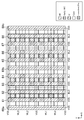
- FIG. 2 and 3 are views showing an example of the layout structure of the mask ROM according to the first embodiment
- FIG. 2 is a plan view of the memory cell array
- FIGS. It is sectional drawing in the horizontal direction in a plan view.
- 3 (a) is a cross section of line X1-X1'
- FIG. 3 (b) is a cross section of line X2-X2'
- FIG. 3 (c) is a cross section of line X3-X3'.
- the horizontal direction of the drawing is the X direction (corresponding to the first direction)
- the vertical direction of the drawing is the Y direction (corresponding to the second direction)
- the direction perpendicular to the substrate surface It is in the Z direction (corresponding to the depth direction).
- the X direction is the direction in which the gate wiring and the word line extend
- the Y direction is the channel direction, which is the direction in which the bit line extends.
- the letter "D" is attached to the contact that determines the storage value of the memory cell.
- FIG. 2 corresponds to the layout for (4 ⁇ 4) bits.
- the broken line indicates the frame of the memory cell for one bit. That is, FIG. 2 shows a configuration in which four memory cells are arranged in the X direction and four in the Y direction. In the Y direction, the memory cells are arranged so as to be inverted in the Y direction every other row. For example, the two memory cells from the left in the bottom row of the drawing correspond to the memory cells M00 and M01 in the circuit diagram of FIG. 1, respectively.
- the structure of the memory cells will be described by taking the memory cells M00 and M01 as an example.
- the M1 wiring layer is formed with wirings 61 to 68 extending in the Y direction.
- the M1 wirings 62, 64, 66, and 68 correspond to the bit lines BL0, BL1, BL2, and BL3, respectively.
- the M1 wirings 61, 63, 65, 67 supply VSS.
- the memory cells M00 and M01 have nanosheets 11 and 12 composed of three sheets, respectively, as channel portions. That is, the memory cells M00 and M01 include nanosheet FETs.
- pads 21a and 22a made of a semiconductor layer having an integral structure connected to three sheets are formed on the lower side of the drawings of the nanosheets 11 and 12, respectively.
- Pads 21b and 22b made of a semiconductor layer having an integral structure connected to three sheets are formed on the upper side of the drawings of the nanosheets 11 and 12, respectively.
- the pads 21a and 21b serve as nodes of the memory cell M00.
- the pads 22a and 22b serve as nodes of the memory cell M01.
- Gate wirings 31 and 32 extending in the X direction are formed.
- the gate wiring 31 surrounds the outer periphery of the nanosheet 11 of the memory cell M00 in the X and Z directions via a gate insulating film (not shown).
- the gate wiring 31 serves as a gate for the memory cell M00.
- the gate wiring 32 surrounds the outer periphery of the nanosheet 12 of the memory cell M01 in the X and Z directions via a gate insulating film (not shown).
- the gate wiring 32 serves as a gate for the memory cell M01.
- the gate wirings 31 and 32 are connected to other gate wirings arranged in a row in the X direction to form the word line WL0. That is, each of the word lines WL0 to WL3 includes gate wiring arranged in a row in the X direction.
- Local wirings 41, 42, 43, 44 extending in the X direction are formed.
- the local wiring 41 is connected to the pad 21a, and the local wiring 42 is connected to the pad 21b.
- the local wiring 43 is connected to the pad 22a, and the local wiring 44 is connected to the pad 22b.
- the local wiring 42 is connected to the M1 wiring 62 via the contact 51.
- the local wiring 44 is connected to the M1 wiring 64 via the contact 52.
- the contacts 71 and 72 determine the stored value of the memory cell depending on the presence or absence of the contacts 71 and 72.
- the contact 71 connects the local wiring 41 and the M1 wiring 61 that supplies VSS.
- the contact 72 when formed, connects the local wiring 43 and the M1 wiring 63 that supplies VSS.
- the word lines WL0 to WL3 extend in the X direction.
- the word lines WL0 to WL3 are each composed of gate wiring arranged in a row in the X direction.
- the drains of adjacent transistors are shared between the word lines WL0 and WL1.
- the drains of adjacent transistors are shared between the word lines WL2 and WL3.
- the dummy gate wirings 81, 82, 83 for supplying VSS are formed so as to extend in the X direction.
- the surface on the nanosheet 12 side in the X direction is not covered by the gate wiring 31, but is exposed from the gate wiring 31.
- the surface on the nanosheet 11 side in the X direction is not covered by the gate wiring 32 and is exposed from the gate wiring 32.
- the memory cells M00 and M01 include a fork sheet FET.
- the gate wiring 31 and the gate wiring 32 are connected by a bridge portion 33 formed between the gate wiring 31 and the gate wiring 32.
- the bridge portion 33 is an example of a gate connection portion.
- the space required between the nanosheet 11 and the nanosheet 12 is reduced, so that the distance d1 between the nanosheet 11 and the nanosheet 12 can be reduced (d1 ⁇ d2). Therefore, it is possible to reduce the area of the semiconductor storage device having the fork sheet FET.
- the semiconductor storage device includes ROM memory cells M00 and M01 adjacent to each other in the X direction.
- the ROM memory cell M00 is provided between the bit line 62 and the ground power supply wiring 61, and includes a nanosheet FET having a nanosheet 11 as a channel region.
- the ROM memory cell M01 is provided between the bit line 64 and the ground power supply wiring 63, and includes a nanosheet FET having a nanosheet 12 as a channel region.
- the nanosheets 11 and 12 face each other in the X direction, the surface of the nanosheet 11 on the side of the nanosheet 12 in the X direction is exposed from the gate wiring 31, and the nanosheet 12 is the surface on the side of the nanosheet 11 in the X direction. Is exposed from the gate wiring 32. As a result, the distance between the nanosheet 11 and the nanosheet 12 can be reduced, so that the area of the semiconductor storage device can be reduced.
- the M1 wirings 61 to 68 extending in the Y direction are arranged at equal intervals.
- the M1 wirings 62, 64, 66, 68 corresponding to the bit lines BL0 to BL3 are sandwiched between the M1 wirings 61, 63, 65, 67 that supply VSS.
- crosstalk between the bit wire BLs can be prevented, so that malfunction can be suppressed.
- the load capacitance due to the inter-wiring capacitance with respect to the bit wire BL is uniform. Therefore, performance variations such as operating speed between the bit lines BL are suppressed.
- the M1 wirings 61 to 68 extending in the Y direction do not have to be arranged at equal intervals. Even in this case, if the distance from the bit wire BL to the VSS wiring on both sides is the same for all the bit wire BLs, the load capacitance due to the interwiring capacitance with respect to the bit wire BL is the same, so that the operating speed between the bit wire BLs is the same. Performance variations such as are suppressed.
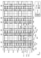
- FIG. 4 is a plan view of the memory cell array according to the first modification of the first embodiment.
- the layout structure of FIG. 4 is basically the same as the layout structure of FIG. However, in FIG. 4, the M1 wirings 62, 64, 66, and 68 corresponding to the bit lines BL0 to BL3 are aligned with respect to the nanosheet. Further, the M1 wirings 61, 63, 65, 67 that supply VSS are also aligned with respect to the nanosheet. Then, as the arrangement positions of the M1 wirings 61 to 68 are changed, the contact positions and the lengths of the local wirings are different from those in FIG.
- a fork sheet FET is used for the memory cell, and in the X direction, places where the distance between the transistors is wide and places where the distance between the transistors is narrow appear alternately. Therefore, if the bit lines BL are arranged at equal intervals, the positions of the bit lines BL with respect to the nanosheet are not aligned. On the other hand, in this modification, the arrangement positions of the bit line BL with respect to the nanosheet are aligned. As a result, the characteristics of each bit line BL can be made uniform.
- M1 wirings 69a, 69b, 69c for supplying VSS are additionally arranged in the space created by aligning the arrangement positions of the bit wire BL with respect to the nanosheet.
- the distances to the VSS wirings on both sides can be made uniform for any bit wire BL, so that the load capacitance for the bit wire BL can be made uniform. It is not necessary to additionally arrange the M1 wirings 69a, 69b, 69c for supplying VSS.
- the thick M1 wirings 61A, 65A, 69A may be arranged.
- FIG. 6 is a plan view of the memory cell array according to the second modification of the first embodiment.
- the layout structure of FIG. 6 is almost the same as the layout structure of FIG.
- the positions of the M1 wirings 61 and 62 are interchanged, and the positions of the M1 wirings 65 and 66 are interchanged.
- the positions of the bit wires BL are aligned with respect to the portion exposed from the gate wiring of the fork sheet. That is, the M1 wirings 62, 64, 66, and 68 corresponding to the bit lines BL0 to BL3 are all located on the side opposite to the side exposed from the gate wiring of the fork sheet.
- the characteristics of each bit line BL can be further aligned.
- FIGS. 8A to 8C are cross-sectional views of the memory cell array of FIG. 7 in the horizontal direction in a plan view.
- 8 (a) is a cross section of line X1-X1'
- FIG. 8 (b) is a cross section of line X2-X2'
- FIG. 8 (c) is a cross section of line X3-X3'.
- the transistors of the memory cells of each bit are arranged in the X direction and consist of two fork sheet FETs connected in parallel.
- the structure of the memory cells will be described by taking the memory cells M00 and M01 as an example.
- the memory cell M00 has nanosheets 111 and 112 composed of three sheets as a channel portion.
- the memory cell M01 has nanosheets 113 and 114 composed of three sheets as channel portions.
- pads 121a and 122a made of a semiconductor layer having an integral structure connected to three sheets are formed on the lower side of the drawings of the nanosheets 111 and 112, respectively.
- Pads 121b and 122b made of a semiconductor layer having an integral structure connected to three sheets are formed on the upper side of the drawings of the nanosheets 111 and 112, respectively.
- the pads 121a, 121b, 122a, 122b serve as nodes of the memory cell M00.
- Pads 123a and 124a made of a semiconductor layer having an integral structure connected to three sheets are formed on the lower side of the drawings of the nanosheets 113 and 114, respectively.
- Pads 123b and 124b made of a semiconductor layer having an integral structure connected to three sheets are formed on the upper side of the drawings of the nanosheets 113 and 114, respectively.
- the pads 123a, 123b, 124a, 124b serve as nodes of the memory cell M01.
- Gate wirings 131, 132, 133, 134 extending in the X direction are formed.
- the gate wiring 131 surrounds the outer periphery of the nanosheet 111 of the memory cell M00 in the X and Z directions via a gate insulating film (not shown).
- the gate wiring 132 surrounds the outer periphery of the nanosheet 112 of the memory cell M00 in the X and Z directions via a gate insulating film (not shown).
- the gate wirings 131 and 132 serve as gates for the memory cells M00.
- the gate wiring 133 surrounds the outer periphery of the nanosheet 113 of the memory cell M01 in the X and Z directions via a gate insulating film (not shown).
- the gate wiring 134 surrounds the outer periphery of the nanosheet 114 of the memory cell M01 in the X and Z directions via a gate insulating film (not shown).
- the gate wirings 133 and 134 serve as gates for the memory cell M01.
- the surface on the nanosheet 112 side in the X direction is not covered by the gate wiring 131, but is exposed from the gate wiring 131.
- the surface of the nanosheet 112 on the nanosheet 111 side in the X direction is not covered by the gate wiring 132 and is exposed from the gate wiring 132.
- the surface of the nanosheet 113 on the nanosheet 114 side in the X direction is not covered by the gate wiring 133 and is exposed from the gate wiring 133.
- the surface of the nanosheet 114 on the nanosheet 113 side in the X direction is not covered by the gate wiring 134 and is exposed from the gate wiring 134.
- the space required between the nanosheet 111 and the nanosheet 112 is reduced, so that the distance between the nanosheet 111 and the nanosheet 112 can be reduced.
- the space required between the nanosheet 113 and the nanosheet 114 is reduced, the distance between the nanosheet 113 and the nanosheet 114 can be reduced.
- the gate wiring 131 and the gate wiring 132 are connected by a bridge portion 135 formed between the gate wiring 131 and the gate wiring 132. Further, the gate wiring 133 and the gate wiring 134 are connected by a bridge portion 136 formed between the gate wiring 133 and the gate wiring 134.
- the bridge portions 135 and 136 are examples of gate connection portions.
- the local wiring 141, 142, 143, 144 extending in the X direction are formed.
- the local wiring 141 is connected to the pads 121a and 122a, and the local wiring 142 is connected to the pads 121b and 122b. That is, the drains of the two nanosheet FETs of the memory cell M00 are connected to each other, and the sources are connected to each other.
- the local wiring 143 is connected to the pads 123a and 124a
- the local wiring 144 is connected to the pads 123b and 124b. That is, the drains of the two nanosheet FETs of the memory cell M01 are connected to each other, and the sources are connected to each other.
- the local wiring 142 is connected to the M1 wiring 62 via the contact 151.
- the local wiring 144 is connected to the M1 wiring 64 via the contact 152.
- the contacts 171 and 172 determine the stored value of the memory cell depending on the presence or absence thereof.
- the contact 171 connects the local wiring 141 and the M1 wiring 61 that supplies VSS when formed.
- the contact 172 when formed, connects the local wire 143 to the M1 wire 63 that supplies VSS.
- the semiconductor storage device includes the ROM memory cell M00.
- the ROM memory cell M00 is provided between the bit wire 62 and the ground power supply wiring 61, and is provided between the first nanosheet FET having the nanosheet 111 as a channel region and between the bit wire 62 and the ground power supply wiring 61.
- a second nanosheet FET having a nanosheet 112 as a channel region is provided.
- the nanosheets 111 and 112 face each other in the X direction, the surface of the nanosheet 111 on the side of the nanosheet 112 in the X direction is exposed from the gate wiring 131, and the nanosheet 112 is on the side of the nanosheet 111 in the X direction. The surface is exposed from the gate wiring 132.
- the distance between the nanosheet 111 and the nanosheet 112 can be reduced, so that the size of the ROM memory cell M00 in the X direction can be reduced, and the area of the semiconductor storage device can be reduced.
- the distance between the ROM memory cells can be widened, so that the local wiring can be easily separated and the ease of manufacturing the semiconductor storage device is improved.
- bit wire BL is sandwiched between the VSS wirings, it is possible to prevent crosstalk between the bit wire BLs, so that malfunction can be suppressed. Further, since the distance from the bit wire BL to the VSS wiring on both sides is the same for all the bit wire BLs, the load capacitance due to the inter-wiring capacitance with respect to the bit wire BL will be the same. Therefore, performance variations such as operating speed between the bit lines BL are suppressed. Furthermore, since the arrangement positions of the bit wire BLs with respect to the nanosheets are aligned, the characteristics of each bit wire BL can be aligned.
- FIG. 9 is a plan view of the memory cell array according to the fourth modification of the first embodiment.
- the transistors of each memory cell are composed of two fork sheet FETs that are arranged adjacent to each other in the Y direction and share sources with each other.
- the structure of the memory cells will be described by taking the memory cells M00 and M01 as an example.
- the cross-sectional structure is the same as that of the first embodiment, and the cross-sectional view is omitted here.
- the memory cell M00 has nanosheets 211 and 212 composed of three sheets as a channel portion.
- the memory cell M01 has nanosheets 213 and 214 composed of three sheets as channel portions.
- a pad 221a made of a semiconductor layer having an integral structure connected to three sheets is formed on the lower side of the drawing of the nanosheet 211.
- Pads 221b made of a semiconductor layer having an integral structure connected to three sheets are formed between the nanosheets 211 and 212.
- a pad 221c made of a semiconductor layer having an integral structure connected to three sheets is formed on the upper side of the drawing of the nanosheet 212.
- the pads 221a and 221c serve as a drain area of the memory cell M00.
- the pad 221b serves as a source area of the memory cell M00.
- a pad 222a made of a semiconductor layer having an integral structure connected to three sheets is formed on the lower side of the drawing of the nanosheet 213.
- Pad 222b made of a semiconductor layer having an integral structure connected to three sheets is formed between the nanosheets 213 and 214.
- a pad 222c made of a semiconductor layer having an integral structure connected to three sheets is formed on the upper side of the drawing of the nanosheet 214.
- the pads 222a and 222c serve as a drain area of the memory cell M01.
- the pad 222b serves as a source area of the memory cell M01.
- Local wirings 241,242, 243, 244, 245, 246 extending in the X direction are formed.
- the local wiring 241 is connected to the pad 221a, the local wiring 242 is connected to the pad 221b, and the local wiring 243 is connected to the pad 221c.
- the local wiring 244 is connected to the pad 222a, the local wiring 245 is connected to the pad 222b, and the local wiring 246 is connected to the pad 222c.
- the local wiring 241 is connected to the M1 wiring 62 via the contact 251 and the local wiring 243 is connected to the M1 wiring 62 via the contact 252.
- the local wiring 244 is connected to the M1 wiring 64 via the contact 253, and the local wiring 246 is connected to the M1 wiring 64 via the contact 254.
- the contacts 271,272 determine the stored value of the memory cell depending on the presence or absence thereof.
- the contact 271 connects the local wiring 242 and the M1 wiring 61 that supplies VSS when formed.
- the surface of the nanosheet 211 on the nanosheet 213 side in the X direction is not covered by the gate wiring and is exposed from the gate wiring.
- the surface on the nanosheet 211 side in the X direction is not covered by the gate wiring and is exposed from the gate wiring.
- the surface on the nanosheet 214 side in the X direction is not covered by the gate wiring and is exposed from the gate wiring.
- the surface on the nanosheet 212 side in the X direction is not covered by the gate wiring and is exposed from the gate wiring.
- the space required between the nanosheets 211,212 and the nanosheets 213,214 is reduced, so that the distance between the nanosheets 211,212 and the nanosheets 213,214 can be reduced. Therefore, it is possible to reduce the area of the semiconductor storage device having the fork sheet FET.
- bit line BL With respect to the bit line BL, the same effect as that of the first embodiment can be obtained.
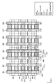
- FIG. 10 and 11 are views showing an example of the layout structure of the mask ROM according to the second embodiment
- FIG. 10 is a plan view of the memory cell array
- FIGS. 11 (a) to 11 (c) are views of the memory cell array of FIG. It is sectional drawing in the horizontal direction in a plan view.
- 11 (a) is a cross section of line X1-X1'
- FIG. 11 (b) is a cross section of line X2-X2'
- FIG. 11 (c) is a cross section of line X3-X3'.
- FIG. 10 corresponds to a layout for (4 ⁇ 4) bits.
- the broken line indicates the frame of the memory cell for one bit. That is, FIG. 10 shows a configuration in which four memory cells are arranged in the X direction and four in the Y direction. In the Y direction, the memory cells are arranged so as to be inverted in the Y direction every other row. For example, the two memory cells from the left in the bottom row of the drawing correspond to the memory cells M00 and M01 in the circuit diagram of FIG. 1, respectively.
- FIGS. 10 and 11 the components common to those in FIGS. 2 and 3 are designated by the same reference numerals as those in FIGS. 2 and 3, and detailed description thereof may be omitted here.
- the memory cells M00 and M01 have nanosheets 11A and 12A composed of three sheets, respectively, as channel portions. That is, the memory cells M00 and M01 include nanosheet FETs. Both surfaces of the nanosheet 11A in the X direction are covered with the gate wiring 31A. Both surfaces of the nanosheet 12A in the X direction are covered with the gate wiring 32A. Therefore, the distance between the nanosheets 11A and 12A is the same as the distance between the other nanosheets (d3).
- the M1 wirings 61 to 68 extending in the Y direction are arranged at equal intervals.
- the M1 wirings 62, 64, 66, 68 corresponding to the bit lines BL0 to BL3 are sandwiched between the M1 wirings 61, 63, 65, 67 that supply VSS.
- crosstalk between the bit wire BLs can be prevented, so that malfunction can be suppressed.
- the load capacitance due to the interwiring capacitance with respect to the bit wire BL is the same. Therefore, performance variations such as operating speed between the bit lines BL are suppressed.
- bit wire BL placement positions of the bit wire BL with respect to the nanosheet are aligned. As a result, the characteristics of each bit line BL can be made uniform.
- FIG. 12 is a plan view of the memory cell array according to the first modification of the second embodiment.
- the transistors of the memory cells of each bit are composed of two nanosheet FETs arranged in the Y direction and connected in parallel.
- the memory cell M00 has nanosheets 211A and 212A composed of three sheets as channel portions.
- the memory cell M01 has nanosheets 213A and 214A composed of three sheets as channel portions. Both surfaces of the nanosheets 211A, 212A, 213A, and 214A in the X direction are covered with gate wiring. Therefore, the spacing between the nanosheets 211A and 213A and the spacing between the nanosheets 212A and 214A are the same as the spacing between the other nanosheets, and the bit line BL has the same effect as that of the second embodiment. can get.
- FIG. 13 is a circuit diagram showing a configuration of a mask ROM as an example of a semiconductor storage device.
- the mask ROM of FIG. 13 indicates whether the source and drain of the memory cell transistor are connected to the same line of the bit line and the ground power supply wiring, or are connected to different lines. It corresponds to "0".
- the mask ROM includes a memory cell array 3A, a column decoder 2, and a sense amplifier 18.
- the gates of the memory cells Mij are connected to the word line WLi in common in the row direction.
- the source and drain of the memory cell Mij are connected to the bit line BLj or connected to the ground power supply wiring VSS.
- the stored data of the memory cell Mij is set to “0”, one of the source and the drain is connected to the bit line BLj and the other is connected to the ground power supply wiring VSS.
- the storage data of the memory cell Mij is set to "1”
- both the source and the drain are connected to the bit line BLj or the ground power supply wiring VSS.
- the column decoder 2 is composed of an N-type MOS transistor Cj.
- the drains are all connected in common, the gate is connected to the column selection signal line CLj, and the source is connected to the bit line BLj.
- the sense amplifier 18 includes a P-type MOS transistor 5 for precharging, an inverter 8 for determining the output data of the memory cell Mij, and an inverter 9 for buffering the output signal of the inverter 8.
- a precharge signal NPR is input to the gate of the P-type MOS transistor 5, a power supply voltage VDD is supplied to the source, and the drain is connected to the common drain of the N-type MOS transistor Cj.
- the inverter 8 receives the signal SIN of the common drain of the N-type MOS transistor Cj and determines the output data of the memory cell Mij.
- the inverter 9 receives the output signal SOUT of the inverter 8 and outputs the stored data of the memory cell Mij.
- the precharge signal NPR is changed from high level to low level, and the precharge P-type MOS transistor is turned on.
- one of the source and the drain is connected to the bit line BL0, and the other is connected to the ground power supply wiring VSS. Therefore, since a current flows from the bit line BL0 to the ground power supply wiring VSS via the memory cell M00, the input signal SIN of the inverter 8 becomes a voltage lower than the switching level of the inverter 8. Therefore, the output signal SOUT of the inverter 8 holds the high level, and the output signal OUT of the inverter 9 holds the low level.
- the word line WL1 is changed from the low level in the non-selected state to the high level in the selected state.
- both the source and the drain are connected to the bit line BL0. Therefore, since no current flows through the bit line BL0, the input signal SIN of the inverter 8 has a voltage higher than the switching level of the inverter 8. Therefore, the output signal SOUT of the inverter 8 becomes a low level, and the output signal OUT of the inverter 9 becomes a high level.
- the low level is output (storage data “0”), and the source and drain of the memory cell are output.
- the high level is output (stored data "1").
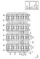
- FIG. 14 is a diagram showing an example of the layout structure of the mask ROM according to the third embodiment, and is a plan view of the memory cell array.
- FIG. 14 corresponds to a layout for (4 ⁇ 4) bits.
- the broken line indicates the frame of the memory cell for one bit. That is, FIG. 14 shows a configuration in which four memory cells are arranged in the X direction and four in the Y direction. For example, the two memory cells from the left in the bottom row of the drawing correspond to the memory cells M00 and M01 in the circuit diagram of FIG. 13, respectively.
- FIG. 14 is basically the same as the configuration of FIG. 2 shown in the first embodiment. However, due to the difference in the circuit structure of the mask ROM, there is a difference in the position of the contact and the like. Further, the dummy gate wiring for supplying VSS is not arranged. Hereinafter, the description of the same configuration as that of the first embodiment may be omitted. Further, the cross-sectional structure is the same as that in FIG. 3, and the cross-sectional view is omitted here.
- the memory cells M00 and M01 each have nanosheets 311, 312 composed of three sheets as channel portions. That is, the memory cells M00 and M01 include nanosheet FETs.
- the nanosheets 311, 312 face each other in the X direction.
- pads 321a and 322a made of a semiconductor layer having an integral structure connected to three sheets are formed on the lower side of the drawings of nanosheets 311, 312, respectively.
- Pads 321b and 322b made of a semiconductor layer having an integral structure connected to three sheets are formed on the upper side of the drawings of the nanosheets 311, 312, respectively.
- the pads 321a and 321b serve as nodes of the memory cell M00.
- the pads 322a and 322b serve as nodes of the memory cell M01.
- Gate wirings 331 and 332 extending in the X direction are formed.
- the gate wiring 331 surrounds the outer periphery of the nanosheet 311 of the memory cell M00 in the X and Z directions via a gate insulating film.
- the gate wiring 331 serves as a gate for the memory cell M00.
- the gate wiring 332 surrounds the outer periphery of the nanosheet 312 of the memory cell M01 in the X and Z directions with a gate insulating film.
- the gate wiring 332 serves as a gate for the memory cell M01.
- the gate wirings 331 and 332 are connected to other gate wirings arranged in a row in the X direction to form the word line WL0. That is, each of the word lines WL0 to WL3 includes gate wiring arranged in a row in the X direction.
- Local wiring 341, 342, 343, 344 extending in the X direction is formed.
- the local wiring 341 is connected to the pad 321a, and the local wiring 342 is connected to the pad 321b.
- the local wiring 343 is connected to the pad 322a, and the local wiring 344 is connected to the pad 322b.
- the contacts 371,372,373,374 determine the stored value of the memory cell according to the position. That is, the memory cells M00 and M01 store data “1” when both nodes are connected to VSS via the contact or when both nodes are connected to the bit line BL via the contact. Has. On the other hand, the memory cells M00 and M01 store data "0" when one node is connected to VSS via a contact and the other node is connected to bit line BL via a contact. Have.
- the memory cell M00 is connected to the M1 wiring 61 to which one node supplies VSS via the contact 371, and the other node contacts the M1 wiring 62 corresponding to the bit line BL0. Since it is connected via 372, it has stored data "0".
- the memory cell M01 is connected to the M1 wiring 63 to which one node supplies VSS via the contact 373, and the other node is connected to the M1 wiring 64 corresponding to the bit line BL1 via the contact 374. Therefore, it has stored data "0".
- the surface on the nanosheet 312 side in the X direction is not covered by the gate wiring 331 and is exposed from the gate wiring 331.
- the surface of the nanosheet 312 on the nanosheet 311 side in the X direction is not covered by the gate wiring 332 and is exposed from the gate wiring 332. That is, the memory cells M00 and M01 are fork sheet FETs.
- the gate wiring 331 and the gate wiring 332 are connected by a bridge portion 333 formed between the gate wiring 331 and the gate wiring 332.
- the bridge portion 333 is an example of a gate connection portion.
- the space required between the nanosheets 311 and the nanosheets 312 is reduced, so that the distance between the nanosheets 311 and the nanosheets 312 can be reduced. Therefore, it is possible to reduce the area of the semiconductor storage device having the fork sheet FET.
- the semiconductor storage device includes ROM memory cells M00 and M01 adjacent to each other in the X direction.
- the ROM memory cell M00 is provided between the bit line 62 and the ground power supply wiring 61, and includes a nanosheet FET having a nanosheet 311 as a channel region.
- the ROM memory cell M01 is provided between the bit line 64 and the ground power supply wiring 63, and includes a nanosheet FET having a nanosheet 312 as a channel region.
- the nanosheets 311, 312 face each other in the X direction, the surface of the nanosheet 311 on the side of the nanosheet 312 in the X direction is exposed from the gate wiring 331, and the nanosheet 312 is the surface on the side of the nanosheet 311 in the X direction. Is exposed from the gate wiring 332. As a result, the distance between the nanosheets 311 and the nanosheets 312 can be reduced, so that the area of the semiconductor storage device can be reduced.
- the M1 wirings 61 to 68 extending in the Y direction are arranged at equal intervals.
- the M1 wirings 62, 64, 66, 68 corresponding to the bit lines BL0 to BL3 are sandwiched between the M1 wirings 61, 63, 65, 67 that supply VSS.
- crosstalk between the bit wire BLs can be prevented, so that malfunction can be suppressed.
- the load capacitance due to the inter-wiring capacitance with respect to the bit wire BL is uniform. Therefore, performance variations such as operating speed between the bit lines BL are suppressed.
- the M1 wirings 61 to 68 extending in the Y direction do not have to be arranged at equal intervals. Even in this case, if the distance from the bit wire BL to the VSS wiring on both sides is the same for all the bit wire BLs, the load capacitance due to the interwiring capacitance with respect to the bit wire BL is the same, so that the operating speed between the bit wire BLs is the same. Performance variations such as are suppressed.
- FIG. 15 is a plan view of the memory cell array according to the first modification of the third embodiment.
- the layout structure of FIG. 15 is basically the same as the layout structure of FIG. However, in FIG. 15, the M1 wirings 62, 64, 66, and 68 corresponding to the bit lines BL0 to BL3 are aligned with respect to the nanosheet, as in the modified example 1 of the first embodiment. Further, the M1 wirings 61, 63, 65, 67 that supply VSS are also aligned with respect to the nanosheet. Then, as the arrangement positions of the M1 wirings 61 to 68 are changed, the contact positions and the lengths of the local wirings are different from those in FIG.
- M1 wirings 69a, 69b, 69c for supplying VSS are additionally arranged in the space created by aligning the arrangement positions of the bit wire BL with respect to the nanosheet. As a result, the distances to the VSS wirings on both sides can be made uniform for any bit wire BL, so that the load capacitance for the bit wire BL can be made uniform. It is not necessary to additionally arrange the M1 wirings 69a, 69b, 69c for supplying VSS.
- a thick M1 wiring may be arranged instead of the M1 wiring that supplies two adjacent VSSs.
- FIG. 16 is a plan view of the memory cell array according to the second modification of the third embodiment.
- the layout structure of FIG. 16 is almost the same as the layout structure of FIG.
- the positions of the M1 wirings 61 and 62 are interchanged, and the positions of the M1 wirings 65 and 66 are interchanged, as in the modified example 2 of the first embodiment.
- the positions of the bit wires BL are aligned with respect to the portion exposed from the gate wiring of the fork sheet. That is, the M1 wirings 62, 64, 66, and 68 corresponding to the bit lines BL0 to BL3 are all located on the side opposite to the side exposed from the gate wiring of the fork sheet.
- the characteristics of each bit line BL can be further aligned.
- FIG. 17 is a plan view of the memory cell array according to the third modification of the third embodiment.
- the transistors of the memory cells of each bit are composed of two fork sheet FETs arranged in the X direction and connected in parallel.
- the structure of the memory cells will be described by taking the memory cells M00 and M01 as an example.
- the memory cell M00 has nanosheets 411 and 412 composed of three sheets as a channel portion.
- the memory cell M01 has nanosheets 413 and 414 composed of three sheets as channel portions.
- pads 421a and 422a made of a semiconductor layer having an integral structure connected to three sheets are formed on the lower side of the drawings of nanosheets 411 and 412, respectively.
- Pads 421b and 422b made of a semiconductor layer having an integral structure connected to three sheets are formed on the upper side of the drawings of the nanosheets 411 and 412, respectively.
- Pads 421a, 421b, 422a, and 422b serve as nodes of memory cell M00.
- Pads 423a and 424a made of a semiconductor layer having an integral structure connected to three sheets are formed on the lower side of the drawings of the nanosheets 413 and 414, respectively.
- Pads 423b and 424b made of a semiconductor layer having an integral structure connected to three sheets are formed on the upper side of the drawings of the nanosheets 413 and 414, respectively.
- the pads 423a, 423b, 424a, and 424b serve as nodes of the memory cell M01.
- Gate wiring 431, 432, 433, 434 extending in the X direction is formed.
- the gate wiring 431 surrounds the outer periphery of the nanosheet 411 of the memory cell M00 in the X and Z directions via a gate insulating film (not shown).
- the gate wiring 432 surrounds the outer periphery of the nanosheet 412 of the memory cell M00 in the X and Z directions via a gate insulating film (not shown).
- the gate wirings 431 and 432 serve as the gate of the memory cell M00.
- the gate wiring 433 surrounds the outer periphery of the nanosheet 413 of the memory cell M01 in the X and Z directions via a gate insulating film (not shown).
- the gate wiring 434 surrounds the outer periphery of the nanosheet 414 of the memory cell M01 in the X and Z directions via a gate insulating film (not shown).
- the gate wirings 433 and 434 serve as gates for the memory cell M01.
- the surface on the nanosheet 412 side in the X direction is not covered by the gate wiring 431 and is exposed from the gate wiring 431.
- the surface on the nanosheet 411 side in the X direction is not covered by the gate wiring 432 and is exposed from the gate wiring 432.
- the surface of the nanosheet 413 on the nanosheet 414 side in the X direction is not covered by the gate wiring 433 and is exposed from the gate wiring 433.
- the surface of the nanosheet 414 on the nanosheet 413 side in the X direction is not covered by the gate wiring 434 and is exposed from the gate wiring 434.
- the space required between the nanosheets 411 and the nanosheets 412 is reduced, so that the distance between the nanosheets 411 and the nanosheets 412 can be reduced.
- the space required between the nanosheets 413 and the nanosheets 414 is reduced, the distance between the nanosheets 413 and the nanosheets 414 can be reduced.
- the gate wiring 431 and the gate wiring 432 are connected by a bridge portion 435 formed between the gate wiring 431 and the gate wiring 432.
- the gate wiring 433 and the gate wiring 434 are connected by a bridge portion 436 formed between the gate wiring 433 and the gate wiring 434.
- the bridge portions 435 and 436 are examples of gate connection portions.
- Local wiring 441, 442, 443, 444 extending in the X direction is formed.
- the local wiring 441 is connected to the pads 421a and 422a, and the local wiring 442 is connected to the pads 421b and 422b. That is, the drains of the two nanosheet FETs of the memory cell M00 are connected to each other, and the sources are connected to each other.
- the local wiring 443 is connected to the pads 423a and 424a, and the local wiring 444 is connected to the pads 423b and 424b. That is, the drains of the two nanosheet FETs of the memory cell M01 are connected to each other, and the sources are connected to each other.
- the contacts 471, 472, 473, 474 determine the stored value of the memory cell according to the position. That is, the memory cells M00 and M01 store data “1” when both nodes are connected to VSS via the contact or when both nodes are connected to the bit line BL via the contact. Has. On the other hand, the memory cells M00 and M01 store data "0" when one node is connected to VSS via a contact and the other node is connected to bit line BL via a contact. Have.
- the memory cell M00 is connected to the M1 wiring 61 to which one node supplies VSS via the contact 471, and the other node contacts the M1 wiring 62 corresponding to the bit line BL0. Since it is connected via 472, it has stored data "0".
- the memory cell M01 is connected to the M1 wiring 63 to which one node supplies VSS via the contact 473, and the other node is connected to the M1 wiring 64 corresponding to the bit line BL1 via the contact 474. Therefore, it has stored data "0".
- the semiconductor storage device includes the ROM memory cell M00.
- the ROM memory cell M00 is provided between the bit wire 62 and the ground power supply wiring 61, and is provided between the first nanosheet FET having the nanosheet 411 as a channel region and between the bit wire 62 and the ground power supply wiring 61. It is provided with a second nanosheet FET having a nanosheet 412 as a channel region.
- the nanosheets 411 and 412 face each other in the X direction, the surface of the nanosheet 411 on the side of the nanosheet 412 in the X direction is exposed from the gate wiring 431, and the nanosheet 112 is the surface on the side of the nanosheet 411 in the X direction. Is exposed from the gate wiring 432.
- the distance between the nanosheets 411 and the nanosheets 412 can be reduced, so that the size of the ROM memory cell M00 in the X direction can be reduced, and the area of the semiconductor storage device can be reduced.
- the distance between the ROM memory cells can be widened, so that the local wiring can be easily separated and the ease of manufacturing the semiconductor storage device is improved.
- bit wire BL is sandwiched between the VSS wirings, it is possible to prevent crosstalk between the bit wire BLs, so that malfunction can be suppressed. Further, since the distance from the bit wire BL to the VSS wiring on both sides is the same for all the bit wire BLs, the load capacitance due to the interwiring capacitance with respect to the bit wire BL is the same. Therefore, performance variations such as operating speed between the bit lines BL are suppressed. Furthermore, since the arrangement positions of the bit wire BLs with respect to the nanosheets are aligned, the characteristics of each bit wire BL can be aligned.
- FIG. 18 is a diagram showing an example of the layout structure of the mask ROM according to the fourth embodiment, and is a plan view of the memory cell array.
- FIG. 18 corresponds to a layout for (4 ⁇ 4) bits.
- the broken line indicates the frame of the memory cell for one bit. That is, FIG. 18 shows a configuration in which four memory cells are arranged in the X direction and four in the Y direction. For example, the two memory cells from the left in the bottom row of the drawing correspond to the memory cells M00 and M01 in the circuit diagram of FIG. 13, respectively.
- the memory cells M00 and M01 have nanosheets 311A and 312A composed of three sheets, respectively, as channel portions. That is, the memory cells M00 and M01 include nanosheet FETs. Both surfaces of the nanosheet 311A in the X direction are covered with the gate wiring 331A. Both sides of the nanosheet 312A in the X direction are covered with the gate wiring 332A. Therefore, the distance between the nanosheets 311A and 312A is the same as the distance between the other nanosheets.
- the M1 wirings 61 to 68 extending in the Y direction are arranged at equal intervals.
- the M1 wirings 62, 64, 66, 68 corresponding to the bit lines BL0 to BL3 are sandwiched between the M1 wirings 61, 63, 65, 67 that supply VSS.
- crosstalk between the bit wire BLs can be prevented, so that malfunction can be suppressed.
- the load capacitance due to the interwiring capacitance with respect to the bit wire BL is the same. Therefore, performance variations such as operating speed between the bit lines BL are suppressed.
- bit wire BL placement positions of the bit wire BL with respect to the nanosheet are aligned. As a result, the characteristics of each bit line BL can be made uniform.
- each nanosheet has a structure of three sheets, but the present invention is not limited to this, and a part or all of the nanosheets may be one, two, or the like. It may have a sheet structure of four or more sheets.
- the cross-sectional shape of the nanosheet is rectangular, but the present invention is not limited to this. For example, it may be square, circular, oval, or the like.
- a layout structure having a small area can be realized for a semiconductor storage device using a fork sheet FET, which is useful for, for example, miniaturization of a semiconductor chip and improvement of the degree of integration.
Landscapes
- Semiconductor Memories (AREA)
- Chemical & Material Sciences (AREA)
- Engineering & Computer Science (AREA)
- Crystallography & Structural Chemistry (AREA)
- Nanotechnology (AREA)
Priority Applications (3)
| Application Number | Priority Date | Filing Date | Title |
|---|---|---|---|
| CN202080087274.2A CN114868242B (zh) | 2019-12-20 | 2020-12-14 | 半导体存储装置 |
| JP2021565573A JP7610131B2 (ja) | 2019-12-20 | 2020-12-14 | 半導体記憶装置 |
| US17/842,473 US12279419B2 (en) | 2019-12-20 | 2022-06-16 | Semiconductor storage device having rom cells including nanosheet field effect transistors |
Applications Claiming Priority (2)
| Application Number | Priority Date | Filing Date | Title |
|---|---|---|---|
| JP2019230713 | 2019-12-20 | ||
| JP2019-230713 | 2019-12-20 |
Related Child Applications (1)
| Application Number | Title | Priority Date | Filing Date |
|---|---|---|---|
| US17/842,473 Continuation US12279419B2 (en) | 2019-12-20 | 2022-06-16 | Semiconductor storage device having rom cells including nanosheet field effect transistors |
Publications (1)
| Publication Number | Publication Date |
|---|---|
| WO2021125138A1 true WO2021125138A1 (ja) | 2021-06-24 |
Family
ID=76477544
Family Applications (1)
| Application Number | Title | Priority Date | Filing Date |
|---|---|---|---|
| PCT/JP2020/046574 Ceased WO2021125138A1 (ja) | 2019-12-20 | 2020-12-14 | 半導体記憶装置 |
Country Status (4)
| Country | Link |
|---|---|
| US (1) | US12279419B2 (https=) |
| JP (1) | JP7610131B2 (https=) |
| CN (1) | CN114868242B (https=) |
| WO (1) | WO2021125138A1 (https=) |
Cited By (3)
| Publication number | Priority date | Publication date | Assignee | Title |
|---|---|---|---|---|
| US20230096892A1 (en) * | 2021-09-29 | 2023-03-30 | Advanced Micro Devices, Inc. | Cross fet sram cell layout |
| US11881393B2 (en) | 2021-09-29 | 2024-01-23 | Advanced Micro Devices, Inc. | Cross field effect transistor library cell architecture design |
| WO2026009666A1 (ja) * | 2024-07-04 | 2026-01-08 | 株式会社ソシオネクスト | 半導体記憶装置 |
Families Citing this family (4)
| Publication number | Priority date | Publication date | Assignee | Title |
|---|---|---|---|---|
| JP7640861B2 (ja) * | 2019-10-18 | 2025-03-06 | 株式会社ソシオネクスト | 半導体集積回路装置 |
| US20220359545A1 (en) * | 2021-05-07 | 2022-11-10 | Taiwan Semiconductor Manufacturing Company, Ltd. | Semiconductor memory devices with dielectric fin structures |
| US12598741B2 (en) * | 2023-01-30 | 2026-04-07 | Arm Limited | Multi-stack bitcell architecture |
| US12580033B2 (en) * | 2023-07-03 | 2026-03-17 | Taiwan Semiconductor Manufacturing Company, Ltd. | Read-only memory method, layout, and device |
Citations (4)
| Publication number | Priority date | Publication date | Assignee | Title |
|---|---|---|---|---|
| US20160329313A1 (en) * | 2014-06-23 | 2016-11-10 | Synopsys, Inc. | Cells having transistors and interconnects including nanowires or 2d material strips |
| US20180233508A1 (en) * | 2016-06-01 | 2018-08-16 | Taiwan Semiconductor Manufacturing Co., Ltd. | Read-only memory (rom) device structure and method for forming the same |
| WO2019116827A1 (ja) * | 2017-12-12 | 2019-06-20 | ソニーセミコンダクタソリューションズ株式会社 | 半導体装置及びその製造方法 |
| WO2019220983A1 (ja) * | 2018-05-17 | 2019-11-21 | 株式会社ソシオネクスト | 半導体集積回路装置 |
Family Cites Families (8)
| Publication number | Priority date | Publication date | Assignee | Title |
|---|---|---|---|---|
| JP2009054707A (ja) * | 2007-08-24 | 2009-03-12 | Renesas Technology Corp | 半導体記憶装置およびその製造方法 |
| JP4751432B2 (ja) * | 2008-09-26 | 2011-08-17 | シャープ株式会社 | 半導体記憶装置 |
| US10381100B2 (en) * | 2016-07-01 | 2019-08-13 | Synopsys, Inc. | Enhancing memory yield and performance through utilizing nanowire self-heating |
| CN109390021B (zh) * | 2017-08-03 | 2022-05-03 | 联华电子股份有限公司 | 只读存储器 |
| SG11202005030XA (en) * | 2017-11-28 | 2020-06-29 | Univ Texas | Catalyst influenced pattern transfer technology |
| US10833078B2 (en) * | 2017-12-04 | 2020-11-10 | Tokyo Electron Limited | Semiconductor apparatus having stacked gates and method of manufacture thereof |
| US11355504B2 (en) * | 2018-05-31 | 2022-06-07 | Intel Corporation | Anti-ferroelectric capacitor memory cell |
| US11139300B2 (en) * | 2019-11-20 | 2021-10-05 | Intel Corporation | Three-dimensional memory arrays with layer selector transistors |
-
2020
- 2020-12-14 CN CN202080087274.2A patent/CN114868242B/zh active Active
- 2020-12-14 JP JP2021565573A patent/JP7610131B2/ja active Active
- 2020-12-14 WO PCT/JP2020/046574 patent/WO2021125138A1/ja not_active Ceased
-
2022
- 2022-06-16 US US17/842,473 patent/US12279419B2/en active Active
Patent Citations (4)
| Publication number | Priority date | Publication date | Assignee | Title |
|---|---|---|---|---|
| US20160329313A1 (en) * | 2014-06-23 | 2016-11-10 | Synopsys, Inc. | Cells having transistors and interconnects including nanowires or 2d material strips |
| US20180233508A1 (en) * | 2016-06-01 | 2018-08-16 | Taiwan Semiconductor Manufacturing Co., Ltd. | Read-only memory (rom) device structure and method for forming the same |
| WO2019116827A1 (ja) * | 2017-12-12 | 2019-06-20 | ソニーセミコンダクタソリューションズ株式会社 | 半導体装置及びその製造方法 |
| WO2019220983A1 (ja) * | 2018-05-17 | 2019-11-21 | 株式会社ソシオネクスト | 半導体集積回路装置 |
Cited By (5)
| Publication number | Priority date | Publication date | Assignee | Title |
|---|---|---|---|---|
| US20230096892A1 (en) * | 2021-09-29 | 2023-03-30 | Advanced Micro Devices, Inc. | Cross fet sram cell layout |
| US11778803B2 (en) * | 2021-09-29 | 2023-10-03 | Advanced Micro Devices, Inc. | Cross FET SRAM cell layout |
| US11881393B2 (en) | 2021-09-29 | 2024-01-23 | Advanced Micro Devices, Inc. | Cross field effect transistor library cell architecture design |
| US12274046B2 (en) | 2021-09-29 | 2025-04-08 | Advanced Micro Devices, Inc. | Cross FET SRAM cell layout |
| WO2026009666A1 (ja) * | 2024-07-04 | 2026-01-08 | 株式会社ソシオネクスト | 半導体記憶装置 |
Also Published As
| Publication number | Publication date |
|---|---|
| CN114868242A (zh) | 2022-08-05 |
| CN114868242B (zh) | 2024-11-12 |
| JPWO2021125138A1 (https=) | 2021-06-24 |
| US20220310634A1 (en) | 2022-09-29 |
| JP7610131B2 (ja) | 2025-01-08 |
| US12279419B2 (en) | 2025-04-15 |
Similar Documents
| Publication | Publication Date | Title |
|---|---|---|
| JP7610131B2 (ja) | 半導体記憶装置 | |
| KR101161506B1 (ko) | 듀얼 포트 sram을 위한 셀 구조 | |
| KR100423896B1 (ko) | 축소가능한 2개의 트랜지스터 기억 소자 | |
| KR100577610B1 (ko) | 반도체 장치, 반도체 장치의 제조 방법 및 에스램 장치,에스램 장치 제조 방법. | |
| TWI681542B (zh) | 靜態隨機存取記憶體的佈局圖案 | |
| CN107026168B (zh) | 集成电路结构 | |
| US10381056B2 (en) | Dual port static random access memory (DPSRAM) cell | |
| US7304874B2 (en) | Compact ternary and binary CAM bitcell architecture with no enclosed diffusion areas | |
| US12225719B2 (en) | Semiconductor storage device | |
| US20250151267A1 (en) | Semiconductor memory device | |
| US7259977B2 (en) | Semiconductor device having hierarchized bit lines | |
| TW201803086A (zh) | 靜態隨機存取記憶體的佈局圖案 | |
| US12277980B2 (en) | Semiconductor storage device | |
| US12396167B2 (en) | Semiconductor storage device | |
| US20240395709A1 (en) | Semiconductor memory device | |
| US20240331755A1 (en) | High-density memory cells and layouts thereof | |
| KR100665853B1 (ko) | 고집적 스태이틱 랜덤 억세스 메모리에 채용하기 적합한적층 메모리 셀 | |
| TWI845102B (zh) | 記憶體裝置和記憶體結構 | |
| TW202439919A (zh) | 記憶體裝置 | |
| KR0178815B1 (ko) | 레벨간 절연층에서 선택적으로 신장하는 디지트 라인을 갖는 반도체 ram 장치 | |
| WO2026009666A1 (ja) | 半導体記憶装置 | |
| WO2023004947A1 (zh) | 字线驱动器电路及存储器 | |
| JP2006245083A (ja) | 半導体集積回路 | |
| JP2010067677A (ja) | 半導体記憶装置 | |
| KR20050082454A (ko) | 축소가능한 2개의 트랜지스터 메모리(sttm) 셀의레이아웃 구조 |
Legal Events
| Date | Code | Title | Description |
|---|---|---|---|
| 121 | Ep: the epo has been informed by wipo that ep was designated in this application |
Ref document number: 20902583 Country of ref document: EP Kind code of ref document: A1 |
|
| ENP | Entry into the national phase |
Ref document number: 2021565573 Country of ref document: JP Kind code of ref document: A |
|
| NENP | Non-entry into the national phase |
Ref country code: DE |
|
| 122 | Ep: pct application non-entry in european phase |
Ref document number: 20902583 Country of ref document: EP Kind code of ref document: A1 |