WO2021125017A1 - Élément de réception de lumière et dispositif électroluminescent - Google Patents
Élément de réception de lumière et dispositif électroluminescent Download PDFInfo
- Publication number
- WO2021125017A1 WO2021125017A1 PCT/JP2020/045876 JP2020045876W WO2021125017A1 WO 2021125017 A1 WO2021125017 A1 WO 2021125017A1 JP 2020045876 W JP2020045876 W JP 2020045876W WO 2021125017 A1 WO2021125017 A1 WO 2021125017A1
- Authority
- WO
- WIPO (PCT)
- Prior art keywords
- light receiving
- region
- light
- regions
- wiring
- Prior art date
Links
- 230000003287 optical effect Effects 0.000 claims description 18
- 239000004065 semiconductor Substances 0.000 description 117
- 238000005304 joining Methods 0.000 description 11
- 239000000463 material Substances 0.000 description 11
- 229910052751 metal Inorganic materials 0.000 description 10
- 239000002184 metal Substances 0.000 description 10
- 230000001681 protective effect Effects 0.000 description 10
- 239000000919 ceramic Substances 0.000 description 6
- 230000012447 hatching Effects 0.000 description 6
- 238000000034 method Methods 0.000 description 6
- 238000009826 distribution Methods 0.000 description 5
- 229910052782 aluminium Inorganic materials 0.000 description 3
- XAGFODPZIPBFFR-UHFFFAOYSA-N aluminium Chemical compound [Al] XAGFODPZIPBFFR-UHFFFAOYSA-N 0.000 description 3
- PMHQVHHXPFUNSP-UHFFFAOYSA-M copper(1+);methylsulfanylmethane;bromide Chemical compound Br[Cu].CSC PMHQVHHXPFUNSP-UHFFFAOYSA-M 0.000 description 3
- 239000011521 glass Substances 0.000 description 3
- 229910052594 sapphire Inorganic materials 0.000 description 3
- 239000010980 sapphire Substances 0.000 description 3
- RYGMFSIKBFXOCR-UHFFFAOYSA-N Copper Chemical compound [Cu] RYGMFSIKBFXOCR-UHFFFAOYSA-N 0.000 description 2
- XEEYBQQBJWHFJM-UHFFFAOYSA-N Iron Chemical compound [Fe] XEEYBQQBJWHFJM-UHFFFAOYSA-N 0.000 description 2
- 229910052581 Si3N4 Inorganic materials 0.000 description 2
- 239000002131 composite material Substances 0.000 description 2
- 229910052802 copper Inorganic materials 0.000 description 2
- 239000010949 copper Substances 0.000 description 2
- -1 for example Substances 0.000 description 2
- 150000004767 nitrides Chemical class 0.000 description 2
- HBMJWWWQQXIZIP-UHFFFAOYSA-N silicon carbide Chemical compound [Si+]#[C-] HBMJWWWQQXIZIP-UHFFFAOYSA-N 0.000 description 2
- 229910010271 silicon carbide Inorganic materials 0.000 description 2
- HQVNEWCFYHHQES-UHFFFAOYSA-N silicon nitride Chemical compound N12[Si]34N5[Si]62N3[Si]51N64 HQVNEWCFYHHQES-UHFFFAOYSA-N 0.000 description 2
- 238000002834 transmittance Methods 0.000 description 2
- 229910002704 AlGaN Inorganic materials 0.000 description 1
- 229910000980 Aluminium gallium arsenide Inorganic materials 0.000 description 1
- 229910001218 Gallium arsenide Inorganic materials 0.000 description 1
- BQCADISMDOOEFD-UHFFFAOYSA-N Silver Chemical compound [Ag] BQCADISMDOOEFD-UHFFFAOYSA-N 0.000 description 1
- 241000826860 Trapezium Species 0.000 description 1
- 239000005388 borosilicate glass Substances 0.000 description 1
- 239000003086 colorant Substances 0.000 description 1
- WUUZKBJEUBFVMV-UHFFFAOYSA-N copper molybdenum Chemical compound [Cu].[Mo] WUUZKBJEUBFVMV-UHFFFAOYSA-N 0.000 description 1
- SBYXRAKIOMOBFF-UHFFFAOYSA-N copper tungsten Chemical compound [Cu].[W] SBYXRAKIOMOBFF-UHFFFAOYSA-N 0.000 description 1
- 230000006866 deterioration Effects 0.000 description 1
- 239000010432 diamond Substances 0.000 description 1
- 229910003460 diamond Inorganic materials 0.000 description 1
- 239000000428 dust Substances 0.000 description 1
- PCHJSUWPFVWCPO-UHFFFAOYSA-N gold Chemical compound [Au] PCHJSUWPFVWCPO-UHFFFAOYSA-N 0.000 description 1
- 229910052737 gold Inorganic materials 0.000 description 1
- 239000010931 gold Substances 0.000 description 1
- 230000017525 heat dissipation Effects 0.000 description 1
- 229910052742 iron Inorganic materials 0.000 description 1
- 238000004519 manufacturing process Methods 0.000 description 1
- 150000002739 metals Chemical class 0.000 description 1
- TWNQGVIAIRXVLR-UHFFFAOYSA-N oxo(oxoalumanyloxy)alumane Chemical compound O=[Al]O[Al]=O TWNQGVIAIRXVLR-UHFFFAOYSA-N 0.000 description 1
- 239000010453 quartz Substances 0.000 description 1
- 238000007789 sealing Methods 0.000 description 1
- VYPSYNLAJGMNEJ-UHFFFAOYSA-N silicon dioxide Inorganic materials O=[Si]=O VYPSYNLAJGMNEJ-UHFFFAOYSA-N 0.000 description 1
- 229910052709 silver Inorganic materials 0.000 description 1
- 239000004332 silver Substances 0.000 description 1
Images


Classifications
-
- H—ELECTRICITY
- H01—ELECTRIC ELEMENTS
- H01S—DEVICES USING THE PROCESS OF LIGHT AMPLIFICATION BY STIMULATED EMISSION OF RADIATION [LASER] TO AMPLIFY OR GENERATE LIGHT; DEVICES USING STIMULATED EMISSION OF ELECTROMAGNETIC RADIATION IN WAVE RANGES OTHER THAN OPTICAL
- H01S5/00—Semiconductor lasers
- H01S5/02—Structural details or components not essential to laser action
- H01S5/022—Mountings; Housings
- H01S5/023—Mount members, e.g. sub-mount members
- H01S5/02325—Mechanically integrated components on mount members or optical micro-benches
-
- H—ELECTRICITY
- H01—ELECTRIC ELEMENTS
- H01L—SEMICONDUCTOR DEVICES NOT COVERED BY CLASS H10
- H01L25/00—Assemblies consisting of a plurality of individual semiconductor or other solid state devices ; Multistep manufacturing processes thereof
- H01L25/03—Assemblies consisting of a plurality of individual semiconductor or other solid state devices ; Multistep manufacturing processes thereof all the devices being of a type provided for in the same subgroup of groups H01L27/00 - H01L33/00, or in a single subclass of H10K, H10N, e.g. assemblies of rectifier diodes
- H01L25/04—Assemblies consisting of a plurality of individual semiconductor or other solid state devices ; Multistep manufacturing processes thereof all the devices being of a type provided for in the same subgroup of groups H01L27/00 - H01L33/00, or in a single subclass of H10K, H10N, e.g. assemblies of rectifier diodes the devices not having separate containers
- H01L25/041—Assemblies consisting of a plurality of individual semiconductor or other solid state devices ; Multistep manufacturing processes thereof all the devices being of a type provided for in the same subgroup of groups H01L27/00 - H01L33/00, or in a single subclass of H10K, H10N, e.g. assemblies of rectifier diodes the devices not having separate containers the devices being of a type provided for in group H01L31/00
- H01L25/042—Assemblies consisting of a plurality of individual semiconductor or other solid state devices ; Multistep manufacturing processes thereof all the devices being of a type provided for in the same subgroup of groups H01L27/00 - H01L33/00, or in a single subclass of H10K, H10N, e.g. assemblies of rectifier diodes the devices not having separate containers the devices being of a type provided for in group H01L31/00 the devices being arranged next to each other
-
- H—ELECTRICITY
- H01—ELECTRIC ELEMENTS
- H01L—SEMICONDUCTOR DEVICES NOT COVERED BY CLASS H10
- H01L24/00—Arrangements for connecting or disconnecting semiconductor or solid-state bodies; Methods or apparatus related thereto
- H01L24/01—Means for bonding being attached to, or being formed on, the surface to be connected, e.g. chip-to-package, die-attach, "first-level" interconnects; Manufacturing methods related thereto
- H01L24/42—Wire connectors; Manufacturing methods related thereto
- H01L24/47—Structure, shape, material or disposition of the wire connectors after the connecting process
- H01L24/48—Structure, shape, material or disposition of the wire connectors after the connecting process of an individual wire connector
-
- H—ELECTRICITY
- H01—ELECTRIC ELEMENTS
- H01L—SEMICONDUCTOR DEVICES NOT COVERED BY CLASS H10
- H01L31/00—Semiconductor devices sensitive to infrared radiation, light, electromagnetic radiation of shorter wavelength or corpuscular radiation and specially adapted either for the conversion of the energy of such radiation into electrical energy or for the control of electrical energy by such radiation; Processes or apparatus specially adapted for the manufacture or treatment thereof or of parts thereof; Details thereof
- H01L31/02—Details
- H01L31/02002—Arrangements for conducting electric current to or from the device in operations
- H01L31/02005—Arrangements for conducting electric current to or from the device in operations for device characterised by at least one potential jump barrier or surface barrier
-
- H—ELECTRICITY
- H01—ELECTRIC ELEMENTS
- H01L—SEMICONDUCTOR DEVICES NOT COVERED BY CLASS H10
- H01L31/00—Semiconductor devices sensitive to infrared radiation, light, electromagnetic radiation of shorter wavelength or corpuscular radiation and specially adapted either for the conversion of the energy of such radiation into electrical energy or for the control of electrical energy by such radiation; Processes or apparatus specially adapted for the manufacture or treatment thereof or of parts thereof; Details thereof
- H01L31/12—Semiconductor devices sensitive to infrared radiation, light, electromagnetic radiation of shorter wavelength or corpuscular radiation and specially adapted either for the conversion of the energy of such radiation into electrical energy or for the control of electrical energy by such radiation; Processes or apparatus specially adapted for the manufacture or treatment thereof or of parts thereof; Details thereof structurally associated with, e.g. formed in or on a common substrate with, one or more electric light sources, e.g. electroluminescent light sources, and electrically or optically coupled thereto
- H01L31/14—Semiconductor devices sensitive to infrared radiation, light, electromagnetic radiation of shorter wavelength or corpuscular radiation and specially adapted either for the conversion of the energy of such radiation into electrical energy or for the control of electrical energy by such radiation; Processes or apparatus specially adapted for the manufacture or treatment thereof or of parts thereof; Details thereof structurally associated with, e.g. formed in or on a common substrate with, one or more electric light sources, e.g. electroluminescent light sources, and electrically or optically coupled thereto the light source or sources being controlled by the semiconductor device sensitive to radiation, e.g. image converters, image amplifiers or image storage devices
- H01L31/141—Semiconductor devices sensitive to infrared radiation, light, electromagnetic radiation of shorter wavelength or corpuscular radiation and specially adapted either for the conversion of the energy of such radiation into electrical energy or for the control of electrical energy by such radiation; Processes or apparatus specially adapted for the manufacture or treatment thereof or of parts thereof; Details thereof structurally associated with, e.g. formed in or on a common substrate with, one or more electric light sources, e.g. electroluminescent light sources, and electrically or optically coupled thereto the light source or sources being controlled by the semiconductor device sensitive to radiation, e.g. image converters, image amplifiers or image storage devices the semiconductor device sensitive to radiation being without a potential-jump barrier or surface barrier
- H01L31/143—Semiconductor devices sensitive to infrared radiation, light, electromagnetic radiation of shorter wavelength or corpuscular radiation and specially adapted either for the conversion of the energy of such radiation into electrical energy or for the control of electrical energy by such radiation; Processes or apparatus specially adapted for the manufacture or treatment thereof or of parts thereof; Details thereof structurally associated with, e.g. formed in or on a common substrate with, one or more electric light sources, e.g. electroluminescent light sources, and electrically or optically coupled thereto the light source or sources being controlled by the semiconductor device sensitive to radiation, e.g. image converters, image amplifiers or image storage devices the semiconductor device sensitive to radiation being without a potential-jump barrier or surface barrier the light source being a semiconductor device with at least one potential-jump barrier or surface barrier, e.g. light emitting diode
-
- H—ELECTRICITY
- H01—ELECTRIC ELEMENTS
- H01S—DEVICES USING THE PROCESS OF LIGHT AMPLIFICATION BY STIMULATED EMISSION OF RADIATION [LASER] TO AMPLIFY OR GENERATE LIGHT; DEVICES USING STIMULATED EMISSION OF ELECTROMAGNETIC RADIATION IN WAVE RANGES OTHER THAN OPTICAL
- H01S5/00—Semiconductor lasers
- H01S5/02—Structural details or components not essential to laser action
- H01S5/022—Mountings; Housings
- H01S5/02208—Mountings; Housings characterised by the shape of the housings
-
- H—ELECTRICITY
- H01—ELECTRIC ELEMENTS
- H01S—DEVICES USING THE PROCESS OF LIGHT AMPLIFICATION BY STIMULATED EMISSION OF RADIATION [LASER] TO AMPLIFY OR GENERATE LIGHT; DEVICES USING STIMULATED EMISSION OF ELECTROMAGNETIC RADIATION IN WAVE RANGES OTHER THAN OPTICAL
- H01S5/00—Semiconductor lasers
- H01S5/02—Structural details or components not essential to laser action
- H01S5/022—Mountings; Housings
- H01S5/0225—Out-coupling of light
- H01S5/02255—Out-coupling of light using beam deflecting elements
-
- H—ELECTRICITY
- H01—ELECTRIC ELEMENTS
- H01S—DEVICES USING THE PROCESS OF LIGHT AMPLIFICATION BY STIMULATED EMISSION OF RADIATION [LASER] TO AMPLIFY OR GENERATE LIGHT; DEVICES USING STIMULATED EMISSION OF ELECTROMAGNETIC RADIATION IN WAVE RANGES OTHER THAN OPTICAL
- H01S5/00—Semiconductor lasers
- H01S5/02—Structural details or components not essential to laser action
- H01S5/022—Mountings; Housings
- H01S5/023—Mount members, e.g. sub-mount members
- H01S5/02315—Support members, e.g. bases or carriers
-
- H—ELECTRICITY
- H01—ELECTRIC ELEMENTS
- H01S—DEVICES USING THE PROCESS OF LIGHT AMPLIFICATION BY STIMULATED EMISSION OF RADIATION [LASER] TO AMPLIFY OR GENERATE LIGHT; DEVICES USING STIMULATED EMISSION OF ELECTROMAGNETIC RADIATION IN WAVE RANGES OTHER THAN OPTICAL
- H01S5/00—Semiconductor lasers
- H01S5/06—Arrangements for controlling the laser output parameters, e.g. by operating on the active medium
- H01S5/068—Stabilisation of laser output parameters
- H01S5/0683—Stabilisation of laser output parameters by monitoring the optical output parameters
-
- H—ELECTRICITY
- H01—ELECTRIC ELEMENTS
- H01S—DEVICES USING THE PROCESS OF LIGHT AMPLIFICATION BY STIMULATED EMISSION OF RADIATION [LASER] TO AMPLIFY OR GENERATE LIGHT; DEVICES USING STIMULATED EMISSION OF ELECTROMAGNETIC RADIATION IN WAVE RANGES OTHER THAN OPTICAL
- H01S5/00—Semiconductor lasers
- H01S5/40—Arrangement of two or more semiconductor lasers, not provided for in groups H01S5/02 - H01S5/30
- H01S5/4025—Array arrangements, e.g. constituted by discrete laser diodes or laser bar
- H01S5/4031—Edge-emitting structures
-
- H—ELECTRICITY
- H01—ELECTRIC ELEMENTS
- H01L—SEMICONDUCTOR DEVICES NOT COVERED BY CLASS H10
- H01L2224/00—Indexing scheme for arrangements for connecting or disconnecting semiconductor or solid-state bodies and methods related thereto as covered by H01L24/00
- H01L2224/01—Means for bonding being attached to, or being formed on, the surface to be connected, e.g. chip-to-package, die-attach, "first-level" interconnects; Manufacturing methods related thereto
- H01L2224/42—Wire connectors; Manufacturing methods related thereto
- H01L2224/47—Structure, shape, material or disposition of the wire connectors after the connecting process
- H01L2224/48—Structure, shape, material or disposition of the wire connectors after the connecting process of an individual wire connector
- H01L2224/481—Disposition
- H01L2224/48151—Connecting between a semiconductor or solid-state body and an item not being a semiconductor or solid-state body, e.g. chip-to-substrate, chip-to-passive
- H01L2224/48221—Connecting between a semiconductor or solid-state body and an item not being a semiconductor or solid-state body, e.g. chip-to-substrate, chip-to-passive the body and the item being stacked
- H01L2224/48225—Connecting between a semiconductor or solid-state body and an item not being a semiconductor or solid-state body, e.g. chip-to-substrate, chip-to-passive the body and the item being stacked the item being non-metallic, e.g. insulating substrate with or without metallisation
- H01L2224/48227—Connecting between a semiconductor or solid-state body and an item not being a semiconductor or solid-state body, e.g. chip-to-substrate, chip-to-passive the body and the item being stacked the item being non-metallic, e.g. insulating substrate with or without metallisation connecting the wire to a bond pad of the item
-
- H—ELECTRICITY
- H01—ELECTRIC ELEMENTS
- H01L—SEMICONDUCTOR DEVICES NOT COVERED BY CLASS H10
- H01L25/00—Assemblies consisting of a plurality of individual semiconductor or other solid state devices ; Multistep manufacturing processes thereof
- H01L25/16—Assemblies consisting of a plurality of individual semiconductor or other solid state devices ; Multistep manufacturing processes thereof the devices being of types provided for in two or more different main groups of groups H01L27/00 - H01L33/00, or in a single subclass of H10K, H10N, e.g. forming hybrid circuits
- H01L25/167—Assemblies consisting of a plurality of individual semiconductor or other solid state devices ; Multistep manufacturing processes thereof the devices being of types provided for in two or more different main groups of groups H01L27/00 - H01L33/00, or in a single subclass of H10K, H10N, e.g. forming hybrid circuits comprising optoelectronic devices, e.g. LED, photodiodes
-
- H—ELECTRICITY
- H01—ELECTRIC ELEMENTS
- H01L—SEMICONDUCTOR DEVICES NOT COVERED BY CLASS H10
- H01L2924/00—Indexing scheme for arrangements or methods for connecting or disconnecting semiconductor or solid-state bodies as covered by H01L24/00
- H01L2924/10—Details of semiconductor or other solid state devices to be connected
- H01L2924/11—Device type
- H01L2924/12—Passive devices, e.g. 2 terminal devices
- H01L2924/1203—Rectifying Diode
- H01L2924/12035—Zener diode
-
- H—ELECTRICITY
- H01—ELECTRIC ELEMENTS
- H01L—SEMICONDUCTOR DEVICES NOT COVERED BY CLASS H10
- H01L2924/00—Indexing scheme for arrangements or methods for connecting or disconnecting semiconductor or solid-state bodies as covered by H01L24/00
- H01L2924/10—Details of semiconductor or other solid state devices to be connected
- H01L2924/11—Device type
- H01L2924/12—Passive devices, e.g. 2 terminal devices
- H01L2924/1204—Optical Diode
- H01L2924/12042—LASER
-
- H—ELECTRICITY
- H01—ELECTRIC ELEMENTS
- H01L—SEMICONDUCTOR DEVICES NOT COVERED BY CLASS H10
- H01L2924/00—Indexing scheme for arrangements or methods for connecting or disconnecting semiconductor or solid-state bodies as covered by H01L24/00
- H01L2924/10—Details of semiconductor or other solid state devices to be connected
- H01L2924/11—Device type
- H01L2924/12—Passive devices, e.g. 2 terminal devices
- H01L2924/1204—Optical Diode
- H01L2924/12043—Photo diode
-
- H—ELECTRICITY
- H01—ELECTRIC ELEMENTS
- H01S—DEVICES USING THE PROCESS OF LIGHT AMPLIFICATION BY STIMULATED EMISSION OF RADIATION [LASER] TO AMPLIFY OR GENERATE LIGHT; DEVICES USING STIMULATED EMISSION OF ELECTROMAGNETIC RADIATION IN WAVE RANGES OTHER THAN OPTICAL
- H01S5/00—Semiconductor lasers
- H01S5/02—Structural details or components not essential to laser action
- H01S5/022—Mountings; Housings
- H01S5/0233—Mounting configuration of laser chips
- H01S5/02345—Wire-bonding
-
- H—ELECTRICITY
- H01—ELECTRIC ELEMENTS
- H01S—DEVICES USING THE PROCESS OF LIGHT AMPLIFICATION BY STIMULATED EMISSION OF RADIATION [LASER] TO AMPLIFY OR GENERATE LIGHT; DEVICES USING STIMULATED EMISSION OF ELECTROMAGNETIC RADIATION IN WAVE RANGES OTHER THAN OPTICAL
- H01S5/00—Semiconductor lasers
- H01S5/40—Arrangement of two or more semiconductor lasers, not provided for in groups H01S5/02 - H01S5/30
- H01S5/4025—Array arrangements, e.g. constituted by discrete laser diodes or laser bar
- H01S5/4087—Array arrangements, e.g. constituted by discrete laser diodes or laser bar emitting more than one wavelength
- H01S5/4093—Red, green and blue [RGB] generated directly by laser action or by a combination of laser action with nonlinear frequency conversion
Definitions
- the present disclosure relates to a light receiving element and a light emitting device.
- Patent Document 1 discloses a light receiving element in which three light receiving parts are arranged side by side and a metal electrode related to each light receiving part is provided.
- the light receiving element of the present disclosure is a light receiving element having a light receiving surface provided with a plurality of light receiving regions arranged side by side in the first direction and a plurality of wiring regions electrically connected to the plurality of light receiving regions.
- a plurality of wiring regions that are electrically connected to two light receiving regions arranged adjacent to each other are provided in an end region that is a region excluding the central region on the light receiving surface.
- the central region is perpendicular to the first direction through the midpoint of the width of the first direction in the light receiving region arranged at one end of the light receiving regions arranged at both ends on the light receiving surface. It includes a region sandwiched between a straight line extending in the second direction and a straight line extending in the second direction through the midpoint of the width of the first direction in the light receiving region arranged at the other end.
- the light receiving element of the present disclosure is a light receiving element having a light receiving surface provided with a plurality of light receiving regions arranged side by side in the first direction and a plurality of wiring regions electrically connected to the plurality of light receiving regions. Therefore, among the plurality of wiring regions, a plurality of wiring regions that are electrically connected to the two light receiving regions arranged at both ends are provided at the end regions that are regions excluding the central region on the light receiving surface.
- the central region is not provided in the central region, and the central region is the light receiving region of the light receiving region arranged at one end of the light receiving regions arranged at both ends on the light receiving surface.
- a straight line extending in the second direction perpendicular to the first direction through the end point located farthest from the region, and an end point located at the farthest position from the light receiving region at one end in the light receiving region arranged at the other end. Includes a region sandwiched between a straight line extending in the second direction through the above.
- Each of the light emitting devices of the present disclosure has an upper surface, a lower surface, and a side surface including an emission end surface from which light is emitted, and a plurality of light emitting elements arranged side by side in the first direction and a light emitting element in the first direction. It has a light receiving element having a light receiving surface provided with a plurality of light receiving regions arranged side by side and irradiated with light emitted from the plurality of light emitting elements, and a plurality of first wiring regions, and a plurality of second wiring regions.
- the base on which the plurality of light emitting elements and the light receiving element are arranged one end of each of both ends is joined to one of the plurality of first wiring regions, and the other end is the plurality of second. It has a plurality of wirings joined to any one of the wiring regions, and the plurality of first wiring regions are provided in an end region which is a region excluding the central region on the light receiving surface, and the central region is provided. Passes through the irradiation point of the light passing through the optical axis of the light radiating to the light receiving region arranged at one end of the light receiving regions arranged at both ends on the light receiving surface.
- the embodiment of the present disclosure it is possible to realize a light receiving element in which the length in the direction perpendicular to the direction in which the light receiving regions are lined up is suppressed. Further, by using this light receiving element, it is possible to realize a light emitting device having a reduced height.
- FIG. 1 is a perspective view of a light emitting device according to the first embodiment.
- FIG. 2 is a perspective view of the light emitting device according to the first embodiment, excluding the lid member.
- FIG. 3 is a top view of the light emitting device according to the first embodiment, excluding the lid member.
- FIG. 4 is an enlarged view of a portion X in the top view of FIG.
- FIG. 5 is a cross-sectional view of the light emitting device in the VV cross-sectional line of FIG.
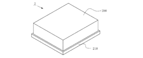
- FIG. 6 is a perspective view of the light receiving element according to the embodiment.
- FIG. 7 is a top view of the light receiving element according to the embodiment.
- FIG. 8 is a perspective view of the light emitting device according to the second embodiment.
- FIG. 9 is a perspective view of the light emitting device according to the second embodiment excluding the lid member.
- polygons such as triangles and quadrangles are referred to as polygons, including shapes in which the corners of the polygon are rounded, chamfered, chamfered, rounded, etc. It shall be called. Further, not only the corner (edge of the side) but also the shape in which the middle part of the side is processed is also referred to as a polygon. That is, the partially processed shape while leaving the polygon as the base is included in the interpretation of the "polygon" described in the present specification and the claims.
- FIG. 1 is a perspective view of the light emitting device 1.
- FIG. 2 is a perspective view showing a state in which the lid member 80 is removed from the light emitting device 1.
- FIG. 3 is a top view of a state similar to that of FIG.
- FIG. 4 is an enlarged view of a portion X of the light receiving surface 42 of the light receiving element 40 in the top view of FIG.
- FIG. 5 is a cross-sectional view taken along the VV cross-sectional line of FIG.
- FIG. 6 is a perspective view of the light receiving element 40.
- FIG. 7 is a top view of the light receiving element 40.
- the wiring region 14 provided in the stepped portion 13 of the base portion 10 is shown by hatching.
- the broken line indicating the part X is a virtual line.
- the elliptical region indicated by the dotted line on the light receiving surface 42 indicates the region to be irradiated with light.
- an example of the third central region 463 is shown by hatching having a large width, and the end region 47 based on the third central region 463 is shown by hatching having a small width.
- the third central region 463 and the alternate long and short dash line drawn to indicate the width Y are virtual lines. Further, in FIG.
- the second central region 462 is shown by hatching having a large width
- the end region 47 based on the second central region 462 is shown by hatching having a small width.
- the first central region 461, the second central region 462, the width S, the width T, and the alternate long and short dash line drawn to indicate the middle line P are virtual lines.
- the light emitting device 1 has a plurality of components including a base 10, a semiconductor laser element 20, a submount 30, a light receiving element 40, a support base 50, a protection element 60, a plurality of wirings 70, and a lid member 80 (support base). For 50, see FIG. 5 in particular).
- three semiconductor laser elements 20, a submount 30, a light receiving element 40, a support base 50, and a plurality of wirings 70 are provided in a space surrounded by a base 10 and a lid member 80. Have been placed. Further, the light emitted from the three semiconductor laser elements 20 arranged in the space is emitted to the outside of the light emitting device 1.
- the base 10 has an arrangement area, which is an area where other components are arranged, and a side wall surrounding the arrangement area. Further, the base portion 10 has a recess, and the recess is formed by an arrangement area and a side wall. The recess is recessed from the upper surface of the base 10 toward the lower surface. Here, the surface that becomes the bottom of the recess is called the bottom surface. The bottom surface can be a major part of the placement area.
- the outer shape of the base 10 is rectangular. Further, when viewed from above, the outer shape of the recessed portion is rectangular. Further, when viewed from above, the outer shape of the bottom surface of the base 10 is rectangular. The outer shape of the bottom surface is smaller than the outer shape of the recessed part. It should be noted that none of these outer shapes need be rectangular.
- the base portion 10 has a bottom surface portion 11 and a side surface portion 12.
- the bottom surface portion 11 is a portion constituting the bottom surface of the base portion 10. Further, the bottom surface portion 11 includes a bottom surface of the base portion 10 and a bottom surface.
- the side surface portion 12 is a portion constituting the side wall of the base portion 10. Therefore, the side surface portion 12 surrounds the bottom surface of the base portion 10 and extends upward from the bottom surface.
- the side surface portion 12 includes one or more outer surfaces of the base portion 10, one or more inner surfaces, and an upper surface that intersects the outer surface and the inner surface.
- the number of surfaces on the inner surface or the outer surface of the base 10 depends on the shape surrounding the bottom surface.
- the shape surrounding the bottom surface is rectangular, inner side surfaces corresponding to each of the four sides of the rectangle are formed, and the number of surfaces on the inner side surface is plural.
- the shape surrounding the bottom surface is circular, an inner surface corresponding to one circle is formed, and the number of surfaces on the inner surface is one. The same applies to the outer surface.
- the base 10 has one or more stepped portions 13.
- the step portion 13 is formed in a recessed portion of the base portion 10.
- the step portion 13 refers to a portion composed of only an upper surface and an inner side surface that intersects the upper surface and extends downward.
- the step portion 13 is included in the side surface portion 12 of the base portion 10. Further, the step portion 13 is provided below the upper surface of the base portion 10. Further, in top view, it is formed between the outer shape of the recessed portion of the base 10 and the outer shape of the bottom surface.
- the step portion 13 is formed along the inner side surface that intersects the upper surface of the base portion 10. Therefore, the inner side surface that intersects the upper surface of the base portion 10 and the upper surface of the step portion 13 intersect. Further, the step portion 13 is formed along a part of the inner side surface that intersects the upper surface of the base portion 10. In other words, the step portion 13 is not provided along the entire circumference of the inner side surface that intersects the upper surface of the base portion 10. In addition, it may be provided along the entire circumference.
- the outer shape of the inner side surface intersecting the upper surface of the base portion 10 is rectangular in top view, and the step portion 13 is provided over three sides of this rectangle. Further, one side of the rectangle is not provided with the step portion 13 except for the intersection with the other side. The number of sides along which the step portion 13 is along does not have to be three.
- the step portion 13 is preferably provided along 50% or more of the entire circumference of the inner surface surface intersecting the upper surface of the base portion 10. As a result, it is possible to secure a sufficient area for providing the wiring area in the step portion 13. Further, it is preferably 90% or less.
- the step portion 13 is not provided in the region unsuitable for providing the wiring region, and the base portion 10 can be designed to be compact. In addition, it may be provided along the entire circumference.
- One or more wiring regions 14 are provided on the upper surface of the step portion 13.
- a plurality of wiring regions 14 are provided.
- the wiring region 14 passes through the inside of the base portion 10 and is electrically connected to the wiring region provided on the lower surface of the base portion 10.
- the wiring region electrically connected to the wiring region 14 is not limited to the lower surface of the base portion 10, but can be provided on the outer surface (upper surface, outer surface, and lower surface) of the base portion 10.
- the base 10 can be formed using ceramic as the main material.
- the ceramic used for the base 10 include aluminum nitride, silicon nitride, aluminum oxide, and silicon carbide.
- the base portion 10 can be formed by integrally forming the bottom surface portion 11 and the side surface portion 12. Further, the bottom surface portion 11 and the side surface portion 12 which are separately formed by using different materials as the main materials may be joined and formed. In this case, for example, the bottom surface portion 11 may be made of metal and the side surface portion 12 may be made of ceramic as the main material.
- the metal used for the bottom surface portion 11 is preferably one having better heat dissipation (high thermal conductivity) than the ceramic used for the side surface portion 12.
- the ceramic used for the side surface portion 12 For example, copper, aluminum, iron and the like, or as a composite, copper molybdenum, copper-diamond composite material, copper tungsten and the like can be used.
- a metal film is provided at each of the wiring region 14 of the base portion 10 and the portion corresponding to the wiring region electrically connected to the wiring region 14. Further, for electrical connection, metal is also provided at a place passing through the inside, whereby electrical connection is achieved.
- the semiconductor laser device 20 has a rectangular outer shape when viewed from above. Further, the side surface that intersects with one of the two short sides of the rectangle is the emission end surface of the light emitted from the semiconductor laser element 20. Further, the upper surface and the lower surface of the semiconductor laser element 20 have a larger area than the emission end surface.
- the semiconductor laser device 20 is a multi-emitter having two or more emitters. A single emitter having one emitter may be used. In the illustrated example of the light emitting device 1, the semiconductor laser device 20 has two emitters. Further, one electrode common to the two emitters is provided on one of the upper surface and the lower surface of the semiconductor laser element 20, and two electrodes corresponding to the respective emitters are provided on the other side.
- the light (laser light) emitted from each emitter of the semiconductor laser element 20 has a spread and forms an elliptical farfield pattern (hereinafter referred to as "FFP") on a surface parallel to the emission end surface of the light.
- FFP is the shape and light intensity distribution of emitted light at a position away from the emitted end face.
- the light passing through the center of the elliptical shape of the FFP in other words, the light having the peak intensity in the light intensity distribution of the FFP is referred to as the light traveling on the optical axis.
- the light having an intensity of 1 / e 2 or more with respect to the peak intensity value is referred to as the light of the main portion.
- the shape of the FFP of the light emitted from the semiconductor laser element 20 is an elliptical shape in which the stacking direction perpendicular to the layer direction of the plurality of semiconductor layers including the active layer is longer than the layer direction.
- the layer direction is the horizontal direction of FFP
- the stacking direction is the vertical direction of FFP.
- the angle corresponding to the full width at half maximum of the light intensity distribution is defined as the light spread angle of the semiconductor laser device.
- the spread angle of light in the vertical direction of the FFP is defined as the spread angle in the vertical direction
- the spread angle of light in the horizontal direction of the FFP is referred to as the spread angle in the horizontal direction.
- the semiconductor laser element 20 for example, a semiconductor laser element that emits blue light, a semiconductor laser element that emits green light, a semiconductor laser element that emits red light, or the like can be adopted. Further, a semiconductor laser device that emits light other than these may be adopted.
- blue light refers to light whose emission peak wavelength is in the range of 420 nm to 494 nm.
- the green light refers to light whose emission peak wavelength is in the range of 495 nm to 570 nm.
- the red light refers to light whose emission peak wavelength is in the range of 605 nm to 750 nm.
- Examples of the semiconductor laser device that emits blue light or the semiconductor laser device that emits green light include a semiconductor laser device containing a nitride semiconductor.
- a semiconductor laser device containing a nitride semiconductor for example, GaN, InGaN, and AlGaN can be used.
- Examples of the semiconductor laser device that emits red light include those including InAlGaP-based, GaInP-based, GaAs-based, and AlGaAs-based semiconductors.
- the submount 30 has two joint surfaces and is composed of a rectangular parallelepiped shape. Further, the other joint surface is provided on the opposite side of one joint surface. Also, the distance between the two joint surfaces is smaller than the distance between the other two opposing surfaces.
- the shape of the submount 30 does not have to be limited to a rectangular parallelepiped.
- the submount 30 can be formed using, for example, silicon nitride, aluminum nitride, or silicon carbide. Further, a metal film for joining is provided on the joining surface.
- the light receiving element 40 has a joint surface 41 and a light receiving surface 42.
- the joint surface 41 is a surface opposite to the light receiving surface 42. It does not have to be on the opposite side.
- the light receiving element 40 has an upper surface, a lower surface, and one or more side surfaces.
- the surface having the light receiving surface 42 is the upper surface.
- the outer shape of the light receiving element 40 is a rectangular parallelepiped, but the outer shape is not limited to the rectangular parallelepiped.
- a plurality of light receiving regions 43 are provided on the light receiving surface 42.
- three light receiving regions 43 are provided.
- the number of light receiving regions 43 is not limited to three.
- the plurality of light receiving regions 43 are arranged side by side at predetermined intervals.
- the direction in which the plurality of light receiving regions 43 are lined up is referred to as the first direction.
- the arrow direction of 1D in FIG. 7 indicates a first direction based on the example of the light receiving element 40 shown.
- the light receiving surface 42 has a rectangular outer shape. Further, the length of the light receiving surface 42 in the first direction is larger than the length in the second direction.
- the second direction is a direction perpendicular to the first direction in a top view.
- the 2D arrow direction in FIG. 7 indicates a second direction based on the example of the light receiving element 40 shown.
- the length in the first direction and the length in the second direction may be the same. Further, the length in the second direction may be larger than the length in the first direction.
- the plurality of light receiving regions 43 are close to each other and lined up at regular intervals. That is, the light receiving regions 43 are separated and do not overlap. The interval does not have to be constant.
- the distance between the adjacent light receiving regions 43 is smaller than the width in the first direction in any one of the adjacent light receiving regions 43. As a result, the intervals of the light radiated to each light receiving region 43 can be brought close to each other.
- Each light receiving region 43 is formed on the light receiving surface 42 with a rectangular outer shape. It should be noted that the design is not limited to a rectangle, and may be appropriately designed according to the shape of the emitted light. In the illustrated light receiving element 40 example, each light receiving region 43 is formed with a rectangular outer shape. The two sides (short sides in the case of a rectangle) of one of the two opposing sides forming a rectangle are parallel to the first direction. The parallelism here includes an error within ⁇ 5 degrees.
- the length of the light receiving region 43 in the second direction is larger than the length in the first direction. In the illustrated example of the light emitting device 1, all the light receiving regions 43 satisfy this condition.
- the light receiving region 43 having the same length in the first direction and the second direction may be included. Further, the light receiving region 43 whose length in the first direction is larger than the length in the second direction may be included.
- the plurality of light receiving regions 43 include two light receiving regions 43 having different lengths in the second direction on the light receiving surface 42. Further, at least one of the light receiving regions 43 arranged at both ends has a smaller length in the second direction on the light receiving surface 42 than the light receiving region 43 arranged next to the light receiving region 43. Further, the lengths of the light receiving regions 43 arranged at both ends in the second direction are different.
- the light receiving element 40 can be miniaturized.
- the light receiving element 40 In the example of the light receiving element 40 shown in the figure, three light receiving regions 43 are arranged side by side in the first direction. Further, the light receiving region 43 arranged at one end of both ends has a shorter length in the second direction than the other light receiving region 43.
- the light receiving element 40 is downsized by providing a conduction region 45, which will be described later, in the space created by the difference in length.
- the lengths of all the light receiving regions 43 in the second direction may be the same. Further, all of the light receiving regions 43 arranged at both ends may have a smaller length in the second direction on the light receiving surface 42 than the light receiving regions 43 arranged next to the light receiving regions 43. Further, the lengths of the light receiving regions 43 arranged at both ends in the second direction may be the same.
- the plurality of light receiving regions 43 are arranged so that one end of either end of the light receiving region 43 in the second direction is aligned.
- the straight line connecting the end points of any one of both ends in the second direction in each light receiving region 43 is parallel to the first direction.
- the parallelism here includes a difference within ⁇ 5 degrees.
- the plurality of light receiving areas 43 include two light receiving areas 43 arranged adjacent to each other. Further, the plurality of light receiving regions 43 include two light receiving regions 43 arranged at both ends. Further, the plurality of light receiving regions 43 include two light receiving regions 43 having different lengths in the second direction. Further, the plurality of light receiving regions 43 may be all the light receiving regions 43. By aligning the positions of one end, it is possible to contribute to the miniaturization of the light receiving element 40.
- the light receiving element 40 When the light receiving element 40 has two light receiving regions 43 having different lengths in the second direction, by aligning one end, the other end is not aligned. At this time, the distance between the other end in one light receiving region 43 and the other end in the other light receiving region 43 in the second direction is the same as the difference in length between the two light receiving regions 43 in the second direction. ..
- a plurality of light receiving regions 43 in which neither end of the second direction is aligned in other words, a plurality of straight lines connecting the ends of the plurality of light receiving regions 43 in any of both ends are not parallel to the first direction. It may have a light receiving region 43 of.
- the light receiving region 43 having the shorter length in the second direction Is provided between a straight line passing through one end point of both ends in the second direction of the longer light receiving region 43 and parallel to the first direction and a straight line passing through the other end point and parallel to the first direction. Is preferable in designing the light receiving element 40 to be compact.
- a plurality of wiring regions 44 are provided on the light receiving surface 42 of the light receiving element 40.
- the number of wiring areas 44 may be 1 or more. Further, the wiring region may be provided not only on the light receiving surface 42 but also on a surface other than the light receiving surface 42. Each wiring area is electrically connected to the light receiving area 43.
- the light receiving surface 42 is provided with a plurality of wiring areas 44 that are electrically connected to the plurality of light receiving areas 43.
- the plurality of light receiving regions 43 include two light receiving regions 43 arranged adjacent to each other.
- the plurality of light receiving regions 43 include two light receiving regions 43 arranged at both ends.
- the plurality of light receiving regions 43 include two light receiving regions 43 having different lengths in the second direction.
- the plurality of light receiving regions 43 include all the light receiving regions 43 provided on the light receiving surface 42.
- a plurality of wiring regions 44 that are electrically connected to all the light receiving regions 43 arranged on the light receiving surface 42 are provided. Specifically, there are four wiring regions 44 that are electrically connected to the three light receiving regions 43. That is, the light receiving surface 42 is provided with more wiring regions 44 than the number of light receiving regions 43.
- Three of the four wiring regions 44 are electrically connected to the anode electrode of any of the three light receiving regions 43 without overlapping each other. The remaining one is electrically connected to a cathode electrode common to the three light receiving regions 43.
- the plurality of wiring regions 44 are provided in the end regions 47 on the light receiving surface 42 (shown in FIG. 7).
- the end region 47 is a region on the light receiving surface 42 excluding the central region 46.
- the first central region 461 is a straight line extending in the second direction through the midpoint of the width in the first direction in the light receiving region 43 arranged at one end of the light receiving regions 43 arranged at both ends on the light receiving surface 42. It is a region sandwiched between the light receiving region 43 arranged at the other end and a straight line extending in the second direction through the midpoint of the width in the first direction.
- the second central region 462 refers to the end point of the light receiving surface 42 located at the farthest position from the light receiving region 43 at the other end of the light receiving region 43 arranged at one end of the light receiving regions 43 arranged at both ends. It is a region sandwiched between a straight line extending in the second direction and a straight line extending in the second direction through the end point located at the farthest position from the light receiving region 43 at one end in the light receiving region 43 arranged at the other end. ..
- the first central region 461 is included in the second central region 462. Therefore, the end region 47 when the second central region 462 is the central region 46 is included in the end region 47 when the first central region 461 is the central region 46.
- the central region 46 may be a region including at least the first central region 461 or the second central region 462.
- the central region 46 here may be either the first central region 461 or the second central region 462.
- the central region 46 here may be either the first central region 461 or the second central region 462.
- the plurality of wiring regions 44 that are electrically connected to the two light receiving regions 43 having different lengths in the second direction are provided in the end region 47. Further, it is not provided in the central region 46.
- the central region 46 here may be either the first central region 461 or the second central region 462.
- the central region 46 may be either the first central region 461 or the second central region 462.
- the end region 47 is divided into two regions separated by sandwiching the central region 46.
- One region separated by the central region 46 is referred to as the first portion of the end region 47, and the other region is referred to as the second portion of the end region 47.
- One or more wiring regions 44 are provided in the first portion of the end region 47, and one or more wiring regions 44 are provided in the second portion of the end region 47.
- the wiring areas 44 By providing the wiring areas 44 on both sides, the wiring is not concentrated on one side portion, so that the distance between the wirings can be widened and the wiring becomes easy. It should be noted that a plurality of wiring areas 44 may be provided in either one of the first portion and the second portion, and the wiring area 44 may not be provided in the other portion.
- the number of wiring regions 44 provided in the first portion of the end region 47 and the number of wiring regions 44 provided in the second portion of the end region 47 are the same or one difference. By equalizing the number of the wiring areas 44 provided in this way, the distance between the wirings can be widened, and the wiring becomes easy.
- two wiring regions 44 are provided in each of the first portion and the second portion of the end region 47.
- the light receiving element 40 is provided with a plurality of conduction regions 45 on the light receiving surface 42.
- the conduction region 45 may be one, or the conduction region 45 may not be present.
- the conduction region 45 connects the light receiving region 43 and the wiring region 44. As a result, the light receiving region 43 and the wiring region 44 are electrically connected.
- the wiring region 44 and the conduction area 45 will be described.
- the wiring region 44 and the conduction region 45 may be provided with different materials, or may be provided with the same material. When provided with the same material, there may be no apparent boundary between the wiring region 44 and the conduction region 45. In such a case, the wiring area 44 may be defined as follows to specify the boundary between the wiring area 44 and the conduction area 45.
- the plurality of wiring areas 44 are areas to which the wirings for electrically connecting the light receiving areas 43 are joined.
- the bonding device specifies a position where the wiring region 44 is provided and joins the wiring. Therefore, the wiring area 44 can be defined as an area in which the wiring is actually joined based on the relationship of the connection with the wiring.
- the wiring region 44 is provided with a predetermined shape as a target of the wiring joint position.
- the wiring region 44 is defined as an region having the same shape and size as the outer shape, which is common among a plurality of regions provided on the light receiving surface 42 for electrically connecting the light receiving region 43. be able to.
- the illustrated light receiving element 40 has four regions as a plurality of regions provided on the light receiving surface 42 for electrically connecting the light receiving region 43. Further, one of them is a wiring region 44 that is electrically connected to the cathode electrode of the light receiving region 43. The remaining three are regions in which the wiring regions 44 and the conduction regions 45, which are electrically connected to the anode electrodes of the light receiving region 43, are connected to each other. Further, each light receiving region 44 is a region having a rectangular shape and size having the same outer shape.
- the shape of the area provided as the target of the wiring joint position does not have to be the same. Even in this case, it is necessary to secure the minimum area that must be secured for wiring connection. Therefore, when there is no commonality in the outer shapes, when each of the plurality of regions provided on the light receiving surface 42 for electrically connecting the light receiving region 43 is overlapped, the maximum range that overlaps in all the regions is set. It can be defined as the wiring area 44. In the example of the light receiving element 40 shown in the figure, the maximum range in which all four regions can be overlapped is the wiring region 44.
- a region excluding the wiring region 44 from the region provided on the light receiving surface 42 for electrically connecting the light receiving region 43 can be defined as the conduction region 45. it can.
- the boundary between the wiring area 44 and the conduction area 45 is not limited to the method described here. It may be determined by a method that can be reasonably interpreted, such as when it can be clearly distinguished from the viewpoint of appearance and material, or when it can be clearly distinguished from the manufacturing process of the light receiving element 40.
- each conducting region 45 in the second direction is shorter than the length of the light receiving region 43 in the second direction. Further, it is shorter than the length of the wiring region 44 in the second direction. Further, the plurality of conduction regions 45 include a conduction region 45 whose length in the first direction is longer than the length in the first direction of one light receiving region 43. Further, the plurality of conduction regions 45 include a conduction region 45 whose length in the first direction is shorter than the length in the first direction of one light receiving region 43.
- the light receiving surface 42 is provided with a plurality of conduction regions 45 connecting the plurality of light receiving regions 43 and the plurality of wiring regions 44. Further, the plurality of light receiving regions 43 include two light receiving regions 43 arranged adjacent to each other. Further, the plurality of light receiving regions 43 include two light receiving regions 43 arranged at both ends. Further, the plurality of light receiving regions 43 include two light receiving regions 43 having different lengths in the second direction.
- the plurality of light receiving regions 43 include all the light receiving regions 43 provided on the light receiving surface 42. Further, the plurality of wiring areas 44 do not include one or more wiring areas 44 among all the wiring areas 44 provided on the light receiving surface 42. It should be noted that the entire wiring region 44 provided on the light receiving surface 42 may be included.
- a plurality of conduction regions 45 connected to each of all the light receiving regions 43 arranged on the light receiving surface 42 are provided. Specifically, there are three conduction regions 45 connected to the three light receiving regions 43. That is, the number of light receiving regions 43 arranged on the light receiving surface 42 and the number of conductive regions 45 are equal.
- the conduction region 45 connects the light receiving region 43 and the wiring region 44 that is electrically connected to the anode electrode of the light receiving region 43.
- the wiring region 44 that is electrically connected to the cathode electrode of the light receiving region 43 is not connected to the conduction region 45.
- the wiring region 44 is electrically connected to the cathode electrode of the light receiving region 43 inside the light receiving element 40.
- the number of conduction regions 45 provided on the light receiving surface 42 can be reduced, which contributes to the compact design of the light receiving element 40. Can be done. It may have a conduction region 45 connecting the cathode electrode of the light receiving region 43 and the wiring region 44.
- the plurality of conduction regions 45 include a conduction region 45 provided from the central region 46 to the end region 47. Further, the plurality of conduction regions 45 include a conduction region 45 provided in the end region 47 and not provided in the central region 46.
- the central region 46 here may be either the first central region 461 or the second central region 462.
- the plurality of conduction regions 45 are connected to one of the two light receiving regions 43 arranged adjacent to each other, and are provided from the central region 46 to the end region 47, and the other of the conduction regions 45. It includes a conduction region 45 that is connected to the light receiving region 43 and is not provided in the central region 46 but is provided in the end region 47.
- the other light receiving region 43 is a light receiving region 43 arranged at the end of a plurality of light receiving regions 43 arranged side by side in the first direction.
- the conductive region 45 provided from the central region 46 to the end region 47 and the end region 47 not provided in the central region 46.
- the conductive region 45 provided extends from a position connected to the light receiving region 43 in the first direction and is connected to the wiring region 44.
- Each of the wiring regions 44 is provided in the first portion and the second portion of the end region 47, whichever is closer to the light receiving region 43 arranged at the end.
- the conduction region 45 provided from the central region 46 to the end region 47 is connected to the side of one of the two opposing sides of the two light receiving regions 43 arranged adjacent to each other. Further, it extends from the position connected to this side in the first direction in parallel with the first direction and is connected to the wiring area 44.
- the light receiving element 40 is connected to a straight line parallel to the second direction through one end connected to the light receiving region 43 and a wiring region 44 among both ends of the conductive region 45 provided from the central region 46 to the end region 47. It has a light receiving region 43 sandwiched between a straight line passing through the end and parallel to the second direction.
- the light receiving region 43 having the shorter length in the second direction is provided in the range of the width S shown in the figure.
- the conduction region 45 which is electrically connected to one of the two light receiving regions 43 arranged adjacent to each other and is provided from the central region 46 to the end region 47, is different from the other light receiving region 43. Do not connect electrically.
- a method of avoiding electrical connection there is a method of providing an insulating region in a part of the other light receiving region 43 and providing a conductive region 45 on the insulating region. Since the insulating region is provided on the light receiving region 43, the position where the insulating region is provided can be adjusted.
- the conduction region 45 is connected to the one light receiving region 43 at a portion protruding from the other light receiving region 43 in the second direction, and extends in a direction parallel to the first direction. It connects to the wiring area 44.
- the conduction region 45 which is not provided in the central region 46 but is provided in the end region 47, is an adjacent light receiving region 43 in the light receiving region 43 arranged at the end of the two light receiving regions 43 arranged adjacent to each other. It connects to the side opposite to the side facing.
- the conduction region 45 provided from the central region 46 to the end region 47 is connected to the light receiving region 43 near the upper end or the lower end of the light receiving region 43. This is because the closer to the end, the more the other light receiving region 43 can be suppressed from being reduced, and a wider light receiving region can be secured.
- the wiring region 44 is a straight line extending in the first direction through one end of both ends at the most end in the second direction among the plurality of light receiving regions 43, and the first direction passing through the other end. It is preferable that it is provided in a region sandwiched between a straight line extending in. It is possible to prevent the light receiving element 40 from becoming large in the second direction. In the example of FIG. 7, all the wiring regions 44 are within the range of the width T shown in the figure. The same can be said even if the wiring region 44 is replaced with the conduction region 45.
- the wiring region 44 is provided not near the center of the light receiving surface 42 but near one end of the light receiving surface 42 in the second direction.
- both the wiring region 44 closest to one end of both ends at the end in the second direction and the wiring region 44 closest to the other end are the other. It is preferably located closer to one end than the end. Further, it is preferable that the same can be said even if the plurality of light receiving regions 43 are replaced with the light receiving surfaces 42.
- the wiring region 44 located closest to one end of both ends which is the farthest end in the second direction among the plurality of light receiving regions 43, is provided at a position closer to this one end than the center of both ends. Moreover, it is preferable that the wiring region 44 closest to the other end is provided at a position closer to the center of both ends than the other end. Further, it is preferable that the same can be said even if the plurality of light receiving regions 43 are replaced with the light receiving surfaces 42.
- the virtual line P shown in the figure shows the center lines of both ends at the most end in the second direction among the plurality of light receiving regions 43.
- the virtual line P indicates the center line of the light receiving surface 42.
- one of the two wiring regions 44 in the first portion of the end region 47 becomes the wiring region 44 closest to one end at both ends, and the other is the position closest to the other end at both ends. It becomes the wiring area 44 in, and satisfies these. The same can be said if the first part is replaced with the second part.
- the light receiving element 40 for example, a photodiode (hereinafter, PD, which is abbreviated as abbreviation) can be adopted. Further, the light receiving element 40 reflects 80% or more of the light irradiated to the light receiving region 43.
- PD photodiode
- the support base 50 has a lower surface and an inclined surface 51 inclined with respect to the lower surface.
- the inclined surface 51 is neither vertical nor parallel when viewed from the lower surface.
- the inclined surface 51 is composed of a plane having an inclination angle of 40 degrees or more and 50 degrees or less with respect to the lower surface.
- the inclined surface 51 is formed of a plane having an inclination angle of 45 degrees with respect to the lower surface.
- the inclined surface 51 may be formed in a range where the inclination angle is 10 degrees or more and 80 degrees or less.
- the inclined surface 51 is one or a plurality of inclined surfaces that are inclined with respect to the lower surface of the support base 50, and is the inclined surface having the largest area when there are a plurality of inclined surfaces. Further, the inclined surface 51 occupies an area of 60% or more of the support base 50 when viewed from above. Further, when viewed from above, the width from the upper end to the lower end of the inclined surface 51 is 60% or more of the width of the support base 50 in the same direction. That is, the support base 50 is mainly occupied by the inclined surface 51.
- the support base 50 can be formed by using, for example, ceramic, glass, metal, or the like.
- ceramics such as aluminum nitride, glass such as quartz or borosilicate glass, and metals such as aluminum can be used. Alternatively, it can also be formed using Si or the like.
- the protective element 60 is for preventing an excessive current from flowing to a specific element (for example, the semiconductor laser element 20) and destroying the element.
- Examples of the protection element 60 include a Zener diode. Further, as the Zener diode, a diode made of Si can be adopted.
- the wiring 70 has a linear shape with both ends as joints. That is, it has joints at both ends of the linear portion to join with other components.
- the wiring 70 is, for example, a metal wire.
- the metal for example, gold, aluminum, silver, copper and the like can be used.
- the lid member 80 has a lower surface and an upper surface, and is formed of a rectangular parallelepiped flat plate shape. It does not have to be a rectangular parallelepiped. Further, the lid member 80 has a translucent property that transmits light. Here, the translucency means that the transmittance with respect to light is 80% or more. It is not necessary to have a transmittance of 80% or more for light of all wavelengths. Further, the lid member 80 may have a non-translucent region (a region having no translucency) in a part thereof.
- the lid member 80 can be formed using sapphire.
- Sapphire is a material that has translucency, has a relatively high refractive index, and has a relatively high strength.
- glass or the like can also be used.
- the light emitting device 1 includes a base 10, a semiconductor laser element 20 arranged on the base 10, a light receiving element 40 arranged on the base 10, and a plurality of semiconductor laser elements 20 among a plurality of wirings 70 for electrically connecting. It has a first wiring 71 and a plurality of second wirings 72 for electrically connecting the light receiving element 40 of the plurality of wirings 70.
- the semiconductor laser element 20 another light emitting element such as an LED may be used.
- the semiconductor laser element 20 is arranged on the base 10 via the submount 30. In addition, it may be arranged directly on the bottom surface of the base portion 10 without passing through the sub mount 30. When the submount 30 is not used, the outer shape of the semiconductor laser element 20 may be changed in order to adjust the light emission position (height) on the emission end face.
- the light receiving element 40 is arranged on the base 10 via the support base 50. It should be noted that it may be arranged directly on the bottom surface of the base 10 without going through the support base 50. If the support base 50 is not used, the outer shape of the light receiving element 40 may be changed in order to adjust the position (height) and orientation (tilt) of the light receiving surface 42.
- the light emitting device 1 is arranged at the base 10 and has a protective element 60 that protects the semiconductor laser element 20. Further, the light emitting device 1 has a lid member 80 that is joined to the base portion 10 and seals the space in which the semiconductor laser element 20 is arranged.
- the semiconductor laser element 20 is arranged on the bottom surface (arrangement region) of the base 10. Further, a plurality of semiconductor laser elements 20 may be arranged. Further, the plurality of semiconductor laser elements 20 are arranged side by side so that the emission end faces face the same direction. Further, between the adjacent semiconductor laser elements 20, the side surfaces that intersect with the respective emission end faces face each other.
- the direction in which the plurality of semiconductor laser elements 20 are lined up in the top view is referred to as the first direction.
- the direction perpendicular to the first direction in the top view is referred to as the second direction.
- the first direction and the second direction based on the example of the illustrated light emitting device 1 are shown by 1D and 2D in FIG. 3, respectively.
- the direction in which the plurality of emitters are lined up may be referred to as the first direction.
- the first direction is parallel to the emission end surface of the semiconductor laser element 20 in a top view.
- the side surfaces that intersect with each emission end surface and face each other between the adjacent semiconductor laser elements 20 are parallel in top view.
- the three semiconductor laser elements 20 are composed of a semiconductor laser element that emits blue light, a semiconductor laser element that emits green light, and a semiconductor laser element that emits red light.
- the configuration is not limited to this, and a configuration having a plurality of semiconductor laser elements that emit light of the same color may be used, or a configuration having semiconductor laser elements that emit light of other colors may be used.
- the submount 30 is bonded to the semiconductor laser element 20 at one of the bonding surfaces. Further, the other joint surface on the opposite side is joined to the bottom surface of the base portion 10.
- the light emitting device 1 may have a plurality of submounts 30. The number of semiconductor laser elements 20 arranged in one submount 30 may be one.
- the light receiving element 40 is arranged on the bottom surface of the base 10. Further, the light receiving surface 42 is arranged in the direction in which the light emitted from the semiconductor laser element 20 is irradiated. Further, the plurality of light receiving regions 43 of the light receiving surface 42 are irradiated with the light of the main portion emitted from the semiconductor laser element 20. Further, one light receiving region 43 is irradiated with light of a main portion of at least one laser beam. That is, the light of the main part of the two laser beams may be irradiated.
- the plurality of light receiving regions 43 provided on the light receiving surface 42 of the light receiving element 40 are irradiated with the light emitted from the plurality of semiconductor laser elements 20. Further, one light receiving region 43 corresponds to one semiconductor laser element 20, and one light receiving region 43 is irradiated with light of a main portion emitted from one semiconductor laser element 20.
- the three light receiving regions 43 are irradiated with the light of at least the main part of the light emitted from the three semiconductor laser elements 20. Further, one light receiving region 43 is irradiated with two laser beams emitted from each of the two emitters of one semiconductor laser element 20.
- the light receiving element 40 receives (absorbs) a part of the light radiated to the light receiving region 43 and reflects a part of the light.
- the light receiving region 43 receives 2% or more of the light of the irradiated main portion. Further, the light receiving region 43 reflects 80% or more of the light of the irradiated main portion. The sum of the received light and the reflected light is 100% or less.
- first direction in the light emitting device 1 and the first direction in the light receiving element 40 are the same direction and are parallel. Further, in top view, the emission end surface of the semiconductor laser element 20 and the lower end side or the upper end side of the light receiving surface 42 of the light receiving element 40 are parallel to each other. Parallelism here includes a difference of up to 5 degrees. It does not have to be parallel.
- the light receiving region 43 reflects the light emitted laterally from the semiconductor laser element 20 upward. Therefore, the light receiving surface 42 is tilted with respect to the emission end surface and the optical axis. It also tilts with respect to the bottom surface of the base 10.
- the light receiving surface 42 is tilted at an angle of 40 degrees or more and 50 degrees or less with respect to the traveling direction of light passing through the optical axis. In the illustrated example of the light emitting device 1, it is tilted at an angle of 45 degrees. It may be tilted at an angle in the range of 10 degrees or more and 80 degrees or less.
- the wiring region 44 of the light receiving element 40 is arranged at a position where it does not enter the optical path of the light of the main portion emitted from the semiconductor laser element 20. Further, the second wiring 72 joined to the wiring region 44 is arranged at a position where it does not enter the light path of the main portion.
- the end region 47 here is an region excluding the central region 46, and a third central region 463 is defined as the central region 46 here.
- the third central region 463 is a top view of the light passing through the optical axis of the light radiating to the light receiving region 43 arranged at one end of the light receiving regions 43 arranged at both ends on the light receiving surface 42. It is sandwiched between a straight line extending in the second direction through the irradiation point and a straight line extending in the second direction through the irradiation point of the light passing through the optical axis among the light emitted to the light receiving region 43 arranged at the other end.
- the area It may be at least a region including this region.
- the provision of the third central region 463 may be satisfied based on at least one of the laser beams. Further, it is preferable that the provision of the third central region 463 is satisfied based on the laser beam radiated to both ends in the first direction. In the example of FIG. 4, the third central region 463 based on the laser beam radiated to both ends is shown by hatching.
- the plurality of light receiving regions 43 in the light receiving element 40 include two light receiving regions 43 having different lengths in the second direction, the spread angles of the plurality of laser beams emitted from the semiconductor laser element 20 in the vertical direction are increased. Therefore, the light receiving region 43 to be irradiated with the laser beam may be determined. This is because the laser beam having a large spread angle in the vertical direction forms a longer irradiation region in the second direction in the light receiving region 43.
- the light of the main portion of the laser beam having the largest vertical light spread angle among the plurality of laser beams irradiates the longer light receiving region 43 of the two light receiving regions 43 having different lengths in the second direction. It is good to be done. In other words, the light of the main portion of the laser beam having the largest vertical light spread angle among the plurality of laser beams is in the shorter light receiving region of the two light receiving regions 43 having different lengths in the second direction. Is preferably not irradiated.
- the light receiving region 43 arranged at one end of the light receiving regions 43 arranged at both ends of the plurality of light receiving regions 43 arranged in the first direction is in the second direction.
- the length is smaller than the length of the light receiving region 43 arranged next to the light receiving region 43 in the second direction.
- the light of the main portion emitted from the semiconductor laser element 20 having the largest vertical light spread angle among the plurality of semiconductor laser elements 20 is the light receiving region 43 arranged at one end of both ends and is adjacent to the light receiving region 43.
- the light receiving region 43 having a length smaller than that of the light receiving region 43 arranged in the second direction is not irradiated, and the other light receiving region 43 having a length in the second direction larger than this light receiving region 43 is irradiated.
- the semiconductor laser element 20 and the light receiving element 40 are arranged.
- the light of the main portion emitted from the semiconductor laser element 20 that emits red light having the largest vertical light spread angle is in the second direction of both ends.
- the light receiving region 43 at the end having the larger length is irradiated.
- the light receiving region 43 sandwiched between both ends is also the light receiving region 43 having a larger length in the second direction, but it is preferable to arrange the semiconductor laser element 20 which is more susceptible to heat than the others at the end. ..
- the semiconductor laser device 20 that emits red light is more affected by heat than the semiconductor laser device 20 that emits blue light and the semiconductor laser device 20 that emits green light. It has easy light emission characteristics.
- the conduction region 45 provided from the first central region 461 or the second central region 462 to the end region 47 is provided from the third central region 463 to the end region 47.
- the conduction region 45 provided from the central region 46 to the end region 47 is provided near the upper end of the light receiving region 43 arranged at the end of the light emitting device 1.
- the conduction region 45 is also arranged at a position where it does not enter the optical path of the light of the main portion emitted from the semiconductor laser element 20.
- the conduction region 45 provided from the central region 46 to the end region 47 extends in the first direction on the light receiving surface 42 through the upper end of the light receiving region 43 arranged next to the light receiving region 43 arranged at the end. It is provided below the straight line and above the upper end of the light of the main portion irradiated to the light receiving region 43 arranged at the end, and connects the light receiving region 43 arranged adjacent to the light receiving region 43 and the wiring region 44.
- the conduction region 45 provided from the central region 46 to the end region 47 may be provided near the lower end of the light receiving region 43 arranged at the end of the light emitting device 1.
- the conduction region 45 irradiates the light receiving region 43 arranged at the end and above the straight line extending in the first direction through the lower end of the light receiving region 43 arranged next to the light receiving region 43 arranged at the end.
- the light receiving area 43 and the wiring area 44 which are provided below the lower end of the light of the main portion and are arranged next to each other, are connected to each other.
- the support base 50 is joined to the light receiving element 40 on the inclined surface 51. That is, the light receiving element 40 is arranged on the inclined surface 51. Further, the support base 50 is arranged so that the inclined surface 51 faces the semiconductor laser element 20. By arranging the light receiving element 40 via the support base 50, it is not necessary to form the light receiving element 40 in a complicated shape. Therefore, it is preferable that the support base 50 is made of a material that is easier to shape than the light receiving element 40.
- the support base 50 is joined to the bottom surface of the base 10 on the lower surface.
- the inclined surface 51 is inclined with respect to the bottom surface.
- the inclination angle of the inclined surface 51 with respect to the bottom surface of the base portion 10 is the same as the inclination angle of the inclined surface 51 with respect to the lower surface of the support base 50.
- the light receiving element 40 Since the light receiving element 40 is irradiated with the light emitted from the semiconductor laser element 20 and spread, it is necessary to provide the light receiving surface 42 from a position lower to a position higher than the light emitting point of the semiconductor laser element 20. Therefore, the height of the lower end of the light receiving surface 42 of the light receiving element 40 arranged in the light emitting device 1 is lower than the light emitting point of the semiconductor laser element 20, and the height of the upper end of the light receiving surface 42 is the light of the semiconductor laser element 20. It will be higher than the exit point of.
- the step portion 13 is provided at a position separated from the semiconductor laser element 20 or the light receiving element 40 in the first direction. Further, the semiconductor laser element 20 or the light receiving element 40 is provided at positions separated from each other in both directions in the first direction.
- the step portion 13 is provided with the semiconductor laser element 20 and the light receiving element 40 sandwiched in parallel in a top view.
- the step portion 13 is provided at a position separated from the semiconductor laser element 20 or the light receiving element 40 in the second direction. Further, it is provided at a position separated in the direction from the light receiving element 40 to the semiconductor laser element 20 in both directions of the second direction. It may not be provided.
- the step portion 13 provided at a position separated from the semiconductor laser element 20 or the light receiving element 40 in both directions in the first direction and in one direction in the second direction is connected. It does not have to be connected. Further, the step portion 13 is not provided at a position separated from the semiconductor laser element 20 or the light receiving element 40 in the other direction of the second direction. In addition, it may be provided.
- the wiring region 14 is provided at a position separated from the semiconductor laser element 20 or the light receiving element 40 in the first direction. Further, the wiring region 14 is provided at a position separated from the semiconductor laser element 20 or the light receiving element 40 in both directions in the first direction.
- the wiring region 14 is provided at a position separated from the semiconductor laser element 20 or the light receiving element 40 in the second direction. Further, it is provided at a position separated in the direction from the light receiving element 40 to the semiconductor laser element 20 in both directions of the second direction. It may not be provided.
- One end of both ends of the first wiring 71 is joined to the wiring region 14. The other end of both ends is joined to the upper surface of the semiconductor laser element 20 or the upper surface of the submount 30.
- a bonding region for bonding with the first wiring 71 is provided on the upper surface of the semiconductor laser element 20 or the upper surface of the submount 30.
- the upper surface of the stepped portion 13 of the base 10 is equal to or higher than the upper surface of the submount 30 in the height direction (vertical direction). It is preferably below the upper surface of. By doing so, it becomes easy to connect the first wiring 71. It is not necessary that all of the plurality of first wirings 71 are joined to the wiring region 14 of the step portion 13. One or more ends of the first wiring 71 are joined to the wiring region 14.
- the first wiring 71 includes a side surface on the semiconductor laser element 20 side (a side surface opposite to the emission end surface of the semiconductor laser element 20) with a straight line parallel to the light emitting end surface of the semiconductor laser element 20 as a boundary in top view. On the side), it is joined to the wiring region 14 of the base 10. This makes it easier to prevent the first wiring 71 from entering the optical path of light.
- One end of both ends of the second wiring 72 is joined to the wiring region 14. Further, the other end of both ends is joined to the wiring region 44 of the light receiving element 40.
- the wiring region 44 in the end region 47 the distance between the wiring region 14 of the base 10 and the wiring region 44 of the light receiving element 40 can be shortened, and the length of the second wiring 72 can be shortened. Further, the height of the second wiring 72 can be suppressed, and a light emitting device having a reduced height can be realized.
- a plurality of second wirings 72 are joined to the wiring area 14 of the base 10 and the wiring area 44 of the light receiving element 40. Further, all the wiring used for the electrical connection of the light receiving element 40 is joined to the wiring region 14. It should be noted that all the wiring used for the electrical connection of the light receiving element 40 does not have to be joined to the wiring region 14. One or more ends of the second wiring 72 are joined to the wiring region 14.
- the second wiring 72 is joined to the wiring region 14 of the base 10 on the light receiving element 40 side with a straight line parallel to the light emitting end surface of the semiconductor laser element 20 as a boundary in the top view. This makes it easier to prevent the second wiring 72 from entering the optical path of light.
- At least one or more of the second wirings 72 among the plurality of second wirings 72 are straight lines extending in the first direction through one end of both ends which are the most extreme ends in the second direction of the light receiving element 40 in the top view. , Is joined to the wiring region 14 of the base 10 within the region sandwiched by the straight line extending in the first direction through the other end. It is preferable that a plurality of second wiring 72s, and more preferably all the second wirings 72, are joined to the wiring region 14 within this region. As a result, the length of the second wiring 72 can be suppressed.
- At least one or more of the second wirings 72 among the plurality of second wirings 72 are straight lines extending in the first direction through one end of both ends which are the most extreme ends in the second direction of the light receiving surface 42 in the top view. , Is joined to the wiring region 14 of the base 10 within the region sandwiched by the straight line extending in the first direction through the other end. It is preferable that a plurality of second wiring 72s, and more preferably all the second wirings 72, are joined to the wiring region 14 within this region. Similarly, the length of the second wiring 72 can be suppressed.
- the region of the width Y is a straight line extending in the first direction through one end of both ends at the farthest end in the second direction of the light receiving surface 42 and a straight line extending in the first direction through the other end.
- all the second wirings 72 are joined to the wiring region 14 of the base portion 10.
- the position of joining with the wiring region 44 of the light receiving element 40 is higher than that of the submount 30.
- the height of the second wiring 72 in the wiring region 44 from the bottom surface of the base 10 is rather than the height from the bottom surface of the base 10 to the top surface of the submount 30. The height to the joint is larger.
- the light receiving element 40 has the wiring region 44 closer to one end of the wiring region 44, not closer to the center. Therefore, the second wiring 72 can be joined at a position closer to the upper side of the light receiving element 40, and can be joined at a position higher than the upper surface of the submount 30.
- the bonding device it is necessary to arrange the bonding device so that it does not come into contact with the semiconductor laser element 20, but by moving the wiring region 44 above the light receiving element 40, the light receiving element 40 is brought into the semiconductor laser element 20. Can be placed close together.
- the light emitting device 1 there is no wiring that passes directly above the upper end of the light receiving element 40. That is, even if further wiring is arranged in addition to the wiring 70, all the wiring arranged in the recessed portion of the base portion 10 does not pass directly above the upper end of the light receiving element 40. Therefore, the second wiring 72 is joined to the wiring region 14 and the wiring region 44 without passing directly above the upper end of the light receiving element 40. As a result, the height of the wiring can be suppressed and the height of the light emitting device 1 can be reduced.
- the second wiring 72 is joined to the wiring region 14 and the wiring region 44 without passing through the region directly above the light receiving surface 42. This makes it easier to prevent the second wiring 72 from entering the optical path of light.
- the number of the first wiring 71 related to the electrical connection of the semiconductor laser element 20 is larger than the number of the second wiring 72 related to the electrical connection of the light receiving element 40. ..
- the wiring region 14 By providing the wiring region 14 at a position separated from the light receiving element 40 toward the semiconductor laser element 20 in both directions of the second direction, a region for joining the first wiring 71 is secured, and the wiring can be easily joined. ing.
- the protective element 60 is arranged on the upper surface of the step portion 13. By arranging it on the step portion 13, the arrangement area can be reduced, which can contribute to the miniaturization of the light emitting device 1. Further, a plurality of protective elements 60 are arranged on the upper surface of the step portion 13.
- one or more protective elements 60 are arranged on both the semiconductor laser element 20 side and the light receiving element 40 side with a straight line parallel to the light emitting end surface of the semiconductor laser element 20 as a boundary. Further, the number of protective elements 60 arranged on the semiconductor laser element 20 side is larger than the number of protective elements 60 arranged on the light receiving element 40 side. Since the area where the wiring area 14 can be secured is larger on the semiconductor laser element 20 side, it is easy to join the wirings of the first wiring 71 and the second wiring 72.
- the second wiring 72 and the protection element 60 are arranged in the wiring region 14 in this order in the direction toward the light receiving element 40 with a straight line parallel to the light emitting end surface of the semiconductor laser element 20 as a boundary. To. By arranging them in this order, it becomes easy to join the second wiring 72 with a reduced length. The order may be reversed.
- the lid member 80 is arranged on the upper surface of the base 10. Further, the lid member 80 is located above the stepped portion 13. Further, by joining the lid member 80, a closed space surrounded by the base portion 10 and the lid member 80 is created. This space is a space in which the semiconductor laser element 20 is arranged. In the illustrated example of the light emitting device 1, the lid member 80 and the base portion 10 are joined, and a plurality of semiconductor laser elements 20 arranged on the base portion 10 are sealed.
- the lid member 80 by joining the lid member 80 to the base 10 under a predetermined atmosphere, an airtightly sealed closed space is created.
- an airtightly sealed closed space is created.
- the lid member 80 has translucency with respect to the light emitted from the semiconductor laser element 20.
- the light emitting device 1 80% or more of the light of the main part emitted from all the semiconductor laser elements 20 which are arranged side by side in the first direction in the light emitting device 1 and irradiate the light receiving element 40 with the light of the main part is upward. It is emitted to the outside toward the outside
- the light emitting device 1 can control the output of light emitted from the semiconductor laser element 20 based on the result of receiving light by the light receiving element 40. Thereby, the output of the light emitted from the light emitting device 1 can be controlled.
- FIG. 8 is a perspective view of the light emitting device 2.
- FIG. 9 is a perspective view showing a state in which the lid member 280 is removed from the light emitting device 2.
- the light emitting device 2 has a plurality of components including a base 210, a semiconductor laser element 20, a submount 30, a light receiving element 40, a support base 50, a plurality of wirings 70, and a lid member 280. Further, the light emitting device 2 of the second embodiment is different from the light emitting device 1 of the first embodiment in that the shapes of the base 210 and the lid member 280 are different.
- the base 210 does not have a side surface 12. Further, the base 210 is formed of a flat plate having an upper surface, a lower surface, and a side surface. Further, the surface on which the semiconductor laser element 20 is arranged and the surface on which the wiring region 14 is provided are on the same plane. It does not have to be on the same plane. For example, it may be a base portion having a step portion 13 but not having an upper surface above the step portion 13.
- the base portion 210 does not have the side surface portion 12, when the wiring 70 is joined to the wiring region 14, a certain distance is secured from the side surface portion 12 so that the joining device for joining the wiring 70 does not come into contact with the side surface portion 12. There is no need to consider such things as doing so.
- the lid member 280 is formed in a cap shape having a side wall. Further, the side wall surrounds the arrangement area and the wiring area 14. Further, the side wall is formed to a position higher than any of the semiconductor laser element 20, the light receiving element 40, and the wiring 70 arranged on the base 210.
- the lid member 280 is joined to the upper surface of the base 210, and the space in which the semiconductor laser element 20 is arranged becomes an airtightly sealed closed space.
- the light emitting device according to the present invention is not strictly limited to the light emitting device according to the embodiment. That is, the present invention cannot be realized unless it is limited to the outer shape and structure of the light emitting device disclosed by the embodiment.
- it may be a light emitting device having no protective element.
- it can be applied without being required to have all the components necessary and sufficient.
- the part of the components may be replaced, omitted, deformed in shape, or changed in material. It recognizes the degree of freedom of design by those skilled in the art and specifies that the invention described in the claims is applied.
- the light emitting device described in each embodiment can be used for a head-mounted display, a projector, an in-vehicle headlight, a lighting, a display, and the like.
Abstract
La présente invention concerne un élément de réception de lumière (40) ayant une longueur supprimée dans une direction perpendiculaire à une direction dans laquelle des régions de réception de lumière (43) sont disposées en réseau. Cet élément récepteur de lumière (40) présente une surface de réception de lumière (42) pourvue d'une pluralité de régions de réception de lumière (43) disposées en réseau dans une première direction et une pluralité de régions de câblage (44) électriquement connectées aux régions de réception de lumière (43). Parmi les régions de câblage (44), les régions de câblage (44) qui sont électriquement connectées aux régions de réception de lumière (43) sont disposées sur des régions d'extrémité, autres qu'une région centrale, dans la surface de réception de lumière (42).
Priority Applications (4)
| Application Number | Priority Date | Filing Date | Title |
|---|---|---|---|
| US17/787,199 US20230012665A1 (en) | 2019-12-20 | 2020-12-09 | Light-receiving element and light-emitting device |
| CN202080088889.7A CN114930548A (zh) | 2019-12-20 | 2020-12-09 | 受光元件、发光装置 |
| EP20900989.3A EP4080585A4 (fr) | 2019-12-20 | 2020-12-09 | Élément de réception de lumière et dispositif électroluminescent |
| JP2021565518A JPWO2021125017A1 (fr) | 2019-12-20 | 2020-12-09 |
Applications Claiming Priority (2)
| Application Number | Priority Date | Filing Date | Title |
|---|---|---|---|
| JP2019-230258 | 2019-12-20 | ||
| JP2019230258 | 2019-12-20 |
Publications (1)
| Publication Number | Publication Date |
|---|---|
| WO2021125017A1 true WO2021125017A1 (fr) | 2021-06-24 |
Family
ID=76476553
Family Applications (1)
| Application Number | Title | Priority Date | Filing Date |
|---|---|---|---|
| PCT/JP2020/045876 WO2021125017A1 (fr) | 2019-12-20 | 2020-12-09 | Élément de réception de lumière et dispositif électroluminescent |
Country Status (5)
| Country | Link |
|---|---|
| US (1) | US20230012665A1 (fr) |
| EP (1) | EP4080585A4 (fr) |
| JP (1) | JPWO2021125017A1 (fr) |
| CN (1) | CN114930548A (fr) |
| WO (1) | WO2021125017A1 (fr) |
Citations (6)
| Publication number | Priority date | Publication date | Assignee | Title |
|---|---|---|---|---|
| JPH10173207A (ja) * | 1996-10-11 | 1998-06-26 | Sharp Corp | 光送受信モジュール |
| JP2001352094A (ja) * | 2000-04-06 | 2001-12-21 | Hamamatsu Photonics Kk | ホトダイオードアレイ |
| JP2004273747A (ja) * | 2003-03-07 | 2004-09-30 | Nippon Kessho Kogaku Kk | 光検出器および放射線検出装置 |
| JP2007311664A (ja) | 2006-05-19 | 2007-11-29 | Sharp Corp | カラーセンサー、カラーセンサーの製造方法、センサー、及び電子機器 |
| JP2012209286A (ja) * | 2011-03-29 | 2012-10-25 | Hitachi Ltd | 光モジュール |
| US20150333095A1 (en) * | 2014-05-13 | 2015-11-19 | Stmicroelectronics S.R.L. | Solid state photomultipliers array of enhanced fill factor and simplified packaging |
-
2020
- 2020-12-09 CN CN202080088889.7A patent/CN114930548A/zh active Pending
- 2020-12-09 WO PCT/JP2020/045876 patent/WO2021125017A1/fr unknown
- 2020-12-09 US US17/787,199 patent/US20230012665A1/en active Pending
- 2020-12-09 EP EP20900989.3A patent/EP4080585A4/fr active Pending
- 2020-12-09 JP JP2021565518A patent/JPWO2021125017A1/ja active Pending
Patent Citations (6)
| Publication number | Priority date | Publication date | Assignee | Title |
|---|---|---|---|---|
| JPH10173207A (ja) * | 1996-10-11 | 1998-06-26 | Sharp Corp | 光送受信モジュール |
| JP2001352094A (ja) * | 2000-04-06 | 2001-12-21 | Hamamatsu Photonics Kk | ホトダイオードアレイ |
| JP2004273747A (ja) * | 2003-03-07 | 2004-09-30 | Nippon Kessho Kogaku Kk | 光検出器および放射線検出装置 |
| JP2007311664A (ja) | 2006-05-19 | 2007-11-29 | Sharp Corp | カラーセンサー、カラーセンサーの製造方法、センサー、及び電子機器 |
| JP2012209286A (ja) * | 2011-03-29 | 2012-10-25 | Hitachi Ltd | 光モジュール |
| US20150333095A1 (en) * | 2014-05-13 | 2015-11-19 | Stmicroelectronics S.R.L. | Solid state photomultipliers array of enhanced fill factor and simplified packaging |
Non-Patent Citations (1)
| Title |
|---|
| See also references of EP4080585A4 |
Also Published As
| Publication number | Publication date |
|---|---|
| CN114930548A (zh) | 2022-08-19 |
| EP4080585A1 (fr) | 2022-10-26 |
| EP4080585A4 (fr) | 2024-01-17 |
| JPWO2021125017A1 (fr) | 2021-06-24 |
| US20230012665A1 (en) | 2023-01-19 |
Similar Documents
| Publication | Publication Date | Title |
|---|---|---|
| JP7469728B2 (ja) | 発光装置、及び、基部 | |
| JP2019207788A (ja) | 発光装置 | |
| JP7417174B2 (ja) | 発光装置 | |
| JP7469592B2 (ja) | 発光装置 | |
| WO2021125017A1 (fr) | Élément de réception de lumière et dispositif électroluminescent | |
| JP7323798B2 (ja) | 載置部材、及び、発光装置 | |
| US20240105594A1 (en) | Anti-fuse element and light-emitting device | |
| JP2023043913A (ja) | 発光装置 | |
| JP2023078037A (ja) | 発光装置 | |
| JP2022145467A (ja) | 基部材、又は、発光装置 | |
| CN114825028A (zh) | 发光装置 | |
| JP2022112489A (ja) | 発光装置 | |
| JP2023126612A (ja) | 発光装置 | |
| JP2023164288A (ja) | 発光装置、または、載置部材 | |
| JP2022051125A (ja) | 発光装置 | |
| JP2022047685A (ja) | 発光装置 | |
| JP2024021375A (ja) | 発光装置 |
Legal Events
| Date | Code | Title | Description |
|---|---|---|---|
| 121 | Ep: the epo has been informed by wipo that ep was designated in this application |
Ref document number: 20900989 Country of ref document: EP Kind code of ref document: A1 |
|
| ENP | Entry into the national phase |
Ref document number: 2021565518 Country of ref document: JP Kind code of ref document: A |
|
| NENP | Non-entry into the national phase |
Ref country code: DE |
|
| ENP | Entry into the national phase |
Ref document number: 2020900989 Country of ref document: EP Effective date: 20220720 |