WO2021125017A1 - Light-receiving element and light-emitting device - Google Patents
Light-receiving element and light-emitting device Download PDFInfo
- Publication number
- WO2021125017A1 WO2021125017A1 PCT/JP2020/045876 JP2020045876W WO2021125017A1 WO 2021125017 A1 WO2021125017 A1 WO 2021125017A1 JP 2020045876 W JP2020045876 W JP 2020045876W WO 2021125017 A1 WO2021125017 A1 WO 2021125017A1
- Authority
- WO
- WIPO (PCT)
- Prior art keywords
- light receiving
- region
- light
- regions
- wiring
- Prior art date
Links
- 230000003287 optical effect Effects 0.000 claims description 18
- 239000004065 semiconductor Substances 0.000 description 117
- 238000005304 joining Methods 0.000 description 11
- 239000000463 material Substances 0.000 description 11
- 229910052751 metal Inorganic materials 0.000 description 10
- 239000002184 metal Substances 0.000 description 10
- 230000001681 protective effect Effects 0.000 description 10
- 239000000919 ceramic Substances 0.000 description 6
- 230000012447 hatching Effects 0.000 description 6
- 238000000034 method Methods 0.000 description 6
- 238000009826 distribution Methods 0.000 description 5
- 229910052782 aluminium Inorganic materials 0.000 description 3
- XAGFODPZIPBFFR-UHFFFAOYSA-N aluminium Chemical compound [Al] XAGFODPZIPBFFR-UHFFFAOYSA-N 0.000 description 3
- PMHQVHHXPFUNSP-UHFFFAOYSA-M copper(1+);methylsulfanylmethane;bromide Chemical compound Br[Cu].CSC PMHQVHHXPFUNSP-UHFFFAOYSA-M 0.000 description 3
- 239000011521 glass Substances 0.000 description 3
- 229910052594 sapphire Inorganic materials 0.000 description 3
- 239000010980 sapphire Substances 0.000 description 3
- RYGMFSIKBFXOCR-UHFFFAOYSA-N Copper Chemical compound [Cu] RYGMFSIKBFXOCR-UHFFFAOYSA-N 0.000 description 2
- XEEYBQQBJWHFJM-UHFFFAOYSA-N Iron Chemical compound [Fe] XEEYBQQBJWHFJM-UHFFFAOYSA-N 0.000 description 2
- 229910052581 Si3N4 Inorganic materials 0.000 description 2
- 239000002131 composite material Substances 0.000 description 2
- 229910052802 copper Inorganic materials 0.000 description 2
- 239000010949 copper Substances 0.000 description 2
- -1 for example Substances 0.000 description 2
- 150000004767 nitrides Chemical class 0.000 description 2
- HBMJWWWQQXIZIP-UHFFFAOYSA-N silicon carbide Chemical compound [Si+]#[C-] HBMJWWWQQXIZIP-UHFFFAOYSA-N 0.000 description 2
- 229910010271 silicon carbide Inorganic materials 0.000 description 2
- HQVNEWCFYHHQES-UHFFFAOYSA-N silicon nitride Chemical compound N12[Si]34N5[Si]62N3[Si]51N64 HQVNEWCFYHHQES-UHFFFAOYSA-N 0.000 description 2
- 238000002834 transmittance Methods 0.000 description 2
- 229910002704 AlGaN Inorganic materials 0.000 description 1
- 229910000980 Aluminium gallium arsenide Inorganic materials 0.000 description 1
- 229910001218 Gallium arsenide Inorganic materials 0.000 description 1
- BQCADISMDOOEFD-UHFFFAOYSA-N Silver Chemical compound [Ag] BQCADISMDOOEFD-UHFFFAOYSA-N 0.000 description 1
- 241000826860 Trapezium Species 0.000 description 1
- 239000005388 borosilicate glass Substances 0.000 description 1
- 239000003086 colorant Substances 0.000 description 1
- WUUZKBJEUBFVMV-UHFFFAOYSA-N copper molybdenum Chemical compound [Cu].[Mo] WUUZKBJEUBFVMV-UHFFFAOYSA-N 0.000 description 1
- SBYXRAKIOMOBFF-UHFFFAOYSA-N copper tungsten Chemical compound [Cu].[W] SBYXRAKIOMOBFF-UHFFFAOYSA-N 0.000 description 1
- 230000006866 deterioration Effects 0.000 description 1
- 239000010432 diamond Substances 0.000 description 1
- 229910003460 diamond Inorganic materials 0.000 description 1
- 239000000428 dust Substances 0.000 description 1
- PCHJSUWPFVWCPO-UHFFFAOYSA-N gold Chemical compound [Au] PCHJSUWPFVWCPO-UHFFFAOYSA-N 0.000 description 1
- 229910052737 gold Inorganic materials 0.000 description 1
- 239000010931 gold Substances 0.000 description 1
- 230000017525 heat dissipation Effects 0.000 description 1
- 229910052742 iron Inorganic materials 0.000 description 1
- 238000004519 manufacturing process Methods 0.000 description 1
- 150000002739 metals Chemical class 0.000 description 1
- TWNQGVIAIRXVLR-UHFFFAOYSA-N oxo(oxoalumanyloxy)alumane Chemical compound O=[Al]O[Al]=O TWNQGVIAIRXVLR-UHFFFAOYSA-N 0.000 description 1
- 239000010453 quartz Substances 0.000 description 1
- 238000007789 sealing Methods 0.000 description 1
- VYPSYNLAJGMNEJ-UHFFFAOYSA-N silicon dioxide Inorganic materials O=[Si]=O VYPSYNLAJGMNEJ-UHFFFAOYSA-N 0.000 description 1
- 229910052709 silver Inorganic materials 0.000 description 1
- 239000004332 silver Substances 0.000 description 1
Images


Classifications
-
- H—ELECTRICITY
- H01—ELECTRIC ELEMENTS
- H01S—DEVICES USING THE PROCESS OF LIGHT AMPLIFICATION BY STIMULATED EMISSION OF RADIATION [LASER] TO AMPLIFY OR GENERATE LIGHT; DEVICES USING STIMULATED EMISSION OF ELECTROMAGNETIC RADIATION IN WAVE RANGES OTHER THAN OPTICAL
- H01S5/00—Semiconductor lasers
- H01S5/02—Structural details or components not essential to laser action
- H01S5/022—Mountings; Housings
- H01S5/023—Mount members, e.g. sub-mount members
- H01S5/02325—Mechanically integrated components on mount members or optical micro-benches
-
- H—ELECTRICITY
- H01—ELECTRIC ELEMENTS
- H01L—SEMICONDUCTOR DEVICES NOT COVERED BY CLASS H10
- H01L25/00—Assemblies consisting of a plurality of individual semiconductor or other solid state devices ; Multistep manufacturing processes thereof
- H01L25/03—Assemblies consisting of a plurality of individual semiconductor or other solid state devices ; Multistep manufacturing processes thereof all the devices being of a type provided for in the same subgroup of groups H01L27/00 - H01L33/00, or in a single subclass of H10K, H10N, e.g. assemblies of rectifier diodes
- H01L25/04—Assemblies consisting of a plurality of individual semiconductor or other solid state devices ; Multistep manufacturing processes thereof all the devices being of a type provided for in the same subgroup of groups H01L27/00 - H01L33/00, or in a single subclass of H10K, H10N, e.g. assemblies of rectifier diodes the devices not having separate containers
- H01L25/041—Assemblies consisting of a plurality of individual semiconductor or other solid state devices ; Multistep manufacturing processes thereof all the devices being of a type provided for in the same subgroup of groups H01L27/00 - H01L33/00, or in a single subclass of H10K, H10N, e.g. assemblies of rectifier diodes the devices not having separate containers the devices being of a type provided for in group H01L31/00
- H01L25/042—Assemblies consisting of a plurality of individual semiconductor or other solid state devices ; Multistep manufacturing processes thereof all the devices being of a type provided for in the same subgroup of groups H01L27/00 - H01L33/00, or in a single subclass of H10K, H10N, e.g. assemblies of rectifier diodes the devices not having separate containers the devices being of a type provided for in group H01L31/00 the devices being arranged next to each other
-
- H—ELECTRICITY
- H01—ELECTRIC ELEMENTS
- H01L—SEMICONDUCTOR DEVICES NOT COVERED BY CLASS H10
- H01L24/00—Arrangements for connecting or disconnecting semiconductor or solid-state bodies; Methods or apparatus related thereto
- H01L24/01—Means for bonding being attached to, or being formed on, the surface to be connected, e.g. chip-to-package, die-attach, "first-level" interconnects; Manufacturing methods related thereto
- H01L24/42—Wire connectors; Manufacturing methods related thereto
- H01L24/47—Structure, shape, material or disposition of the wire connectors after the connecting process
- H01L24/48—Structure, shape, material or disposition of the wire connectors after the connecting process of an individual wire connector
-
- H—ELECTRICITY
- H01—ELECTRIC ELEMENTS
- H01L—SEMICONDUCTOR DEVICES NOT COVERED BY CLASS H10
- H01L31/00—Semiconductor devices sensitive to infrared radiation, light, electromagnetic radiation of shorter wavelength or corpuscular radiation and specially adapted either for the conversion of the energy of such radiation into electrical energy or for the control of electrical energy by such radiation; Processes or apparatus specially adapted for the manufacture or treatment thereof or of parts thereof; Details thereof
- H01L31/02—Details
- H01L31/02002—Arrangements for conducting electric current to or from the device in operations
- H01L31/02005—Arrangements for conducting electric current to or from the device in operations for device characterised by at least one potential jump barrier or surface barrier
-
- H—ELECTRICITY
- H01—ELECTRIC ELEMENTS
- H01L—SEMICONDUCTOR DEVICES NOT COVERED BY CLASS H10
- H01L31/00—Semiconductor devices sensitive to infrared radiation, light, electromagnetic radiation of shorter wavelength or corpuscular radiation and specially adapted either for the conversion of the energy of such radiation into electrical energy or for the control of electrical energy by such radiation; Processes or apparatus specially adapted for the manufacture or treatment thereof or of parts thereof; Details thereof
- H01L31/12—Semiconductor devices sensitive to infrared radiation, light, electromagnetic radiation of shorter wavelength or corpuscular radiation and specially adapted either for the conversion of the energy of such radiation into electrical energy or for the control of electrical energy by such radiation; Processes or apparatus specially adapted for the manufacture or treatment thereof or of parts thereof; Details thereof structurally associated with, e.g. formed in or on a common substrate with, one or more electric light sources, e.g. electroluminescent light sources, and electrically or optically coupled thereto
- H01L31/14—Semiconductor devices sensitive to infrared radiation, light, electromagnetic radiation of shorter wavelength or corpuscular radiation and specially adapted either for the conversion of the energy of such radiation into electrical energy or for the control of electrical energy by such radiation; Processes or apparatus specially adapted for the manufacture or treatment thereof or of parts thereof; Details thereof structurally associated with, e.g. formed in or on a common substrate with, one or more electric light sources, e.g. electroluminescent light sources, and electrically or optically coupled thereto the light source or sources being controlled by the semiconductor device sensitive to radiation, e.g. image converters, image amplifiers or image storage devices
- H01L31/141—Semiconductor devices sensitive to infrared radiation, light, electromagnetic radiation of shorter wavelength or corpuscular radiation and specially adapted either for the conversion of the energy of such radiation into electrical energy or for the control of electrical energy by such radiation; Processes or apparatus specially adapted for the manufacture or treatment thereof or of parts thereof; Details thereof structurally associated with, e.g. formed in or on a common substrate with, one or more electric light sources, e.g. electroluminescent light sources, and electrically or optically coupled thereto the light source or sources being controlled by the semiconductor device sensitive to radiation, e.g. image converters, image amplifiers or image storage devices the semiconductor device sensitive to radiation being without a potential-jump barrier or surface barrier
- H01L31/143—Semiconductor devices sensitive to infrared radiation, light, electromagnetic radiation of shorter wavelength or corpuscular radiation and specially adapted either for the conversion of the energy of such radiation into electrical energy or for the control of electrical energy by such radiation; Processes or apparatus specially adapted for the manufacture or treatment thereof or of parts thereof; Details thereof structurally associated with, e.g. formed in or on a common substrate with, one or more electric light sources, e.g. electroluminescent light sources, and electrically or optically coupled thereto the light source or sources being controlled by the semiconductor device sensitive to radiation, e.g. image converters, image amplifiers or image storage devices the semiconductor device sensitive to radiation being without a potential-jump barrier or surface barrier the light source being a semiconductor device with at least one potential-jump barrier or surface barrier, e.g. light emitting diode
-
- H—ELECTRICITY
- H01—ELECTRIC ELEMENTS
- H01S—DEVICES USING THE PROCESS OF LIGHT AMPLIFICATION BY STIMULATED EMISSION OF RADIATION [LASER] TO AMPLIFY OR GENERATE LIGHT; DEVICES USING STIMULATED EMISSION OF ELECTROMAGNETIC RADIATION IN WAVE RANGES OTHER THAN OPTICAL
- H01S5/00—Semiconductor lasers
- H01S5/02—Structural details or components not essential to laser action
- H01S5/022—Mountings; Housings
- H01S5/02208—Mountings; Housings characterised by the shape of the housings
-
- H—ELECTRICITY
- H01—ELECTRIC ELEMENTS
- H01S—DEVICES USING THE PROCESS OF LIGHT AMPLIFICATION BY STIMULATED EMISSION OF RADIATION [LASER] TO AMPLIFY OR GENERATE LIGHT; DEVICES USING STIMULATED EMISSION OF ELECTROMAGNETIC RADIATION IN WAVE RANGES OTHER THAN OPTICAL
- H01S5/00—Semiconductor lasers
- H01S5/02—Structural details or components not essential to laser action
- H01S5/022—Mountings; Housings
- H01S5/0225—Out-coupling of light
- H01S5/02255—Out-coupling of light using beam deflecting elements
-
- H—ELECTRICITY
- H01—ELECTRIC ELEMENTS
- H01S—DEVICES USING THE PROCESS OF LIGHT AMPLIFICATION BY STIMULATED EMISSION OF RADIATION [LASER] TO AMPLIFY OR GENERATE LIGHT; DEVICES USING STIMULATED EMISSION OF ELECTROMAGNETIC RADIATION IN WAVE RANGES OTHER THAN OPTICAL
- H01S5/00—Semiconductor lasers
- H01S5/02—Structural details or components not essential to laser action
- H01S5/022—Mountings; Housings
- H01S5/023—Mount members, e.g. sub-mount members
- H01S5/02315—Support members, e.g. bases or carriers
-
- H—ELECTRICITY
- H01—ELECTRIC ELEMENTS
- H01S—DEVICES USING THE PROCESS OF LIGHT AMPLIFICATION BY STIMULATED EMISSION OF RADIATION [LASER] TO AMPLIFY OR GENERATE LIGHT; DEVICES USING STIMULATED EMISSION OF ELECTROMAGNETIC RADIATION IN WAVE RANGES OTHER THAN OPTICAL
- H01S5/00—Semiconductor lasers
- H01S5/06—Arrangements for controlling the laser output parameters, e.g. by operating on the active medium
- H01S5/068—Stabilisation of laser output parameters
- H01S5/0683—Stabilisation of laser output parameters by monitoring the optical output parameters
-
- H—ELECTRICITY
- H01—ELECTRIC ELEMENTS
- H01S—DEVICES USING THE PROCESS OF LIGHT AMPLIFICATION BY STIMULATED EMISSION OF RADIATION [LASER] TO AMPLIFY OR GENERATE LIGHT; DEVICES USING STIMULATED EMISSION OF ELECTROMAGNETIC RADIATION IN WAVE RANGES OTHER THAN OPTICAL
- H01S5/00—Semiconductor lasers
- H01S5/40—Arrangement of two or more semiconductor lasers, not provided for in groups H01S5/02 - H01S5/30
- H01S5/4025—Array arrangements, e.g. constituted by discrete laser diodes or laser bar
- H01S5/4031—Edge-emitting structures
-
- H—ELECTRICITY
- H01—ELECTRIC ELEMENTS
- H01L—SEMICONDUCTOR DEVICES NOT COVERED BY CLASS H10
- H01L2224/00—Indexing scheme for arrangements for connecting or disconnecting semiconductor or solid-state bodies and methods related thereto as covered by H01L24/00
- H01L2224/01—Means for bonding being attached to, or being formed on, the surface to be connected, e.g. chip-to-package, die-attach, "first-level" interconnects; Manufacturing methods related thereto
- H01L2224/42—Wire connectors; Manufacturing methods related thereto
- H01L2224/47—Structure, shape, material or disposition of the wire connectors after the connecting process
- H01L2224/48—Structure, shape, material or disposition of the wire connectors after the connecting process of an individual wire connector
- H01L2224/481—Disposition
- H01L2224/48151—Connecting between a semiconductor or solid-state body and an item not being a semiconductor or solid-state body, e.g. chip-to-substrate, chip-to-passive
- H01L2224/48221—Connecting between a semiconductor or solid-state body and an item not being a semiconductor or solid-state body, e.g. chip-to-substrate, chip-to-passive the body and the item being stacked
- H01L2224/48225—Connecting between a semiconductor or solid-state body and an item not being a semiconductor or solid-state body, e.g. chip-to-substrate, chip-to-passive the body and the item being stacked the item being non-metallic, e.g. insulating substrate with or without metallisation
- H01L2224/48227—Connecting between a semiconductor or solid-state body and an item not being a semiconductor or solid-state body, e.g. chip-to-substrate, chip-to-passive the body and the item being stacked the item being non-metallic, e.g. insulating substrate with or without metallisation connecting the wire to a bond pad of the item
-
- H—ELECTRICITY
- H01—ELECTRIC ELEMENTS
- H01L—SEMICONDUCTOR DEVICES NOT COVERED BY CLASS H10
- H01L25/00—Assemblies consisting of a plurality of individual semiconductor or other solid state devices ; Multistep manufacturing processes thereof
- H01L25/16—Assemblies consisting of a plurality of individual semiconductor or other solid state devices ; Multistep manufacturing processes thereof the devices being of types provided for in two or more different main groups of groups H01L27/00 - H01L33/00, or in a single subclass of H10K, H10N, e.g. forming hybrid circuits
- H01L25/167—Assemblies consisting of a plurality of individual semiconductor or other solid state devices ; Multistep manufacturing processes thereof the devices being of types provided for in two or more different main groups of groups H01L27/00 - H01L33/00, or in a single subclass of H10K, H10N, e.g. forming hybrid circuits comprising optoelectronic devices, e.g. LED, photodiodes
-
- H—ELECTRICITY
- H01—ELECTRIC ELEMENTS
- H01L—SEMICONDUCTOR DEVICES NOT COVERED BY CLASS H10
- H01L2924/00—Indexing scheme for arrangements or methods for connecting or disconnecting semiconductor or solid-state bodies as covered by H01L24/00
- H01L2924/10—Details of semiconductor or other solid state devices to be connected
- H01L2924/11—Device type
- H01L2924/12—Passive devices, e.g. 2 terminal devices
- H01L2924/1203—Rectifying Diode
- H01L2924/12035—Zener diode
-
- H—ELECTRICITY
- H01—ELECTRIC ELEMENTS
- H01L—SEMICONDUCTOR DEVICES NOT COVERED BY CLASS H10
- H01L2924/00—Indexing scheme for arrangements or methods for connecting or disconnecting semiconductor or solid-state bodies as covered by H01L24/00
- H01L2924/10—Details of semiconductor or other solid state devices to be connected
- H01L2924/11—Device type
- H01L2924/12—Passive devices, e.g. 2 terminal devices
- H01L2924/1204—Optical Diode
- H01L2924/12042—LASER
-
- H—ELECTRICITY
- H01—ELECTRIC ELEMENTS
- H01L—SEMICONDUCTOR DEVICES NOT COVERED BY CLASS H10
- H01L2924/00—Indexing scheme for arrangements or methods for connecting or disconnecting semiconductor or solid-state bodies as covered by H01L24/00
- H01L2924/10—Details of semiconductor or other solid state devices to be connected
- H01L2924/11—Device type
- H01L2924/12—Passive devices, e.g. 2 terminal devices
- H01L2924/1204—Optical Diode
- H01L2924/12043—Photo diode
-
- H—ELECTRICITY
- H01—ELECTRIC ELEMENTS
- H01S—DEVICES USING THE PROCESS OF LIGHT AMPLIFICATION BY STIMULATED EMISSION OF RADIATION [LASER] TO AMPLIFY OR GENERATE LIGHT; DEVICES USING STIMULATED EMISSION OF ELECTROMAGNETIC RADIATION IN WAVE RANGES OTHER THAN OPTICAL
- H01S5/00—Semiconductor lasers
- H01S5/02—Structural details or components not essential to laser action
- H01S5/022—Mountings; Housings
- H01S5/0233—Mounting configuration of laser chips
- H01S5/02345—Wire-bonding
-
- H—ELECTRICITY
- H01—ELECTRIC ELEMENTS
- H01S—DEVICES USING THE PROCESS OF LIGHT AMPLIFICATION BY STIMULATED EMISSION OF RADIATION [LASER] TO AMPLIFY OR GENERATE LIGHT; DEVICES USING STIMULATED EMISSION OF ELECTROMAGNETIC RADIATION IN WAVE RANGES OTHER THAN OPTICAL
- H01S5/00—Semiconductor lasers
- H01S5/40—Arrangement of two or more semiconductor lasers, not provided for in groups H01S5/02 - H01S5/30
- H01S5/4025—Array arrangements, e.g. constituted by discrete laser diodes or laser bar
- H01S5/4087—Array arrangements, e.g. constituted by discrete laser diodes or laser bar emitting more than one wavelength
- H01S5/4093—Red, green and blue [RGB] generated directly by laser action or by a combination of laser action with nonlinear frequency conversion
Definitions
- the present disclosure relates to a light receiving element and a light emitting device.
- Patent Document 1 discloses a light receiving element in which three light receiving parts are arranged side by side and a metal electrode related to each light receiving part is provided.
- the light receiving element of the present disclosure is a light receiving element having a light receiving surface provided with a plurality of light receiving regions arranged side by side in the first direction and a plurality of wiring regions electrically connected to the plurality of light receiving regions.
- a plurality of wiring regions that are electrically connected to two light receiving regions arranged adjacent to each other are provided in an end region that is a region excluding the central region on the light receiving surface.
- the central region is perpendicular to the first direction through the midpoint of the width of the first direction in the light receiving region arranged at one end of the light receiving regions arranged at both ends on the light receiving surface. It includes a region sandwiched between a straight line extending in the second direction and a straight line extending in the second direction through the midpoint of the width of the first direction in the light receiving region arranged at the other end.
- the light receiving element of the present disclosure is a light receiving element having a light receiving surface provided with a plurality of light receiving regions arranged side by side in the first direction and a plurality of wiring regions electrically connected to the plurality of light receiving regions. Therefore, among the plurality of wiring regions, a plurality of wiring regions that are electrically connected to the two light receiving regions arranged at both ends are provided at the end regions that are regions excluding the central region on the light receiving surface.
- the central region is not provided in the central region, and the central region is the light receiving region of the light receiving region arranged at one end of the light receiving regions arranged at both ends on the light receiving surface.
- a straight line extending in the second direction perpendicular to the first direction through the end point located farthest from the region, and an end point located at the farthest position from the light receiving region at one end in the light receiving region arranged at the other end. Includes a region sandwiched between a straight line extending in the second direction through the above.
- Each of the light emitting devices of the present disclosure has an upper surface, a lower surface, and a side surface including an emission end surface from which light is emitted, and a plurality of light emitting elements arranged side by side in the first direction and a light emitting element in the first direction. It has a light receiving element having a light receiving surface provided with a plurality of light receiving regions arranged side by side and irradiated with light emitted from the plurality of light emitting elements, and a plurality of first wiring regions, and a plurality of second wiring regions.
- the base on which the plurality of light emitting elements and the light receiving element are arranged one end of each of both ends is joined to one of the plurality of first wiring regions, and the other end is the plurality of second. It has a plurality of wirings joined to any one of the wiring regions, and the plurality of first wiring regions are provided in an end region which is a region excluding the central region on the light receiving surface, and the central region is provided. Passes through the irradiation point of the light passing through the optical axis of the light radiating to the light receiving region arranged at one end of the light receiving regions arranged at both ends on the light receiving surface.
- the embodiment of the present disclosure it is possible to realize a light receiving element in which the length in the direction perpendicular to the direction in which the light receiving regions are lined up is suppressed. Further, by using this light receiving element, it is possible to realize a light emitting device having a reduced height.
- FIG. 1 is a perspective view of a light emitting device according to the first embodiment.
- FIG. 2 is a perspective view of the light emitting device according to the first embodiment, excluding the lid member.
- FIG. 3 is a top view of the light emitting device according to the first embodiment, excluding the lid member.
- FIG. 4 is an enlarged view of a portion X in the top view of FIG.
- FIG. 5 is a cross-sectional view of the light emitting device in the VV cross-sectional line of FIG.
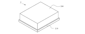
- FIG. 6 is a perspective view of the light receiving element according to the embodiment.
- FIG. 7 is a top view of the light receiving element according to the embodiment.
- FIG. 8 is a perspective view of the light emitting device according to the second embodiment.
- FIG. 9 is a perspective view of the light emitting device according to the second embodiment excluding the lid member.
- polygons such as triangles and quadrangles are referred to as polygons, including shapes in which the corners of the polygon are rounded, chamfered, chamfered, rounded, etc. It shall be called. Further, not only the corner (edge of the side) but also the shape in which the middle part of the side is processed is also referred to as a polygon. That is, the partially processed shape while leaving the polygon as the base is included in the interpretation of the "polygon" described in the present specification and the claims.
- FIG. 1 is a perspective view of the light emitting device 1.
- FIG. 2 is a perspective view showing a state in which the lid member 80 is removed from the light emitting device 1.
- FIG. 3 is a top view of a state similar to that of FIG.
- FIG. 4 is an enlarged view of a portion X of the light receiving surface 42 of the light receiving element 40 in the top view of FIG.
- FIG. 5 is a cross-sectional view taken along the VV cross-sectional line of FIG.
- FIG. 6 is a perspective view of the light receiving element 40.
- FIG. 7 is a top view of the light receiving element 40.
- the wiring region 14 provided in the stepped portion 13 of the base portion 10 is shown by hatching.
- the broken line indicating the part X is a virtual line.
- the elliptical region indicated by the dotted line on the light receiving surface 42 indicates the region to be irradiated with light.
- an example of the third central region 463 is shown by hatching having a large width, and the end region 47 based on the third central region 463 is shown by hatching having a small width.
- the third central region 463 and the alternate long and short dash line drawn to indicate the width Y are virtual lines. Further, in FIG.
- the second central region 462 is shown by hatching having a large width
- the end region 47 based on the second central region 462 is shown by hatching having a small width.
- the first central region 461, the second central region 462, the width S, the width T, and the alternate long and short dash line drawn to indicate the middle line P are virtual lines.
- the light emitting device 1 has a plurality of components including a base 10, a semiconductor laser element 20, a submount 30, a light receiving element 40, a support base 50, a protection element 60, a plurality of wirings 70, and a lid member 80 (support base). For 50, see FIG. 5 in particular).
- three semiconductor laser elements 20, a submount 30, a light receiving element 40, a support base 50, and a plurality of wirings 70 are provided in a space surrounded by a base 10 and a lid member 80. Have been placed. Further, the light emitted from the three semiconductor laser elements 20 arranged in the space is emitted to the outside of the light emitting device 1.
- the base 10 has an arrangement area, which is an area where other components are arranged, and a side wall surrounding the arrangement area. Further, the base portion 10 has a recess, and the recess is formed by an arrangement area and a side wall. The recess is recessed from the upper surface of the base 10 toward the lower surface. Here, the surface that becomes the bottom of the recess is called the bottom surface. The bottom surface can be a major part of the placement area.
- the outer shape of the base 10 is rectangular. Further, when viewed from above, the outer shape of the recessed portion is rectangular. Further, when viewed from above, the outer shape of the bottom surface of the base 10 is rectangular. The outer shape of the bottom surface is smaller than the outer shape of the recessed part. It should be noted that none of these outer shapes need be rectangular.
- the base portion 10 has a bottom surface portion 11 and a side surface portion 12.
- the bottom surface portion 11 is a portion constituting the bottom surface of the base portion 10. Further, the bottom surface portion 11 includes a bottom surface of the base portion 10 and a bottom surface.
- the side surface portion 12 is a portion constituting the side wall of the base portion 10. Therefore, the side surface portion 12 surrounds the bottom surface of the base portion 10 and extends upward from the bottom surface.
- the side surface portion 12 includes one or more outer surfaces of the base portion 10, one or more inner surfaces, and an upper surface that intersects the outer surface and the inner surface.
- the number of surfaces on the inner surface or the outer surface of the base 10 depends on the shape surrounding the bottom surface.
- the shape surrounding the bottom surface is rectangular, inner side surfaces corresponding to each of the four sides of the rectangle are formed, and the number of surfaces on the inner side surface is plural.
- the shape surrounding the bottom surface is circular, an inner surface corresponding to one circle is formed, and the number of surfaces on the inner surface is one. The same applies to the outer surface.
- the base 10 has one or more stepped portions 13.
- the step portion 13 is formed in a recessed portion of the base portion 10.
- the step portion 13 refers to a portion composed of only an upper surface and an inner side surface that intersects the upper surface and extends downward.
- the step portion 13 is included in the side surface portion 12 of the base portion 10. Further, the step portion 13 is provided below the upper surface of the base portion 10. Further, in top view, it is formed between the outer shape of the recessed portion of the base 10 and the outer shape of the bottom surface.
- the step portion 13 is formed along the inner side surface that intersects the upper surface of the base portion 10. Therefore, the inner side surface that intersects the upper surface of the base portion 10 and the upper surface of the step portion 13 intersect. Further, the step portion 13 is formed along a part of the inner side surface that intersects the upper surface of the base portion 10. In other words, the step portion 13 is not provided along the entire circumference of the inner side surface that intersects the upper surface of the base portion 10. In addition, it may be provided along the entire circumference.
- the outer shape of the inner side surface intersecting the upper surface of the base portion 10 is rectangular in top view, and the step portion 13 is provided over three sides of this rectangle. Further, one side of the rectangle is not provided with the step portion 13 except for the intersection with the other side. The number of sides along which the step portion 13 is along does not have to be three.
- the step portion 13 is preferably provided along 50% or more of the entire circumference of the inner surface surface intersecting the upper surface of the base portion 10. As a result, it is possible to secure a sufficient area for providing the wiring area in the step portion 13. Further, it is preferably 90% or less.
- the step portion 13 is not provided in the region unsuitable for providing the wiring region, and the base portion 10 can be designed to be compact. In addition, it may be provided along the entire circumference.
- One or more wiring regions 14 are provided on the upper surface of the step portion 13.
- a plurality of wiring regions 14 are provided.
- the wiring region 14 passes through the inside of the base portion 10 and is electrically connected to the wiring region provided on the lower surface of the base portion 10.
- the wiring region electrically connected to the wiring region 14 is not limited to the lower surface of the base portion 10, but can be provided on the outer surface (upper surface, outer surface, and lower surface) of the base portion 10.
- the base 10 can be formed using ceramic as the main material.
- the ceramic used for the base 10 include aluminum nitride, silicon nitride, aluminum oxide, and silicon carbide.
- the base portion 10 can be formed by integrally forming the bottom surface portion 11 and the side surface portion 12. Further, the bottom surface portion 11 and the side surface portion 12 which are separately formed by using different materials as the main materials may be joined and formed. In this case, for example, the bottom surface portion 11 may be made of metal and the side surface portion 12 may be made of ceramic as the main material.
- the metal used for the bottom surface portion 11 is preferably one having better heat dissipation (high thermal conductivity) than the ceramic used for the side surface portion 12.
- the ceramic used for the side surface portion 12 For example, copper, aluminum, iron and the like, or as a composite, copper molybdenum, copper-diamond composite material, copper tungsten and the like can be used.
- a metal film is provided at each of the wiring region 14 of the base portion 10 and the portion corresponding to the wiring region electrically connected to the wiring region 14. Further, for electrical connection, metal is also provided at a place passing through the inside, whereby electrical connection is achieved.
- the semiconductor laser device 20 has a rectangular outer shape when viewed from above. Further, the side surface that intersects with one of the two short sides of the rectangle is the emission end surface of the light emitted from the semiconductor laser element 20. Further, the upper surface and the lower surface of the semiconductor laser element 20 have a larger area than the emission end surface.
- the semiconductor laser device 20 is a multi-emitter having two or more emitters. A single emitter having one emitter may be used. In the illustrated example of the light emitting device 1, the semiconductor laser device 20 has two emitters. Further, one electrode common to the two emitters is provided on one of the upper surface and the lower surface of the semiconductor laser element 20, and two electrodes corresponding to the respective emitters are provided on the other side.
- the light (laser light) emitted from each emitter of the semiconductor laser element 20 has a spread and forms an elliptical farfield pattern (hereinafter referred to as "FFP") on a surface parallel to the emission end surface of the light.
- FFP is the shape and light intensity distribution of emitted light at a position away from the emitted end face.
- the light passing through the center of the elliptical shape of the FFP in other words, the light having the peak intensity in the light intensity distribution of the FFP is referred to as the light traveling on the optical axis.
- the light having an intensity of 1 / e 2 or more with respect to the peak intensity value is referred to as the light of the main portion.
- the shape of the FFP of the light emitted from the semiconductor laser element 20 is an elliptical shape in which the stacking direction perpendicular to the layer direction of the plurality of semiconductor layers including the active layer is longer than the layer direction.
- the layer direction is the horizontal direction of FFP
- the stacking direction is the vertical direction of FFP.
- the angle corresponding to the full width at half maximum of the light intensity distribution is defined as the light spread angle of the semiconductor laser device.
- the spread angle of light in the vertical direction of the FFP is defined as the spread angle in the vertical direction
- the spread angle of light in the horizontal direction of the FFP is referred to as the spread angle in the horizontal direction.
- the semiconductor laser element 20 for example, a semiconductor laser element that emits blue light, a semiconductor laser element that emits green light, a semiconductor laser element that emits red light, or the like can be adopted. Further, a semiconductor laser device that emits light other than these may be adopted.
- blue light refers to light whose emission peak wavelength is in the range of 420 nm to 494 nm.
- the green light refers to light whose emission peak wavelength is in the range of 495 nm to 570 nm.
- the red light refers to light whose emission peak wavelength is in the range of 605 nm to 750 nm.
- Examples of the semiconductor laser device that emits blue light or the semiconductor laser device that emits green light include a semiconductor laser device containing a nitride semiconductor.
- a semiconductor laser device containing a nitride semiconductor for example, GaN, InGaN, and AlGaN can be used.
- Examples of the semiconductor laser device that emits red light include those including InAlGaP-based, GaInP-based, GaAs-based, and AlGaAs-based semiconductors.
- the submount 30 has two joint surfaces and is composed of a rectangular parallelepiped shape. Further, the other joint surface is provided on the opposite side of one joint surface. Also, the distance between the two joint surfaces is smaller than the distance between the other two opposing surfaces.
- the shape of the submount 30 does not have to be limited to a rectangular parallelepiped.
- the submount 30 can be formed using, for example, silicon nitride, aluminum nitride, or silicon carbide. Further, a metal film for joining is provided on the joining surface.
- the light receiving element 40 has a joint surface 41 and a light receiving surface 42.
- the joint surface 41 is a surface opposite to the light receiving surface 42. It does not have to be on the opposite side.
- the light receiving element 40 has an upper surface, a lower surface, and one or more side surfaces.
- the surface having the light receiving surface 42 is the upper surface.
- the outer shape of the light receiving element 40 is a rectangular parallelepiped, but the outer shape is not limited to the rectangular parallelepiped.
- a plurality of light receiving regions 43 are provided on the light receiving surface 42.
- three light receiving regions 43 are provided.
- the number of light receiving regions 43 is not limited to three.
- the plurality of light receiving regions 43 are arranged side by side at predetermined intervals.
- the direction in which the plurality of light receiving regions 43 are lined up is referred to as the first direction.
- the arrow direction of 1D in FIG. 7 indicates a first direction based on the example of the light receiving element 40 shown.
- the light receiving surface 42 has a rectangular outer shape. Further, the length of the light receiving surface 42 in the first direction is larger than the length in the second direction.
- the second direction is a direction perpendicular to the first direction in a top view.
- the 2D arrow direction in FIG. 7 indicates a second direction based on the example of the light receiving element 40 shown.
- the length in the first direction and the length in the second direction may be the same. Further, the length in the second direction may be larger than the length in the first direction.
- the plurality of light receiving regions 43 are close to each other and lined up at regular intervals. That is, the light receiving regions 43 are separated and do not overlap. The interval does not have to be constant.
- the distance between the adjacent light receiving regions 43 is smaller than the width in the first direction in any one of the adjacent light receiving regions 43. As a result, the intervals of the light radiated to each light receiving region 43 can be brought close to each other.
- Each light receiving region 43 is formed on the light receiving surface 42 with a rectangular outer shape. It should be noted that the design is not limited to a rectangle, and may be appropriately designed according to the shape of the emitted light. In the illustrated light receiving element 40 example, each light receiving region 43 is formed with a rectangular outer shape. The two sides (short sides in the case of a rectangle) of one of the two opposing sides forming a rectangle are parallel to the first direction. The parallelism here includes an error within ⁇ 5 degrees.
- the length of the light receiving region 43 in the second direction is larger than the length in the first direction. In the illustrated example of the light emitting device 1, all the light receiving regions 43 satisfy this condition.
- the light receiving region 43 having the same length in the first direction and the second direction may be included. Further, the light receiving region 43 whose length in the first direction is larger than the length in the second direction may be included.
- the plurality of light receiving regions 43 include two light receiving regions 43 having different lengths in the second direction on the light receiving surface 42. Further, at least one of the light receiving regions 43 arranged at both ends has a smaller length in the second direction on the light receiving surface 42 than the light receiving region 43 arranged next to the light receiving region 43. Further, the lengths of the light receiving regions 43 arranged at both ends in the second direction are different.
- the light receiving element 40 can be miniaturized.
- the light receiving element 40 In the example of the light receiving element 40 shown in the figure, three light receiving regions 43 are arranged side by side in the first direction. Further, the light receiving region 43 arranged at one end of both ends has a shorter length in the second direction than the other light receiving region 43.
- the light receiving element 40 is downsized by providing a conduction region 45, which will be described later, in the space created by the difference in length.
- the lengths of all the light receiving regions 43 in the second direction may be the same. Further, all of the light receiving regions 43 arranged at both ends may have a smaller length in the second direction on the light receiving surface 42 than the light receiving regions 43 arranged next to the light receiving regions 43. Further, the lengths of the light receiving regions 43 arranged at both ends in the second direction may be the same.
- the plurality of light receiving regions 43 are arranged so that one end of either end of the light receiving region 43 in the second direction is aligned.
- the straight line connecting the end points of any one of both ends in the second direction in each light receiving region 43 is parallel to the first direction.
- the parallelism here includes a difference within ⁇ 5 degrees.
- the plurality of light receiving areas 43 include two light receiving areas 43 arranged adjacent to each other. Further, the plurality of light receiving regions 43 include two light receiving regions 43 arranged at both ends. Further, the plurality of light receiving regions 43 include two light receiving regions 43 having different lengths in the second direction. Further, the plurality of light receiving regions 43 may be all the light receiving regions 43. By aligning the positions of one end, it is possible to contribute to the miniaturization of the light receiving element 40.
- the light receiving element 40 When the light receiving element 40 has two light receiving regions 43 having different lengths in the second direction, by aligning one end, the other end is not aligned. At this time, the distance between the other end in one light receiving region 43 and the other end in the other light receiving region 43 in the second direction is the same as the difference in length between the two light receiving regions 43 in the second direction. ..
- a plurality of light receiving regions 43 in which neither end of the second direction is aligned in other words, a plurality of straight lines connecting the ends of the plurality of light receiving regions 43 in any of both ends are not parallel to the first direction. It may have a light receiving region 43 of.
- the light receiving region 43 having the shorter length in the second direction Is provided between a straight line passing through one end point of both ends in the second direction of the longer light receiving region 43 and parallel to the first direction and a straight line passing through the other end point and parallel to the first direction. Is preferable in designing the light receiving element 40 to be compact.
- a plurality of wiring regions 44 are provided on the light receiving surface 42 of the light receiving element 40.
- the number of wiring areas 44 may be 1 or more. Further, the wiring region may be provided not only on the light receiving surface 42 but also on a surface other than the light receiving surface 42. Each wiring area is electrically connected to the light receiving area 43.
- the light receiving surface 42 is provided with a plurality of wiring areas 44 that are electrically connected to the plurality of light receiving areas 43.
- the plurality of light receiving regions 43 include two light receiving regions 43 arranged adjacent to each other.
- the plurality of light receiving regions 43 include two light receiving regions 43 arranged at both ends.
- the plurality of light receiving regions 43 include two light receiving regions 43 having different lengths in the second direction.
- the plurality of light receiving regions 43 include all the light receiving regions 43 provided on the light receiving surface 42.
- a plurality of wiring regions 44 that are electrically connected to all the light receiving regions 43 arranged on the light receiving surface 42 are provided. Specifically, there are four wiring regions 44 that are electrically connected to the three light receiving regions 43. That is, the light receiving surface 42 is provided with more wiring regions 44 than the number of light receiving regions 43.
- Three of the four wiring regions 44 are electrically connected to the anode electrode of any of the three light receiving regions 43 without overlapping each other. The remaining one is electrically connected to a cathode electrode common to the three light receiving regions 43.
- the plurality of wiring regions 44 are provided in the end regions 47 on the light receiving surface 42 (shown in FIG. 7).
- the end region 47 is a region on the light receiving surface 42 excluding the central region 46.
- the first central region 461 is a straight line extending in the second direction through the midpoint of the width in the first direction in the light receiving region 43 arranged at one end of the light receiving regions 43 arranged at both ends on the light receiving surface 42. It is a region sandwiched between the light receiving region 43 arranged at the other end and a straight line extending in the second direction through the midpoint of the width in the first direction.
- the second central region 462 refers to the end point of the light receiving surface 42 located at the farthest position from the light receiving region 43 at the other end of the light receiving region 43 arranged at one end of the light receiving regions 43 arranged at both ends. It is a region sandwiched between a straight line extending in the second direction and a straight line extending in the second direction through the end point located at the farthest position from the light receiving region 43 at one end in the light receiving region 43 arranged at the other end. ..
- the first central region 461 is included in the second central region 462. Therefore, the end region 47 when the second central region 462 is the central region 46 is included in the end region 47 when the first central region 461 is the central region 46.
- the central region 46 may be a region including at least the first central region 461 or the second central region 462.
- the central region 46 here may be either the first central region 461 or the second central region 462.
- the central region 46 here may be either the first central region 461 or the second central region 462.
- the plurality of wiring regions 44 that are electrically connected to the two light receiving regions 43 having different lengths in the second direction are provided in the end region 47. Further, it is not provided in the central region 46.
- the central region 46 here may be either the first central region 461 or the second central region 462.
- the central region 46 may be either the first central region 461 or the second central region 462.
- the end region 47 is divided into two regions separated by sandwiching the central region 46.
- One region separated by the central region 46 is referred to as the first portion of the end region 47, and the other region is referred to as the second portion of the end region 47.
- One or more wiring regions 44 are provided in the first portion of the end region 47, and one or more wiring regions 44 are provided in the second portion of the end region 47.
- the wiring areas 44 By providing the wiring areas 44 on both sides, the wiring is not concentrated on one side portion, so that the distance between the wirings can be widened and the wiring becomes easy. It should be noted that a plurality of wiring areas 44 may be provided in either one of the first portion and the second portion, and the wiring area 44 may not be provided in the other portion.
- the number of wiring regions 44 provided in the first portion of the end region 47 and the number of wiring regions 44 provided in the second portion of the end region 47 are the same or one difference. By equalizing the number of the wiring areas 44 provided in this way, the distance between the wirings can be widened, and the wiring becomes easy.
- two wiring regions 44 are provided in each of the first portion and the second portion of the end region 47.
- the light receiving element 40 is provided with a plurality of conduction regions 45 on the light receiving surface 42.
- the conduction region 45 may be one, or the conduction region 45 may not be present.
- the conduction region 45 connects the light receiving region 43 and the wiring region 44. As a result, the light receiving region 43 and the wiring region 44 are electrically connected.
- the wiring region 44 and the conduction area 45 will be described.
- the wiring region 44 and the conduction region 45 may be provided with different materials, or may be provided with the same material. When provided with the same material, there may be no apparent boundary between the wiring region 44 and the conduction region 45. In such a case, the wiring area 44 may be defined as follows to specify the boundary between the wiring area 44 and the conduction area 45.
- the plurality of wiring areas 44 are areas to which the wirings for electrically connecting the light receiving areas 43 are joined.
- the bonding device specifies a position where the wiring region 44 is provided and joins the wiring. Therefore, the wiring area 44 can be defined as an area in which the wiring is actually joined based on the relationship of the connection with the wiring.
- the wiring region 44 is provided with a predetermined shape as a target of the wiring joint position.
- the wiring region 44 is defined as an region having the same shape and size as the outer shape, which is common among a plurality of regions provided on the light receiving surface 42 for electrically connecting the light receiving region 43. be able to.
- the illustrated light receiving element 40 has four regions as a plurality of regions provided on the light receiving surface 42 for electrically connecting the light receiving region 43. Further, one of them is a wiring region 44 that is electrically connected to the cathode electrode of the light receiving region 43. The remaining three are regions in which the wiring regions 44 and the conduction regions 45, which are electrically connected to the anode electrodes of the light receiving region 43, are connected to each other. Further, each light receiving region 44 is a region having a rectangular shape and size having the same outer shape.
- the shape of the area provided as the target of the wiring joint position does not have to be the same. Even in this case, it is necessary to secure the minimum area that must be secured for wiring connection. Therefore, when there is no commonality in the outer shapes, when each of the plurality of regions provided on the light receiving surface 42 for electrically connecting the light receiving region 43 is overlapped, the maximum range that overlaps in all the regions is set. It can be defined as the wiring area 44. In the example of the light receiving element 40 shown in the figure, the maximum range in which all four regions can be overlapped is the wiring region 44.
- a region excluding the wiring region 44 from the region provided on the light receiving surface 42 for electrically connecting the light receiving region 43 can be defined as the conduction region 45. it can.
- the boundary between the wiring area 44 and the conduction area 45 is not limited to the method described here. It may be determined by a method that can be reasonably interpreted, such as when it can be clearly distinguished from the viewpoint of appearance and material, or when it can be clearly distinguished from the manufacturing process of the light receiving element 40.
- each conducting region 45 in the second direction is shorter than the length of the light receiving region 43 in the second direction. Further, it is shorter than the length of the wiring region 44 in the second direction. Further, the plurality of conduction regions 45 include a conduction region 45 whose length in the first direction is longer than the length in the first direction of one light receiving region 43. Further, the plurality of conduction regions 45 include a conduction region 45 whose length in the first direction is shorter than the length in the first direction of one light receiving region 43.
- the light receiving surface 42 is provided with a plurality of conduction regions 45 connecting the plurality of light receiving regions 43 and the plurality of wiring regions 44. Further, the plurality of light receiving regions 43 include two light receiving regions 43 arranged adjacent to each other. Further, the plurality of light receiving regions 43 include two light receiving regions 43 arranged at both ends. Further, the plurality of light receiving regions 43 include two light receiving regions 43 having different lengths in the second direction.
- the plurality of light receiving regions 43 include all the light receiving regions 43 provided on the light receiving surface 42. Further, the plurality of wiring areas 44 do not include one or more wiring areas 44 among all the wiring areas 44 provided on the light receiving surface 42. It should be noted that the entire wiring region 44 provided on the light receiving surface 42 may be included.
- a plurality of conduction regions 45 connected to each of all the light receiving regions 43 arranged on the light receiving surface 42 are provided. Specifically, there are three conduction regions 45 connected to the three light receiving regions 43. That is, the number of light receiving regions 43 arranged on the light receiving surface 42 and the number of conductive regions 45 are equal.
- the conduction region 45 connects the light receiving region 43 and the wiring region 44 that is electrically connected to the anode electrode of the light receiving region 43.
- the wiring region 44 that is electrically connected to the cathode electrode of the light receiving region 43 is not connected to the conduction region 45.
- the wiring region 44 is electrically connected to the cathode electrode of the light receiving region 43 inside the light receiving element 40.
- the number of conduction regions 45 provided on the light receiving surface 42 can be reduced, which contributes to the compact design of the light receiving element 40. Can be done. It may have a conduction region 45 connecting the cathode electrode of the light receiving region 43 and the wiring region 44.
- the plurality of conduction regions 45 include a conduction region 45 provided from the central region 46 to the end region 47. Further, the plurality of conduction regions 45 include a conduction region 45 provided in the end region 47 and not provided in the central region 46.
- the central region 46 here may be either the first central region 461 or the second central region 462.
- the plurality of conduction regions 45 are connected to one of the two light receiving regions 43 arranged adjacent to each other, and are provided from the central region 46 to the end region 47, and the other of the conduction regions 45. It includes a conduction region 45 that is connected to the light receiving region 43 and is not provided in the central region 46 but is provided in the end region 47.
- the other light receiving region 43 is a light receiving region 43 arranged at the end of a plurality of light receiving regions 43 arranged side by side in the first direction.
- the conductive region 45 provided from the central region 46 to the end region 47 and the end region 47 not provided in the central region 46.
- the conductive region 45 provided extends from a position connected to the light receiving region 43 in the first direction and is connected to the wiring region 44.
- Each of the wiring regions 44 is provided in the first portion and the second portion of the end region 47, whichever is closer to the light receiving region 43 arranged at the end.
- the conduction region 45 provided from the central region 46 to the end region 47 is connected to the side of one of the two opposing sides of the two light receiving regions 43 arranged adjacent to each other. Further, it extends from the position connected to this side in the first direction in parallel with the first direction and is connected to the wiring area 44.
- the light receiving element 40 is connected to a straight line parallel to the second direction through one end connected to the light receiving region 43 and a wiring region 44 among both ends of the conductive region 45 provided from the central region 46 to the end region 47. It has a light receiving region 43 sandwiched between a straight line passing through the end and parallel to the second direction.
- the light receiving region 43 having the shorter length in the second direction is provided in the range of the width S shown in the figure.
- the conduction region 45 which is electrically connected to one of the two light receiving regions 43 arranged adjacent to each other and is provided from the central region 46 to the end region 47, is different from the other light receiving region 43. Do not connect electrically.
- a method of avoiding electrical connection there is a method of providing an insulating region in a part of the other light receiving region 43 and providing a conductive region 45 on the insulating region. Since the insulating region is provided on the light receiving region 43, the position where the insulating region is provided can be adjusted.
- the conduction region 45 is connected to the one light receiving region 43 at a portion protruding from the other light receiving region 43 in the second direction, and extends in a direction parallel to the first direction. It connects to the wiring area 44.
- the conduction region 45 which is not provided in the central region 46 but is provided in the end region 47, is an adjacent light receiving region 43 in the light receiving region 43 arranged at the end of the two light receiving regions 43 arranged adjacent to each other. It connects to the side opposite to the side facing.
- the conduction region 45 provided from the central region 46 to the end region 47 is connected to the light receiving region 43 near the upper end or the lower end of the light receiving region 43. This is because the closer to the end, the more the other light receiving region 43 can be suppressed from being reduced, and a wider light receiving region can be secured.
- the wiring region 44 is a straight line extending in the first direction through one end of both ends at the most end in the second direction among the plurality of light receiving regions 43, and the first direction passing through the other end. It is preferable that it is provided in a region sandwiched between a straight line extending in. It is possible to prevent the light receiving element 40 from becoming large in the second direction. In the example of FIG. 7, all the wiring regions 44 are within the range of the width T shown in the figure. The same can be said even if the wiring region 44 is replaced with the conduction region 45.
- the wiring region 44 is provided not near the center of the light receiving surface 42 but near one end of the light receiving surface 42 in the second direction.
- both the wiring region 44 closest to one end of both ends at the end in the second direction and the wiring region 44 closest to the other end are the other. It is preferably located closer to one end than the end. Further, it is preferable that the same can be said even if the plurality of light receiving regions 43 are replaced with the light receiving surfaces 42.
- the wiring region 44 located closest to one end of both ends which is the farthest end in the second direction among the plurality of light receiving regions 43, is provided at a position closer to this one end than the center of both ends. Moreover, it is preferable that the wiring region 44 closest to the other end is provided at a position closer to the center of both ends than the other end. Further, it is preferable that the same can be said even if the plurality of light receiving regions 43 are replaced with the light receiving surfaces 42.
- the virtual line P shown in the figure shows the center lines of both ends at the most end in the second direction among the plurality of light receiving regions 43.
- the virtual line P indicates the center line of the light receiving surface 42.
- one of the two wiring regions 44 in the first portion of the end region 47 becomes the wiring region 44 closest to one end at both ends, and the other is the position closest to the other end at both ends. It becomes the wiring area 44 in, and satisfies these. The same can be said if the first part is replaced with the second part.
- the light receiving element 40 for example, a photodiode (hereinafter, PD, which is abbreviated as abbreviation) can be adopted. Further, the light receiving element 40 reflects 80% or more of the light irradiated to the light receiving region 43.
- PD photodiode
- the support base 50 has a lower surface and an inclined surface 51 inclined with respect to the lower surface.
- the inclined surface 51 is neither vertical nor parallel when viewed from the lower surface.
- the inclined surface 51 is composed of a plane having an inclination angle of 40 degrees or more and 50 degrees or less with respect to the lower surface.
- the inclined surface 51 is formed of a plane having an inclination angle of 45 degrees with respect to the lower surface.
- the inclined surface 51 may be formed in a range where the inclination angle is 10 degrees or more and 80 degrees or less.
- the inclined surface 51 is one or a plurality of inclined surfaces that are inclined with respect to the lower surface of the support base 50, and is the inclined surface having the largest area when there are a plurality of inclined surfaces. Further, the inclined surface 51 occupies an area of 60% or more of the support base 50 when viewed from above. Further, when viewed from above, the width from the upper end to the lower end of the inclined surface 51 is 60% or more of the width of the support base 50 in the same direction. That is, the support base 50 is mainly occupied by the inclined surface 51.
- the support base 50 can be formed by using, for example, ceramic, glass, metal, or the like.
- ceramics such as aluminum nitride, glass such as quartz or borosilicate glass, and metals such as aluminum can be used. Alternatively, it can also be formed using Si or the like.
- the protective element 60 is for preventing an excessive current from flowing to a specific element (for example, the semiconductor laser element 20) and destroying the element.
- Examples of the protection element 60 include a Zener diode. Further, as the Zener diode, a diode made of Si can be adopted.
- the wiring 70 has a linear shape with both ends as joints. That is, it has joints at both ends of the linear portion to join with other components.
- the wiring 70 is, for example, a metal wire.
- the metal for example, gold, aluminum, silver, copper and the like can be used.
- the lid member 80 has a lower surface and an upper surface, and is formed of a rectangular parallelepiped flat plate shape. It does not have to be a rectangular parallelepiped. Further, the lid member 80 has a translucent property that transmits light. Here, the translucency means that the transmittance with respect to light is 80% or more. It is not necessary to have a transmittance of 80% or more for light of all wavelengths. Further, the lid member 80 may have a non-translucent region (a region having no translucency) in a part thereof.
- the lid member 80 can be formed using sapphire.
- Sapphire is a material that has translucency, has a relatively high refractive index, and has a relatively high strength.
- glass or the like can also be used.
- the light emitting device 1 includes a base 10, a semiconductor laser element 20 arranged on the base 10, a light receiving element 40 arranged on the base 10, and a plurality of semiconductor laser elements 20 among a plurality of wirings 70 for electrically connecting. It has a first wiring 71 and a plurality of second wirings 72 for electrically connecting the light receiving element 40 of the plurality of wirings 70.
- the semiconductor laser element 20 another light emitting element such as an LED may be used.
- the semiconductor laser element 20 is arranged on the base 10 via the submount 30. In addition, it may be arranged directly on the bottom surface of the base portion 10 without passing through the sub mount 30. When the submount 30 is not used, the outer shape of the semiconductor laser element 20 may be changed in order to adjust the light emission position (height) on the emission end face.
- the light receiving element 40 is arranged on the base 10 via the support base 50. It should be noted that it may be arranged directly on the bottom surface of the base 10 without going through the support base 50. If the support base 50 is not used, the outer shape of the light receiving element 40 may be changed in order to adjust the position (height) and orientation (tilt) of the light receiving surface 42.
- the light emitting device 1 is arranged at the base 10 and has a protective element 60 that protects the semiconductor laser element 20. Further, the light emitting device 1 has a lid member 80 that is joined to the base portion 10 and seals the space in which the semiconductor laser element 20 is arranged.
- the semiconductor laser element 20 is arranged on the bottom surface (arrangement region) of the base 10. Further, a plurality of semiconductor laser elements 20 may be arranged. Further, the plurality of semiconductor laser elements 20 are arranged side by side so that the emission end faces face the same direction. Further, between the adjacent semiconductor laser elements 20, the side surfaces that intersect with the respective emission end faces face each other.
- the direction in which the plurality of semiconductor laser elements 20 are lined up in the top view is referred to as the first direction.
- the direction perpendicular to the first direction in the top view is referred to as the second direction.
- the first direction and the second direction based on the example of the illustrated light emitting device 1 are shown by 1D and 2D in FIG. 3, respectively.
- the direction in which the plurality of emitters are lined up may be referred to as the first direction.
- the first direction is parallel to the emission end surface of the semiconductor laser element 20 in a top view.
- the side surfaces that intersect with each emission end surface and face each other between the adjacent semiconductor laser elements 20 are parallel in top view.
- the three semiconductor laser elements 20 are composed of a semiconductor laser element that emits blue light, a semiconductor laser element that emits green light, and a semiconductor laser element that emits red light.
- the configuration is not limited to this, and a configuration having a plurality of semiconductor laser elements that emit light of the same color may be used, or a configuration having semiconductor laser elements that emit light of other colors may be used.
- the submount 30 is bonded to the semiconductor laser element 20 at one of the bonding surfaces. Further, the other joint surface on the opposite side is joined to the bottom surface of the base portion 10.
- the light emitting device 1 may have a plurality of submounts 30. The number of semiconductor laser elements 20 arranged in one submount 30 may be one.
- the light receiving element 40 is arranged on the bottom surface of the base 10. Further, the light receiving surface 42 is arranged in the direction in which the light emitted from the semiconductor laser element 20 is irradiated. Further, the plurality of light receiving regions 43 of the light receiving surface 42 are irradiated with the light of the main portion emitted from the semiconductor laser element 20. Further, one light receiving region 43 is irradiated with light of a main portion of at least one laser beam. That is, the light of the main part of the two laser beams may be irradiated.
- the plurality of light receiving regions 43 provided on the light receiving surface 42 of the light receiving element 40 are irradiated with the light emitted from the plurality of semiconductor laser elements 20. Further, one light receiving region 43 corresponds to one semiconductor laser element 20, and one light receiving region 43 is irradiated with light of a main portion emitted from one semiconductor laser element 20.
- the three light receiving regions 43 are irradiated with the light of at least the main part of the light emitted from the three semiconductor laser elements 20. Further, one light receiving region 43 is irradiated with two laser beams emitted from each of the two emitters of one semiconductor laser element 20.
- the light receiving element 40 receives (absorbs) a part of the light radiated to the light receiving region 43 and reflects a part of the light.
- the light receiving region 43 receives 2% or more of the light of the irradiated main portion. Further, the light receiving region 43 reflects 80% or more of the light of the irradiated main portion. The sum of the received light and the reflected light is 100% or less.
- first direction in the light emitting device 1 and the first direction in the light receiving element 40 are the same direction and are parallel. Further, in top view, the emission end surface of the semiconductor laser element 20 and the lower end side or the upper end side of the light receiving surface 42 of the light receiving element 40 are parallel to each other. Parallelism here includes a difference of up to 5 degrees. It does not have to be parallel.
- the light receiving region 43 reflects the light emitted laterally from the semiconductor laser element 20 upward. Therefore, the light receiving surface 42 is tilted with respect to the emission end surface and the optical axis. It also tilts with respect to the bottom surface of the base 10.
- the light receiving surface 42 is tilted at an angle of 40 degrees or more and 50 degrees or less with respect to the traveling direction of light passing through the optical axis. In the illustrated example of the light emitting device 1, it is tilted at an angle of 45 degrees. It may be tilted at an angle in the range of 10 degrees or more and 80 degrees or less.
- the wiring region 44 of the light receiving element 40 is arranged at a position where it does not enter the optical path of the light of the main portion emitted from the semiconductor laser element 20. Further, the second wiring 72 joined to the wiring region 44 is arranged at a position where it does not enter the light path of the main portion.
- the end region 47 here is an region excluding the central region 46, and a third central region 463 is defined as the central region 46 here.
- the third central region 463 is a top view of the light passing through the optical axis of the light radiating to the light receiving region 43 arranged at one end of the light receiving regions 43 arranged at both ends on the light receiving surface 42. It is sandwiched between a straight line extending in the second direction through the irradiation point and a straight line extending in the second direction through the irradiation point of the light passing through the optical axis among the light emitted to the light receiving region 43 arranged at the other end.
- the area It may be at least a region including this region.
- the provision of the third central region 463 may be satisfied based on at least one of the laser beams. Further, it is preferable that the provision of the third central region 463 is satisfied based on the laser beam radiated to both ends in the first direction. In the example of FIG. 4, the third central region 463 based on the laser beam radiated to both ends is shown by hatching.
- the plurality of light receiving regions 43 in the light receiving element 40 include two light receiving regions 43 having different lengths in the second direction, the spread angles of the plurality of laser beams emitted from the semiconductor laser element 20 in the vertical direction are increased. Therefore, the light receiving region 43 to be irradiated with the laser beam may be determined. This is because the laser beam having a large spread angle in the vertical direction forms a longer irradiation region in the second direction in the light receiving region 43.
- the light of the main portion of the laser beam having the largest vertical light spread angle among the plurality of laser beams irradiates the longer light receiving region 43 of the two light receiving regions 43 having different lengths in the second direction. It is good to be done. In other words, the light of the main portion of the laser beam having the largest vertical light spread angle among the plurality of laser beams is in the shorter light receiving region of the two light receiving regions 43 having different lengths in the second direction. Is preferably not irradiated.
- the light receiving region 43 arranged at one end of the light receiving regions 43 arranged at both ends of the plurality of light receiving regions 43 arranged in the first direction is in the second direction.
- the length is smaller than the length of the light receiving region 43 arranged next to the light receiving region 43 in the second direction.
- the light of the main portion emitted from the semiconductor laser element 20 having the largest vertical light spread angle among the plurality of semiconductor laser elements 20 is the light receiving region 43 arranged at one end of both ends and is adjacent to the light receiving region 43.
- the light receiving region 43 having a length smaller than that of the light receiving region 43 arranged in the second direction is not irradiated, and the other light receiving region 43 having a length in the second direction larger than this light receiving region 43 is irradiated.
- the semiconductor laser element 20 and the light receiving element 40 are arranged.
- the light of the main portion emitted from the semiconductor laser element 20 that emits red light having the largest vertical light spread angle is in the second direction of both ends.
- the light receiving region 43 at the end having the larger length is irradiated.
- the light receiving region 43 sandwiched between both ends is also the light receiving region 43 having a larger length in the second direction, but it is preferable to arrange the semiconductor laser element 20 which is more susceptible to heat than the others at the end. ..
- the semiconductor laser device 20 that emits red light is more affected by heat than the semiconductor laser device 20 that emits blue light and the semiconductor laser device 20 that emits green light. It has easy light emission characteristics.
- the conduction region 45 provided from the first central region 461 or the second central region 462 to the end region 47 is provided from the third central region 463 to the end region 47.
- the conduction region 45 provided from the central region 46 to the end region 47 is provided near the upper end of the light receiving region 43 arranged at the end of the light emitting device 1.
- the conduction region 45 is also arranged at a position where it does not enter the optical path of the light of the main portion emitted from the semiconductor laser element 20.
- the conduction region 45 provided from the central region 46 to the end region 47 extends in the first direction on the light receiving surface 42 through the upper end of the light receiving region 43 arranged next to the light receiving region 43 arranged at the end. It is provided below the straight line and above the upper end of the light of the main portion irradiated to the light receiving region 43 arranged at the end, and connects the light receiving region 43 arranged adjacent to the light receiving region 43 and the wiring region 44.
- the conduction region 45 provided from the central region 46 to the end region 47 may be provided near the lower end of the light receiving region 43 arranged at the end of the light emitting device 1.
- the conduction region 45 irradiates the light receiving region 43 arranged at the end and above the straight line extending in the first direction through the lower end of the light receiving region 43 arranged next to the light receiving region 43 arranged at the end.
- the light receiving area 43 and the wiring area 44 which are provided below the lower end of the light of the main portion and are arranged next to each other, are connected to each other.
- the support base 50 is joined to the light receiving element 40 on the inclined surface 51. That is, the light receiving element 40 is arranged on the inclined surface 51. Further, the support base 50 is arranged so that the inclined surface 51 faces the semiconductor laser element 20. By arranging the light receiving element 40 via the support base 50, it is not necessary to form the light receiving element 40 in a complicated shape. Therefore, it is preferable that the support base 50 is made of a material that is easier to shape than the light receiving element 40.
- the support base 50 is joined to the bottom surface of the base 10 on the lower surface.
- the inclined surface 51 is inclined with respect to the bottom surface.
- the inclination angle of the inclined surface 51 with respect to the bottom surface of the base portion 10 is the same as the inclination angle of the inclined surface 51 with respect to the lower surface of the support base 50.
- the light receiving element 40 Since the light receiving element 40 is irradiated with the light emitted from the semiconductor laser element 20 and spread, it is necessary to provide the light receiving surface 42 from a position lower to a position higher than the light emitting point of the semiconductor laser element 20. Therefore, the height of the lower end of the light receiving surface 42 of the light receiving element 40 arranged in the light emitting device 1 is lower than the light emitting point of the semiconductor laser element 20, and the height of the upper end of the light receiving surface 42 is the light of the semiconductor laser element 20. It will be higher than the exit point of.
- the step portion 13 is provided at a position separated from the semiconductor laser element 20 or the light receiving element 40 in the first direction. Further, the semiconductor laser element 20 or the light receiving element 40 is provided at positions separated from each other in both directions in the first direction.
- the step portion 13 is provided with the semiconductor laser element 20 and the light receiving element 40 sandwiched in parallel in a top view.
- the step portion 13 is provided at a position separated from the semiconductor laser element 20 or the light receiving element 40 in the second direction. Further, it is provided at a position separated in the direction from the light receiving element 40 to the semiconductor laser element 20 in both directions of the second direction. It may not be provided.
- the step portion 13 provided at a position separated from the semiconductor laser element 20 or the light receiving element 40 in both directions in the first direction and in one direction in the second direction is connected. It does not have to be connected. Further, the step portion 13 is not provided at a position separated from the semiconductor laser element 20 or the light receiving element 40 in the other direction of the second direction. In addition, it may be provided.
- the wiring region 14 is provided at a position separated from the semiconductor laser element 20 or the light receiving element 40 in the first direction. Further, the wiring region 14 is provided at a position separated from the semiconductor laser element 20 or the light receiving element 40 in both directions in the first direction.
- the wiring region 14 is provided at a position separated from the semiconductor laser element 20 or the light receiving element 40 in the second direction. Further, it is provided at a position separated in the direction from the light receiving element 40 to the semiconductor laser element 20 in both directions of the second direction. It may not be provided.
- One end of both ends of the first wiring 71 is joined to the wiring region 14. The other end of both ends is joined to the upper surface of the semiconductor laser element 20 or the upper surface of the submount 30.
- a bonding region for bonding with the first wiring 71 is provided on the upper surface of the semiconductor laser element 20 or the upper surface of the submount 30.
- the upper surface of the stepped portion 13 of the base 10 is equal to or higher than the upper surface of the submount 30 in the height direction (vertical direction). It is preferably below the upper surface of. By doing so, it becomes easy to connect the first wiring 71. It is not necessary that all of the plurality of first wirings 71 are joined to the wiring region 14 of the step portion 13. One or more ends of the first wiring 71 are joined to the wiring region 14.
- the first wiring 71 includes a side surface on the semiconductor laser element 20 side (a side surface opposite to the emission end surface of the semiconductor laser element 20) with a straight line parallel to the light emitting end surface of the semiconductor laser element 20 as a boundary in top view. On the side), it is joined to the wiring region 14 of the base 10. This makes it easier to prevent the first wiring 71 from entering the optical path of light.
- One end of both ends of the second wiring 72 is joined to the wiring region 14. Further, the other end of both ends is joined to the wiring region 44 of the light receiving element 40.
- the wiring region 44 in the end region 47 the distance between the wiring region 14 of the base 10 and the wiring region 44 of the light receiving element 40 can be shortened, and the length of the second wiring 72 can be shortened. Further, the height of the second wiring 72 can be suppressed, and a light emitting device having a reduced height can be realized.
- a plurality of second wirings 72 are joined to the wiring area 14 of the base 10 and the wiring area 44 of the light receiving element 40. Further, all the wiring used for the electrical connection of the light receiving element 40 is joined to the wiring region 14. It should be noted that all the wiring used for the electrical connection of the light receiving element 40 does not have to be joined to the wiring region 14. One or more ends of the second wiring 72 are joined to the wiring region 14.
- the second wiring 72 is joined to the wiring region 14 of the base 10 on the light receiving element 40 side with a straight line parallel to the light emitting end surface of the semiconductor laser element 20 as a boundary in the top view. This makes it easier to prevent the second wiring 72 from entering the optical path of light.
- At least one or more of the second wirings 72 among the plurality of second wirings 72 are straight lines extending in the first direction through one end of both ends which are the most extreme ends in the second direction of the light receiving element 40 in the top view. , Is joined to the wiring region 14 of the base 10 within the region sandwiched by the straight line extending in the first direction through the other end. It is preferable that a plurality of second wiring 72s, and more preferably all the second wirings 72, are joined to the wiring region 14 within this region. As a result, the length of the second wiring 72 can be suppressed.
- At least one or more of the second wirings 72 among the plurality of second wirings 72 are straight lines extending in the first direction through one end of both ends which are the most extreme ends in the second direction of the light receiving surface 42 in the top view. , Is joined to the wiring region 14 of the base 10 within the region sandwiched by the straight line extending in the first direction through the other end. It is preferable that a plurality of second wiring 72s, and more preferably all the second wirings 72, are joined to the wiring region 14 within this region. Similarly, the length of the second wiring 72 can be suppressed.
- the region of the width Y is a straight line extending in the first direction through one end of both ends at the farthest end in the second direction of the light receiving surface 42 and a straight line extending in the first direction through the other end.
- all the second wirings 72 are joined to the wiring region 14 of the base portion 10.
- the position of joining with the wiring region 44 of the light receiving element 40 is higher than that of the submount 30.
- the height of the second wiring 72 in the wiring region 44 from the bottom surface of the base 10 is rather than the height from the bottom surface of the base 10 to the top surface of the submount 30. The height to the joint is larger.
- the light receiving element 40 has the wiring region 44 closer to one end of the wiring region 44, not closer to the center. Therefore, the second wiring 72 can be joined at a position closer to the upper side of the light receiving element 40, and can be joined at a position higher than the upper surface of the submount 30.
- the bonding device it is necessary to arrange the bonding device so that it does not come into contact with the semiconductor laser element 20, but by moving the wiring region 44 above the light receiving element 40, the light receiving element 40 is brought into the semiconductor laser element 20. Can be placed close together.
- the light emitting device 1 there is no wiring that passes directly above the upper end of the light receiving element 40. That is, even if further wiring is arranged in addition to the wiring 70, all the wiring arranged in the recessed portion of the base portion 10 does not pass directly above the upper end of the light receiving element 40. Therefore, the second wiring 72 is joined to the wiring region 14 and the wiring region 44 without passing directly above the upper end of the light receiving element 40. As a result, the height of the wiring can be suppressed and the height of the light emitting device 1 can be reduced.
- the second wiring 72 is joined to the wiring region 14 and the wiring region 44 without passing through the region directly above the light receiving surface 42. This makes it easier to prevent the second wiring 72 from entering the optical path of light.
- the number of the first wiring 71 related to the electrical connection of the semiconductor laser element 20 is larger than the number of the second wiring 72 related to the electrical connection of the light receiving element 40. ..
- the wiring region 14 By providing the wiring region 14 at a position separated from the light receiving element 40 toward the semiconductor laser element 20 in both directions of the second direction, a region for joining the first wiring 71 is secured, and the wiring can be easily joined. ing.
- the protective element 60 is arranged on the upper surface of the step portion 13. By arranging it on the step portion 13, the arrangement area can be reduced, which can contribute to the miniaturization of the light emitting device 1. Further, a plurality of protective elements 60 are arranged on the upper surface of the step portion 13.
- one or more protective elements 60 are arranged on both the semiconductor laser element 20 side and the light receiving element 40 side with a straight line parallel to the light emitting end surface of the semiconductor laser element 20 as a boundary. Further, the number of protective elements 60 arranged on the semiconductor laser element 20 side is larger than the number of protective elements 60 arranged on the light receiving element 40 side. Since the area where the wiring area 14 can be secured is larger on the semiconductor laser element 20 side, it is easy to join the wirings of the first wiring 71 and the second wiring 72.
- the second wiring 72 and the protection element 60 are arranged in the wiring region 14 in this order in the direction toward the light receiving element 40 with a straight line parallel to the light emitting end surface of the semiconductor laser element 20 as a boundary. To. By arranging them in this order, it becomes easy to join the second wiring 72 with a reduced length. The order may be reversed.
- the lid member 80 is arranged on the upper surface of the base 10. Further, the lid member 80 is located above the stepped portion 13. Further, by joining the lid member 80, a closed space surrounded by the base portion 10 and the lid member 80 is created. This space is a space in which the semiconductor laser element 20 is arranged. In the illustrated example of the light emitting device 1, the lid member 80 and the base portion 10 are joined, and a plurality of semiconductor laser elements 20 arranged on the base portion 10 are sealed.
- the lid member 80 by joining the lid member 80 to the base 10 under a predetermined atmosphere, an airtightly sealed closed space is created.
- an airtightly sealed closed space is created.
- the lid member 80 has translucency with respect to the light emitted from the semiconductor laser element 20.
- the light emitting device 1 80% or more of the light of the main part emitted from all the semiconductor laser elements 20 which are arranged side by side in the first direction in the light emitting device 1 and irradiate the light receiving element 40 with the light of the main part is upward. It is emitted to the outside toward the outside
- the light emitting device 1 can control the output of light emitted from the semiconductor laser element 20 based on the result of receiving light by the light receiving element 40. Thereby, the output of the light emitted from the light emitting device 1 can be controlled.
- FIG. 8 is a perspective view of the light emitting device 2.
- FIG. 9 is a perspective view showing a state in which the lid member 280 is removed from the light emitting device 2.
- the light emitting device 2 has a plurality of components including a base 210, a semiconductor laser element 20, a submount 30, a light receiving element 40, a support base 50, a plurality of wirings 70, and a lid member 280. Further, the light emitting device 2 of the second embodiment is different from the light emitting device 1 of the first embodiment in that the shapes of the base 210 and the lid member 280 are different.
- the base 210 does not have a side surface 12. Further, the base 210 is formed of a flat plate having an upper surface, a lower surface, and a side surface. Further, the surface on which the semiconductor laser element 20 is arranged and the surface on which the wiring region 14 is provided are on the same plane. It does not have to be on the same plane. For example, it may be a base portion having a step portion 13 but not having an upper surface above the step portion 13.
- the base portion 210 does not have the side surface portion 12, when the wiring 70 is joined to the wiring region 14, a certain distance is secured from the side surface portion 12 so that the joining device for joining the wiring 70 does not come into contact with the side surface portion 12. There is no need to consider such things as doing so.
- the lid member 280 is formed in a cap shape having a side wall. Further, the side wall surrounds the arrangement area and the wiring area 14. Further, the side wall is formed to a position higher than any of the semiconductor laser element 20, the light receiving element 40, and the wiring 70 arranged on the base 210.
- the lid member 280 is joined to the upper surface of the base 210, and the space in which the semiconductor laser element 20 is arranged becomes an airtightly sealed closed space.
- the light emitting device according to the present invention is not strictly limited to the light emitting device according to the embodiment. That is, the present invention cannot be realized unless it is limited to the outer shape and structure of the light emitting device disclosed by the embodiment.
- it may be a light emitting device having no protective element.
- it can be applied without being required to have all the components necessary and sufficient.
- the part of the components may be replaced, omitted, deformed in shape, or changed in material. It recognizes the degree of freedom of design by those skilled in the art and specifies that the invention described in the claims is applied.
- the light emitting device described in each embodiment can be used for a head-mounted display, a projector, an in-vehicle headlight, a lighting, a display, and the like.
Abstract
Provided is a light-receiving element (40) having a length suppressed in a direction perpendicular to a direction where light-receiving regions (43) are arrayed. This light-receiving element (40) has a light-receiving surface (42) provided with a plurality of light-receiving regions (43) arrayed in a first direction and a plurality of wiring regions (44) electrically connected to the light-receiving regions (43). Among wiring regions (44), the wiring regions (44) that are electrically connected to the light-receiving regions (43) are provided to end regions, other than a central region, in the light-receiving surface (42).
Description
本開示は、受光素子、及び、発光装置に関する。
The present disclosure relates to a light receiving element and a light emitting device.
従来、発光素子から出射された光の一部を受光素子に受光させ、その受光結果に基づいて光学制御を行う光学ユニットが知られている。また、特許文献1には、3つの受光部が並べて配置され、各受光部に係るメタル電極が設けられた受光素子が開示されている。
Conventionally, there is known an optical unit in which a part of the light emitted from a light emitting element is received by a light receiving element and optical control is performed based on the light receiving result. Further, Patent Document 1 discloses a light receiving element in which three light receiving parts are arranged side by side and a metal electrode related to each light receiving part is provided.
受光素子に複数の受光領域を設ける場合、複数の受光領域と、複数の受光領域に係る配線領域との配置関係には改善の余地がある。
When a plurality of light receiving regions are provided in the light receiving element, there is room for improvement in the arrangement relationship between the plurality of light receiving regions and the wiring region related to the plurality of light receiving regions.
本開示の受光素子は、第1方向に並べて配置される複数の受光領域と、前記複数の受光領域と電気的に接続する複数の配線領域と、が設けられる受光面を有する受光素子であって、前記複数の配線領域のうち、隣り合って配置される2つの受光領域と電気的に接続する複数の配線領域は、前記受光面において、中央領域を除いた領域である端領域に設けられ、前記中央領域は、前記受光面において、両端に配置された前記受光領域のうちの一方の端に配置された前記受光領域における前記第1方向の幅の中点を通り前記第1方向に垂直な第2方向に伸びる直線と、他方の端に配置された前記受光領域における前記第1方向の幅の中点を通り前記第2方向に伸びる直線と、に挟まれる領域を含む。
The light receiving element of the present disclosure is a light receiving element having a light receiving surface provided with a plurality of light receiving regions arranged side by side in the first direction and a plurality of wiring regions electrically connected to the plurality of light receiving regions. Of the plurality of wiring regions, a plurality of wiring regions that are electrically connected to two light receiving regions arranged adjacent to each other are provided in an end region that is a region excluding the central region on the light receiving surface. The central region is perpendicular to the first direction through the midpoint of the width of the first direction in the light receiving region arranged at one end of the light receiving regions arranged at both ends on the light receiving surface. It includes a region sandwiched between a straight line extending in the second direction and a straight line extending in the second direction through the midpoint of the width of the first direction in the light receiving region arranged at the other end.
また、本開示の受光素子は、第1方向に並べて配置される複数の受光領域と、前記複数の受光領域と電気的に接続する複数の配線領域と、が設けられる受光面を有する受光素子であって、前記複数の配線領域のうち、両端に配置される2つの受光領域と電気的に接続する複数の配線領域は、前記受光面において、中央領域を除いた領域である端領域に設けられ、かつ、前記中央領域には設けられず、前記中央領域は、前記受光面において、両端に配置された前記受光領域のうちの一方の端に配置された前記受光領域において他方の端の前記受光領域から最も遠い位置にある端点を通り前記第1方向に垂直な第2方向に伸びる直線と、他方の端に配置された前記受光領域において一方の端の前記受光領域から最も遠い位置にある端点を通り前記第2方向に伸びる直線と、に挟まれる領域を含む。
Further, the light receiving element of the present disclosure is a light receiving element having a light receiving surface provided with a plurality of light receiving regions arranged side by side in the first direction and a plurality of wiring regions electrically connected to the plurality of light receiving regions. Therefore, among the plurality of wiring regions, a plurality of wiring regions that are electrically connected to the two light receiving regions arranged at both ends are provided at the end regions that are regions excluding the central region on the light receiving surface. In addition, the central region is not provided in the central region, and the central region is the light receiving region of the light receiving region arranged at one end of the light receiving regions arranged at both ends on the light receiving surface. A straight line extending in the second direction perpendicular to the first direction through the end point located farthest from the region, and an end point located at the farthest position from the light receiving region at one end in the light receiving region arranged at the other end. Includes a region sandwiched between a straight line extending in the second direction through the above.
本開示の発光装置は、それぞれが、上面と、下面と、光が出射される出射端面を含む側面とを有し、第1方向に並べて配置される複数の発光素子と、前記第1方向に並べて配置され前記複数の発光素子から出射された光が照射される複数の受光領域と、複数の第1配線領域と、が設けられる受光面を有する受光素子と、複数の第2配線領域を有し、前記複数の発光素子と前記受光素子とが配置される基部と、それぞれが、両端のうちの一端が前記複数の第1配線領域のいずれかに接合され、他端が前記複数の第2配線領域のいずれかに接合される、複数の配線と、を有し、前記複数の第1配線領域は、前記受光面において、中央領域を除いた領域である端領域に設けられ、前記中央領域は、上面視で、前記受光面において、両端に配置された前記受光領域のうちの一方の端に配置された前記受光領域に照射される光のうち光軸を通る光の照射点を通り前記第1方向に垂直な方向である第2方向に伸びる直線と、他方の端に配置された前記受光領域に照射される光のうち光軸を通る光の照射点を通り前記第2方向に伸びる直線と、に挟まれる領域を含む。
Each of the light emitting devices of the present disclosure has an upper surface, a lower surface, and a side surface including an emission end surface from which light is emitted, and a plurality of light emitting elements arranged side by side in the first direction and a light emitting element in the first direction. It has a light receiving element having a light receiving surface provided with a plurality of light receiving regions arranged side by side and irradiated with light emitted from the plurality of light emitting elements, and a plurality of first wiring regions, and a plurality of second wiring regions. Then, the base on which the plurality of light emitting elements and the light receiving element are arranged, one end of each of both ends is joined to one of the plurality of first wiring regions, and the other end is the plurality of second. It has a plurality of wirings joined to any one of the wiring regions, and the plurality of first wiring regions are provided in an end region which is a region excluding the central region on the light receiving surface, and the central region is provided. Passes through the irradiation point of the light passing through the optical axis of the light radiating to the light receiving region arranged at one end of the light receiving regions arranged at both ends on the light receiving surface. It extends in the second direction through a straight line extending in the second direction, which is a direction perpendicular to the first direction, and an irradiation point of light passing through the optical axis among the light emitted to the light receiving region arranged at the other end. Includes a straight line and an area sandwiched between.
本開示の実施形態によれば、受光領域が並ぶ方向に垂直な方向の長さを抑えた受光素子を実現できる。また、この受光素子を用いて、高さを抑えた発光装置を実現できる。
According to the embodiment of the present disclosure, it is possible to realize a light receiving element in which the length in the direction perpendicular to the direction in which the light receiving regions are lined up is suppressed. Further, by using this light receiving element, it is possible to realize a light emitting device having a reduced height.
本明細書または特許請求の範囲において、三角形や四角形などの多角形に関しては、多角形の隅に角丸め、面取り、角取り、丸取り等の加工が施された形状も含めて、多角形と呼ぶものとする。また、隅(辺の端)に限らず、辺の中間部分に加工が施された形状も同様に、多角形と呼ぶものとする。つまり、多角形をベースに残しつつ、部分的な加工が施された形状は、本明細書及び特許請求の範囲で記載される“多角形”の解釈に含まれるものとする。
Within the scope of this specification or claims, polygons such as triangles and quadrangles are referred to as polygons, including shapes in which the corners of the polygon are rounded, chamfered, chamfered, rounded, etc. It shall be called. Further, not only the corner (edge of the side) but also the shape in which the middle part of the side is processed is also referred to as a polygon. That is, the partially processed shape while leaving the polygon as the base is included in the interpretation of the "polygon" described in the present specification and the claims.
また、多角形に限らず、台形や円形や凹凸など、特定の形状を表す言葉についても同様である。また、その形状を形成する各辺を扱う場合も同様である。つまり、ある辺において、隅や中間部分に加工が施されていたとしても、“辺”の解釈には加工された部分も含まれる。なお、部分的な加工のない“多角形”や“辺”を、加工された形状と区別する場合は“厳密な”を付して、例えば、“厳密な四角形”などと記載するものとする。
The same applies to words that express a specific shape, such as trapezium, circle, and unevenness, as well as polygons. The same applies when dealing with each side forming the shape. In other words, even if the corners and intermediate parts of a certain side are processed, the interpretation of "side" includes the processed part. In addition, when distinguishing a "polygon" or "side" without partial processing from a processed shape, "strict" shall be added and, for example, "strict quadrangle" shall be described. ..
また、本明細書または特許請求の範囲において、ある構成要素に関し、これに該当するものが複数あり、それぞれを区別して表現する場合に、その構成要素の頭に“第1”、“第2”と付記して区別することがある。また、本明細書と特許請求の範囲とで区別する対象や観点が異なる場合、本明細書と特許請求の範囲との間で、同一の付記が、同一の対象を指さない場合がある。
Further, in the present specification or claims, there are a plurality of components corresponding to a certain component, and when each of them is expressed separately, "first" and "second" are added to the head of the component. It may be distinguished by adding. In addition, when the objects and viewpoints to be distinguished between the present specification and the claims are different, the same appendix may not refer to the same object between the present specification and the claims.
例えば、本明細書において“第1”、“第2”、“第3”と付記されて区別される対象があり、本明細書の“第1”及び“第3”のみを対象として特許請求の範囲を記載する場合に、特許請求の範囲において“第1”、“第2”と付記された対象が、本明細書において“第1”“第3”と付記された対象を指すことがある。
For example, there are objects that are added and distinguished as "first", "second", and "third" in the present specification, and claims are made only for the "first" and "third" of the present specification. In the case of describing the scope of the above, the object described as "first" and "second" in the claims may refer to the object described as "first" and "third" in the present specification. is there.
以下に、図面を参照しながら、本開示の実施形態を説明する。ただし、示される形態は、本発明の技術思想が具体化されたものではあるが、本発明を限定するものではない。また、以下の説明において、同一の名称、符号については同一もしくは同質の部材を示しており、重複した説明は適宜省略することがある。なお、各図面が示す部材の大きさや位置関係等は、理解の便宜を図るために誇張していることがある。
Hereinafter, embodiments of the present disclosure will be described with reference to the drawings. However, although the indicated form embodies the technical idea of the present invention, it does not limit the present invention. Further, in the following description, members having the same or the same quality are shown with the same name and reference numeral, and duplicate description may be omitted as appropriate. The size and positional relationship of the members shown in each drawing may be exaggerated for the convenience of understanding.
<第1実施形態>
第1実施形態に係る発光装置1を説明する。図1乃至図7は、発光装置1の例示的な一形態を説明するための図面である。図1は、発光装置1の斜視図である。図2は、発光装置1から蓋部材80を除いた状態の斜視図である。図3は、図2と同様の状態の上面図である。図4は、図3の上面図における受光素子40の受光面42の部分Xを拡大した拡大図である。図5は、図1のV-V断面線における断面図である。図6は、受光素子40の斜視図である。図7は、受光素子40の上面図である。 <First Embodiment>
Thelight emitting device 1 according to the first embodiment will be described. 1 to 7 are drawings for explaining an exemplary embodiment of the light emitting device 1. FIG. 1 is a perspective view of the light emitting device 1. FIG. 2 is a perspective view showing a state in which the lid member 80 is removed from the light emitting device 1. FIG. 3 is a top view of a state similar to that of FIG. FIG. 4 is an enlarged view of a portion X of the light receiving surface 42 of the light receiving element 40 in the top view of FIG. FIG. 5 is a cross-sectional view taken along the VV cross-sectional line of FIG. FIG. 6 is a perspective view of the light receiving element 40. FIG. 7 is a top view of the light receiving element 40.
第1実施形態に係る発光装置1を説明する。図1乃至図7は、発光装置1の例示的な一形態を説明するための図面である。図1は、発光装置1の斜視図である。図2は、発光装置1から蓋部材80を除いた状態の斜視図である。図3は、図2と同様の状態の上面図である。図4は、図3の上面図における受光素子40の受光面42の部分Xを拡大した拡大図である。図5は、図1のV-V断面線における断面図である。図6は、受光素子40の斜視図である。図7は、受光素子40の上面図である。 <First Embodiment>
The
なお、図3の上面図では、基部10の段差部13に設けられる配線領域14をハッチングで示している。また、部分Xを示す破線は仮想線である。また、図4の拡大図において、受光面42に点線で記される楕円形状の領域は、光が照射される領域を示している。また、図4の拡大図では、第3中央領域463の一例を幅の大きなハッチングで示し、この第3中央領域463に基づく端領域47を幅の小さなハッチングで示している。また、第3中央領域463、及び、幅Yを示すために補助的に記した一点鎖線は仮想線である。また、図7では、第2中央領域462を幅の大きなハッチングで示し、第2中央領域462に基づく端領域47を幅の小さなハッチングで示している。また、第1中央領域461、第2中央領域462、幅S、幅T、及び、中線Pを示すために補助的に記した一点鎖線は仮想線である。
In the top view of FIG. 3, the wiring region 14 provided in the stepped portion 13 of the base portion 10 is shown by hatching. The broken line indicating the part X is a virtual line. Further, in the enlarged view of FIG. 4, the elliptical region indicated by the dotted line on the light receiving surface 42 indicates the region to be irradiated with light. Further, in the enlarged view of FIG. 4, an example of the third central region 463 is shown by hatching having a large width, and the end region 47 based on the third central region 463 is shown by hatching having a small width. Further, the third central region 463 and the alternate long and short dash line drawn to indicate the width Y are virtual lines. Further, in FIG. 7, the second central region 462 is shown by hatching having a large width, and the end region 47 based on the second central region 462 is shown by hatching having a small width. Further, the first central region 461, the second central region 462, the width S, the width T, and the alternate long and short dash line drawn to indicate the middle line P are virtual lines.
発光装置1は、基部10、半導体レーザ素子20、サブマウント30、受光素子40、支持台50、保護素子60、複数の配線70、及び、蓋部材80を含む複数の構成要素を有する(支持台50については、特に図5を参照)。
The light emitting device 1 has a plurality of components including a base 10, a semiconductor laser element 20, a submount 30, a light receiving element 40, a support base 50, a protection element 60, a plurality of wirings 70, and a lid member 80 (support base). For 50, see FIG. 5 in particular).
図示される発光装置1の例では、基部10と蓋部材80とで囲まれる空間内に、3つの半導体レーザ素子20、サブマウント30、受光素子40、支持台50、及び、複数の配線70が配置されている。また、空間内に配置された3つの半導体レーザ素子20から出射された光が、発光装置1の外部へと出射される。
In the illustrated example of the light emitting device 1, three semiconductor laser elements 20, a submount 30, a light receiving element 40, a support base 50, and a plurality of wirings 70 are provided in a space surrounded by a base 10 and a lid member 80. Have been placed. Further, the light emitted from the three semiconductor laser elements 20 arranged in the space is emitted to the outside of the light emitting device 1.
まず、各構成要素について説明する。
(基部10)
基部10は、他の構成要素が配置される領域である配置領域と、配置領域を囲う側壁と、を有する。また、基部10は凹部を有し、配置領域と側壁によって凹部は構成されている。凹部は、基部10の上面から下面の方向に向かって窪む。ここで、凹部の窪みの底となる面を底面と呼ぶ。底面は、配置領域の主要な部分となり得る。 First, each component will be described.
(Base 10)
Thebase 10 has an arrangement area, which is an area where other components are arranged, and a side wall surrounding the arrangement area. Further, the base portion 10 has a recess, and the recess is formed by an arrangement area and a side wall. The recess is recessed from the upper surface of the base 10 toward the lower surface. Here, the surface that becomes the bottom of the recess is called the bottom surface. The bottom surface can be a major part of the placement area.
(基部10)
基部10は、他の構成要素が配置される領域である配置領域と、配置領域を囲う側壁と、を有する。また、基部10は凹部を有し、配置領域と側壁によって凹部は構成されている。凹部は、基部10の上面から下面の方向に向かって窪む。ここで、凹部の窪みの底となる面を底面と呼ぶ。底面は、配置領域の主要な部分となり得る。 First, each component will be described.
(Base 10)
The
上面視で、基部10の外形は矩形である。また、上面視で、凹部の窪み部分の外形は矩形である。また、上面視で、基部10の底面の外形は矩形である。底面の外形は窪み部分の外形よりも小さい。なお、これらの外形は、いずれも矩形でなくてもよい。
From the top view, the outer shape of the base 10 is rectangular. Further, when viewed from above, the outer shape of the recessed portion is rectangular. Further, when viewed from above, the outer shape of the bottom surface of the base 10 is rectangular. The outer shape of the bottom surface is smaller than the outer shape of the recessed part. It should be noted that none of these outer shapes need be rectangular.
基部10は、底面部11と、側面部12と、を有する。底面部11は、基部10の底面を構成する部分である。また、底面部11には、基部10の底面、及び、下面が含まれる。側面部12は、基部10の側壁を構成する部分である。したがって、側面部12は、基部10の底面を囲い、かつ、底面から上方に向かって伸びる。側面部12には、基部10の1以上の外側面、1以上の内側面、及び、外側面と内側面とに交わる上面が含まれる。
The base portion 10 has a bottom surface portion 11 and a side surface portion 12. The bottom surface portion 11 is a portion constituting the bottom surface of the base portion 10. Further, the bottom surface portion 11 includes a bottom surface of the base portion 10 and a bottom surface. The side surface portion 12 is a portion constituting the side wall of the base portion 10. Therefore, the side surface portion 12 surrounds the bottom surface of the base portion 10 and extends upward from the bottom surface. The side surface portion 12 includes one or more outer surfaces of the base portion 10, one or more inner surfaces, and an upper surface that intersects the outer surface and the inner surface.
ここで、基部10における内側面あるいは外側面の面数は、底面を囲う形状による。例えば、底面を囲う形状が矩形ならば、矩形の4辺のそれぞれに対応した内側面が形成され、内側面の面数は複数になる。また例えば、底面を囲う形状が円形ならば、1つの円に対応した内側面が形成され、内側面の面数は1つになる。外側面についても同様である。
Here, the number of surfaces on the inner surface or the outer surface of the base 10 depends on the shape surrounding the bottom surface. For example, if the shape surrounding the bottom surface is rectangular, inner side surfaces corresponding to each of the four sides of the rectangle are formed, and the number of surfaces on the inner side surface is plural. Further, for example, if the shape surrounding the bottom surface is circular, an inner surface corresponding to one circle is formed, and the number of surfaces on the inner surface is one. The same applies to the outer surface.
基部10は、1以上の段差部13を有する。段差部13は、基部10の窪み部分に形成される。ここで、段差部13は、上面及びこの上面と交わり下方に伸びる内側面のみで構成される部分を指すものとする。段差部13は、基部10の側面部12に含まれる。また、段差部13は、基部10の上面よりも下方に設けられる。また、上面視で、基部10の窪み部分の外形と底面の外形との間に形成される
The base 10 has one or more stepped portions 13. The step portion 13 is formed in a recessed portion of the base portion 10. Here, the step portion 13 refers to a portion composed of only an upper surface and an inner side surface that intersects the upper surface and extends downward. The step portion 13 is included in the side surface portion 12 of the base portion 10. Further, the step portion 13 is provided below the upper surface of the base portion 10. Further, in top view, it is formed between the outer shape of the recessed portion of the base 10 and the outer shape of the bottom surface.
段差部13は、基部10の上面と交わる内側面に沿って形成される。そのため、基部10の上面と交わる内側面と、段差部13の上面とが交わる。また、段差部13は、基部10の上面と交わる内側面の一部分に沿って形成される。言い換えると、段差部13は、基部10の上面と交わる内側面の全周に沿っては設けられない。なお、全周に沿って設けられてもよい。
The step portion 13 is formed along the inner side surface that intersects the upper surface of the base portion 10. Therefore, the inner side surface that intersects the upper surface of the base portion 10 and the upper surface of the step portion 13 intersect. Further, the step portion 13 is formed along a part of the inner side surface that intersects the upper surface of the base portion 10. In other words, the step portion 13 is not provided along the entire circumference of the inner side surface that intersects the upper surface of the base portion 10. In addition, it may be provided along the entire circumference.
図示される発光装置1の例では、上面視で、基部10の上面と交わる内側面の外形は矩形であり、段差部13は、この矩形の三辺に亘って設けられている。また、矩形の一辺には他の辺との交差部分を除いて段差部13は設けられていない。なお、段差部13が沿う辺の数は三辺でなくてもよい。
In the illustrated example of the light emitting device 1, the outer shape of the inner side surface intersecting the upper surface of the base portion 10 is rectangular in top view, and the step portion 13 is provided over three sides of this rectangle. Further, one side of the rectangle is not provided with the step portion 13 except for the intersection with the other side. The number of sides along which the step portion 13 is along does not have to be three.
段差部13は、基部10の上面と交わる内側面の全周の50%以上に沿って設けられるのが好ましい。これにより、段差部13に配線領域を設ける十分な領域を確保することができる。また、90%以下であることが好ましい。配線領域を設けるのに適さない領域には段差部13を設けず、基部10を小型に設計することができる。なお、全周に沿って設けられてもよい。
The step portion 13 is preferably provided along 50% or more of the entire circumference of the inner surface surface intersecting the upper surface of the base portion 10. As a result, it is possible to secure a sufficient area for providing the wiring area in the step portion 13. Further, it is preferably 90% or less. The step portion 13 is not provided in the region unsuitable for providing the wiring region, and the base portion 10 can be designed to be compact. In addition, it may be provided along the entire circumference.
段差部13の上面には、1以上の配線領域14が設けられる。図示される発光装置1の例では、複数の配線領域14が設けられている。この配線領域14は、基部10の内部を通り基部10の下面に設けられた配線領域と電気的に接続する。なお、配線領域14と電気的に接続する配線領域は、基部10の下面に限らず、基部10の外表面(上面、外側面、及び、下面)に設けることができる。
One or more wiring regions 14 are provided on the upper surface of the step portion 13. In the illustrated example of the light emitting device 1, a plurality of wiring regions 14 are provided. The wiring region 14 passes through the inside of the base portion 10 and is electrically connected to the wiring region provided on the lower surface of the base portion 10. The wiring region electrically connected to the wiring region 14 is not limited to the lower surface of the base portion 10, but can be provided on the outer surface (upper surface, outer surface, and lower surface) of the base portion 10.
基部10は、セラミックを主材料として形成することができる。基部10に用いられるセラミックとしては、例えば、窒化アルミニウム、窒化ケイ素、酸化アルミニウム、炭化ケイ素などが挙げられる。
The base 10 can be formed using ceramic as the main material. Examples of the ceramic used for the base 10 include aluminum nitride, silicon nitride, aluminum oxide, and silicon carbide.
基部10は、底面部11と側面部12とが一体となって形成することができる。また、異なる材料を主材料として別個に形成された底面部11と側面部12を接合して形成してもよい。この場合、例えば、底面部11は金属を、側面部12はセラミックを、それぞれ主材料とすることができる。
The base portion 10 can be formed by integrally forming the bottom surface portion 11 and the side surface portion 12. Further, the bottom surface portion 11 and the side surface portion 12 which are separately formed by using different materials as the main materials may be joined and formed. In this case, for example, the bottom surface portion 11 may be made of metal and the side surface portion 12 may be made of ceramic as the main material.
また、この場合、底面部11に採用される金属は、側面部12に採用されるセラミックよりも放熱性に優れたもの(熱伝導率の高いもの)が好ましい。例えば、銅、アルミニウム、鉄など、あるいは、複合物として、銅モリブデン、銅-ダイヤモンド複合材料、銅タングステンなどを用いることができる。
Further, in this case, the metal used for the bottom surface portion 11 is preferably one having better heat dissipation (high thermal conductivity) than the ceramic used for the side surface portion 12. For example, copper, aluminum, iron and the like, or as a composite, copper molybdenum, copper-diamond composite material, copper tungsten and the like can be used.
基部10の配線領域14およびこれと電気的に接続する配線領域に相当する箇所には、それぞれ金属膜が設けられる。また、電気的な接続のため内部を通る箇所にも金属が設けられ、これにより電気的な接続が図られる。
A metal film is provided at each of the wiring region 14 of the base portion 10 and the portion corresponding to the wiring region electrically connected to the wiring region 14. Further, for electrical connection, metal is also provided at a place passing through the inside, whereby electrical connection is achieved.
(半導体レーザ素子20)
半導体レーザ素子20は、上面視で長方形の外形を有する。また、長方形の2つの短辺のうちの一辺と交わる側面が、半導体レーザ素子20から出射される光の出射端面となる。また、半導体レーザ素子20の上面及び下面は、出射端面よりも面積が大きい。 (Semiconductor laser element 20)
Thesemiconductor laser device 20 has a rectangular outer shape when viewed from above. Further, the side surface that intersects with one of the two short sides of the rectangle is the emission end surface of the light emitted from the semiconductor laser element 20. Further, the upper surface and the lower surface of the semiconductor laser element 20 have a larger area than the emission end surface.
半導体レーザ素子20は、上面視で長方形の外形を有する。また、長方形の2つの短辺のうちの一辺と交わる側面が、半導体レーザ素子20から出射される光の出射端面となる。また、半導体レーザ素子20の上面及び下面は、出射端面よりも面積が大きい。 (Semiconductor laser element 20)
The
また、半導体レーザ素子20は、2つ以上のエミッターを有するマルチエミッターである。なお、1つのエミッターを有するシングルエミッターでもよい。図示される発光装置1の例では、半導体レーザ素子20は2つのエミッターを有している。また、半導体レーザ素子20の上面または下面の一方に2つのエミッターに共通する1つの電極が、他方にそれぞれのエミッターに対応する2つの電極が設けられている。
Further, the semiconductor laser device 20 is a multi-emitter having two or more emitters. A single emitter having one emitter may be used. In the illustrated example of the light emitting device 1, the semiconductor laser device 20 has two emitters. Further, one electrode common to the two emitters is provided on one of the upper surface and the lower surface of the semiconductor laser element 20, and two electrodes corresponding to the respective emitters are provided on the other side.
半導体レーザ素子20のそれぞれのエミッターから出射される光(レーザ光)は拡がりを有し、光の出射端面と平行な面において楕円形状のファーフィールドパターン(以下「FFP」という。)を形成する。FFPとは、出射端面から離れた位置における出射光の形状や光強度分布である。
The light (laser light) emitted from each emitter of the semiconductor laser element 20 has a spread and forms an elliptical farfield pattern (hereinafter referred to as "FFP") on a surface parallel to the emission end surface of the light. FFP is the shape and light intensity distribution of emitted light at a position away from the emitted end face.
ここで、FFPの楕円形状の中心を通る光、言い換えると、FFPの光強度分布においてピーク強度の光を、光軸を進む光、と呼ぶものとする。また、FFPの光強度分布において、ピーク強度値に対して1/e2以上の強度を有する光を、主要部分の光と呼ぶものとする。
Here, the light passing through the center of the elliptical shape of the FFP, in other words, the light having the peak intensity in the light intensity distribution of the FFP is referred to as the light traveling on the optical axis. Further, in the light intensity distribution of FFP, the light having an intensity of 1 / e 2 or more with respect to the peak intensity value is referred to as the light of the main portion.
半導体レーザ素子20から出射される光のFFPの形状は、活性層を含む複数の半導体層の層方向よりも、それに垂直な積層方向の方が長い楕円形状である。なお、層方向をFFPの水平方向、積層方向をFFPの垂直方向というものとする。
The shape of the FFP of the light emitted from the semiconductor laser element 20 is an elliptical shape in which the stacking direction perpendicular to the layer direction of the plurality of semiconductor layers including the active layer is longer than the layer direction. The layer direction is the horizontal direction of FFP, and the stacking direction is the vertical direction of FFP.
また、FFPの光強度分布に基づき、光強度分布の半値全幅に相当する角度を、その半導体レーザ素子の光の拡がり角とする。FFPの垂直方向における光の拡がり角を垂直方向の拡がり角、FFPの水平方向における光の拡がり角を水平方向の拡がり角というものとする。
Further, based on the light intensity distribution of FFP, the angle corresponding to the full width at half maximum of the light intensity distribution is defined as the light spread angle of the semiconductor laser device. The spread angle of light in the vertical direction of the FFP is defined as the spread angle in the vertical direction, and the spread angle of light in the horizontal direction of the FFP is referred to as the spread angle in the horizontal direction.
半導体レーザ素子20として、例えば、青色の光を出射する半導体レーザ素子、緑色の光を出射する半導体レーザ素子、または、赤色の光を出射する半導体レーザ素子などを採用することができる。また、これら以外の光を出射する半導体レーザ素子を採用してもよい。
As the semiconductor laser element 20, for example, a semiconductor laser element that emits blue light, a semiconductor laser element that emits green light, a semiconductor laser element that emits red light, or the like can be adopted. Further, a semiconductor laser device that emits light other than these may be adopted.
ここで、青色の光は、その発光ピーク波長が420nm~494nmの範囲内にある光をいうものとする。緑色の光は、その発光ピーク波長が495nm~570nmの範囲内にある光をいうものとする。赤色の光は、その発光ピーク波長が605nm~750nmの範囲内にある光をいうものとする。
Here, blue light refers to light whose emission peak wavelength is in the range of 420 nm to 494 nm. The green light refers to light whose emission peak wavelength is in the range of 495 nm to 570 nm. The red light refers to light whose emission peak wavelength is in the range of 605 nm to 750 nm.
青色の光を発する半導体レーザ素子、または、緑色の光を発する半導体レーザ素子として、窒化物半導体を含む半導体レーザ素子が挙げられる。窒化物半導体としては、例えば、GaN、InGaN、及びAlGaNを用いることができる。赤色の光を発する半導体レーザ素子として、InAlGaP系やGaInP系、GaAs系やAlGaAs系の半導体を含むものが挙げられる。
Examples of the semiconductor laser device that emits blue light or the semiconductor laser device that emits green light include a semiconductor laser device containing a nitride semiconductor. As the nitride semiconductor, for example, GaN, InGaN, and AlGaN can be used. Examples of the semiconductor laser device that emits red light include those including InAlGaP-based, GaInP-based, GaAs-based, and AlGaAs-based semiconductors.
(サブマウント30)
サブマウント30は、2つの接合面を有し、直方体の形状で構成される。また、一方の接合面の反対側に他方の接合面が設けられる。また、2つの接合面の間の距離が、他の対向する2面の間の距離よりも小さい。なお、サブマウント30の形状は直方体に限らなくてよい。サブマウント30は、例えば、窒化ケイ素、窒化アルミニウム、又は炭化ケイ素を用いて形成することができる。また、接合面には、接合のための金属膜が設けられている。 (Sub mount 30)
Thesubmount 30 has two joint surfaces and is composed of a rectangular parallelepiped shape. Further, the other joint surface is provided on the opposite side of one joint surface. Also, the distance between the two joint surfaces is smaller than the distance between the other two opposing surfaces. The shape of the submount 30 does not have to be limited to a rectangular parallelepiped. The submount 30 can be formed using, for example, silicon nitride, aluminum nitride, or silicon carbide. Further, a metal film for joining is provided on the joining surface.
サブマウント30は、2つの接合面を有し、直方体の形状で構成される。また、一方の接合面の反対側に他方の接合面が設けられる。また、2つの接合面の間の距離が、他の対向する2面の間の距離よりも小さい。なお、サブマウント30の形状は直方体に限らなくてよい。サブマウント30は、例えば、窒化ケイ素、窒化アルミニウム、又は炭化ケイ素を用いて形成することができる。また、接合面には、接合のための金属膜が設けられている。 (Sub mount 30)
The
(受光素子40)
受光素子40は、接合面41と、受光面42と、を有する。また、接合面41は、受光面42の反対側の面である。なお、反対側でなくてもよい。また、受光素子40は、上面、下面、及び、1以上の側面を有する。ここでは、受光面42を有する面を上面とする。なお、受光素子40の外形は直方体であるが、直方体に限らなくてもよい。 (Light receiving element 40)
Thelight receiving element 40 has a joint surface 41 and a light receiving surface 42. The joint surface 41 is a surface opposite to the light receiving surface 42. It does not have to be on the opposite side. Further, the light receiving element 40 has an upper surface, a lower surface, and one or more side surfaces. Here, the surface having the light receiving surface 42 is the upper surface. The outer shape of the light receiving element 40 is a rectangular parallelepiped, but the outer shape is not limited to the rectangular parallelepiped.
受光素子40は、接合面41と、受光面42と、を有する。また、接合面41は、受光面42の反対側の面である。なお、反対側でなくてもよい。また、受光素子40は、上面、下面、及び、1以上の側面を有する。ここでは、受光面42を有する面を上面とする。なお、受光素子40の外形は直方体であるが、直方体に限らなくてもよい。 (Light receiving element 40)
The
受光面42には、複数の受光領域43が設けられる。図示される受光素子40の例では、3つの受光領域43が設けられている。なお、受光領域43の数は3つに限らなくてよい。複数の受光領域43は、所定の間隔をあけて並べて配置される。ここで、複数の受光領域43が並ぶ方向を第1方向と呼ぶものとする。図7における1Dの矢印方向は、図示される受光素子40の例に基づく第1方向を示す。
A plurality of light receiving regions 43 are provided on the light receiving surface 42. In the illustrated light receiving element 40 example, three light receiving regions 43 are provided. The number of light receiving regions 43 is not limited to three. The plurality of light receiving regions 43 are arranged side by side at predetermined intervals. Here, the direction in which the plurality of light receiving regions 43 are lined up is referred to as the first direction. The arrow direction of 1D in FIG. 7 indicates a first direction based on the example of the light receiving element 40 shown.
受光面42は、矩形の外形を有する。また、受光面42は、第2方向の長さよりも、第1方向の長さの方が大きい。第2方向とは、上面視で、第1方向に垂直な方向である。図7における2Dの矢印方向は、図示される受光素子40の例に基づく第2方向を示す。なお、第1方向の長さと第2方向の長さは同じであってもよい。また、第1方向の長さよりも、第2方向の長さの方が大きくてもよい。
The light receiving surface 42 has a rectangular outer shape. Further, the length of the light receiving surface 42 in the first direction is larger than the length in the second direction. The second direction is a direction perpendicular to the first direction in a top view. The 2D arrow direction in FIG. 7 indicates a second direction based on the example of the light receiving element 40 shown. The length in the first direction and the length in the second direction may be the same. Further, the length in the second direction may be larger than the length in the first direction.
複数の受光領域43は、互いに近付いて、一定の間隔で並ぶ。つまり、それぞれの受光領域43は離れており、重ならない。なお、間隔は一定でなくてもよい。隣り合う受光領域43の間の間隔は、隣り合う受光領域43のいずれか一方の受光領域43における第1方向の幅よりも小さい。これにより、それぞれの受光領域43に照射される光の間隔を近付けることができる。
The plurality of light receiving regions 43 are close to each other and lined up at regular intervals. That is, the light receiving regions 43 are separated and do not overlap. The interval does not have to be constant. The distance between the adjacent light receiving regions 43 is smaller than the width in the first direction in any one of the adjacent light receiving regions 43. As a result, the intervals of the light radiated to each light receiving region 43 can be brought close to each other.
各受光領域43は、受光面42において、矩形の外形で形成される。なお、矩形に限らず、照射される光の形状に応じて適宜設計されればよい。図示される受光素子40の例では、各受光領域43は長方形の外形で形成される。矩形を形成する二組の対向する二辺のうち一方の組の二辺(長方形の場合は短辺)は、第1方向と平行である。なお、ここでの平行は±5度以内の誤差を含む。
Each light receiving region 43 is formed on the light receiving surface 42 with a rectangular outer shape. It should be noted that the design is not limited to a rectangle, and may be appropriately designed according to the shape of the emitted light. In the illustrated light receiving element 40 example, each light receiving region 43 is formed with a rectangular outer shape. The two sides (short sides in the case of a rectangle) of one of the two opposing sides forming a rectangle are parallel to the first direction. The parallelism here includes an error within ± 5 degrees.
受光領域43は、第1方向の長さよりも、第2方向の長さの方が大きい。図示される発光装置1の例では、全ての受光領域43がこの条件を満たしている。なお、第1方向と第2方向の長さが等しい受光領域43を含んでもよい。また、第1方向の長さが第2方向の長さよりも大きい受光領域43を含んでもよい。
The length of the light receiving region 43 in the second direction is larger than the length in the first direction. In the illustrated example of the light emitting device 1, all the light receiving regions 43 satisfy this condition. The light receiving region 43 having the same length in the first direction and the second direction may be included. Further, the light receiving region 43 whose length in the first direction is larger than the length in the second direction may be included.
また、複数の受光領域43には、受光面42において、第2方向の長さの異なる2つの受光領域43が含まれる。また、両端に配置される受光領域43の少なくともいずれかは、その隣に配置される受光領域43よりも、受光面42における第2方向の長さが小さい。また、両端に配置される受光領域43同士の第2方向の長さが異なっている。
Further, the plurality of light receiving regions 43 include two light receiving regions 43 having different lengths in the second direction on the light receiving surface 42. Further, at least one of the light receiving regions 43 arranged at both ends has a smaller length in the second direction on the light receiving surface 42 than the light receiving region 43 arranged next to the light receiving region 43. Further, the lengths of the light receiving regions 43 arranged at both ends in the second direction are different.
長さの短い受光領域43と長い受光領域43を並べて配置することで、受光面42において、長さの違いに起因したスペースが生まれる。このスペースを有効に活用することで、受光素子40の小型化を図ることができる。
By arranging the short light receiving area 43 and the long light receiving area 43 side by side, a space is created on the light receiving surface 42 due to the difference in length. By effectively utilizing this space, the light receiving element 40 can be miniaturized.
図示される受光素子40の例では、3つの受光領域43が第1方向に並べて配置されている。また、両端のうちの一方の端に配置される受光領域43が、その他の受光領域43よりも第2方向の長さが短い。そして、長さの違いによって生じるスペースに、後述する導通領域45が設けられることで、受光素子40の小型化を図っている。
In the example of the light receiving element 40 shown in the figure, three light receiving regions 43 are arranged side by side in the first direction. Further, the light receiving region 43 arranged at one end of both ends has a shorter length in the second direction than the other light receiving region 43. The light receiving element 40 is downsized by providing a conduction region 45, which will be described later, in the space created by the difference in length.
なお、全ての受光領域43の第2方向の長さが同じであってもよい。また、両端に配置される受光領域43のいずれもが、その隣に配置される受光領域43よりも、受光面42における第2方向の長さが小さくてもよい。また、両端に配置される受光領域43同士の第2方向の長さは同じであってもよい。
Note that the lengths of all the light receiving regions 43 in the second direction may be the same. Further, all of the light receiving regions 43 arranged at both ends may have a smaller length in the second direction on the light receiving surface 42 than the light receiving regions 43 arranged next to the light receiving regions 43. Further, the lengths of the light receiving regions 43 arranged at both ends in the second direction may be the same.
また、複数の受光領域43は、第2方向における受光領域43の両端のうちのいずれか一方の端を揃えて配置される。言い換えると、それぞれの受光領域43における第2方向の両端のうちのいずれか一方の端点を結ぶ直線が第1方向に平行となる。なお、ここでの平行は±5度以内の差を含む。
Further, the plurality of light receiving regions 43 are arranged so that one end of either end of the light receiving region 43 in the second direction is aligned. In other words, the straight line connecting the end points of any one of both ends in the second direction in each light receiving region 43 is parallel to the first direction. The parallelism here includes a difference within ± 5 degrees.
また、この複数の受光領域43は、隣り合って配置される2つの受光領域43を含む。また、この複数の受光領域43は、両端に配置される2つの受光領域43を含む。また、この複数の受光領域43は、第2方向の長さが異なる2つの受光領域43を含む。また、この複数の受光領域43は、全ての受光領域43であってもよい。一方の端の位置を揃えることで、受光素子40の小型化に貢献できる。
Further, the plurality of light receiving areas 43 include two light receiving areas 43 arranged adjacent to each other. Further, the plurality of light receiving regions 43 include two light receiving regions 43 arranged at both ends. Further, the plurality of light receiving regions 43 include two light receiving regions 43 having different lengths in the second direction. Further, the plurality of light receiving regions 43 may be all the light receiving regions 43. By aligning the positions of one end, it is possible to contribute to the miniaturization of the light receiving element 40.
受光素子40が、第2方向の長さの異なる2つの受光領域43を有する場合、一方の端を揃えることで、他方の端が揃わなくなる。このとき、一方の受光領域43における他方の端と、他方の受光領域43における他方の端との第2方向における距離は、2つの受光領域43の第2方向の長さの差と同じになる。
When the light receiving element 40 has two light receiving regions 43 having different lengths in the second direction, by aligning one end, the other end is not aligned. At this time, the distance between the other end in one light receiving region 43 and the other end in the other light receiving region 43 in the second direction is the same as the difference in length between the two light receiving regions 43 in the second direction. ..
なお、受光素子40は、第2方向における両端のいずれも揃っていない複数の受光領域43、言い換えると、両端のいずれにおいても複数の受光領域43の端を結ぶ直線が第1方向に平行でない複数の受光領域43を有していてもよい。
In the light receiving element 40, a plurality of light receiving regions 43 in which neither end of the second direction is aligned, in other words, a plurality of straight lines connecting the ends of the plurality of light receiving regions 43 in any of both ends are not parallel to the first direction. It may have a light receiving region 43 of.
ここで、第2方向の長さがそれぞれ異なる2つの受光領域43を有し、この2つの受光領域43の両端のいずれも揃っていない場合、第2方向の長さの短い方の受光領域43は、長さの長い方の受光領域43の第2方向における両端の一方の端点を通り第1方向に平行な直線と他方の端点を通り第1方向に平行な直線とに挟まれて設けられるのが、受光素子40を小型に設計する上で好ましい。
Here, if there are two light receiving regions 43 having different lengths in the second direction and neither end of the two light receiving regions 43 is aligned, the light receiving region 43 having the shorter length in the second direction Is provided between a straight line passing through one end point of both ends in the second direction of the longer light receiving region 43 and parallel to the first direction and a straight line passing through the other end point and parallel to the first direction. Is preferable in designing the light receiving element 40 to be compact.
受光素子40の受光面42には、複数の配線領域44が設けられている。なお、配線領域44の数は1以上であればよい。また、受光面42だけでなく、受光面42以外の面にも配線領域が設けられていてよい。各配線領域は受光領域43と電気的に接続する。
A plurality of wiring regions 44 are provided on the light receiving surface 42 of the light receiving element 40. The number of wiring areas 44 may be 1 or more. Further, the wiring region may be provided not only on the light receiving surface 42 but also on a surface other than the light receiving surface 42. Each wiring area is electrically connected to the light receiving area 43.
受光面42には、複数の受光領域43と電気的に接続する複数の配線領域44が設けられる。また、この複数の受光領域43には、隣り合って配置される2つの受光領域43を含む。また、この複数の受光領域43は、両端に配置される2つの受光領域43を含む。また、この複数の受光領域43は、第2方向の長さが異なる2つの受光領域43を含む。また、この複数の受光領域43は、受光面42に設けられる全ての受光領域43を含む。
The light receiving surface 42 is provided with a plurality of wiring areas 44 that are electrically connected to the plurality of light receiving areas 43. Further, the plurality of light receiving regions 43 include two light receiving regions 43 arranged adjacent to each other. Further, the plurality of light receiving regions 43 include two light receiving regions 43 arranged at both ends. Further, the plurality of light receiving regions 43 include two light receiving regions 43 having different lengths in the second direction. Further, the plurality of light receiving regions 43 include all the light receiving regions 43 provided on the light receiving surface 42.
図示される受光素子40の例では、受光面42に配置された全ての受光領域43と電気的に接続する複数の配線領域44が設けられている。具体的には、3つの受光領域43と電気的に接続する4つの配線領域44がある。つまり、受光面42には、受光領域43の数よりも多く配線領域44が設けられている。
In the illustrated light receiving element 40 example, a plurality of wiring regions 44 that are electrically connected to all the light receiving regions 43 arranged on the light receiving surface 42 are provided. Specifically, there are four wiring regions 44 that are electrically connected to the three light receiving regions 43. That is, the light receiving surface 42 is provided with more wiring regions 44 than the number of light receiving regions 43.
4つの配線領域44のうちの3つは、互いに重複せずに、3つの受光領域43のいずれかのアノード電極と電気的に接続する。残りの1つは、3つの受光領域43に共通するカソード電極と電気的に接続する。
Three of the four wiring regions 44 are electrically connected to the anode electrode of any of the three light receiving regions 43 without overlapping each other. The remaining one is electrically connected to a cathode electrode common to the three light receiving regions 43.
複数の配線領域44は、受光面42において、端領域47に設けられる(図7に示す)。端領域47とは、受光面42において中央領域46を除いた領域である。端領域47に設けることで、受光素子40が第2方向に大きくなることを抑制できる。また、第1方向に伸びて受光素子40へと接合する配線を接続しやすくなる。
The plurality of wiring regions 44 are provided in the end regions 47 on the light receiving surface 42 (shown in FIG. 7). The end region 47 is a region on the light receiving surface 42 excluding the central region 46. By providing the light receiving element 40 in the end region 47, it is possible to prevent the light receiving element 40 from becoming large in the second direction. Further, it becomes easy to connect the wiring extending in the first direction and joining to the light receiving element 40.
ここで、中央領域46として、第1中央領域461及び第2中央領域462を規定する。第1中央領域461は、受光面42において、両端に配置された受光領域43のうちの一方の端に配置された受光領域43における第1方向の幅の中点を通り第2方向に伸びる直線と、他方の端に配置された受光領域43における第1方向の幅の中点を通り第2方向に伸びる直線と、に挟まれる領域である。
Here, as the central region 46, the first central region 461 and the second central region 462 are defined. The first central region 461 is a straight line extending in the second direction through the midpoint of the width in the first direction in the light receiving region 43 arranged at one end of the light receiving regions 43 arranged at both ends on the light receiving surface 42. It is a region sandwiched between the light receiving region 43 arranged at the other end and a straight line extending in the second direction through the midpoint of the width in the first direction.
第2中央領域462は、受光面42において、両端に配置された受光領域43のうちの一方の端に配置された受光領域43において他方の端の前記受光領域43から最も遠い位置にある端点を通り第2方向に伸びる直線と、他方の端に配置された受光領域43において一方の端の受光領域43から最も遠い位置にある端点を通り第2方向に伸びる直線と、に挟まれる領域である。
The second central region 462 refers to the end point of the light receiving surface 42 located at the farthest position from the light receiving region 43 at the other end of the light receiving region 43 arranged at one end of the light receiving regions 43 arranged at both ends. It is a region sandwiched between a straight line extending in the second direction and a straight line extending in the second direction through the end point located at the farthest position from the light receiving region 43 at one end in the light receiving region 43 arranged at the other end. ..
第1中央領域461は、第2中央領域462に含まれる。従って、第2中央領域462を中央領域46とした場合の端領域47は、第1中央領域461を中央領域46とした場合の端領域47に含まれる。なお、中央領域46は、第1中央領域461または第2中央領域462を少なくとも含む領域であってもよい。
The first central region 461 is included in the second central region 462. Therefore, the end region 47 when the second central region 462 is the central region 46 is included in the end region 47 when the first central region 461 is the central region 46. The central region 46 may be a region including at least the first central region 461 or the second central region 462.
複数の配線領域44のうち、隣り合って配置される2つの受光領域43と電気的に接続する複数の配線領域44は、端領域47に設けられる。また、中央領域46には設けられない。ここでの中央領域46は、第1中央領域461及び第2中央領域462のいずれであってもよい。
Of the plurality of wiring areas 44, a plurality of wiring areas 44 that are electrically connected to two light receiving areas 43 arranged adjacent to each other are provided in the end area 47. Further, it is not provided in the central region 46. The central region 46 here may be either the first central region 461 or the second central region 462.
複数の配線領域44のうち、両端に配置される2つの受光領域43と電気的に接続する複数の配線領域44は、端領域47に設けられる。また、中央領域46には設けられない。ここでの中央領域46は、第1中央領域461及び第2中央領域462のいずれであってもよい。
Of the plurality of wiring areas 44, a plurality of wiring areas 44 that are electrically connected to the two light receiving areas 43 arranged at both ends are provided in the end area 47. Further, it is not provided in the central region 46. The central region 46 here may be either the first central region 461 or the second central region 462.
複数の配線領域44のうち、第2方向の長さが異なる2つの受光領域43と電気的に接続する複数の配線領域44は、端領域47に設けられる。また、中央領域46には設けられない。ここでの中央領域46は、第1中央領域461及び第2中央領域462のいずれであってもよい。
Of the plurality of wiring regions 44, the plurality of wiring regions 44 that are electrically connected to the two light receiving regions 43 having different lengths in the second direction are provided in the end region 47. Further, it is not provided in the central region 46. The central region 46 here may be either the first central region 461 or the second central region 462.
また、全ての配線領域44は、端領域47に設けられる。また、中央領域46には設けられない。ここでの中央領域46は、第1中央領域461及び第2中央領域462のいずれであってもよい。
Further, all the wiring areas 44 are provided in the end areas 47. Further, it is not provided in the central region 46. The central region 46 here may be either the first central region 461 or the second central region 462.
端領域47は、中央領域46を挟んで分離される2つの領域に分かれる。中央領域46により分離される一方の領域を端領域47の第1部分、他方の領域を端領域47の第2部分と呼ぶものとする。
The end region 47 is divided into two regions separated by sandwiching the central region 46. One region separated by the central region 46 is referred to as the first portion of the end region 47, and the other region is referred to as the second portion of the end region 47.
端領域47の第1部分に1以上の配線領域44が設けられ、端領域47の第2部分に1以上の配線領域44が設けられる。両側に配線領域44が設けられることで、片側の部分に配線が集中しないため、配線同士の間隔を拡げることができ、配線が容易になる。なお、第1部分及び第2部分のうちいずれか一方に複数の配線領域44が設けられ、他方に配線領域44が設けられなくてもよい。
One or more wiring regions 44 are provided in the first portion of the end region 47, and one or more wiring regions 44 are provided in the second portion of the end region 47. By providing the wiring areas 44 on both sides, the wiring is not concentrated on one side portion, so that the distance between the wirings can be widened and the wiring becomes easy. It should be noted that a plurality of wiring areas 44 may be provided in either one of the first portion and the second portion, and the wiring area 44 may not be provided in the other portion.
端領域47の第1部分に設けられる配線領域44の数と、端領域47の第2部分に設けられる配線領域44の数は、同じか、1つの差であることが好ましい。このように、設けられる配線領域44の数を均等にすることで、配線同士の間隔を拡げることができ、配線が容易になる。図示される発光装置1の例では、端領域47の第1部分と第2部分とに2つずつの配線領域44が設けられている。
It is preferable that the number of wiring regions 44 provided in the first portion of the end region 47 and the number of wiring regions 44 provided in the second portion of the end region 47 are the same or one difference. By equalizing the number of the wiring areas 44 provided in this way, the distance between the wirings can be widened, and the wiring becomes easy. In the illustrated example of the light emitting device 1, two wiring regions 44 are provided in each of the first portion and the second portion of the end region 47.
受光素子40には、受光面42において、複数の導通領域45が設けられている。なお、導通領域45は1つでもよく、あるいは、導通領域45はなくてもよい。導通領域45は、受光領域43と配線領域44とを繋ぐ。これにより受光領域43と配線領域44とが電気的に接続される。
The light receiving element 40 is provided with a plurality of conduction regions 45 on the light receiving surface 42. The conduction region 45 may be one, or the conduction region 45 may not be present. The conduction region 45 connects the light receiving region 43 and the wiring region 44. As a result, the light receiving region 43 and the wiring region 44 are electrically connected.
ここで、配線領域44と導通領域45について説明する。配線領域44と導通領域45とは、異なる材料で設けられてもよく、また、同じ材料で設けられてもよい。同じ材料で設けられる場合、配線領域44と導通領域45との間に、外観上の境界がないことがある。このような場合、配線領域44を、以下のように定義して、配線領域44と導通領域45との境界を特定してもよい。
Here, the wiring area 44 and the conduction area 45 will be described. The wiring region 44 and the conduction region 45 may be provided with different materials, or may be provided with the same material. When provided with the same material, there may be no apparent boundary between the wiring region 44 and the conduction region 45. In such a case, the wiring area 44 may be defined as follows to specify the boundary between the wiring area 44 and the conduction area 45.
複数の配線領域44は、受光領域43を電気的に接続するための配線が接合される領域である。例えば、ボンディング装置は、配線領域44が設けられる位置を特定して、配線を接合する。そのため、配線領域44は、配線との接合の関係に基づき、実際に配線が接合されている領域として定義することができる。
The plurality of wiring areas 44 are areas to which the wirings for electrically connecting the light receiving areas 43 are joined. For example, the bonding device specifies a position where the wiring region 44 is provided and joins the wiring. Therefore, the wiring area 44 can be defined as an area in which the wiring is actually joined based on the relationship of the connection with the wiring.
また、受光素子40の設計の観点からみると、配線の接合位置のターゲットとして、配線領域44は所定の形状で設けられる。複数の配線領域44を設ける場合、同じ形状で設けるのが効率的である。そのため、配線領域44とは、受光領域43を電気的に接続するために受光面42に設けられた複数の領域の間で共通する、同じ形及び大きさの形状を外形とする領域として定義することができる。
Further, from the viewpoint of the design of the light receiving element 40, the wiring region 44 is provided with a predetermined shape as a target of the wiring joint position. When a plurality of wiring areas 44 are provided, it is efficient to provide them in the same shape. Therefore, the wiring region 44 is defined as an region having the same shape and size as the outer shape, which is common among a plurality of regions provided on the light receiving surface 42 for electrically connecting the light receiving region 43. be able to.
なお、図示される受光素子40の例では、受光領域43を電気的に接続するために受光面42に設けられた複数の領域として4つの領域を有している。また、その内の1つは、受光領域43のカソード電極と電気的に接続する配線領域44である。また、残りの3つは、受光領域43のアノード電極と電気的に接続する、互いに繋がった配線領域44及び導通領域45が合わさった領域である。また、各受光領域44は、同じ形及び大きさの矩形を外形とする領域である。
Note that the illustrated light receiving element 40 has four regions as a plurality of regions provided on the light receiving surface 42 for electrically connecting the light receiving region 43. Further, one of them is a wiring region 44 that is electrically connected to the cathode electrode of the light receiving region 43. The remaining three are regions in which the wiring regions 44 and the conduction regions 45, which are electrically connected to the anode electrodes of the light receiving region 43, are connected to each other. Further, each light receiving region 44 is a region having a rectangular shape and size having the same outer shape.
なお、配線の接合位置のターゲットとして設ける領域の形状は共通にしなくてもよい。この場合でも、配線接合のために確保しなければならない最低限の領域は確保する必要がある。そのため、外形に共通性がない場合には、受光領域43を電気的に接続するために受光面42に設けられた複数の領域のそれぞれを重ねたときに、全ての領域で重なる最大範囲を、配線領域44として定義することができる。なお、図示される受光素子40の例においても、4つ全ての領域を重ねてできる最大の範囲は、配線領域44となる。
Note that the shape of the area provided as the target of the wiring joint position does not have to be the same. Even in this case, it is necessary to secure the minimum area that must be secured for wiring connection. Therefore, when there is no commonality in the outer shapes, when each of the plurality of regions provided on the light receiving surface 42 for electrically connecting the light receiving region 43 is overlapped, the maximum range that overlaps in all the regions is set. It can be defined as the wiring area 44. In the example of the light receiving element 40 shown in the figure, the maximum range in which all four regions can be overlapped is the wiring region 44.
このように定義される配線領域44に基づいて、受光領域43を電気的に接続するために受光面42に設けられた領域から配線領域44を除いた領域を、導通領域45として定義することができる。
Based on the wiring region 44 defined in this way, a region excluding the wiring region 44 from the region provided on the light receiving surface 42 for electrically connecting the light receiving region 43 can be defined as the conduction region 45. it can.
なお、配線領域44と導通領域45との境界は、ここで挙げた方法に限られるものではない。外観や材質などの観点から明確に区別できる場合や、受光素子40の製造工程から明確に区別できる場合など、合理的に解釈できる方法で決定すればよい。
The boundary between the wiring area 44 and the conduction area 45 is not limited to the method described here. It may be determined by a method that can be reasonably interpreted, such as when it can be clearly distinguished from the viewpoint of appearance and material, or when it can be clearly distinguished from the manufacturing process of the light receiving element 40.
いずれの導通領域45も、第2方向の長さが、受光領域43の第2方向の長さよりも短い。また、配線領域44の第2方向の長さよりも短い。また、複数の導通領域45の中には、第1方向の長さが、1つの受光領域43の第1方向の長さよりも長い導通領域45を含む。また、複数の導通領域45の中には、第1方向の長さが、1つの受光領域43の第1方向の長さよりも短い導通領域45を含む。
The length of each conducting region 45 in the second direction is shorter than the length of the light receiving region 43 in the second direction. Further, it is shorter than the length of the wiring region 44 in the second direction. Further, the plurality of conduction regions 45 include a conduction region 45 whose length in the first direction is longer than the length in the first direction of one light receiving region 43. Further, the plurality of conduction regions 45 include a conduction region 45 whose length in the first direction is shorter than the length in the first direction of one light receiving region 43.
受光面42には、複数の受光領域43と複数の配線領域44を繋ぐ複数の導通領域45が設けられる。また、この複数の受光領域43は、隣り合って配置される2つの受光領域43を含む。また、この複数の受光領域43は、両端に配置される2つの受光領域43を含む。また、この複数の受光領域43は、第2方向の長さが異なる2つの受光領域43を含む。
The light receiving surface 42 is provided with a plurality of conduction regions 45 connecting the plurality of light receiving regions 43 and the plurality of wiring regions 44. Further, the plurality of light receiving regions 43 include two light receiving regions 43 arranged adjacent to each other. Further, the plurality of light receiving regions 43 include two light receiving regions 43 arranged at both ends. Further, the plurality of light receiving regions 43 include two light receiving regions 43 having different lengths in the second direction.
また、この複数の受光領域43は、受光面42に設けられる全ての受光領域43を含む。また、この複数の配線領域44には、受光面42に設けられる全ての配線領域44のうち、1以上の配線領域44は含まれない。なお、受光面42に設けられる全ての配線領域44を含んでいてもよい。
Further, the plurality of light receiving regions 43 include all the light receiving regions 43 provided on the light receiving surface 42. Further, the plurality of wiring areas 44 do not include one or more wiring areas 44 among all the wiring areas 44 provided on the light receiving surface 42. It should be noted that the entire wiring region 44 provided on the light receiving surface 42 may be included.
図示される受光素子40の例では、受光面42に配置された全ての受光領域43のそれぞれに繋がる複数の導通領域45が設けられている。具体的には、3つの受光領域43に繋がる3つの導通領域45がある。つまり、受光面42に配置される受光領域43の数と、導通領域45の数は等しい。
In the illustrated light receiving element 40 example, a plurality of conduction regions 45 connected to each of all the light receiving regions 43 arranged on the light receiving surface 42 are provided. Specifically, there are three conduction regions 45 connected to the three light receiving regions 43. That is, the number of light receiving regions 43 arranged on the light receiving surface 42 and the number of conductive regions 45 are equal.
また、導通領域45は、受光領域43と、この受光領域43のアノード電極と電気的に接続する配線領域44と、を繋ぐ。一方で、受光領域43のカソード電極と電気的に接続する配線領域44は、導通領域45と繋がっていない。この配線領域44は、受光素子40の内部で、受光領域43のカソード電極と電気的に接続している。
Further, the conduction region 45 connects the light receiving region 43 and the wiring region 44 that is electrically connected to the anode electrode of the light receiving region 43. On the other hand, the wiring region 44 that is electrically connected to the cathode electrode of the light receiving region 43 is not connected to the conduction region 45. The wiring region 44 is electrically connected to the cathode electrode of the light receiving region 43 inside the light receiving element 40.
一部の配線領域44を受光素子40の内部で受光領域43と電気的に接続することで、受光面42上に設ける導通領域45の数を少なくし、受光素子40の小型設計に貢献することができる。なお、受光領域43のカソード電極と、配線領域44とを繋ぐ導通領域45を有していてもよい。
By electrically connecting a part of the wiring region 44 to the light receiving region 43 inside the light receiving element 40, the number of conduction regions 45 provided on the light receiving surface 42 can be reduced, which contributes to the compact design of the light receiving element 40. Can be done. It may have a conduction region 45 connecting the cathode electrode of the light receiving region 43 and the wiring region 44.
また、複数の導通領域45は、中央領域46から端領域47に亘って設けられる導通領域45を含む。また、複数の導通領域45は、端領域47に設けられ、かつ、中央領域46には設けられない導通領域45を含む。なお、ここでの中央領域46は、第1中央領域461及び第2中央領域462のいずれであってもよい。
Further, the plurality of conduction regions 45 include a conduction region 45 provided from the central region 46 to the end region 47. Further, the plurality of conduction regions 45 include a conduction region 45 provided in the end region 47 and not provided in the central region 46. The central region 46 here may be either the first central region 461 or the second central region 462.
また、複数の導通領域45は、隣り合って配置される2つの受光領域43のうちの一方の受光領域43と繋がり、中央領域46から端領域47に亘って設けられる導通領域45と、他方の受光領域43と繋がり、中央領域46には設けられずに端領域47に設けられる導通領域45と、を含む。また、この他方の受光領域43は、第1方向に並べて配置される複数の受光領域43のうちの端に配置される受光領域43である。
Further, the plurality of conduction regions 45 are connected to one of the two light receiving regions 43 arranged adjacent to each other, and are provided from the central region 46 to the end region 47, and the other of the conduction regions 45. It includes a conduction region 45 that is connected to the light receiving region 43 and is not provided in the central region 46 but is provided in the end region 47. The other light receiving region 43 is a light receiving region 43 arranged at the end of a plurality of light receiving regions 43 arranged side by side in the first direction.
隣り合って配置される2つの受光領域43と繋がる2つの導通領域45において、中央領域46から端領域47に亘って設けられる導通領域45と、中央領域46には設けられずに端領域47に設けられる導通領域45とは、受光領域43と繋がる位置から、いずれも第1方向へと伸びて配線領域44に繋がる。いずれの配線領域44も、端領域47の第1部分及び第2部分のうち、端に配置された受光領域43に近い方に設けられる。
In the two conductive regions 45 connected to the two light receiving regions 43 arranged adjacent to each other, the conductive region 45 provided from the central region 46 to the end region 47 and the end region 47 not provided in the central region 46. The conductive region 45 provided extends from a position connected to the light receiving region 43 in the first direction and is connected to the wiring region 44. Each of the wiring regions 44 is provided in the first portion and the second portion of the end region 47, whichever is closer to the light receiving region 43 arranged at the end.
また、中央領域46から端領域47に亘って設けられる導通領域45は、隣り合って配置される2つの受光領域43の対向する二辺のうち一方の受光領域43の辺と繋がる。また、この辺と繋がった位置から第1方向と平行に第1方向へと伸びて、配線領域44と繋がる。
Further, the conduction region 45 provided from the central region 46 to the end region 47 is connected to the side of one of the two opposing sides of the two light receiving regions 43 arranged adjacent to each other. Further, it extends from the position connected to this side in the first direction in parallel with the first direction and is connected to the wiring area 44.
また、受光素子40は、中央領域46から端領域47に亘って設けられる導通領域45の両端のうち、受光領域43と繋がる一端を通り第2方向に平行な直線と、配線領域44と繋がる他端を通り第2方向に平行な直線と、に挟まれる受光領域43を有する。図7の例では、図に記した幅Sの範囲に、第2方向の長さが短い方の受光領域43が設けられている。
Further, the light receiving element 40 is connected to a straight line parallel to the second direction through one end connected to the light receiving region 43 and a wiring region 44 among both ends of the conductive region 45 provided from the central region 46 to the end region 47. It has a light receiving region 43 sandwiched between a straight line passing through the end and parallel to the second direction. In the example of FIG. 7, the light receiving region 43 having the shorter length in the second direction is provided in the range of the width S shown in the figure.
ここで、隣り合って配置される2つの受光領域43の一方の受光領域43と電気的に接続し中央領域46から端領域47に亘って設けられる導通領域45は、他方の受光領域43とは電気的に接続しない。電気的な接続を回避する方法として、他方の受光領域43の一部に絶縁領域を設け、その絶縁領域の上に導通領域45を設ける方法がある。受光領域43の上に絶縁領域を設けるため、絶縁領域を設ける位置を調整できる。
Here, the conduction region 45, which is electrically connected to one of the two light receiving regions 43 arranged adjacent to each other and is provided from the central region 46 to the end region 47, is different from the other light receiving region 43. Do not connect electrically. As a method of avoiding electrical connection, there is a method of providing an insulating region in a part of the other light receiving region 43 and providing a conductive region 45 on the insulating region. Since the insulating region is provided on the light receiving region 43, the position where the insulating region is provided can be adjusted.
また、2つの受光領域43の第2方向における配置のずれ部分に導通領域45を設ける方法がある。受光領域43のない位置に設けるため、別途、受光面42において受光領域43の上に絶縁領域を設ける必要がない。
Further, there is a method of providing the conduction region 45 in the misaligned portion of the arrangement of the two light receiving regions 43 in the second direction. Since it is provided at a position where the light receiving region 43 does not exist, it is not necessary to separately provide an insulating region on the light receiving region 43 on the light receiving surface 42.
絶縁領域を設ける場合、この絶縁領域によって、受光面42における受光領域43が縮小される。その結果、実質的に、隣り合う2つの受光領域43の第2方向における配置にずれ部分が生まれる。つまり、いずれの方法にしても、導通領域45は、第2方向において他方の受光領域43よりも突出している部分で一方の受光領域43と繋がり、第1方向に平行な方向へと伸びて、配線領域44に繋がる。
When an insulating region is provided, the light receiving region 43 on the light receiving surface 42 is reduced by this insulating region. As a result, substantially, a misaligned portion is created in the arrangement of the two adjacent light receiving regions 43 in the second direction. That is, in any method, the conduction region 45 is connected to the one light receiving region 43 at a portion protruding from the other light receiving region 43 in the second direction, and extends in a direction parallel to the first direction. It connects to the wiring area 44.
また、中央領域46には設けられず端領域47に設けられる導通領域45は、隣り合って配置される2つの受光領域43のうちの端に配置される受光領域43において、隣の受光領域43と対向する辺とは反対側の辺と繋がる。
Further, the conduction region 45, which is not provided in the central region 46 but is provided in the end region 47, is an adjacent light receiving region 43 in the light receiving region 43 arranged at the end of the two light receiving regions 43 arranged adjacent to each other. It connects to the side opposite to the side facing.
なお、中央領域46から端領域47に亘って設けられる導通領域45は、受光領域43の上端近傍あるいは下端近傍で、受光領域43と繋がるのが望ましい。端に近いほど他方の受光領域43の縮小を抑え、広く受光領域を確保できるためである。
It is desirable that the conduction region 45 provided from the central region 46 to the end region 47 is connected to the light receiving region 43 near the upper end or the lower end of the light receiving region 43. This is because the closer to the end, the more the other light receiving region 43 can be suppressed from being reduced, and a wider light receiving region can be secured.
また、受光面42において、配線領域44は、複数の受光領域43のうち第2方向に関して最も端にある両端の一方の端を通り第1方向に伸びる直線と、他方の端を通り第1方向に伸びる直線と、に挟まれる領域内に設けられるのが好ましい。受光素子40が第2方向に大きくなることを抑えることができる。図7の例では、図に記した幅Tの範囲に、全ての配線領域44が収まっている。なお、配線領域44を導通領域45に代えても同様のことがいえる。
Further, on the light receiving surface 42, the wiring region 44 is a straight line extending in the first direction through one end of both ends at the most end in the second direction among the plurality of light receiving regions 43, and the first direction passing through the other end. It is preferable that it is provided in a region sandwiched between a straight line extending in. It is possible to prevent the light receiving element 40 from becoming large in the second direction. In the example of FIG. 7, all the wiring regions 44 are within the range of the width T shown in the figure. The same can be said even if the wiring region 44 is replaced with the conduction region 45.
また、受光面42において、配線領域44は、第2方向において、受光面42の中央寄りではなく、いずれか一方の端に寄せて、設けられるのが好ましい。
Further, in the light receiving surface 42, it is preferable that the wiring region 44 is provided not near the center of the light receiving surface 42 but near one end of the light receiving surface 42 in the second direction.
例えば、複数の受光領域43のうち第2方向に関して最も端にある両端の一方の端から最も近い位置にある配線領域44及び他方の端から最も近い位置にある配線領域44のいずれも、他方の端よりも一方の端に近い位置にあるのが好ましい。また、複数の受光領域43を受光面42に代えても同様のことがいえることが好ましい。
For example, of the plurality of light receiving regions 43, both the wiring region 44 closest to one end of both ends at the end in the second direction and the wiring region 44 closest to the other end are the other. It is preferably located closer to one end than the end. Further, it is preferable that the same can be said even if the plurality of light receiving regions 43 are replaced with the light receiving surfaces 42.
また例えば、複数の受光領域43のうち第2方向に関して最も端にある両端の一方の端から最も近い位置にある配線領域44は、両端の中心よりもこの一方の端に近い位置に設けられ、かつ、他方の端から最も近い位置にある配線領域44は、他方の端よりも両端の中心に近い位置に設けられるのが好ましい。また、複数の受光領域43を受光面42に代えても同様のことがいえることが好ましい。
Further, for example, the wiring region 44 located closest to one end of both ends, which is the farthest end in the second direction among the plurality of light receiving regions 43, is provided at a position closer to this one end than the center of both ends. Moreover, it is preferable that the wiring region 44 closest to the other end is provided at a position closer to the center of both ends than the other end. Further, it is preferable that the same can be said even if the plurality of light receiving regions 43 are replaced with the light receiving surfaces 42.
図7の例では、図に記した仮想線Pが、複数の受光領域43のうち第2方向に関して最も端にある両端の中心線を示している。また仮想線Pは、受光面42の中心線を示している。また、端領域47の第1部分における2つの配線領域44のうちの一方が、両端の一方の端から最も近い位置にある配線領域44になり、他方が、両端の他方の端から最も近い位置にある配線領域44になり、これらを満たしている。第1部分を第2部分に代えても同様のことがいえる。
In the example of FIG. 7, the virtual line P shown in the figure shows the center lines of both ends at the most end in the second direction among the plurality of light receiving regions 43. The virtual line P indicates the center line of the light receiving surface 42. Further, one of the two wiring regions 44 in the first portion of the end region 47 becomes the wiring region 44 closest to one end at both ends, and the other is the position closest to the other end at both ends. It becomes the wiring area 44 in, and satisfies these. The same can be said if the first part is replaced with the second part.
受光素子40としては、例えば、フォトダイオード(以下、略称であるPDを使用する)を採用することができる。また、受光素子40は、受光領域43に照射された光の80%以上を反射する。
As the light receiving element 40, for example, a photodiode (hereinafter, PD, which is abbreviated as abbreviation) can be adopted. Further, the light receiving element 40 reflects 80% or more of the light irradiated to the light receiving region 43.
(支持台50)
支持台50は、下面と、下面に対して傾斜した傾斜面51と、を有する。傾斜面51は、下面からみて垂直でも平行でもない。例えば、傾斜面51は、下面に対して40度以上50度以下の傾斜角を成す平面で構成される。図示される発光装置1の例では、傾斜面51は、下面に対して、45度の傾斜角を成す平面で構成されている。なお、傾斜角が10度以上80度以下の範囲で、傾斜面51を形成してもよい。 (Support stand 50)
Thesupport base 50 has a lower surface and an inclined surface 51 inclined with respect to the lower surface. The inclined surface 51 is neither vertical nor parallel when viewed from the lower surface. For example, the inclined surface 51 is composed of a plane having an inclination angle of 40 degrees or more and 50 degrees or less with respect to the lower surface. In the illustrated example of the light emitting device 1, the inclined surface 51 is formed of a plane having an inclination angle of 45 degrees with respect to the lower surface. The inclined surface 51 may be formed in a range where the inclination angle is 10 degrees or more and 80 degrees or less.
支持台50は、下面と、下面に対して傾斜した傾斜面51と、を有する。傾斜面51は、下面からみて垂直でも平行でもない。例えば、傾斜面51は、下面に対して40度以上50度以下の傾斜角を成す平面で構成される。図示される発光装置1の例では、傾斜面51は、下面に対して、45度の傾斜角を成す平面で構成されている。なお、傾斜角が10度以上80度以下の範囲で、傾斜面51を形成してもよい。 (Support stand 50)
The
傾斜面51は、支持台50において、下面に対して傾斜する1または複数の傾斜面であって、かつ、傾斜面が複数ある場合は最も面積の大きな傾斜面である。また、傾斜面51は、上面視でみたときに、支持台50の60%以上の面積を占める。また、上面視でみたときに、傾斜面51の上端から下端までの幅は、同じ方向における支持台50の幅の60%以上である。つまり、支持台50が、傾斜面51が主要な割合を占める。
The inclined surface 51 is one or a plurality of inclined surfaces that are inclined with respect to the lower surface of the support base 50, and is the inclined surface having the largest area when there are a plurality of inclined surfaces. Further, the inclined surface 51 occupies an area of 60% or more of the support base 50 when viewed from above. Further, when viewed from above, the width from the upper end to the lower end of the inclined surface 51 is 60% or more of the width of the support base 50 in the same direction. That is, the support base 50 is mainly occupied by the inclined surface 51.
支持台50は、例えば、セラミック、ガラス、または金属などを用いて形成することができる。例えば、窒化アルミニウムなどのセラミック、石英若しくは硼珪酸ガラスなどのガラス、アルミニウムなどの金属を用いることができる。またあるいは、Siなどを用いて形成することもできる。
The support base 50 can be formed by using, for example, ceramic, glass, metal, or the like. For example, ceramics such as aluminum nitride, glass such as quartz or borosilicate glass, and metals such as aluminum can be used. Alternatively, it can also be formed using Si or the like.
(保護素子60)
保護素子60は、特定の素子(例えば半導体レーザ素子20)に過剰な電流が流れて破壊されてしまうことを防ぐためのものである。保護素子60としては、例えば、ツェナーダイオードがあげられる。また、ツェナーダイオードとしては、Siで形成されたものを採用できる。 (Protective element 60)
Theprotective element 60 is for preventing an excessive current from flowing to a specific element (for example, the semiconductor laser element 20) and destroying the element. Examples of the protection element 60 include a Zener diode. Further, as the Zener diode, a diode made of Si can be adopted.
保護素子60は、特定の素子(例えば半導体レーザ素子20)に過剰な電流が流れて破壊されてしまうことを防ぐためのものである。保護素子60としては、例えば、ツェナーダイオードがあげられる。また、ツェナーダイオードとしては、Siで形成されたものを採用できる。 (Protective element 60)
The
(配線70)
配線70は、両端を接合部とする線状の形状で構成される。つまり、線状部分の両端に、他の構成要素と接合する接合部を有する。配線70は、例えば、金属のワイヤである。金属には、例えば、金、アルミニウム、銀、銅などを用いることができる。 (Wiring 70)
The wiring 70 has a linear shape with both ends as joints. That is, it has joints at both ends of the linear portion to join with other components. The wiring 70 is, for example, a metal wire. As the metal, for example, gold, aluminum, silver, copper and the like can be used.
(蓋部材80)
蓋部材80は、下面と、上面と、を有し、直方体の平板形状で構成される。なお、直方体でなくてもよい。また、蓋部材80は、光を透過する透光性を有する。ここで、透光性とは、光に対する透過率が80%以上であることとする。なお、全ての波長の光に対して80%以上の透過率を有していなくてもよい。また、蓋部材80は、一部に非透光性の領域(透光性を有していない領域)を有していてもよい。 (Cover member 80)
Thelid member 80 has a lower surface and an upper surface, and is formed of a rectangular parallelepiped flat plate shape. It does not have to be a rectangular parallelepiped. Further, the lid member 80 has a translucent property that transmits light. Here, the translucency means that the transmittance with respect to light is 80% or more. It is not necessary to have a transmittance of 80% or more for light of all wavelengths. Further, the lid member 80 may have a non-translucent region (a region having no translucency) in a part thereof.
蓋部材80は、下面と、上面と、を有し、直方体の平板形状で構成される。なお、直方体でなくてもよい。また、蓋部材80は、光を透過する透光性を有する。ここで、透光性とは、光に対する透過率が80%以上であることとする。なお、全ての波長の光に対して80%以上の透過率を有していなくてもよい。また、蓋部材80は、一部に非透光性の領域(透光性を有していない領域)を有していてもよい。 (Cover member 80)
The
蓋部材80は、サファイアを用いて形成することができる。サファイアは透光性を有しており、また、比較的屈折率が高く、比較的強度も高い材料である。なお、サファイアの他に、例えばガラス等を用いることもできる。
The lid member 80 can be formed using sapphire. Sapphire is a material that has translucency, has a relatively high refractive index, and has a relatively high strength. In addition to sapphire, for example, glass or the like can also be used.
(発光装置1)
次に、発光装置1について説明する。
発光装置1は、基部10、基部10に配される半導体レーザ素子20、基部10に配される受光素子40、複数の配線70のうちの半導体レーザ素子20を電気的に接続するための複数の第1配線71、及び、複数の配線70のうちの受光素子40を電気的に接続するための複数の第2配線72、を有する。なお、半導体レーザ素子20に代えて、LEDなどの他の発光素子を用いてもよい。 (Light emitting device 1)
Next, thelight emitting device 1 will be described.
Thelight emitting device 1 includes a base 10, a semiconductor laser element 20 arranged on the base 10, a light receiving element 40 arranged on the base 10, and a plurality of semiconductor laser elements 20 among a plurality of wirings 70 for electrically connecting. It has a first wiring 71 and a plurality of second wirings 72 for electrically connecting the light receiving element 40 of the plurality of wirings 70. Instead of the semiconductor laser element 20, another light emitting element such as an LED may be used.
次に、発光装置1について説明する。
発光装置1は、基部10、基部10に配される半導体レーザ素子20、基部10に配される受光素子40、複数の配線70のうちの半導体レーザ素子20を電気的に接続するための複数の第1配線71、及び、複数の配線70のうちの受光素子40を電気的に接続するための複数の第2配線72、を有する。なお、半導体レーザ素子20に代えて、LEDなどの他の発光素子を用いてもよい。 (Light emitting device 1)
Next, the
The
また、発光装置1において、半導体レーザ素子20は、サブマウント30を介して基部10に配される。なお、サブマウント30を介さずに直接基部10の底面に配されてもよい。サブマウント30を介さない場合、出射端面における光の出射位置(高さ)を調整するために半導体レーザ素子20の外形の形状が変更されることがある。
Further, in the light emitting device 1, the semiconductor laser element 20 is arranged on the base 10 via the submount 30. In addition, it may be arranged directly on the bottom surface of the base portion 10 without passing through the sub mount 30. When the submount 30 is not used, the outer shape of the semiconductor laser element 20 may be changed in order to adjust the light emission position (height) on the emission end face.
また、受光素子40は、支持台50を介して基部10に配される。なお、支持台50を介さずに直接基部10の底面に配されてもよい。支持台50を介さない場合、受光面42の位置(高さ)や向き(傾き)を調整するために受光素子40の外形の形状が変更されることがある。
Further, the light receiving element 40 is arranged on the base 10 via the support base 50. It should be noted that it may be arranged directly on the bottom surface of the base 10 without going through the support base 50. If the support base 50 is not used, the outer shape of the light receiving element 40 may be changed in order to adjust the position (height) and orientation (tilt) of the light receiving surface 42.
また、発光装置1は、基部10に配され、半導体レーザ素子20を保護する保護素子60を有する。また、発光装置1は、基部10と接合し、半導体レーザ素子20が配置される空間を封止する蓋部材80を有する。
Further, the light emitting device 1 is arranged at the base 10 and has a protective element 60 that protects the semiconductor laser element 20. Further, the light emitting device 1 has a lid member 80 that is joined to the base portion 10 and seals the space in which the semiconductor laser element 20 is arranged.
半導体レーザ素子20は、基部10の底面(配置領域)に配される。また、複数の半導体レーザ素子20が配されてもよい。また、複数の半導体レーザ素子20は、出射端面が同じ方向を向くようにして、並べて配置される。また、隣り合う半導体レーザ素子20の間で、それぞれの出射端面と交わる側面同士が対向する。
The semiconductor laser element 20 is arranged on the bottom surface (arrangement region) of the base 10. Further, a plurality of semiconductor laser elements 20 may be arranged. Further, the plurality of semiconductor laser elements 20 are arranged side by side so that the emission end faces face the same direction. Further, between the adjacent semiconductor laser elements 20, the side surfaces that intersect with the respective emission end faces face each other.
ここで、発光装置1において、上面視で、複数の半導体レーザ素子20が並ぶ方向を第1方向と呼ぶものとする。また、上面視で、第1方向に垂直な方向を第2方向と呼ぶものとする。図示される発光装置1の例に基づく第1方向及び第2方向をそれぞれ、図3において1D及び2Dで示す。なお、複数のエミッターを有する1つの半導体レーザ素子20が配される場合、複数のエミッターが並ぶ方向を第1方向と呼んでもよい。
Here, in the light emitting device 1, the direction in which the plurality of semiconductor laser elements 20 are lined up in the top view is referred to as the first direction. Further, the direction perpendicular to the first direction in the top view is referred to as the second direction. The first direction and the second direction based on the example of the illustrated light emitting device 1 are shown by 1D and 2D in FIG. 3, respectively. When one semiconductor laser device 20 having a plurality of emitters is arranged, the direction in which the plurality of emitters are lined up may be referred to as the first direction.
図示される発光装置1の例では、3つの半導体レーザ素子20が配されている。また、第1方向は、上面視で、半導体レーザ素子20の出射端面に平行である。また、それぞれの出射端面と交わり、隣り合う半導体レーザ素子20の間で対向する側面同士は、上面視で平行である。
In the illustrated example of the light emitting device 1, three semiconductor laser elements 20 are arranged. Further, the first direction is parallel to the emission end surface of the semiconductor laser element 20 in a top view. Further, the side surfaces that intersect with each emission end surface and face each other between the adjacent semiconductor laser elements 20 are parallel in top view.
3つの半導体レーザ素子20は、青色の光を放射する半導体レーザ素子、緑色の光を放射する半導体レーザ素子、及び、赤色の光を放射する半導体レーザ素子で構成されている。なお、この構成に限らず、同じ色の光を放射する半導体レーザ素子を複数有する構成としてもよく、他の色の光を放射する半導体レーザ素子を有する構成としてもよい。
The three semiconductor laser elements 20 are composed of a semiconductor laser element that emits blue light, a semiconductor laser element that emits green light, and a semiconductor laser element that emits red light. The configuration is not limited to this, and a configuration having a plurality of semiconductor laser elements that emit light of the same color may be used, or a configuration having semiconductor laser elements that emit light of other colors may be used.
サブマウント30は、一方の接合面で半導体レーザ素子20と接合する。また、反対側の他方の接合面で基部10の底面と接合する。なお、発光装置1は、複数のサブマウント30を有していてもよい。1つのサブマウント30に配する半導体レーザ素子20の数を1つにしてもよい。
The submount 30 is bonded to the semiconductor laser element 20 at one of the bonding surfaces. Further, the other joint surface on the opposite side is joined to the bottom surface of the base portion 10. The light emitting device 1 may have a plurality of submounts 30. The number of semiconductor laser elements 20 arranged in one submount 30 may be one.
受光素子40は、基部10の底面に配される。また、半導体レーザ素子20から出射された光が照射される向きに受光面42は配される。また、受光面42の複数の受光領域43には、半導体レーザ素子20から出射された主要部分の光が照射される。また、1つの受光領域43には、少なくとも1つのレーザ光における主要部分の光が照射される。つまり、2つのレーザ光における主要部分の光が照射されてもよい。
The light receiving element 40 is arranged on the bottom surface of the base 10. Further, the light receiving surface 42 is arranged in the direction in which the light emitted from the semiconductor laser element 20 is irradiated. Further, the plurality of light receiving regions 43 of the light receiving surface 42 are irradiated with the light of the main portion emitted from the semiconductor laser element 20. Further, one light receiving region 43 is irradiated with light of a main portion of at least one laser beam. That is, the light of the main part of the two laser beams may be irradiated.
図示される発光装置1の例では、受光素子40の受光面42に設けられる複数の受光領域43に、複数の半導体レーザ素子20から出射された光が照射される。また、1つの半導体レーザ素子20に1つの受光領域43が対応し、1つの半導体レーザ素子20から出射された主要部分の光が、1つの受光領域43に照射される。
In the illustrated example of the light emitting device 1, the plurality of light receiving regions 43 provided on the light receiving surface 42 of the light receiving element 40 are irradiated with the light emitted from the plurality of semiconductor laser elements 20. Further, one light receiving region 43 corresponds to one semiconductor laser element 20, and one light receiving region 43 is irradiated with light of a main portion emitted from one semiconductor laser element 20.
具体的には、3つの受光領域43に、3つの半導体レーザ素子20から出射された光のうちの少なくとも主要部分の光が照射される。また、1つの受光領域43には、1つの半導体レーザ素子20が有する2つのエミッターのそれぞれから出射される2つのレーザ光が照射される。
Specifically, the three light receiving regions 43 are irradiated with the light of at least the main part of the light emitted from the three semiconductor laser elements 20. Further, one light receiving region 43 is irradiated with two laser beams emitted from each of the two emitters of one semiconductor laser element 20.
受光素子40は、受光領域43に照射された光の一部を受光(吸収)し、一部を反射する。受光領域43は、照射された主要部分の光の2%以上を受光する。また、受光領域43は、照射された主要部分の光の80%以上を反射する。なお、受光する光と反射する光の和は100%以下である。
The light receiving element 40 receives (absorbs) a part of the light radiated to the light receiving region 43 and reflects a part of the light. The light receiving region 43 receives 2% or more of the light of the irradiated main portion. Further, the light receiving region 43 reflects 80% or more of the light of the irradiated main portion. The sum of the received light and the reflected light is 100% or less.
また、発光装置1における第1方向と、受光素子40における第1方向は同じ方向であり、平行である。また、上面視で、半導体レーザ素子20の出射端面と、受光素子40の受光面42の下端の辺または上端の辺と、は平行である。ここでの平行は、5度以内の差を含む。なお、平行でなくてもよい。
Further, the first direction in the light emitting device 1 and the first direction in the light receiving element 40 are the same direction and are parallel. Further, in top view, the emission end surface of the semiconductor laser element 20 and the lower end side or the upper end side of the light receiving surface 42 of the light receiving element 40 are parallel to each other. Parallelism here includes a difference of up to 5 degrees. It does not have to be parallel.
受光領域43は、半導体レーザ素子20から側方に向かって出射された光を上方に反射する。そのため、受光面42は、出射端面および光軸に対して傾く。また、基部10の底面に対して傾く。受光面42は、光軸を通る光の進行方向に対して40度以上50度以下の角度で傾く。図示される発光装置1の例では、45度の角度で傾いている。なお、10度以上80度以下の範囲の角度で傾いていてもよい。
The light receiving region 43 reflects the light emitted laterally from the semiconductor laser element 20 upward. Therefore, the light receiving surface 42 is tilted with respect to the emission end surface and the optical axis. It also tilts with respect to the bottom surface of the base 10. The light receiving surface 42 is tilted at an angle of 40 degrees or more and 50 degrees or less with respect to the traveling direction of light passing through the optical axis. In the illustrated example of the light emitting device 1, it is tilted at an angle of 45 degrees. It may be tilted at an angle in the range of 10 degrees or more and 80 degrees or less.
受光素子40の配線領域44は、半導体レーザ素子20から出射された主要部分の光の光路上に侵入しない位置に配される。また、配線領域44に接合される第2配線72が主要部分の光の光路上に侵入しない位置に配される。
The wiring region 44 of the light receiving element 40 is arranged at a position where it does not enter the optical path of the light of the main portion emitted from the semiconductor laser element 20. Further, the second wiring 72 joined to the wiring region 44 is arranged at a position where it does not enter the light path of the main portion.
そのため、複数の配線領域44は、受光面42において、端領域47に設けられる。ここでの端領域47は、中央領域46を除いた領域であり、また、ここでの中央領域46として、第3中央領域463を規定する。
Therefore, the plurality of wiring regions 44 are provided in the end regions 47 on the light receiving surface 42. The end region 47 here is an region excluding the central region 46, and a third central region 463 is defined as the central region 46 here.
第3中央領域463は、上面視で、受光面42において、両端に配置された受光領域43のうちの一方の端に配置された受光領域43に照射される光のうち光軸を通る光の照射点を通り第2方向に伸びる直線と、他方の端に配置された受光領域43に照射される光のうち光軸を通る光の照射点を通り第2方向に伸びる直線と、に挟まれる領域である。なお、少なくともこの領域を含む領域であってもよい。
The third central region 463 is a top view of the light passing through the optical axis of the light radiating to the light receiving region 43 arranged at one end of the light receiving regions 43 arranged at both ends on the light receiving surface 42. It is sandwiched between a straight line extending in the second direction through the irradiation point and a straight line extending in the second direction through the irradiation point of the light passing through the optical axis among the light emitted to the light receiving region 43 arranged at the other end. The area. It may be at least a region including this region.
なお、1つの受光領域43に複数のレーザ光が照射される場合、少なくともいずれかのレーザ光に基づいて、上記第3中央領域463の規定を満たせばよい。また、好ましくは、第1方向において、最も両端に照射されるレーザ光に基づいて、上記第3中央領域463の規定を満たすのがよい。図4の例では、最も両端に照射されるレーザ光に基づく場合の第3中央領域463をハッチングで記している。
When a plurality of laser beams are irradiated to one light receiving region 43, the provision of the third central region 463 may be satisfied based on at least one of the laser beams. Further, it is preferable that the provision of the third central region 463 is satisfied based on the laser beam radiated to both ends in the first direction. In the example of FIG. 4, the third central region 463 based on the laser beam radiated to both ends is shown by hatching.
また、受光素子40における複数の受光領域43が、第2方向における長さの異なる2つの受光領域43を含む場合、半導体レーザ素子20から出射される複数のレーザ光の垂直方向の拡がり角に応じて、レーザ光を照射させる受光領域43を決定するとよい。垂直方向の拡がり角の大きなレーザ光の方が、受光領域43において第2方向に長い照射領域を形成するためである。
Further, when the plurality of light receiving regions 43 in the light receiving element 40 include two light receiving regions 43 having different lengths in the second direction, the spread angles of the plurality of laser beams emitted from the semiconductor laser element 20 in the vertical direction are increased. Therefore, the light receiving region 43 to be irradiated with the laser beam may be determined. This is because the laser beam having a large spread angle in the vertical direction forms a longer irradiation region in the second direction in the light receiving region 43.
従って、複数のレーザ光のうち垂直方向の光の拡がり角が最も大きいレーザ光の主要部分の光は、第2方向における長さの異なる2つの受光領域43のうち長い方の受光領域43に照射されるのがよい。言い換えれば、複数のレーザ光のうち垂直方向の光の拡がり角が最も大きいレーザ光の主要部分の光は、第2方向における長さの異なる2つの受光領域43のうち短い方の前記受光領域には照射させないのが好ましい。
Therefore, the light of the main portion of the laser beam having the largest vertical light spread angle among the plurality of laser beams irradiates the longer light receiving region 43 of the two light receiving regions 43 having different lengths in the second direction. It is good to be done. In other words, the light of the main portion of the laser beam having the largest vertical light spread angle among the plurality of laser beams is in the shorter light receiving region of the two light receiving regions 43 having different lengths in the second direction. Is preferably not irradiated.
図示される発光装置1の例では、第1方向に配置される複数の受光領域43のうち両端に配置された受光領域43の一方の端に配置された受光領域43の、前記第2方向における長さは、その隣に配置された受光領域43の第2方向における長さよりも小さい。
In the illustrated example of the light emitting device 1, the light receiving region 43 arranged at one end of the light receiving regions 43 arranged at both ends of the plurality of light receiving regions 43 arranged in the first direction is in the second direction. The length is smaller than the length of the light receiving region 43 arranged next to the light receiving region 43 in the second direction.
そこで、複数の半導体レーザ素子20のうち垂直方向の光の拡がり角が最も大きい半導体レーザ素子20から出射された主要部分の光は、両端のうちの一端に配置された受光領域43であって隣に配置された受光領域43よりも第2方向における長さの小さい受光領域43には照射されず、第2方向における長さがこの受光領域43より大きい他の受光領域43に照射されるように、半導体レーザ素子20と受光素子40とを配する。
Therefore, the light of the main portion emitted from the semiconductor laser element 20 having the largest vertical light spread angle among the plurality of semiconductor laser elements 20 is the light receiving region 43 arranged at one end of both ends and is adjacent to the light receiving region 43. The light receiving region 43 having a length smaller than that of the light receiving region 43 arranged in the second direction is not irradiated, and the other light receiving region 43 having a length in the second direction larger than this light receiving region 43 is irradiated. , The semiconductor laser element 20 and the light receiving element 40 are arranged.
具体的には、3つの半導体レーザ素子20のうち、垂直方向の光の拡がり角が最も大きい赤色の光を出射する半導体レーザ素子20から出射された主要部分の光は、両端のうち第2方向における長さの大きい方の端の受光領域43に照射される。
Specifically, of the three semiconductor laser elements 20, the light of the main portion emitted from the semiconductor laser element 20 that emits red light having the largest vertical light spread angle is in the second direction of both ends. The light receiving region 43 at the end having the larger length is irradiated.
両端に挟まれている受光領域43も、第2方向における長さの大きい方の受光領域43であるが、他と比べて熱の影響を受けやすい半導体レーザ素子20を端に配することが好ましい。図示される発光装置1の例では、赤色の光を出射する半導体レーザ素子20が、青色の光を出射する半導体レーザ素子20および緑色の光を出射する半導体レーザ素子20よりも熱の影響を受けやすい発光特性を有している。
The light receiving region 43 sandwiched between both ends is also the light receiving region 43 having a larger length in the second direction, but it is preferable to arrange the semiconductor laser element 20 which is more susceptible to heat than the others at the end. .. In the illustrated example of the light emitting device 1, the semiconductor laser device 20 that emits red light is more affected by heat than the semiconductor laser device 20 that emits blue light and the semiconductor laser device 20 that emits green light. It has easy light emission characteristics.
また、第1中央領域461あるいは第2中央領域462から端領域47に亘って設けられる導通領域45は、第3中央領域463から端領域47に亘って設けられている。この中央領域46から端領域47に亘って設けられる導通領域45は、発光装置1において端に配置された受光領域43の上端近傍に設けられている。この導通領域45についても、半導体レーザ素子20から出射された主要部分の光の光路上に侵入しない位置に配される。
Further, the conduction region 45 provided from the first central region 461 or the second central region 462 to the end region 47 is provided from the third central region 463 to the end region 47. The conduction region 45 provided from the central region 46 to the end region 47 is provided near the upper end of the light receiving region 43 arranged at the end of the light emitting device 1. The conduction region 45 is also arranged at a position where it does not enter the optical path of the light of the main portion emitted from the semiconductor laser element 20.
そのため、中央領域46から端領域47に亘って設けられる導通領域45は、受光面42において、端に配置された受光領域43の隣に配置された受光領域43の上端を通り第1方向に伸びる直線から下方、かつ、端に配置された受光領域43に照射される主要部分の光の上端よりも上方に設けられ、隣に配置された受光領域43と配線領域44とを繋ぐ。
Therefore, the conduction region 45 provided from the central region 46 to the end region 47 extends in the first direction on the light receiving surface 42 through the upper end of the light receiving region 43 arranged next to the light receiving region 43 arranged at the end. It is provided below the straight line and above the upper end of the light of the main portion irradiated to the light receiving region 43 arranged at the end, and connects the light receiving region 43 arranged adjacent to the light receiving region 43 and the wiring region 44.
なお、中央領域46から端領域47に亘って設けられる導通領域45は、発光装置1において端に配置された受光領域43の下端近傍に設けられてもよい。この場合、導通領域45は、端に配置された受光領域43の隣に配置された受光領域43の下端を通り第1方向に伸びる直線から上方、かつ、端に配置された受光領域43に照射される主要部分の光の下端よりも下方に設けられ、隣に配置された受光領域43と配線領域44とを繋ぐ。
The conduction region 45 provided from the central region 46 to the end region 47 may be provided near the lower end of the light receiving region 43 arranged at the end of the light emitting device 1. In this case, the conduction region 45 irradiates the light receiving region 43 arranged at the end and above the straight line extending in the first direction through the lower end of the light receiving region 43 arranged next to the light receiving region 43 arranged at the end. The light receiving area 43 and the wiring area 44, which are provided below the lower end of the light of the main portion and are arranged next to each other, are connected to each other.
支持台50は、傾斜面51において受光素子40と接合する。つまり、受光素子40は、傾斜面51の上に配される。また、傾斜面51が半導体レーザ素子20の方を向くようにして、支持台50は配置される。支持台50を介して受光素子40を配することで、受光素子40を複雑な形状で形成せずに済む。そのため、支持台50には、受光素子40よりも形状加工の容易な材料が用いられるのが好ましい。
The support base 50 is joined to the light receiving element 40 on the inclined surface 51. That is, the light receiving element 40 is arranged on the inclined surface 51. Further, the support base 50 is arranged so that the inclined surface 51 faces the semiconductor laser element 20. By arranging the light receiving element 40 via the support base 50, it is not necessary to form the light receiving element 40 in a complicated shape. Therefore, it is preferable that the support base 50 is made of a material that is easier to shape than the light receiving element 40.
また、支持台50は、下面において、基部10の底面と接合する。支持台50の下面が基部10の底面に接合されることで、傾斜面51は、底面に対して傾く。また、支持台50の下面と基部10の底面とは平行関係にあるため、基部10の底面に対する傾斜面51の傾斜角は、支持台50の下面に対する傾斜面51の傾斜角と同じになる。
Further, the support base 50 is joined to the bottom surface of the base 10 on the lower surface. By joining the lower surface of the support base 50 to the bottom surface of the base portion 10, the inclined surface 51 is inclined with respect to the bottom surface. Further, since the lower surface of the support base 50 and the bottom surface of the base portion 10 are in a parallel relationship, the inclination angle of the inclined surface 51 with respect to the bottom surface of the base portion 10 is the same as the inclination angle of the inclined surface 51 with respect to the lower surface of the support base 50.
受光素子40には、半導体レーザ素子20から出射されて拡がった光が照射されるため、半導体レーザ素子20の光の出射点よりも低い位置から高い位置まで受光面42を設ける必要がある。そのため、発光装置1に配された受光素子40の受光面42の下端の高さは半導体レーザ素子20の光の出射点よりも低く、受光面42の上端の高さは半導体レーザ素子20の光の出射点よりも高くなる。
Since the light receiving element 40 is irradiated with the light emitted from the semiconductor laser element 20 and spread, it is necessary to provide the light receiving surface 42 from a position lower to a position higher than the light emitting point of the semiconductor laser element 20. Therefore, the height of the lower end of the light receiving surface 42 of the light receiving element 40 arranged in the light emitting device 1 is lower than the light emitting point of the semiconductor laser element 20, and the height of the upper end of the light receiving surface 42 is the light of the semiconductor laser element 20. It will be higher than the exit point of.
基部10に半導体レーザ素子20と受光素子40が配された状態で、段差部13は、半導体レーザ素子20または受光素子40から第1方向に離れた位置に設けられる。また、半導体レーザ素子20または受光素子40から、第1方向の両方向のそれぞれに離れた位置に設けられる。段差部13は、上面視で、半導体レーザ素子20及び受光素子40を並列に挟んで設けられる。
With the semiconductor laser element 20 and the light receiving element 40 arranged on the base portion 10, the step portion 13 is provided at a position separated from the semiconductor laser element 20 or the light receiving element 40 in the first direction. Further, the semiconductor laser element 20 or the light receiving element 40 is provided at positions separated from each other in both directions in the first direction. The step portion 13 is provided with the semiconductor laser element 20 and the light receiving element 40 sandwiched in parallel in a top view.
また、段差部13は、半導体レーザ素子20または受光素子40から第2方向に離れた位置に設けられる。また、第2方向の両方向のうち受光素子40から半導体レーザ素子20へと進む方向に離れた位置に設けられる。なお、設けられていなくてもよい。
Further, the step portion 13 is provided at a position separated from the semiconductor laser element 20 or the light receiving element 40 in the second direction. Further, it is provided at a position separated in the direction from the light receiving element 40 to the semiconductor laser element 20 in both directions of the second direction. It may not be provided.
半導体レーザ素子20または受光素子40から、第1方向の両方向、及び、第2方向の一方向に離れた位置に設けられる段差部13は繋がっている。なお、繋がっていなくてもよい。また、段差部13は、半導体レーザ素子20または受光素子40から、第2方向の他方の方向に離れた位置には設けられていない。なお、設けられていてもよい。
The step portion 13 provided at a position separated from the semiconductor laser element 20 or the light receiving element 40 in both directions in the first direction and in one direction in the second direction is connected. It does not have to be connected. Further, the step portion 13 is not provided at a position separated from the semiconductor laser element 20 or the light receiving element 40 in the other direction of the second direction. In addition, it may be provided.
基部10に半導体レーザ素子20と受光素子40が配された状態で、配線領域14は、半導体レーザ素子20または受光素子40から第1方向に離れた位置に設けられる。また、配線領域14は、半導体レーザ素子20または受光素子40から、第1方向の両方向のそれぞれに離れた位置に設けられる。
With the semiconductor laser element 20 and the light receiving element 40 arranged on the base 10, the wiring region 14 is provided at a position separated from the semiconductor laser element 20 or the light receiving element 40 in the first direction. Further, the wiring region 14 is provided at a position separated from the semiconductor laser element 20 or the light receiving element 40 in both directions in the first direction.
また、配線領域14は、半導体レーザ素子20または受光素子40から第2方向に離れた位置に設けられる。また、第2方向の両方向のうち受光素子40から半導体レーザ素子20へと進む方向に離れた位置に設けられる。なお、設けられていなくてもよい。
Further, the wiring region 14 is provided at a position separated from the semiconductor laser element 20 or the light receiving element 40 in the second direction. Further, it is provided at a position separated in the direction from the light receiving element 40 to the semiconductor laser element 20 in both directions of the second direction. It may not be provided.
第1配線71の両端のうちの一端は、配線領域14に接合される。また、両端のうちの他端は、半導体レーザ素子20の上面またはサブマウント30の上面に接合される。半導体レーザ素子20の上面またはサブマウント30の上面には、第1配線71との接合のための接合領域が設けられている。
One end of both ends of the first wiring 71 is joined to the wiring region 14. The other end of both ends is joined to the upper surface of the semiconductor laser element 20 or the upper surface of the submount 30. A bonding region for bonding with the first wiring 71 is provided on the upper surface of the semiconductor laser element 20 or the upper surface of the submount 30.
そのため、基部10に半導体レーザ素子20及びサブマウント30が配された状態で、高さ方向(上下方向)に関して、基部10の段差部13の上面は、サブマウント30の上面以上、半導体レーザ素子20の上面以下となるのが好ましい。こうすることで、第1配線71の接続がしやすくなる。なお、複数の第1配線71の全てが、段差部13の配線領域14に接合されなくてもよい。1または複数の第1配線71の一端が、配線領域14に接合される。
Therefore, with the semiconductor laser element 20 and the submount 30 arranged on the base 10, the upper surface of the stepped portion 13 of the base 10 is equal to or higher than the upper surface of the submount 30 in the height direction (vertical direction). It is preferably below the upper surface of. By doing so, it becomes easy to connect the first wiring 71. It is not necessary that all of the plurality of first wirings 71 are joined to the wiring region 14 of the step portion 13. One or more ends of the first wiring 71 are joined to the wiring region 14.
また、第1配線71は、上面視で、半導体レーザ素子20の光の出射端面に平行な直線を境界にして、半導体レーザ素子20側(半導体レーザ素子20の出射端面と反対側の側面を含む側)で、基部10の配線領域14と接合する。これにより、第1配線71が光の光路上に侵入することを回避しやすくなる。
Further, the first wiring 71 includes a side surface on the semiconductor laser element 20 side (a side surface opposite to the emission end surface of the semiconductor laser element 20) with a straight line parallel to the light emitting end surface of the semiconductor laser element 20 as a boundary in top view. On the side), it is joined to the wiring region 14 of the base 10. This makes it easier to prevent the first wiring 71 from entering the optical path of light.
第2配線72の両端のうちの一端は、配線領域14に接合される。また、両端のうちの他端は、受光素子40の配線領域44に接合される。配線領域44が端領域47に設けられることで、基部10の配線領域14と受光素子40の配線領域44の間の距離を短くし、第2配線72の長さを短くすることができる。また、第2配線72の高さを抑えることができ、高さを抑えた発光装置を実現できる。
One end of both ends of the second wiring 72 is joined to the wiring region 14. Further, the other end of both ends is joined to the wiring region 44 of the light receiving element 40. By providing the wiring region 44 in the end region 47, the distance between the wiring region 14 of the base 10 and the wiring region 44 of the light receiving element 40 can be shortened, and the length of the second wiring 72 can be shortened. Further, the height of the second wiring 72 can be suppressed, and a light emitting device having a reduced height can be realized.
また、複数の第2配線72が基部10の配線領域14と受光素子40の配線領域44とに接合される。また、受光素子40の電気的な接続に用いる全ての配線が、配線領域14に接合される。なお、受光素子40の電気的な接続に用いる全ての配線が、配線領域14に接合されなくてもよい。1または複数の第2配線72の一端が、配線領域14に接合される。
Further, a plurality of second wirings 72 are joined to the wiring area 14 of the base 10 and the wiring area 44 of the light receiving element 40. Further, all the wiring used for the electrical connection of the light receiving element 40 is joined to the wiring region 14. It should be noted that all the wiring used for the electrical connection of the light receiving element 40 does not have to be joined to the wiring region 14. One or more ends of the second wiring 72 are joined to the wiring region 14.
また、第2配線72は、上面視で、半導体レーザ素子20の光の出射端面に平行な直線を境界にして、受光素子40側で、基部10の配線領域14と接合する。これにより、第2配線72が光の光路上に侵入することを回避しやすくなる。
Further, the second wiring 72 is joined to the wiring region 14 of the base 10 on the light receiving element 40 side with a straight line parallel to the light emitting end surface of the semiconductor laser element 20 as a boundary in the top view. This makes it easier to prevent the second wiring 72 from entering the optical path of light.
また、複数の第2配線72のうち少なくとも1以上の第2配線72は、上面視で、受光素子40の第2方向に関して最も端にある両端の一方の端を通り第1方向に伸びる直線と、他方の端を通り第1方向に伸びる直線と、に挟まれる領域内で、基部10の配線領域14に接合する。好ましくは複数の第2配線72が、また、より好ましくは全ての第2配線72がこの領域内で配線領域14に接合するとよい。これにより、第2配線72の長さを抑えることができる。
Further, at least one or more of the second wirings 72 among the plurality of second wirings 72 are straight lines extending in the first direction through one end of both ends which are the most extreme ends in the second direction of the light receiving element 40 in the top view. , Is joined to the wiring region 14 of the base 10 within the region sandwiched by the straight line extending in the first direction through the other end. It is preferable that a plurality of second wiring 72s, and more preferably all the second wirings 72, are joined to the wiring region 14 within this region. As a result, the length of the second wiring 72 can be suppressed.
また、複数の第2配線72のうち少なくとも1以上の第2配線72は、上面視で、受光面42の第2方向に関して最も端にある両端の一方の端を通り第1方向に伸びる直線と、他方の端を通り第1方向に伸びる直線と、に挟まれる領域内で、基部10の配線領域14に接合する。好ましくは複数の第2配線72が、また、より好ましくは全ての第2配線72がこの領域内で配線領域14に接合するとよい。同様に、第2配線72の長さを抑えることができる。
Further, at least one or more of the second wirings 72 among the plurality of second wirings 72 are straight lines extending in the first direction through one end of both ends which are the most extreme ends in the second direction of the light receiving surface 42 in the top view. , Is joined to the wiring region 14 of the base 10 within the region sandwiched by the straight line extending in the first direction through the other end. It is preferable that a plurality of second wiring 72s, and more preferably all the second wirings 72, are joined to the wiring region 14 within this region. Similarly, the length of the second wiring 72 can be suppressed.
図4の例では、幅Yの領域が、受光面42の第2方向に関して最も端にある両端の一方の端を通り第1方向に伸びる直線と、他方の端を通り第1方向に伸びる直線と、に挟まれる領域を示している。また、幅Yの領域で、全ての第2配線72が、基部10の配線領域14に接合している。
In the example of FIG. 4, the region of the width Y is a straight line extending in the first direction through one end of both ends at the farthest end in the second direction of the light receiving surface 42 and a straight line extending in the first direction through the other end. The area sandwiched between and is shown. Further, in the region of the width Y, all the second wirings 72 are joined to the wiring region 14 of the base portion 10.
また、いずれの第2配線72も、受光素子40の配線領域44と接合する位置が、サブマウント30よりも高い位置にある。図5の断面図が示すように、図示される発光装置1の例では、基部10の底面からサブマウント30の上面までの高さよりも、基部10の底面から配線領域44における第2配線72の接合箇所までの高さの方が大きい。
Further, in any of the second wirings 72, the position of joining with the wiring region 44 of the light receiving element 40 is higher than that of the submount 30. As shown in the cross-sectional view of FIG. 5, in the illustrated example of the light emitting device 1, the height of the second wiring 72 in the wiring region 44 from the bottom surface of the base 10 is rather than the height from the bottom surface of the base 10 to the top surface of the submount 30. The height to the joint is larger.
受光素子40は、配線領域44を中央寄りではなく、いずれか一方の端に寄せている。そのため、受光素子40の上方に寄せた位置に第2配線72を接合させることができ、サブマウント30の上面よりも高い位置で接合することができる。第2配線72を接合するときにボンディング装置が半導体レーザ素子20に接触しないように配置する必要があるが、配線領域44を受光素子40の上方に寄せることで受光素子40を半導体レーザ素子20に近付けて配置することができる。
The light receiving element 40 has the wiring region 44 closer to one end of the wiring region 44, not closer to the center. Therefore, the second wiring 72 can be joined at a position closer to the upper side of the light receiving element 40, and can be joined at a position higher than the upper surface of the submount 30. When joining the second wiring 72, it is necessary to arrange the bonding device so that it does not come into contact with the semiconductor laser element 20, but by moving the wiring region 44 above the light receiving element 40, the light receiving element 40 is brought into the semiconductor laser element 20. Can be placed close together.
また、発光装置1において、受光素子40の上端の直上を通過する配線は存在しない。つまり、配線70の他にさらに配線を配したとしても、基部10の窪み部分に配される全ての配線は受光素子40の上端の直上を通過しない。従って、第2配線72は、受光素子40の上端の直上を通過せずに、配線領域14及び配線領域44に接合される。これにより、配線の高さを抑えて、発光装置1の高さを小さくできる。
Further, in the light emitting device 1, there is no wiring that passes directly above the upper end of the light receiving element 40. That is, even if further wiring is arranged in addition to the wiring 70, all the wiring arranged in the recessed portion of the base portion 10 does not pass directly above the upper end of the light receiving element 40. Therefore, the second wiring 72 is joined to the wiring region 14 and the wiring region 44 without passing directly above the upper end of the light receiving element 40. As a result, the height of the wiring can be suppressed and the height of the light emitting device 1 can be reduced.
また、発光装置1において、受光面42の直上の領域を通過する配線は存在しない。従って、第2配線72は、受光面42の直上の領域を通過せずに、配線領域14及び配線領域44に接合される。これにより、第2配線72が光の光路上に侵入することを回避しやすくなる。
Further, in the light emitting device 1, there is no wiring that passes through the region directly above the light receiving surface 42. Therefore, the second wiring 72 is joined to the wiring region 14 and the wiring region 44 without passing through the region directly above the light receiving surface 42. This makes it easier to prevent the second wiring 72 from entering the optical path of light.
図示される発光装置1の例では、半導体レーザ素子20の電気的な接続に係る第1配線71の数の方が、受光素子40の電気的な接続に係る第2配線72の数よりも多い。第2方向の両方向のうち受光素子40から半導体レーザ素子20へと進む方向に離れた位置に配線領域14を設けることで、第1配線71を接合する領域を確保し、配線を接合しやすくしている。
In the illustrated example of the light emitting device 1, the number of the first wiring 71 related to the electrical connection of the semiconductor laser element 20 is larger than the number of the second wiring 72 related to the electrical connection of the light receiving element 40. .. By providing the wiring region 14 at a position separated from the light receiving element 40 toward the semiconductor laser element 20 in both directions of the second direction, a region for joining the first wiring 71 is secured, and the wiring can be easily joined. ing.
保護素子60は、段差部13の上面に配される。段差部13に配することで、配置領域を小さくし、発光装置1の小型化に貢献できる。また、複数の保護素子60が、段差部13の上面に配される。
The protective element 60 is arranged on the upper surface of the step portion 13. By arranging it on the step portion 13, the arrangement area can be reduced, which can contribute to the miniaturization of the light emitting device 1. Further, a plurality of protective elements 60 are arranged on the upper surface of the step portion 13.
また、上面視で、半導体レーザ素子20の光の出射端面に平行な直線を境界にして、半導体レーザ素子20側と受光素子40側の両方に、それぞれ1以上の保護素子60が配される。また、半導体レーザ素子20側に配される保護素子60の数の方が、受光素子40側に配される保護素子60の数よりも多い。半導体レーザ素子20側の方が配線領域14を確保できる領域が大きいため、第1配線71及び第2配線72の配線を接合しやすくしている。
Further, in top view, one or more protective elements 60 are arranged on both the semiconductor laser element 20 side and the light receiving element 40 side with a straight line parallel to the light emitting end surface of the semiconductor laser element 20 as a boundary. Further, the number of protective elements 60 arranged on the semiconductor laser element 20 side is larger than the number of protective elements 60 arranged on the light receiving element 40 side. Since the area where the wiring area 14 can be secured is larger on the semiconductor laser element 20 side, it is easy to join the wirings of the first wiring 71 and the second wiring 72.
また、上面視で、半導体レーザ素子20の光の出射端面に平行な直線を境界にして、受光素子40へと進む方向に、第2配線72、保護素子60の順に、配線領域14に配される。この順に配されることで、第2配線72の長さを抑えた接合がしやすくなる。なお、順序は逆でもよい。
Further, in top view, the second wiring 72 and the protection element 60 are arranged in the wiring region 14 in this order in the direction toward the light receiving element 40 with a straight line parallel to the light emitting end surface of the semiconductor laser element 20 as a boundary. To. By arranging them in this order, it becomes easy to join the second wiring 72 with a reduced length. The order may be reversed.
蓋部材80は、基部10の上面に配される。また、蓋部材80は、段差部13よりも上方に位置する。また、蓋部材80が接合されることで、基部10と蓋部材80によって囲まれる閉空間が生まれる。この空間は、半導体レーザ素子20が配される空間である。図示される発光装置1の例では、蓋部材80と基部10とが接合し、基部10に配置された複数の半導体レーザ素子20が封止される。
The lid member 80 is arranged on the upper surface of the base 10. Further, the lid member 80 is located above the stepped portion 13. Further, by joining the lid member 80, a closed space surrounded by the base portion 10 and the lid member 80 is created. This space is a space in which the semiconductor laser element 20 is arranged. In the illustrated example of the light emitting device 1, the lid member 80 and the base portion 10 are joined, and a plurality of semiconductor laser elements 20 arranged on the base portion 10 are sealed.
また、所定の雰囲気下で蓋部材80を基部10に接合することで、気密封止された閉空間が作り出される。半導体レーザ素子20が配される空間を気密封止することで、集塵による品質劣化を抑制することができる。また、蓋部材80は、半導体レーザ素子20から出射される光に対して透光性を有する。
Further, by joining the lid member 80 to the base 10 under a predetermined atmosphere, an airtightly sealed closed space is created. By hermetically sealing the space in which the semiconductor laser element 20 is arranged, quality deterioration due to dust collection can be suppressed. Further, the lid member 80 has translucency with respect to the light emitted from the semiconductor laser element 20.
発光装置1では、発光装置1において、第1方向に並べて配置され、主要部分の光を受光素子40に照射させる全ての半導体レーザ素子20から出射された主要部分の光の80%以上が上方へ向かって外部に出射される
In the light emitting device 1, 80% or more of the light of the main part emitted from all the semiconductor laser elements 20 which are arranged side by side in the first direction in the light emitting device 1 and irradiate the light receiving element 40 with the light of the main part is upward. It is emitted to the outside toward the outside
発光装置1では、受光素子40による光の受光結果に基づいて、半導体レーザ素子20から出射する光の出力を制御することができる。これにより、発光装置1から出射される光の出力を制御することができる。
The light emitting device 1 can control the output of light emitted from the semiconductor laser element 20 based on the result of receiving light by the light receiving element 40. Thereby, the output of the light emitted from the light emitting device 1 can be controlled.
<第2実施形態>
第2実施形態に係る発光装置2を説明する。図8及び図9は、発光装置2の例示的な一形態を説明するための図面である。図8は、発光装置2の斜視図である。図9は、発光装置2から蓋部材280を除いた状態の斜視図である。 <Second Embodiment>
Thelight emitting device 2 according to the second embodiment will be described. 8 and 9 are drawings for explaining an exemplary embodiment of the light emitting device 2. FIG. 8 is a perspective view of the light emitting device 2. FIG. 9 is a perspective view showing a state in which the lid member 280 is removed from the light emitting device 2.
第2実施形態に係る発光装置2を説明する。図8及び図9は、発光装置2の例示的な一形態を説明するための図面である。図8は、発光装置2の斜視図である。図9は、発光装置2から蓋部材280を除いた状態の斜視図である。 <Second Embodiment>
The
発光装置2は、基部210、半導体レーザ素子20、サブマウント30、受光素子40、支持台50、複数の配線70、及び、蓋部材280を含む複数の構成要素を有する。また、第2実施形態の発光装置2は、基部210と蓋部材280の形状が異なる点で、第1実施形態の発光装置1と異なる。
The light emitting device 2 has a plurality of components including a base 210, a semiconductor laser element 20, a submount 30, a light receiving element 40, a support base 50, a plurality of wirings 70, and a lid member 280. Further, the light emitting device 2 of the second embodiment is different from the light emitting device 1 of the first embodiment in that the shapes of the base 210 and the lid member 280 are different.
基部210は、側面部12を有していない。また、基部210は、上面、下面、及び、側面を有する平板形状で構成される。また、半導体レーザ素子20が配置される面と、配線領域14が設けられる面とは、同一平面上にある。なお、同一平面上になくてもよい。例えば、段差部13を有するが、段差部13よりも上方に上面を有さない基部であってもよい。
The base 210 does not have a side surface 12. Further, the base 210 is formed of a flat plate having an upper surface, a lower surface, and a side surface. Further, the surface on which the semiconductor laser element 20 is arranged and the surface on which the wiring region 14 is provided are on the same plane. It does not have to be on the same plane. For example, it may be a base portion having a step portion 13 but not having an upper surface above the step portion 13.
基部210が側面部12を有さないことで、配線領域14に配線70を接合するときに、配線70を接合する接合装置が側面部12と接触しないように側面部12から一定の距離を確保するといった配慮が不要となる。
Since the base portion 210 does not have the side surface portion 12, when the wiring 70 is joined to the wiring region 14, a certain distance is secured from the side surface portion 12 so that the joining device for joining the wiring 70 does not come into contact with the side surface portion 12. There is no need to consider such things as doing so.
蓋部材280は、側壁を有するキャップ形状で構成される。また、側壁は、配置領域及び配線領域14を囲う。また、側壁は、基部210に配置された半導体レーザ素子20、受光素子40、及び、配線70のいずれよりも高い位置まで形成される。基部210の上面に蓋部材280が接合されて、半導体レーザ素子20が配置される空間が気密封止された閉空間となる。
The lid member 280 is formed in a cap shape having a side wall. Further, the side wall surrounds the arrangement area and the wiring area 14. Further, the side wall is formed to a position higher than any of the semiconductor laser element 20, the light receiving element 40, and the wiring 70 arranged on the base 210. The lid member 280 is joined to the upper surface of the base 210, and the space in which the semiconductor laser element 20 is arranged becomes an airtightly sealed closed space.
以上、本発明に係る実施形態を説明してきたが、本発明に係る発光装置は、実施形態の発光装置に厳密に限定されるものではない。つまり、本発明は、実施形態により開示された発光装置の外形や構造に限定されなければ実現できないものではない。例えば、保護素子を有しない発光装置であってもよい。また、全ての構成要素を必要十分に備えることを必須とせずに適用され得るものである。例えば、特許請求の範囲に、実施形態により開示された発光装置の構成要素の一部が記載されていなかった場合、その一部の構成要素については、代替、省略、形状の変形、材料の変更などの当業者による設計の自由度を認め、その上で特許請求の範囲に記載された発明が適用されることを特定するものである。
Although the embodiment according to the present invention has been described above, the light emitting device according to the present invention is not strictly limited to the light emitting device according to the embodiment. That is, the present invention cannot be realized unless it is limited to the outer shape and structure of the light emitting device disclosed by the embodiment. For example, it may be a light emitting device having no protective element. In addition, it can be applied without being required to have all the components necessary and sufficient. For example, if some of the components of the light emitting device disclosed by the embodiment are not described in the claims, the part of the components may be replaced, omitted, deformed in shape, or changed in material. It recognizes the degree of freedom of design by those skilled in the art and specifies that the invention described in the claims is applied.
各実施形態に記載の発光装置は、ヘッドマウントディスプレイ、プロジェクタ、車載ヘッドライト、照明、ディスプレイ等に使用することができる。
The light emitting device described in each embodiment can be used for a head-mounted display, a projector, an in-vehicle headlight, a lighting, a display, and the like.
1、2 発光装置
10、210 基部
11 底面部
12 側面部
13 段差部
14 配線領域
20 半導体レーザ素子
30 サブマウント
40 受光素子
41 接合面
42 受光面
43 受光領域
44 配線領域
45 導通領域
46 中央領域
461 第1中央領域
462 第2中央領域
463 第3中央領域
47 端領域
50 支持台
51 傾斜面
60 保護素子
70 配線
71 第1配線
72 第2配線
80、280 蓋部材 1, 2 Light emitting device 10, 210 Base part 11 Bottom part 12 Side part 13 Step part 14 Wiring area 20 Semiconductor laser element 30 Submount 40 Light receiving element 41 Joint surface 42 Light receiving surface 43 Light receiving area 44 Wiring area 45 Conduction area 46 Central area 461 1st central area 462 2nd central area 463 3rd central area 47 end area 50 support stand 51 inclined surface 60 protective element 70 wiring 71 1st wiring 72 2nd wiring 80, 280 lid member
10、210 基部
11 底面部
12 側面部
13 段差部
14 配線領域
20 半導体レーザ素子
30 サブマウント
40 受光素子
41 接合面
42 受光面
43 受光領域
44 配線領域
45 導通領域
46 中央領域
461 第1中央領域
462 第2中央領域
463 第3中央領域
47 端領域
50 支持台
51 傾斜面
60 保護素子
70 配線
71 第1配線
72 第2配線
80、280 蓋部材 1, 2
Claims (20)
- 第1方向に並べて配置される複数の受光領域と、前記複数の受光領域と電気的に接続する複数の配線領域と、が設けられる受光面を有する受光素子であって、
前記複数の配線領域のうち、隣り合って配置される2つの受光領域と電気的に接続する複数の配線領域は、前記受光面において、中央領域を除いた領域である端領域に設けられ、
前記中央領域は、前記受光面において、両端に配置された前記受光領域のうちの一方の端に配置された前記受光領域における前記第1方向の幅の中点を通り前記第1方向に垂直な第2方向に伸びる直線と、他方の端に配置された前記受光領域における前記第1方向の幅の中点を通り前記第2方向に伸びる直線と、に挟まれる領域を含むことを特徴とする受光素子。 A light receiving element having a light receiving surface provided with a plurality of light receiving regions arranged side by side in the first direction and a plurality of wiring regions electrically connected to the plurality of light receiving regions.
Of the plurality of wiring regions, a plurality of wiring regions that are electrically connected to two light receiving regions arranged adjacent to each other are provided in an end region that is a region excluding the central region on the light receiving surface.
The central region is perpendicular to the first direction through the midpoint of the width of the first direction in the light receiving region arranged at one end of the light receiving regions arranged at both ends on the light receiving surface. It is characterized by including a region sandwiched between a straight line extending in the second direction and a straight line extending in the second direction through the midpoint of the width of the first direction in the light receiving region arranged at the other end. Light receiving element. - 第1方向に並べて配置される複数の受光領域と、前記複数の受光領域と電気的に接続する複数の配線領域と、が設けられる受光面を有する受光素子であって、
前記複数の配線領域のうち、両端に配置される2つの受光領域と電気的に接続する複数の配線領域は、前記受光面において、中央領域を除いた領域である端領域に設けられ、かつ、前記中央領域には設けられず、
前記中央領域は、前記受光面において、両端に配置された前記受光領域のうちの一方の端に配置された前記受光領域において他方の端の前記受光領域から最も遠い位置にある端点を通り前記第1方向に垂直な第2方向に伸びる直線と、他方の端に配置された前記受光領域において一方の端の前記受光領域から最も遠い位置にある端点を通り前記第2方向に伸びる直線と、に挟まれる領域を含むことを特徴とする受光素子。 A light receiving element having a light receiving surface provided with a plurality of light receiving regions arranged side by side in the first direction and a plurality of wiring regions electrically connected to the plurality of light receiving regions.
Of the plurality of wiring regions, a plurality of wiring regions that are electrically connected to the two light receiving regions arranged at both ends are provided in the end region, which is a region excluding the central region, on the light receiving surface, and Not provided in the central region
The central region passes through an end point located at the farthest position from the light receiving region at the other end of the light receiving region arranged at one end of the light receiving regions arranged at both ends on the light receiving surface. A straight line extending in the second direction perpendicular to one direction and a straight line extending in the second direction through the end point at the farthest position from the light receiving region at one end in the light receiving region arranged at the other end. A light receiving element that includes a sandwiched area. - 前記端領域は、前記中央領域により分離される第1部分と第2部分と、を有し、
前記第1部分と前記第2部分のそれぞれに、少なくとも1の前記配線領域が設けられる請求項1または2に記載の受光素子。 The end region has a first portion and a second portion separated by the central region.
The light receiving element according to claim 1 or 2, wherein at least one wiring region is provided in each of the first portion and the second portion. - 前記受光面において、前記複数の受光領域と前記複数の配線領域とを繋ぐ複数の導通領域を有し、
前記複数の導通領域は、前記中央領域から前記端領域に亘って設けられる導通領域を含む請求項1乃至3のいずれか一項に記載の受光素子。 The light receiving surface has a plurality of conduction regions connecting the plurality of light receiving regions and the plurality of wiring regions.
The light receiving element according to any one of claims 1 to 3, wherein the plurality of conductive regions include a conductive region provided from the central region to the end region. - 前記複数の導通領域は、前記端領域に設けられ、かつ、前記中央領域には設けられない導通領域を含み、
前記中央領域から前記端領域に亘って設けられる前記導通領域は、隣り合って配置される2つの受光領域のうちの一方の受光領域と繋がり、
前記端領域に設けられ、かつ、前記中央領域には設けられない前記導通領域は、隣り合って配置される2つの受光領域のうちの他方の受光領域であって、前記複数の配線領域のうち、端に配置される受光領域と繋がる請求項4に記載の受光素子。 The plurality of conductive regions include a conductive region provided in the end region and not provided in the central region.
The conductive region provided from the central region to the end region is connected to one of the two light receiving regions arranged adjacent to each other.
The conductive region provided in the end region and not provided in the central region is the other light receiving region of the two adjacently arranged light receiving regions, and is among the plurality of wiring regions. The light receiving element according to claim 4, which is connected to a light receiving region arranged at the end. - 前記中央領域から前記端領域に亘って設けられる前記導通領域は、隣り合って配置される2つの受光領域の対向する二辺のうち一方の受光領域における辺と繋がり、当該辺と繋がった位置から前記第1方向に伸びて、前記配線領域と繋がる請求項4または5に記載の受光素子。 The conduction region provided from the central region to the end region is connected to the side in the light receiving region of one of the two opposing sides of the two light receiving regions arranged adjacent to each other, and from the position connected to the side. The light receiving element according to claim 4 or 5, which extends in the first direction and is connected to the wiring region.
- 前記複数の配線領域は、前記受光面の前記端領域において、前記複数の受光領域のうち前記第2方向に関して最も端にある両端の一方の端を通り前記第1方向に伸びる直線と、他方の端を通り前記第1方向に伸びる直線と、に挟まれる領域内に設けられる請求項1乃至6のいずれか一項に記載の受光素子。 The plurality of wiring regions are a straight line extending in the first direction in the end region of the light receiving surface, passing through one end of both ends at the most end in the second direction among the plurality of light receiving regions, and the other. The light receiving element according to any one of claims 1 to 6, which is provided in a region sandwiched between a straight line extending through an end and extending in the first direction.
- それぞれが、上面と、下面と、光が出射される出射端面を含む側面とを有し、第1方向に並べて配置される複数の発光素子と、
前記第1方向に並べて配置され前記複数の発光素子から出射された光が照射される複数の受光領域と、複数の第1配線領域と、が設けられる受光面を有する受光素子と、
複数の第2配線領域を有し、前記複数の発光素子と前記受光素子とが配置される基部と、
それぞれが、両端のうちの一端が前記複数の第1配線領域のいずれかに接合され、他端が前記複数の第2配線領域のいずれかに接合される、複数の配線と、を有し、
前記複数の第1配線領域は、前記受光面において、中央領域を除いた領域である端領域に設けられ、
前記中央領域は、上面視で、前記受光面において、両端に配置された前記受光領域のうちの一方の端に配置された前記受光領域に照射される光のうち光軸を通る光の照射点を通り前記第1方向に垂直な方向である第2方向に伸びる直線と、他方の端に配置された前記受光領域に照射される光のうち光軸を通る光の照射点を通り前記第2方向に伸びる直線と、に挟まれる領域を含むことを特徴とする発光装置。 A plurality of light emitting elements, each having an upper surface, a lower surface, and a side surface including an exit end surface from which light is emitted, which are arranged side by side in the first direction.
A light receiving element having a light receiving surface arranged side by side in the first direction and provided with a plurality of light receiving regions and a plurality of first wiring regions to be irradiated with light emitted from the plurality of light emitting elements.
A base having a plurality of second wiring regions and in which the plurality of light emitting elements and the light receiving element are arranged,
Each has a plurality of wires, one of which is joined to one of the plurality of first wiring areas and the other end of which is joined to any of the plurality of second wiring areas.
The plurality of first wiring regions are provided in the end region, which is a region excluding the central region, on the light receiving surface.
The central region is an irradiation point of light passing through the optical axis of the light radiated to the light receiving region arranged at one end of the light receiving regions arranged at both ends on the light receiving surface in a top view. The second line passes through a straight line extending in the second direction, which is a direction perpendicular to the first direction, and an irradiation point of light passing through the optical axis among the light radiated to the light receiving region arranged at the other end. A light emitting device including a straight line extending in a direction and an area sandwiched between the straight lines. - 前記第1方向は、上面視で、前記発光素子の光の出射端面に平行である請求項8に記載の発光装置。 The light emitting device according to claim 8, wherein the first direction is parallel to the light emitting end surface of the light emitting element in a top view.
- 前記受光素子は、前記発光素子から出射された光のうち光軸を通る光の進行方向に対して傾いた前記受光面を有する請求項8または9に記載の発光装置。 The light emitting device according to claim 8 or 9, wherein the light receiving element has the light receiving surface inclined with respect to the traveling direction of the light passing through the optical axis among the light emitted from the light emitting element.
- 前記受光面は、光軸を通る光の進行方向に対して40度以上50度以下の角度で傾いている請求項10に記載の発光装置。 The light emitting device according to claim 10, wherein the light receiving surface is tilted at an angle of 40 degrees or more and 50 degrees or less with respect to the traveling direction of light passing through the optical axis.
- 前記受光素子は、前記受光領域に照射された光の一部を反射する請求項8乃至11のいずれか一項に記載の発光装置。 The light emitting device according to any one of claims 8 to 11, wherein the light receiving element reflects a part of the light irradiated to the light receiving region.
- 前記複数の発光素子から出射された主要部分の光の80%以上が上方へ向かって外部に出射される請求項12に記載の発光装置。 The light emitting device according to claim 12, wherein 80% or more of the light of the main portion emitted from the plurality of light emitting elements is emitted upward to the outside.
- 前記複数の配線のうち少なくとも1以上の配線は、上面視で、前記受光素子の前記第2方向に関して最も端にある両端の一方の端を通り前記第1方向に伸びる直線と、他方の端を通り前記第1方向に伸びる直線と、に挟まれる領域内に設けられた前記第2配線領域に接合される請求項8乃至13のいずれか一項に記載の発光装置。 At least one or more of the plurality of wires are a straight line extending in the first direction through one end of both ends of the light receiving element in the second direction and the other end in a top view. The light emitting device according to any one of claims 8 to 13, which is joined to the second wiring region provided in the region sandwiched between the straight line extending in the first direction.
- 前記複数の配線は、前記受光素子の上端の直上を通過せずに、前記第1配線領域及び前記第2配線領域に接合される請求項8乃至14のいずれか一項に記載の発光装置。 The light emitting device according to any one of claims 8 to 14, wherein the plurality of wirings are joined to the first wiring region and the second wiring region without passing directly above the upper end of the light receiving element.
- 前記基部と接合し、前記基部に配置された前記複数の発光素子を封止する蓋部材を有する請求項8乃至15のいずれか一項に記載の発光装置。 The light emitting device according to any one of claims 8 to 15, further comprising a lid member that is joined to the base and seals the plurality of light emitting elements arranged at the base.
- 前記複数の発光素子は、サブマウントを介して前記基部に配置される請求項8乃至16のいずれか一項に記載の発光装置。 The light emitting device according to any one of claims 8 to 16, wherein the plurality of light emitting elements are arranged on the base portion via a submount.
- 前記受光素子は、支持台を介して前記基部に配置される請求項8乃至17のいずれか一項に記載の発光装置。 The light emitting device according to any one of claims 8 to 17, wherein the light receiving element is arranged on the base portion via a support base.
- 前記両端に配置された前記受光領域の一方の端に配置された前記受光領域の、前記第2方向における長さは、当該一方の端に配置された受光領域の隣に配置された前記受光領域の前記第2方向における長さよりも小さく、
前記複数の発光素子のうち垂直方向の光の拡がり角が最も大きい前記発光素子から出射された主要部分の光は、両端のうちの一端に配置された前記受光領域であって隣に配置された前記受光領域よりも前記第2方向における長さの小さい前記受光領域には照射されず、前記第2方向における長さが当該受光領域よりも大きい他の受光領域に照射される請求項8乃至18のいずれか一項に記載の発光装置。 The length of the light receiving region arranged at one end of the light receiving region arranged at both ends in the second direction is the length of the light receiving region arranged next to the light receiving region arranged at the one end. Less than the length in the second direction of
The light of the main portion emitted from the light emitting element having the largest vertical light spread angle among the plurality of light emitting elements is the light receiving region arranged at one end of both ends and arranged next to the light receiving region. Claims 8 to 18 do not irradiate the light receiving region having a length smaller than that of the light receiving region in the second direction, but irradiate another light receiving region having a length larger than the light receiving region in the second direction. The light emitting device according to any one of the above. - 前記受光素子は、前記受光面において、端に配置された前記受光領域の隣に配置された前記受光領域の上端を通り前記第1方向に伸びる直線から下方、かつ、前記端に配置された受光領域に照射される主要部分の光の上端よりも上方に、前記隣に配置された受光領域と前記第1配線領域とを繋ぐ導通領域を有する請求項8乃至19のいずれか一項に記載の発光装置。
The light receiving element is arranged on the light receiving surface below the straight line extending in the first direction through the upper end of the light receiving region arranged next to the light receiving region arranged at the end and at the end. The invention according to any one of claims 8 to 19, wherein a conductive region connecting the light receiving region arranged adjacent to the region and the first wiring region is provided above the upper end of the light of the main portion irradiated to the region. Light emitting device.
Priority Applications (4)
| Application Number | Priority Date | Filing Date | Title |
|---|---|---|---|
| EP20900989.3A EP4080585A4 (en) | 2019-12-20 | 2020-12-09 | Light-receiving element and light-emitting device |
| CN202080088889.7A CN114930548A (en) | 2019-12-20 | 2020-12-09 | Light receiving element and light emitting device |
| JP2021565518A JPWO2021125017A1 (en) | 2019-12-20 | 2020-12-09 | |
| US17/787,199 US20230012665A1 (en) | 2019-12-20 | 2020-12-09 | Light-receiving element and light-emitting device |
Applications Claiming Priority (2)
| Application Number | Priority Date | Filing Date | Title |
|---|---|---|---|
| JP2019-230258 | 2019-12-20 | ||
| JP2019230258 | 2019-12-20 |
Publications (1)
| Publication Number | Publication Date |
|---|---|
| WO2021125017A1 true WO2021125017A1 (en) | 2021-06-24 |
Family
ID=76476553
Family Applications (1)
| Application Number | Title | Priority Date | Filing Date |
|---|---|---|---|
| PCT/JP2020/045876 WO2021125017A1 (en) | 2019-12-20 | 2020-12-09 | Light-receiving element and light-emitting device |
Country Status (5)
| Country | Link |
|---|---|
| US (1) | US20230012665A1 (en) |
| EP (1) | EP4080585A4 (en) |
| JP (1) | JPWO2021125017A1 (en) |
| CN (1) | CN114930548A (en) |
| WO (1) | WO2021125017A1 (en) |
Citations (6)
| Publication number | Priority date | Publication date | Assignee | Title |
|---|---|---|---|---|
| JPH10173207A (en) * | 1996-10-11 | 1998-06-26 | Sharp Corp | Optical transmission-reception module |
| JP2001352094A (en) * | 2000-04-06 | 2001-12-21 | Hamamatsu Photonics Kk | Photodiode array |
| JP2004273747A (en) * | 2003-03-07 | 2004-09-30 | Nippon Kessho Kogaku Kk | Photodetector and radiation detecting device |
| JP2007311664A (en) | 2006-05-19 | 2007-11-29 | Sharp Corp | Color sensor, manufacturing method therefor, sensor, and electronic equipment |
| JP2012209286A (en) * | 2011-03-29 | 2012-10-25 | Hitachi Ltd | Optical module |
| US20150333095A1 (en) * | 2014-05-13 | 2015-11-19 | Stmicroelectronics S.R.L. | Solid state photomultipliers array of enhanced fill factor and simplified packaging |
-
2020
- 2020-12-09 WO PCT/JP2020/045876 patent/WO2021125017A1/en unknown
- 2020-12-09 CN CN202080088889.7A patent/CN114930548A/en active Pending
- 2020-12-09 JP JP2021565518A patent/JPWO2021125017A1/ja active Pending
- 2020-12-09 EP EP20900989.3A patent/EP4080585A4/en active Pending
- 2020-12-09 US US17/787,199 patent/US20230012665A1/en active Pending
Patent Citations (6)
| Publication number | Priority date | Publication date | Assignee | Title |
|---|---|---|---|---|
| JPH10173207A (en) * | 1996-10-11 | 1998-06-26 | Sharp Corp | Optical transmission-reception module |
| JP2001352094A (en) * | 2000-04-06 | 2001-12-21 | Hamamatsu Photonics Kk | Photodiode array |
| JP2004273747A (en) * | 2003-03-07 | 2004-09-30 | Nippon Kessho Kogaku Kk | Photodetector and radiation detecting device |
| JP2007311664A (en) | 2006-05-19 | 2007-11-29 | Sharp Corp | Color sensor, manufacturing method therefor, sensor, and electronic equipment |
| JP2012209286A (en) * | 2011-03-29 | 2012-10-25 | Hitachi Ltd | Optical module |
| US20150333095A1 (en) * | 2014-05-13 | 2015-11-19 | Stmicroelectronics S.R.L. | Solid state photomultipliers array of enhanced fill factor and simplified packaging |
Non-Patent Citations (1)
| Title |
|---|
| See also references of EP4080585A4 |
Also Published As
| Publication number | Publication date |
|---|---|
| JPWO2021125017A1 (en) | 2021-06-24 |
| US20230012665A1 (en) | 2023-01-19 |
| EP4080585A4 (en) | 2024-01-17 |
| CN114930548A (en) | 2022-08-19 |
| EP4080585A1 (en) | 2022-10-26 |
Similar Documents
| Publication | Publication Date | Title |
|---|---|---|
| JP7469728B2 (en) | Light emitting device and base | |
| JP2019207788A (en) | Light emission device | |
| JP7417174B2 (en) | light emitting device | |
| JP7469592B2 (en) | Light-emitting device | |
| WO2021125017A1 (en) | Light-receiving element and light-emitting device | |
| JP7323798B2 (en) | Mounting member and light emitting device | |
| US20240105594A1 (en) | Anti-fuse element and light-emitting device | |
| JP2023043913A (en) | Light-emitting device | |
| JP2023078037A (en) | Light-emitting device | |
| JP2022145467A (en) | Base member or light emitting device | |
| CN114825028A (en) | Light emitting device | |
| JP2022112489A (en) | Light-emitting device | |
| JP2023126612A (en) | light emitting device | |
| JP2023164288A (en) | Light-emitting device or placing member | |
| JP2022051125A (en) | Light-emitting device | |
| JP2022047685A (en) | Light emitting device | |
| JP2024021375A (en) | light emitting device |
Legal Events
| Date | Code | Title | Description |
|---|---|---|---|
| 121 | Ep: the epo has been informed by wipo that ep was designated in this application |
Ref document number: 20900989 Country of ref document: EP Kind code of ref document: A1 |
|
| ENP | Entry into the national phase |
Ref document number: 2021565518 Country of ref document: JP Kind code of ref document: A |
|
| NENP | Non-entry into the national phase |
Ref country code: DE |
|
| ENP | Entry into the national phase |
Ref document number: 2020900989 Country of ref document: EP Effective date: 20220720 |