WO2021117274A1 - 機能フィルムの検査方法、検査システム及び原反ロール - Google Patents
機能フィルムの検査方法、検査システム及び原反ロール Download PDFInfo
- Publication number
- WO2021117274A1 WO2021117274A1 PCT/JP2020/024848 JP2020024848W WO2021117274A1 WO 2021117274 A1 WO2021117274 A1 WO 2021117274A1 JP 2020024848 W JP2020024848 W JP 2020024848W WO 2021117274 A1 WO2021117274 A1 WO 2021117274A1
- Authority
- WO
- WIPO (PCT)
- Prior art keywords
- identification information
- functional film
- film
- defect
- information
- Prior art date
- Legal status (The legal status is an assumption and is not a legal conclusion. Google has not performed a legal analysis and makes no representation as to the accuracy of the status listed.)
- Ceased
Links
Images



Classifications
-
- G—PHYSICS
- G01—MEASURING; TESTING
- G01N—INVESTIGATING OR ANALYSING MATERIALS BY DETERMINING THEIR CHEMICAL OR PHYSICAL PROPERTIES
- G01N21/00—Investigating or analysing materials by the use of optical means, i.e. using sub-millimetre waves, infrared, visible or ultraviolet light
- G01N21/84—Systems specially adapted for particular applications
- G01N21/88—Investigating the presence of flaws or contamination
- G01N21/89—Investigating the presence of flaws or contamination in moving material, e.g. running paper or textiles
- G01N21/892—Investigating the presence of flaws or contamination in moving material, e.g. running paper or textiles characterised by the flaw, defect or object feature examined
-
- G—PHYSICS
- G02—OPTICS
- G02B—OPTICAL ELEMENTS, SYSTEMS OR APPARATUS
- G02B5/00—Optical elements other than lenses
- G02B5/30—Polarising elements
-
- G—PHYSICS
- G02—OPTICS
- G02B—OPTICAL ELEMENTS, SYSTEMS OR APPARATUS
- G02B5/00—Optical elements other than lenses
- G02B5/30—Polarising elements
- G02B5/3025—Polarisers, i.e. arrangements capable of producing a definite output polarisation state from an unpolarised input state
- G02B5/3033—Polarisers, i.e. arrangements capable of producing a definite output polarisation state from an unpolarised input state in the form of a thin sheet or foil, e.g. Polaroid
-
- G—PHYSICS
- G01—MEASURING; TESTING
- G01N—INVESTIGATING OR ANALYSING MATERIALS BY DETERMINING THEIR CHEMICAL OR PHYSICAL PROPERTIES
- G01N21/00—Investigating or analysing materials by the use of optical means, i.e. using sub-millimetre waves, infrared, visible or ultraviolet light
- G01N21/84—Systems specially adapted for particular applications
- G01N21/88—Investigating the presence of flaws or contamination
- G01N21/8851—Scan or image signal processing specially adapted therefor, e.g. for scan signal adjustment, for detecting different kinds of defects, for compensating for structures, markings, edges
- G01N2021/8854—Grading and classifying of flaws
- G01N2021/888—Marking defects
Definitions
- the present invention relates to an inspection method, an inspection system, and an original roll of a long functional film for producing a long polarizing film by bonding to a long polarizing element or a long optical laminate containing the polarizer. ..
- the present invention relates to a functional film inspection method, an inspection system, and a raw fabric roll capable of appropriately managing defect information of the functional film.
- the polarizing film has a structure in which a functional film is laminated on an optical laminate containing a polarizing element or a polarizing element.
- the functional film to be bonded to the polarizer include a protective film (including a film that also serves as a retardation film) and a retardation film.
- the optical laminate containing the polarizer include those in which a protective film is laminated on the polarizer, and examples of the functional film to be bonded to the optical laminate include a retardation film, a reflective polarizer, an antireflection film, and ITO.
- a conductive film such as a film, for example, a window film made of polyimide or the like can be exemplified.
- the process from punching a long polarizing film to a polarizing film having a size suitable for the intended use is as follows, for example.
- a long polarizing film conveyed by a roll-to-roll method is inspected to detect defects existing in the polarizing film.
- the position of the defect is marked and the polarizing film is wound up.
- the polarizing film as the final product comes in various sizes according to the user's specifications, but it may be commonly used as a long polarizing film (polarizing film original fabric). Since there are many, a large amount of polarizing film raw fabric is manufactured, and a polarizing film product of a required size is punched out from the polarizing film raw fabric as needed at a later date.
- Patent Document 1 prints identification information (at least information for identifying the position of the polarizing film in the longitudinal direction) at the widthwise end of the polarizing film. Then, a method for inspecting a polarizing film that links defect information and identification information has been proposed. According to the inspection method described in Patent Document 1, it is possible to appropriately manage defect information of defects generated in the state of the polarizing film.
- the polarizing film includes not only defects generated in the state of the polarizing film produced by laminating an optical laminate containing a polarizer or a polarizer and a functional film, but also a single functional film (polarizer or an optical laminate). There are also defects that occur in the state of the functional film before bonding with. Then, a defect generated in the state of the functional film alone may be difficult to detect even if it is inspected in the state of the polarizing film. For this reason, the functional film alone may be inspected, but conventionally, the defect information of the defects detected by this inspection is not properly managed.
- the functional film When winding the functional film, in order to prevent the occurrence of winding misalignment, loose winding, blocking, gauge band, etc., the functional film may be knurled to form minute irregularities by laser engraving at the end in the width direction. (See, for example, Patent Document 2).
- the present invention has been made to solve the above-mentioned problems of the prior art, and provides a functional film inspection method, an inspection system, and an original roll that can appropriately manage defect information of the functional film.
- the challenge is to provide.
- the present invention inspects a long functional film for producing a long polarizing film by bonding to a long polarizing element or a long optical laminate containing the polarizer.
- a method for inspecting a functional film which comprises a third step of associating and storing the defect information and the identification information.
- defect information means information including at least the position of a defect.
- identification information means information including at least information for specifying the position of the functional film in the longitudinal direction.
- the defect information of the functional film is acquired in the first step, the identification information of the functional film is printed in the second step, and the defect information and the identification information are associated and stored in the third step. Therefore, for example, the identification information is read in the state of the polarizing film in which the functional film is attached to the polarizer or the optical laminate containing the polarizer, and the defect information stored in the third step and the identification information are associated with each other. Therefore, it is possible to punch out the product while avoiding the position of the defect generated in the state of the functional film.
- the first to third steps do not necessarily have to be executed in this order. For example, it is possible to execute the first step after executing the second step.
- the identification information printed on the functional film for example, a method of printing by an inkjet method or a method of printing by laser engraving can be considered.
- the identification information printed on the functional film is used as the first identification information
- the identification information printed on the polarizing film is used as the second identification information.
- First identification information Inkjet method using transparent ink
- Second identification information Laser engraving
- First identification information Inkjet method using colored ink
- Second identification information Laser engraving
- 2nd identification information Inkjet method using transparent ink
- 2nd identification information Inkjet method using colored ink
- 2nd identification information Inkjet method using colored ink
- 1st identification information Inkjet method using colored ink
- 2nd identification information Inkjet method using transparent ink
- the portion corresponding to the knurled portion (the portion where the knurled portion is formed or the portion where the knurled portion is to be formed). If the identification information is printed on the knurling portion, the identification information may not be read separately from the unevenness of the knurled portion. Therefore, as a result of diligent studies, the present inventors have found that if the identification information is printed on the portion corresponding to the knurled portion by an inkjet method, the identification information can be read separately from the unevenness of the knurled portion.
- the identification information is applied to the portion corresponding to the knurled portion of the functional film. Print by inkjet method.
- the "part corresponding to the knurled portion” means a portion where the knurled portion is formed or a portion where the knurled portion is to be formed. According to the above preferred method, as found by the present inventors, even if the identification information is printed on the portion corresponding to the knurled portion, the identification information can be read separately from the unevenness of the knurled portion. That is, the defect information and the identification information can be appropriately linked.
- the identification information is printed on the knurled portion by an inkjet method.
- identification is performed by knurling as compared with printing the identification information before forming the knurled portion (that is, printing the identification information on the portion where the knurled portion is to be formed). There is no possibility that the information will be lost, and the defect information and the identification information can be linked more appropriately.
- the identification information is printed by an inkjet method using transparent ink.
- the second step of the present invention it is also possible to use ordinary colored ink.
- the transparent ink is an ink that fluoresces when irradiated with light, and a UV ink that fluoresces when irradiated with ultraviolet rays can be exemplified. Therefore, according to the above-mentioned preferable method, the defect information and the identification information can be more appropriately linked.
- a protective film can be exemplified as the functional film.
- the present invention inspects a long functional film for producing a long polarizing film by bonding to a long polarizing element or a long optical laminate containing the polarizing element.
- An inspection device for acquiring defect information of the functional film a printing device for printing identification information at predetermined intervals in the longitudinal direction of the functional film on the widthwise end of the functional film, and a printing device of the functional film. It is also provided as an inspection system for a functional film, which comprises an arithmetic storage device for storing the defect information and the identification information in association with each other.
- a long functional film for producing a long polarizing film by bonding to a long polarizing element or a long optical laminate containing the polarizer is rolled. It is also provided as a raw fabric roll of a functional film, which is wound in a shape and has identification information printed at predetermined intervals in the longitudinal direction of the functional film.
- defect information of a functional film can be appropriately managed.
- FIG. 5 is a perspective view schematically showing a schematic configuration of an inspection system for executing the first step S2 to the third step S4 shown in FIG.
- FIG. 5 is a perspective view schematically showing a schematic configuration of an inspection system for executing the fourth step S6 to the sixth step S8 shown in FIG.
- FIG. 5 is a perspective view schematically showing a schematic configuration of an inspection system for executing the seventh step S9 shown in FIG. 1.
- 4 is a side view schematically showing a schematic configuration example of the first reading device 9 and the second reading device 10 shown in FIG.
- FIG. 4 side view seen from the width direction of the polarizing film F2.
- the schematic configuration of the inspection system for executing the reading step S10, the second fourth step S11 and the sixth step S12 (the fourth step and the sixth step after the execution of the seventh step S9) shown in FIG. 1 is schematically configured. It is a perspective view which shows. It is a figure which shows the printing example of the 1st identification information M and the 2nd identification information N by the inspection method of the functional film and the inspection method of a polarizing film which concerns on one Embodiment of this invention. An example of the result of reading the first identification information M of the polarizing film F2 shown in FIG. 7 by the first reading device 9 is shown. An example of the result of reading the second identification information N of the polarizing film F2 shown in FIG. 7 by the second reading device 10 is shown.
- the functional film inspection method and the functional film inspection system according to the embodiment of the present invention will be described with reference to the attached drawings as appropriate.
- the case where the functional film is a protective film attached to the polarizer will be taken as an example.
- the inspection method for the protective film and the polarizing film is simply referred to as an "inspection method”.
- the inspection system for the protective film and the polarizing film is simply referred to as an "inspection system").
- the polarizing film is a step of (A) a step of drying a polyvinyl alcohol-based film that has been subjected to a dyeing treatment, a cross-linking treatment, and a stretching treatment to produce a polarizing element, and (B) a step of attaching a protective film to one side or both sides of the polarizing element. It is manufactured by a manufacturing method including (C) a step of heat-treating after bonding.
- the dyeing treatment, cross-linking treatment, and stretching treatment of the polyvinyl alcohol-based film do not necessarily have to be performed separately, but may be performed at the same time, and the order of each treatment may be arbitrary.
- a polyvinyl alcohol-based film that has been subjected to a swelling treatment may be used.
- a polyvinyl alcohol-based film is immersed in a solution containing iodine or a dichroic dye, dyed by adsorbing iodine or a dichroic dye, washed, and stretched in a solution containing boric acid, borax, or the like. It is uniaxially stretched at a magnification of 3 to 7 times and then dried.
- Examples of the polyvinyl alcohol-based polymer constituting the above-mentioned polyvinyl alcohol-based film include those obtained by polymerizing vinyl acetate and then saponifying it, and vinyl acetate containing a small amount of unsaturated carboxylic acid, unsaturated sulfonic acid, cationic monomer, and the like. Examples thereof include those obtained by copolymerizing a copolymerizable monomer.
- the average degree of polymerization of the polyvinyl alcohol-based polymer is not particularly limited and any one can be used, but it is preferably 1000 or more, and more preferably 2000 to 5000.
- the saponification degree of the polyvinyl alcohol polymer is preferably 85 mol% or more, more preferably 98 to 100 mol%.
- the thickness of the produced polarizer is generally 5 to 80 ⁇ m, but the thickness is not limited to this, and the method for adjusting the thickness of the polarizer is not particularly limited. , Ordinary methods such as roll stretching and rolling can be used.
- the bonding of the crosslinker and the protective film is not particularly limited, but for example, an adhesive made of a vinyl alcohol-based polymer, or a vinyl alcohol such as boric acid, borax, glutaraldehyde, melamine, or oxalic acid. It can be carried out via at least an adhesive made of a water-soluble cross-linking agent of the based polymer.
- the adhesive layer that adheres the polarizer and the protective film is formed as a coating dry layer of an aqueous solution, etc., but when preparing the aqueous solution, other additives and catalysts such as acids are also added, if necessary. be able to.
- An appropriate transparent film can be used as the protective film to be attached to one side or both sides of the polarizer.
- a film made of a polymer having excellent transparency, mechanical strength, thermal stability, moisture shielding property and the like is preferably used.
- the polymer include acetate-based resins such as triacetyl cellulose, polycarbonate-based resins, polyarylates, polyester-based resins such as polyethylene terephthalate, polyimide-based resins, polysulfone-based resins, polyether sulfone-based resins, polystyrene-based resins, polyethylene, and polypropylene.
- polyolefin-based resins such as, polyvinyl alcohol-based resins, polyvinyl chloride-based resins, polynorbornene-based resins, (meth) acrylic-based resins, polymethylmethacrylate-based resins, and liquid crystal polymers.
- the film may be produced by a casting method, a calendar method, or an extrusion method.
- thermoplastic resin having a substituted and / or unsubstituted imide group in the (A) side chain and a (B) side chain.
- resin composition containing a thermoplastic resin having an unsubstituted phenyl and a nitrile group can be mentioned.
- Specific examples include a film of a resin composition containing an alternating copolymer composed of isobutylene and N-methylmaleimide and an acrylonitrile / styrene copolymer.
- the film a film made of a mixed extruded product of the resin composition or the like can be used. Since these films have a small phase difference and a small photoelastic coefficient, problems such as unevenness due to distortion of the polarizing film can be eliminated, and since the moisture permeability is small, the humidification durability is excellent.
- a protective film having a retardation value in the film thickness direction of ⁇ 90 nm to + 75 nm is preferably used.
- the phase difference value (Rth) in the thickness direction is more preferably ⁇ 80 nm to +60 nm, and particularly preferably ⁇ 70 nm to +45 nm.
- a (meth) acrylic resin is preferable from the viewpoint of polarization characteristics and durability. Further, an acetate-based resin such as triacetyl cellulose is preferable, and a triacetyl cellulose film whose surface is saponified with an alkali or the like is particularly preferable.
- protective films are attached to both sides of the polarizer, protective films made of different polymers may be used on the front and back surfaces.
- the thickness of the protective film is arbitrary, but is generally set to 500 ⁇ m or less, preferably 1 to 300 ⁇ m, and particularly preferably 5 to 200 ⁇ m for the purpose of reducing the thickness of the polarizing film.
- the protective film may be hard-coated, anti-reflective, anti-sticking, diffused, anti-glare, or the like, as long as the object of the present invention is not impaired.
- the hard coat treatment is applied for the purpose of preventing scratches on the surface of the polarizing film.
- the surface of the protective film is coated with a cured film having excellent hardness and slipperiness by an appropriate ultraviolet curable resin such as silicone. It can be formed by a method of adding to.
- the antireflection treatment is applied for the purpose of preventing the reflection of external light on the surface of the polarizing film, and can be achieved by forming an antireflection film or the like according to the conventional method.
- anti-sticking is applied for the purpose of preventing adhesion to the adjacent layer
- anti-glare treatment is applied for the purpose of preventing external light from being reflected on the surface of the polarizing film and obstructing the visibility of the light transmitted through the polarizing film.
- it can be formed by imparting a fine concavo-convex structure to the surface of the protective film by an appropriate method such as a roughening method such as a sandblasting method or an embossing method or a method of blending transparent fine particles.
- an appropriate method such as a roughening method such as a sandblasting method or an embossing method or a method of blending transparent fine particles.
- the transparent fine particles include silica and alumina having an average particle size of 0.5 to 20 ⁇ m, titania and zirconia, tin oxide and indium oxide, cadmium oxide and antimony oxide, and examples thereof include conductive inorganic fine particles. It may be used, or organic fine particles composed of crosslinked or uncrosslinked polymer particles or the like can be used.
- the amount of the transparent fine particles used is generally 2 to 70 parts by mass, particularly 5 to 50 parts by mass, per 100 parts by mass of the transparent resin.
- the anti-glare layer containing the transparent fine particles can be provided as the transparent protective layer itself, or as a coating layer on the surface of the transparent protective layer.
- the anti-glare layer may also serve as a diffusion layer (such as a viewing angle compensation function) for diffusing the light transmitted through the polarizing film to expand the viewing angle.
- the antireflection layer, the sticking prevention layer, the diffusion layer, the antiglare layer, and the like described above can be provided as an optical layer made of a sheet or the like provided with these layers, which is separate from the transparent protective layer.
- FIG. 1 is a flow chart showing a schematic process of an inspection method according to the present embodiment.
- the inspection method according to the present embodiment includes steps S1 to S4 executed in the protective film manufacturing process (steps included in the functional film (protective film) inspection method according to the present invention). It includes steps S5 to S12 executed in the process of manufacturing the polarizing film.
- steps S1 to S4 executed in the protective film manufacturing process
- steps S5 to S12 executed in the process of manufacturing the polarizing film.
- each step will be described in order.
- the "defect information" in the inspection method and inspection system for the functional film (protective film) according to the present invention is referred to as "first defect information”
- the "identification information” is referred to as "first identification information”.
- the "inspection device” in the inspection system for the functional film (protective film) according to the present invention is referred to as a "first inspection device”
- the "printing device” is referred to as a “first printing device”
- the "arithmetic storage device” is referred to as a “calculation storage device”. It is referred to as a "first arithmetic storage device”.
- FIG. 2 is a perspective view schematically showing a schematic configuration of an inspection system for executing the first step S2 to the third step S4.
- the first inspection device 1 included in the inspection system 100 is conveyed by the transfer roll R in a roll-to-roll manner (conveyed in the direction indicated by the thick arrow in FIG. 2).
- the protective film F1 is inspected to acquire first defect information which is defect information of the protective film F1.
- the first inspection device 1 is electrically connected to the imaging means 1a arranged to face the surface of the protective film F1 and the imaging means 1a, and is appropriately imaged on the captured image of the surface of the protective film F1 acquired by the imaging means 1a.
- An image processing means 1b for performing processing is provided.
- the image pickup means 1a As the image pickup means 1a, a line sensor in which the image pickup elements are linearly arranged along the width direction of the protective film F1 or an area sensor in which the image pickup elements are arranged in a matrix can be used.
- the field of view of the imaging means 1a is set to be equal to or larger than the effective width (width used in the product) of the protective film F1.
- the image processing means 1b extracts a pixel region corresponding to a defect existing in the protective film F1 by performing known image processing such as binarization on the captured image. Then, the image processing means 1b specifies the position of the defect (coordinates of the pixel region corresponding to the defect) in the captured image, and acquires at least the information including the position of the specified defect as the first defect information.
- the acquired first defect information is input to the first arithmetic storage device 4 included in the inspection system 100.
- the first printing device 2 included in the inspection system 100 is provided with a predetermined interval (for example, 1 m) in the longitudinal direction of the protective film F1 at the widthwise end portion (preferably the knurling portion) of the protective film F1.
- the first identification information M is printed every time (equal intervals).
- FIG. 2 illustrates an example in which the first identification information M1 to M3 are printed in order from the tip end side (downstream side in the transport direction) of the protective film F1.
- the first identification information M is information including at least information for specifying the position of the protective film F1 in the longitudinal direction.
- the first identification information M for example, a numerical value that increases or decreases in order from the tip end side of the protective film F1 (the position in the longitudinal direction of the protective film F1 is specified by this numerical value) is represented by a two-dimensional code or a barcode. Has been done.
- the first identification information M may include various incidental information such as the date and time of printing, the serial number of the protective film F1, the type of printing process, and the like, in addition to the information for specifying the position of the protective film F1 in the longitudinal direction. It is possible.
- the printing of the first identification information M by the first printing device 2 is controlled by the first arithmetic storage device 4.
- the amount of movement of the protective film F1 in the transport direction is measured by a length measuring device 3 using a rotary encoder or the like, and is input to the first arithmetic storage device 4.
- the first arithmetic storage device 4 transmits a control signal to the first printing device 2 at predetermined intervals based on the movement amount input from the length measuring device 3, and sends a control signal to the first printing device 2 at predetermined intervals. 1
- the identification information M is printed.
- the case where the first arithmetic storage device 4 also has a function of controlling the first printing device 2 has been described as an example, but the present invention is not limited to this, and the first arithmetic storage device is not limited to this. It is also possible to adopt a configuration in which a control device other than 4 controls the first printing device 2.
- the first printing device 2 of the present embodiment prints the first identification information M by an inkjet method.
- the first printing device 2 of the present embodiment prints the first identification information M by an inkjet method using transparent ink.
- the first identification information M is printed by an inkjet method using UV ink that emits fluorescence by irradiating ultraviolet rays as transparent ink.
- an inkjet printer "VJ1000 series” manufactured by Videojet and an inkjet printer "Gravis UX series” manufactured by Hitachi Industrial Equipment Systems Co., Ltd. can be used.
- the first arithmetic storage device 4 stores the first defect information of the protective film F1 and the first identification information M in association with each other. Specifically, it is as follows. For example, the first inspection device 1 detects the defect D1 shown in FIG. 2, identifies the position of the defect D1 in the captured image (coordinates of the pixel region corresponding to the defect D1), and this is the first calculation as the first defect information. It is assumed that the information is input to the storage device 4. Since the amount of movement of the protective film F1 in the transport direction is input to the first arithmetic storage device 4, the first arithmetic storage device 4 detects a defect D1 (a defect in the captured image).
- the first arithmetic storage device 4 uses the predetermined first identification information M (example shown in FIG. 2). Then, the distance (distance along the longitudinal direction of the protective film F1) X1 from the first identification information M3) to the defect D1 can be calculated.
- the first arithmetic storage device 4 is a distance from the edge in the width direction of the protective film F1 to the defect D1 (distance along the width direction of the protective film F1) based on the coordinates of the pixel region corresponding to the defect D1 in the captured image. ) Y1 can be calculated.
- the first arithmetic storage device 4 stores at least the first identification information M (M3) and the coordinates (X1, Y1) of the defect D1 based on the first identification information M (M3) in association with each other. become.
- the protective film (protective film in which the first identification information M is printed on the knurling portion by an inkjet method) F1 manufactured in the above-mentioned manufacturing process is wound into a roll shape to form an original roll.
- the protective film F1 formed as a raw fabric roll is carried to the manufacturing process of the polarizing film.
- the original roll of the carried protective film F1 is used.
- the polarizing film manufacturing process of the present embodiment is described in No. 1. 1 step and No. Includes two steps. In the process of manufacturing the polarizing film of the present embodiment, No.
- the fourth step S11 and the sixth step S12 are executed in the two steps. Further, in the process of manufacturing the polarizing film of the present embodiment, No. The bonding step S5 is executed in one step, and No. The reading step S10 is executed in two steps.
- (Lasting step S5) No.
- the raw fabric roll of the protective film F1 is unwound, and the raw fabric roll of the polarizer is unwound.
- the bonding step S5 the protective film F1 is bonded to one side or both sides of the polarizing element via an adhesive or the like as described above to obtain a polarizing film F2 in which the protective film F1 and the polarizing element are laminated. ..
- FIG. 3 is a perspective view schematically showing a schematic configuration of an inspection system for executing the fourth step S6 to the sixth step S8.
- the second inspection device 5 included in the inspection system 100 is conveyed by the transfer roll R in a roll-to-roll manner (conveyed in the direction indicated by the thick arrow in FIG. 3).
- the polarizing film F2 is inspected to acquire the second defect information which is the defect information of the polarizing film F2.
- the second inspection device 5 includes an image pickup means 5a and an image processing means 5b like the first inspection device 1 shown in FIG. 2, and has the same functions as the first inspection device 1. Therefore, a detailed description thereof will be given here. Is omitted.
- the second inspection device 5 specifies the position of the defect (coordinates of the pixel region corresponding to the defect) in the captured image, and acquires at least information including the position of the specified defect as the second defect information.
- the acquired second defect information is input to the second arithmetic storage device 8 included in the inspection system 100.
- the second printing device 6 included in the inspection system 100 is a portion of the polarizing film F2 located inside the widthwise end portion of the polarizing film F2 (preferably, the nerling processed portion of the protective film F1). ),
- the second identification information N is printed at predetermined intervals (for example, 1 m equal intervals) in the longitudinal direction of the polarizing film F2.
- FIG. 3 illustrates an example in which the second identification information N1 to N3 are printed in order from the tip end side (downstream side in the transport direction) of the polarizing film F2.
- the first identification information M is printed on the protective film F1 constituting the polarizing film F2, but the illustration of the first identification information M is omitted in FIG. 3 for convenience.
- the second identification information N is different from the first identification information M, which includes at least information for specifying the position in the longitudinal direction of the protective film F1, at least in that it includes information for specifying the position in the longitudinal direction of the polarizing film F2. Since the points are the same as those of the first identification information M, detailed description thereof will be omitted here.
- the second identification information N printed on the polarizing film F2 is printed on the same protective film F1 on which the first identification information M is printed, but the present invention is not limited to this.
- the first identification information M is printed on one of the protective films F1 and the first identification information M is not printed on the other.
- the second identification information N on the protective film (which may also serve as a retardation film).
- the protective films F1 are attached to both sides of the polarizer and the retardation film is attached to one protective film F1 to form the polarizing film F2 with the retardation function, the other protective film F1 is attached. It is also possible to print the first identification information M and print the second identification information N on the retardation film.
- the printing of the first identification information M by the first printing device 2 is controlled by the first arithmetic storage device 4
- the printing of the second identification information N by the second printing device 6 is performed by the second arithmetic storage device. It is controlled by 8. Since the specific control content is the same as the control of printing the first identification information M by the first printing device 2, detailed description thereof will be omitted here.
- the second printing device 6 of the present embodiment prints the second identification information N by laser engraving.
- the second printing device 6 for example, various known printing devices having a function of printing by laser engraving using a CO 2 laser can be applied, and therefore detailed description thereof will be omitted here.
- the second arithmetic storage device 8 stores the second defect information of the polarizing film F2 and the second identification information N in association with each other. Specifically, since the procedure is the same as when the first arithmetic storage device 4 stores the first defect information of the protective film F1 and the first identification information M in association with each other, detailed description thereof will be omitted. , The second arithmetic storage device 8 uses at least the second identification information N (FIG. 3) by using the amount of movement of the polarizing film F2 input from the length measuring device 7 having the same configuration as that of the length measuring device 3 in the transport direction. In the example shown in 3, the second identification information N3) and the coordinates (X2, Y2) of the defect D2 based on the second identification information N (N3) are associated and stored.
- FIG. 4 is a perspective view schematically showing a schematic configuration of an inspection system for executing the seventh step S9.
- the second arithmetic storage device 8 stores the first defect information of the protective film F1 and the second identification information of the polarizing film F2 in association with each other.
- the first reading device 9 for reading the first identification information M (FIGS. 4 shows the first identification information M1 to M3) and the second identification information N (the second identification information N in FIG. 4).
- a second reading device 10 for reading the identification information N1 to N3 (shown) is arranged, and the first identification information M read by the first reading device 9 and the second identification information N read by the second reading device 10 are arranged.
- the second arithmetic storage device 8 the first defect information of the protective film F1 stored in the first arithmetic storage device 4 in advance and the first identification information M are associated with each other (the first identification information M and the first identification information M, (Relationship with defect coordinates based on the first identification information M) is input and stored.
- the first arithmetic storage device 4 and the second arithmetic storage device 8 are electrically connected, and the first arithmetic storage device 4 to the second arithmetic operation are performed.
- the storage device 8 may be transmitted to the storage device 8, or it may be downloaded from the first arithmetic storage device 4 and manually input to the second arithmetic storage device 8. Further, the amount of movement of the polarizing film F2 in the transport direction from the length measuring device 11 having the same configuration as that of the length measuring device 3 is input to the second arithmetic storage device 8.
- the second arithmetic storage device 8 reads the first identification information M by the first reading device 9 based on the amount of movement of the polarizing film F2 input from the length measuring device 11 in the transport direction (first identification information M). Is input to the second arithmetic storage device 8) and when the second identification information N is read by the second reading device 10 (when the second identification information N is input to the second arithmetic storage device 8). In the meantime, it is possible to grasp how much the polarizing film F2 is moving in the transport direction. Based on the amount of movement of the polarizing film F2 between the two time points, the second arithmetic storage device 8 is displaced between the first identification information M and the second identification information N along the longitudinal direction of the polarizing film F2 (FIG.
- the positional deviation dX) between the first identification information M3 and the second identification information N3 can be calculated. Therefore, the second arithmetic storage device 8 links the first defect information and the first identification information M of the protective film F1 stored in advance, and the calculated positions of the first identification information M and the second identification information N. Based on the deviation, the first defect information of the protective film F1 and the second identification information N of the polarizing film F2 can be associated and stored. In other words, the second identification information N and the coordinates of the defect based on the second identification information N can be stored in association with each other.
- the seventh step S9 By executing the seventh step S9 in this way, the first defect information and the second defect information can be centrally managed based on the second identification information N of the polarizing film F2.
- the polarizing film F2 after executing the seventh step S9 is wound in a roll shape to obtain No. It is carried to two processes.
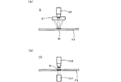
- FIG. 5 is a side view schematically showing a schematic configuration example of the first reading device 9 and the second reading device 10 (side view seen from the width direction of the polarizing film F2).
- FIG. 5A shows a schematic configuration example of the first reading device 9
- FIG. 5B shows a schematic configuration example of the second reading device 10.
- the first reading device 9 includes a UV illumination 91 that emits ultraviolet rays, and an imaging means (area sensor) 92.
- an imaging means area sensor
- the UV illumination 91 for example, one that emits ultraviolet rays having a wavelength of about 200 to 400 nm, preferably ultraviolet rays having a wavelength of about 365 nm can be used.
- the imaging means 92 for example, an area sensor with a high-speed shutter having a shutter speed (exposure time) of about 30 to 150 ⁇ sec can be used.
- the second reader 10 is arranged on one side (lower side in the example shown in FIG. 5 (b)) with respect to the surface of the polarizing film F2, and emits a parallel light beam.
- the parallel light flux emitted from the illumination 101 and irradiated on the surface of the polarizing film F2 is scattered by the second identification information N printed by laser engraving.
- the pixel area corresponding to the second identification information N becomes darker (the pixel area corresponding to the first identification information M becomes brighter as in the background), and the second identification information becomes brighter. N can be read separately from the first identification information M. Further, the second identification information N can be read separately from the unevenness of the knurled portion.
- the illumination 101 shown in FIG. 5B is replaced with the illumination that irradiates the diffused light.
- the reading device as a reading device for reading the first identification information M
- the pixel region corresponding to the first identification information M becomes darker in the captured image acquired by the imaging means 102 (corresponding to the second identification information N).
- the pixel region to be printed becomes bright as in the background), and the first identification information M can be read separately from the second identification information N. Further, the first identification information M can be read separately from the unevenness of the knurling processed portion.
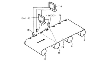
- FIG. 6 schematically illustrates a schematic configuration of an inspection system for executing the reading step S10, the second fourth step S11, and the sixth step S12 (the fourth step and the sixth step after the execution of the seventh step S9). It is a perspective view which shows. Actually, the first identification information M is printed on the protective film F1 constituting the polarizing film F2, but the illustration of the first identification information M is omitted in FIG. 6 for convenience.
- the second identification information N in the second reading device 12 having the same configuration as the second reading device 10 (see FIGS. 4 and 5B) included in the inspection system 100. To read. The read second identification information N is input to the second storage device 8.
- the second inspection device 13 (imaging means 13a and image processing means 13b) having the same configuration as the second inspection device 5 included in the inspection system 100 is roll-to-roll system by the transport roll R.
- the polarizing film F2 conveyed in (conveyed in the direction indicated by the thick line arrow in FIG. 6) is inspected to acquire the second defect information which is the defect information of the polarizing film F2.
- the acquired second defect information is input to the second arithmetic storage device 8.
- the second arithmetic storage device 8 obtains the second defect information of the polarizing film F2 acquired by the second inspection device 13 and the second identification information N read by the second reading device 12. Link and memorize. Specifically, the second arithmetic storage device 8 uses the amount of movement of the polarizing film F2 in the transport direction input from the length measuring device 14 having the same configuration as the length measuring device 3, and the second reading device 12 Which of the polarizing films F2 is between the time when the second identification information N is read and the time when the defect is detected by the second inspection device 13 (the time when the coordinates of the pixel region corresponding to the defect in the captured image are specified). It is grasped whether or not the image is moving in the transport direction, and at least the second identification information N and the coordinates of the defect based on the second identification information N are associated and stored.
- the case where two inspections (inspection by the second inspection apparatus 5 and inspection by the second inspection apparatus 13) are performed in the manufacturing process of the polarizing film F2 has been described as an example, but three or more times have been described.
- the reading step S10, the fourth step S11, and the sixth step S12 may be repeatedly executed in the second and subsequent inspections.
- the first identification information M is printed by the inkjet method. Therefore, as the present inventors have found, the first identification information M is printed on the unevenness of the nerring processed portion. Can be read separately. Further, since the first identification information M is printed by the inkjet method and the second identification information N is printed by laser engraving, according to the knowledge of the present inventors, the first identification information M and the second identification information N Even if they overlap, they can be read separately. That is, the defect information and the identification information are appropriately linked (the first defect information and the first identification information M (and thus the second identification information N) are linked, and the second defect information and the second identification information N are linked. Can be attached).
- the second identification information N is read, and the association between the second defect information and the second identification information N stored in the sixth steps S8 and S12 is used, and the first defect stored in the seventh step S9 is used.
- the link between the information and the second identification information N it is possible to punch out the product while avoiding the position of the defect generated in the state of the protective film F1 and the position of the defect generated in the state of the polarizing film F2. is there.
- the present invention is not limited to the mode in which the first identification information M is printed by the inkjet method and the second identification information N is printed by laser engraving. Either one of the first identification information M and the second identification information N is printed by the inkjet method and the other is printed by laser engraving, or one of them is printed by the inkjet method using transparent ink. Even if printing is performed and one of the other is printed by an inkjet method using colored ink, the first identification information M and the second identification information N can be read separately.
- the inspection method according to the present embodiment involves associating the first identification information M (and thus the second identification information N of the polarizing film F2) and the first defect information of the protective film F1 with the polarizing film F2. It is also possible to include an eighth step (not shown in FIG. 1) of marking the positions of defects in the polarizing film F2 based on the association of the second identification information N and the second defect information. Specifically, the second identification information N is read, and the positions of the defects included in the first defect information and the second defect information are marked by an inkjet method or marking using the same magic as described in Patent Document 1. It is also possible to apply. By including the eighth step of marking, the position of the defect is marked, so that the position of the defect can be visually specified.
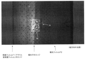
- FIG. 7 is a diagram showing a printing example of the first identification information M and the second identification information N by the inspection method according to the present embodiment.
- a protective film made of triacetylcellol (TAC) and a protective film made of acrylic are used as the protective film F1, and these protective films F1 are laminated on both sides of the polarizer. It is a polarizing film F2.
- the acrylic protective film and the TAC protective film are applied to both sides of the polarizer.
- the second identification information N is printed on the protective film side made of TAC by laser engraving.
- the captured image shown in FIG. 7 is obtained when the polarizing film F2 is illuminated by using both the UV illumination 91 provided by the first reading device 9 and the illumination 101 provided by the second reading device 10 at the same time. It is a captured image.
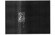
- FIG. 8 shows an example of the result of reading the first identification information M of the polarizing film F2 shown in FIG. 7 by the first reading device 9.
- the pixel area corresponding to the first identification information M becomes brighter (the pixel area corresponding to the second identification information N becomes darker as in the background. ), It can be seen that the first identification information M can be read separately from the second identification information N. Further, it can be seen that the first identification information M can be read separately from the unevenness of the knurled portion.
- FIG. 9 shows an example of the result of reading the second identification information N of the polarizing film F2 shown in FIG. 7 by the second reading device 10.
- the pixel area corresponding to the second identification information N becomes darker (the pixel area corresponding to the first identification information M becomes brighter as in the background. ), It can be seen that the second identification information N can be read separately from the first identification information M. Further, it can be seen that the second identification information N can be read separately from the unevenness of the knurled portion.
- the present invention is not limited to this. It is also possible to print the first identification information M on the part where the knurling processing portion is to be formed before forming the knurling processing portion (that is, to form the knurling processing portion after printing the first identification information M). is there.
- the case where the inspection of the polarizing film F2 is executed a plurality of times has been described as an example, but the present invention is not limited to this, and the inspection of the polarizing film F2 can be performed only once. ..
- the reading step S10, the fourth step (second time) S11, and the sixth step (second time) S12 shown in FIG. 1 are unnecessary.
- the reading step S10 is necessary.
- the present invention is not limited to this, and is executed a plurality of times as in the inspection of the polarizing film F2. It is also possible to do.
- a reading step of reading the first identification information M after the third step S4 shown in FIG. 1, a reading step of reading the first identification information M, a step of acquiring the first defect information as in the first step S2, and As in the third step S4, it is necessary to repeatedly execute the step of associating and storing the first defect information and the first identification information M.
- the first defect information and the second defect information are centrally managed based on the second identification information N of the polarizing film F2 by executing the seventh step S9.
- the state of the polarizing film F2 is obtained by punching out the product while avoiding the position of the defect, reading the second identification information N, and using the association between the second defect information and the second identification information N stored in the sixth step S8. It is also possible to punch out the product while avoiding the position of the defect generated in.
- the functional film is a protective film attached to the polarizer
- the present invention is not limited to this. It can be applied to various functional films as long as the functional film is bonded to a polarizer or an optical laminate containing the polarizer to produce a polarizing film.
- the functional film to be bonded to the polarizer include a protective film (including a film that also serves as a retardation film) exemplified in this embodiment and a retardation film.
- optical laminate containing the polarizer examples include those in which a protective film is laminated on the polarizer, and examples of the functional film to be bonded to the optical laminate include a retardation film, a reflective polarizer, an antireflection film, and ITO.
- a conductive film such as a film, for example, a window film made of polyimide or the like can be exemplified.
Landscapes
- Physics & Mathematics (AREA)
- General Physics & Mathematics (AREA)
- Health & Medical Sciences (AREA)
- Engineering & Computer Science (AREA)
- Life Sciences & Earth Sciences (AREA)
- Chemical & Material Sciences (AREA)
- Analytical Chemistry (AREA)
- Biochemistry (AREA)
- General Health & Medical Sciences (AREA)
- Textile Engineering (AREA)
- Immunology (AREA)
- Pathology (AREA)
- Optics & Photonics (AREA)
- Investigating Materials By The Use Of Optical Means Adapted For Particular Applications (AREA)
- Polarising Elements (AREA)
Applications Claiming Priority (2)
| Application Number | Priority Date | Filing Date | Title |
|---|---|---|---|
| JP2019222919 | 2019-12-10 | ||
| JP2019-222919 | 2019-12-10 |
Publications (1)
| Publication Number | Publication Date |
|---|---|
| WO2021117274A1 true WO2021117274A1 (ja) | 2021-06-17 |
Family
ID=76328945
Family Applications (2)
| Application Number | Title | Priority Date | Filing Date |
|---|---|---|---|
| PCT/JP2020/024848 Ceased WO2021117274A1 (ja) | 2019-12-10 | 2020-06-24 | 機能フィルムの検査方法、検査システム及び原反ロール |
| PCT/JP2020/045455 Ceased WO2021117671A1 (ja) | 2019-12-10 | 2020-12-07 | 機能フィルムの検査方法、検査システム及び原反ロール |
Family Applications After (1)
| Application Number | Title | Priority Date | Filing Date |
|---|---|---|---|
| PCT/JP2020/045455 Ceased WO2021117671A1 (ja) | 2019-12-10 | 2020-12-07 | 機能フィルムの検査方法、検査システム及び原反ロール |
Country Status (5)
| Country | Link |
|---|---|
| JP (1) | JP7628084B2 (https=) |
| KR (1) | KR20220113678A (https=) |
| CN (1) | CN114846321A (https=) |
| TW (2) | TW202122788A (https=) |
| WO (2) | WO2021117274A1 (https=) |
Families Citing this family (3)
| Publication number | Priority date | Publication date | Assignee | Title |
|---|---|---|---|---|
| US20230258961A1 (en) * | 2022-02-15 | 2023-08-17 | Shawn Cannon Medeiros | Disposable Prescription Stickers for Eyewear and Method of Use |
| CN115870233A (zh) * | 2022-09-30 | 2023-03-31 | 杭州利珀科技有限公司 | 偏光膜rtp前制程与rtp制程的联动方法及系统 |
| JP7838721B2 (ja) * | 2024-04-03 | 2026-04-01 | コニカミノルタ株式会社 | 情報処理システム、情報処理方法および情報処理プログラム |
Citations (6)
| Publication number | Priority date | Publication date | Assignee | Title |
|---|---|---|---|---|
| JP2003202298A (ja) * | 2002-01-07 | 2003-07-18 | Nitto Denko Corp | シート状成形体の検査結果記録方法及び検査結果記録システム及びロール状成形体及び枚葉物 |
| JP2005062165A (ja) * | 2003-07-28 | 2005-03-10 | Nitto Denko Corp | シート状製品の検査方法、検査システム、シート状製品、及び、画像表示装置 |
| US20070095451A1 (en) * | 2005-10-28 | 2007-05-03 | The Boeing Company | Systems and methods for tape flaw and splice avoidance in manufacturing |
| JP2008116438A (ja) * | 2006-10-11 | 2008-05-22 | Nitto Denko Corp | 検査データ処理装置及び検査データ処理方法 |
| JP2008175940A (ja) * | 2007-01-17 | 2008-07-31 | Sekisui Chem Co Ltd | 光学フィルムの欠陥のマーキング方法 |
| JP2017137527A (ja) * | 2016-02-02 | 2017-08-10 | 日東電工株式会社 | マーキング形成方法およびマーキング装置、ならびにフィルムの製造方法および真空成膜装置 |
Family Cites Families (10)
| Publication number | Priority date | Publication date | Assignee | Title |
|---|---|---|---|---|
| JPS5925609B2 (ja) | 1980-02-14 | 1984-06-19 | 椿本興業株式会社 | 水の除鹿装置 |
| JPH0839669A (ja) * | 1994-08-02 | 1996-02-13 | Dainippon Printing Co Ltd | 絵柄同調エンボス見当調整方法 |
| JP3899483B2 (ja) * | 2001-10-04 | 2007-03-28 | 富士フイルム株式会社 | 配向膜付き透明フィルムの製造方法 |
| KR20050013491A (ko) * | 2003-07-28 | 2005-02-04 | 닛토덴코 가부시키가이샤 | 시트형상 제품의 검사 방법 및 검사 시스템 |
| JP2005114624A (ja) * | 2003-10-09 | 2005-04-28 | Nitto Denko Corp | シート状製品の検査方法及びシート状製品の検査システム及びシート状製品及び枚葉物 |
| JP5529094B2 (ja) * | 2006-10-11 | 2014-06-25 | 日東電工株式会社 | 光学フィルムを有するシート状製品の検査データ処理装置および切断装置 |
| JP5578759B2 (ja) | 2007-08-10 | 2014-08-27 | 日東電工株式会社 | フィルム及びその製造方法 |
| JP2009244064A (ja) * | 2008-03-31 | 2009-10-22 | Sumitomo Chemical Co Ltd | 偏光フィルムの検査方法 |
| JP2009080131A (ja) * | 2008-12-01 | 2009-04-16 | Nitto Denko Corp | シート状製品の検査方法及びシート状製品の検査システム及びシート状製品及び枚葉物 |
| JP5925609B2 (ja) * | 2012-06-12 | 2016-05-25 | 日東電工株式会社 | シート状製品の検査システム及びシート状製品の検査方法 |
-
2020
- 2020-06-24 WO PCT/JP2020/024848 patent/WO2021117274A1/ja not_active Ceased
- 2020-07-20 TW TW109124439A patent/TW202122788A/zh unknown
- 2020-12-07 WO PCT/JP2020/045455 patent/WO2021117671A1/ja not_active Ceased
- 2020-12-07 CN CN202080085754.5A patent/CN114846321A/zh active Pending
- 2020-12-07 JP JP2021563946A patent/JP7628084B2/ja active Active
- 2020-12-07 KR KR1020227015641A patent/KR20220113678A/ko active Pending
- 2020-12-10 TW TW109143560A patent/TWI870515B/zh active
Patent Citations (6)
| Publication number | Priority date | Publication date | Assignee | Title |
|---|---|---|---|---|
| JP2003202298A (ja) * | 2002-01-07 | 2003-07-18 | Nitto Denko Corp | シート状成形体の検査結果記録方法及び検査結果記録システム及びロール状成形体及び枚葉物 |
| JP2005062165A (ja) * | 2003-07-28 | 2005-03-10 | Nitto Denko Corp | シート状製品の検査方法、検査システム、シート状製品、及び、画像表示装置 |
| US20070095451A1 (en) * | 2005-10-28 | 2007-05-03 | The Boeing Company | Systems and methods for tape flaw and splice avoidance in manufacturing |
| JP2008116438A (ja) * | 2006-10-11 | 2008-05-22 | Nitto Denko Corp | 検査データ処理装置及び検査データ処理方法 |
| JP2008175940A (ja) * | 2007-01-17 | 2008-07-31 | Sekisui Chem Co Ltd | 光学フィルムの欠陥のマーキング方法 |
| JP2017137527A (ja) * | 2016-02-02 | 2017-08-10 | 日東電工株式会社 | マーキング形成方法およびマーキング装置、ならびにフィルムの製造方法および真空成膜装置 |
Also Published As
| Publication number | Publication date |
|---|---|
| TW202136755A (zh) | 2021-10-01 |
| JPWO2021117671A1 (https=) | 2021-06-17 |
| TW202122788A (zh) | 2021-06-16 |
| WO2021117671A1 (ja) | 2021-06-17 |
| JP7628084B2 (ja) | 2025-02-07 |
| TWI870515B (zh) | 2025-01-21 |
| CN114846321A (zh) | 2022-08-02 |
| KR20220113678A (ko) | 2022-08-16 |
Similar Documents
| Publication | Publication Date | Title |
|---|---|---|
| KR101383934B1 (ko) | 광학 필름을 갖는 시트상 제품의 결점 검사 장치, 그 검사데이터 처리 장치, 그 절단 장치 및 그 제조 시스템 | |
| EP1914539B1 (en) | Test data processing apparatus and test data processing method | |
| JP2005114624A (ja) | シート状製品の検査方法及びシート状製品の検査システム及びシート状製品及び枚葉物 | |
| KR101375428B1 (ko) | 적층 필름의 제조 방법, 적층 필름의 결함 검출 방법, 적층필름의 결함 검출 장치, 적층 필름, 및 화상 표시 장치 | |
| JP7628084B2 (ja) | 機能フィルムの検査方法、検査システム及び原反ロール | |
| US20080193701A1 (en) | Optical film products and method for producing optical film products | |
| JP5671571B2 (ja) | 光学フィルムを有するシート状製品の検査データ処理装置および切断装置 | |
| JP5925609B2 (ja) | シート状製品の検査システム及びシート状製品の検査方法 | |
| JP7299219B2 (ja) | マーキング装置、マーキング方法、偏光板の製造方法および偏光板 | |
| JP7288989B1 (ja) | 長尺光学フィルムの検査方法 | |
| WO2021117273A1 (ja) | 長尺光学積層体の検査方法及び検査システム | |
| JP2009080131A (ja) | シート状製品の検査方法及びシート状製品の検査システム及びシート状製品及び枚葉物 |
Legal Events
| Date | Code | Title | Description |
|---|---|---|---|
| 121 | Ep: the epo has been informed by wipo that ep was designated in this application |
Ref document number: 20898798 Country of ref document: EP Kind code of ref document: A1 |
|
| NENP | Non-entry into the national phase |
Ref country code: DE |
|
| 122 | Ep: pct application non-entry in european phase |
Ref document number: 20898798 Country of ref document: EP Kind code of ref document: A1 |
|
| NENP | Non-entry into the national phase |
Ref country code: JP |