WO2021111908A1 - 半導体装置用銅ボンディングワイヤ及び半導体装置 - Google Patents
半導体装置用銅ボンディングワイヤ及び半導体装置 Download PDFInfo
- Publication number
- WO2021111908A1 WO2021111908A1 PCT/JP2020/043446 JP2020043446W WO2021111908A1 WO 2021111908 A1 WO2021111908 A1 WO 2021111908A1 JP 2020043446 W JP2020043446 W JP 2020043446W WO 2021111908 A1 WO2021111908 A1 WO 2021111908A1
- Authority
- WO
- WIPO (PCT)
- Prior art keywords
- wire
- bonding wire
- copper bonding
- semiconductor device
- less
- Prior art date
Links
- 239000010949 copper Substances 0.000 title claims abstract description 72
- 229910052802 copper Inorganic materials 0.000 title claims abstract description 68
- 239000004065 semiconductor Substances 0.000 title claims abstract description 39
- 239000013078 crystal Substances 0.000 claims abstract description 26
- 238000005259 measurement Methods 0.000 claims description 42
- 238000000034 method Methods 0.000 claims description 23
- RYGMFSIKBFXOCR-UHFFFAOYSA-N Copper Chemical compound [Cu] RYGMFSIKBFXOCR-UHFFFAOYSA-N 0.000 claims description 11
- 238000001887 electron backscatter diffraction Methods 0.000 claims 1
- 238000003860 storage Methods 0.000 abstract description 22
- 239000002019 doping agent Substances 0.000 description 16
- 238000010438 heat treatment Methods 0.000 description 16
- 238000004519 manufacturing process Methods 0.000 description 14
- 238000005491 wire drawing Methods 0.000 description 12
- 239000007789 gas Substances 0.000 description 11
- 230000000052 comparative effect Effects 0.000 description 10
- 230000008569 process Effects 0.000 description 10
- 229910052739 hydrogen Inorganic materials 0.000 description 9
- 230000004048 modification Effects 0.000 description 9
- 238000012986 modification Methods 0.000 description 9
- 230000007547 defect Effects 0.000 description 8
- UFHFLCQGNIYNRP-UHFFFAOYSA-N Hydrogen Chemical compound [H][H] UFHFLCQGNIYNRP-UHFFFAOYSA-N 0.000 description 6
- PXHVJJICTQNCMI-UHFFFAOYSA-N Nickel Chemical compound [Ni] PXHVJJICTQNCMI-UHFFFAOYSA-N 0.000 description 6
- 239000001257 hydrogen Substances 0.000 description 6
- 238000011156 evaluation Methods 0.000 description 5
- 238000012360 testing method Methods 0.000 description 5
- XKRFYHLGVUSROY-UHFFFAOYSA-N Argon Chemical compound [Ar] XKRFYHLGVUSROY-UHFFFAOYSA-N 0.000 description 4
- 230000006866 deterioration Effects 0.000 description 4
- 239000000463 material Substances 0.000 description 4
- 229910052759 nickel Inorganic materials 0.000 description 4
- 230000001590 oxidative effect Effects 0.000 description 4
- 229910052698 phosphorus Inorganic materials 0.000 description 4
- 229910052718 tin Inorganic materials 0.000 description 4
- 238000009749 continuous casting Methods 0.000 description 3
- 239000012535 impurity Substances 0.000 description 3
- 239000011261 inert gas Substances 0.000 description 3
- 238000004804 winding Methods 0.000 description 3
- IJGRMHOSHXDMSA-UHFFFAOYSA-N Atomic nitrogen Chemical compound N#N IJGRMHOSHXDMSA-UHFFFAOYSA-N 0.000 description 2
- 229910000881 Cu alloy Inorganic materials 0.000 description 2
- VEXZGXHMUGYJMC-UHFFFAOYSA-N Hydrochloric acid Chemical compound Cl VEXZGXHMUGYJMC-UHFFFAOYSA-N 0.000 description 2
- 229910045601 alloy Inorganic materials 0.000 description 2
- 239000000956 alloy Substances 0.000 description 2
- 229910052786 argon Inorganic materials 0.000 description 2
- QVGXLLKOCUKJST-UHFFFAOYSA-N atomic oxygen Chemical compound [O] QVGXLLKOCUKJST-UHFFFAOYSA-N 0.000 description 2
- 230000004888 barrier function Effects 0.000 description 2
- 229910001873 dinitrogen Inorganic materials 0.000 description 2
- 230000007613 environmental effect Effects 0.000 description 2
- 239000010931 gold Substances 0.000 description 2
- 230000008018 melting Effects 0.000 description 2
- 238000002844 melting Methods 0.000 description 2
- 230000003287 optical effect Effects 0.000 description 2
- 239000001301 oxygen Substances 0.000 description 2
- 229910052760 oxygen Inorganic materials 0.000 description 2
- 238000007747 plating Methods 0.000 description 2
- 229910052761 rare earth metal Inorganic materials 0.000 description 2
- 239000002994 raw material Substances 0.000 description 2
- 229910052710 silicon Inorganic materials 0.000 description 2
- 238000010998 test method Methods 0.000 description 2
- OAICVXFJPJFONN-UHFFFAOYSA-N Phosphorus Chemical compound [P] OAICVXFJPJFONN-UHFFFAOYSA-N 0.000 description 1
- XUIMIQQOPSSXEZ-UHFFFAOYSA-N Silicon Chemical compound [Si] XUIMIQQOPSSXEZ-UHFFFAOYSA-N 0.000 description 1
- ATJFFYVFTNAWJD-UHFFFAOYSA-N Tin Chemical compound [Sn] ATJFFYVFTNAWJD-UHFFFAOYSA-N 0.000 description 1
- 230000001133 acceleration Effects 0.000 description 1
- 239000007864 aqueous solution Substances 0.000 description 1
- 238000000151 deposition Methods 0.000 description 1
- 229910003460 diamond Inorganic materials 0.000 description 1
- 239000010432 diamond Substances 0.000 description 1
- 238000001035 drying Methods 0.000 description 1
- 230000000694 effects Effects 0.000 description 1
- 239000010408 film Substances 0.000 description 1
- PCHJSUWPFVWCPO-UHFFFAOYSA-N gold Chemical compound [Au] PCHJSUWPFVWCPO-UHFFFAOYSA-N 0.000 description 1
- 229910052737 gold Inorganic materials 0.000 description 1
- 239000001307 helium Substances 0.000 description 1
- 229910052734 helium Inorganic materials 0.000 description 1
- SWQJXJOGLNCZEY-UHFFFAOYSA-N helium atom Chemical compound [He] SWQJXJOGLNCZEY-UHFFFAOYSA-N 0.000 description 1
- 230000006872 improvement Effects 0.000 description 1
- 238000005304 joining Methods 0.000 description 1
- 239000007788 liquid Substances 0.000 description 1
- 230000007774 longterm Effects 0.000 description 1
- 230000001050 lubricating effect Effects 0.000 description 1
- 239000011574 phosphorus Substances 0.000 description 1
- 238000005554 pickling Methods 0.000 description 1
- 238000010248 power generation Methods 0.000 description 1
- 238000012545 processing Methods 0.000 description 1
- 230000009467 reduction Effects 0.000 description 1
- 229910052706 scandium Inorganic materials 0.000 description 1
- SIXSYDAISGFNSX-UHFFFAOYSA-N scandium atom Chemical compound [Sc] SIXSYDAISGFNSX-UHFFFAOYSA-N 0.000 description 1
- 239000010703 silicon Substances 0.000 description 1
- 239000000758 substrate Substances 0.000 description 1
- 238000010408 sweeping Methods 0.000 description 1
- 230000008685 targeting Effects 0.000 description 1
- JBQYATWDVHIOAR-UHFFFAOYSA-N tellanylidenegermanium Chemical compound [Te]=[Ge] JBQYATWDVHIOAR-UHFFFAOYSA-N 0.000 description 1
- 238000007736 thin film deposition technique Methods 0.000 description 1
- 239000011135 tin Substances 0.000 description 1
- 229910052727 yttrium Inorganic materials 0.000 description 1
- VWQVUPCCIRVNHF-UHFFFAOYSA-N yttrium atom Chemical compound [Y] VWQVUPCCIRVNHF-UHFFFAOYSA-N 0.000 description 1
- 229910052725 zinc Inorganic materials 0.000 description 1
- 239000011701 zinc Substances 0.000 description 1
Classifications
-
- B—PERFORMING OPERATIONS; TRANSPORTING
- B23—MACHINE TOOLS; METAL-WORKING NOT OTHERWISE PROVIDED FOR
- B23K—SOLDERING OR UNSOLDERING; WELDING; CLADDING OR PLATING BY SOLDERING OR WELDING; CUTTING BY APPLYING HEAT LOCALLY, e.g. FLAME CUTTING; WORKING BY LASER BEAM
- B23K35/00—Rods, electrodes, materials, or media, for use in soldering, welding, or cutting
- B23K35/22—Rods, electrodes, materials, or media, for use in soldering, welding, or cutting characterised by the composition or nature of the material
- B23K35/24—Selection of soldering or welding materials proper
- B23K35/30—Selection of soldering or welding materials proper with the principal constituent melting at less than 1550 degrees C
- B23K35/302—Cu as the principal constituent
-
- H—ELECTRICITY
- H01—ELECTRIC ELEMENTS
- H01L—SEMICONDUCTOR DEVICES NOT COVERED BY CLASS H10
- H01L24/00—Arrangements for connecting or disconnecting semiconductor or solid-state bodies; Methods or apparatus related thereto
- H01L24/01—Means for bonding being attached to, or being formed on, the surface to be connected, e.g. chip-to-package, die-attach, "first-level" interconnects; Manufacturing methods related thereto
- H01L24/42—Wire connectors; Manufacturing methods related thereto
- H01L24/44—Structure, shape, material or disposition of the wire connectors prior to the connecting process
- H01L24/45—Structure, shape, material or disposition of the wire connectors prior to the connecting process of an individual wire connector
-
- B—PERFORMING OPERATIONS; TRANSPORTING
- B23—MACHINE TOOLS; METAL-WORKING NOT OTHERWISE PROVIDED FOR
- B23K—SOLDERING OR UNSOLDERING; WELDING; CLADDING OR PLATING BY SOLDERING OR WELDING; CUTTING BY APPLYING HEAT LOCALLY, e.g. FLAME CUTTING; WORKING BY LASER BEAM
- B23K35/00—Rods, electrodes, materials, or media, for use in soldering, welding, or cutting
- B23K35/02—Rods, electrodes, materials, or media, for use in soldering, welding, or cutting characterised by mechanical features, e.g. shape
- B23K35/0255—Rods, electrodes, materials, or media, for use in soldering, welding, or cutting characterised by mechanical features, e.g. shape for use in welding
- B23K35/0261—Rods, electrodes, wires
-
- C—CHEMISTRY; METALLURGY
- C22—METALLURGY; FERROUS OR NON-FERROUS ALLOYS; TREATMENT OF ALLOYS OR NON-FERROUS METALS
- C22C—ALLOYS
- C22C9/00—Alloys based on copper
-
- C—CHEMISTRY; METALLURGY
- C22—METALLURGY; FERROUS OR NON-FERROUS ALLOYS; TREATMENT OF ALLOYS OR NON-FERROUS METALS
- C22F—CHANGING THE PHYSICAL STRUCTURE OF NON-FERROUS METALS AND NON-FERROUS ALLOYS
- C22F1/00—Changing the physical structure of non-ferrous metals or alloys by heat treatment or by hot or cold working
- C22F1/08—Changing the physical structure of non-ferrous metals or alloys by heat treatment or by hot or cold working of copper or alloys based thereon
-
- H—ELECTRICITY
- H01—ELECTRIC ELEMENTS
- H01L—SEMICONDUCTOR DEVICES NOT COVERED BY CLASS H10
- H01L21/00—Processes or apparatus adapted for the manufacture or treatment of semiconductor or solid state devices or of parts thereof
- H01L21/02—Manufacture or treatment of semiconductor devices or of parts thereof
- H01L21/04—Manufacture or treatment of semiconductor devices or of parts thereof the devices having potential barriers, e.g. a PN junction, depletion layer or carrier concentration layer
- H01L21/50—Assembly of semiconductor devices using processes or apparatus not provided for in a single one of the subgroups H01L21/06 - H01L21/326, e.g. sealing of a cap to a base of a container
-
- H—ELECTRICITY
- H01—ELECTRIC ELEMENTS
- H01L—SEMICONDUCTOR DEVICES NOT COVERED BY CLASS H10
- H01L24/00—Arrangements for connecting or disconnecting semiconductor or solid-state bodies; Methods or apparatus related thereto
- H01L24/01—Means for bonding being attached to, or being formed on, the surface to be connected, e.g. chip-to-package, die-attach, "first-level" interconnects; Manufacturing methods related thereto
- H01L24/42—Wire connectors; Manufacturing methods related thereto
- H01L24/43—Manufacturing methods
-
- H—ELECTRICITY
- H01—ELECTRIC ELEMENTS
- H01L—SEMICONDUCTOR DEVICES NOT COVERED BY CLASS H10
- H01L2224/00—Indexing scheme for arrangements for connecting or disconnecting semiconductor or solid-state bodies and methods related thereto as covered by H01L24/00
- H01L2224/01—Means for bonding being attached to, or being formed on, the surface to be connected, e.g. chip-to-package, die-attach, "first-level" interconnects; Manufacturing methods related thereto
- H01L2224/42—Wire connectors; Manufacturing methods related thereto
- H01L2224/44—Structure, shape, material or disposition of the wire connectors prior to the connecting process
- H01L2224/45—Structure, shape, material or disposition of the wire connectors prior to the connecting process of an individual wire connector
- H01L2224/45001—Core members of the connector
- H01L2224/4501—Shape
- H01L2224/45012—Cross-sectional shape
- H01L2224/45015—Cross-sectional shape being circular
-
- H—ELECTRICITY
- H01—ELECTRIC ELEMENTS
- H01L—SEMICONDUCTOR DEVICES NOT COVERED BY CLASS H10
- H01L2224/00—Indexing scheme for arrangements for connecting or disconnecting semiconductor or solid-state bodies and methods related thereto as covered by H01L24/00
- H01L2224/01—Means for bonding being attached to, or being formed on, the surface to be connected, e.g. chip-to-package, die-attach, "first-level" interconnects; Manufacturing methods related thereto
- H01L2224/42—Wire connectors; Manufacturing methods related thereto
- H01L2224/44—Structure, shape, material or disposition of the wire connectors prior to the connecting process
- H01L2224/45—Structure, shape, material or disposition of the wire connectors prior to the connecting process of an individual wire connector
- H01L2224/45001—Core members of the connector
- H01L2224/45099—Material
- H01L2224/451—Material with a principal constituent of the material being a metal or a metalloid, e.g. boron (B), silicon (Si), germanium (Ge), arsenic (As), antimony (Sb), tellurium (Te) and polonium (Po), and alloys thereof
- H01L2224/45138—Material with a principal constituent of the material being a metal or a metalloid, e.g. boron (B), silicon (Si), germanium (Ge), arsenic (As), antimony (Sb), tellurium (Te) and polonium (Po), and alloys thereof the principal constituent melting at a temperature of greater than or equal to 950°C and less than 1550°C
- H01L2224/45147—Copper (Cu) as principal constituent
-
- H—ELECTRICITY
- H01—ELECTRIC ELEMENTS
- H01L—SEMICONDUCTOR DEVICES NOT COVERED BY CLASS H10
- H01L2924/00—Indexing scheme for arrangements or methods for connecting or disconnecting semiconductor or solid-state bodies as covered by H01L24/00
- H01L2924/012—Semiconductor purity grades
- H01L2924/01203—3N purity grades, i.e. 99.9%
-
- H—ELECTRICITY
- H01—ELECTRIC ELEMENTS
- H01L—SEMICONDUCTOR DEVICES NOT COVERED BY CLASS H10
- H01L2924/00—Indexing scheme for arrangements or methods for connecting or disconnecting semiconductor or solid-state bodies as covered by H01L24/00
- H01L2924/20—Parameters
- H01L2924/207—Diameter ranges
- H01L2924/20751—Diameter ranges larger or equal to 10 microns less than 20 microns
-
- H—ELECTRICITY
- H01—ELECTRIC ELEMENTS
- H01L—SEMICONDUCTOR DEVICES NOT COVERED BY CLASS H10
- H01L2924/00—Indexing scheme for arrangements or methods for connecting or disconnecting semiconductor or solid-state bodies as covered by H01L24/00
- H01L2924/20—Parameters
- H01L2924/207—Diameter ranges
- H01L2924/20752—Diameter ranges larger or equal to 20 microns less than 30 microns
-
- H—ELECTRICITY
- H01—ELECTRIC ELEMENTS
- H01L—SEMICONDUCTOR DEVICES NOT COVERED BY CLASS H10
- H01L2924/00—Indexing scheme for arrangements or methods for connecting or disconnecting semiconductor or solid-state bodies as covered by H01L24/00
- H01L2924/20—Parameters
- H01L2924/207—Diameter ranges
- H01L2924/20753—Diameter ranges larger or equal to 30 microns less than 40 microns
-
- H—ELECTRICITY
- H01—ELECTRIC ELEMENTS
- H01L—SEMICONDUCTOR DEVICES NOT COVERED BY CLASS H10
- H01L2924/00—Indexing scheme for arrangements or methods for connecting or disconnecting semiconductor or solid-state bodies as covered by H01L24/00
- H01L2924/20—Parameters
- H01L2924/207—Diameter ranges
- H01L2924/20754—Diameter ranges larger or equal to 40 microns less than 50 microns
-
- H—ELECTRICITY
- H01—ELECTRIC ELEMENTS
- H01L—SEMICONDUCTOR DEVICES NOT COVERED BY CLASS H10
- H01L2924/00—Indexing scheme for arrangements or methods for connecting or disconnecting semiconductor or solid-state bodies as covered by H01L24/00
- H01L2924/20—Parameters
- H01L2924/207—Diameter ranges
- H01L2924/20755—Diameter ranges larger or equal to 50 microns less than 60 microns
-
- H—ELECTRICITY
- H01—ELECTRIC ELEMENTS
- H01L—SEMICONDUCTOR DEVICES NOT COVERED BY CLASS H10
- H01L2924/00—Indexing scheme for arrangements or methods for connecting or disconnecting semiconductor or solid-state bodies as covered by H01L24/00
- H01L2924/20—Parameters
- H01L2924/207—Diameter ranges
- H01L2924/20756—Diameter ranges larger or equal to 60 microns less than 70 microns
-
- H—ELECTRICITY
- H01—ELECTRIC ELEMENTS
- H01L—SEMICONDUCTOR DEVICES NOT COVERED BY CLASS H10
- H01L2924/00—Indexing scheme for arrangements or methods for connecting or disconnecting semiconductor or solid-state bodies as covered by H01L24/00
- H01L2924/20—Parameters
- H01L2924/207—Diameter ranges
- H01L2924/20757—Diameter ranges larger or equal to 70 microns less than 80 microns
-
- H—ELECTRICITY
- H01—ELECTRIC ELEMENTS
- H01L—SEMICONDUCTOR DEVICES NOT COVERED BY CLASS H10
- H01L2924/00—Indexing scheme for arrangements or methods for connecting or disconnecting semiconductor or solid-state bodies as covered by H01L24/00
- H01L2924/20—Parameters
- H01L2924/207—Diameter ranges
- H01L2924/20758—Diameter ranges larger or equal to 80 microns less than 90 microns
-
- H—ELECTRICITY
- H01—ELECTRIC ELEMENTS
- H01L—SEMICONDUCTOR DEVICES NOT COVERED BY CLASS H10
- H01L2924/00—Indexing scheme for arrangements or methods for connecting or disconnecting semiconductor or solid-state bodies as covered by H01L24/00
- H01L2924/20—Parameters
- H01L2924/207—Diameter ranges
- H01L2924/20759—Diameter ranges larger or equal to 90 microns less than 100 microns
-
- H—ELECTRICITY
- H01—ELECTRIC ELEMENTS
- H01L—SEMICONDUCTOR DEVICES NOT COVERED BY CLASS H10
- H01L2924/00—Indexing scheme for arrangements or methods for connecting or disconnecting semiconductor or solid-state bodies as covered by H01L24/00
- H01L2924/20—Parameters
- H01L2924/207—Diameter ranges
- H01L2924/2076—Diameter ranges equal to or larger than 100 microns
Definitions
- the present invention relates to a copper bonding wire for a semiconductor device. Furthermore, the present invention relates to a semiconductor device including the copper bonding wire.
- the copper bonding wire is wound on a spool to form a wound body, and then the wound body is sealed with a barrier bag that blocks oxygen, moisture, etc. before shipping. Then, the barrier bag is opened immediately before being used for the connection between the electrodes in the manufacture of the semiconductor device. Since the surface of copper bonding wire is easily oxidized due to the influence of oxygen and moisture in the atmosphere and the connectivity is easily deteriorated, the storage period after opening is generally set to one week.
- the wire length (winding length) in the wound body is limited to be short, and in that case, the frequency of replacement of the wound body increases, and it is necessary to stop the line each time, resulting in a decrease in production efficiency. Is inevitable. Therefore, it is required to improve the storage life of copper bonding wires in the atmosphere.
- An object of the present invention is to provide a copper bonding wire having an improved storage life in the atmosphere.
- the boundary where the grain boundary density on the surface is measured by the EBSD method at a measurement point interval of 0.06 ⁇ m or more and 0.6 ⁇ m or less and the orientation difference between adjacent measurement points is 15 ° or more is regarded as a crystal grain boundary.
- the crystal grain boundary density on the surface is positioned so that the center of the width of the wire in the direction perpendicular to the longitudinal axis of the wire is the center of the width of the measurement surface, and the width of the measurement surface is 20% of the wire diameter.
- the copper bonding wire according to [2] which is measured under the condition that the length of the measuring surface is 40% or more and the length of the measuring surface is 5 times the width of the measuring surface.
- [5] The copper bonding wire according to any one of [1] to [4], wherein the wire diameter is 15 ⁇ m or more and 300 ⁇ m or less.
- [6] The copper bonding wire according to any one of [1] to [5], which has a breaking strength of 145 MPa or more.
- [7] A semiconductor device including the copper bonding wire according to any one of [1] to [6].
- the copper bonding wire for a semiconductor device of the present invention is characterized in that the grain boundary density on the surface is 0.6 ( ⁇ m / ⁇ m 2 ) or more and 1.6 ( ⁇ m / ⁇ m 2 ) or less.
- the average crystal grain size is known as an index showing the crystal structure of the bonding wire, and efforts have been made to adjust the average crystal grain size within a certain range in order to realize the desired wire properties.
- a technique for adding a certain amount of dopant and adjusting the average crystal grain size of the wire within a certain range for example, Japanese Patent Application Laid-Open No. 2018-503743, International Pamphlet WO2017). / 221770, etc.
- the present inventors investigated the influence of the average crystal grain size and the like of the copper bonding wire in relation to the storage life of the copper bonding wire in the atmosphere. As a result, it was confirmed that the storage life in the atmosphere and the average crystal grain size of the wire do not necessarily correlate with each other.
- the present inventors have found that the grain boundary density on the wire surface correlates well with the storage life in the atmosphere in the process of diligently studying to improve the storage life of the copper bonding wire in the atmosphere. It has reached.
- the above-mentioned average crystal grain size may be used as an index showing bulk characteristics such as strength characteristics of polycrystalline materials and bonding strength of bonding materials, as represented by Hall-petch's empirical rule.
- the average crystal grain size and the grain boundary density may be used interchangeably.
- the properties do not necessarily correlate with the average grain size, while the properties and grain boundary densities are good. It was found to correlate.
- the grain boundary density means the total length ( ⁇ m) of the crystal grain boundaries existing per unit area ( ⁇ m 2), and indicates how many grain boundaries exist per unit area. It is an index.
- the upper limit of the crystal grain boundary density on the surface is 1.6 ( ⁇ m / ⁇ m 2 ) or less, preferably 1.55 ( ⁇ m / ⁇ m). 2 ) or less, more preferably 1.5 ( ⁇ m / ⁇ m 2 ) or less, 1.45 ( ⁇ m / ⁇ m 2 ) or less, or 1.4 ( ⁇ m / ⁇ m 2 ) or less.
- the lower limit of the crystal grain boundary density on the surface is 0.6 ( ⁇ m / ⁇ m 2 ) or more from the viewpoint of realizing a copper bonding wire that exhibits sufficient breaking strength and can stably form a desired loop shape. Yes, preferably 0.65 ( ⁇ m / ⁇ m 2 ) or more, 0.7 ( ⁇ m / ⁇ m 2 ) or more, 0.75 ( ⁇ m / ⁇ m 2 ) or more, 0.8 ( ⁇ m / ⁇ m 2 ) or more, or 0 It is .85 ( ⁇ m / ⁇ m 2 ) or more.
- the grain boundary density on the surface is measured and calculated by the EBSD (Electron Backscattered Diffraction) method with the wire surface as the observation surface.
- the grain boundaries are measured at a measurement point interval of 0.06 ⁇ m or more and 0.6 ⁇ m or less by the EBSD method, and the boundary where the orientation difference between adjacent measurement points is 15 ° or more is regarded as the grain boundary.
- the total length of the crystal grain boundaries is the boundary where the orientation difference between adjacent measurement points is 15 ° or more in the histogram obtained by the EBSD analysis software AZtec HKL (manufactured by Oxford Instruments Co., Ltd.). Is calculated by multiplying the frequency by the measurement point interval.
- the position and dimensions of the measurement surface are determined as follows.
- the width of the measurement surface means the dimension of the measurement surface in the direction perpendicular to the wire longitudinal axis
- the length of the measurement surface means the dimension of the measurement surface in the direction of the wire longitudinal axis.
- the copper bonding wire used for measurement is linearly fixed to the sample holder.
- the center of the width of the wire in the direction perpendicular to the longitudinal axis of the wire (that is, the center of the width of the wire when the surface of the wire is viewed in the direction perpendicular to the longitudinal axis of the wire) is then positioned to be the center of the width of the measurement surface.
- the measurement surface is determined so that the width of the measurement surface is 20% or more and 40% or less of the wire diameter.
- the copper bonding wire of the present invention is made of copper or a copper alloy.
- the content of copper in the wire is preferably 99.9% by mass or more, more preferably 99.99% by mass or more, or 99.999% by mass or more from the viewpoint of further enjoying the effects of the present invention.
- any dopant known to be able to impart environmental resistance may be added to the copper bonding wire of the present invention.
- dopants include rare earth elements such as scandium (Sc) and yttrium (Y), phosphorus (P), tin (Sn), zinc (Zn), nickel (Ni) and silicon (Si).
- the content of the dopant may be 1 mass ppm or more, 3 mass ppm or more, 5 mass ppm or more, 10 mass ppm or more, and the upper limit of the content is 500 mass ppm or less, 400 mass ppm or less, 300 mass ppm or less. Alternatively, it may be 200 mass ppm or less.
- the copper bonding wire of the present invention contains 1 to 500 mass ppm of one or more elements selected from the group consisting of rare earth elements, P, Sn, Zn, Ni and Si. Even when such a dopant is not added or the amount added is extremely small (for example, 100 mass ppm or less, 50 mass ppm or less, 30 mass ppm or less, etc.), the copper bonding wire of the present invention can be used in the atmosphere. It can exhibit a good storage life.
- the copper bonding wire of the present invention comprises copper and unavoidable impurities.
- the diameter of the copper bonding wire of the present invention is not particularly limited and may be appropriately determined according to a specific purpose, but is preferably 15 ⁇ m or more, 18 ⁇ m or more, 20 ⁇ m or more, or the like.
- the upper limit of the diameter is not particularly limited, and may be, for example, 300 ⁇ m or less, 250 ⁇ m or less, 200 ⁇ m or less, 150 ⁇ m or less, 100 ⁇ m or less, 80 ⁇ m or less, 60 ⁇ m or less, or 50 ⁇ m or less. Therefore, in one embodiment, the diameter of the copper bonding wire of the present invention is 15 ⁇ m or more and 300 ⁇ m or less.
- Raw copper having a purity of 3N to 6N (99.9 to 99.9999% by mass) is processed into a large diameter by continuous casting, and then thinned to the final wire diameter by wire drawing.
- a copper alloy containing a required concentration of the dopant may be used as a raw material.
- a high-purity dopant component may be directly added, or a mother alloy containing about 1% of the dopant component may be used.
- it may be contained by depositing a dopant component on the surface of the wire in the middle of the wire manufacturing process. In this case, it may be incorporated anywhere in the wire manufacturing process, or may be incorporated in a plurality of processes.
- the adhesion method can be selected from (1) application of an aqueous solution ⁇ drying ⁇ heat treatment, (2) plating method (wet type), and (3) thin film deposition method (dry method).
- the wire drawing process can be performed using a continuous wire drawing device that can set a plurality of diamond-coated dies. If necessary, heat treatment may be performed in the middle of the wire drawing process.
- the surface modification heat treatment is preferably performed at a high temperature for a short time from the viewpoint of realizing a copper bonding wire having a surface crystal grain boundary density within a predetermined range.
- the time of the surface modification heat treatment is preferably set to several seconds at the longest (for example, 7 seconds or less, 5 seconds or less, 4 seconds or less, etc.).
- a hydrogen-containing inert gas is suitable as the atmosphere gas for the surface modification heat treatment.
- hydrogen-containing helium gas, hydrogen-containing nitrogen gas, and hydrogen-containing argon. Gas can be mentioned.
- the hydrogen concentration in the hydrogen-containing inert gas may be, for example, in the range of 1 to 20%.
- the atmospheric gas on the surface modification heat treatment is forming gas (5% H 2 -N 2) .
- an inert gas such as nitrogen gas or argon gas may be used as the atmospheric gas under strict control of the temperature and time during the heat treatment.
- the copper bonding wire of the present invention has an excellent storage life in the atmosphere because the grain boundary density on the surface is within a predetermined range.
- the copper bonding wire of the present invention also exhibits good strength due to the crystal structure inside the wire.
- the breaking strength of the copper bonding wire of the present invention is preferably 145 MPa or more, more preferably 150 MPa or more, 155 MPa or more, or 160 MPa or more.
- the upper limit of the breaking strength is not particularly limited, but may be usually 250 MPa or less, 200 MPa or less, or the like.
- the breaking strength of the copper bonding wire can be measured by the method described in [Breaking strength] described later.
- the wire winding body can be formed by winding the wire on a spool. Since the copper bonding wire of the present invention has an excellent storage life in the atmosphere, it is unlikely to cause a problem of oxidative deterioration even when it is wound for a long time, and it contributes significantly to the improvement of the production efficiency of the semiconductor device. is there.
- the copper bonding wire of the present invention can be used to connect an electrode on a semiconductor chip with an electrode on a lead frame or a circuit board in the manufacture of a semiconductor device.
- the first connection (1st bonding) with the electrode on the semiconductor chip may be ball bonding or wedge bonding.
- ball bonding the tip of a wire is heated and melted by arc heat input to form a ball (FAB: Free Air Ball) by surface tension, and then the ball portion is pressure-bonded onto the electrode of the heated semiconductor element.
- FAB Free Air Ball
- wedge bonding the wire portion is pressure-bonded onto the electrode by applying heat, ultrasonic waves, or pressure without forming a ball.
- the copper bonding wire of the present invention having a surface crystal grain boundary density within a predetermined range has an excellent storage life in the atmosphere even if no dopant is added or the amount of the dopant added is extremely small. Hardening can be suppressed, and chip damage during ball bonding can be suppressed. Further, the copper bonding wire of the present invention having an excellent storage life in the atmosphere can suppress connection failure due to oxidative deterioration even after long-term storage in the atmosphere, and can secure a wide process window.
- the second connection (2nd bonding) with the electrode on the lead frame or the circuit board can be wedge bonding, and by using the copper bonding wire of the present invention, a wide process window can be secured as described above.
- a semiconductor device can be manufactured by connecting an electrode on a semiconductor chip with an electrode on a lead frame or a circuit board using the copper bonding wire for a semiconductor device of the present invention.
- the semiconductor device of the present invention includes a circuit board, a semiconductor chip, and a copper bonding wire for conducting the circuit board and the semiconductor chip, and the copper bonding wire is the copper bonding wire of the present invention. It is characterized by.
- the circuit board and the semiconductor chip are not particularly limited, and known circuit boards and semiconductor chips that can be used to form the semiconductor device may be used.
- a lead frame may be used instead of the circuit board.
- the semiconductor device may be configured to include a lead frame and a semiconductor chip mounted on the lead frame.
- Semiconductor devices are used in electrical products (for example, computers, mobile phones, digital cameras, televisions, air conditioners, solar power generation systems, etc.) and vehicles (for example, motorcycles, automobiles, trains, ships, aircraft, etc.).
- electrical products for example, computers, mobile phones, digital cameras, televisions, air conditioners, solar power generation systems, etc.
- vehicles for example, motorcycles, automobiles, trains, ships, aircraft, etc.
- power semiconductor devices power semiconductor devices
- Example 2 First, a method for producing a sample will be described.
- Cu used as a raw material for the wire had a purity of 99.9% by mass (3N) or more to 99.999% by mass (5N) or more, and the balance was composed of unavoidable impurities. Copper having such a predetermined purity was produced by continuous casting so as to have a wire diameter of several mm.
- Sn, P, and Ni When the dopants Sn, P, and Ni are added, Sn, P, and Ni have a purity of 99% by mass or more and the balance is composed of unavoidable impurities, or a mother alloy in which a dopant is mixed in Cu at a high concentration. Using.
- the wire drawing is performed with pickling treatment with hydrochloric acid or the like in order to remove the oxide film on the wire surface, and then a plurality of dies having a surface reduction rate in the range of 10 to 26% (of which more than half of the dies are reduced).
- Wire drawing was performed using a surface ratio of 18% or more), and the wire was processed to the final wire diameter. If necessary, heat treatment at 200 to 600 ° C. for 5 to 15 seconds was performed 0 to 2 times during the wire drawing process.
- the final wire diameters were 20 ⁇ m (Examples 1 to 11, 15 to 17 and Comparative Examples 1 to 4, 7) and 30 ⁇ m (Examples 12 to 14 and Comparative Examples 5 to 6).
- surface modification heat treatment was performed at 540 to 820 ° C. for several seconds at the longest.
- Comparative Examples 1, 4 and 5 the heat treatment was performed at 500 to 650 ° C.
- Test / evaluation method The test / evaluation method will be described below.
- the total length of the obtained crystal grain boundaries a ([mu] m) is divided by the measurement area ( ⁇ m 2), was calculated grain boundary density of the surface ( ⁇ m / ⁇ m 2).
- the measurement by the EBSD method was carried out on three measurement surfaces separated from each other by 1 mm or more in the longitudinal direction of the wire, and the average value thereof was adopted.
- breaking strength of the wire was measured by using an Instron tensile tester under the conditions of a distance between gauge points of 100 mm, a tensile speed of 10 mm / min, and a load cell rated load of 5 N. In this test, the value obtained by dividing the broken load of the wire by the initial (before the test) wire cross-sectional area was defined as the breaking load. The measurement was carried out 5 times, and the average value was adopted as the breaking strength of the sample.
- Evaluation criteria ⁇ : 33 conditions or more ⁇ : 30 to 32 conditions ⁇ : 26 to 29 conditions ⁇ : 25 conditions or less
- loop shape stability The loop shape stability (reproducibility of the loop profile) was evaluated from the standard deviation of the height by connecting 40 trapezoidal loops so that the wire length was 3 mm and the loop height was 250 ⁇ m. An optical microscope was used for height measurement, and the positions were measured at two points, one near the top of the loop and the other at the center of the loop. If the standard deviation of the loop height is 1 ⁇ 2 or more of the wire diameter, it is judged that the variation is large, and if it is less than 1 ⁇ 2, the variation is small and good. Then, the evaluation was made according to the criteria shown in Table 3.
- Table 4 shows the evaluation results of Examples and Comparative Examples.
Landscapes
- Engineering & Computer Science (AREA)
- Chemical & Material Sciences (AREA)
- Mechanical Engineering (AREA)
- Computer Hardware Design (AREA)
- Microelectronics & Electronic Packaging (AREA)
- Power Engineering (AREA)
- Organic Chemistry (AREA)
- Metallurgy (AREA)
- Materials Engineering (AREA)
- Physics & Mathematics (AREA)
- Manufacturing & Machinery (AREA)
- Thermal Sciences (AREA)
- Crystallography & Structural Chemistry (AREA)
- Condensed Matter Physics & Semiconductors (AREA)
- General Physics & Mathematics (AREA)
- Wire Bonding (AREA)
Abstract
大気中での保管寿命が向上した銅ボンディングワイヤを提供する。すなわち、表面の結晶粒界密度が0.6(μm/μm2)以上1.6(μm/μm2)以下である、半導体装置用銅ボンディングワイヤを提供する。
Description
本発明は、半導体装置用銅ボンディングワイヤに関する。さらには、該銅ボンディングワイヤを含む半導体装置に関する。
半導体装置では、半導体チップ上に形成された電極と、リードフレームや基板上の電極との間をボンディングワイヤによって接続している。これまでボンディングワイヤの材料は金(Au)が主流であったが、LSI用途を中心に銅(Cu)への代替が進んでおり(例えば、特許文献1~3)、また、パワー半導体用途においても、熱伝導率や溶断電流の高さから、高効率で信頼性も高いCuへの代替が期待されている。
銅ボンディングワイヤは、スプールに巻き取られ巻装体とされた後、該巻装体を、酸素や水分等を遮断するバリア袋により密封して出荷される。そして、半導体装置の製造において電極間の接続に供される直前にバリア袋が開封される。銅ボンディングワイヤは、大気中の酸素や水分等の影響により表面酸化が進行し接続性が劣化し易いことから、開封後の保管期限は一般的に一週間とされている。
しかし、開封後一週間では使い切れずに廃棄されてしまう場合がある。また、巻装体におけるワイヤ長さ(巻き長さ)が短く制限されてしまい、その場合には、巻装体の交換頻度が増し、その都度ラインを停止する必要があるなど、生産効率の低下は避けられない。したがって、銅ボンディングワイヤについて大気中での保管寿命を向上させることが求められている。
本発明は、大気中での保管寿命が向上した銅ボンディングワイヤを提供することを課題とする。
本発明者らは、上記課題につき鋭意検討した結果、下記構成を有する銅ボンディングワイヤによって上記課題を解決できることを見出し、斯かる知見に基づいて更に検討を重ねることによって本発明を完成した。
すなわち、本発明は以下の内容を含む。
[1] 表面の結晶粒界密度が0.6(μm/μm2)以上1.6(μm/μm2)以下である、半導体装置用銅ボンディングワイヤ。
[2] 表面の結晶粒界密度が、EBSD法により測定点間隔0.06μm以上0.6μm以下で測定し、隣接する測定点間の方位差が15°以上である境界を結晶粒界とみなした場合の結晶粒界の総長さ(μm)を測定面積(μm2)で除して算出される、[1]に記載の銅ボンディングワイヤ。
[3] 表面の結晶粒界密度が、ワイヤ長手軸に垂直な方向におけるワイヤの幅の中心が測定面の幅の中心となるように位置決めし、かつ、測定面の幅がワイヤ直径の20%以上40%以下、測定面の長さが測定面の幅の5倍となる条件にて測定される、[2]に記載の銅ボンディングワイヤ。
[4] 純度99.9質量%以上の銅からなる、[1]~[3]の何れかに記載の銅ボンディングワイヤ。
[5] ワイヤ直径が15μm以上300μm以下である、[1]~[4]の何れかに記載の銅ボンディングワイヤ。
[6] 破断強度が145MPa以上である、[1]~[5]の何れかに記載の銅ボンディングワイヤ。
[7] [1]~[6]の何れかに記載の銅ボンディングワイヤを含む半導体装置。
本発明によれば、大気中での保管寿命が向上した銅ボンディングワイヤを提供することができる。
以下、本発明をその好適な実施形態に即して詳細に説明する。
[半導体装置用銅ボンディングワイヤ]
本発明の半導体装置用銅ボンディングワイヤは、表面の結晶粒界密度が0.6(μm/μm2)以上1.6(μm/μm2)以下であることを特徴とする。
本発明の半導体装置用銅ボンディングワイヤは、表面の結晶粒界密度が0.6(μm/μm2)以上1.6(μm/μm2)以下であることを特徴とする。
ボンディングワイヤの結晶組織を表す指標としては平均結晶粒径が知られており、所期のワイヤ性状を実現すべく、斯かる平均結晶粒径を一定範囲に調整する取り組みが従前よりなされている。例えば、ワイヤの環境耐性や接続信頼性との関連から、ドーパントを一定量添加すると共にワイヤの平均結晶粒径を一定範囲に調整する技術(例えば、特表2018-503743号公報、国際公開パンフレットWO2017/221770など)が提案されている。そこで本発明者らは、銅ボンディングワイヤの大気中での保管寿命との関連から、ワイヤの平均結晶粒径等の影響を検討した。その結果、大気中での保管寿命とワイヤの平均結晶粒径とは必ずしも相関するものでないことを確認した。
本発明者らは、銅ボンディングワイヤの大気中での保管寿命を向上させるべく鋭意検討する過程において、ワイヤ表面の結晶粒界密度が大気中での保管寿命とよく相関することを見出し、本発明に至ったものである。なお、先述の平均結晶粒径は、Hall-petchの経験則に代表されるように、多結晶材料の強度特性や接合材料の接合強度といったバルク特性を表す指標として使われる場合があり、その際には該平均結晶粒径と結晶粒界密度は同じ意味で使われることがある。しかし、大気中での保管寿命のような、材料の表面特性を対象とする場合には、該特性と平均結晶粒径とは必ずしも相関せず、他方、該特性と結晶粒界密度とはよく相関することを見出したものである。
本発明において、結晶粒界密度とは、単位面積(μm2)当たりに存在する結晶粒界の総長さ(μm)を意味し、単位面積当たりにどれだけの結晶粒界が存在するかを示す指標となるものである。
大気中での保管寿命が向上した銅ボンディングワイヤを実現する観点から、表面の結晶粒界密度の上限は、1.6(μm/μm2)以下であり、好ましくは1.55(μm/μm2)以下、より好ましくは1.5(μm/μm2)以下、1.45(μm/μm2)以下、又は1.4(μm/μm2)以下である。
表面の結晶粒界密度の下限は、十分な破断強度を呈し、所望するループ形状を安定して形成することができる銅ボンディングワイヤを実現する観点から、0.6(μm/μm2)以上であり、好ましくは0.65(μm/μm2)以上、0.7(μm/μm2)以上、0.75(μm/μm2)以上、0.8(μm/μm2)以上、又は0.85(μm/μm2)以上である。
本発明において、表面の結晶粒界密度は、ワイヤ表面を観察面として、EBSD(後方散乱電子線回折、Electron Backscattered Diffraction)法により測定・算出する。詳細には、EBSD法により測定点間隔0.06μm以上0.6μm以下で測定し、隣接する測定点間の方位差が15°以上である境界を結晶粒界とみなした場合の結晶粒界の総長さ(μm)を測定面積(μm2)で除して算出する。ここで、結晶粒界の総長さは、EBSD解析ソフトAZtec HKL(オックスフォード・インストゥルメンツ(株)製)により、得られたヒストグラム中、隣接する測定点間の方位差が15°以上である境界の度数を求め、該度数に測定点間隔を乗じて算出される。
EBSD法により表面の結晶粒界密度を測定・算出するにあたり、測定面の位置及び寸法は、以下のとおり決定する。なお、以下において、測定面の幅とは、ワイヤ長手軸に垂直な方向における測定面の寸法をいい、測定面の長さとは、ワイヤ長手軸の方向における測定面の寸法をいう。
まず、測定に供する銅ボンディングワイヤを試料ホルダーに直線状に固定する。次いで、ワイヤ長手軸に垂直な方向におけるワイヤの幅の中心(すなわち、ワイヤ長手軸に垂直な方向においてワイヤ表面をみた場合のワイヤの幅の中心)が測定面の幅の中心となるように位置決めし、かつ、測定面の幅がワイヤ直径の20%以上40%以下となるように測定面を決定する。測定面の位置及び寸法を上記のとおり決定することにより、ワイヤ表面の曲率の影響を抑えて精度良く表面の結晶粒界密度を測定・算出することができる。測定面の長さは、測定面の幅の5倍となるように設定する。また、ワイヤ長手方向に互いに1mm以上離間した複数箇所(n≧3)の測定面について実施し、その平均値を採用することが好適である。
本発明の銅ボンディングワイヤは、銅又は銅合金からなる。ワイヤ中の銅の含有量は、本発明の効果をより享受し得る観点から、好ましくは99.9質量%以上、より好ましくは99.99質量%以上又は99.999質量%以上である。
本発明の銅ボンディングワイヤには、環境耐性を付与し得ることが知られている任意のドーパントを添加してもよい。斯かるドーパントとしては、例えば、スカンジウム(Sc)やイットリウム(Y)などの希土類元素、リン(P)、スズ(Sn)、亜鉛(Zn)、ニッケル(Ni)及び珪素(Si)が挙げられる。ドーパントの含有量は、1質量ppm以上、3質量ppm以上、5質量ppm以上又は10質量ppm以上などとしてよく、該含有量の上限は、500質量ppm以下、400質量ppm以下、300質量ppm以下又は200質量ppm以下などとしてよい。したがって一実施形態において、本発明の銅ボンディングワイヤは、希土類元素、P、Sn、Zn、Ni及びSiからなる群から選択される1種以上の元素を、1~500質量ppm含有する。斯かるドーパントを添加しない場合あるいは添加量が極めて微量(例えば、100質量ppm以下、50質量ppm以下、30質量ppm以下など)の場合であっても、本発明の銅ボンディングワイヤは、大気中において良好な保管寿命を呈することができる。好適な一実施形態において、本発明の銅ボンディングワイヤは、銅と不可避不純物からなる。
本発明の銅ボンディングワイヤの直径は、特に限定されず具体的な目的に応じて適宜決定してよいが、好ましくは15μm以上、18μm以上又は20μm以上などとし得る。該直径の上限は、特に限定されず、例えば300μm以下、250μm以下、200μm以下、150μm以下、100μm以下、80μm以下、60μm以下又は50μm以下などとし得る。したがって一実施形態において、本発明の銅ボンディングワイヤの直径は、15μm以上300μm以下である。
<ワイヤの製造方法>
本発明の半導体装置用銅ボンディングワイヤの製造方法の一例について説明する。
本発明の半導体装置用銅ボンディングワイヤの製造方法の一例について説明する。
純度が3N~6N(99.9~99.9999質量%)である原料銅を連続鋳造により大径に加工し、次いで伸線加工により最終線径まで細線化する。
なお、ドーパントを添加する場合、ドーパントを必要な濃度含有した銅合金を原料として用いればよい。ドーパントを添加する場合、高純度のドーパント成分を直接添加してもよく、ドーパント成分を1%程度含有する母合金を利用してもよい。あるいはまた、ワイヤ製造工程の途中で、ワイヤ表面にドーパント成分を被着させることによって含有させてもよい。この場合、ワイヤ製造工程のどこに組み込んでもよいし、複数の工程に組み込んでもよい。被着方法としては、(1)水溶液の塗布⇒乾燥⇒熱処理、(2)めっき法(湿式)、(3)蒸着法(乾式)、から選択することができる。
伸線加工は、ダイヤモンドコーティングされたダイスを複数個セットできる連続伸線装置を用いて実施することができる。必要に応じて、伸線加工の途中段階で熱処理を施してもよい。
伸線加工の後、表面改質熱処理を行う。表面改質熱処理は、表面の結晶粒界密度が所定範囲にある銅ボンディングワイヤを実現する観点から、高温で短時間実施することが好適である。伸線加工の加工度等にもよるが、表面改質熱処理の温度は、銅の融点をTm(K)としたとき、0.6Tm~0.8Tmの範囲にて決定することが好適である。銅の融点Tmは1358K(=1085℃)であることから、表面改質熱処理の温度は、好ましくは540℃~820℃の範囲である。また、表面改質熱処理の時間は、長くとも数秒間(例えば、7秒間以下、5秒間以下、4秒間以下など)に設定することが好適である。
表面の結晶粒界密度が所定範囲にある銅ボンディングワイヤを実現する観点から、表面改質熱処理は、熱伝導率の高い雰囲気ガスの存在下にて実施することが好適である。これにより、ワイヤ表面の温度を上昇させるのに要する工程時間を短縮することができ、表面の結晶粒界密度を所定範囲に調整し易くなる。一般にガスの熱伝導率は分子量が小さいほど大きいことから、表面改質熱処理の雰囲気ガスとしては、水素含有不活性ガスが好適であり、例えば、水素含有ヘリウムガス、水素含有窒素ガス、水素含有アルゴンガスが挙げられる。水素含有不活性ガス中の水素濃度は、例えば1~20%の範囲としてよい。好適な一実施形態において、表面改質熱処理の雰囲気ガスは、フォーミングガス(5%H2-N2)である。あるいはまた、熱処理時の温度・時間の厳密な管理の下、雰囲気ガスとして、窒素ガス、アルゴンガス等の不活性ガスを用いてよい。
本発明の銅ボンディングワイヤは、表面の結晶粒界密度が所定範囲にあるため、大気中での保管寿命に優れる。本発明の銅ボンディングワイヤはまた、ワイヤ内部の結晶構造に起因して、良好な強度を呈する。例えば、本発明の銅ボンディングワイヤの破断強度は、好ましくは145MPa以上、より好ましくは150MPa以上、155MPa以上、又は160MPa以上である。該破断強度の上限は、特に限定されないが、通常、250MPa以下、200MPa以下などとし得る。銅ボンディングワイヤの破断強度は、後述の[破断強度]に記載の方法により測定することができる。
本発明の銅ボンディングワイヤは、製造後、該ワイヤをスプールに巻き取ることによりワイヤ巻装体を形成することができる。本発明の銅ボンディングワイヤは、大気中での保管寿命に優れることから、長尺巻きする場合であっても酸化劣化の問題を招来し難く、半導体装置の生産効率の向上に著しく寄与するものである。
本発明の銅ボンディングワイヤは、半導体装置の製造において、半導体チップ上の電極と、リードフレームや回路基板上の電極とを接続するために用いることができる。半導体チップ上の電極との第1接続(1st接合)は、ボール接合であってもウェッジ接合であってもよい。ボール接合では、ワイヤ先端をアーク入熱で加熱溶融し、表面張力によりボール(FAB:Free Air Ball)を形成した後に、加熱した半導体素子の電極上にこのボール部を圧着接合する。ウェッジ接合では、ボールを形成せずに、ワイヤ部を熱、超音波、圧力を加えることにより電極上に圧着接合する。表面の結晶粒界密度が所定範囲にある本発明の銅ボンディングワイヤは、ドーパントを添加しないあるいは添加量が極めて微量であっても大気中での保管寿命に優れることから、酸化物やドーパントによるボールの硬質化を抑制することができ、ボール接合時のチップ損傷を抑えることができる。また、大気中での保管寿命に優れる本発明の銅ボンディングワイヤは、大気中で長期保管した後も酸化劣化による接続不良を抑制することができ、広いプロセスウィンドウを確保することができる。リードフレームや回路基板上の電極との第2接続(2nd接合)は、ウェッジ接合とし得、本発明の銅ボンディングワイヤを用いることにより、上記のとおり広いプロセスウィンドウを確保することができる。
[半導体装置]
本発明の半導体装置用銅ボンディングワイヤを用いて、半導体チップ上の電極と、リードフレームや回路基板上の電極とを接続することによって、半導体装置を製造することができる。
本発明の半導体装置用銅ボンディングワイヤを用いて、半導体チップ上の電極と、リードフレームや回路基板上の電極とを接続することによって、半導体装置を製造することができる。
一実施形態において、本発明の半導体装置は、回路基板、半導体チップ、及び回路基板と半導体チップとを導通させるための銅ボンディングワイヤを含み、該銅ボンディングワイヤが本発明の銅ボンディングワイヤであることを特徴とする。
本発明の半導体装置において、回路基板及び半導体チップは特に限定されず、半導体装置を構成するために使用し得る公知の回路基板及び半導体チップを用いてよい。あるいはまた、回路基板に代えてリードフレームを用いてもよい。例えば、特開2002-246542号公報に記載される半導体装置のように、リードフレームと、該リードフレームに実装された半導体チップとを含む半導体装置の構成としてよい。
半導体装置としては、電気製品(例えば、コンピューター、携帯電話、デジタルカメラ、テレビ、エアコン、太陽光発電システム等)及び乗物(例えば、自動二輪車、自動車、電車、船舶及び航空機等)等に供される各種半導体装置が挙げられ、中でも電力用半導体装置(パワー半導体装置)が好適である。
以下、本発明について、実施例を示して具体的に説明する。ただし、本発明は、以下に示す実施例に限定されるものではない。
(サンプル)
まずサンプルの作製方法について説明する。ワイヤの原材料となるCuは、純度が99.9質量%(3N)以上~99.999質量%(5N)以上で残部が不可避不純物から構成されるものを用いた。斯かる所定純度の銅は、連続鋳造により数mmの線径になるように製造した。また、ドーパントSn、P、Niを添加する場合、Sn、P、Niは純度が99質量%以上で残部が不可避不純物から構成されるもの、あるいはCuにドーパントが高濃度で配合された母合金を用いた。そして、ドーパント含有量が目的の値となるように、上記所定純度の銅に添加し、連続鋳造により数mmの線径になるように製造した。得られた線材に対し、引抜加工を行って線径0.3~1.4mmのワイヤを作製した。伸線には市販の潤滑液を用い、伸線速度は20~150m/分とした。また伸線は、ワイヤ表面の酸化膜を除去するために、塩酸等による酸洗処理を行った後、減面率が10~26%の範囲にある複数のダイス(そのうち半分以上のダイスの減面率は18%以上)を用いて伸線加工を行い、最終線径まで加工した。必要に応じて、伸線加工の途中において、200~600℃、5~15秒間の熱処理を0~2回行った。ここで、最終線径は、直径20μm(実施例1~11、15~17及び比較例1~4、7)、30μm(実施例12~14及び比較例5~6)であった。加工後、実施例1~17の製造においては540~820℃で長くとも数秒間の表面改質熱処理を行った。他方、比較例1、4及び5の製造においては500~650℃で10秒間以上の調質熱処理、また、比較例2、3、6及び7の製造においては350~600℃で1~10秒間の調質熱処理を行った。熱処理は、ワイヤを連続的に掃引しながら行い、フォーミングガス(5%H2-N2)の流通下で行った。
まずサンプルの作製方法について説明する。ワイヤの原材料となるCuは、純度が99.9質量%(3N)以上~99.999質量%(5N)以上で残部が不可避不純物から構成されるものを用いた。斯かる所定純度の銅は、連続鋳造により数mmの線径になるように製造した。また、ドーパントSn、P、Niを添加する場合、Sn、P、Niは純度が99質量%以上で残部が不可避不純物から構成されるもの、あるいはCuにドーパントが高濃度で配合された母合金を用いた。そして、ドーパント含有量が目的の値となるように、上記所定純度の銅に添加し、連続鋳造により数mmの線径になるように製造した。得られた線材に対し、引抜加工を行って線径0.3~1.4mmのワイヤを作製した。伸線には市販の潤滑液を用い、伸線速度は20~150m/分とした。また伸線は、ワイヤ表面の酸化膜を除去するために、塩酸等による酸洗処理を行った後、減面率が10~26%の範囲にある複数のダイス(そのうち半分以上のダイスの減面率は18%以上)を用いて伸線加工を行い、最終線径まで加工した。必要に応じて、伸線加工の途中において、200~600℃、5~15秒間の熱処理を0~2回行った。ここで、最終線径は、直径20μm(実施例1~11、15~17及び比較例1~4、7)、30μm(実施例12~14及び比較例5~6)であった。加工後、実施例1~17の製造においては540~820℃で長くとも数秒間の表面改質熱処理を行った。他方、比較例1、4及び5の製造においては500~650℃で10秒間以上の調質熱処理、また、比較例2、3、6及び7の製造においては350~600℃で1~10秒間の調質熱処理を行った。熱処理は、ワイヤを連続的に掃引しながら行い、フォーミングガス(5%H2-N2)の流通下で行った。
(試験・評価方法)
以下、試験・評価方法について説明する。
以下、試験・評価方法について説明する。
[表面の結晶粒界密度]
ワイヤの表面を観察面として、EBSD法により、以下のとおり、結晶粒界を測定し結晶粒界密度を算出した。
測定に供するボンディングワイヤを試料ホルダーに直線状に固定した。次いで、ワイヤ長手軸に垂直な方向におけるワイヤの幅の中心が測定面の幅の中心となるように位置決めし、かつ、測定面の幅がワイヤ直径の20%以上40%以下となるように測定面を決定した。測定面の長さは測定面の幅の5倍とした。そして、EBSD測定装置(オックスフォード・インストゥルメンツ(株)製AZtec EBSDシステム)を用いて、加速電圧15kV、測定点間隔0.06から0.6μmで測定し、EBSD解析ソフト(オックスフォード・インストゥルメンツ(株)製AZtec HKL)により解析し、隣接する測定点間の方位差が15°以上である境界を結晶粒界とみなして結晶粒界の総長さ(μm)を求めた。詳細には、得られたヒストグラム中、隣接する測定点間の方位差が15°以上である境界の度数を求め、該度数に測定点間隔を乗じて結晶粒界の総長さ(μm)を算出した。得られた結晶粒界の総長さ(μm)を測定面積(μm2)で除して、表面の結晶粒界密度(μm/μm2)を算出した。
なお、EBSD法による測定は、ワイヤ長手方向に互いに1mm以上離間した3箇所の測定面について実施し、その平均値を採用した。
[破断強度]
ワイヤの破断強度は、Instron製引張試験機を用いて、標点間距離100mm、引張速度10mm/分、ロードセル定格荷重5Nの条件で引っ張り、測定した。本試験においては、ワイヤの破断した荷重を初期(試験前)のワイヤ断面積で除した値を破断荷重とした。測定は5回実施し、その平均値をそのサンプルの破断強度として採用した。
ワイヤの破断強度は、Instron製引張試験機を用いて、標点間距離100mm、引張速度10mm/分、ロードセル定格荷重5Nの条件で引っ張り、測定した。本試験においては、ワイヤの破断した荷重を初期(試験前)のワイヤ断面積で除した値を破断荷重とした。測定は5回実施し、その平均値をそのサンプルの破断強度として採用した。
[2nd接合ウィンドウ]
2nd接合ウィンドウ試験は、線径20μmでは表1に示すように、横軸に2nd接合時の超音波電流を50mAから100mAまで10mAごとに6段階設け、縦軸に2nd接合時の荷重を40gfから90gfまで10gfごとに6段階設け、線径30μmでは表2に示すように、横軸に130mAから180mAまで10mAごとに6段階設け、縦軸に90gfから140gfまで10gfごとに6段階設け、全36の2nd接合条件につき接合可能な条件の数を求める試験である。
2nd接合ウィンドウ試験は、線径20μmでは表1に示すように、横軸に2nd接合時の超音波電流を50mAから100mAまで10mAごとに6段階設け、縦軸に2nd接合時の荷重を40gfから90gfまで10gfごとに6段階設け、線径30μmでは表2に示すように、横軸に130mAから180mAまで10mAごとに6段階設け、縦軸に90gfから140gfまで10gfごとに6段階設け、全36の2nd接合条件につき接合可能な条件の数を求める試験である。

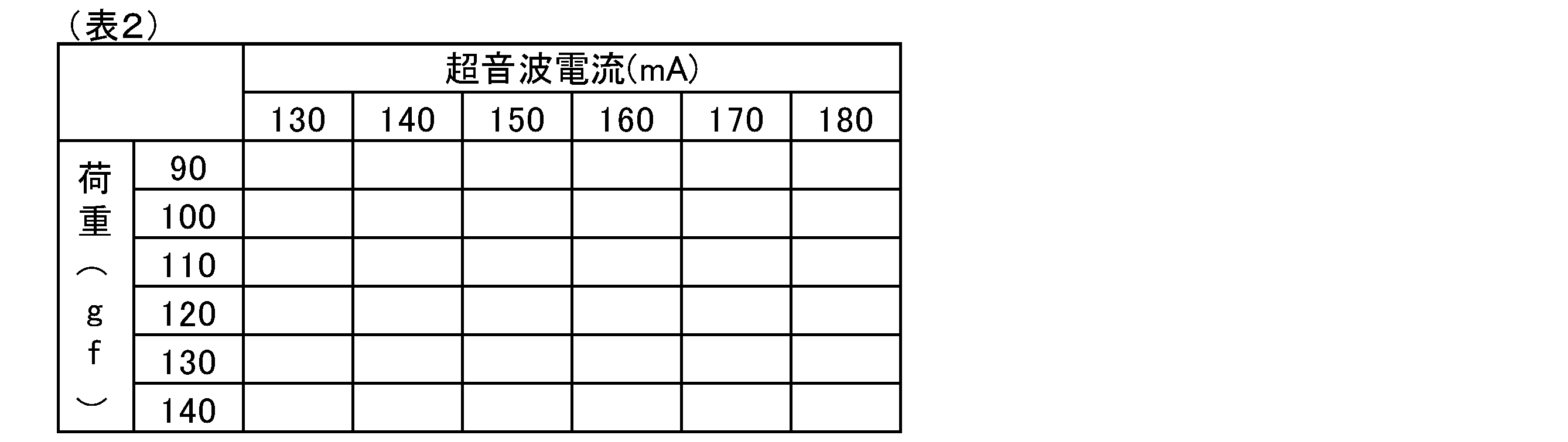
本試験は、実施例及び比較例の各ワイヤについて、(i)ワイヤの製造当日と、ワイヤ製造後に(ii)大気中で1週間保管後、(iii)大気中で2週間保管後、(iv)大気中で3週間保管後、(v)大気中で4週間保管後の、異なる5つの時期に実施した。詳細には、市販のワイヤボンダを用いて、リードフレームのリード部分に、各条件につき200本ずつボンディングを行った。リードフレームには、Agめっきを施したリードフレームを用い、ステージ温度200℃、フォーミングガス(5%H2-N2)0.5l/分流通下にボンディングを行った。そして、不着やボンダの停止の問題なしに連続ボンディングできた条件の数を求め、以下の基準に従って、評価した。
評価基準:
◎:33条件以上
○:30~32条件
△:26~29条件
×:25条件以下
◎:33条件以上
○:30~32条件
△:26~29条件
×:25条件以下
[ループ形状安定性]
ループ形状安定性(ループプロファイルの再現性)は、ワイヤ長が3mm、ループ高さが250μmとなるように台形ループを40本接続し、高さの標準偏差より評価した。高さ測定には光学顕微鏡を使用し、位置はループの最頂点の近傍と、ループの中央部の2箇所で測定した。ループ高さの標準偏差がワイヤ径の1/2以上であれば、バラツキが大きいと判断し、1/2未満であればバラツキは小さく良好であると判断した。そして、表3に示す基準に従って、評価した。
ループ形状安定性(ループプロファイルの再現性)は、ワイヤ長が3mm、ループ高さが250μmとなるように台形ループを40本接続し、高さの標準偏差より評価した。高さ測定には光学顕微鏡を使用し、位置はループの最頂点の近傍と、ループの中央部の2箇所で測定した。ループ高さの標準偏差がワイヤ径の1/2以上であれば、バラツキが大きいと判断し、1/2未満であればバラツキは小さく良好であると判断した。そして、表3に示す基準に従って、評価した。

実施例及び比較例の評価結果を表4に示す。
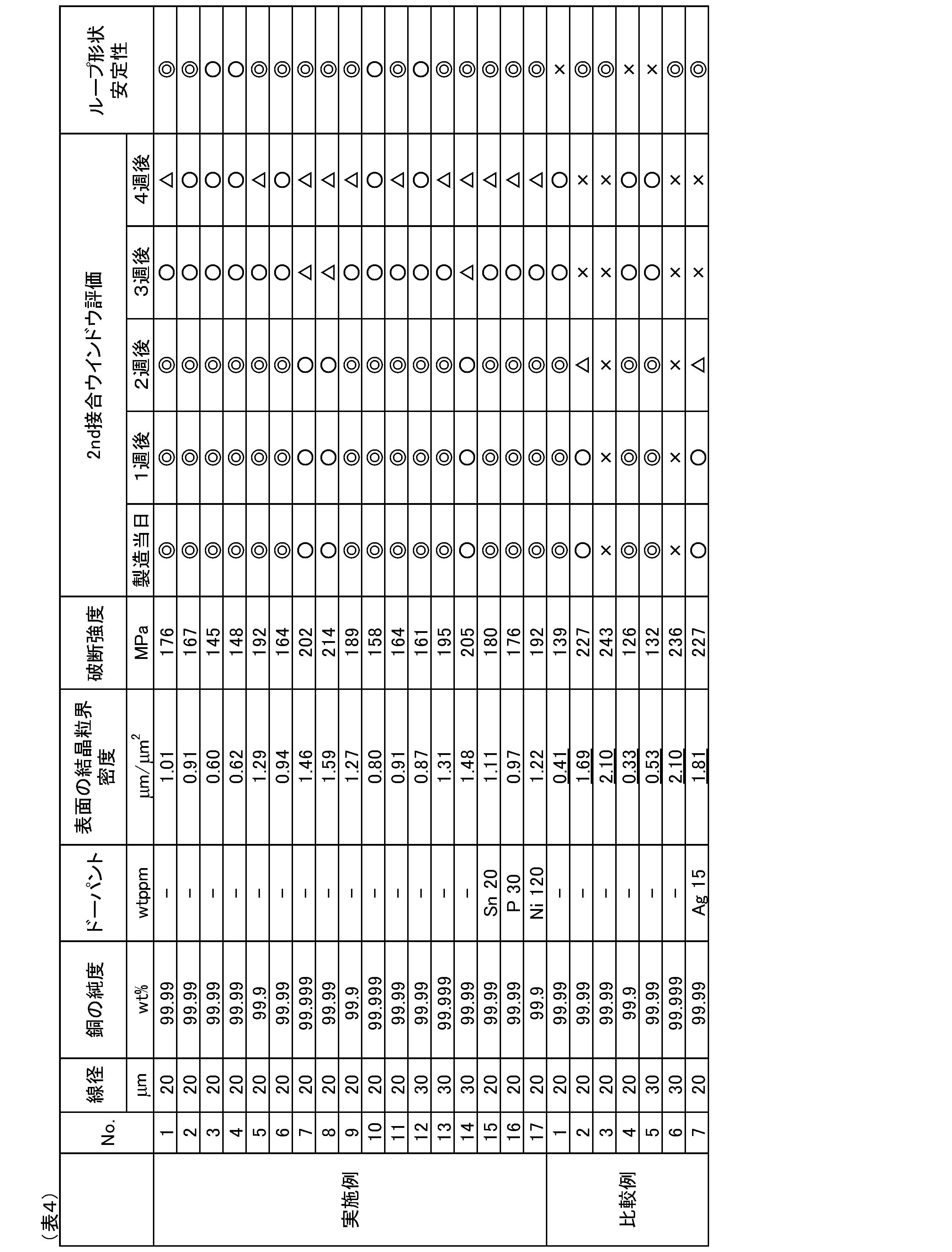
実施例No.1~17はいずれも、ワイヤの表面の結晶粒界密度が本発明範囲内にあり、大気中で保管した後も酸化劣化による接続不良を抑制することができ、広いプロセスウィンドウを確保することができることを確認した。さらに、実施例No.1~17はいずれも、ループプロファイルの再現性に優れ、良好なループ形状安定性を呈することを確認した。なお、ワイヤの表面をSEM観察(倍率10,000倍;二次電子像)したところ、実施例No.1~6、9~13、15~17に関しては表面欠陥は観察されず、また、実施例No.7、8及び14に関しては表面欠陥が若干観察された。なお、表面欠陥とは、光学顕微鏡で見えるようなキズ、削れではなく、電子顕微鏡で観察できる微小な欠陥である。表面欠陥は、主に伸線時にダイスとの接触によって形成されるものと考えられる。
他方、比較例No.1~7は、ワイヤの表面の結晶粒界密度が本発明範囲外であり、酸化劣化による接続不良が生じ、狭いプロセスウィンドウに帰着したり、ループ形状安定性に劣ったりすることを確認した。なお、ワイヤの表面をSEM観察(倍率10,000倍;二次電子像)したところ、比較例No.1、4、5に関しては表面欠陥は観察されず、比較例No.2、7に関しては表面欠陥が若干観察され、比較例No.3、6に関しては表面欠陥が多く観察された。
また、線径100μm、200μmなどのワイヤに関しても、ワイヤの表面の結晶粒界密度が本発明範囲内にあると、上記実施例と同様の挙動を示すことを確認した。
他方、比較例No.1~7は、ワイヤの表面の結晶粒界密度が本発明範囲外であり、酸化劣化による接続不良が生じ、狭いプロセスウィンドウに帰着したり、ループ形状安定性に劣ったりすることを確認した。なお、ワイヤの表面をSEM観察(倍率10,000倍;二次電子像)したところ、比較例No.1、4、5に関しては表面欠陥は観察されず、比較例No.2、7に関しては表面欠陥が若干観察され、比較例No.3、6に関しては表面欠陥が多く観察された。
また、線径100μm、200μmなどのワイヤに関しても、ワイヤの表面の結晶粒界密度が本発明範囲内にあると、上記実施例と同様の挙動を示すことを確認した。
Claims (7)
- 表面の結晶粒界密度が0.6(μm/μm2)以上1.6(μm/μm2)以下である、半導体装置用銅ボンディングワイヤ。
- 表面の結晶粒界密度が、EBSD法により測定点間隔0.06μm以上0.6μm以下で測定し、隣接する測定点間の方位差が15°以上である境界を結晶粒界とみなした場合の結晶粒界の総長さ(μm)を測定面積(μm2)で除して算出される、請求項1に記載の銅ボンディングワイヤ。
- 表面の結晶粒界密度が、ワイヤ長手軸に垂直な方向におけるワイヤの幅の中心が測定面の幅の中心となるように位置決めし、かつ、測定面の幅がワイヤ直径の20%以上40%以下、測定面の長さが測定面の幅の5倍となる条件にて測定される、請求項2に記載の銅ボンディングワイヤ。
- 純度99.9質量%以上の銅からなる、請求項1~3の何れか1項に記載の銅ボンディングワイヤ。
- ワイヤ直径が15μm以上300μm以下である、請求項1~4の何れか1項に記載の銅ボンディングワイヤ。
- 破断強度が145MPa以上である、請求項1~5の何れか1項に記載の銅ボンディングワイヤ。
- 請求項1~6の何れか1項に記載の銅ボンディングワイヤを含む半導体装置。
Priority Applications (5)
| Application Number | Priority Date | Filing Date | Title |
|---|---|---|---|
| KR1020227017877A KR20220106134A (ko) | 2019-12-02 | 2020-11-20 | 반도체 장치용 구리 본딩 와이어 및 반도체 장치 |
| JP2021562572A JPWO2021111908A1 (ja) | 2019-12-02 | 2020-11-20 | |
| EP20896310.8A EP4071256A4 (en) | 2019-12-02 | 2020-11-20 | COPPER CONNECTION WIRE OF SEMICONDUCTOR DEVICE AND SEMICONDUCTOR DEVICE |
| US17/781,316 US20230013769A1 (en) | 2019-12-02 | 2020-11-20 | Copper bonding wire for semiconductor devices and semiconductor device |
| CN202080083559.9A CN114761591B (zh) | 2019-12-02 | 2020-11-20 | 半导体装置用铜接合线及半导体装置 |
Applications Claiming Priority (2)
| Application Number | Priority Date | Filing Date | Title |
|---|---|---|---|
| JP2019218023 | 2019-12-02 | ||
| JP2019-218023 | 2019-12-02 |
Publications (1)
| Publication Number | Publication Date |
|---|---|
| WO2021111908A1 true WO2021111908A1 (ja) | 2021-06-10 |
Family
ID=76222139
Family Applications (1)
| Application Number | Title | Priority Date | Filing Date |
|---|---|---|---|
| PCT/JP2020/043446 WO2021111908A1 (ja) | 2019-12-02 | 2020-11-20 | 半導体装置用銅ボンディングワイヤ及び半導体装置 |
Country Status (7)
| Country | Link |
|---|---|
| US (1) | US20230013769A1 (ja) |
| EP (1) | EP4071256A4 (ja) |
| JP (1) | JPWO2021111908A1 (ja) |
| KR (1) | KR20220106134A (ja) |
| CN (1) | CN114761591B (ja) |
| TW (1) | TW202129020A (ja) |
| WO (1) | WO2021111908A1 (ja) |
Cited By (1)
| Publication number | Priority date | Publication date | Assignee | Title |
|---|---|---|---|---|
| WO2024058211A1 (ja) * | 2022-09-16 | 2024-03-21 | 田中電子工業株式会社 | 銅ボンディングワイヤ、銅ボンディングワイヤの製造方法及び半導体装置 |
Citations (7)
| Publication number | Priority date | Publication date | Assignee | Title |
|---|---|---|---|---|
| JPS6148543A (ja) | 1984-08-10 | 1986-03-10 | Sumitomo Electric Ind Ltd | 半導体素子結線用銅合金線 |
| JP2002246542A (ja) | 2001-02-15 | 2002-08-30 | Matsushita Electric Ind Co Ltd | パワーモジュール及びその製造方法 |
| JP2009140953A (ja) * | 2007-12-03 | 2009-06-25 | Nippon Steel Materials Co Ltd | 半導体装置用ボンディングワイヤ |
| JP2013026475A (ja) * | 2011-07-21 | 2013-02-04 | Hitachi Cable Ltd | 銅ボンディングワイヤ |
| WO2017221770A1 (ja) | 2016-06-20 | 2017-12-28 | 日鉄住金マイクロメタル株式会社 | 半導体装置用銅合金ボンディングワイヤ |
| JP2018503743A (ja) | 2014-12-22 | 2018-02-08 | ヘレウス マテリアルズ シンガポール ピーティーイー. リミテッド | ニッケルを含む耐食性および耐湿性銅系ボンディングワイヤ |
| WO2018212327A1 (ja) * | 2017-05-18 | 2018-11-22 | 新日鐵住金株式会社 | 線材、鋼線、及び鋼線の製造方法 |
Family Cites Families (3)
| Publication number | Priority date | Publication date | Assignee | Title |
|---|---|---|---|---|
| JP3838521B1 (ja) * | 2005-12-27 | 2006-10-25 | 株式会社神戸製鋼所 | 高強度および優れた曲げ加工性を備えた銅合金およびその製造方法 |
| KR101704839B1 (ko) * | 2009-06-24 | 2017-02-08 | 신닛테츠스미킹 마테리알즈 가부시키가이샤 | 반도체용 구리 합금 본딩 와이어 |
| JP5053456B1 (ja) * | 2011-12-28 | 2012-10-17 | 田中電子工業株式会社 | 半導体装置接続用高純度銅細線 |
-
2020
- 2020-11-20 KR KR1020227017877A patent/KR20220106134A/ko unknown
- 2020-11-20 US US17/781,316 patent/US20230013769A1/en active Pending
- 2020-11-20 CN CN202080083559.9A patent/CN114761591B/zh active Active
- 2020-11-20 WO PCT/JP2020/043446 patent/WO2021111908A1/ja active Application Filing
- 2020-11-20 JP JP2021562572A patent/JPWO2021111908A1/ja active Pending
- 2020-11-20 EP EP20896310.8A patent/EP4071256A4/en active Pending
- 2020-11-26 TW TW109141597A patent/TW202129020A/zh unknown
Patent Citations (8)
| Publication number | Priority date | Publication date | Assignee | Title |
|---|---|---|---|---|
| JPS6148543A (ja) | 1984-08-10 | 1986-03-10 | Sumitomo Electric Ind Ltd | 半導体素子結線用銅合金線 |
| JP2002246542A (ja) | 2001-02-15 | 2002-08-30 | Matsushita Electric Ind Co Ltd | パワーモジュール及びその製造方法 |
| JP2009140953A (ja) * | 2007-12-03 | 2009-06-25 | Nippon Steel Materials Co Ltd | 半導体装置用ボンディングワイヤ |
| JP2013026475A (ja) * | 2011-07-21 | 2013-02-04 | Hitachi Cable Ltd | 銅ボンディングワイヤ |
| JP2018503743A (ja) | 2014-12-22 | 2018-02-08 | ヘレウス マテリアルズ シンガポール ピーティーイー. リミテッド | ニッケルを含む耐食性および耐湿性銅系ボンディングワイヤ |
| WO2017221770A1 (ja) | 2016-06-20 | 2017-12-28 | 日鉄住金マイクロメタル株式会社 | 半導体装置用銅合金ボンディングワイヤ |
| JP2019149559A (ja) * | 2016-06-20 | 2019-09-05 | 日鉄マイクロメタル株式会社 | 半導体装置用銅合金ボンディングワイヤ |
| WO2018212327A1 (ja) * | 2017-05-18 | 2018-11-22 | 新日鐵住金株式会社 | 線材、鋼線、及び鋼線の製造方法 |
Non-Patent Citations (1)
| Title |
|---|
| See also references of EP4071256A4 |
Cited By (1)
| Publication number | Priority date | Publication date | Assignee | Title |
|---|---|---|---|---|
| WO2024058211A1 (ja) * | 2022-09-16 | 2024-03-21 | 田中電子工業株式会社 | 銅ボンディングワイヤ、銅ボンディングワイヤの製造方法及び半導体装置 |
Also Published As
| Publication number | Publication date |
|---|---|
| US20230013769A1 (en) | 2023-01-19 |
| TW202129020A (zh) | 2021-08-01 |
| JPWO2021111908A1 (ja) | 2021-06-10 |
| EP4071256A1 (en) | 2022-10-12 |
| CN114761591A (zh) | 2022-07-15 |
| EP4071256A4 (en) | 2023-11-29 |
| CN114761591B (zh) | 2024-01-05 |
| KR20220106134A (ko) | 2022-07-28 |
Similar Documents
| Publication | Publication Date | Title |
|---|---|---|
| KR101659254B1 (ko) | 반도체 장치용 본딩 와이어 | |
| WO2020208839A1 (ja) | 金被覆銀ボンディングワイヤとその製造方法、及び半導体装置とその製造方法 | |
| TW202146672A (zh) | 半導體裝置用接合線 | |
| US11251153B2 (en) | Noble metal-coated silver wire for ball bonding, and semiconductor device using noble metal-coated silver wire for ball bonding | |
| WO2021111908A1 (ja) | 半導体装置用銅ボンディングワイヤ及び半導体装置 | |
| US20230387066A1 (en) | Bonding wire for semiconductor devices | |
| US20230335528A1 (en) | Bonding wire for semiconductor devices | |
| JP2017045924A (ja) | 銅合金ボンディングワイヤ | |
| JP2011192840A (ja) | 半導体素子用平角状アルミニウム被覆銅リボン | |
| US11456271B2 (en) | Noble metal-coated silver wire for ball bonding and method for producing the same, and semiconductor device using noble metal-coated silver wire for ball bonding and method for producing the same | |
| JP4260337B2 (ja) | 半導体実装用のボンディングワイヤ | |
| EP4361300A1 (en) | Semiconductor device bonding wire | |
| JP7494400B1 (ja) | ボンディングワイヤ | |
| EP4361301A1 (en) | Bonding wire for semiconductor device | |
| EP4361298A1 (en) | Bonding wire for semiconductor device | |
| WO2016104121A1 (ja) | 銅ボンディングワイヤ | |
| EP4234734A1 (en) | Ag alloy bonding wire for semiconductor device | |
| US20230154884A1 (en) | Ag ALLOY BONDING WIRE FOR SEMICONDUCTOR DEVICES AND SEMICONDUCTOR DEVICE | |
| CN107109533B (zh) | 用于半导体装置的接合电线 | |
| JP2006073693A (ja) | ボンディングワイヤ |
Legal Events
| Date | Code | Title | Description |
|---|---|---|---|
| 121 | Ep: the epo has been informed by wipo that ep was designated in this application |
Ref document number: 20896310 Country of ref document: EP Kind code of ref document: A1 |
|
| WWE | Wipo information: entry into national phase |
Ref document number: 2021562572 Country of ref document: JP |
|
| NENP | Non-entry into the national phase |
Ref country code: DE |
|
| ENP | Entry into the national phase |
Ref document number: 2020896310 Country of ref document: EP Effective date: 20220704 |