WO2021111843A1 - 回路基板のハンダ付け構造 - Google Patents
回路基板のハンダ付け構造 Download PDFInfo
- Publication number
- WO2021111843A1 WO2021111843A1 PCT/JP2020/042359 JP2020042359W WO2021111843A1 WO 2021111843 A1 WO2021111843 A1 WO 2021111843A1 JP 2020042359 W JP2020042359 W JP 2020042359W WO 2021111843 A1 WO2021111843 A1 WO 2021111843A1
- Authority
- WO
- WIPO (PCT)
- Prior art keywords
- circuit board
- slit hole
- lead plate
- soldering structure
- soldered
- Prior art date
- Legal status (The legal status is an assumption and is not a legal conclusion. Google has not performed a legal analysis and makes no representation as to the accuracy of the status listed.)
- Ceased
Links
Images




Classifications
-
- H—ELECTRICITY
- H01—ELECTRIC ELEMENTS
- H01M—PROCESSES OR MEANS, e.g. BATTERIES, FOR THE DIRECT CONVERSION OF CHEMICAL ENERGY INTO ELECTRICAL ENERGY
- H01M50/00—Constructional details or processes of manufacture of the non-active parts of electrochemical cells other than fuel cells, e.g. hybrid cells
- H01M50/50—Current conducting connections for cells or batteries
- H01M50/502—Interconnectors for connecting terminals of adjacent batteries; Interconnectors for connecting cells outside a battery casing
- H01M50/519—Interconnectors for connecting terminals of adjacent batteries; Interconnectors for connecting cells outside a battery casing comprising printed circuit boards [PCB]
-
- H—ELECTRICITY
- H05—ELECTRIC TECHNIQUES NOT OTHERWISE PROVIDED FOR
- H05K—PRINTED CIRCUITS; CASINGS OR CONSTRUCTIONAL DETAILS OF ELECTRIC APPARATUS; MANUFACTURE OF ASSEMBLAGES OF ELECTRICAL COMPONENTS
- H05K3/00—Apparatus or processes for manufacturing printed circuits
- H05K3/30—Assembling printed circuits with electric components, e.g. with resistors
- H05K3/32—Assembling printed circuits with electric components, e.g. with resistors electrically connecting electric components or wires to printed circuits
- H05K3/34—Assembling printed circuits with electric components, e.g. with resistors electrically connecting electric components or wires to printed circuits by soldering
- H05K3/3405—Edge mounted components, e.g. terminals
-
- H—ELECTRICITY
- H01—ELECTRIC ELEMENTS
- H01M—PROCESSES OR MEANS, e.g. BATTERIES, FOR THE DIRECT CONVERSION OF CHEMICAL ENERGY INTO ELECTRICAL ENERGY
- H01M50/00—Constructional details or processes of manufacture of the non-active parts of electrochemical cells other than fuel cells, e.g. hybrid cells
- H01M50/20—Mountings; Secondary casings or frames; Racks, modules or packs; Suspension devices; Shock absorbers; Transport or carrying devices; Holders
- H01M50/204—Racks, modules or packs for multiple batteries or multiple cells
- H01M50/207—Racks, modules or packs for multiple batteries or multiple cells characterised by their shape
- H01M50/213—Racks, modules or packs for multiple batteries or multiple cells characterised by their shape adapted for cells having curved cross-section, e.g. round or elliptic
-
- H—ELECTRICITY
- H01—ELECTRIC ELEMENTS
- H01M—PROCESSES OR MEANS, e.g. BATTERIES, FOR THE DIRECT CONVERSION OF CHEMICAL ENERGY INTO ELECTRICAL ENERGY
- H01M50/00—Constructional details or processes of manufacture of the non-active parts of electrochemical cells other than fuel cells, e.g. hybrid cells
- H01M50/20—Mountings; Secondary casings or frames; Racks, modules or packs; Suspension devices; Shock absorbers; Transport or carrying devices; Holders
- H01M50/284—Mountings; Secondary casings or frames; Racks, modules or packs; Suspension devices; Shock absorbers; Transport or carrying devices; Holders with incorporated circuit boards, e.g. printed circuit boards [PCB]
- H01M50/287—Fixing of circuit boards to lids or covers
-
- H—ELECTRICITY
- H01—ELECTRIC ELEMENTS
- H01M—PROCESSES OR MEANS, e.g. BATTERIES, FOR THE DIRECT CONVERSION OF CHEMICAL ENERGY INTO ELECTRICAL ENERGY
- H01M50/00—Constructional details or processes of manufacture of the non-active parts of electrochemical cells other than fuel cells, e.g. hybrid cells
- H01M50/20—Mountings; Secondary casings or frames; Racks, modules or packs; Suspension devices; Shock absorbers; Transport or carrying devices; Holders
- H01M50/296—Mountings; Secondary casings or frames; Racks, modules or packs; Suspension devices; Shock absorbers; Transport or carrying devices; Holders characterised by terminals of battery packs
-
- H—ELECTRICITY
- H01—ELECTRIC ELEMENTS
- H01M—PROCESSES OR MEANS, e.g. BATTERIES, FOR THE DIRECT CONVERSION OF CHEMICAL ENERGY INTO ELECTRICAL ENERGY
- H01M50/00—Constructional details or processes of manufacture of the non-active parts of electrochemical cells other than fuel cells, e.g. hybrid cells
- H01M50/50—Current conducting connections for cells or batteries
- H01M50/502—Interconnectors for connecting terminals of adjacent batteries; Interconnectors for connecting cells outside a battery casing
- H01M50/503—Interconnectors for connecting terminals of adjacent batteries; Interconnectors for connecting cells outside a battery casing characterised by the shape of the interconnectors
-
- H—ELECTRICITY
- H01—ELECTRIC ELEMENTS
- H01M—PROCESSES OR MEANS, e.g. BATTERIES, FOR THE DIRECT CONVERSION OF CHEMICAL ENERGY INTO ELECTRICAL ENERGY
- H01M50/00—Constructional details or processes of manufacture of the non-active parts of electrochemical cells other than fuel cells, e.g. hybrid cells
- H01M50/50—Current conducting connections for cells or batteries
- H01M50/502—Interconnectors for connecting terminals of adjacent batteries; Interconnectors for connecting cells outside a battery casing
- H01M50/521—Interconnectors for connecting terminals of adjacent batteries; Interconnectors for connecting cells outside a battery casing characterised by the material
- H01M50/522—Inorganic material
-
- H—ELECTRICITY
- H01—ELECTRIC ELEMENTS
- H01M—PROCESSES OR MEANS, e.g. BATTERIES, FOR THE DIRECT CONVERSION OF CHEMICAL ENERGY INTO ELECTRICAL ENERGY
- H01M50/00—Constructional details or processes of manufacture of the non-active parts of electrochemical cells other than fuel cells, e.g. hybrid cells
- H01M50/50—Current conducting connections for cells or batteries
- H01M50/543—Terminals
- H01M50/552—Terminals characterised by their shape
- H01M50/559—Terminals adapted for cells having curved cross-section, e.g. round, elliptic or button cells
-
- H—ELECTRICITY
- H05—ELECTRIC TECHNIQUES NOT OTHERWISE PROVIDED FOR
- H05K—PRINTED CIRCUITS; CASINGS OR CONSTRUCTIONAL DETAILS OF ELECTRIC APPARATUS; MANUFACTURE OF ASSEMBLAGES OF ELECTRICAL COMPONENTS
- H05K1/00—Printed circuits
- H05K1/02—Details
-
- H—ELECTRICITY
- H01—ELECTRIC ELEMENTS
- H01R—ELECTRICALLY-CONDUCTIVE CONNECTIONS; STRUCTURAL ASSOCIATIONS OF A PLURALITY OF MUTUALLY-INSULATED ELECTRICAL CONNECTING ELEMENTS; COUPLING DEVICES; CURRENT COLLECTORS
- H01R12/00—Structural associations of a plurality of mutually-insulated electrical connecting elements, specially adapted for printed circuits, e.g. printed circuit boards [PCB], flat or ribbon cables, or like generally planar structures, e.g. terminal strips, terminal blocks; Coupling devices specially adapted for printed circuits, flat or ribbon cables, or like generally planar structures; Terminals specially adapted for contact with, or insertion into, printed circuits, flat or ribbon cables, or like generally planar structures
- H01R12/50—Fixed connections
- H01R12/51—Fixed connections for rigid printed circuits or like structures
- H01R12/55—Fixed connections for rigid printed circuits or like structures characterised by the terminals
- H01R12/58—Fixed connections for rigid printed circuits or like structures characterised by the terminals terminals for insertion into holes
-
- H—ELECTRICITY
- H05—ELECTRIC TECHNIQUES NOT OTHERWISE PROVIDED FOR
- H05K—PRINTED CIRCUITS; CASINGS OR CONSTRUCTIONAL DETAILS OF ELECTRIC APPARATUS; MANUFACTURE OF ASSEMBLAGES OF ELECTRICAL COMPONENTS
- H05K2201/00—Indexing scheme relating to printed circuits covered by H05K1/00
- H05K2201/09—Shape and layout
- H05K2201/09009—Substrate related
- H05K2201/09063—Holes or slots in insulating substrate not used for electrical connections
-
- H—ELECTRICITY
- H05—ELECTRIC TECHNIQUES NOT OTHERWISE PROVIDED FOR
- H05K—PRINTED CIRCUITS; CASINGS OR CONSTRUCTIONAL DETAILS OF ELECTRIC APPARATUS; MANUFACTURE OF ASSEMBLAGES OF ELECTRICAL COMPONENTS
- H05K2201/00—Indexing scheme relating to printed circuits covered by H05K1/00
- H05K2201/10—Details of components or other objects attached to or integrated in a printed circuit board
- H05K2201/10007—Types of components
- H05K2201/10037—Printed or non-printed battery
-
- H—ELECTRICITY
- H05—ELECTRIC TECHNIQUES NOT OTHERWISE PROVIDED FOR
- H05K—PRINTED CIRCUITS; CASINGS OR CONSTRUCTIONAL DETAILS OF ELECTRIC APPARATUS; MANUFACTURE OF ASSEMBLAGES OF ELECTRICAL COMPONENTS
- H05K2201/00—Indexing scheme relating to printed circuits covered by H05K1/00
- H05K2201/10—Details of components or other objects attached to or integrated in a printed circuit board
- H05K2201/10227—Other objects, e.g. metallic pieces
- H05K2201/10272—Busbars, i.e. thick metal bars mounted on the printed circuit board [PCB] as high-current conductors
-
- H—ELECTRICITY
- H05—ELECTRIC TECHNIQUES NOT OTHERWISE PROVIDED FOR
- H05K—PRINTED CIRCUITS; CASINGS OR CONSTRUCTIONAL DETAILS OF ELECTRIC APPARATUS; MANUFACTURE OF ASSEMBLAGES OF ELECTRICAL COMPONENTS
- H05K2201/00—Indexing scheme relating to printed circuits covered by H05K1/00
- H05K2201/10—Details of components or other objects attached to or integrated in a printed circuit board
- H05K2201/10227—Other objects, e.g. metallic pieces
- H05K2201/10295—Metallic connector elements partly mounted in a hole of the PCB
-
- H—ELECTRICITY
- H05—ELECTRIC TECHNIQUES NOT OTHERWISE PROVIDED FOR
- H05K—PRINTED CIRCUITS; CASINGS OR CONSTRUCTIONAL DETAILS OF ELECTRIC APPARATUS; MANUFACTURE OF ASSEMBLAGES OF ELECTRICAL COMPONENTS
- H05K2201/00—Indexing scheme relating to printed circuits covered by H05K1/00
- H05K2201/10—Details of components or other objects attached to or integrated in a printed circuit board
- H05K2201/10227—Other objects, e.g. metallic pieces
- H05K2201/1034—Edge terminals, i.e. separate pieces of metal attached to the edge of the printed circuit board [PCB]
-
- H—ELECTRICITY
- H05—ELECTRIC TECHNIQUES NOT OTHERWISE PROVIDED FOR
- H05K—PRINTED CIRCUITS; CASINGS OR CONSTRUCTIONAL DETAILS OF ELECTRIC APPARATUS; MANUFACTURE OF ASSEMBLAGES OF ELECTRICAL COMPONENTS
- H05K2201/00—Indexing scheme relating to printed circuits covered by H05K1/00
- H05K2201/10—Details of components or other objects attached to or integrated in a printed circuit board
- H05K2201/10613—Details of electrical connections of non-printed components, e.g. special leads
- H05K2201/10742—Details of leads
- H05K2201/1075—Shape details
- H05K2201/10757—Bent leads
-
- H—ELECTRICITY
- H05—ELECTRIC TECHNIQUES NOT OTHERWISE PROVIDED FOR
- H05K—PRINTED CIRCUITS; CASINGS OR CONSTRUCTIONAL DETAILS OF ELECTRIC APPARATUS; MANUFACTURE OF ASSEMBLAGES OF ELECTRICAL COMPONENTS
- H05K2201/00—Indexing scheme relating to printed circuits covered by H05K1/00
- H05K2201/10—Details of components or other objects attached to or integrated in a printed circuit board
- H05K2201/10613—Details of electrical connections of non-printed components, e.g. special leads
- H05K2201/10742—Details of leads
- H05K2201/1075—Shape details
- H05K2201/1078—Leads having locally deformed portion, e.g. for retention
-
- H—ELECTRICITY
- H05—ELECTRIC TECHNIQUES NOT OTHERWISE PROVIDED FOR
- H05K—PRINTED CIRCUITS; CASINGS OR CONSTRUCTIONAL DETAILS OF ELECTRIC APPARATUS; MANUFACTURE OF ASSEMBLAGES OF ELECTRICAL COMPONENTS
- H05K2201/00—Indexing scheme relating to printed circuits covered by H05K1/00
- H05K2201/10—Details of components or other objects attached to or integrated in a printed circuit board
- H05K2201/10613—Details of electrical connections of non-printed components, e.g. special leads
- H05K2201/10742—Details of leads
- H05K2201/1075—Shape details
- H05K2201/10787—Leads having protrusions, e.g. for retention or insert stop
-
- H—ELECTRICITY
- H05—ELECTRIC TECHNIQUES NOT OTHERWISE PROVIDED FOR
- H05K—PRINTED CIRCUITS; CASINGS OR CONSTRUCTIONAL DETAILS OF ELECTRIC APPARATUS; MANUFACTURE OF ASSEMBLAGES OF ELECTRICAL COMPONENTS
- H05K2201/00—Indexing scheme relating to printed circuits covered by H05K1/00
- H05K2201/10—Details of components or other objects attached to or integrated in a printed circuit board
- H05K2201/10613—Details of electrical connections of non-printed components, e.g. special leads
- H05K2201/10742—Details of leads
- H05K2201/1075—Shape details
- H05K2201/10818—Flat leads
Definitions
- the present invention relates to a soldering structure of a circuit board, and more particularly to a soldering structure of a circuit board in which a lead plate is inserted into a slit hole provided in the circuit board and soldered to a conductive pattern on the outer peripheral edge of the slit hole. ..
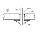
- soldering structure In this soldering structure, as shown in FIG. 1
- a metal plate 102 which is a lead plate, is inserted and immersed in a solder bath in a state where a metal film 105 is formed on the inner surface of a slit hole 103A provided in the circuit board 103. Soldering 106.
- a metal plate can be used as a lead plate, and the lead plate and the circuit board can be soldered.
- heated molten solder flows into the gap formed between the lead plate and the inner surface of the slit hole, and the molten solder is adhered to both the surface of the lead plate and the metal film on the inner surface of the slit hole for soldering. Will be done. It is important that the molten solder that has flowed into the gap is cooled and strongly adheres to the surfaces of both the lead plate and the metal film for electrical connection.
- the molten solder held at this temperature in the solder gap easily flows, and causes various harmful effects to flow down from the solder gap.
- a solder ball that causes thermal damage to a component placed below the circuit board or is dropped and cooled in a granular manner short-circuits the electronic circuit placed below and causes a failure.
- the present invention has been developed for the purpose of eliminating the above-mentioned drawbacks, and one of the purposes of the present invention is to prevent the molten solder from flowing down while reliably and stably connecting the circuit board and the lead plate.
- the purpose is to provide a soldering structure for a circuit board that can be prevented.
- a lead plate inserted into a slit hole of the circuit board is soldered to a conductive pattern provided along the slit hole.
- the lead plate is a metal plate that is thinner than the opening width of the slit hole and can be elastically deformed, and has a bent portion in which the insertion portion inserted into the slit hole approaches from one facing inner surface of the slit hole toward the other facing inner surface.
- the bent portion is arranged in the slit hole, and both sides of the insertion portion are brought close to or in contact with the facing inner surface of the slit hole, and the insertion portion is soldered to the conductive pattern.
- the above soldering structure has the advantage of being able to prevent the harmful effects of molten solder flowing down while reliably and stably connecting the circuit board and lead plate.
- FIG. 5 is an enlarged cross-sectional view showing a connection portion between a circuit board and a lead plate, and is a cross-sectional view taken along the line VI-VI of FIG. It is an enlarged cross-sectional view which shows another example of the bent part of a lead plate.
- FIG. 5 is an enlarged cross-sectional view showing a connection portion between a circuit board and a lead plate, and is a cross-sectional view taken along line IX-IX of FIG. It is a schematic diagram which shows an example of the conventional soldering structure.
- the circuit board soldering structure according to the first embodiment of the present invention is a circuit board in which a lead plate inserted into a slit hole of the circuit board is soldered to a conductive pattern provided along the slit hole.
- the lead plate is a metal plate that is thinner than the opening width of the slit hole and can be elastically deformed. It has a bent portion that approaches toward it, the bent portion is arranged in the slit hole, and both sides of the insertion portion are close to or in contact with the opposite inner surface of the slit hole, and the insertion portion is soldered to the conductive pattern.
- the soldering structure when the lead plate of the metal plate is inserted into the slit hole, the bent portion of the lead plate narrows the gap between the lead plate and the slit hole, so that the soldering structure flows into the gap between the lead plate and the slit hole.
- the molten solder can prevent the harmful effect of flowing down from the slit hole.
- the above soldering structure can solder the lead plate and the conductive pattern while preventing the molten solder from flowing down from the slit hole, so that the molten solder that has flowed into the slit hole is held in a molten state and is conductive with the lead plate. It has the feature that it can be reliably soldered to the pattern.
- the molten solder is not bonded immediately after it comes into contact with the metal surface to be soldered, but heats the contacted metal surface to form an alloy layer at the interface with the metal and solder it.
- the high-temperature molten solder that heats the metal surface to form an alloy layer has good fluidity and easily flows down from the slit holes, but the above soldering method can prevent the highly fluid molten solder from flowing down from the slit holes. Therefore, the molten solder can be maintained at a high temperature and soldered reliably.
- the bent portion is bent into a staircase shape.
- a metal plate that can be elastically deformed is bent into a stepped shape to form a bent portion, so that the bending process is easy and the manufacturing cost can be reduced. Furthermore, both sides of the lead plate insertion portion have a large area. It has the advantage that it can be placed close to the opposite inner surface of the slit hole, and the molten solder can flow in between the slit hole and the insertion portion without leakage, allowing reliable soldering.
- the bent portion of the lead plate is bent into a chevron shape extending in the longitudinal direction of the inner surface of the slit hole.
- the above soldering structure has the feature that while inserting the insertion part into the slit hole in a vertical position, the chevron bent part can be brought close to the facing inner surface in the long region of the slit hole and soldered reliably.
- the width of the bent portion bent into a chevron shape is made smaller than the thickness of the circuit board.
- the solder flows into the gap in a state where the lead plate elastically presses the inner surface of the slit hole on both sides by the bent portion.
- both sides of the insertion portion are elastically pressed against the facing surfaces of the slit holes by the bending portion, the gaps between the slit holes are surely closed by the bending portion, and the molten solder is more surely flowed down. It has the advantage that the lead plate can be smoothly inserted into the slit hole while being blocked and securely soldered.
- the soldering structure of the circuit board according to the sixth embodiment of the present invention has a plurality of slit holes in which the circuit boards are linearly arranged with each other, and a lead plate is inserted into each of the slit holes. It has a plurality of insertion portions, and each insertion portion is inserted into a slit hole and soldered to a conductive pattern of a circuit board.
- the lead plate is inserted into each of the plurality of slit holes and soldered, so that the lead plate and the circuit board can be soldered more reliably.
- the lead plate since a plurality of slit holes are arranged in a straight line, the lead plate has a feature that one metal plate can be branched to provide a plurality of insertion portions and each insertion portion can be soldered to the slit holes. is there.
- the circuit board soldering structure according to the seventh embodiment of the present invention has a circuit board mounting portion in which the lead plate projects in the width direction along the lower surface of the circuit board, and the circuit board is mounted. It is set on the portion, the bent portion is arranged in the slit hole, and the mounting portion is arranged at a position where the end opening of the slit hole is closed from below.
- the relative position between the circuit board and the lead plate can be specified, and the bent portion provided on the insertion portion can be arranged in the slit hole. ..
- the bent portion is arranged at the exact position of the slit hole to prevent the molten solder from flowing down from the slit hole.
- the circuit board is set on the mounting portion provided on the lead plate to prevent the relative misalignment between the circuit board and the lead plate, and the bent portion is surely formed into a slit hole. Can be placed in the correct position. Therefore, the above soldering structure can surely prevent the molten solder from flowing down from the slit hole. Further, in the above soldering structure, when the circuit board is set on the mounting portion, the mounting portion is at a position of closing the opening formed at the end in the longitudinal direction of the slit hole from below, and the end of the slit hole. It is possible to prevent the molten solder from flowing down from the part.
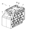
- the battery pack 100 shown in the schematic cross-sectional view of FIG. 1, the perspective view of FIG. 2, and the exploded perspective view of FIG. 3 includes a plurality of rechargeable batteries 1 arranged in parallel posture, and electrode terminals 1a of each battery 1.
- the battery unit 10 is assembled by the lead plate 2 melted and joined to 1b and the circuit board 3 to which the lead plate 2 is soldered, and the battery unit 10 is housed in the outer case 9.
- a plurality of cylindrical batteries 1 are arranged in a fixed position on the battery holder 4 in a posture parallel to each other, and electrode terminals of the respective batteries 1 are arranged on both end surfaces of the battery holder 4. 1a and 1b are exposed, and the lead plate 2 is joined and connected to these electrode terminals 1a and 1b.
- the battery pack 100 in the above figure has an integral structure of a bus bar that cuts one metal plate and connects the batteries 1 in series or in parallel, and a lead plate 2 that connects the bus bar to the circuit board 3.
- a bus bar that cuts one metal plate and connects the batteries 1 in series or in parallel
- a lead plate 2 that connects the bus bar to the circuit board 3.
- the lead plate 2 can be used in a path through which a large current flows, for example, a path through which the charge / discharge current of the battery 1 flows, to reduce power loss.
- the lead plate does not necessarily have to be integrated with the bus bar, and the lead plate and the bus bar may be separate metal plates.
- the lead plate 2 connected to the circuit board 3 can be used, for example, in a signal transmission path or the like, without being used in a path through which a large current flows like the charge / discharge current of the battery 1.
- the lead plate 2 used for the signal transmission path is connected to the circuit board 3 with the following soldering structure, there is a feature that the stability of signal transmission between the lead plate 2 and the circuit board can be improved.
- a slit hole 30 is provided in the circuit board 3, the lead plate 2 is inserted into the slit hole 30, and the lead plate 3 is led to the conductive pattern 31 provided in the circuit board 3.
- the board 2 is soldered and connected.
- the circuit board 3 is connected to the circuit board 3 by providing a conductive pattern 31 along the slit hole 30 and soldering a lead plate 2 to the conductive pattern 31.
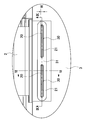
- the plan view of FIG. 4 shows a circuit board 3 provided with a slit hole 30 and a conductive pattern 31.
- the circuit board 3 shown in this figure is provided with a plurality of slit holes 30 arranged in a straight line, and a conductive pattern 31 is provided on the surface of the circuit board 3 along the outer circumference of the slit holes 30.
- the conductive pattern 31 is provided on the surface of the circuit board 3 with a predetermined width along the entire circumference of the slit hole 30.
- the conductive pattern 31 can be provided on both the front and back surfaces of the circuit board 3 along the outer circumference of the slit hole 30.
- the circuit board 3 can preferably have a through-hole structure by providing a conductive pattern on the inner surface of the slit hole 30 continuously with the conductive pattern 31 on the surface.
- the conductive pattern 31 of the through hole has a feature that the lead plate 2 can be soldered more reliably.
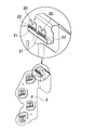
- the lead plate 2 is a metal plate that is thinner than the opening width (W) of the slit hole 30 and can be elastically deformed, and an insertion portion 20 to be inserted into the slit hole 30 is provided at the tip portion.
- the lead plate 2 that is inserted into and soldered to the plurality of slit holes 30 provided in the circuit board 3 is provided with a plurality of branched insertion portions 20 at the tip portion. Since the circuit board 3 shown in FIG. 3 is provided with two rows of slit holes 30 arranged in a straight line, the lead plate 2 is provided with an insertion portion 20 branched into two at the tip portion as shown in FIG. ing.
- the lead plate 2 thinner than the opening width (W) of the slit hole 30 has a gap between it and the facing inner surface 32 of the slit hole 30 in a state of being inserted into the slit hole 30.
- the insertion portion 20 is provided with a bending portion 21 that approaches the slit hole 30 from one facing inner surface 32 toward the other facing inner surface 32. There is.
- the insertion portion 20 having the bent portion 21 is inserted into the slit hole 30 and has both sides close to or in contact with the facing inner surface 32 of the slit hole 30 to reduce the gap with the facing inner surface 32.
- the bent portion 21 is preferably inserted into the slit hole 30, and both sides of the inserted portion 20 are bent into a shape that elastically presses the facing inner surface 32 of the slit hole 30.
- both sides of the insertion portion 20 elastically press the facing surfaces of the slit holes 30 to bring them into contact with each other, so that the gaps in the slit holes 30 are reliably closed and the molten solder is more reliably prevented from flowing down. Can be stopped.
- the bent portion 21 does not necessarily have a shape in which both sides of the insertion portion 20 are elastically pressed against the facing inner surface 32 of the slit hole 30, and the surface of the inserting portion 20 approaches the facing inner surface 32 of the slit hole 30.
- the insertion portion 20 in which the gap between the bent portion 21 and the slit hole 30 is narrowed is inserted into the slit hole 30 of the circuit board 3 and is reliably soldered to the conductive pattern 31 without dropping molten solder from the slit hole 30. ..
- the insertion portion 20 shown in the enlarged cross-sectional view of FIG. 6 is provided with a bent portion 21 by bending a metal plate into a chevron shape extending in the longitudinal direction of the inner surface of the elongated slit hole 30.
- the width (d) of the bent portion 21 bent into a chevron shape is smaller than the thickness (t) of the circuit board 3, and both sides of the chevron portion are bent so as to approach or come into contact with the same facing inner surface 32. ..
- the insertion portion 20 in this figure is the mountain portion of the bent portion 21 and both sides thereof. Contact to reduce the gap or close the gap.
- the insertion portion 20 shown in the cross-sectional view of FIG. 7 is formed by bending a metal plate into a staircase shape to form a bent portion 21.
- the insertion portions 20 in this figure are above and below the bent portion 21, and in the figure, they approach or come into contact with the facing inner surface 32 on the left side above the bent portion 21 and the facing inner surface 32 on the right side below the bent portion 21. Reduce the gap or close the gap.
- the enlarged cross-sectional view of FIG. 8 shows a state in which the lead plate 2 is inserted into the slit hole 30 and the insertion portion 20 of the lead plate 2 is soldered to the conductive pattern 31 of the circuit board 3.
- the lead plate 2 shown in this figure is soldered to the circuit board 3 with molten solder 35 in a state where the bent portion 21 provided in the insertion portion 20 is arranged in the slit hole 30.
- the insertion portion 20 shown in FIG. 8 has the right surface approaching or contacting the facing inner surface 32 of the slit hole 30 and the left surface the surface of the mountain portion of the bending portion 21 approaching or contacting the facing inner surface 32 of the slit hole 30. There is.
- the molten solder 35 heated along the boundary portion between the lead plate 2 and the slit hole 30 is supplied.
- the supplied molten solder 35 heats the conductive pattern 31 of the lead plate 2 and the circuit board 3 and flows along the surfaces of the lead plate 2 and the conductive pattern 31, and melt solder with the surfaces of the lead plate 2 and the conductive pattern 31.
- An alloy layer is formed at the interface with 35 and is surely soldered to the lead plate 2 and the conductive pattern 31.
- the molten solder 35 supplied to the boundary between the lead plate 2 and the slit hole 30 has a bent portion 21 that closes the gap through which the molten solder 35 flows down, and flows down from the slit hole 30 even in a fluid state.
- the lead plate 2 and the conductive pattern 31 are securely soldered without any problem.
- the structure that can prevent the fluid molten solder 35 from flowing down is that the molten solder 35 can heat the lead plate 2 and the conductive pattern 31 until an alloy layer is formed, so that the lead plate 2 and the conductive pattern 31 are surely soldered. it can.
- the lead plate 2 shown in FIGS. 5 and 9 is provided with a mounting portion 22 for setting the circuit board 3 at an accurate position.
- the mounting portion 22 is provided so as to project in the width direction at a position along the lower surface of the circuit board 3 in a state where the circuit board 3 is set.
- the mounting portion 22 is arranged at a fixed position by mounting the lower surface of the circuit board 3 on the mounting portion 22. Since the mounting portion 22 protrudes from the lead plate 2 in the width direction, the mounting portion 22 is arranged at a position where the end portion of the slit hole 30 is closed from below while the circuit board 3 is arranged on the mounting portion 22.
- the circuit board 3 is placed on the mounting portion 22 and set, so that the bending portion 21 is accurately arranged in the slit hole 30, and the insertion portion 20 is inserted into the slit hole 30.
- the gap formed at the end of the hole 30 is closed by the mounting portion 22 from below.
- the bending portion 21 closes the gap formed on both sides of the slit hole 30, and the mounting portion 22 closes the gap formed at the end of the slit hole 30, so that the molten solder 35 is formed from the slit hole 30. It has the feature of being able to reliably prevent it from flowing down.
- the battery pack according to the present invention can be suitably used as a rechargeable battery pack for battery-powered devices such as assisted bicycles, electric bikes, electric wheelchairs, electric carts, cleaners, and electric tools.
Landscapes
- Chemical & Material Sciences (AREA)
- Chemical Kinetics & Catalysis (AREA)
- Electrochemistry (AREA)
- General Chemical & Material Sciences (AREA)
- Engineering & Computer Science (AREA)
- Microelectronics & Electronic Packaging (AREA)
- Inorganic Chemistry (AREA)
- Manufacturing & Machinery (AREA)
- Electric Connection Of Electric Components To Printed Circuits (AREA)
- Coupling Device And Connection With Printed Circuit (AREA)
Priority Applications (4)
| Application Number | Priority Date | Filing Date | Title |
|---|---|---|---|
| JP2021562542A JP7592625B2 (ja) | 2019-12-03 | 2020-11-13 | 回路基板のハンダ付け構造 |
| CN202080076504.5A CN114651533A (zh) | 2019-12-03 | 2020-11-13 | 电路基板的焊接构造 |
| US17/780,800 US11996586B2 (en) | 2019-12-03 | 2020-11-13 | Circuit board soldering structure |
| EP20896476.7A EP4072250B1 (en) | 2019-12-03 | 2020-11-13 | Circuit board soldering structure |
Applications Claiming Priority (2)
| Application Number | Priority Date | Filing Date | Title |
|---|---|---|---|
| JP2019218562 | 2019-12-03 | ||
| JP2019-218562 | 2019-12-03 |
Publications (1)
| Publication Number | Publication Date |
|---|---|
| WO2021111843A1 true WO2021111843A1 (ja) | 2021-06-10 |
Family
ID=76221787
Family Applications (1)
| Application Number | Title | Priority Date | Filing Date |
|---|---|---|---|
| PCT/JP2020/042359 Ceased WO2021111843A1 (ja) | 2019-12-03 | 2020-11-13 | 回路基板のハンダ付け構造 |
Country Status (5)
| Country | Link |
|---|---|
| US (1) | US11996586B2 (https=) |
| EP (1) | EP4072250B1 (https=) |
| JP (1) | JP7592625B2 (https=) |
| CN (1) | CN114651533A (https=) |
| WO (1) | WO2021111843A1 (https=) |
Cited By (1)
| Publication number | Priority date | Publication date | Assignee | Title |
|---|---|---|---|---|
| EP4597731A4 (en) * | 2022-09-26 | 2026-01-21 | Panasonic Energy Co Ltd | ELECTRICAL DEVICE AND ITS MANUFACTURING PROCESS |
Families Citing this family (1)
| Publication number | Priority date | Publication date | Assignee | Title |
|---|---|---|---|---|
| KR20250122876A (ko) * | 2024-02-07 | 2025-08-14 | 삼성에스디아이 주식회사 | 이차전지 팩 |
Citations (7)
| Publication number | Priority date | Publication date | Assignee | Title |
|---|---|---|---|---|
| JPS55137582U (https=) * | 1979-03-20 | 1980-09-30 | ||
| JPS63187348U (https=) * | 1987-05-25 | 1988-11-30 | ||
| JPH0197562U (https=) * | 1987-12-22 | 1989-06-29 | ||
| JPH0428285A (ja) * | 1990-05-23 | 1992-01-30 | Hitachi Chem Co Ltd | 端子付きフレキシブル配線板 |
| JPH0645743A (ja) | 1992-07-24 | 1994-02-18 | Matsushita Electric Ind Co Ltd | 回路基板とそのハンダ付方法 |
| JP2010277796A (ja) * | 2009-05-27 | 2010-12-09 | Sanyo Electric Co Ltd | パック電池 |
| JP2011187915A (ja) * | 2009-09-28 | 2011-09-22 | Kyocera Corp | フレキシブル配線基板とリード端子付き電子部品との接続構造 |
Family Cites Families (8)
| Publication number | Priority date | Publication date | Assignee | Title |
|---|---|---|---|---|
| JPH01207961A (ja) * | 1988-02-15 | 1989-08-21 | Nec Corp | 半導体装置 |
| US5618187A (en) | 1994-11-17 | 1997-04-08 | The Whitaker Corporation | Board mount bus bar contact |
| US7085146B2 (en) | 1999-12-20 | 2006-08-01 | Synqor, Inc. | Flanged terminal pins for DC/DC converters |
| JP2006100408A (ja) | 2004-09-28 | 2006-04-13 | Fujitsu Ten Ltd | 挿入部品およびそのはんだ付け構造 |
| KR100965683B1 (ko) * | 2008-03-31 | 2010-06-24 | 삼성에스디아이 주식회사 | 배터리 팩 |
| US9451710B2 (en) * | 2010-08-26 | 2016-09-20 | Samsung Sdi Co., Ltd. | Battery pack |
| JP6255936B2 (ja) | 2013-11-21 | 2018-01-10 | 三菱電機株式会社 | 半導体装置、半導体装置の製造方法 |
| CN112020783B (zh) | 2018-04-25 | 2023-01-03 | 三洋电机株式会社 | 电池组 |
-
2020
- 2020-11-13 JP JP2021562542A patent/JP7592625B2/ja active Active
- 2020-11-13 EP EP20896476.7A patent/EP4072250B1/en active Active
- 2020-11-13 CN CN202080076504.5A patent/CN114651533A/zh active Pending
- 2020-11-13 WO PCT/JP2020/042359 patent/WO2021111843A1/ja not_active Ceased
- 2020-11-13 US US17/780,800 patent/US11996586B2/en active Active
Patent Citations (7)
| Publication number | Priority date | Publication date | Assignee | Title |
|---|---|---|---|---|
| JPS55137582U (https=) * | 1979-03-20 | 1980-09-30 | ||
| JPS63187348U (https=) * | 1987-05-25 | 1988-11-30 | ||
| JPH0197562U (https=) * | 1987-12-22 | 1989-06-29 | ||
| JPH0428285A (ja) * | 1990-05-23 | 1992-01-30 | Hitachi Chem Co Ltd | 端子付きフレキシブル配線板 |
| JPH0645743A (ja) | 1992-07-24 | 1994-02-18 | Matsushita Electric Ind Co Ltd | 回路基板とそのハンダ付方法 |
| JP2010277796A (ja) * | 2009-05-27 | 2010-12-09 | Sanyo Electric Co Ltd | パック電池 |
| JP2011187915A (ja) * | 2009-09-28 | 2011-09-22 | Kyocera Corp | フレキシブル配線基板とリード端子付き電子部品との接続構造 |
Cited By (1)
| Publication number | Priority date | Publication date | Assignee | Title |
|---|---|---|---|---|
| EP4597731A4 (en) * | 2022-09-26 | 2026-01-21 | Panasonic Energy Co Ltd | ELECTRICAL DEVICE AND ITS MANUFACTURING PROCESS |
Also Published As
| Publication number | Publication date |
|---|---|
| US11996586B2 (en) | 2024-05-28 |
| EP4072250B1 (en) | 2026-01-07 |
| JPWO2021111843A1 (https=) | 2021-06-10 |
| EP4072250A1 (en) | 2022-10-12 |
| CN114651533A (zh) | 2022-06-21 |
| EP4072250A4 (en) | 2023-06-07 |
| JP7592625B2 (ja) | 2024-12-02 |
| US20220416370A1 (en) | 2022-12-29 |
Similar Documents
| Publication | Publication Date | Title |
|---|---|---|
| KR102480781B1 (ko) | 배터리 구조물, 상호연결부, 감지 및 밸런싱을 위한 시스템 및 방법 | |
| CN105745772B (zh) | 电源装置 | |
| JP5068544B2 (ja) | 保護回路基板を含む一体化タイプのキャップ組立品及びこれを含む二次電池 | |
| CN107004821A (zh) | 用于电化学装置的电池接触系统 | |
| CN101552330A (zh) | 电池组 | |
| KR101142622B1 (ko) | 배터리 팩 | |
| JP2002124305A (ja) | 電池パック | |
| WO2021111843A1 (ja) | 回路基板のハンダ付け構造 | |
| CN104577019A (zh) | 电池包 | |
| CN111433942A (zh) | 电池模块 | |
| US20230282945A1 (en) | Battery wiring module | |
| US7781096B2 (en) | Battery case | |
| JP7327664B2 (ja) | 電池パックおよび電子機器 | |
| TW200933683A (en) | Temperature fuse with resistor and battery protection circuit board | |
| KR102829929B1 (ko) | 보호 소자 | |
| US20250364697A1 (en) | Wiring module | |
| US20230076491A1 (en) | Battery pack and electronic device | |
| JPH047568Y2 (https=) | ||
| JP2005285680A (ja) | 電池パック及び電池パックの組立方法 | |
| CN116759761A (zh) | 一种电池和电子设备 | |
| JP3939018B2 (ja) | パック電池 | |
| KR101197036B1 (ko) | 온도휴즈 | |
| KR20250035872A (ko) | 배터리 장치용 회로 어셈블리 및 이를 포함하는 배터리 장치 | |
| KR100753718B1 (ko) | 금속탭 가이드가 구비된 ptc 소자 및 그 제조방법 | |
| JP2009259920A (ja) | 回路基板および回路基板の製造方法 |
Legal Events
| Date | Code | Title | Description |
|---|---|---|---|
| 121 | Ep: the epo has been informed by wipo that ep was designated in this application |
Ref document number: 20896476 Country of ref document: EP Kind code of ref document: A1 |
|
| ENP | Entry into the national phase |
Ref document number: 2021562542 Country of ref document: JP Kind code of ref document: A |
|
| NENP | Non-entry into the national phase |
Ref country code: DE |
|
| ENP | Entry into the national phase |
Ref document number: 2020896476 Country of ref document: EP Effective date: 20220704 |
|
| WWG | Wipo information: grant in national office |
Ref document number: 2020896476 Country of ref document: EP |