WO2021106875A1 - 導光素子および画像表示装置 - Google Patents
導光素子および画像表示装置 Download PDFInfo
- Publication number
- WO2021106875A1 WO2021106875A1 PCT/JP2020/043676 JP2020043676W WO2021106875A1 WO 2021106875 A1 WO2021106875 A1 WO 2021106875A1 JP 2020043676 W JP2020043676 W JP 2020043676W WO 2021106875 A1 WO2021106875 A1 WO 2021106875A1
- Authority
- WO
- WIPO (PCT)
- Prior art keywords
- liquid crystal
- diffraction element
- light guide
- crystal layer
- light
- Prior art date
- Legal status (The legal status is an assumption and is not a legal conclusion. Google has not performed a legal analysis and makes no representation as to the accuracy of the status listed.)
- Ceased
Links
Images




Classifications
-
- G—PHYSICS
- G02—OPTICS
- G02B—OPTICAL ELEMENTS, SYSTEMS OR APPARATUS
- G02B27/00—Optical systems or apparatus not provided for by any of the groups G02B1/00 - G02B26/00, G02B30/00
- G02B27/01—Head-up displays
- G02B27/017—Head mounted
- G02B27/0172—Head mounted characterised by optical features
-
- G—PHYSICS
- G02—OPTICS
- G02F—OPTICAL DEVICES OR ARRANGEMENTS FOR THE CONTROL OF LIGHT BY MODIFICATION OF THE OPTICAL PROPERTIES OF THE MEDIA OF THE ELEMENTS INVOLVED THEREIN; NON-LINEAR OPTICS; FREQUENCY-CHANGING OF LIGHT; OPTICAL LOGIC ELEMENTS; OPTICAL ANALOGUE/DIGITAL CONVERTERS
- G02F1/00—Devices or arrangements for the control of the intensity, colour, phase, polarisation or direction of light arriving from an independent light source, e.g. switching, gating or modulating; Non-linear optics
- G02F1/01—Devices or arrangements for the control of the intensity, colour, phase, polarisation or direction of light arriving from an independent light source, e.g. switching, gating or modulating; Non-linear optics for the control of the intensity, phase, polarisation or colour
- G02F1/13—Devices or arrangements for the control of the intensity, colour, phase, polarisation or direction of light arriving from an independent light source, e.g. switching, gating or modulating; Non-linear optics for the control of the intensity, phase, polarisation or colour based on liquid crystals, e.g. single liquid crystal display cells
- G02F1/133—Constructional arrangements; Operation of liquid crystal cells; Circuit arrangements
- G02F1/1333—Constructional arrangements; Manufacturing methods
- G02F1/1335—Structural association of cells with optical devices, e.g. polarisers or reflectors
- G02F1/133504—Diffusing, scattering, diffracting elements
-
- G—PHYSICS
- G02—OPTICS
- G02B—OPTICAL ELEMENTS, SYSTEMS OR APPARATUS
- G02B5/00—Optical elements other than lenses
- G02B5/18—Diffraction gratings
-
- G—PHYSICS
- G02—OPTICS
- G02B—OPTICAL ELEMENTS, SYSTEMS OR APPARATUS
- G02B5/00—Optical elements other than lenses
- G02B5/18—Diffraction gratings
- G02B5/1814—Diffraction gratings structurally combined with one or more further optical elements, e.g. lenses, mirrors, prisms or other diffraction gratings
- G02B5/1819—Plural gratings positioned on the same surface, e.g. array of gratings
-
- G—PHYSICS
- G02—OPTICS
- G02F—OPTICAL DEVICES OR ARRANGEMENTS FOR THE CONTROL OF LIGHT BY MODIFICATION OF THE OPTICAL PROPERTIES OF THE MEDIA OF THE ELEMENTS INVOLVED THEREIN; NON-LINEAR OPTICS; FREQUENCY-CHANGING OF LIGHT; OPTICAL LOGIC ELEMENTS; OPTICAL ANALOGUE/DIGITAL CONVERTERS
- G02F1/00—Devices or arrangements for the control of the intensity, colour, phase, polarisation or direction of light arriving from an independent light source, e.g. switching, gating or modulating; Non-linear optics
- G02F1/01—Devices or arrangements for the control of the intensity, colour, phase, polarisation or direction of light arriving from an independent light source, e.g. switching, gating or modulating; Non-linear optics for the control of the intensity, phase, polarisation or colour
- G02F1/13—Devices or arrangements for the control of the intensity, colour, phase, polarisation or direction of light arriving from an independent light source, e.g. switching, gating or modulating; Non-linear optics for the control of the intensity, phase, polarisation or colour based on liquid crystals, e.g. single liquid crystal display cells
- G02F1/133—Constructional arrangements; Operation of liquid crystal cells; Circuit arrangements
- G02F1/1333—Constructional arrangements; Manufacturing methods
- G02F1/1335—Structural association of cells with optical devices, e.g. polarisers or reflectors
- G02F1/133524—Light-guides, e.g. fibre-optic bundles, louvered or jalousie light-guides
-
- G—PHYSICS
- G02—OPTICS
- G02F—OPTICAL DEVICES OR ARRANGEMENTS FOR THE CONTROL OF LIGHT BY MODIFICATION OF THE OPTICAL PROPERTIES OF THE MEDIA OF THE ELEMENTS INVOLVED THEREIN; NON-LINEAR OPTICS; FREQUENCY-CHANGING OF LIGHT; OPTICAL LOGIC ELEMENTS; OPTICAL ANALOGUE/DIGITAL CONVERTERS
- G02F1/00—Devices or arrangements for the control of the intensity, colour, phase, polarisation or direction of light arriving from an independent light source, e.g. switching, gating or modulating; Non-linear optics
- G02F1/01—Devices or arrangements for the control of the intensity, colour, phase, polarisation or direction of light arriving from an independent light source, e.g. switching, gating or modulating; Non-linear optics for the control of the intensity, phase, polarisation or colour
- G02F1/13—Devices or arrangements for the control of the intensity, colour, phase, polarisation or direction of light arriving from an independent light source, e.g. switching, gating or modulating; Non-linear optics for the control of the intensity, phase, polarisation or colour based on liquid crystals, e.g. single liquid crystal display cells
- G02F1/133—Constructional arrangements; Operation of liquid crystal cells; Circuit arrangements
- G02F1/1333—Constructional arrangements; Manufacturing methods
- G02F1/1337—Surface-induced orientation of the liquid crystal molecules, e.g. by alignment layers
-
- G—PHYSICS
- G02—OPTICS
- G02F—OPTICAL DEVICES OR ARRANGEMENTS FOR THE CONTROL OF LIGHT BY MODIFICATION OF THE OPTICAL PROPERTIES OF THE MEDIA OF THE ELEMENTS INVOLVED THEREIN; NON-LINEAR OPTICS; FREQUENCY-CHANGING OF LIGHT; OPTICAL LOGIC ELEMENTS; OPTICAL ANALOGUE/DIGITAL CONVERTERS
- G02F1/00—Devices or arrangements for the control of the intensity, colour, phase, polarisation or direction of light arriving from an independent light source, e.g. switching, gating or modulating; Non-linear optics
- G02F1/01—Devices or arrangements for the control of the intensity, colour, phase, polarisation or direction of light arriving from an independent light source, e.g. switching, gating or modulating; Non-linear optics for the control of the intensity, phase, polarisation or colour
- G02F1/13—Devices or arrangements for the control of the intensity, colour, phase, polarisation or direction of light arriving from an independent light source, e.g. switching, gating or modulating; Non-linear optics for the control of the intensity, phase, polarisation or colour based on liquid crystals, e.g. single liquid crystal display cells
- G02F1/137—Devices or arrangements for the control of the intensity, colour, phase, polarisation or direction of light arriving from an independent light source, e.g. switching, gating or modulating; Non-linear optics for the control of the intensity, phase, polarisation or colour based on liquid crystals, e.g. single liquid crystal display cells characterised by the electro-optical or magneto-optical effect, e.g. field-induced phase transition, orientation effect, guest-host interaction or dynamic scattering
- G02F1/13718—Devices or arrangements for the control of the intensity, colour, phase, polarisation or direction of light arriving from an independent light source, e.g. switching, gating or modulating; Non-linear optics for the control of the intensity, phase, polarisation or colour based on liquid crystals, e.g. single liquid crystal display cells characterised by the electro-optical or magneto-optical effect, e.g. field-induced phase transition, orientation effect, guest-host interaction or dynamic scattering based on a change of the texture state of a cholesteric liquid crystal
-
- G—PHYSICS
- G02—OPTICS
- G02B—OPTICAL ELEMENTS, SYSTEMS OR APPARATUS
- G02B27/00—Optical systems or apparatus not provided for by any of the groups G02B1/00 - G02B26/00, G02B30/00
- G02B27/01—Head-up displays
- G02B27/0101—Head-up displays characterised by optical features
- G02B2027/0123—Head-up displays characterised by optical features comprising devices increasing the field of view
-
- G—PHYSICS
- G02—OPTICS
- G02B—OPTICAL ELEMENTS, SYSTEMS OR APPARATUS
- G02B27/00—Optical systems or apparatus not provided for by any of the groups G02B1/00 - G02B26/00, G02B30/00
- G02B27/01—Head-up displays
- G02B27/017—Head mounted
- G02B27/0172—Head mounted characterised by optical features
- G02B2027/0174—Head mounted characterised by optical features holographic
-
- G—PHYSICS
- G02—OPTICS
- G02B—OPTICAL ELEMENTS, SYSTEMS OR APPARATUS
- G02B27/00—Optical systems or apparatus not provided for by any of the groups G02B1/00 - G02B26/00, G02B30/00
- G02B27/01—Head-up displays
- G02B27/017—Head mounted
- G02B2027/0178—Eyeglass type
Definitions
- the present invention relates to a light guide element that propagates light and an image display device that uses this light guide element.
- AR glasses In recent years, AR (Augmented Reality) glasses have been put into practical use, which superimpose virtual images and various information on the scene actually viewed as described in Non-Patent Document 1. There is. AR glasses are also called smart glasses, head-mounted displays (HMD (Head Mounted Display)), AR glasses, and the like.
- HMD Head Mounted Display
- Non-Patent Document 1 As shown in Non-Patent Document 1, as an example, in the AR glass, the image displayed by the display (optical engine) is incident on one end of the light guide plate and propagated, and then emitted from the other end, so that the user can use the AR glass. A virtual image is superimposed on the actual scene.
- an incident diffraction element is used to diffract (refract) the light (projected light) from the display and incident it on one end of the light guide plate.
- light is introduced into the light guide plate at an angle, and the light is totally reflected and propagated in the light guide plate.
- the light propagating through the light guide plate is diffracted by the exit diffraction element at the other end of the light guide plate, and is emitted from the light guide plate to the observation position by the user.
- an intermediate diffraction element is arranged on the light guide plate, and the light diffracted by the incident diffraction element and incident on the light guide plate is further diffracted by the intermediate diffraction element and further guided.
- the emission pupil is enlarged by propagating in the light plate, diffracting it by the emission diffraction element, and emitting it from the light guide plate (see Patent Document 1).
- An object of the present invention is to solve such a problem of the prior art, and in a light guide element having an intermediate diffraction element for enlarging the exit pupil, the light utilization efficiency is high and the displayed image can be displayed.
- An object of the present invention is to provide a light guide element capable of suppressing darkening and an image display device using the light guide element.
- the present invention has the following configuration.
- Light guide plate and It has an incident diffraction element, an intermediate diffraction element, and an exit diffraction element provided on the light guide plate.
- the incident diffraction element, the intermediate diffraction element, and the exit diffraction element are formed by using a composition containing a liquid crystal compound, and the orientation of the optical axis derived from the liquid crystal compound changes while continuously rotating along at least one direction in the plane. It has a liquid crystal layer having a liquid crystal orientation pattern In the cross section of the liquid crystal layer observed by the scanning electron microscope, the bright and dark parts derived from the liquid crystal phase are inclined with respect to the main surface of the liquid crystal layer.
- the light guide element according to any one of [1] to [3], wherein the liquid crystal layer is a cholesteric liquid crystal layer in which the cholesteric liquid crystal phase is fixed.
- the liquid crystal layer is located in either the slow phase axis plane or the phase advance axis plane when the in-plane retardation is measured from the normal direction of the main surface of the liquid crystal layer and the direction inclined with respect to the normal line.
- the light guide element according to any one of [1] to [4], wherein the direction in which the in-plane retardation is minimized is inclined from the normal direction.
- a light guide element having an intermediate diffraction element for enlarging an exit pupil a light guide element having high light utilization efficiency and capable of suppressing darkening of a displayed image, and the light guide.
- An image display device using an element can be provided.
- visible light is light having a wavelength visible to the human eye among electromagnetic waves, and indicates light in the wavelength range of 380 to 780 nm.
- Invisible light is light in a wavelength range of less than 380 nm and a wavelength range of more than 780 nm.
- the light in the wavelength range of 420 to 490 nm is blue light
- the light in the wavelength range of 495 to 570 nm is green light
- the light in the wavelength range of 620 to 750 nm is 620 to 750 nm.
- the light of is red light.
- the light guide element of the present invention Light guide plate and It has an incident diffraction element, an intermediate diffraction element, and an exit diffraction element provided on the light guide plate.
- the incident diffraction element, the intermediate diffraction element, and the exit diffraction element are formed by using a composition containing a liquid crystal compound, and the orientation of the optical axis derived from the liquid crystal compound changes while continuously rotating along at least one direction in the plane.
- Has a liquid crystal orientation pattern has a liquid crystal layer, In the cross section of the liquid crystal layer observed by the scanning electron microscope, the bright and dark parts derived from the liquid crystal phase are inclined with respect to the main surface of the liquid crystal layer.
- the image display device of the present invention With the above-mentioned light guide element An image display device including a display element that irradiates an incident diffraction element of a light guide element with an image.
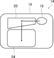
- FIG. 1 is a front view, which is a view of the image display device 10 as viewed from the observation side by the user U.
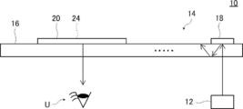
- FIG. 2 is a top view, and is a view of the image display device 10 as viewed from above on the paper surface of FIG.
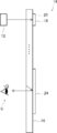
- FIG. 3 is a side view, and is a view of the image display device 10 as viewed from the right-hand side of the paper surface of FIG.
- the image display device 10 shown in FIG. 1 is used as an AR glass as a suitable example.
- the light guide element of the present invention can also be used for optical elements such as transparent screens, lighting devices (including backlights of liquid crystal displays), and sensors. Further, the image display device of the present invention can also be used for an image display device using these optical elements.
- the image display device 10 shown in FIGS. 1 to 3 has a display element 12, a light guide plate 16, and a guide having an incident diffraction element 18, an intermediate diffraction element 20, and an emission diffraction element 24 provided on the light guide plate 16. It has an optical element 14. Note that the display element 12 is not shown in FIG.
- the incident diffraction element 18, the intermediate diffraction element 20, and the outgoing diffraction element 24 are arranged at different positions in the surface direction of the main surface of the light guide plate 16.
- the intermediate diffraction element 20 is arranged on the left side of FIG. 1 of the incident diffraction element 18, and the exit diffraction element 24 is arranged on the lower side of FIG. 1 of the intermediate diffraction element 20.
- the main surface is the maximum surface of a sheet-like object (plate-like object, film, etc.).
- the image display device 10 diffracts the image (light corresponding to the image) displayed by the display element 12 by the incident diffraction element 18 and incidents it on the light guide plate 16. At that time, the incident diffraction element 18 diffracts the light in the direction in which the traveling direction of the diffracted light is toward the intermediate diffraction element 20. In the example shown in FIG. 1, the incident diffraction element 18 diffracts the incident light toward the left in FIG.
- the diffracted light from the incident diffraction element 18 is totally reflected inside the light guide plate 16 and propagated, and is incident on the intermediate diffraction element 20.
- the intermediate diffraction element 20 diffracts the light so that the traveling direction of the incident light is directed toward the exit diffraction element 24. In the example shown in FIG. 1, the intermediate diffraction element 20 diffracts the incident light in the downward direction in FIG.
- the light diffracted by the intermediate diffraction element 20 is totally reflected in the light guide plate 16 and propagated, and is incident on the exit diffraction element 24.
- the emission diffraction element 24 diffracts the incident light so as to deviate from the angle totally reflected inside the light guide plate 16.
- the exit diffraction element 24 diffracts the incident light in the direction perpendicular to the paper surface in FIG. That is, as shown in FIG. 2, the exit diffraction element 24 diffracts the incident light in a direction substantially perpendicular to the main surface of the light guide plate.
- the light diffracted by the exit diffraction element 24 is emitted from the light guide plate 16 and is emitted toward the user U.
- the image display device 10 can display the image irradiated by the display element 12.
- the light guide element 14 has the intermediate diffraction element 20
- the emission pupil is enlarged by diffracting a part of the light at a plurality of places of the intermediate diffraction element. be able to.
- the incident diffraction element, the intermediate diffraction element, and the exit diffraction element are diffraction elements having a liquid crystal layer formed by using a composition containing a liquid crystal compound, and the liquid crystal layer is a diffraction element.
- the bright part and the dark part derived from the liquid crystal phase are inclined with respect to the main surface of the liquid crystal layer, and the normal direction of the line formed by the bright part or the dark part from the bright part to the bright part or from the dark part to the dark part. If the pitch in the incident diffraction element is P in and the pitch in the intermediate diffraction element is P e , then P in ⁇ P e is satisfied.
- the optical axis 40A derived from the liquid crystal compound 40 is a so-called slow-phase axis having the highest refractive index in the liquid crystal compound 40.
- the optic axis 40A is along the long axis direction of the rod shape.
- the optical axis 40A derived from the liquid crystal compound 40 is also referred to as "optical axis 40A of the liquid crystal compound 40" or "optical axis 40A”.
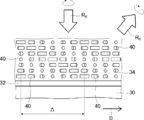
- FIG. 4 is a schematic view showing the orientation state of the liquid crystal compound in the plane of the main surface of the liquid crystal layer 34.
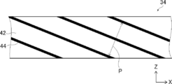
- FIG. 5 is a schematic cross-sectional view showing a state of the liquid crystal phase in a cross section perpendicular to the main surface.
- the main surface of the liquid crystal layer 34 will be referred to as an XY plane, and the cross section perpendicular to the XY plane will be referred to as an XY plane. That is, FIG. 4 corresponds to a schematic view of the XY plane of the liquid crystal layer 34, and FIG.
- the diffraction element has a support 30, an alignment film 32, and a liquid crystal layer 34.
- the liquid crystal layer shown in FIGS. 4 to 6 is an example of a cholesteric liquid crystal layer in which the liquid crystal compound is cholesterically oriented. Further, it is an example when the liquid crystal compound is a rod-shaped liquid crystal compound.
- the liquid crystal layer 34 has a spiral structure in which liquid crystal compounds 40 are spirally swirled and stacked, similar to the cholesteric liquid crystal layer formed by fixing a normal cholesteric liquid crystal phase.
- the liquid crystal compound 40 spirally swirling once has a structure in which the liquid crystal compounds 40 are stacked at a plurality of pitches, with the configuration in which the liquid crystal compounds 40 are spirally rotated once (rotated 360 °) and stacked as one spiral pitch.
- the cholesteric liquid crystal layer in which the cholesteric liquid crystal phase is fixed has wavelength selective reflectivity.
- the selective reflection wavelength range of the cholesteric liquid crystal layer depends on the length of one spiral pitch described above (pitch P shown in FIG. 6).
- the diffraction element having such a liquid crystal layer has wavelength selectivity and diffracts light having a predetermined wavelength. Therefore, the wavelength of the light reflected (diffracted) by the diffraction element may be appropriately set in the selective reflection wavelength range of the liquid crystal layer by adjusting the spiral pitch P of the liquid crystal layer.
- the liquid crystal compounds 40 are arranged along a plurality of array axes D parallel to each other in the XY plane, and are arranged on the respective array axes D.
- the orientation of the optical axis 40A of the liquid crystal compound 40 changes while continuously rotating in one direction in the plane along the array axis D.
- the array axis D is oriented in the X direction.
- the liquid crystal compounds 40 having the same orientation of the optic axis 40A are oriented at equal intervals.
- the direction of the optical axis 40A of the liquid crystal compound 40 changes while continuously rotating in one direction in the plane along the array axis D 1
- the angle formed by D differs depending on the position in the direction of the array axis D, and the angle formed by the optic axis 40A and the array axis D gradually changes from ⁇ to ⁇ + 180 ° or ⁇ -180 ° along the array axis D. It means that it is. That is, as shown in FIG. 4, the plurality of liquid crystal compounds 40 arranged along the array axis D change while the optical axis 40A rotates by a constant angle along the array axis D.
- the difference in angle between the optical axes 40A of the liquid crystal compounds 40 adjacent to each other in the array axis D direction is preferably 45 ° or less, more preferably 15 ° or less, and further preferably a smaller angle. preferable.
- the optical axis 40A of the liquid crystal compound 40 is intended to be the molecular major axis of the rod-shaped liquid crystal compound.
- the optical axis 40A of the liquid crystal compound 40 is intended to be an axis parallel to the normal direction of the disk-shaped liquid crystal compound with respect to the disk surface.
- the optic axis 40A of the liquid crystal compound 40 rotates 180 ° in the arrangement axis D direction in which the optic axis 40A continuously rotates and changes in the plane.
- the length (distance) to be performed be the length ⁇ of one cycle in the liquid crystal alignment pattern. That is, the distance between the centers of the two liquid crystal compounds 40 having the same angle with respect to the array axis D direction in the array axis D direction is defined as the length ⁇ of one cycle.
- the distance between the centers of the two liquid crystal compounds 40 in which the direction of the arrangement axis D and the direction of the optical axis 40A coincide with each other in the direction of the arrangement axis D is the length ⁇ of one cycle. And. In the following description, the length ⁇ of this one cycle is also referred to as "one cycle ⁇ ".
- the liquid crystal alignment pattern of the liquid crystal layer 34 repeats this one cycle ⁇ in one direction in which the direction of the array axis D, that is, the direction of the optic axis 40A continuously rotates and changes.
- the liquid crystal compound 40 forming the liquid crystal layer 34 is in the direction orthogonal to the arrangement axis D direction (Y direction in FIG. 4), that is, in the Y direction orthogonal to one direction in which the optical axis 40A continuously rotates.
- the directions of the optical axes 40A are equal.
- the liquid crystal compound 40 forming the liquid crystal layer 34 has the same angle formed by the optical axis 40A of the liquid crystal compound 40 and the arrow X direction in the Y direction.
- the arrangement direction in which the bright portions 42 and the dark portions 44 are alternately arranged as shown in FIG. 6 is the main plane (XY plane).
- a striped pattern that is inclined at a predetermined angle is observed.
- the distance between the adjacent bright portion 42 to the bright portion 42 or the dark portion 44 to the dark portion 44 in the normal direction of the line formed by the bright portion 42 or the dark portion 44 corresponds to 1/2 pitch. That is, as shown by P in FIG. 6, two bright portions 42 and two dark portions 44 correspond to one pitch of the spiral (one winding number of the spiral).
- the spiral axis derived from the cholesteric liquid crystal phase is perpendicular to the main surface (XY plane), and its reflecting surface is a plane parallel to the main surface (XY plane).
- the optical axis of the liquid crystal compound is not inclined with respect to the main surface (XY plane).
- the optic axis is parallel to the main plane (XY plane). Therefore, when the XX plane of the conventional cholesteric liquid crystal layer is observed by SEM, the arrangement direction in which the bright portion and the dark portion are alternately arranged is perpendicular to the main plane (XY plane). Since the cholesteric liquid crystal phase is specularly reflective, for example, when light is incident on the cholesteric liquid crystal layer from the normal direction, the light is reflected in the normal direction.
- the liquid crystal layer 34 reflects the incident light at an angle in the array axis D direction with respect to specular reflection.
- the liquid crystal layer 34 has a liquid crystal orientation pattern in which the optical axis 40A changes while continuously rotating along the arrangement axis D direction (a predetermined one direction) in the plane.
- the liquid crystal layer 34 as a cholesteric liquid crystal layer that selectively reflects right-circularly polarized light R R of the red light. Therefore, when light is incident on the liquid crystal layer 34, liquid crystal layer 34 reflects only right circularly polarized light R R of the red light, and transmits light of other wavelengths.
- the optical axis 40A of the liquid crystal compound 40 changes while rotating along the array axis D direction (one direction).
- the liquid crystal alignment pattern formed on the liquid crystal layer 34 is a periodic pattern in the arrangement axis D direction. Therefore, the right circularly polarized light R R of the red light incident on the liquid crystal layer 34, as conceptually shown in FIG. 7, is reflected in the direction corresponding to the period of the liquid crystal orientation pattern (diffraction), the reflected red light right circularly polarized light R R is reflected (diffracted) in a direction inclined to the array axis direction D with respect to the XY plane (major surface of the cholesteric liquid crystal layer).
- liquid crystal layer 34 when the liquid crystal layer 34 is applied to a light guide element or the like, light incident from a direction perpendicular to the main surface of the light guide plate can be reflected (diffused) at an angle totally reflected inside the light guide plate.
- the light that is totally reflected inside the light guide plate and guided can be used as a diffraction element that can reflect (diffuse) the light in the direction perpendicular to the main surface of the light guide plate.
- the light reflection direction (diffraction angle) can be adjusted by appropriately setting the array axis D direction, which is one direction in which the optic axis 40A rotates.
- the reflection direction of the circularly polarized light can be reversed by reversing the rotation direction of the optical axis 40A of the liquid crystal compound 40 toward the arrangement axis D direction. ..
- the rotation direction of the optical axis 40A toward the arrangement axis D direction is clockwise, and a certain circularly polarized light is reflected by tilting it in the arrangement axis D direction, which is counterclockwise.
- a certain circularly polarized light is reflected by tilting in the direction opposite to the direction of the array axis D.
- the reflection direction is reversed depending on the spiral turning direction of the liquid crystal compound 40, that is, the turning direction of the reflected circularly polarized light.
- the spiral turning direction of the liquid crystal compound 40 that is, the turning direction of the reflected circularly polarized light.
- the optical axis 40A has a liquid crystal alignment pattern that rotates clockwise along the arrangement axis D direction to the right. Circularly polarized light is reflected by tilting it in the direction of the array axis D.
- the left circularly polarized light is selectively reflected, and the liquid crystal layer has a liquid crystal orientation pattern in which the optical axis 40A rotates clockwise along the arrangement axis D direction. Reflects the left circularly polarized light tilted in the direction opposite to the arrangement axis D direction.
- the length of rotation of the optic axis of the liquid crystal compound by 180 ° is one cycle ⁇ of the diffraction structure, and the optical axis of the liquid crystal compound changes in one direction while rotating (
- the arrangement axis D direction) is the periodic direction of the diffraction structure.
- the shorter one cycle ⁇ the larger the angle of the reflected light with respect to the incident light. That is, the shorter one cycle ⁇ is, the more the reflected light can be tilted and reflected with respect to the incident light.
- the incident diffraction element 18, the intermediate diffraction element 20, and the exit diffraction element 24 have the above-mentioned liquid crystal alignment pattern, and the bright and dark areas observed in the cross section of the SEM.
- the incident diffraction element 18, the intermediate diffraction element 20, and the exit diffraction element 24 reflect (diffract) light of the same wavelength, but in the light guide element of the present invention, compared with the pitch Pin in the incident diffraction element 18. Therefore, the pitch P e in the intermediate diffraction element 20 is large. Further, preferably, the pitch P e of the intermediate diffraction element 20 is larger than the pitch P out of the exit diffraction element 24.
- FIG. 8 shows a conceptual front view for explaining the arrangement of the diffraction elements in the light guide element.
- the liquid crystal layer diffracts the light by reflecting the light in the direction along the arrangement axis D of the liquid crystal alignment pattern. Therefore, as shown in FIG. 8, the incident diffraction element 18 is arranged so that the direction of the array axis D in faces the direction of the intermediate diffraction element 20 so that the diffracted light faces the direction of the intermediate diffraction element 20. ..
- the array axes D in of the incident diffraction element 18 are arranged so as to be parallel in the left-right direction.
- the direction of the arrangement axis D out is the intermediate diffraction element 20 so that the light guided in the light guide plate 16 from the intermediate diffraction element 20 side is directed toward the light emitted from the light guide plate 16. It is arranged so as to face the direction of.
- the array axes D out of the exit diffraction element 24 are arranged so as to be parallel in the vertical direction.
- the intermediate diffraction element 20 diffracts the light so that the traveling direction of the light that is totally reflected and guided in the light guide plate 16 changes in the plane direction.
- the intermediate diffraction element 20 diffracts the light traveling in the left direction in the figure so as to travel in the downward direction in the figure. Therefore, as shown in FIG. 8, the direction of the array axis D e of the intermediate diffractive element 20 is arranged so as to intersect with the traveling direction at a predetermined angle of incident light.
- the intermediate diffraction element 20 the traveling direction of the diffracted light, so that the direction intersecting the direction of the alignment axis D e of the intermediate diffractive element 20 diffracts the light.
- the direction of the array axis D e of the intermediate diffraction element 20 the direction of the array axis D in the input diffraction element 18, and are arranged so as to intersect with the direction of the alignment axis D out of exit diffraction element 24.
- the angle between the alignment axis D in the perpendicular line and the input diffraction element 18 with respect to array axis D e of the intermediate diffractive element 20, the array axis D out of the perpendicular line and the exit diffraction element 24 with respect to array axis D e of the intermediate diffractive element 20 It substantially coincides with the angle of formation ( ⁇ in FIG. 8). Assuming that this angle ⁇ is the rotation angle, the rotation angle ⁇ can be set by adjusting one cycle ⁇ e of the diffraction structure of the intermediate diffraction element 20.
- one cycle ⁇ e of the diffraction structure of the intermediate diffraction element 20 is substantially the same as one cycle ⁇ in of the diffraction structure of the incident diffraction element 18 and one cycle ⁇ out of the diffraction structure of the exit diffraction element 24.
- the rotation angle ⁇ is about 60 ° (see FIG. 9)
- one cycle ⁇ e of the diffraction structure of the intermediate diffraction element 20 is one cycle ⁇ in of the diffraction structure of the incident diffraction element 18, and the diffraction of the emission diffraction element 24.
- the smaller the period ⁇ out of the structure the smaller the rotation angle ⁇ .
- the wavelength of the light that the intermediate diffraction element is reflected at a high efficiency, and short shifts, reflection efficiency is increased for a short wavelength light than has been the selective reflection wavelength in pitches P e, the pitch P e
- the reflection efficiency for light of the selective reflection wavelength set in is low. This causes a problem that the light utilization efficiency of the light guide element becomes low and the displayed image becomes dark.
- the pitch P e in the intermediate diffraction element is larger than the pitch P in in the incident diffraction element and the pitch P out in the exit diffraction element.
- the pitch P e in the intermediate diffractive element setting the pitch P e in the intermediate diffractive element.
- the pitch P e in the intermediate diffraction element larger than the pitch P in in the incident diffraction element, the light reflection efficiency with respect to the selective reflection wavelength of the incident diffraction element and the exit diffraction element can be adjusted to the pitch P e in the intermediate diffraction element. Can be higher than when is the same as the pitch P in in the incident diffraction element. As a result, it is possible to increase the efficiency of light utilization and prevent the displayed image from becoming dark.
- the pitch P out of the outgoing diffraction element is basically the same as the pitch P in of the incident diffraction element from the viewpoint of reflecting light of the same wavelength, but it may be different.
- the pitch P e of the intermediate diffraction element is preferably 1.03 times to 1.5 times, more preferably 1.05 times to 1.4 times, and 1.1 times to 1.1 times the pitch P in of the incident diffraction element. 1.3 times is more preferable.
- the range of the rotation angle ⁇ is not particularly limited, but from the viewpoint of the size of the light guide element and the like, 20 ° to 80 ° is preferable, 30 ° to 65 ° is more preferable, and 40 to 50 ° is further preferable.
- One cycle ⁇ in of the diffraction structure of the incident diffraction element, one cycle ⁇ e of the diffraction structure of the intermediate diffraction element , and one cycle ⁇ out of the diffraction structure of the exit diffraction element are the wavelength of the incident light and the position of each diffraction element. It may be set as appropriate according to the relationship and the like.
- the one cycle ⁇ in of the diffraction structure of the incident diffraction element, the one cycle ⁇ e of the diffraction structure of the intermediate diffraction element , and the one cycle ⁇ out of the diffraction structure of the exit diffraction element are preferably 0.1 ⁇ m to 1 ⁇ m. It is more preferably 0.13 ⁇ m to 0.8 ⁇ m, and even more preferably 0.15 ⁇ m to 0.7 ⁇ m. Further, one cycle ⁇ in of the diffraction structure of the incident diffractive element, one cycle ⁇ e of the diffractive structure of the intermediate diffractive element , and one cycle ⁇ out of the diffractive structure of the outgoing diffractive element propagate the light through the light guide plate by total reflection. It is more preferable that the wavelength of the incident light is ⁇ or less from the viewpoint of causing the light to diffract.
- one cycle ⁇ in of the diffraction structure of the incident diffraction element, one cycle ⁇ e of the diffraction structure of the intermediate diffraction element , and one cycle ⁇ out of the diffraction structure of the exit diffraction element are ⁇ e ⁇ ⁇ in , and ⁇ . It is preferable to satisfy e ⁇ ⁇ out.
- the rotation angle ⁇ can be made smaller, thereby effectively expanding the exit pupil and reducing the size of the light guide element. be able to.
- each diffraction element using the liquid crystal layer may have two or more liquid crystal layers. That is, each diffraction element may be a laminate having a plurality of liquid crystal layers described above.
- the diffraction element When the diffraction element is a laminate having a plurality of liquid crystal layers, the plurality of liquid crystal layers have a configuration in which the formation period of the bright part and the dark part in the cross section of the liquid crystal layer observed by SEM, that is, the pitch P is different. can do. That is, the diffraction element may be configured such that a plurality of liquid crystal layers selectively reflect light having different wavelengths.
- the diffractive element may have two liquid crystal layers, that is, a liquid crystal layer that selectively reflects red light and a liquid crystal layer that selectively reflects green light, and the liquid crystal layer that selectively reflects red light. It may have three liquid crystal layers, that is, a liquid crystal layer that selectively reflects green light and a liquid crystal layer that selectively reflects blue light.
- the diffraction element is a laminated body having a plurality of liquid crystal layers
- one cycle ⁇ of the liquid crystal orientation pattern in each liquid crystal layer is different.
- the plurality of liquid crystal layers differ in the formation period of the bright portion and the dark portion in the cross section of the liquid crystal layer, that is, the pitch P, and the in-plane one cycle ⁇ in the liquid crystal alignment pattern is different, and the length of the pitch P is different.
- the permutation of is the same as the permutation of the length of one cycle ⁇ .
- one cycle in the liquid crystal orientation pattern of the first liquid crystal layer is ⁇ 1, and the liquid crystal orientation pattern of the second liquid crystal layer.
- one cycle in the liquid crystal orientation pattern of the third liquid crystal layer is ⁇ 3, the pitch of the first liquid crystal layer is P1, the pitch of the second liquid crystal layer is P2, and the pitch of the third liquid crystal layer is P3.
- ⁇ 1 ⁇ 2 ⁇ 3, and P1 ⁇ P2 ⁇ P3 are preferably satisfied.
- the intermediate diffraction element and the exit diffraction element is preferably satisfied.
- the diffraction element has a plurality of liquid crystal layers, the light reflected by each liquid crystal layer can be reflected in the same direction by setting the one cycle ⁇ of each liquid crystal layer and the pitch P in the above relationship.
- the light guide element may be configured to reflect three colors of light, red light, green light, and blue light, respectively. , A color image can be guided.
- the diffractive element has three liquid crystal layers having different selective reflection center wavelengths, and has one or two colors selected from visible light such as red light, green light, and blue light, and infrared rays and / or. It may be configured to reflect ultraviolet rays, or may be configured to reflect only light other than visible light.
- the diffraction element may have two or four or more liquid crystal layers having different selective reflection center wavelengths.
- the diffractive element may be configured to reflect light other than visible light such as infrared light and / or ultraviolet light in addition to visible light such as red light, green light and blue light, or each liquid crystal layer may be composed of infrared light and light. / Or a configuration that reflects light other than visible light such as ultraviolet light may be used.
- an image display device 10b having a configuration including two light guide elements, a light guide element 14a and a light guide element 14b, is exemplified.
- one light guide element 14a has a light guide plate 16a, an incident diffraction element 18a provided on the light guide plate 16a, an intermediate diffraction element 20a, and an exit diffraction element 24a, and the other light guide.
- the element 14b includes a light guide plate 16b, an incident diffraction element 18b provided on the light guide plate 16b, an intermediate diffraction element 20b, and an emission diffraction element 24b.
- each diffraction element of the light guide element 14a has a liquid crystal layer that reflects green light
- each diffraction element of the light guide element 14b reflects a liquid crystal layer that reflects blue light and red light.
- the configuration has a liquid crystal layer. With such a configuration, the image display device 10b can guide red light, green light, and blue light, respectively.
- a configuration that reflects two colors selected from red light, green light, and blue light, and one color selected from red light, green light, and blue light, or infrared rays or ultraviolet rays It may be configured to reflect and, or it may be configured to reflect only light other than visible light. Alternatively, for example, it may have three light guide elements, that is, a light guide element for a red image, a light guide element for a green image, and a light guide element for a blue image. That is, the image display device may be configured to have a light guide element for each color.
- a first light guide element having a first light guide plate and a second light guide plate and having a first liquid crystal layer and a third liquid crystal layer provided on the first light guide plate.
- a second liquid crystal layer provided on the second light guide plate
- one cycle in the liquid crystal alignment pattern of the first liquid crystal layer is ⁇ 1
- one cycle in the liquid crystal alignment pattern of the second liquid crystal layer is ⁇ 2
- a third liquid crystal is preferable to satisfy ⁇ 1 ⁇ 2 ⁇ 3.
- P1 ⁇ P2 ⁇ P3 is satisfied when the pitch of the first liquid crystal layer is P1, the pitch of the second liquid crystal layer is P2, and the pitch of the third liquid crystal layer is P3.
- the first light guide element has a first liquid crystal layer that reflects blue light and a third liquid crystal layer that reflects red light
- the second light guide element has a second liquid crystal layer that reflects green light.
- blue light, green light, and red light can be reflected in substantially the same direction.
- the incident diffraction element 18, the intermediate diffraction element 20, and the outgoing diffraction element 24 are bonded to the light guide plate by a bonding layer.
- the bonding layer a layer made of various known materials can be used as long as it is a layer capable of bonding objects to be bonded to each other.
- the bonding layer has fluidity when bonded, and then becomes a solid.
- Even a layer made of an adhesive is a soft solid gel-like (rubber-like) when bonded, and is subsequently gel-like. It may be a layer made of a pressure-sensitive adhesive whose state does not change, or a layer made of a material having the characteristics of both an adhesive and a pressure-sensitive adhesive. Therefore, the bonding layer is used for bonding sheet-like objects such as optical transparent adhesives (OCA (Optical Clear Adhesive)), optical transparent double-sided tape, and ultraviolet curable resins in optical devices and optical elements.
- OCA optical Clear Adhesive
- a known layer may be used.
- the incident diffraction element 18, the intermediate diffraction element 20, the exit diffraction element 24, and the light guide plate 16 are laminated and held by a frame or a jig, according to the present invention.
- a light guide element may be configured.
- the incident diffraction element 18, the intermediate diffraction element 20, and the outgoing diffraction element 24 may be formed directly on the light guide plate 16.
- the display element 12 displays an image (video) observed by the user U and irradiates the incident diffraction element 18 with the image. Therefore, the display element 12 is arranged so that the image to be irradiated is incident on the incident diffraction element 18. In the examples shown in FIGS. 1 to 3, the display element 12 is arranged so as to face the incident diffraction element 18.
- the display element 12 is not limited, and various known display elements (display devices, projectors) used for AR glasses and the like can be used.
- display element 12 a display element having a display and a projection lens is exemplified.
- the display is not limited, and various known displays used for, for example, AR glasses can be used.
- the display include a liquid crystal display (LCOS: including Liquid Crystal On Silicon), an organic electroluminescence display, and a scanning display using a DLP (Digital Light Processing) or MEMS (Micro Electro Mechanical Systems) mirror. Is exemplified.
- each diffractive element has a plurality of liquid crystal layers having different selective reflection wavelengths
- a display that displays a multicolor image using light having a wavelength reflected by each liquid crystal layer is used. Further, as shown in FIG. 10, even when a plurality of light guide elements are provided, a display that displays a multicolor image using light having a wavelength reflected by the liquid crystal layer of each diffraction element of each light guide element is used. ..
- the projection lens is also a known projection lens (colimating lens) used for AR glasses and the like.
- the display image by the display element 12 that is, the light emitted by the display element 12 is not limited, but polarized light, particularly circularly polarized light, is preferable.
- the display element 12 irradiates a circularly polarized light and the display irradiates an unpolarized image
- the display element 12 preferably has, for example, a circularly polarizing plate composed of a linear polarizing element and a ⁇ / 4 plate. ..
- the display element 12 when the display illuminates a linearly polarized image, the display element 12 preferably has, for example, a ⁇ / 4 plate.
- the light emitted by the display element 12 may be other polarized light (for example, linearly polarized light).
- the light guide plate 16 is a known light guide plate that reflects light incident on the inside and guides (propagates) the light.
- the light guide plate 16 is not limited, and various known light guide plates used in AR glasses, backlight units of liquid crystal displays, and the like can be used.
- the incident diffraction element 18, the intermediate diffraction element 20, and the exit diffraction element 24 basically have the same configuration except that the pitch P of the liquid crystal layer, one cycle ⁇ of the diffraction structure, the arrangement position on the light guide plate, and the like are different. Therefore, in the following description, when it is not necessary to distinguish between the incident diffraction element 18, the intermediate diffraction element 20, and the exit diffraction element 24, they are collectively referred to as a diffraction element.
- the diffractive element is formed by using the composition containing the liquid crystal compound, and the direction of the optical axis derived from the liquid crystal compound is changed while continuously rotating along at least one direction in the plane. It has a pattern and has a liquid crystal layer in which the bright and dark parts derived from the liquid crystal phase are inclined with respect to the main surface in the cross section observed by SEM.
- the configuration of the liquid crystal layer is as described above.
- the liquid crystal compound 40 has a configuration in which the optical axis 40A is oriented parallel to the main surface (XY plane) on the XX plane of the liquid crystal layer 34.
- the liquid crystal compound 40 is oriented with its optical axis 40A inclined with respect to the main plane (XY plane). There may be.
- the inclination angle (tilt angle) with respect to the main plane (XY plane) of the liquid crystal compound 40 is uniform in the thickness direction (Z direction).
- the liquid crystal layer 34 may have regions in which the tilt angles of the liquid crystal compounds 40 are different in the thickness direction.
- the optical axis 40A of the liquid crystal compound 40 is parallel to the main surface (the pretilt angle is 0) at the interface on the alignment film 32 side of the liquid crystal layer, and from the interface on the alignment film 32 side.
- the tilt angle of the liquid crystal compound 40 increases as the distance from the liquid crystal compound 40 increases, and then the liquid crystal compound is oriented at a constant tilt angle to the other interface (air interface) side.
- the optical axis of the liquid crystal compound may have a pretilt angle at one interface of the upper and lower interfaces, or may have a pretilt angle at both interfaces. Good. Further, the pretilt angle may be different at both interfaces. Since the liquid crystal compound has a tilt angle (tilt) in this way, the birefringence of the liquid crystal compound that is effective when light is diffracted becomes high, and the diffraction efficiency can be improved.
- the average angle (average tilt angle) formed by the optical axis 40A of the liquid crystal compound 40 and the main surface (XY plane) is preferably 5 to 80 °, more preferably 10 to 50 °.
- the average tilt angle can be measured by observing the XX plane of the liquid crystal layer 34 with a polarizing microscope. Above all, on the XX plane of the liquid crystal layer 34, it is preferable that the optical axis 40A of the liquid crystal compound 40 is inclined or oriented in the same direction with respect to the main plane (XY plane).
- the tilt angle is a value obtained by measuring the angle formed by the optical axis 40A of the liquid crystal compound 40 and the main surface at any five or more points in the polarization microscope observation of the cross section of the cholesteric liquid crystal layer and arithmetically averaging them. is there.
- liquid crystal layer Light vertically incident on the diffraction element (liquid crystal layer) travels diagonally in the liquid crystal layer due to the application of bending force.
- a diffraction loss occurs because the deviation from the conditions such as the diffraction period originally set so as to obtain a desired diffraction angle with respect to the vertical incident occurs.
- the liquid crystal compound is tilted, there is an orientation in which a higher birefringence is generated with respect to the orientation in which the light is diffracted, as compared with the case where the liquid crystal compound is not tilted.
- the effective abnormal light refractive index becomes large, so that the birefringence, which is the difference between the abnormal light refractive index and the normal light refractive index, becomes high.
- the direction of the tilt angle according to the target diffraction direction, it is possible to suppress the deviation from the original diffraction condition in that direction, and as a result, a liquid crystal compound having a tilt angle was used. In this case, it is considered that higher diffraction efficiency can be obtained.
- the tilt angle is controlled by the treatment of the interface of the liquid crystal layer.
- the tilt angle of the liquid crystal compound can be controlled by performing a pre-tilt treatment on the alignment film. For example, when the alignment film is formed, the alignment film is exposed to ultraviolet rays from the front and then obliquely exposed to cause a pretilt angle in the liquid crystal compound in the liquid crystal layer formed on the alignment film. In this case, the liquid crystal compound is pre-tilted in a direction in which the uniaxial side of the liquid crystal compound can be seen with respect to the second irradiation direction.
- liquid crystal compound in the direction perpendicular to the second irradiation direction does not pre-tilt, there are an in-plane pre-tilt region and a non-pre-tilt region. This contributes to increasing the birefringence most in that direction when the light is diffracted in the target direction, and is therefore suitable for increasing the diffraction efficiency.
- an additive that promotes the pretilt angle can be added in the liquid crystal layer or the alignment film. In this case, an additive can be used as a factor for further increasing the diffraction efficiency. This additive can also be used to control the pretilt angle of the interface on the air side.
- the bright part and the dark part derived from the cholesteric liquid crystal phase are inclined with respect to the main surface.
- the liquid crystal layer has the minimum in-plane retardation Re in either the slow-phase axial plane or the advancing axial plane.
- the direction is inclined from the normal direction.
- the absolute value of the measurement angle formed by the normal in the direction in which the in-plane retardation Re is minimized is 5 ° or more.
- the liquid crystal compound of the liquid crystal layer is inclined with respect to the main surface, and the inclination direction substantially coincides with the bright part and the dark part of the liquid crystal layer.
- the normal direction is a direction orthogonal to the main surface. Since the liquid crystal layer has such a configuration, circularly polarized light can be diffracted with higher diffraction efficiency than the liquid crystal layer in which the liquid crystal compound is parallel to the main surface.
- the liquid crystal compound of the liquid crystal layer is inclined with respect to the main surface and the inclination direction substantially coincides with the bright part and the dark part
- the bright part and the dark part corresponding to the reflecting surface and the optical axis of the liquid crystal compound are aligned. Match. Therefore, the action of the liquid crystal compound on the reflection (diffraction) of light is increased, and the diffraction efficiency can be improved. As a result, the amount of reflected light with respect to the incident light can be further improved.
- the absolute value of the optical axis tilt angle of the liquid crystal layer is preferably 5 ° or more, more preferably 15 ° or more, still more preferably 20 ° or more.
- the absolute value of the optical axis tilt angle is preferably 5 ° or more, more preferably 15 ° or more, still more preferably 20 ° or more.
- the diffraction element has a structure including a support 30, an alignment film 32, and a liquid crystal layer 34, but the diffraction element is not limited thereto.
- the diffraction element may be configured to have only the alignment film 32 and the liquid crystal layer 34 by peeling off the support 30 after being attached to the light guide plate 16.
- the diffraction element may be configured to have only the liquid crystal layer 34 by peeling off the support 30 and the alignment film 32 after being attached to the light guide plate 16, for example.
- the support 30 supports the alignment film 32 and the liquid crystal layer 34.
- various sheet-like materials films, plate-like materials
- the support 30 has a transmittance of 50% or more, more preferably 70% or more, and further preferably 85% or more with respect to the corresponding light.
- the thickness of the support 30 is not limited, and the thickness capable of holding the alignment film 32 and the liquid crystal layer 34 may be appropriately set according to the use of the diffraction element, the material for forming the support 30, and the like.
- the thickness of the support 30 is preferably 1 to 2000 ⁇ m, more preferably 3 to 500 ⁇ m, and even more preferably 5 to 250 ⁇ m.
- the support 30 may be single-layered or multi-layered.
- Examples of the support 30 in the case of a single layer include a support 30 made of glass, triacetyl cellulose (TAC), polyethylene terephthalate (PET), polycarbonate, polyvinyl chloride, acrylic, polyolefin or the like.
- Examples of the support 30 in the case of a multi-layer structure include those including any of the above-mentioned single-layer supports as a substrate and providing another layer on the surface of the substrate.
- an alignment film 32 is formed on the surface of the support 30.
- the alignment film 32 is an alignment film for orienting the liquid crystal compound 40 in a predetermined liquid crystal alignment pattern when forming the liquid crystal layer 34.
- the liquid crystal layer 34 is a liquid crystal in which the orientation of the optical axis 40A (see FIG. 4) derived from the liquid crystal compound 40 is continuously rotated along one direction in the plane. It has an orientation pattern. Therefore, the alignment film 32 is formed so that the liquid crystal layer 34 can form this liquid crystal alignment pattern.
- “the direction of the optic axis 40A rotates” is also simply referred to as "the optical axis 40A rotates”.
- a rubbing-treated film made of an organic compound such as a polymer an oblique vapor-deposited film of an inorganic compound, a film having a microgroove, and Langmuir of an organic compound such as ⁇ -tricosanoic acid, dioctadecylmethylammonium chloride and methyl stearylate.
- An example is a film obtained by accumulating LB (Langmuir-Blodgett) films produced by the Brodget method.
- the alignment film 32 by the rubbing treatment can be formed by rubbing the surface of the polymer layer with paper or cloth several times in a certain direction.
- Materials used for the alignment film 32 include polyimide, polyvinyl alcohol, polymers having a polymerizable group described in JP-A-9-152509, JP-A-2005-97377, JP-A-2005-99228, and JP-A-2005-99228. , JP-A-2005-128503, the material used for forming the alignment film 32 and the like described in JP-A-2005-128503 is preferable.
- a so-called photo-alignment film which is obtained by irradiating a photo-alignable material with polarized light or non-polarized light to form an alignment film 32, is preferably used. That is, as the alignment film 32, a photoalignment film formed by applying a photoalignment material on the support 30 is preferably used. Polarized light irradiation can be performed from a vertical direction or an oblique direction with respect to the photoalignment film, and non-polarized light irradiation can be performed from an oblique direction with respect to the photoalignment film.
- Examples of the photoalignment material used for the alignment film that can be used in the present invention include JP-A-2006-285197, JP-A-2007-76839, JP-A-2007-138138, and JP-A-2007-94071. , JP-A-2007-121721, JP-A-2007-140465, JP-A-2007-156439, JP-A-2007-133184, JP-A-2009-109831, Patent No. 3883848 and Patent No. 4151746.
- the azo compound described in JP-A the aromatic ester compound described in JP-A-2002-229039, the maleimide having the photoorientation unit described in JP-A-2002-265541 and JP-A-2002-317013, and / Alternatively, an alkenyl-substituted nadiimide compound, a photobridgeable silane derivative described in Japanese Patent No. 4205195 and Patent No. 4205198, a photocrossbable property described in JP-A-2003-520878, JP-A-2004-522220 and Patent No. 4162850.
- Photodimerizable compounds described in Japanese Patent Application Laid-Open No. -177561 and Japanese Patent Application Laid-Open No. 2014-12823, particularly cinnamate compounds, chalcone compounds, coumarin compounds and the like are exemplified as preferable examples.
- azo compounds, photocrosslinkable polyimides, photocrosslinkable polyamides, photocrosslinkable polyesters, synnamate compounds, and chalcone compounds are preferably used.
- the thickness of the alignment film 32 is not limited, and the thickness at which the required alignment function can be obtained may be appropriately set according to the material for forming the alignment film 32.
- the thickness of the alignment film 32 is preferably 0.01 to 5 ⁇ m, more preferably 0.05 to 2 ⁇ m.
- the method for forming the alignment film 32 there is no limitation on the method for forming the alignment film 32, and various known methods depending on the material for forming the alignment film 32 can be used. As an example, a method in which the alignment film 32 is applied to the surface of the support 30 and dried, and then the alignment film 32 is exposed with a laser beam to form an alignment pattern is exemplified.
- FIG. 13 conceptually shows an example of an exposure apparatus that exposes the alignment film 32 to form an alignment pattern.
- the exposure apparatus 60 shown in FIG. 13 uses a light source 64 provided with a laser 62, a ⁇ / 2 plate 65 for changing the polarization direction of the laser beam M emitted by the laser 62, and a light beam MA and the laser beam M emitted by the laser 62. It includes a polarizing beam splitter 68 that separates the MB into two, mirrors 70A and 70B arranged on the optical paths of the two separated rays MA and MB, respectively, and ⁇ / 4 plates 72A and 72B.
- the light source 64 emits linearly polarized light P 0 .
- lambda / 4 plate 72A is linearly polarized light P 0 (the ray MA) to the right circularly polarized light P R
- lambda / 4 plate 72B is linearly polarized light P 0 (the rays MB) to the left circularly polarized light P L, converts respectively.
- the support 30 having the alignment film 32 before the alignment pattern is formed is arranged in the exposed portion, and the two light rays MA and the light rays MB are crossed and interfered with each other on the alignment film 32, and the interference light is made to interfere with the alignment film 32. Is exposed to light. Due to the interference at this time, the polarization state of the light applied to the alignment film 32 periodically changes in the form of interference fringes. As a result, an alignment film having an orientation pattern in which the orientation state changes periodically (hereinafter, also referred to as a pattern alignment film) can be obtained. In the exposure apparatus 60, the period of the orientation pattern can be adjusted by changing the intersection angle ⁇ of the two rays MA and MB.
- the optical axis 40A rotates in one direction.
- the length of one cycle in which the optic axis 40A rotates 180 ° can be adjusted.
- the above-mentioned optical axis 40A derived from the liquid crystal compound 40 is continuously arranged in one direction.
- the liquid crystal layer 34 having a rotating liquid crystal orientation pattern can be formed. Further, the rotation direction of the optical shaft 40A can be reversed by rotating the optical axes of the ⁇ / 4 plates 72A and 72B by 90 °, respectively.
- the pattern alignment film is a liquid crystal in which the direction of the optical axis of the liquid crystal compound in the liquid crystal layer formed on the pattern alignment film changes while continuously rotating along at least one direction in the plane. It has an orientation pattern that orients the liquid crystal compound so that it becomes an orientation pattern. Assuming that the axis of the pattern alignment film is the axis along the direction in which the liquid crystal compound is oriented, the direction of the alignment axis of the pattern alignment film changes while continuously rotating along at least one direction in the plane. It can be said that it has an orientation pattern.
- the orientation axis of the pattern alignment film can be detected by measuring the absorption anisotropy. For example, when the pattern alignment film is irradiated with rotating linearly polarized light and the amount of light transmitted through the pattern alignment film is measured, the direction in which the amount of light becomes maximum or minimum gradually changes along one direction in the plane. It changes and is observed.
- the alignment film 32 is provided as a preferred embodiment and is not an essential constituent requirement.
- the liquid crystal layer has an optical axis 40A derived from the liquid crystal compound 40. It is also possible to have a configuration having a liquid crystal orientation pattern in which the orientation of the liquid crystal is changed while continuously rotating along at least one direction in the plane. That is, in the present invention, the support 30 may act as an alignment film.
- the liquid crystal layer can be formed by fixing the liquid crystal phase in which the liquid crystal compound is oriented in a predetermined orientation state in a layered manner.
- the cholesteric liquid crystal phase can be fixed and formed in layers.
- the structure in which the liquid crystal phase is fixed may be a structure in which the orientation of the liquid crystal compound serving as the liquid crystal phase is maintained, and typically, the polymerizable liquid crystal compound is placed in a predetermined liquid crystal phase orientation state. It is preferable that the structure is polymerized and cured by irradiation with ultraviolet rays, heating, etc.
- the structure is changed to a state in which the orientation form is not changed by an external field or an external force.
- the liquid crystal phase is fixed, it is sufficient that the optical properties of the liquid crystal phase are maintained, and the liquid crystal compound 40 does not have to exhibit liquid crystal properties in the liquid crystal layer.
- the polymerizable liquid crystal compound may lose its liquid crystal property by increasing its molecular weight by a curing reaction.
- liquid crystal composition containing a liquid crystal compound can be mentioned.
- the liquid crystal compound is preferably a polymerizable liquid crystal compound.
- the liquid crystal composition used for forming the liquid crystal layer may further contain a surfactant and a chiral agent.
- the polymerizable liquid crystal compound may be a rod-shaped liquid crystal compound or a disk-shaped liquid crystal compound.
- the rod-shaped polymerizable liquid crystal compound include a rod-shaped nematic liquid crystal compound.
- rod-shaped nematic liquid crystal compounds include azomethines, azoxys, cyanobiphenyls, cyanophenyl esters, benzoic acid esters, cyclohexanecarboxylic acid phenyl esters, cyanophenylcyclohexanes, cyano-substituted phenylpyrimidins, and alkoxy-substituted phenylpyrimidins.
- Phenyldioxans, trans, alkenylcyclohexylbenzonitriles and the like are preferably used. Not only low molecular weight liquid crystal compounds but also high molecular weight liquid crystal compounds can be used.
- the polymerizable liquid crystal compound is obtained by introducing a polymerizable group into the liquid crystal compound.
- the polymerizable group include an unsaturated polymerizable group, an epoxy group, and an aziridinyl group, and an unsaturated polymerizable group is preferable, and an ethylenically unsaturated polymerizable group is more preferable.
- the polymerizable group can be introduced into the molecule of the liquid crystal compound by various methods.
- the number of polymerizable groups contained in the polymerizable liquid crystal compound is preferably 1 to 6, more preferably 1 to 3.
- Examples of polymerizable liquid crystal compounds include Makromol. Chem. , 190, 2255 (1989), Advanced Materials 5, 107 (1993), US Pat. No.
- a cyclic organopolysiloxane compound having a cholesteric phase as disclosed in Japanese Patent Application Laid-Open No. 57-165480 can be used.
- a polymer liquid crystal compound a polymer having a mesogen group exhibiting a liquid crystal introduced at the main chain, a side chain, or both the main chain and the side chain, and a polymer cholesteric having a cholesteryl group introduced into the side chain.
- Liquid crystals, liquid crystal polymers as disclosed in JP-A-9-133810, liquid crystal polymers as disclosed in JP-A-11-293252, and the like can be used.
- disk-shaped liquid crystal compound As the disk-shaped liquid crystal compound, for example, those described in JP-A-2007-108732 and JP-A-2010-244038 can be preferably used.
- the amount of the polymerizable liquid crystal compound added to the liquid crystal composition is preferably 75 to 99.9% by mass, preferably 80 to 99% by mass, based on the solid content mass (mass excluding the solvent) of the liquid crystal composition. It is more preferably mass%, and even more preferably 85-90 mass%.
- the liquid crystal composition used when forming the liquid crystal layer may contain a surfactant.
- the surfactant is preferably a compound capable of stably or rapidly functioning as an orientation control agent that contributes to the orientation of the cholesteric liquid crystal phase.
- examples of the surfactant include silicone-based surfactants and fluorine-based surfactants, and fluorine-based surfactants are preferably exemplified.
- the surfactant include the compounds described in paragraphs [2002] to [0090] of JP2014-119605A, and the compounds described in paragraphs [0031] to [0034] of JP2012-203237A. , The compounds exemplified in paragraphs [0092] and [093] of JP-A-2005-999248, paragraphs [0076] to [0078] and paragraphs [0083] to [0085] of JP-A-2002-129162. Examples thereof include the compounds exemplified therein, and the fluorine (meth) acrylate-based polymers described in paragraphs [0018] to [0043] of JP-A-2007-272185.
- the surfactant one type may be used alone, or two or more types may be used in combination.
- the fluorine-based surfactant the compounds described in paragraphs [2002] to [0090] of JP2014-119605 are preferable.
- the amount of the surfactant added to the liquid crystal composition is preferably 0.01 to 10% by mass, more preferably 0.01 to 5% by mass, and 0.02 to 1% by mass with respect to the total mass of the liquid crystal compound. Is even more preferable.
- the chiral agent has a function of inducing a helical structure of a cholesteric liquid crystal phase. Since the twist direction or spiral pitch of the spiral induced by the compound differs depending on the compound, the chiral agent may be selected according to the purpose.
- the chiral agent is not particularly limited, and is a known compound (for example, Liquid Crystal Device Handbook, Chapter 3, Section 4-3, TN (twisted nematic), STN (Super Twisted Nematic) chiral agent, page 199, Japan Society for the Promotion of Science. (Described in 1989, edited by the 142nd Committee of the Society), isosorbide, isomannide derivatives and the like can be used.
- the chiral agent generally contains an asymmetric carbon atom, but an axial asymmetric compound or a surface asymmetric compound that does not contain an asymmetric carbon atom can also be used as the chiral agent.
- axial or surface asymmetric compounds include binaphthyl, helicene, paracyclophane, and derivatives thereof.
- the chiral agent may have a polymerizable group. When both the chiral agent and the liquid crystal compound have a polymerizable group, the repeating unit derived from the polymerizable liquid crystal compound and the repeating unit derived from the chiral agent are derived by the polymerization reaction between the polymerizable chiral agent and the polymerizable liquid crystal compound. Polymers with repeating units can be formed.
- the polymerizable group of the polymerizable chiral agent is preferably a group of the same type as the polymerizable group of the polymerizable liquid crystal compound. Therefore, the polymerizable group of the chiral agent is preferably an unsaturated polymerizable group, an epoxy group or an aziridinyl group, more preferably an unsaturated polymerizable group, and preferably an ethylenically unsaturated polymerizable group. More preferred. Moreover, the chiral agent may be a liquid crystal compound.
- the chiral auxiliary has a photoisomeric group
- a pattern of a desired reflection wavelength corresponding to the emission wavelength can be formed by irradiation with a photomask such as active light after coating and orientation.
- a photomask such as active light after coating and orientation.
- an isomerization site of a compound exhibiting photochromic properties an azo group, an azoxy group, or a cinnamoyl group is preferable.
- Specific compounds include JP-A-2002-80478, JP-A-2002-80851, JP-A-2002-179668, JP-A-2002-179669, JP-A-2002-179670, and JP-A-2002.
- the content of the chiral agent in the liquid crystal composition is preferably 0.01 to 200 mol%, more preferably 1 to 30 mol%, based on the molar content of the liquid crystal compound.
- the liquid crystal composition contains a polymerizable compound, it preferably contains a polymerization initiator.
- the polymerization initiator used is preferably a photopolymerization initiator capable of initiating the polymerization reaction by irradiation with ultraviolet rays.
- photopolymerization initiators include ⁇ -carbonyl compounds (described in U.S. Pat. No. 2,376,661 and U.S. Pat. No. 2,376,670), acidoin ethers (described in U.S. Pat. No. 2,448,828), and ⁇ -hydrogen.
- Substituted aromatic acidoine compounds (described in US Pat. No. 2722512), polynuclear quinone compounds (described in US Pat. Nos. 3046127 and US Pat. No. 2951758), triarylimidazole dimers and p-aminophenyl ketone. Combinations (described in US Pat. No. 3,549,677), aclysine and phenazine compounds (Japanese Patent Laid-Open No. 60-105667, described in US Pat. No. 4,239,850), and oxadiazole compounds (US Pat. No. 421,970). Description) and the like.
- the content of the photopolymerization initiator in the liquid crystal composition is preferably 0.1 to 20% by mass, more preferably 0.5 to 12% by mass, based on the content of the liquid crystal compound.
- the liquid crystal composition may optionally contain a cross-linking agent in order to improve the film strength and durability after curing.
- a cross-linking agent those that are cured by ultraviolet rays, heat, humidity and the like can be preferably used.
- the cross-linking agent is not particularly limited and may be appropriately selected depending on the intended purpose. For example, a polyfunctional acrylate compound such as trimethylolpropantri (meth) acrylate and pentaerythritol tri (meth) acrylate; glycidyl (meth) acrylate.
- epoxy compounds such as ethylene glycol diglycidyl ether; aziridine compounds such as 2,2-bishydroxymethylbutanol-tris [3- (1-aziridinyl) propionate] and 4,4-bis (ethyleneiminocarbonylamino) diphenylmethane; hexa Isocyanate compounds such as methylene diisocyanate and biuret type isocyanate; polyoxazoline compounds having an oxazoline group in the side chain; and alkoxysilane compounds such as vinyltrimethoxysilane and N- (2-aminoethyl) 3-aminopropyltrimethoxysilane. Can be mentioned.
- a known catalyst can be used depending on the reactivity of the cross-linking agent, and the productivity can be improved in addition to the improvement of the film strength and durability. These may be used alone or in combination of two or more.
- the content of the cross-linking agent is preferably 3 to 20% by mass, more preferably 5 to 15% by mass, based on the solid content mass of the liquid crystal composition. When the content of the cross-linking agent is within the above range, the effect of improving the cross-linking density can be easily obtained, and the stability of the liquid crystal phase is further improved.
- a polymerization inhibitor an antioxidant, an ultraviolet absorber, a light stabilizer, a coloring material, metal oxide fine particles, etc. are added to the liquid crystal composition within a range that does not deteriorate the optical performance and the like. Can be added with.
- the liquid crystal composition is preferably used as a liquid when forming a liquid crystal layer.
- the liquid crystal composition may contain a solvent.
- the solvent is not limited and may be appropriately selected depending on the intended purpose, but an organic solvent is preferable.
- the organic solvent is not limited and may be appropriately selected depending on the intended purpose.
- a liquid crystal composition is applied to the forming surface of the liquid crystal layer, the liquid crystal compound is oriented to a desired liquid crystal phase state, and then the liquid crystal compound is cured to form a liquid crystal layer.
- the liquid crystal composition is applied to the alignment film 32, the liquid crystal compound is oriented in the state of the cholesteric liquid crystal phase, and then the liquid crystal compound is cured to form cholesteric. It is preferable to form a liquid crystal layer in which the liquid crystal phase is fixed.
- printing methods such as inkjet and scroll printing, and known methods such as spin coating, bar coating and spray coating that can uniformly apply the liquid to a sheet-like material can be used.
- the applied liquid crystal composition is dried and / or heated as needed and then cured to form a liquid crystal layer.
- the liquid crystal compound in the liquid crystal composition may be oriented to the cholesteric liquid crystal phase.
- the heating temperature is preferably 200 ° C. or lower, more preferably 130 ° C. or lower.
- the oriented liquid crystal compound is further polymerized, if necessary.
- the polymerization may be either thermal polymerization or photopolymerization by light irradiation, but photopolymerization is preferable.
- the irradiation energy is preferably 20mJ / cm 2 ⁇ 50J / cm 2, more preferably 50 ⁇ 1500mJ / cm 2.
- light irradiation may be carried out under heating conditions or a nitrogen atmosphere.
- the wavelength of the ultraviolet rays to be irradiated is preferably 250 to 430 nm.
- the thickness of the liquid crystal layer is not limited, and the required light reflectance can be obtained depending on the application of the diffraction element, the light reflectance required for the liquid crystal layer, the material for forming the liquid crystal layer, and the like. It may be set as appropriate.
- the liquid crystal layer is a cholesteric liquid crystal layer in which the liquid crystal compound is cholesterically oriented, but the present invention is not limited to this.
- the liquid crystal layer may have a configuration in which the liquid crystal compound is not spirally cholesterically oriented in the thickness direction and the liquid crystal compound has a region in which the liquid crystal compound is twisted and rotated with a twist angle of less than 360 °.
- the present invention is not limited to the above-mentioned examples, and various improvements and changes may be made without departing from the gist of the present invention. Of course, it's good.
- Example 1 ⁇ Manufacturing of incident diffraction element A1> (Formation of alignment film) A glass substrate was prepared as a support. The following coating liquid for forming an alignment film was applied onto the support by spin coating. The support on which the coating film of the coating film for forming the alignment film was formed was dried on a hot plate at 60 ° C. for 60 seconds to form the alignment film.
- Coating liquid for forming an alignment film Materials for photo-alignment below 1.00 parts by mass Water 16.00 parts by mass Butoxyethanol 42.00 parts by mass Propylene glycol monomethyl ether 42.00 parts by mass ⁇ ⁇
- the alignment film was exposed using the exposure apparatus shown in FIG. 13 to form an alignment film P-1 having an alignment pattern.
- a laser that emits laser light having a wavelength (325 nm) was used.
- the exposure amount due to the interference light was set to 1000 mJ / cm 2 .
- One cycle (the length of rotation of the optic axis by 180 °) of the orientation pattern formed by the interference between the two laser beams was controlled by changing the intersection angle (intersection angle ⁇ ) of the two lights.
- composition A-1 was prepared as a liquid crystal composition for forming the incident diffraction element A1.
- This composition A-1 is a liquid crystal composition that forms a cholesteric liquid crystal layer (cholesteric liquid crystal phase) that reflects right-handed circularly polarized light.
- composition A-1 is applied onto the alignment film P-1, the coating film is heated to 80 ° C. on a hot plate, and then the wavelength is 365 nm using a high-pressure mercury lamp at 80 ° C. under a nitrogen atmosphere.
- the coating film By irradiating the coating film with an irradiation amount of 300 mJ / cm 2 , the orientation of the liquid crystal compound was fixed and the liquid crystal layer of the incident diffraction element A1 was formed.
- the number of pitches in the normal direction (thickness direction) with respect to the main surface was 8 pitches.
- the pitch P in of the inclined surface of the bright part and the dark part with respect to the main surface was 0.31 ⁇ m.
- the bright and dark areas referred to here are bright and dark areas derived from the cholesteric liquid crystal phase, which are seen when the cross section of the cholesteric liquid crystal layer is observed by SEM.
- the intermediate diffraction element A1 was produced in the same manner as the incident diffraction element A1 except that the amount of the chiral agent in the composition forming the liquid crystal layer was changed to 4.87 parts by mass and the film thickness was adjusted. did.
- the number of pitches in the thickness direction of the liquid crystal layer of the intermediate diffraction element A1 was 2, and the pitch P e of the liquid crystal layer was 0.39 ⁇ m. Further, in the liquid crystal orientation pattern, one cycle ⁇ e in which the optical axis of the liquid crystal compound was rotated by 180 ° was 0.32 ⁇ m.
- the exit diffraction element A1 was manufactured in the same manner as the incident diffraction element A1 except that the film thickness was adjusted.
- a light guide plate having a size of 55 mm ⁇ 60 mm, a thickness of 1 mm, and a material: glass was used as the light guide plate.
- the incident diffraction element A1 was cut out to a size of 6 mm in diameter and used.
- the intermediate diffraction element A1 was cut out to a size of 15 mm (maximum) ⁇ 30 mm and used.
- the emission diffraction element A1 was cut out to a size of 25 mm ⁇ 30 mm and used.
- the cutting direction and the periodic direction of the diffraction structure are adjusted so that the periodic direction of the diffraction structure becomes a predetermined direction when each diffraction element is arranged on the light guide plate. Cut out.
- Each of the produced diffraction elements was bonded to one main surface of the light guide plate using an adhesive.
- the arrangement of each diffraction element was as shown in FIG.
- the intermediate diffraction element A1 and the incident diffraction element A1 are arranged at a distance of 1 mm in the left-right direction. Further, the exit diffraction element A1 and the intermediate diffraction element A1 are arranged at a distance of 6 mm in the vertical direction. From the above, the light guide element A1 was manufactured.
- the angle formed by the periodic direction of the diffraction structure of the incident diffraction element A1 (direction of the array axis D in ) and the periodic direction of the diffraction structure of the exit diffraction element A1 (direction of the array axis D out ) is It is 120 °. That is, the rotation angle ⁇ formed by the perpendicular line of the intermediate diffraction element A1 with respect to the arrangement axis D e and the arrangement axis D in of the incident diffraction element A1, and the arrangement of the perpendicular line of the intermediate diffraction element A1 with respect to the arrangement axis D e and the exit diffraction element A1.
- the angle of rotation ⁇ formed with the axis D out is 60 °.
- the light guide element B1 was manufactured in the same manner as in Example 1 except that the intermediate diffraction element B1 was manufactured in the same manner as the incident diffraction element A1. That is, the pitch P e of the liquid crystal layer of the intermediate diffraction element B1 was 0.31 ⁇ m. Further, in the liquid crystal orientation pattern, one cycle ⁇ e in which the optical axis of the liquid crystal compound was rotated by 180 ° was 0.32 ⁇ m.
- Example 2 Manufacture of Incident Diffractive Element A2
- the intersection angle (diffraction angle ⁇ ) of the two lights is changed so that one cycle of the alignment pattern formed on the alignment film is different, and the amount of the chiral auxiliary in the composition forming the liquid crystal layer is 5.
- An incident diffraction element A2 was produced in the same manner as the incident diffraction element A1 of Example 1 except that the thickness was changed to .27 parts by mass and the film thickness was adjusted.
- the number of pitches in the thickness direction of the liquid crystal layer of the incident diffraction element A2 was 8 pitches, and in the liquid crystal alignment pattern, one cycle ⁇ in in which the optical axis of the liquid crystal compound was rotated by 180 ° was 0.39 ⁇ m.
- the pitch P in of the liquid crystal layer was 0.36 ⁇ m.
- the number of pitches in the thickness direction of the liquid crystal layer was 2 pitches, and in the liquid crystal orientation pattern, one cycle ⁇ e in which the optical axis of the liquid crystal compound was rotated by 180 ° was 0.39 ⁇ m.
- the pitch P e of the liquid crystal layer was 0.45 ⁇ m.
- the exit diffraction element A2 was manufactured in the same manner as the incident diffraction element A2 except that the film thickness was adjusted.
- Example 2 Manufacturing of light guide element A2 The same as in Example 1 except that the incident diffraction element A2 is used instead of the incident diffraction element A1, the intermediate diffraction element A2 is used instead of the intermediate diffraction element A1, and the exit diffraction element A2 is used instead of the exit diffraction element A1.
- the light guide element A2 was manufactured.
- the light guide element B2 was manufactured in the same manner as in Example 2 except that the intermediate diffraction element B2 was manufactured in the same manner as the incident diffraction element A2. That is, the pitch P e of the liquid crystal layer of the intermediate diffraction element B2 was 0.36 ⁇ m. Further, in the liquid crystal orientation pattern, one cycle ⁇ e in which the optical axis of the liquid crystal compound was rotated by 180 ° was 0.39 ⁇ m.
- Example 3 Manufacture of Incident Diffractive Element A3
- the intersection angle (diffraction angle ⁇ ) of the two lights is changed so that one cycle of the alignment pattern formed on the alignment film is different, and the amount of the chiral auxiliary in the composition forming the liquid crystal layer is 4.
- An incident diffraction element A3 was produced in the same manner as the incident diffraction element A1 of Example 1 except that the film thickness was adjusted to .42 parts by mass.
- the number of pitches in the thickness direction of the liquid crystal layer of the incident diffraction element A3 was 8 pitches, and in the liquid crystal alignment pattern, one cycle ⁇ in in which the optical axis of the liquid crystal compound was rotated by 180 ° was 0.45 ⁇ m.
- the pitch P in of the liquid crystal layer was 0.43 ⁇ m.
- the number of pitches in the thickness direction of the liquid crystal layer was 2 pitches, and in the liquid crystal orientation pattern, one cycle ⁇ e in which the optical axis of the liquid crystal compound was rotated by 180 ° was 0.45 ⁇ m.
- the pitch P e of the liquid crystal layer was 0.54 ⁇ m.
- the exit diffraction element A3 was manufactured in the same manner as the incident diffraction element A3 except that the film thickness was adjusted.
- Example 3 Manufacturing of light guide element A3 The same as in Example 1 except that the incident diffraction element A3 is used instead of the incident diffraction element A1, the intermediate diffraction element A3 is used instead of the intermediate diffraction element A1, and the exit diffraction element A3 is used instead of the exit diffraction element A1.
- the light guide element A3 was manufactured.
- the light guide element B3 was manufactured in the same manner as in Example 3 except that the intermediate diffraction element B3 was manufactured in the same manner as the incident diffraction element A3. That is, the pitch P e of the liquid crystal layer of the intermediate diffraction element B3 was 0.43 ⁇ m. Further, in the liquid crystal orientation pattern, one cycle ⁇ e in which the optical axis of the liquid crystal compound was rotated by 180 ° was 0.45 ⁇ m.
- Example 4 Manufacturing of intermediate diffraction element A4
- the intersection angle (diffraction angle ⁇ ) of the two lights is changed so that one cycle of the alignment pattern formed on the alignment film is different, and the amount of the chiral auxiliary in the composition forming the liquid crystal layer is 5.
- An intermediate diffraction element A4 was produced in the same manner as the incident diffraction element A1 except that the thickness was changed to .57 parts by mass and the film thickness was adjusted.
- the number of pitches in the thickness direction of the liquid crystal layer was 2 pitches, and in the liquid crystal orientation pattern, one cycle ⁇ e in which the optical axis of the liquid crystal compound was rotated by 180 ° was 0.23 ⁇ m.
- the pitch P e of the liquid crystal layer was 0.34 ⁇ m.
- An intermediate diffraction element A4 was used instead of the intermediate diffraction element A1, and a light guide element A4 was produced in the same manner as in Example 1 except that the arrangement of the diffraction elements was changed.
- the arrangement of the diffraction elements was as shown in FIG. That is, the incident diffraction element, the intermediate diffraction element, and the exit diffraction element are arranged so that the rotation angle ⁇ is 45 °.
- the light guide element B4 was produced in the same manner as in Example 4 except that the following intermediate diffraction element B4 was used instead of the intermediate diffraction element A4.
- the number of pitches in the thickness direction of the liquid crystal layer was 2 pitches, and in the liquid crystal orientation pattern, one cycle ⁇ e in which the optical axis of the liquid crystal compound was rotated by 180 ° was 0.23 ⁇ m.
- the pitch P e of the liquid crystal layer was 0.31 ⁇ m.
- Example 5 Manufacturing of Intermediate Diffraction Element A5
- the intersection angle (diffraction angle ⁇ ) of the two lights is changed so that one cycle of the alignment pattern formed on the alignment film is different, and the amount of the chiral auxiliary in the composition forming the liquid crystal layer is 4.
- An intermediate diffraction element A5 was produced in the same manner as the incident diffraction element A1 except that the film thickness was adjusted to .64 parts by mass. The second liquid crystal layer was not formed.
- the number of pitches in the thickness direction of the liquid crystal layer was 2 pitches, and in the liquid crystal alignment pattern, one cycle ⁇ e in which the optical axis of the liquid crystal compound was rotated by 180 ° was 0.28 ⁇ m.
- the pitch P e of the liquid crystal layer was 0.41 ⁇ m.
- the light guide element B5 was produced in the same manner as in Example 5 except that the following intermediate diffraction element B5 was used instead of the intermediate diffraction element A5.
- the number of pitches in the thickness direction of the liquid crystal layer was 2 pitches, and in the liquid crystal alignment pattern, one cycle ⁇ e in which the optical axis of the liquid crystal compound was rotated by 180 ° was 0.28 ⁇ m.
- the pitch P e of the liquid crystal layer was 0.36 ⁇ m.
- Example 6 Manufacturing of intermediate diffraction element A6
- the intersection angle (diffraction angle ⁇ ) of the two lights is changed so that one cycle of the alignment pattern formed on the alignment film is different, and the amount of the chiral auxiliary in the composition forming the liquid crystal layer is 3.
- An intermediate diffraction element A6 was produced in the same manner as the incident diffraction element A1 except that the thickness was changed to .94 parts by mass and the film thickness was adjusted.
- the number of pitches in the thickness direction of the liquid crystal layer was 2 pitches, and in the liquid crystal orientation pattern, one cycle ⁇ e in which the optical axis of the liquid crystal compound was rotated by 180 ° was 0.32 ⁇ m.
- the pitch P e of the liquid crystal layer was 0.48 ⁇ m.
- An intermediate diffraction element A6 was used instead of the intermediate diffraction element A1, and a light guide element A6 was produced in the same manner as in Example 1 except that the arrangement of the diffraction elements was changed.
- the arrangement of the diffraction elements was as shown in FIG. That is, the incident diffraction element, the intermediate diffraction element, and the exit diffraction element are arranged so that the rotation angle ⁇ is 45 °.
- a light guide element B6 was produced in the same manner as in Example 6 except that the following intermediate diffraction element B6 was used instead of the intermediate diffraction element A6.
- the number of pitches in the thickness direction of the liquid crystal layer was 2 pitches, and in the liquid crystal orientation pattern, one cycle ⁇ e in which the optical axis of the liquid crystal compound was rotated by 180 ° was 0.32 ⁇ m.
- the pitch P e of the liquid crystal layer was 0.43 ⁇ m.
- the brightness of the displayed image was evaluated by the following method for each of the produced light guide elements.
- Examples 1 and 4 and Comparative Examples 1 and 4 were evaluated using light having a wavelength of 450 nm.
- Examples 2 and 5 and Comparative Examples 2 and 5 were evaluated using light having a wavelength of 532 nm.
- Examples 3 and 6 and Comparative Examples 3 and 6 were evaluated using light having a wavelength of 635 nm.
- Example 7 was evaluated using a color image.
- the configurations of each example and comparative example are shown in the table below.
- Example 7 The light guide element A1 manufactured in Example 1, the light guide element A2 manufactured in Example 2, and the light guide element A3 manufactured in Example 3 are overlapped with each other in the plane direction.
- An image display device was manufactured by arranging the display elements so as to irradiate the image toward the incident diffraction element.
- Example 7 With respect to the produced image display device, the brightness of the displayed image was evaluated by the same method as described above. The evaluation was performed using light having a wavelength of 450 nm, a wavelength of 532 nm, and a wavelength of 635 nm. As a result, it was found that in Example 7, the image displayed at any of the wavelengths of 450 nm, 532 nm, and 635 nm was brighter than that of Comparative Example 7.
- Example 8 The light guide element A1 manufactured in Example 5, the diffraction elements manufactured in Examples 4 and 6 are laminated to form the light guide element A2 so that the incident diffraction element and the exit diffraction element overlap in the plane direction.
- An image display device was manufactured by stacking and arranging display elements so as to irradiate an image toward the incident diffraction element.
- the light guide plate, the diffraction element manufactured in Example 4, and the diffraction element manufactured in Example 6 were arranged in this order to manufacture the light guide element A2. Further, the light guide plate A1 and the light guide plate A2 were arranged in this order from the side where the light was incident.
- the light guide element B1 manufactured in Comparative Example 5, the diffraction elements manufactured in Comparative Example 4 and Comparative Example 6 are laminated to form the light guide element B2 so that the incident diffraction element and the exit diffraction element overlap in the plane direction.
- An image display device was manufactured by stacking and arranging display elements so as to irradiate an image toward the incident diffraction element.
- the light guide plate, the diffraction element manufactured in Comparative Example 4, and the diffraction element manufactured in Comparative Example 6 were arranged in this order to manufacture the light guide element B2. Further, the light guide plate B1 and the light guide plate B2 are arranged in this order from the side where the light is incident.
Landscapes
- Physics & Mathematics (AREA)
- Nonlinear Science (AREA)
- General Physics & Mathematics (AREA)
- Optics & Photonics (AREA)
- Chemical & Material Sciences (AREA)
- Crystallography & Structural Chemistry (AREA)
- Mathematical Physics (AREA)
- Spectroscopy & Molecular Physics (AREA)
- Diffracting Gratings Or Hologram Optical Elements (AREA)
Priority Applications (3)
| Application Number | Priority Date | Filing Date | Title |
|---|---|---|---|
| JP2021561423A JP7292414B2 (ja) | 2019-11-26 | 2020-11-24 | 導光素子および画像表示装置 |
| CN202080081898.3A CN114761861B (zh) | 2019-11-26 | 2020-11-24 | 导光元件及图像显示装置 |
| US17/824,125 US11592700B2 (en) | 2019-11-26 | 2022-05-25 | Light guide element comprising incidence, intermediate, and emission diffraction eelments provided on a light guide plate and image display apparatus |
Applications Claiming Priority (2)
| Application Number | Priority Date | Filing Date | Title |
|---|---|---|---|
| JP2019212876 | 2019-11-26 | ||
| JP2019-212876 | 2019-11-26 |
Related Child Applications (1)
| Application Number | Title | Priority Date | Filing Date |
|---|---|---|---|
| US17/824,125 Continuation US11592700B2 (en) | 2019-11-26 | 2022-05-25 | Light guide element comprising incidence, intermediate, and emission diffraction eelments provided on a light guide plate and image display apparatus |
Publications (1)
| Publication Number | Publication Date |
|---|---|
| WO2021106875A1 true WO2021106875A1 (ja) | 2021-06-03 |
Family
ID=76130501
Family Applications (1)
| Application Number | Title | Priority Date | Filing Date |
|---|---|---|---|
| PCT/JP2020/043676 Ceased WO2021106875A1 (ja) | 2019-11-26 | 2020-11-24 | 導光素子および画像表示装置 |
Country Status (4)
| Country | Link |
|---|---|
| US (1) | US11592700B2 (https=) |
| JP (1) | JP7292414B2 (https=) |
| CN (1) | CN114761861B (https=) |
| WO (1) | WO2021106875A1 (https=) |
Citations (5)
| Publication number | Priority date | Publication date | Assignee | Title |
|---|---|---|---|---|
| US20180164627A1 (en) * | 2016-12-08 | 2018-06-14 | Magic Leap, Inc. | Diffractive devices based on cholesteric liquid crystal |
| CN109445219A (zh) * | 2018-12-05 | 2019-03-08 | 南方科技大学 | 滤光膜、滤光膜的制备方法以及电控变色智能窗 |
| WO2019189852A1 (ja) * | 2018-03-29 | 2019-10-03 | 富士フイルム株式会社 | 光学素子、導光素子および画像表示装置 |
| WO2020122128A1 (ja) * | 2018-12-11 | 2020-06-18 | 富士フイルム株式会社 | 導光素子、画像表示装置およびセンシング装置 |
| WO2020226078A1 (ja) * | 2019-05-09 | 2020-11-12 | 富士フイルム株式会社 | 導光素子および画像表示装置 |
Family Cites Families (10)
| Publication number | Priority date | Publication date | Assignee | Title |
|---|---|---|---|---|
| CN101228483B (zh) | 2005-06-03 | 2010-05-26 | 诺基亚公司 | 用于扩展出射瞳径的通用衍射光学方法 |
| JP2008216852A (ja) * | 2007-03-07 | 2008-09-18 | Konica Minolta Holdings Inc | 映像表示装置およびヘッドマウントディスプレイ |
| JP6287487B2 (ja) * | 2014-03-31 | 2018-03-07 | セイコーエプソン株式会社 | 光学デバイス、画像投影装置及び電子機器 |
| JP6519256B2 (ja) * | 2015-03-23 | 2019-05-29 | セイコーエプソン株式会社 | 光束径拡大素子および表示装置 |
| US9791696B2 (en) * | 2015-11-10 | 2017-10-17 | Microsoft Technology Licensing, Llc | Waveguide gratings to improve intensity distributions |
| JP6707934B2 (ja) * | 2016-03-23 | 2020-06-10 | セイコーエプソン株式会社 | 光学素子および表示装置 |
| WO2017169696A1 (ja) * | 2016-03-28 | 2017-10-05 | 富士フイルム株式会社 | 反射層の製造方法および反射層 |
| US10067347B2 (en) * | 2016-04-13 | 2018-09-04 | Microsoft Technology Licensing, Llc | Waveguides with improved intensity distributions |
| IL269317B2 (en) * | 2017-03-21 | 2023-11-01 | Magic Leap Inc | An eye imaging device that uses optical refractive elements |
| CN115576048A (zh) * | 2017-03-21 | 2023-01-06 | 奇跃公司 | 用于组合视场的具有不同衍射光栅的堆叠波导 |
-
2020
- 2020-11-24 CN CN202080081898.3A patent/CN114761861B/zh active Active
- 2020-11-24 WO PCT/JP2020/043676 patent/WO2021106875A1/ja not_active Ceased
- 2020-11-24 JP JP2021561423A patent/JP7292414B2/ja active Active
-
2022
- 2022-05-25 US US17/824,125 patent/US11592700B2/en active Active
Patent Citations (5)
| Publication number | Priority date | Publication date | Assignee | Title |
|---|---|---|---|---|
| US20180164627A1 (en) * | 2016-12-08 | 2018-06-14 | Magic Leap, Inc. | Diffractive devices based on cholesteric liquid crystal |
| WO2019189852A1 (ja) * | 2018-03-29 | 2019-10-03 | 富士フイルム株式会社 | 光学素子、導光素子および画像表示装置 |
| CN109445219A (zh) * | 2018-12-05 | 2019-03-08 | 南方科技大学 | 滤光膜、滤光膜的制备方法以及电控变色智能窗 |
| WO2020122128A1 (ja) * | 2018-12-11 | 2020-06-18 | 富士フイルム株式会社 | 導光素子、画像表示装置およびセンシング装置 |
| WO2020226078A1 (ja) * | 2019-05-09 | 2020-11-12 | 富士フイルム株式会社 | 導光素子および画像表示装置 |
Also Published As
| Publication number | Publication date |
|---|---|
| JP7292414B2 (ja) | 2023-06-16 |
| JPWO2021106875A1 (https=) | 2021-06-03 |
| CN114761861B (zh) | 2023-11-10 |
| US20220283465A1 (en) | 2022-09-08 |
| US11592700B2 (en) | 2023-02-28 |
| CN114761861A (zh) | 2022-07-15 |
Similar Documents
| Publication | Publication Date | Title |
|---|---|---|
| JP7153087B2 (ja) | 導光素子、画像表示装置およびセンシング装置 | |
| JP7175995B2 (ja) | 光学積層体、導光素子および画像表示装置 | |
| JP7561763B2 (ja) | 画像表示装置 | |
| JP7199521B2 (ja) | 導光素子および画像表示装置 | |
| JPWO2020122119A1 (ja) | 液晶回折素子および導光素子 | |
| JP7476228B2 (ja) | 光学部材および画像表示装置 | |
| JP7483111B2 (ja) | 光学素子および画像表示装置 | |
| WO2021132016A1 (ja) | 画像表示装置およびarグラス | |
| WO2021132015A1 (ja) | 光学素子の製造方法および光学素子 | |
| US12228731B2 (en) | Light guide element and image display apparatus | |
| JP7526743B2 (ja) | 画像表示装置およびarグラス | |
| JP7470714B2 (ja) | 導光素子および画像表示装置 | |
| JP7416941B2 (ja) | 光学素子および画像表示装置 | |
| JP7292414B2 (ja) | 導光素子および画像表示装置 | |
| WO2021157598A1 (ja) | 光学素子および画像表示装置 | |
| JP7482991B2 (ja) | 光学素子および画像表示装置 | |
| JP7545296B2 (ja) | 画像表示システム | |
| WO2022070942A1 (ja) | 光学素子 | |
| JP2022074858A (ja) | 画像表示システム |
Legal Events
| Date | Code | Title | Description |
|---|---|---|---|
| 121 | Ep: the epo has been informed by wipo that ep was designated in this application |
Ref document number: 20892895 Country of ref document: EP Kind code of ref document: A1 |
|
| ENP | Entry into the national phase |
Ref document number: 2021561423 Country of ref document: JP Kind code of ref document: A |
|
| NENP | Non-entry into the national phase |
Ref country code: DE |
|
| 122 | Ep: pct application non-entry in european phase |
Ref document number: 20892895 Country of ref document: EP Kind code of ref document: A1 |