WO2021106781A1 - 光半導体装置用金属構造の製造方法、パッケージ、及びポリアリルアミン重合体を含む溶液 - Google Patents
光半導体装置用金属構造の製造方法、パッケージ、及びポリアリルアミン重合体を含む溶液 Download PDFInfo
- Publication number
- WO2021106781A1 WO2021106781A1 PCT/JP2020/043380 JP2020043380W WO2021106781A1 WO 2021106781 A1 WO2021106781 A1 WO 2021106781A1 JP 2020043380 W JP2020043380 W JP 2020043380W WO 2021106781 A1 WO2021106781 A1 WO 2021106781A1
- Authority
- WO
- WIPO (PCT)
- Prior art keywords
- gold
- silver
- alloy
- optical semiconductor
- semiconductor device
- Prior art date
- Legal status (The legal status is an assumption and is not a legal conclusion. Google has not performed a legal analysis and makes no representation as to the accuracy of the status listed.)
- Ceased
Links
Images



Classifications
-
- C—CHEMISTRY; METALLURGY
- C09—DYES; PAINTS; POLISHES; NATURAL RESINS; ADHESIVES; COMPOSITIONS NOT OTHERWISE PROVIDED FOR; APPLICATIONS OF MATERIALS NOT OTHERWISE PROVIDED FOR
- C09D—COATING COMPOSITIONS, e.g. PAINTS, VARNISHES OR LACQUERS; FILLING PASTES; CHEMICAL PAINT OR INK REMOVERS; INKS; CORRECTING FLUIDS; WOODSTAINS; PASTES OR SOLIDS FOR COLOURING OR PRINTING; USE OF MATERIALS THEREFOR
- C09D179/00—Coating compositions based on macromolecular compounds obtained by reactions forming in the main chain of the macromolecule a linkage containing nitrogen, with or without oxygen, or carbon only, not provided for in groups C09D161/00 - C09D177/00
- C09D179/02—Polyamines
-
- H—ELECTRICITY
- H10—SEMICONDUCTOR DEVICES; ELECTRIC SOLID-STATE DEVICES NOT OTHERWISE PROVIDED FOR
- H10H—INORGANIC LIGHT-EMITTING SEMICONDUCTOR DEVICES HAVING POTENTIAL BARRIERS
- H10H20/00—Individual inorganic light-emitting semiconductor devices having potential barriers, e.g. light-emitting diodes [LED]
- H10H20/80—Constructional details
- H10H20/85—Packages
- H10H20/8506—Containers
-
- H—ELECTRICITY
- H10—SEMICONDUCTOR DEVICES; ELECTRIC SOLID-STATE DEVICES NOT OTHERWISE PROVIDED FOR
- H10H—INORGANIC LIGHT-EMITTING SEMICONDUCTOR DEVICES HAVING POTENTIAL BARRIERS
- H10H20/00—Individual inorganic light-emitting semiconductor devices having potential barriers, e.g. light-emitting diodes [LED]
- H10H20/80—Constructional details
- H10H20/85—Packages
- H10H20/852—Encapsulations
-
- H—ELECTRICITY
- H10—SEMICONDUCTOR DEVICES; ELECTRIC SOLID-STATE DEVICES NOT OTHERWISE PROVIDED FOR
- H10H—INORGANIC LIGHT-EMITTING SEMICONDUCTOR DEVICES HAVING POTENTIAL BARRIERS
- H10H20/00—Individual inorganic light-emitting semiconductor devices having potential barriers, e.g. light-emitting diodes [LED]
- H10H20/80—Constructional details
- H10H20/85—Packages
- H10H20/857—Interconnections, e.g. lead-frames, bond wires or solder balls
-
- H—ELECTRICITY
- H10—SEMICONDUCTOR DEVICES; ELECTRIC SOLID-STATE DEVICES NOT OTHERWISE PROVIDED FOR
- H10W—GENERIC PACKAGES, INTERCONNECTIONS, CONNECTORS OR OTHER CONSTRUCTIONAL DETAILS OF DEVICES COVERED BY CLASS H10
- H10W70/00—Package substrates; Interposers; Redistribution layers [RDL]
- H10W70/60—Insulating or insulated package substrates; Interposers; Redistribution layers
- H10W70/67—Insulating or insulated package substrates; Interposers; Redistribution layers characterised by their insulating layers or insulating parts
- H10W70/69—Insulating materials thereof
-
- H—ELECTRICITY
- H10—SEMICONDUCTOR DEVICES; ELECTRIC SOLID-STATE DEVICES NOT OTHERWISE PROVIDED FOR
- H10W—GENERIC PACKAGES, INTERCONNECTIONS, CONNECTORS OR OTHER CONSTRUCTIONAL DETAILS OF DEVICES COVERED BY CLASS H10
- H10W72/00—Interconnections or connectors in packages
-
- C—CHEMISTRY; METALLURGY
- C08—ORGANIC MACROMOLECULAR COMPOUNDS; THEIR PREPARATION OR CHEMICAL WORKING-UP; COMPOSITIONS BASED THEREON
- C08K—Use of inorganic or non-macromolecular organic substances as compounding ingredients
- C08K5/00—Use of organic ingredients
- C08K5/36—Sulfur-, selenium-, or tellurium-containing compounds
- C08K5/37—Thiols
- C08K5/378—Thiols containing heterocyclic rings
-
- H—ELECTRICITY
- H10—SEMICONDUCTOR DEVICES; ELECTRIC SOLID-STATE DEVICES NOT OTHERWISE PROVIDED FOR
- H10H—INORGANIC LIGHT-EMITTING SEMICONDUCTOR DEVICES HAVING POTENTIAL BARRIERS
- H10H20/00—Individual inorganic light-emitting semiconductor devices having potential barriers, e.g. light-emitting diodes [LED]
- H10H20/01—Manufacture or treatment
- H10H20/036—Manufacture or treatment of packages
-
- H—ELECTRICITY
- H10—SEMICONDUCTOR DEVICES; ELECTRIC SOLID-STATE DEVICES NOT OTHERWISE PROVIDED FOR
- H10H—INORGANIC LIGHT-EMITTING SEMICONDUCTOR DEVICES HAVING POTENTIAL BARRIERS
- H10H20/00—Individual inorganic light-emitting semiconductor devices having potential barriers, e.g. light-emitting diodes [LED]
- H10H20/01—Manufacture or treatment
- H10H20/036—Manufacture or treatment of packages
- H10H20/0364—Manufacture or treatment of packages of interconnections
-
- H—ELECTRICITY
- H10—SEMICONDUCTOR DEVICES; ELECTRIC SOLID-STATE DEVICES NOT OTHERWISE PROVIDED FOR
- H10W—GENERIC PACKAGES, INTERCONNECTIONS, CONNECTORS OR OTHER CONSTRUCTIONAL DETAILS OF DEVICES COVERED BY CLASS H10
- H10W72/00—Interconnections or connectors in packages
- H10W72/01—Manufacture or treatment
- H10W72/0198—Manufacture or treatment batch processes
-
- H—ELECTRICITY
- H10—SEMICONDUCTOR DEVICES; ELECTRIC SOLID-STATE DEVICES NOT OTHERWISE PROVIDED FOR
- H10W—GENERIC PACKAGES, INTERCONNECTIONS, CONNECTORS OR OTHER CONSTRUCTIONAL DETAILS OF DEVICES COVERED BY CLASS H10
- H10W72/00—Interconnections or connectors in packages
- H10W72/851—Dispositions of multiple connectors or interconnections
- H10W72/874—On different surfaces
- H10W72/884—Die-attach connectors and bond wires
-
- H—ELECTRICITY
- H10—SEMICONDUCTOR DEVICES; ELECTRIC SOLID-STATE DEVICES NOT OTHERWISE PROVIDED FOR
- H10W—GENERIC PACKAGES, INTERCONNECTIONS, CONNECTORS OR OTHER CONSTRUCTIONAL DETAILS OF DEVICES COVERED BY CLASS H10
- H10W90/00—Package configurations
- H10W90/701—Package configurations characterised by the relative positions of pads or connectors relative to package parts
- H10W90/731—Package configurations characterised by the relative positions of pads or connectors relative to package parts of die-attach connectors
- H10W90/736—Package configurations characterised by the relative positions of pads or connectors relative to package parts of die-attach connectors between a chip and a stacked lead frame, conducting package substrate or heat sink
-
- H—ELECTRICITY
- H10—SEMICONDUCTOR DEVICES; ELECTRIC SOLID-STATE DEVICES NOT OTHERWISE PROVIDED FOR
- H10W—GENERIC PACKAGES, INTERCONNECTIONS, CONNECTORS OR OTHER CONSTRUCTIONAL DETAILS OF DEVICES COVERED BY CLASS H10
- H10W90/00—Package configurations
- H10W90/701—Package configurations characterised by the relative positions of pads or connectors relative to package parts
- H10W90/751—Package configurations characterised by the relative positions of pads or connectors relative to package parts of bond wires
- H10W90/756—Package configurations characterised by the relative positions of pads or connectors relative to package parts of bond wires between a chip and a stacked lead frame, conducting package substrate or heat sink
Definitions
- the present invention relates to a method for producing a metal structure for an optical semiconductor device, a package, and a solution containing a polyallylamine polymer.
- An optical semiconductor device including a semiconductor light emitting element such as a light emitting diode (Light Emitting Diode, hereinafter also referred to as “LED”) includes, for example, an in-vehicle light source, a general lighting light source, and the like. It is used as a backlight for liquid crystal display devices, a light source for projectors, and the like.
- a semiconductor light emitting element such as a light emitting diode (Light Emitting Diode, hereinafter also referred to as “LED”)
- LED Light Emitting Diode
- an optical semiconductor device In an optical semiconductor device, a lead frame or a substrate having a silver or silver alloy plating having a high reflectance with respect to light from a light emitting element is usually adopted. On the other hand, since silver or a silver alloy is easily sulfurized by sulfide, an optical semiconductor device having a substrate provided with gold plating having excellent sulfurization resistance on the surface may be adopted (see, for example, Patent Documents 1 and 2). ). An optical semiconductor device provided with a lead frame or substrate provided with gold or a gold alloy on the surface can be used, for example, as an in-vehicle optical semiconductor device that requires high reliability.
- An object of the present disclosure is to provide a method for manufacturing a metal structure for an optical semiconductor device with improved adhesion to a resin material.
- the method for producing a metal structure for an optical semiconductor device includes (1) at least one type of plating selected from the group consisting of gold, silver, gold alloys and silver alloys on a part or the entire surface.
- a treatment step of dipping and / or applying a solution containing a polyallylamine polymer to a substrate having a surface layer is provided.
- the package according to an embodiment of the present invention has a substrate having a surface layer having at least one plating selected from the group consisting of gold, silver, gold alloys and silver alloys on a part or the entire surface, and molding on the substrate.
- the resin molded product is provided, and the polyallylamine polymer is attached to the outermost layer of the substrate.
- the solution containing the polyallylamine polymer according to the embodiment of the present invention is used to improve the adhesion between the lead frame in the optical semiconductor device and the adjacent resin molded product.
- the method for producing a metal structure for an optical semiconductor device is (1) the outermost layer having at least one selected from the group consisting of gold, silver, gold alloys and silver alloys on a part or the entire surface.
- a treatment step of dipping and / or applying a solution containing a polyallylamine polymer to a substrate comprising the above is provided.
- (A) It is a schematic plan view which shows the optical semiconductor device which concerns on one Embodiment.
- (B) is an optical semiconductor device according to an embodiment, and is a schematic cross-sectional view showing a cross section taken along line XX of FIG. 1 (A).
- (A) It is a schematic sectional view of a part of the metal structure for an optical semiconductor device which concerns on one Embodiment.
- (B) is a schematic cross-sectional view of a part of a metal structure for an optical semiconductor device according to another embodiment.
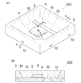
- (A) It is a schematic perspective view which shows the optical semiconductor device which concerns on other embodiment.
- (B) is an optical semiconductor device according to another embodiment, and is a schematic cross-sectional view showing a cross section taken along the line YY of FIG.
- FIG. 3 is a schematic cross-sectional manufacturing process diagram for explaining a manufacturing method of an optical semiconductor device.
- D is a schematic cross-sectional manufacturing process diagram for explaining a manufacturing method of an optical semiconductor device.
- Embodiment 1 Optical semiconductor device (No. 1) 1A and 1B show the structure of the optical semiconductor device 100 of the first embodiment.
- the optical semiconductor device 100 of the present embodiment is referred to as a lead frame 10 (hereinafter, also simply referred to as “lead frame 10”) composed of a light emitting element 2 which is rectangular in a plan view and a pair of plate-shaped metal structures 1 for an optical semiconductor device. ), And a resin molded body 3 in which a part of the lead frame 10 is embedded.
- the resin molded body 3 may be composed of a resin composition containing a thermoplastic resin or a thermosetting resin. Further, the resin molded body 3 can contain a filler such as TiO 2 as described later in the resin composition. This filler may be a reflective material that reflects the light from the light emitting element 2.
- the resin molded body 3 forms a recess having a bottom surface and a side surface, the bottom surface of the recess is composed of a part of a pair of lead frames 10, and the side surface is a side wall portion 31 as a reflective surface having a predetermined inclination angle. Is formed.
- the space between the pair of lead frames 10 is filled with the resin composition constituting the resin molded body 3, and constitutes a part 32 of the bottom surface of the resin molded body 3.
- the resin molded body 3 of the present embodiment has a horizontally long shape in a plan view. A part of a pair of plate-shaped lead frames 10 is exposed as an external terminal portion on the outer surface of the resin molded body 3, and the external terminal portion is bent along the lower surface of the resin molded body 3.
- the light emitting element 2 is mounted on one of the lead frames 10 that constitutes the bottom surface of the recess.
- the light emitting element 2 is covered with a sealing member 5.
- the sealing member 5 includes, for example, a phosphor that converts the wavelength of light from the light emitting element 2 and a sealing material.
- the material of the sealing member 5 preferably contains a translucent resin.
- the phosphor is excited by the light from the light emitting element 2 to wavelength-convert the light from the light emitting element 2 and emit light having at least one emission peak wavelength in a specific wavelength range.
- the light emitting element 2 has a pair of positive and negative electrodes, and the pair of positive and negative electrodes are electrically connected to the pair of lead frames 10 via wires 6, respectively.
- the optical semiconductor device 100 can emit light by receiving electric power from the outside via the pair of lead frames 10.
- the lead frame 10 or the substrate having a metal structure for an optical semiconductor device described in the embodiment described later has a portion that comes into contact with a member formed by using a resin material such as a resin molded body 3 or a sealing member 5. ..
- the package including the metal structure 1 for the optical semiconductor device and the resin molded body 3 constituting the lead frame 10 or the substrate constitutes the present embodiment, and the optical semiconductor device constituting the lead frame 10 or the substrate.
- the adhesion between the metal structure 1 for metal and the resin molded body 3 is improved.
- the metal structure 1 for an optical semiconductor device constituting the lead frame 10 or the substrate will be described in detail later.
- the resin material refers to a material containing at least a resin. Examples of the resin material include a resin composition containing a resin.
- the lead frame 10 made of the metal structure 1 for an optical semiconductor device serves as a mounting member for mounting the light emitting element 2, a reflecting member for reflecting light emitted from the light emitting element 2, and a conductive member electrically connected to the light emitting element 2. It also has the function of. Further, the lead frame 10 may also function as a heat radiating member that dissipates heat generated from the light emitting element 2.
- the lead frame 10 having a metal structure 1 for an optical semiconductor device may be provided below the light emitting element 2 as in the first embodiment, or may be provided in a reflector shape surrounding the light emitting element 2. Further, the lead frame 10 may be a plate-shaped lead frame.
- the metal structure 1 for an optical semiconductor device has the outermost layer 1d of gold, silver, a gold alloy or a silver alloy treated by dipping and / or applying a solution containing a polyallylamine polymer, it adheres to a resin.
- the properties are good, and in the optical semiconductor device 100, for example, the adhesion to the sealing member 5 and the resin molded body 3 can be improved.
- the method for forming the outermost layer 1d may be a known surface treatment and is not particularly limited. For example, plating (electrolytic plating, electroless plating, hot-dip plating, sputtering plating, vapor deposition plating including physical vapor deposition and chemical vapor deposition) ), Plating, etc. can be adopted.
- the content of a filler such as TiO 2 in the resin molded product is increased, or the color rendering property is improved.
- the content of the phosphor in the sealing member may be increased.
- the adhesion between the lead frame of the optical semiconductor device and the resin material tends to decrease.
- the lead frame 10 made of the metal structure 1 for the optical semiconductor device has high adhesion to the resin material, and therefore impurities (titanium oxide, phosphor, etc.) in the resin material.
- the metal structure 1 for an optical semiconductor device has the outermost layer 1d of gold, silver, gold alloy or silver alloy treated by dipping and / or coating a solution containing a polyallylamine polymer, silver or silver alloy. Even when the plating layer of No. 1 is provided as the outermost layer, discoloration due to sulfide or oxidation can be suppressed, a decrease in light beam due to sulfide discoloration or oxidative discoloration can be suppressed, and a high light beam can be maintained.
- Embodiment 2 Metal structure for optical semiconductor device (No. 1)
- the metal structure 1 for an optical semiconductor device can be used for a lead frame or a substrate. Further, by forming the metal structure 1 for an optical semiconductor device as wiring on an insulating substrate, it can be used for a printed circuit board, a ceramic substrate, or the like.
- the substrate is a member capable of comprising the metal structure 1 for an optical semiconductor device, and for example, a lead frame, a metal plate, a wire, a ceramic substrate, a printed circuit board, a flexible substrate, a silicon wafer, a GaAs wafer, and a GaN.
- It may be a ceramic component with a metal terminal such as a wafer or a capacitor, an organic component with a metal terminal such as a resistor, a pin connector, a round connector, a socket, a connector with a resin, or an airtight component such as a laser stem.
- a ceramic component with a metal terminal such as a wafer or a capacitor
- an organic component with a metal terminal such as a resistor, a pin connector, a round connector, a socket, a connector with a resin, or an airtight component such as a laser stem.
- FIG. 2A is a schematic cross-sectional view showing an embodiment of the metal structure 1 for an optical semiconductor device.
- the metal structure 1 for an optical semiconductor device is composed of a nickel or nickel alloy plating layer, a palladium or palladium alloy plating layer, a rhodium or rhodium alloy plating layer, and a platinum or platinum alloy plating layer between the outermost layer and the base material 1a. It can be equipped with at least one selected from the group.
- the metal structure 1 for an optical semiconductor device includes a conductive base material 1a containing, for example, copper or a copper alloy, and a conductive base material 1a containing, for example, copper or a copper alloy on a pair of two surfaces facing each other with the base material 1a as the center.
- a nickel or nickel alloy plating layer 1b and a surface layer 1d of a gold, silver, gold alloy or silver alloy treated by dipping and / or applying a solution containing a polyallylamine polymer on the base material 1a are arranged in this order. Can have.
- the metal structure 1 for an optical semiconductor device uses gold, silver, a gold alloy, or a silver alloy as the outermost layer.
- the Vickers hardness of gold and silver is smaller than the Vickers hardness of nickel, palladium, rhodium, and platinum, and since it is a soft metal, die bonding and wire bonding of the light emitting element 2 are facilitated.
- gold and silver are precious metals and are less likely to be oxidized than nickel, palladium, rhodium and platinum, and thus are less likely to affect solder mounting.
- the outermost surface layer of the metal structure 1 for an optical semiconductor device is a gold or gold alloy layer
- the outermost layer 1d is a silver or silver alloy layer
- a silver or silver alloy plating layer is formed as the outermost layer 1d
- gold or a gold alloy is plated as a base layer of the silver or silver alloy plating layer.
- layer 1c2 This is because gold is a more stable metal than silver. That is, when the outermost layer 1d is a silver or silver alloy layer, a gold or gold alloy plating layer 1c2 may be provided between the nickel or nickel alloy plating layer 1b and the outermost layer 1d.
- the pair of two opposing surfaces of the plate-shaped base material 1a may be referred to as the upper surface or the bottom surface, and the other two opposing surfaces of the plate-shaped base material 1a may be referred to as the side surfaces.
- the outermost surface layer 1d of gold, silver, a gold alloy, or a silver alloy does not have to be provided on all surfaces of the metal structure 1 for an optical semiconductor device. That is, at least a part of the surface of the metal structure 1 for an optical semiconductor device may be gold, silver, a gold alloy, or the outermost surface layer 1d of a silver alloy.
- the lead frame 10 not exposed on the bottom surface of the recess of the resin molded body 3 shown in FIG.
- the second embedded portion 13 in close contact with 5 is treated by dipping and / or applying a solution containing a polyallylamine polymer on its surface to treat gold, silver, gold alloy or It is preferable to have the outermost surface layer 1d of the silver alloy, but the external terminal portion exposed to the outside of the resin molded body 3 and the mounting portion exposed to the bottom surface side of the optical semiconductor device have gold, silver, gold alloy or gold, silver, or gold alloy on the surface thereof.
- the outermost surface layer 1d of the silver alloy may not be provided.
- the outermost layer 1d of gold, silver, gold alloy or silver alloy on a part of the metal structure 1 for an optical semiconductor device as described above, when forming the outermost layer 1d of gold, silver, gold alloy or silver alloy.
- the portion of gold, silver, gold alloy or silver alloy that does not require the outermost layer 1d is masked with a protective tape or the like, and the outermost layer 1d of gold, silver, gold alloy or silver alloy is formed on a part of the surface. Can be done.
- the outermost layer 1d of gold, silver, gold alloy or silver alloy treated by dipping and / or applying a solution containing a polyallylamine polymer is located at a site where it is not in direct contact with the resin molded body 3 or the sealing member 5. If there is, it may be provided on both of a pair of facing two surfaces of the plate-shaped metal structure 1 for an optical semiconductor device, for example, the upper surface and the bottom surface as in the present embodiment, and may be provided only on one surface and another. It does not have to be provided on the surface. Further, it may be provided only on a part of one surface.
- the outermost layer 1d of gold, silver, a gold alloy or a silver alloy treated by dipping and / or applying a solution containing a polyallylamine polymer may have the same thickness over the entire provided region. , The thickness may be different. By making the thickness different, the cost can be reduced more effectively.
- the outermost surface layer 1d of gold, silver, a gold alloy or a silver alloy treated by dipping and / or applying a solution containing a polyallylamine polymer is provided on the upper surface and the bottom surface of the metal structure 1 for an optical semiconductor device. The thickness on one side may be thicker than the other.
- the outermost layer 1d of gold, silver, gold alloy or silver alloy treated by dipping and / or applying a solution containing a polyallylamine polymer to a portion in direct contact with the resin molded body 3 or the sealing member 5 is provided.
- the metal structure 1 for an optical semiconductor device has a base material 1a having a surface layer 1d of gold, silver, a gold alloy, or a silver alloy treated by dipping and / or applying a solution containing a polyallylamine polymer.
- the base material 1a is used as a material for determining the rough shape of the metal structure 1 for an optical semiconductor device.
- the material of the base material 1a is not particularly limited, and copper, iron, alloys thereof, clad material (for example, copper / iron-nickel alloy / copper laminate) and the like can be preferably used.
- a copper alloy an alloy of copper and iron, tin, nickel, etc. can be adopted, and the copper content in that case is preferably 77.5% by mass or more and 99.5% by mass or less. ..
- an iron alloy an alloy of iron and nickel, cobalt or the like can be adopted, and the iron content in that case is preferably 55.0% by mass or more and 99.9% by mass or less. Copper and copper alloys are excellent in heat dissipation and can be preferably used.
- plate-shaped copper and copper alloys are preferable because they are excellent in terms of mechanical properties, electrical properties, workability, and the like. Since the clad material can suppress the coefficient of linear expansion to a low level, the reliability of the optical semiconductor device 100 can be improved.
- the thickness, shape, etc. of the base material 1a can be variously selected according to the shape, etc. of the optical semiconductor device 100. For example, it may have a plate-like shape, a lump-like shape, a film-like shape, or the like. Further, the wiring pattern may be provided on ceramic or the like by printing or the like, or the formed wiring pattern may be plated with copper or a copper alloy.
- the flatness of the base material 1a is preferably as high as possible.
- the surface roughness Ra of the base material 1a is preferably 0.5 ⁇ m or less.
- a nickel or nickel alloy plating layer 1b provided on the base material 1a as needed a palladium or palladium alloy plating layer provided as needed, a rhodium or rhodium alloy plating layer, a platinum or platinum alloy plating layer, etc.
- the flatness of the noble metal plating layer 1c1 made of the material and the outermost surface layer 1d of gold, silver, gold alloy or silver alloy can be further improved.
- the flatness of the base material 1a when the flatness of the base material 1a is high, the flatness of the outermost layer 1d of gold, silver, gold alloy or silver alloy having a thickness of 0.01 ⁇ m or more and 0.5 ⁇ m or less can be also high, and the optical semiconductor device can be increased.
- the reflectance of the metal structure 1 can be satisfactorily increased.
- the flatness of the base material 1a can be improved by performing treatments such as rolling, physical polishing, and chemical polishing, and by plating the same type of material as the material constituting the base material 1a, the base material 1a can be flattened.
- the flatness of 1a can also be increased. For example, in the case of the base material 1a made of a copper alloy, copper alloy plating can be performed to improve the flatness of the base material 1a.
- the metal structure 1 for an optical semiconductor device of the present embodiment preferably has a nickel or nickel alloy plating layer 1b on a base material 1a.
- the thickness of the nickel or nickel alloy plating layer 1b is preferably 0.5 ⁇ m or more and 10 ⁇ m or less, and more preferably 1 ⁇ m or more and 10 ⁇ m or less.
- the metal contained in the base material 1a to the base material 1a is a base layer of a palladium or palladium alloy plating layer, a rhodium or rhodium alloy plating layer, and platinum.
- the noble metal plating layer 1c1 composed of a platinum alloy plating layer or the like, or the outermost layer 1d of gold, silver, a gold alloy or a silver alloy.
- the thickness of the nickel or nickel alloy plating layer 1b is 10 ⁇ m or less, the raw material and the manufacturing cost can be reduced.
- the material of the nickel or nickel alloy plating layer 1b for example, in addition to nickel, alloys such as nickel phosphorus, nickel tin, and nickel cobalt can be used.
- the nickel content is preferably 90.0% by mass or more and 99.0% by mass or less.
- FIG. 2B is a schematic cross-sectional view showing another embodiment of the metal structure 1 for an optical semiconductor device.
- the metal structure 1 for an optical semiconductor device may have a base layer 1c between the nickel or nickel alloy plating layer 1b and the outermost layer 1d of gold, silver, gold alloy or silver alloy.
- the base layer 1c preferably has a noble metal plating layer 1c1 composed of a palladium or palladium alloy plating layer, a rhodium or rhodium alloy plating layer, a platinum or platinum alloy plating layer, or the like.
- the metal structure 1 for an optical semiconductor device has a pair of two surfaces facing each other with the base material 1a as the center, and on the base material 1a, for example, a nickel or nickel alloy plating layer 1b and a poly.
- the outermost layer 1d of gold, silver, gold alloy or silver alloy treated by dipping and / or coating a solution containing an allylamine polymer can be provided in this order.
- the metal structure 1 for an optical semiconductor device has a palladium or palladium alloy plating layer between the above-mentioned nickel or nickel alloy plating layer 1b and the outermost layer 1d of gold, silver, gold alloy or silver alloy.
- a noble metal plating layer 1c1 made of a rhodium or a rhodium alloy plating layer, a platinum or a platinum alloy plating layer or the like is provided. That is, the metal structure 1 for an optical semiconductor device is a noble metal plating composed of a base material 1a, a nickel or nickel alloy plating layer 1b, a palladium or palladium alloy plating layer, a rhodium or rhodium alloy plating layer, a platinum or platinum alloy plating layer, or the like.
- the layer 1c1 and the outermost layer 1d of gold, silver, a gold alloy, or a silver alloy treated by dipping and / or applying a solution containing a polyallylamine polymer are laminated in this order.
- the metal structure 1 for an optical semiconductor device has, for example, a nickel or nickel alloy plating layer 1b and, if necessary, so as to wrap around the base material 1a on two pairs of four surfaces facing each other with the plate-shaped base material 1a as the center.
- Silver, gold alloy, or the outermost surface layer 1d of the silver alloy may be provided in this order.
- the metal structure 1 for the optical semiconductor device is made of gold, silver, a gold alloy, or silver. It has an alloy as the outermost layer.
- the outermost surface layer of the metal structure 1 for an optical semiconductor device is a gold or gold alloy layer
- the outermost layer 1d is a silver or silver alloy layer
- a silver or silver alloy plating layer is formed as the outermost layer 1d
- gold or a gold alloy is plated as a base layer of the silver or silver alloy plating layer. It is preferable to form layer 1c2.
- the base layer 1c may be only the above-mentioned precious metal plating layer 1c1 or only the gold or gold alloy plating layer 1c2. Further, the gold or gold alloy plating layer 1c2 may be laminated on the noble metal plating layer 1c1, and the noble metal plating layer 1c1 and the gold or gold alloy plating layer 1c2 can be combined to form the base layer 1c.
- the metal structure 1 for an optical semiconductor device of the present embodiment comprises a palladium or palladium alloy plating layer, a rhodium or rhodium alloy plating layer, a platinum or platinum alloy plating layer, or the like as a base layer in contact with the nickel or nickel alloy plating layer 1b. It is preferable to have the noble metal plating layer 1c1.
- a nickel or nickel alloy plating layer 1b is provided on the base material 1a, and a palladium or palladium alloy plating layer, rhodium or rhodium alloy is provided as a second base layer on the base material 1a.
- a noble metal plating layer 1c1 composed of a plating layer, platinum or a platinum alloy plating layer, and further laminate gold, silver, the outermost layer 1d of a gold alloy or a silver alloy in this order.
- the copper contained in the base material 1a is further suppressed from diffusing into the outermost layer 1d of gold, silver, a gold alloy or a silver alloy. It is possible to improve the adhesion of each of the laminated layers. Further, since the diffusion of copper contained in the base material 1a is further suppressed, the wire bonding property can be further improved when the metal structure 1 for an optical semiconductor device is used as the lead frame 10.
- the thickness of the noble metal plating layer 1c1 is preferably 0.01 ⁇ m or more and 0.3 ⁇ m or less, more preferably 0.02 ⁇ m or more and 0.2 ⁇ m or less, and further preferably 0.03 ⁇ m or more and 0.1 ⁇ m or less.
- the metal contained in the base metal 1a diffuses to the outermost layer 1d of gold, silver, gold alloy or silver alloy. This can be further suppressed, and when the metal structure 1 for an optical semiconductor device is used as the lead frame 10, the wire bonding property can be further improved.
- the material of the palladium or palladium alloy plating layer for example, in addition to palladium, alloys such as nickel, phosphorus, cobalt, and copper can be used.
- the palladium content is preferably 75.0% by mass or more and 97.0% by mass or less.
- alloys such as nickel, cobalt, and platinum can be used.
- the rhodium content is preferably 75.0% by mass or more and 99.0% by mass or less.
- the material of the platinum or platinum alloy plating layer for example, in addition to platinum, alloys such as nickel, cobalt, and copper can be used.
- the platinum content is preferably 75.0% by mass or more and 99.0% by mass or less.
- the noble metal plating layer 1c1 which is the base layer of the outermost layer 1d of gold, silver, gold alloy or silver alloy serves as a layer having both a role of preventing sulfurization and preventing the diffusion of the metal contained in the base material 1a into other layers. May be good. Thereby, the cost can be further reduced. For example, gold does not easily react with the sulfur component and has a high effect of preventing the diffusion of the metal contained in the base material 1a, so that it can be preferably used.
- the metal structure 1 for an optical semiconductor device is preferably a substantially flat lead frame 10 as shown in FIGS. 3A and 3B described later, for example.
- the reliability of the metal structure 1 for an optical semiconductor device as a reflective member can be improved.
- the nickel or nickel alloy plating layer 1b is slightly more brittle than copper, iron, alloys thereof, clad material (for example, copper / iron nickel alloy / copper laminate) used as the base material 1a, the nickel or nickel alloy plating layer
- the metal structure 1 for an optical semiconductor device including 1b is preferably used as a flat plate without being bent.
- Embodiment 4 Optical semiconductor device (No. 2) 3A and 3B show the structure of the optical semiconductor device 200 of the fourth embodiment.
- the optical semiconductor device 200 of the present embodiment has a lead frame 10 having no bent portion.
- the members common to the optical semiconductor device 100 of the first embodiment are designated by the same reference numerals.
- Light emitting element 2 As the light emitting element 2, a semiconductor light emitting element having an arbitrary wavelength can be selected.
- a nitride semiconductor such as InGaN, GaN, or AlGaN, or one using GaP can be used.
- the red light emitting element GaAlAs, AlInGaP and the like can be used.
- a light emitting element 2 made of a material other than this can also be used. The composition, emission color, size, number, and the like of the light emitting element 2 to be used can be appropriately selected according to the purpose.
- the optical semiconductor device 100 or the optical semiconductor device 200 includes a member capable of wavelength conversion
- a nitride semiconductor capable of emitting a short wavelength capable of efficiently exciting the member capable of wavelength conversion is preferably mentioned.
- Various emission wavelengths can be selected depending on the material of the semiconductor layer and the mixed crystal ratio thereof.
- the light emitting element 2 can output not only light in the visible light region but also ultraviolet rays and infrared rays.
- the light emitting element 2 is preferably mounted on a lead frame 10 made of a metal structure 1 for an optical semiconductor device. Thereby, the light extraction efficiency of the optical semiconductor device 100 or the optical semiconductor device 200 can be further improved.
- the light emitting element 2 preferably has positive and negative electrodes that are electrically connected to the conductive member. These positive and negative electrodes may be provided on one surface side, or may be provided on both the upper and lower surfaces of the light emitting element 2.
- the connection with the conductive member may be made by the joining member 4 and the wire 6 described later, or by flip-chip mounting.
- the resin molded body 3 is a member made of a resin composition that integrally holds a pair of lead frames 10.
- the plan view shape of the resin molded body 3 may be a substantially rectangular shape in which a pair of opposite sides as shown in FIG. 1A is longer than the other facing sides, and a rectangular shape as shown in FIG. 3A. It may be.
- the resin molded body 3 may have a polygonal shape or a shape obtained by combining them.
- the side wall portion 31 of the recess may have an inclined surface whose inner side surface is provided at an inclined angle with respect to the bottom surface as shown in FIG. 3B, and has a substantially vertical angle.
- the lead frame 10 is provided inside the recess. It is preferable that the space between the pair of lead frames 10 and 10 is filled with the resin composition constituting the resin molded body 3 to form a part 32 of the bottom surface of the resin molded body 3.
- the resin molded body 3 can be formed by using a resin composition containing a thermosetting resin or a thermoplastic resin.
- a resin composition containing a thermosetting resin As the composition containing the thermosetting resin, a resin having a lower gas permeability than the resin used for the sealing member 5 is preferable, and specifically, an epoxy resin composition, a silicone resin composition, and a silicone-modified epoxy resin.
- modified epoxy resin compositions such as, modified silicone resin compositions such as epoxy modified silicone resins, polyimide resin compositions, modified polyimide resin compositions, urethane resins, modified urethane resin compositions and the like.
- the composition containing the thermoplastic resin a resin having low viscosity and easy flow is preferable, and specifically, polyamide, polyphthalamide (PPA), polycarbonate resin, polyphenylene terephide (PPS), liquid crystal polymer (LCP), and the like.
- examples thereof include acrylonitrile butadiene styrene copolymer resin (ABS resin), phenol resin, acrylic resin, polybutylene terephthalate resin (PBT resin) and the like.
- the resin composition constituting the resin molded body 3 includes TiO 2 , SiO 2 , Al 2 O 3 , MgO, MgCO 3 , CaCO 3 , Mg (OH) 2 , Ca (OH) 2, etc. as fillers.
- the inorganic particles as a filler in the resin composition constituting the resin molded body 3, the light transmittance of the resin molded body 3 can be adjusted.
- the amount of TiO 2 which is a white component in order to improve the reflectance of the resin material for the purpose of increasing the total light beam of the light emitting device for example, when the total amount of the resin composition is 100% by mass, the content of TiO 2 is contained.
- the amount is 20% by mass or more and 60% by mass or less
- the adhesion between the metal structure 1 for the optical semiconductor device and the resin material may be lowered.
- the member holding the lead frame 10 may be made of an inorganic substance such as ceramic, glass, or metal.
- the optical semiconductor device 100 or the optical semiconductor device 200 can be obtained with little deterioration and high reliability.
- the joining member 4 is a member for fixing and mounting the light emitting element 2 to the lead frame 10.
- the same material as the outermost layer 1d of copper, silver, gold particles, gold, silver, gold alloy or silver alloy can be used.
- an epoxy resin composition, a silicone resin composition, a polyimide resin composition, a modified resin thereof, a hybrid resin, or the like can be used.
- a metal layer having high reflectance such as an aluminum film or a silver film or a dielectric reflective film is provided on the mounting surface of the light emitting element 2 in consideration of deterioration due to light or heat from the light emitting element 2. be able to.
- the sealing member 5 is provided so as to cover each member of the light emitting element 2, the lead frame 10, the wire 6, and the protective film described later.
- the sealing member 5 By providing the sealing member 5 in the optical semiconductor device 100 or the optical semiconductor device 200, the coated member can be protected from dust, moisture, external force, and the like, and the reliability of the optical semiconductor device can be improved. ..
- the sealing member 5 on the protective film after forming the protective film the protective film can be protected, so that the reliability of the optical semiconductor device is enhanced.
- the sealing member 5 preferably has a light-transmitting property capable of transmitting light from the light emitting element 2 and a light resistance that is not easily deteriorated by them.
- Specific materials used for the sealing member 5 include a silicone resin composition, a modified silicone resin composition, a modified epoxy resin composition, a fluororesin composition, and the like, which have translucency capable of transmitting light from a light emitting element.
- An insulating resin composition can be mentioned.
- a hybrid resin containing at least one resin having a siloxane skeleton as a base such as dimethyl silicone, phenyl silicone having a low phenyl content, and a fluorine-based silicone resin, can also be used.
- the sealing member 5 is formed by using a potting (dropping) method, a compression molding method, a printing method, a transfer molding method, a jet dispensing method, a spray coating, or the like. be able to.
- the potting method is preferable, and when the optical semiconductor device uses a flat plate-shaped substrate, the compression molding method or the transfer molding method is preferable.
- the sealing member 5 is preferably provided so as to fill the recessed portion of the resin molded body 3.
- the shape of the outer surface of the sealing member 5 can be variously selected according to the light distribution characteristics required for the optical semiconductor device 100 and the like. For example, by making the upper surface a convex lens shape, a concave lens shape, a Fresnel lens shape, a rough surface, or the like, the directivity characteristics and the light extraction efficiency of the optical semiconductor device can be adjusted.
- the sealing member 5 can also contain a colorant, a light diffusing material, a light reflecting material, various fillers, a wavelength conversion member, and the like.
- the wavelength conversion member is a material that converts the light of the light emitting element 2 into wavelength.
- the yttrium aluminum garnet phosphor (hereinafter referred to as "YAG: Ce”), which is a kind of aluminum oxide phosphor, is preferable as the wavelength conversion member. Used for. Since the YAG: Ce phosphor absorbs a part of the blue light from the light emitting element and emits the yellow light as a complementary color, it is relatively easy to use a high-output optical semiconductor device that emits a white mixed color light. Can be formed into.
- the wire 6 connects the light emitting element 2 and a conductive member such as the lead frame 10.
- a conductive member such as the lead frame 10.
- gold, silver, aluminum, copper, alloys thereof and the like are preferably used.
- a wire 6 having a coating layer provided on the surface of the core with a material different from that of the core for example, a wire 6 provided with a coating layer of palladium, palladium gold alloy or the like on the surface of the copper core can also be used.
- the material of the wire 6 is preferably selected from any one of highly reliable gold, silver, and silver alloy. Further, in particular, silver or a silver alloy having a high light reflectance is preferable.
- the wire 6 is covered with a protective film. This makes it possible to further prevent sulphurization and disconnection of the wire containing silver, and further enhance the reliability of the optical semiconductor device 100.
- the base material 1a of the metal structure for the optical semiconductor device constituting the lead frame 10 contains copper and the wire 6 is made of silver or a silver alloy
- the metal structure 1 for the optical semiconductor device is a nickel or nickel alloy plating layer. By providing 1b, the formation of a local battery between copper and silver can be suppressed. As a result, deterioration of the lead frame 10 and the wire 6 is further suppressed, and a more reliable optical semiconductor device can be obtained.
- the wire 6 may include the metal structure 1 for an optical semiconductor device, similarly to the lead frame 10 having the metal structure 1 for an optical semiconductor device described above.
- the wire 6 since it has the outermost layer 1d obtained by dipping and / or applying a solution containing a polyallylamine polymer, it has good adhesion to a resin, and in the optical semiconductor device 100 or the optical semiconductor device 200, for example, it is sealed. The adhesion with the stop member 5 can be improved.
- the optical semiconductor device 100 or the optical semiconductor device 200 may further include a protective film.
- the protective film can cover at least the outermost layer 1d of gold, silver, a gold alloy, or a silver alloy provided on the surface of the metal structure 1 for an optical semiconductor device constituting the lead frame 10.
- the protective film is a member that suppresses discoloration or corrosion of the outermost layer 1d of gold, silver, a gold alloy, or a silver alloy on the surface of the metal structure 1 for an optical semiconductor device that mainly constitutes the lead frame 10.
- the protective film is optionally provided with the surface of a member other than the lead frame 10 or the substrate such as the light emitting element 2, the joining member 4, and the resin molded body 3, and the outermost layer 1d of gold, silver, gold alloy, or silver alloy.
- the surface of the metal structure 1 for an optical semiconductor device which has not been provided may be coated.
- the protective film is provided so as to cover the wire 6 or the outermost layer 1d. Is preferable. This makes it possible to further prevent sulphurization and disconnection of the wire containing silver, and further enhance the reliability of the optical semiconductor device 100 or the optical semiconductor device 200.
- the protective film is preferably formed by a sputtering method, a chemical vapor deposition method, or an atomic layer deposition method (hereinafter, also referred to as ALD (Atomic Layer Deposition)).
- ALD atomic layer deposition
- a very uniform protective film can be formed, and the formed protective film is denser than the protective film obtained by other film forming methods. Therefore, for example, a lead. It is possible to very effectively prevent sulfide and discoloration of the outermost layer 1d of the metal structure 1 for an optical semiconductor device constituting the frame 10.
- Materials for the protective film include Al 2 O 3 , SiO 2 , TiO 2 , ZrO 2 , ZnO, Nb 2 O 5 , MgO, In 2 O 3 , Ta 2 O 5 , HfO 2 , SeO, Y 2 O 3 , Examples thereof include oxides such as SnO 2 , nitrides such as AlN, TiN and ZrN, and fluorides such as ZnF 2 and SrF 2. These may be used alone or in combination. Alternatively, they may be laminated.
- the optical semiconductor device 100 or the optical semiconductor device 200 can be provided with various members in addition to the above.
- a Zener diode can be mounted as a protection element.
- a lead frame 10 having a metal structure 1 for an optical semiconductor device according to a second or third embodiment is prepared. Specifically, for example, a copper metal plate constituting the base material 1a of the metal structure 1 for an optical semiconductor device is punched, and as described later in the method for manufacturing the metal structure 1 for an optical semiconductor device, if necessary.
- a noble metal plating layer 1c1 composed of nickel or nickel alloy plating layer 1b, palladium or palladium alloy plating layer, rhodium or rhodium alloy plating layer, platinum or platinum alloy plating layer, etc., and gold, silver, gold alloy or silver alloy, if necessary.
- a lead frame which is a lead frame formed by forming the outermost layer 1d of the above, dipping and / or applying it in a solution containing a polyallylamine polymer, and then washing with water or hot water (washing) as necessary and drying.
- the resin molded body 3 can be molded by the transfer molding method so as to be in contact with the lead frame 10 using the metal structure 1 for an optical semiconductor device.
- the resin molded body 3 may be formed so that the pair of lead frames 10 are each exposed on the bottom surface of the recess of the resin molded body 3. That is, the lead frame 10 can be exposed on the bottom surface of the recess of each resin molded body 3.
- the light emitting element 2 can be mounted via the joining member 4 in the region where the light emitting element 2 of the lead frame 10 on which the resin molded body 3 is formed is mounted. Then, the light emitting element 2 and the lead frame 10 can be connected by a wire. After that, the sealing member 5 can be provided in each recess of the resin molded body 3.
- the lead frame 10 and the resin molded body 3 as shown in FIG. 4D can be cut with a dicing saw or the like and separated into individual optical semiconductor devices as shown in FIGS. 3A and 3B.
- the cross section of the lead frame 10 is exposed on the outer surface of the optical semiconductor device 200.
- a base material 1a such as copper of the metal structure 1 for an optical semiconductor device constituting the lead frame 10, a nickel or nickel alloy plating layer 1b if necessary, and a palladium or palladium alloy plating layer if necessary.
- a noble metal plating layer 1c1 composed of a rhodium or rhodium alloy plating layer, a platinum or platinum alloy plating layer, and the outermost layer of a treated gold, silver, gold alloy, or silver alloy that has been immersed and / or coated in a solution containing a polyallylamine polymer. 1d is exposed.
- Embodiment 5 Method for manufacturing metal structure for optical semiconductor device Next, a method for manufacturing a metal structure for optical semiconductor device will be described.
- the method for manufacturing a metal structure for an optical semiconductor device is as follows. (1) At least one selected from the group consisting of gold, silver, gold alloys and silver alloys (preferably at least one selected from the group consisting of gold, silver, gold alloys and silver alloys) in part or on the entire surface.
- a treatment step of dipping and / or applying a solution containing a polyallylamine polymer to a substrate having an outermost layer (gold, silver, gold alloy or outermost surface layer 1d of a silver alloy) having (plating) is provided.
- the plating is a metal film formed by, for example, wet plating such as electrolytic plating and electroless plating, and dry plating such as hot-dip plating, sputtering plating, and vapor deposition plating including physical vapor deposition and chemical vapor deposition.
- the substrate may include an outermost layer having at least one selected from the group consisting of gold, silver, gold alloys and silver alloys, and the outermost layer does not have to be a metal film formed by surface treatment. ..
- the substrate itself may be at least one selected from the group consisting of gold, silver, gold alloys and silver alloys.
- the substrate can also be subjected to the above step after forming a step at a predetermined position by wet etching and forming the step.
- a nickel or nickel alloy plating layer 1b if necessary, a palladium or palladium alloy plating layer, a rhodium or rhodium alloy plating layer, platinum or platinum alloy plating. It is preferable to form the noble metal plating layer 1c1 composed of layers and the like. Therefore, before performing the above-mentioned step (1), a step of forming a nickel or nickel alloy plating layer 1b on the base material 1a as needed, and a step of forming the nickel or nickel alloy plating layer 1b on the nickel or nickel alloy plating layer 1b as needed.
- the steps of forming the outermost layer 1d of gold, silver, gold alloy or silver alloy are the step of forming the plating layer of gold or gold alloy and silver.
- the thickness of the gold or gold alloy plating layer 1c2 can be 0.003 ⁇ m or more and 0.5 ⁇ m or less.
- the outermost layer 1d is not necessarily limited to plating, and may be a metal film formed by thermal spraying.
- the step of forming each of these layers is easy, it is preferable to carry out by the method of forming a metal film by the above-mentioned plating, and more preferably by electrolytic plating or electroless plating. Among them, electrolytic plating is preferable because the layer formation speed is high and mass productivity can be improved.
- the base material 1a Before forming each of the above layers, the base material 1a can be pretreated.
- the pretreatment include acid treatment of dilute sulfuric acid, dilute nitric acid, dilute hydrochloric acid and the like, alkali treatment of sodium hydroxide and the like, and these may be performed once or several times with the same treatment or a combination of different treatments. .. When the pretreatment is performed several times, it is preferable to wash with running water using pure water after each treatment.
- the base material 1a is a metal plate made of copper or a copper alloy, it is preferable to use dilute sulfuric acid for the pretreatment.
- the base material 1a is a metal plate made of iron or an iron alloy, it is preferable to use dilute hydrochloric acid for the pretreatment.
- the nickel or nickel alloy plating layer 1b when the material constituting the plating layer is pure nickel, it can be formed by electrolytic plating using, for example, a plating solution containing nickel sulfamate. When a nickel-phosphorus alloy is used, it can be formed by electroless plating using a nickel hypophosphate plating solution.
- the noble metal plating layer 1c1 composed of palladium or palladium alloy plating layer, rhodium or rhodium alloy plating layer, platinum or platinum alloy plating layer, etc.
- the material constituting the plating layer is palladium or palladium alloy, for example. It can be formed by electrolytic plating using a plating solution containing tetraammine-palladium chloride.
- the material constituting the plating layer is rhodium or a rhodium alloy, it can be formed by electrolytic plating using, for example, a plating solution containing rhodium sulfate.
- the material constituting the plating layer is platinum or a platinum alloy, it can be formed by electrolytic plating using, for example, a plating solution containing a dinitrodiamine platinum salt.
- the outermost surface layer 1d of gold, silver, a gold alloy, or a silver alloy is provided on the surface of the metal structure 1 for an optical semiconductor device.
- the thickness of the outermost surface layer 1d of gold, silver, a gold alloy or a silver alloy is 0.003 ⁇ m or more and 0.5 ⁇ m or less, preferably 0.01 ⁇ m or more and 0.3 ⁇ m or less.
- the die bonding property with the light emitting element 2 and the wire bonding property with the wire 6 can be further improved.
- the thickness of the outermost surface layer 1d of gold, silver, a gold alloy or a silver alloy is 0.5 ⁇ m or less, the amount of expensive precious metal used can be further reduced, and the cost can be further reduced.
- the gold content is preferably 75.0% by mass or more and 99.9% by mass or less, and when a silver alloy is used, the silver content is 75.0% by mass. It is preferably% or more and 99.9% by mass or less.
- the outermost surface layer 1d is a gold or gold alloy layer
- potassium gold cyanide or gold cyanide is added at a metal gold concentration of 0.5 g / L or more and 10 g / L. It is preferable to use a plating solution containing L or less and containing 30 g / L or more and 150 g / L or less of an electrically conductive salt.
- a gold-silver alloy plating or a gold-copper alloy plating layer can be obtained by adding silver potassium cyanide, potassium copper cyanide, or the like as an alloy metal in an amount of 1 g / L or more and 5 g / L or less, respectively.
- the outermost surface layer 1d is a silver or silver alloy layer, and when the silver or silver alloy layer is formed by electrolytic plating, it contains 20 g / L or more and 80 g / L or less of silver potassium cyanide or silver cyanide as metallic silver. It is preferable to use a plating solution containing 50 g / L or more and 150 g / L or less of free potassium cyanide or an electrically conductive salt. Further, a selenium compound or an organic sulfur compound can be further added to this plating solution as a brightener.
- silver alloy plating it is possible to obtain a silver-gold alloy plating or a silver-copper alloy plating layer by adding 5 g / L or more and 20 g / L or less of potassium gold cyanide or potassium copper cyanide as an alloy metal, respectively. it can.
- the plating solution preferably contains 5 g / L or more and 150 g / L or less of one or more kinds of electrically conductive salts such as cyanate, carbonate, phosphate, nitrate, citrate, and sulfate.
- electrically conductive salts such as cyanate, carbonate, phosphate, nitrate, citrate, and sulfate.
- the electric conductive salt contained in the plating solution is 5 g / L or more and 150 g / L or less, the viscosity of the plating solution does not become excessive, and the so-called carry-out of the plating solution by the object to be plated is reduced. It can be economically plated with gold, silver, gold alloys or silver alloys.
- the cyanide salt include potassium cyanide and sodium cyanide.
- the carbonate include potassium carbonate, sodium carbonate, ammonium carbonate and the like.
- the phosphate include potassium phosphate, sodium phosphate, ammonium phosphate, potassium pyrophosphate and the like.
- Examples of the nitrate include potassium nitrate, sodium nitrate, ammonium nitrate and the like.
- Examples of the citrate include potassium citrate, sodium citrate, ammonium citrate and the like.
- Examples of the sulfate include potassium sulfate, sodium sulfate and the like.
- the temperature of the plating solution is 20 ° C. or higher and 70 ° C. or lower, and the electrode is made of gold, silver or gold-silver alloy. becomes soluble electrode or, stainless steel or platinum, using a platinum-coated titanium electrode, a cathode current density of the conductive substrate is a 0.1 a / dm 2 or more 10A / dm 2 or less, 10 minutes plating time is 5 seconds or more It is preferable to perform electrolytic plating under the following conditions.
- the gold, silver, gold alloy or silver alloy layer which is the outermost surface layer 1d is not a metal film formed by plating, spraying or the like, for example, a metal plate or a wire, it is formed or prepared by a conventional method. be able to.
- the outermost layer 1d of gold, silver, a gold alloy or a silver alloy is treated by dipping and / or applying a solution containing a polyallylamine polymer.
- the film containing the polyallylamine polymer adheres to the substrate including the outermost layer 1d of gold, silver, a gold alloy or a silver alloy.
- the thickness of the film containing the polyallylamine polymer is preferably 10 nm or more and 500 nm or less. By setting the thickness of the film containing the polyallylamine polymer to 500 nm or less, die bonding, wire bonding, or solder mounting of the light emitting device can be further improved. Further, by setting the thickness of the film containing the polyallylamine polymer to 10 nm or more, the adhesion between the metal structure 1 for an optical semiconductor device and the resin material can be further improved.
- the polyallylamine polymer is not particularly limited, but usually, a homopolymer of allylamine, which is a primary amine, is assumed, and specifically, it is assumed.
- n 25 to 440.
- examples thereof include a polyallylamine polymer represented by. These polyallylamine polymers can be used alone or in combination of two or more.
- the weight average molecular weight of the polyallylamine polymer described above is preferably 1600 or more and 25,000 or less, and more preferably 3000 or more and 18,000 or less, from the viewpoint of adhesion to the resin material.
- polyallylamine polymer As the polyallylamine polymer as described above, a known or commercially available product can be used, or a polymer can be used. When a commercially available product is used, it can be easily obtained because it is sold by Nittobo Medical Co., Ltd. under the trade name PAA (registered trademark).
- this polyallylamine polymer is water-soluble, aqueous solutions of various concentrations can be produced.
- the total amount of the solution containing the polyallylamine polymer is 100% by mass, and the aqueous solution is preferably 0.01% by mass or more and 1.0% by mass or less. It is more preferable to use an aqueous solution of 05% by mass or more and 0.5% by mass or less.
- the concentration of the solution containing the polyallylamine polymer By setting the concentration of the solution containing the polyallylamine polymer to 1.0% by mass or less, not only the adhesion to the resin material is improved, but also the viscosity of the aqueous solution is not made too high, and the metal structure for optical semiconductor devices is used. It is more economical because the treatment liquid is less likely to be taken out together with 1.
- the solution containing the polyallylamine polymer may contain a triazine compound. That is, the membrane containing the polyallylamine polymer adhering to the substrate may contain a triazine compound.
- the adhesion to the resin material can be further improved. Since the triazine compound has excellent adhesion to gold, the adhesion to the resin material can be particularly improved when a gold or gold alloy layer is used as the outermost layer 1d.
- a triazine thiol compound is preferable from the viewpoint of easily improving the adhesion with the resin material.
- Y represents a nitrogen atom or a sulfur atom.
- R 1 , R 2 and R 3 are the same or different and represent a hydrogen atom, an alkali metal atom or a substituted or unsubstituted alkyl group.
- m indicates 1 or 2
- m indicates 2 when Y is a nitrogen atom
- m indicates 1 when Y is a sulfur atom.
- Examples thereof include triazine compounds represented by.
- examples of the alkali metal atom represented by R 1 , R 2 and R 3 include a lithium atom, a sodium atom, a potassium atom, a cesium atom and the like.
- the alkyl groups represented by R 1 , R 2 and R 3 include methyl group, ethyl group, n-propyl group, isopropyl group, n-butyl group, isobutyl group and sec-butyl group. Examples thereof include alkyl groups having 1 to 10 carbon atoms (particularly 1 to 6) such as tert-butyl groups. These alkyl groups may have 1 to 3 substituents such as a halogen atom (chlorine atom, bromine atom, iodine atom, etc.).
- triazine compounds may be used alone or in combination of two or more.
- triazine compounds known or commercially available products can be used.
- the sodium salt of 1,3,5-triazine-2,4,6-thiol is sold by Sankyo Kasei Co., Ltd. under the trade name of Santhiol, and is easily available and water-soluble. Therefore, it is preferable because a treatment liquid having an appropriate concentration can be prepared.
- the above-mentioned triazine compound is composed of 100% by mass of the total amount of the solution containing the polyallylamine polymer.
- the content is preferably 0.01% by mass or more and 1.0% by mass or less, and more preferably 0.05% by mass or more and 0.5% by mass or less.
- the concentration of the solution containing the triazine compound By setting the concentration of the solution containing the triazine compound to 1.0% by mass or less, not only the adhesion to the resin material is improved, but also the viscosity of the aqueous solution is not made too high, together with the metal structure 1 for an optical semiconductor device. It is more economical because the treatment liquid is less likely to be taken out.
- Triazine compounds have excellent adhesion to gold and silver (especially gold), and triazine thiol compounds have good adhesion to gold due to the intermolecular force between gold and S (sulfur), but their effectiveness is effective when washed with water. There is a concern that it will weaken.
- the polyallylamine polymer has a large molecular weight, and the solution containing the polyallylamine polymer is sticky. Therefore, the polyallylamine polymer adheres to the surface of the outermost layer 1d of gold, silver, a gold alloy, or a silver alloy by the treatment of the present embodiment. It is easy to form a film containing an allylamine polymer.
- the film containing the polyallylamine polymer improves the adhesion between the outermost layer 1d of gold, silver, a gold alloy or a silver alloy and the resin material, and when the film containing the polyallylamine polymer contains a triazine compound. Since the film containing the polyallylamine polymer retains the triazine compound, it is presumed that a better effect can be obtained in improving the adhesion.
- an appropriate anionic surfactant and cationic surfactant are used in order to further improve the wettability and dissolution stability of gold, silver, a gold alloy or a silver alloy to the outermost layer 1d.
- Activators, nonionic surfactants and the like can also be added.
- an appropriate organic solvent or an appropriate pH buffer can be added.
- the pH buffer include boric acid or a salt thereof, diphosphate or a salt thereof, phosphoric acid or a salt thereof, or citric acid or a salt thereof.
- a concentrated solution may be prepared in advance, and when used in a processing apparatus, this concentrated solution may be appropriately diluted with water before use.
- the above-mentioned solution containing the polyallylamine polymer is particularly useful for being used for improving the adhesion between the lead frame 10 in the optical semiconductor device 100 or the optical semiconductor device 200 and the adjacent resin molded product 3. is there.
- a method for treating a solution containing a polyallylamine polymer with respect to gold, silver, a gold alloy or a silver alloy layer it is preferable to perform treatment by dipping and / or coating.
- the gold, silver, gold alloy or silver alloy layer may be all immersed in the solution containing the polyallylamine polymer, or only the portion in contact with the resin material may be immersed.
- the coating treatment particularly the spraying treatment
- the solution containing the polyallylamine polymer may be coated by a known means, or the spraying treatment (spraying treatment or the like) may be performed by a known means.
- the gold, silver, gold alloy or silver alloy layer may be sprayed at a right angle, or may be sprayed horizontally or at an angle. Further, it may be a spray jet or a shower. Further, both the dipping and the coating may be performed, and the order thereof is not particularly limited.
- the temperature of the solution containing the polyallylamine polymer is preferably 15 ° C. or higher and 50 ° C. or lower.
- the temperature of the solution is preferably 15 ° C. or higher and 50 ° C. or lower.
- the time for dipping and / or coating the solution containing the polyallylamine polymer on the gold, silver, gold alloy or silver alloy layer can be appropriately adjusted depending on the dipping and / or coating method and the temperature of the treatment liquid, but it is usually used. It is preferably 3 seconds or more and 60 seconds or less. By setting the treatment time to 3 seconds or more, it is easy to more uniformly adhere the film of the polyallylamine polymer and, if necessary, the triazine compound to the surface of the gold, silver, gold alloy or silver alloy layer. Further, by setting the processing time to 60 seconds or less, the productivity can be further improved.
- step (1) In the manufacturing method of the present embodiment, after the step (1) is performed in this way, (2) A step of cleaning the substrate that has undergone the step (1) and (3) a step of drying the substrate that has undergone the step (2) can be provided in this order. Washing (particularly water washing or hot water washing) and drying can be performed according to a conventional method.
- the metal structure 1 for an optical semiconductor device may further include a step of heat treatment as step (4) after forming each layer.
- a step (4) of heat-treating the substrate that has undergone the step (2) may be provided.
- the heat treatment may be performed in the atmosphere, an inert atmosphere such as nitrogen gas, or a reducing atmosphere such as hydrogen gas.
- a batch process such as in a hot air incubator may be used, or a hot air furnace or an infrared furnace may be provided in the final step of the continuous plating apparatus for continuous heat treatment.
- the base material 1a and the metals of each layer are appropriately diffused with each other, and the adhesion between the base material 1a and the nickel or nickel alloy plating layer 1b and between the base materials 1b, 1c and 1d is likely to be improved.
- the heat treatment temperature and the treatment time can be determined in consideration of the combination of the thicknesses of each layer, but the heat treatment temperature is usually preferably 100 ° C. or higher and 500 ° C. or lower.
- a nickel plating layer, a nickel tin alloy plating layer or a nickel cobalt alloy plating layer is plated on the surface of the following base material 1a as the nickel or nickel alloy plating layer 1b, and gold plating is performed on the surface of the base material 1a as the outermost layer 1d.
- a metal structure 1 for an optical semiconductor device was formed by electrolytic plating on the layers in this order using each plating solution having the bath composition shown below.
- a step of dipping or spraying in a solution containing a polyallylamine polymer, a step of washing, and a step of drying are performed, and the lead frame 10 which is a pair of lead frames is used by using the metal structure 1 for an optical semiconductor device.
- the thickness ( ⁇ m) of each layer in the examples, the composition of the solution containing the polyallylamine polymer, and the treatment conditions are shown in Table 1.
- Copper base material TAMAC194 material manufactured by Mitsubishi Shindoh Co., Ltd. was used in a lead frame shape with a press die.
- Iron base material SPCE-SB manufactured by Nippon Steel Corporation was used with a press die in the shape of a lead frame.
- Nickel or nickel alloy plating layer 1b of Examples 1, 4, 5, 7 and 11 As the nickel or nickel alloy plating layer 1b, the nickel plating layer was formed in Examples 1, 4 and 11, the nickel tin alloy plating layer was formed in Example 5, and the nickel cobalt alloy plating layer was formed in Example 7.
- a plating solution having the following bath composition was used as a standard sulfamic acid electrolytic plating bath.
- the nickel tin alloy plating layer As the nickel tin alloy plating layer, a plating solution in which an appropriate amount of tin sulfamate (5 g / L) was added to the above nickel plating layer was used.
- nickel-cobalt alloy plating layer As the nickel-cobalt alloy plating layer, a plating solution in which an appropriate amount of cobalt sulfamate (15 g / L) was added to the above-mentioned nickel plating layer was used.
- the plating time was adjusted and electrolytic plating was performed at a liquid temperature of 55 ° C. and a cathode current density of 5 A / dm 2 to form a nickel plating layer, a nickel tin alloy plating layer or a nickel cobalt alloy plating layer.
- a sulfur-added nickel plate was used as the anode.
- the plating time was adjusted using the plating solution, and electrolytic plating was performed at a solution temperature of 68 ° C. and a cathode current density of 0.5 A / dm 2 to form a gold plating layer.
- a platinum-coated titanium-insoluble electrode was used as the anode.
- Example 5 the polyallylamine polymer PAA-08 (registered trademark; weight average molecular weight 8000) manufactured by Nittobo Medical Co., Ltd. was 0.02% by mass and 1,3,5-triazine-2,4,6- An aqueous solution containing 0.2% by mass of thioltrisodium salt (Santhiol NW manufactured by Sankyo Kasei Co., Ltd.) was sprayed at 50 ° C. for 35 seconds, washed with water and dried.
- thioltrisodium salt Santhiol NW manufactured by Sankyo Kasei Co., Ltd.
- Example 11 the polyallylamine polymer PAA-15 (registered trademark; weight average molecular weight 15000) manufactured by Nittobo Medical Co., Ltd. was added in an amount of 0.01% by mass and 1,3,5-triazine-2,4,6- It was immersed in an aqueous solution containing 0.1% by mass of thioltrisodium salt (Santhiol NW manufactured by Sankyo Kasei Co., Ltd.) at 15 ° C. for 3 seconds, washed with water and dried.
- thioltrisodium salt Santhiol NW manufactured by Sankyo Kasei Co., Ltd.
- a nickel plating layer or a nickel phosphorus alloy plating layer is used as a nickel or nickel alloy plating layer 1b, and a palladium plating layer or a palladium nickel alloy plating is used as a base layer 1c on the nickel plating layer or a nickel phosphorus alloy plating layer.
- a layer, a rhodium plating layer or a rhodium cobalt alloy plating layer is placed on top of the gold plating layer, a gold-silver alloy plating layer or a gold cobalt plating layer as the outermost layer 1d, and each plating solution having the bath composition shown below is applied in this order.
- the metal structure 1 for an optical semiconductor device was formed by electrolytic plating under each condition. After that, a treatment step of immersing in a solution containing a polyallylamine polymer, a washing step, a drying step, and a heat treatment step if necessary are performed, and a pair of metal structures 1 for an optical semiconductor device are used.
- a lead frame 10 which is a lead frame was prepared. The thickness of each layer in the examples, the composition of the solution containing the polyallylamine polymer, and the treatment conditions are shown in Table 1.
- Nickel or nickel alloy plating layer 1b of Examples 2, 3, 6, 8, 9 and 10 As the nickel or nickel alloy plating layer 1b, the nickel plating layer was formed in Examples 2, 3, 6, 8 and 10, and the nickel phosphorus alloy plating layer was formed in Example 9.
- the nickel plating layers of Examples 2, 3, 6, 8 and 10 used the same plating solution as in Example 1 except that the plating thickness was set to the one shown in Table 1.
- the nickel-phosphorus alloy plating layer As the nickel-phosphorus alloy plating layer, a plating solution in which an appropriate amount of phosphorous acid (20 g / L) was added to the above nickel-plated layer was used.
- the plating time was adjusted and electrolytic plating was performed at a liquid temperature of 55 ° C. and a cathode current density of 5 A / dm 2 to form a nickel plating layer or a nickel phosphorus alloy plating layer.
- a sulfur-added nickel plate was used as the anode.
- Base layer 1c of Examples 2, 3, 6, 8, 9 and 10 As the base layer 1c, a palladium plating layer is formed in Examples 2, 9 and 10, a rhodium plating layer is formed in Example 3, a palladium nickel alloy plating layer is formed in Example 6, and rhodium cobalt is formed in Example 8. An alloy plating layer was formed.
- a plating solution having the following bath composition was used as the palladium plating layer.
- Sodium 3-pyridinesulfonate 5 g / L pH 8.5.
- Example 6 For the palladium-nickel alloy plating layer of Example 6, a plating solution obtained by adding an appropriate amount of nickel sulfate (1.0 g / L) to the above-mentioned palladium plating solution was used.
- the plating time was adjusted using the plating solution, and electrolytic plating was performed at a solution temperature of 50 ° C. and a cathode current density of 1 A / dm 2 to form a palladium plating layer or a palladium nickel alloy plating layer.
- a platinum-coated titanium electrode was used as the anode.
- a plating solution having the following bath composition was used as the rhodium plating layer as the base layer 1c of Example 3.
- a plating solution obtained by adding an appropriate amount of cobalt sulfate (0.3 g / L) to the rhodium plating solution was used.
- the plating time was adjusted using the plating solution, and electrolytic plating was performed at a solution temperature of 45 ° C. and a cathode current density of 1 A / dm 2 to form a rhodium plating layer.
- a platinum-coated titanium electrode was used as the anode.
- Example 2 For the gold-silver alloy plating layer 1d of Example 2, a plating solution having the following bath composition was used.
- the plating time was adjusted and electrolytic plating was performed at a liquid temperature of 30 ° C. and a cathode current density of 1 A / dm 2 to form a gold-silver alloy plating layer.
- a platinum-coated titanium electrode was used as the anode.
- the plating time was adjusted using the same plating solution as in Example 1 except that the gold plating layer had the plating thickness shown in Table 1 as the outermost surface layer 1d of Examples 3, 6, 8 and 10. However, the gold plating layer was formed under the same conditions as in Example 1 except for the above.
- the plating time was adjusted by using a plating solution obtained by adding an appropriate amount of cobalt sulfate (1.0 g / L) to the gold plating solution of Example 1.
- the gold-cobalt alloy plating layer was formed under the same conditions as in Example 1 except for the above.
- the polyallylamine polymer PAA-08 (registered trademark; weight average molecular weight 8000) manufactured by Nittobo Medical Co., Ltd. was added in an amount of 0.02% by mass and 1,3,5-triazine-2,4. It was immersed in an aqueous solution containing 0.2% by mass of 6-thioltrisodium salt (Santhiol NW manufactured by Sankyo Kasei Co., Ltd.), washed with water and dried. The immersion conditions are shown in Table 1.
- Example 3 0.01% by mass of the polyallylamine polymer PAA-15 (registered trademark; weight average molecular weight 15000) manufactured by Nittobo Medical Co., Ltd. and 1,3,5-triazine-2, It was immersed in an aqueous solution containing 0.1% by mass of 4,6-thioltrisodium salt (Santhiol NW manufactured by Sankyo Kasei Co., Ltd.), washed with water and dried, and in Example 9, the temperature was further increased to 250 ° C. Heat-treated for 2 hours. The immersion conditions are shown in Table 1.
- Example 10 the polyallylamine polymer PAA-03 (registered trademark; weight average molecular weight 3000) manufactured by Nittobo Medical Co., Ltd. was immersed in an aqueous solution containing 0.5% by mass at 20 ° C. for 20 seconds, and after washing with water. It was dried and further heat treated at 450 ° C. for 5 minutes.
- the immersion conditions are shown in Table 1.
- Comparative Examples 1, 2 and 3 As Comparative Example 1, a metal structure having the same structure as that of Example 1 and having the thicknesses of the nickel plating layer and the gold plating layer shown in Table 1 was prepared, but was not treated with a solution containing a polyallylamine polymer. .. As Comparative Examples 2 and 3, a metal structure having the same structure as in Example 10 and having the thicknesses of the nickel plating layer, the palladium plating layer, and the gold plating layer at the ratio shown in Table 1 was prepared, but the polyallylamine weight was prepared. It was not treated with a solution containing coalescence. A lead frame 10 which is a pair of lead frames was prepared using this metal structure.
- each optical semiconductor device having substantially the same structure as the optical semiconductor devices shown in FIGS. 1A and 1B was manufactured. Until the optical semiconductor device 100 is fragmented, each step is performed in the state of an aggregate in which a plurality of resin molded bodies 3 are molded on the lead frame 10 in which a plurality of pair of lead frames 10 are connected. For convenience, one optical semiconductor device 100 (single) shown in FIGS. 1A and 1B will be described. Using this lead frame 10, the optical semiconductor devices of Examples and Comparative Examples having substantially the same structure as the optical semiconductor devices shown in FIGS. 1A and 1B were manufactured.
- the resin molded body 3 has a recess, and the lead frame 10 is exposed on the bottom surface of the recess.
- a rectangular light emitting element 2 in a plan view having positive and negative electrodes on the upper surface was placed and bonded on the lead frame 10 using a translucent resin as a bonding member 4. Then, a YAG phosphor and a sealing material containing a translucent resin were dropped into the recess by a potting method to form a sealing member 5.
- Total luminous flux maintenance rate after sulfide resistance test In order to evaluate sulfide resistance reliability, the optical semiconductor devices of each example and comparative example were subjected to an environment of a temperature of 40 ° C. and a humidity of 75% RH, and H 2 S was 2 ppm and NO 2 was 4 ppm.
- the total luminous flux of the light emitted from the optical semiconductor device before and after the exposure treatment for 100 hours with the mixed gas contained was measured using an integrating sphere spectroscope, and the total luminous flux after the exposure treatment was divided by the total luminous flux before the exposure treatment. The ratio was measured as the maintenance rate of the total luminous flux. The results are shown in Table 2.
- Examples 12 to 22 and Comparative Examples 4 to 6 In Examples 12 to 22 and Comparative Examples 4 to 6, as in Examples 1 to 11 and Comparative Examples 1 to 3, the base material 1a, the nickel or nickel alloy plating layer 1b, and if necessary, the base layer 1c are used. A noble metal plating layer 1c1 and / or a gold or gold alloy plating layer 1c2 was formed. Further, the following silver plating solution was used to form a silver or silver alloy plating layer 1d as the outermost layer.
- the silver plating layer was formed as the outermost layer using the following silver plating solution.
- the plating time was adjusted and electrolytic plating was performed at a solution temperature of 30 ° C. and a cathode current density of 5 A / dm 2 to form a silver plating layer.
- a silver electrode was used as the anode.
- the silver-gold alloy plating layer was formed as the outermost layer using the following silver-gold alloy plating solution.
- the potassium gold cyanide concentration is 2.0 g / L as gold in Example 14, 4.0 g / L in Example 18, and Example 21 so that the silver-gold alloy ratio of each Example in Table 3 is obtained.
- the plating time was adjusted and electrolytic plating was performed at a liquid temperature of 25 ° C. and a cathode current density of 1 A / dm 2 to form a silver-gold alloy plating layer.
- a platinum-coated titanium electrode was used as the anode.
- Examples 23-28 and Comparative Examples 7-9 As shown in FIG. 2A, a nickel plating layer is provided as a nickel or nickel alloy plating layer 1b on the surface of the following base material 1a, and a gold, silver or silver gold alloy plating layer is provided on the surface of the base material 1d as the outermost layer 1d.
- the metal structure 1 for an optical semiconductor device was formed by electrolytic plating under each condition using each plating solution having the bath composition shown below. Then, in Examples 23 to 28, a step of immersing in a solution containing a polyallylamine polymer, a step of washing, and a step of drying were performed.
- the thickness ( ⁇ m) of each layer in Examples and Comparative Examples, the composition of the solution containing the polyallylamine polymer, and the treatment conditions are shown in Table 5.
- Nickel or nickel alloy plating layer 1b of Examples 23 to 24 and Comparative Example 7 As the nickel or nickel alloy plating layer 1b, the nickel plating layer was formed in Examples 23 to 24 and Comparative Example 7. In Examples 25 to 28 and Comparative Examples 8 to 9, the plating layer 1b was not formed.
- the plating time was adjusted using the same plating solution as in Example 1, and the nickel plating layers were formed under the same conditions as in Example 1 except for the nickel plating layers. ..
- the plating time was adjusted using the same plating solution as in Example 1, and the other conditions were the same as in Example 1 for gold plating. A layer was formed.
- the silver plating layer is adjusted to have the plating thickness shown in Table 5 by adjusting the plating time using the same plating solution as in Example 12. Formed a silver-plated layer under the same conditions as in Example 12.
- the silver-gold alloy plating layer was adjusted to have the plating thickness shown in Table 5 by adjusting the plating time using the same plating solution as in Example 18.
- a silver-gold alloy plating layer was formed under the same conditions as in Example 18.
- the polyallylamine polymer PAA-08 (registered trademark; weight average molecular weight 8000) manufactured by Nittobo Medical Co., Ltd. was immersed in an aqueous solution containing 0.5% by mass at 30 ° C. for 15 seconds and washed with water. After drying.
- Example 27 the polyallylamine polymer PAA-03 (registered trademark; weight average molecular weight 3000) manufactured by Nittobo Medical Co., Ltd. was immersed in an aqueous solution containing 0.7% by mass at 30 ° C. for 15 seconds, washed with water and dried.
- PAA-03 registered trademark; weight average molecular weight 3000
- the polyallylamine polymer PAA-08 (registered trademark; weight average molecular weight 8000) manufactured by Nittobo Medical Co., Ltd. was added in an amount of 0.05% by mass and 1,3,5-triazine-2, It was immersed in an aqueous solution containing 0.2% by mass of 4,6-thioltrisodium salt (Santhiol NW manufactured by Sankyo Kasei Co., Ltd.) at 30 ° C. for 15 seconds, washed with water and dried.
- Adhesion Evaluation with Resin Material After applying epoxy resin to the outermost surface layer of the metal structure for optical semiconductor devices obtained in Examples 23 to 28 and the outermost surface layer of plating obtained in Comparative Examples 7 to 9, 7 mm, respectively. It was die-cut to the size of the diameter, and the resin in other parts was removed. Then, the epoxy resins applied to the outermost layer of the metal structure for the optical semiconductor device and the outermost surface layer of the plating were cured by heat treatment at 150 ° C. for 4 hours, and then each of Examples 23 to 28 and Comparative Examples 7 to 9 was cured. The shear strength between the surface layer surface and the epoxy resin was measured 5 times, and the average value was calculated.
- optical semiconductor devices of Examples 1 to 22 no solder intrusion into the resin molded body 3 was observed, and no leakage of the sealing member from the resin molded body 3 to the outside was observed, and the resin material and the lead were not observed. The adhesion of the frame 10 was good. Further, the optical semiconductor devices of Examples 1 to 22 maintained the total luminous flux after the sulfurization test, which was almost the same as that before the sulfurization test. Further, the metal structures for optical semiconductor devices of Examples 1 to 22 had good adhesion to the resin material constituting the member.
- the metal structures for optical semiconductor devices of Examples 23 to 28 can improve the shear strength and have good adhesion to the resin material as compared with the metal structures for optical semiconductor devices of Comparative Examples 7 to 9. there were. This effect was more remarkable in Examples 24, 26 and 28 in which the triazine compound was also included in the solution containing the polyallylamine polymer.
- the metal structure for an optical semiconductor device is at least one selected from the group consisting of gold, silver, gold alloys and silver alloys on the outermost layer (preferably gold, silver, gold alloys and silver).
- the polyallylamine polymer is formed on the surface thereof.
- the attached substrate can be easily produced. As a result, it is possible to manufacture a metal structure for an optical semiconductor device having improved adhesion to a resin material.
- Metal structure for optical semiconductor equipment 1a Base material 1b Nickel or nickel alloy plating layer 1c Base layer 1c1 Noble metal plating layer 1c2 Gold or gold alloy plating layer 1d Outer surface layer Gold, silver, gold alloy or silver alloy layer 12 1st Buried part 13 Second buried part 2 Light emitting element 3 Resin molded body 31 Side wall part 32 Part of bottom surface 4 Joining member 5 Encapsulating member 6 Wire 10 Lead frame 100 Optical semiconductor device 200 Optical semiconductor device
Landscapes
- Chemical & Material Sciences (AREA)
- Chemical Kinetics & Catalysis (AREA)
- Life Sciences & Earth Sciences (AREA)
- Engineering & Computer Science (AREA)
- Materials Engineering (AREA)
- Wood Science & Technology (AREA)
- Organic Chemistry (AREA)
- Led Device Packages (AREA)
Priority Applications (3)
| Application Number | Priority Date | Filing Date | Title |
|---|---|---|---|
| CN202080082727.2A CN114747027B (zh) | 2019-11-29 | 2020-11-20 | 光半导体装置用金属结构的制造方法、封装件、以及包含聚烯丙胺聚合物的溶液 |
| JP2021561379A JP7339566B2 (ja) | 2019-11-29 | 2020-11-20 | 光半導体装置用金属構造の製造方法、パッケージ、及びポリアリルアミン重合体を含む溶液 |
| US17/756,634 US12559648B2 (en) | 2019-11-29 | 2020-11-20 | Method of manufacturing metal structure for optical semiconductor device, package, and solution containing polyallylamine polymer |
Applications Claiming Priority (4)
| Application Number | Priority Date | Filing Date | Title |
|---|---|---|---|
| JP2019-216173 | 2019-11-29 | ||
| JP2019216173 | 2019-11-29 | ||
| JP2020014772 | 2020-01-31 | ||
| JP2020-014772 | 2020-01-31 |
Publications (1)
| Publication Number | Publication Date |
|---|---|
| WO2021106781A1 true WO2021106781A1 (ja) | 2021-06-03 |
Family
ID=76129500
Family Applications (1)
| Application Number | Title | Priority Date | Filing Date |
|---|---|---|---|
| PCT/JP2020/043380 Ceased WO2021106781A1 (ja) | 2019-11-29 | 2020-11-20 | 光半導体装置用金属構造の製造方法、パッケージ、及びポリアリルアミン重合体を含む溶液 |
Country Status (4)
| Country | Link |
|---|---|
| US (1) | US12559648B2 (https=) |
| JP (1) | JP7339566B2 (https=) |
| CN (1) | CN114747027B (https=) |
| WO (1) | WO2021106781A1 (https=) |
Cited By (2)
| Publication number | Priority date | Publication date | Assignee | Title |
|---|---|---|---|---|
| WO2024203737A1 (ja) * | 2023-03-30 | 2024-10-03 | 日本特殊陶業株式会社 | 半導体素子搭載用基板 |
| WO2024228298A1 (ja) * | 2023-05-01 | 2024-11-07 | パナソニックIpマネジメント株式会社 | パッケージ部品および半導体装置 |
Families Citing this family (1)
| Publication number | Priority date | Publication date | Assignee | Title |
|---|---|---|---|---|
| CN115799210A (zh) * | 2022-10-26 | 2023-03-14 | 深圳基本半导体有限公司 | 陶瓷覆铜板及功率模块的制备方法 |
Citations (4)
| Publication number | Priority date | Publication date | Assignee | Title |
|---|---|---|---|---|
| JP2012111811A (ja) * | 2010-11-22 | 2012-06-14 | Agc Coat-Tech Co Ltd | Led装置用塗料組成物、それを用いたled装置及びledランプ |
| JP2013239540A (ja) * | 2012-05-14 | 2013-11-28 | Shin Etsu Chem Co Ltd | 光半導体装置用基板とその製造方法、及び光半導体装置とその製造方法 |
| JP2014159618A (ja) * | 2013-02-20 | 2014-09-04 | Hitachi Chemical Co Ltd | 銀又は銀合金の表面処理剤、光反射基板、発光装置及び発光装置の製造方法 |
| US20190086733A1 (en) * | 2017-09-19 | 2019-03-21 | Lg Display Co., Ltd. | Inorganic Composite Luminescent Material, Light-Emitting Film, Light-Emitting Diode Package, Light Emitting Diode and Light-Emitting Device Including the Same |
Family Cites Families (32)
| Publication number | Priority date | Publication date | Assignee | Title |
|---|---|---|---|---|
| US6180754B1 (en) * | 1999-09-03 | 2001-01-30 | The Dow Chemical Company | Process for producing cross-linked polyallylamine polymer |
| TWI248842B (en) * | 2000-06-12 | 2006-02-11 | Hitachi Ltd | Semiconductor device and semiconductor module |
| JP4183489B2 (ja) * | 2001-11-21 | 2008-11-19 | 日本ペイント株式会社 | マグネシウム及び/又はマグネシウム合金の表面処理方法及びマグネシウム及び/又はマグネシウム合金製品 |
| JP2003347596A (ja) | 2002-05-24 | 2003-12-05 | Toshiba Corp | 光半導体装置 |
| US6936763B2 (en) * | 2002-06-28 | 2005-08-30 | Freescale Semiconductor, Inc. | Magnetic shielding for electronic circuits which include magnetic materials |
| US7057264B2 (en) | 2002-10-18 | 2006-06-06 | National Starch And Chemical Investment Holding Corporation | Curable compounds containing reactive groups: triazine/isocyanurates, cyanate esters and blocked isocyanates |
| TWI234210B (en) * | 2002-12-03 | 2005-06-11 | Sanyo Electric Co | Semiconductor module and manufacturing method thereof as well as wiring member of thin sheet |
| JP4529041B2 (ja) | 2004-09-24 | 2010-08-25 | スタンレー電気株式会社 | 回路基板モジュール化方法 |
| TW200640596A (en) * | 2005-01-14 | 2006-12-01 | Cabot Corp | Production of metal nanoparticles |
| JP2007266562A (ja) | 2006-03-03 | 2007-10-11 | Matsushita Electric Ind Co Ltd | 配線部材、樹脂付金属部品及び樹脂封止半導体装置、並びにこれらの製造方法 |
| JP2007266343A (ja) | 2006-03-29 | 2007-10-11 | Toyoda Gosei Co Ltd | 発光装置 |
| US7910945B2 (en) * | 2006-06-30 | 2011-03-22 | Cree, Inc. | Nickel tin bonding system with barrier layer for semiconductor wafers and devices |
| JP4776515B2 (ja) | 2006-12-11 | 2011-09-21 | 株式会社東亜電化 | 密着層 |
| US7911059B2 (en) * | 2007-06-08 | 2011-03-22 | SeniLEDS Optoelectronics Co., Ltd | High thermal conductivity substrate for a semiconductor device |
| WO2009020182A1 (ja) * | 2007-08-08 | 2009-02-12 | Daikin Industries, Ltd. | 含フッ素樹脂および架橋フッ素ゴムを含む熱可塑性樹脂組成物 |
| JP2009084465A (ja) | 2007-10-01 | 2009-04-23 | Aica Kogyo Co Ltd | 二液型接着剤及びその接着方法 |
| JP2009202567A (ja) * | 2008-02-01 | 2009-09-10 | Techno Polymer Co Ltd | 樹脂製部材及び金属製部材からなる複合体の製造方法並びにled実装用基板及びled用リフレクター |
| JP2009245960A (ja) | 2008-03-28 | 2009-10-22 | Panasonic Corp | 半導体装置用パッケージ、半導体装置、及びその製造方法 |
| KR101254543B1 (ko) * | 2008-06-24 | 2013-04-19 | 가부시키가이샤 신기쥬츠 켄큐쇼 | 철 합금물품, 철 합금부재 및 그 제조방법 |
| JP2010013677A (ja) * | 2008-07-01 | 2010-01-21 | Nippon Parkerizing Co Ltd | 金属構造物用化成処理液および表面処理方法 |
| JPWO2010073660A1 (ja) | 2008-12-25 | 2012-06-07 | パナソニック株式会社 | リード、配線部材、パッケージ部品、樹脂付金属部品及び樹脂封止半導体装置、並びにこれらの製造方法 |
| WO2010085319A1 (en) | 2009-01-22 | 2010-07-29 | Aculon, Inc. | Lead frames with improved adhesion to plastic encapsulant |
| JP2011228589A (ja) | 2010-04-22 | 2011-11-10 | Panasonic Corp | 光半導体装置用部品ならびにその製造方法 |
| JP5627980B2 (ja) | 2010-10-04 | 2014-11-19 | アルプス電気株式会社 | トリアジン化合物及びその製造方法、トリアジン化合物を用いた接合剤及び接着方法、トリアジン化合物を用いた表面処理剤及び表面処理方法、ならびに接合部材及びその製造方法 |
| JP5505405B2 (ja) * | 2011-12-15 | 2014-05-28 | ダイキン工業株式会社 | 含フッ素エラストマーおよび含フッ素エラストマーの製造方法 |
| JP2014063773A (ja) | 2012-09-19 | 2014-04-10 | Toyota Motor Corp | 半導体装置の製造方法 |
| WO2014164418A1 (en) * | 2013-03-11 | 2014-10-09 | North Carolina State University | Functionalized environmentally benign nanoparticles |
| JP5892276B1 (ja) * | 2014-03-05 | 2016-03-23 | ダイキン工業株式会社 | フッ素ゴム組成物及びフッ素ゴム成形品 |
| JP6319632B2 (ja) * | 2014-07-23 | 2018-05-09 | 株式会社豊田自動織機 | リチウムイオン二次電池用正極とその製造方法及びリチウムイオン二次電池 |
| US10165954B2 (en) * | 2014-07-31 | 2019-01-01 | Salutron Inc. | Integrated sensor modules |
| KR102511230B1 (ko) * | 2015-06-02 | 2023-03-17 | 닛산 가가쿠 가부시키가이샤 | 무용제형 광경화성 접착제용 조성물 |
| JP6733940B1 (ja) * | 2019-03-22 | 2020-08-05 | 大口マテリアル株式会社 | リードフレーム |
-
2020
- 2020-11-20 CN CN202080082727.2A patent/CN114747027B/zh active Active
- 2020-11-20 JP JP2021561379A patent/JP7339566B2/ja active Active
- 2020-11-20 WO PCT/JP2020/043380 patent/WO2021106781A1/ja not_active Ceased
- 2020-11-20 US US17/756,634 patent/US12559648B2/en active Active
Patent Citations (4)
| Publication number | Priority date | Publication date | Assignee | Title |
|---|---|---|---|---|
| JP2012111811A (ja) * | 2010-11-22 | 2012-06-14 | Agc Coat-Tech Co Ltd | Led装置用塗料組成物、それを用いたled装置及びledランプ |
| JP2013239540A (ja) * | 2012-05-14 | 2013-11-28 | Shin Etsu Chem Co Ltd | 光半導体装置用基板とその製造方法、及び光半導体装置とその製造方法 |
| JP2014159618A (ja) * | 2013-02-20 | 2014-09-04 | Hitachi Chemical Co Ltd | 銀又は銀合金の表面処理剤、光反射基板、発光装置及び発光装置の製造方法 |
| US20190086733A1 (en) * | 2017-09-19 | 2019-03-21 | Lg Display Co., Ltd. | Inorganic Composite Luminescent Material, Light-Emitting Film, Light-Emitting Diode Package, Light Emitting Diode and Light-Emitting Device Including the Same |
Cited By (2)
| Publication number | Priority date | Publication date | Assignee | Title |
|---|---|---|---|---|
| WO2024203737A1 (ja) * | 2023-03-30 | 2024-10-03 | 日本特殊陶業株式会社 | 半導体素子搭載用基板 |
| WO2024228298A1 (ja) * | 2023-05-01 | 2024-11-07 | パナソニックIpマネジメント株式会社 | パッケージ部品および半導体装置 |
Also Published As
| Publication number | Publication date |
|---|---|
| CN114747027B (zh) | 2025-05-30 |
| US12559648B2 (en) | 2026-02-24 |
| US20230002637A1 (en) | 2023-01-05 |
| CN114747027A (zh) | 2022-07-12 |
| JP7339566B2 (ja) | 2023-09-06 |
| JPWO2021106781A1 (https=) | 2021-06-03 |
Similar Documents
| Publication | Publication Date | Title |
|---|---|---|
| US10263166B2 (en) | Light emitting device | |
| JP7348567B2 (ja) | 光半導体装置用金属材料、及びその製造方法、及びそれを用いた光半導体装置 | |
| JP5413137B2 (ja) | 発光装置および発光装置の製造方法 | |
| JP7339566B2 (ja) | 光半導体装置用金属構造の製造方法、パッケージ、及びポリアリルアミン重合体を含む溶液 | |
| JP2012089830A (ja) | 発光装置 | |
| JP7011142B2 (ja) | 発光装置、発光装置用パッケージ及び発光装置の製造方法 | |
| JP6481499B2 (ja) | 光半導体装置用リードフレーム又は基板、並びにそれを用いた光半導体装置 | |
| KR102571291B1 (ko) | 리드 프레임, 발광 장치용 패키지, 발광 장치 및 발광 장치의 제조 방법 | |
| US10622531B2 (en) | Light-emitting device | |
| JP2015088541A (ja) | 発光素子リードフレーム基板 | |
| JP7116308B2 (ja) | 光半導体装置用金属材料、及びその製造方法、及びそれを用いた光半導体装置 | |
| JP7148793B2 (ja) | 光半導体装置用金属材料、及びその製造方法、及びそれを用いた光半導体装置 | |
| WO2017056321A1 (ja) | 樹脂付リードフレームおよびその製造方法、ならびにledパッケージおよびその製造方法 | |
| JP6635152B2 (ja) | リードフレーム、発光装置用パッケージ、発光装置及び発光装置の製造方法 | |
| TWI796363B (zh) | 發光裝置 | |
| JP2024004065A (ja) | 発光装置、パッケージ及び発光装置の製造方法 |
Legal Events
| Date | Code | Title | Description |
|---|---|---|---|
| 121 | Ep: the epo has been informed by wipo that ep was designated in this application |
Ref document number: 20892989 Country of ref document: EP Kind code of ref document: A1 |
|
| ENP | Entry into the national phase |
Ref document number: 2021561379 Country of ref document: JP Kind code of ref document: A |
|
| NENP | Non-entry into the national phase |
Ref country code: DE |
|
| 122 | Ep: pct application non-entry in european phase |
Ref document number: 20892989 Country of ref document: EP Kind code of ref document: A1 |
|
| WWG | Wipo information: grant in national office |
Ref document number: 202080082727.2 Country of ref document: CN |
|
| WWG | Wipo information: grant in national office |
Ref document number: 17756634 Country of ref document: US |