WO2021106781A1 - Method for manufacturing metal structure for optical semiconductor device, package, and solution containing polyallylamine polymer - Google Patents
Method for manufacturing metal structure for optical semiconductor device, package, and solution containing polyallylamine polymer Download PDFInfo
- Publication number
- WO2021106781A1 WO2021106781A1 PCT/JP2020/043380 JP2020043380W WO2021106781A1 WO 2021106781 A1 WO2021106781 A1 WO 2021106781A1 JP 2020043380 W JP2020043380 W JP 2020043380W WO 2021106781 A1 WO2021106781 A1 WO 2021106781A1
- Authority
- WO
- WIPO (PCT)
- Prior art keywords
- gold
- silver
- alloy
- optical semiconductor
- semiconductor device
- Prior art date
Links
Images


Classifications
-
- H—ELECTRICITY
- H01—ELECTRIC ELEMENTS
- H01L—SEMICONDUCTOR DEVICES NOT COVERED BY CLASS H10
- H01L33/00—Semiconductor devices with at least one potential-jump barrier or surface barrier specially adapted for light emission; Processes or apparatus specially adapted for the manufacture or treatment thereof or of parts thereof; Details thereof
- H01L33/48—Semiconductor devices with at least one potential-jump barrier or surface barrier specially adapted for light emission; Processes or apparatus specially adapted for the manufacture or treatment thereof or of parts thereof; Details thereof characterised by the semiconductor body packages
- H01L33/483—Containers
- H01L33/486—Containers adapted for surface mounting
-
- C—CHEMISTRY; METALLURGY
- C09—DYES; PAINTS; POLISHES; NATURAL RESINS; ADHESIVES; COMPOSITIONS NOT OTHERWISE PROVIDED FOR; APPLICATIONS OF MATERIALS NOT OTHERWISE PROVIDED FOR
- C09D—COATING COMPOSITIONS, e.g. PAINTS, VARNISHES OR LACQUERS; FILLING PASTES; CHEMICAL PAINT OR INK REMOVERS; INKS; CORRECTING FLUIDS; WOODSTAINS; PASTES OR SOLIDS FOR COLOURING OR PRINTING; USE OF MATERIALS THEREFOR
- C09D179/00—Coating compositions based on macromolecular compounds obtained by reactions forming in the main chain of the macromolecule a linkage containing nitrogen, with or without oxygen, or carbon only, not provided for in groups C09D161/00 - C09D177/00
- C09D179/02—Polyamines
-
- H—ELECTRICITY
- H01—ELECTRIC ELEMENTS
- H01L—SEMICONDUCTOR DEVICES NOT COVERED BY CLASS H10
- H01L23/00—Details of semiconductor or other solid state devices
- H01L23/12—Mountings, e.g. non-detachable insulating substrates
- H01L23/14—Mountings, e.g. non-detachable insulating substrates characterised by the material or its electrical properties
-
- H—ELECTRICITY
- H01—ELECTRIC ELEMENTS
- H01L—SEMICONDUCTOR DEVICES NOT COVERED BY CLASS H10
- H01L23/00—Details of semiconductor or other solid state devices
- H01L23/48—Arrangements for conducting electric current to or from the solid state body in operation, e.g. leads, terminal arrangements ; Selection of materials therefor
-
- H—ELECTRICITY
- H01—ELECTRIC ELEMENTS
- H01L—SEMICONDUCTOR DEVICES NOT COVERED BY CLASS H10
- H01L33/00—Semiconductor devices with at least one potential-jump barrier or surface barrier specially adapted for light emission; Processes or apparatus specially adapted for the manufacture or treatment thereof or of parts thereof; Details thereof
- H01L33/48—Semiconductor devices with at least one potential-jump barrier or surface barrier specially adapted for light emission; Processes or apparatus specially adapted for the manufacture or treatment thereof or of parts thereof; Details thereof characterised by the semiconductor body packages
- H01L33/483—Containers
-
- H—ELECTRICITY
- H01—ELECTRIC ELEMENTS
- H01L—SEMICONDUCTOR DEVICES NOT COVERED BY CLASS H10
- H01L33/00—Semiconductor devices with at least one potential-jump barrier or surface barrier specially adapted for light emission; Processes or apparatus specially adapted for the manufacture or treatment thereof or of parts thereof; Details thereof
- H01L33/48—Semiconductor devices with at least one potential-jump barrier or surface barrier specially adapted for light emission; Processes or apparatus specially adapted for the manufacture or treatment thereof or of parts thereof; Details thereof characterised by the semiconductor body packages
- H01L33/52—Encapsulations
-
- H—ELECTRICITY
- H01—ELECTRIC ELEMENTS
- H01L—SEMICONDUCTOR DEVICES NOT COVERED BY CLASS H10
- H01L33/00—Semiconductor devices with at least one potential-jump barrier or surface barrier specially adapted for light emission; Processes or apparatus specially adapted for the manufacture or treatment thereof or of parts thereof; Details thereof
- H01L33/48—Semiconductor devices with at least one potential-jump barrier or surface barrier specially adapted for light emission; Processes or apparatus specially adapted for the manufacture or treatment thereof or of parts thereof; Details thereof characterised by the semiconductor body packages
- H01L33/62—Arrangements for conducting electric current to or from the semiconductor body, e.g. lead-frames, wire-bonds or solder balls
-
- C—CHEMISTRY; METALLURGY
- C08—ORGANIC MACROMOLECULAR COMPOUNDS; THEIR PREPARATION OR CHEMICAL WORKING-UP; COMPOSITIONS BASED THEREON
- C08K—Use of inorganic or non-macromolecular organic substances as compounding ingredients
- C08K5/00—Use of organic ingredients
- C08K5/36—Sulfur-, selenium-, or tellurium-containing compounds
- C08K5/37—Thiols
- C08K5/378—Thiols containing heterocyclic rings
-
- H—ELECTRICITY
- H01—ELECTRIC ELEMENTS
- H01L—SEMICONDUCTOR DEVICES NOT COVERED BY CLASS H10
- H01L2224/00—Indexing scheme for arrangements for connecting or disconnecting semiconductor or solid-state bodies and methods related thereto as covered by H01L24/00
- H01L2224/01—Means for bonding being attached to, or being formed on, the surface to be connected, e.g. chip-to-package, die-attach, "first-level" interconnects; Manufacturing methods related thereto
- H01L2224/26—Layer connectors, e.g. plate connectors, solder or adhesive layers; Manufacturing methods related thereto
- H01L2224/31—Structure, shape, material or disposition of the layer connectors after the connecting process
- H01L2224/32—Structure, shape, material or disposition of the layer connectors after the connecting process of an individual layer connector
- H01L2224/321—Disposition
- H01L2224/32151—Disposition the layer connector connecting between a semiconductor or solid-state body and an item not being a semiconductor or solid-state body, e.g. chip-to-substrate, chip-to-passive
- H01L2224/32221—Disposition the layer connector connecting between a semiconductor or solid-state body and an item not being a semiconductor or solid-state body, e.g. chip-to-substrate, chip-to-passive the body and the item being stacked
- H01L2224/32245—Disposition the layer connector connecting between a semiconductor or solid-state body and an item not being a semiconductor or solid-state body, e.g. chip-to-substrate, chip-to-passive the body and the item being stacked the item being metallic
-
- H—ELECTRICITY
- H01—ELECTRIC ELEMENTS
- H01L—SEMICONDUCTOR DEVICES NOT COVERED BY CLASS H10
- H01L2224/00—Indexing scheme for arrangements for connecting or disconnecting semiconductor or solid-state bodies and methods related thereto as covered by H01L24/00
- H01L2224/01—Means for bonding being attached to, or being formed on, the surface to be connected, e.g. chip-to-package, die-attach, "first-level" interconnects; Manufacturing methods related thereto
- H01L2224/42—Wire connectors; Manufacturing methods related thereto
- H01L2224/47—Structure, shape, material or disposition of the wire connectors after the connecting process
- H01L2224/48—Structure, shape, material or disposition of the wire connectors after the connecting process of an individual wire connector
- H01L2224/481—Disposition
- H01L2224/48151—Connecting between a semiconductor or solid-state body and an item not being a semiconductor or solid-state body, e.g. chip-to-substrate, chip-to-passive
- H01L2224/48221—Connecting between a semiconductor or solid-state body and an item not being a semiconductor or solid-state body, e.g. chip-to-substrate, chip-to-passive the body and the item being stacked
- H01L2224/48245—Connecting between a semiconductor or solid-state body and an item not being a semiconductor or solid-state body, e.g. chip-to-substrate, chip-to-passive the body and the item being stacked the item being metallic
- H01L2224/48247—Connecting between a semiconductor or solid-state body and an item not being a semiconductor or solid-state body, e.g. chip-to-substrate, chip-to-passive the body and the item being stacked the item being metallic connecting the wire to a bond pad of the item
-
- H—ELECTRICITY
- H01—ELECTRIC ELEMENTS
- H01L—SEMICONDUCTOR DEVICES NOT COVERED BY CLASS H10
- H01L2224/00—Indexing scheme for arrangements for connecting or disconnecting semiconductor or solid-state bodies and methods related thereto as covered by H01L24/00
- H01L2224/01—Means for bonding being attached to, or being formed on, the surface to be connected, e.g. chip-to-package, die-attach, "first-level" interconnects; Manufacturing methods related thereto
- H01L2224/42—Wire connectors; Manufacturing methods related thereto
- H01L2224/47—Structure, shape, material or disposition of the wire connectors after the connecting process
- H01L2224/48—Structure, shape, material or disposition of the wire connectors after the connecting process of an individual wire connector
- H01L2224/481—Disposition
- H01L2224/48151—Connecting between a semiconductor or solid-state body and an item not being a semiconductor or solid-state body, e.g. chip-to-substrate, chip-to-passive
- H01L2224/48221—Connecting between a semiconductor or solid-state body and an item not being a semiconductor or solid-state body, e.g. chip-to-substrate, chip-to-passive the body and the item being stacked
- H01L2224/48245—Connecting between a semiconductor or solid-state body and an item not being a semiconductor or solid-state body, e.g. chip-to-substrate, chip-to-passive the body and the item being stacked the item being metallic
- H01L2224/48257—Connecting between a semiconductor or solid-state body and an item not being a semiconductor or solid-state body, e.g. chip-to-substrate, chip-to-passive the body and the item being stacked the item being metallic connecting the wire to a die pad of the item
-
- H—ELECTRICITY
- H01—ELECTRIC ELEMENTS
- H01L—SEMICONDUCTOR DEVICES NOT COVERED BY CLASS H10
- H01L2224/00—Indexing scheme for arrangements for connecting or disconnecting semiconductor or solid-state bodies and methods related thereto as covered by H01L24/00
- H01L2224/73—Means for bonding being of different types provided for in two or more of groups H01L2224/10, H01L2224/18, H01L2224/26, H01L2224/34, H01L2224/42, H01L2224/50, H01L2224/63, H01L2224/71
- H01L2224/732—Location after the connecting process
- H01L2224/73251—Location after the connecting process on different surfaces
- H01L2224/73265—Layer and wire connectors
-
- H—ELECTRICITY
- H01—ELECTRIC ELEMENTS
- H01L—SEMICONDUCTOR DEVICES NOT COVERED BY CLASS H10
- H01L2224/00—Indexing scheme for arrangements for connecting or disconnecting semiconductor or solid-state bodies and methods related thereto as covered by H01L24/00
- H01L2224/93—Batch processes
- H01L2224/95—Batch processes at chip-level, i.e. with connecting carried out on a plurality of singulated devices, i.e. on diced chips
- H01L2224/97—Batch processes at chip-level, i.e. with connecting carried out on a plurality of singulated devices, i.e. on diced chips the devices being connected to a common substrate, e.g. interposer, said common substrate being separable into individual assemblies after connecting
-
- H—ELECTRICITY
- H01—ELECTRIC ELEMENTS
- H01L—SEMICONDUCTOR DEVICES NOT COVERED BY CLASS H10
- H01L2933/00—Details relating to devices covered by the group H01L33/00 but not provided for in its subgroups
- H01L2933/0008—Processes
- H01L2933/0033—Processes relating to semiconductor body packages
-
- H—ELECTRICITY
- H01—ELECTRIC ELEMENTS
- H01L—SEMICONDUCTOR DEVICES NOT COVERED BY CLASS H10
- H01L2933/00—Details relating to devices covered by the group H01L33/00 but not provided for in its subgroups
- H01L2933/0008—Processes
- H01L2933/0033—Processes relating to semiconductor body packages
- H01L2933/0066—Processes relating to semiconductor body packages relating to arrangements for conducting electric current to or from the semiconductor body
Definitions
- the present invention relates to a method for producing a metal structure for an optical semiconductor device, a package, and a solution containing a polyallylamine polymer.
- An optical semiconductor device including a semiconductor light emitting element such as a light emitting diode (Light Emitting Diode, hereinafter also referred to as “LED”) includes, for example, an in-vehicle light source, a general lighting light source, and the like. It is used as a backlight for liquid crystal display devices, a light source for projectors, and the like.
- a semiconductor light emitting element such as a light emitting diode (Light Emitting Diode, hereinafter also referred to as “LED”)
- LED Light Emitting Diode
- an optical semiconductor device In an optical semiconductor device, a lead frame or a substrate having a silver or silver alloy plating having a high reflectance with respect to light from a light emitting element is usually adopted. On the other hand, since silver or a silver alloy is easily sulfurized by sulfide, an optical semiconductor device having a substrate provided with gold plating having excellent sulfurization resistance on the surface may be adopted (see, for example, Patent Documents 1 and 2). ). An optical semiconductor device provided with a lead frame or substrate provided with gold or a gold alloy on the surface can be used, for example, as an in-vehicle optical semiconductor device that requires high reliability.
- An object of the present disclosure is to provide a method for manufacturing a metal structure for an optical semiconductor device with improved adhesion to a resin material.
- the method for producing a metal structure for an optical semiconductor device includes (1) at least one type of plating selected from the group consisting of gold, silver, gold alloys and silver alloys on a part or the entire surface.
- a treatment step of dipping and / or applying a solution containing a polyallylamine polymer to a substrate having a surface layer is provided.
- the package according to an embodiment of the present invention has a substrate having a surface layer having at least one plating selected from the group consisting of gold, silver, gold alloys and silver alloys on a part or the entire surface, and molding on the substrate.
- the resin molded product is provided, and the polyallylamine polymer is attached to the outermost layer of the substrate.
- the solution containing the polyallylamine polymer according to the embodiment of the present invention is used to improve the adhesion between the lead frame in the optical semiconductor device and the adjacent resin molded product.
- the method for producing a metal structure for an optical semiconductor device is (1) the outermost layer having at least one selected from the group consisting of gold, silver, gold alloys and silver alloys on a part or the entire surface.
- a treatment step of dipping and / or applying a solution containing a polyallylamine polymer to a substrate comprising the above is provided.
- (A) It is a schematic plan view which shows the optical semiconductor device which concerns on one Embodiment.
- (B) is an optical semiconductor device according to an embodiment, and is a schematic cross-sectional view showing a cross section taken along line XX of FIG. 1 (A).
- (A) It is a schematic sectional view of a part of the metal structure for an optical semiconductor device which concerns on one Embodiment.
- (B) is a schematic cross-sectional view of a part of a metal structure for an optical semiconductor device according to another embodiment.
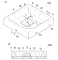
- (A) It is a schematic perspective view which shows the optical semiconductor device which concerns on other embodiment.
- (B) is an optical semiconductor device according to another embodiment, and is a schematic cross-sectional view showing a cross section taken along the line YY of FIG.
- FIG. 3 is a schematic cross-sectional manufacturing process diagram for explaining a manufacturing method of an optical semiconductor device.
- D is a schematic cross-sectional manufacturing process diagram for explaining a manufacturing method of an optical semiconductor device.
- Embodiment 1 Optical semiconductor device (No. 1) 1A and 1B show the structure of the optical semiconductor device 100 of the first embodiment.
- the optical semiconductor device 100 of the present embodiment is referred to as a lead frame 10 (hereinafter, also simply referred to as “lead frame 10”) composed of a light emitting element 2 which is rectangular in a plan view and a pair of plate-shaped metal structures 1 for an optical semiconductor device. ), And a resin molded body 3 in which a part of the lead frame 10 is embedded.
- the resin molded body 3 may be composed of a resin composition containing a thermoplastic resin or a thermosetting resin. Further, the resin molded body 3 can contain a filler such as TiO 2 as described later in the resin composition. This filler may be a reflective material that reflects the light from the light emitting element 2.
- the resin molded body 3 forms a recess having a bottom surface and a side surface, the bottom surface of the recess is composed of a part of a pair of lead frames 10, and the side surface is a side wall portion 31 as a reflective surface having a predetermined inclination angle. Is formed.
- the space between the pair of lead frames 10 is filled with the resin composition constituting the resin molded body 3, and constitutes a part 32 of the bottom surface of the resin molded body 3.
- the resin molded body 3 of the present embodiment has a horizontally long shape in a plan view. A part of a pair of plate-shaped lead frames 10 is exposed as an external terminal portion on the outer surface of the resin molded body 3, and the external terminal portion is bent along the lower surface of the resin molded body 3.
- the light emitting element 2 is mounted on one of the lead frames 10 that constitutes the bottom surface of the recess.
- the light emitting element 2 is covered with a sealing member 5.
- the sealing member 5 includes, for example, a phosphor that converts the wavelength of light from the light emitting element 2 and a sealing material.
- the material of the sealing member 5 preferably contains a translucent resin.
- the phosphor is excited by the light from the light emitting element 2 to wavelength-convert the light from the light emitting element 2 and emit light having at least one emission peak wavelength in a specific wavelength range.
- the light emitting element 2 has a pair of positive and negative electrodes, and the pair of positive and negative electrodes are electrically connected to the pair of lead frames 10 via wires 6, respectively.
- the optical semiconductor device 100 can emit light by receiving electric power from the outside via the pair of lead frames 10.
- the lead frame 10 or the substrate having a metal structure for an optical semiconductor device described in the embodiment described later has a portion that comes into contact with a member formed by using a resin material such as a resin molded body 3 or a sealing member 5. ..
- the package including the metal structure 1 for the optical semiconductor device and the resin molded body 3 constituting the lead frame 10 or the substrate constitutes the present embodiment, and the optical semiconductor device constituting the lead frame 10 or the substrate.
- the adhesion between the metal structure 1 for metal and the resin molded body 3 is improved.
- the metal structure 1 for an optical semiconductor device constituting the lead frame 10 or the substrate will be described in detail later.
- the resin material refers to a material containing at least a resin. Examples of the resin material include a resin composition containing a resin.
- the lead frame 10 made of the metal structure 1 for an optical semiconductor device serves as a mounting member for mounting the light emitting element 2, a reflecting member for reflecting light emitted from the light emitting element 2, and a conductive member electrically connected to the light emitting element 2. It also has the function of. Further, the lead frame 10 may also function as a heat radiating member that dissipates heat generated from the light emitting element 2.
- the lead frame 10 having a metal structure 1 for an optical semiconductor device may be provided below the light emitting element 2 as in the first embodiment, or may be provided in a reflector shape surrounding the light emitting element 2. Further, the lead frame 10 may be a plate-shaped lead frame.
- the metal structure 1 for an optical semiconductor device has the outermost layer 1d of gold, silver, a gold alloy or a silver alloy treated by dipping and / or applying a solution containing a polyallylamine polymer, it adheres to a resin.
- the properties are good, and in the optical semiconductor device 100, for example, the adhesion to the sealing member 5 and the resin molded body 3 can be improved.
- the method for forming the outermost layer 1d may be a known surface treatment and is not particularly limited. For example, plating (electrolytic plating, electroless plating, hot-dip plating, sputtering plating, vapor deposition plating including physical vapor deposition and chemical vapor deposition) ), Plating, etc. can be adopted.
- the content of a filler such as TiO 2 in the resin molded product is increased, or the color rendering property is improved.
- the content of the phosphor in the sealing member may be increased.
- the adhesion between the lead frame of the optical semiconductor device and the resin material tends to decrease.
- the lead frame 10 made of the metal structure 1 for the optical semiconductor device has high adhesion to the resin material, and therefore impurities (titanium oxide, phosphor, etc.) in the resin material.
- the metal structure 1 for an optical semiconductor device has the outermost layer 1d of gold, silver, gold alloy or silver alloy treated by dipping and / or coating a solution containing a polyallylamine polymer, silver or silver alloy. Even when the plating layer of No. 1 is provided as the outermost layer, discoloration due to sulfide or oxidation can be suppressed, a decrease in light beam due to sulfide discoloration or oxidative discoloration can be suppressed, and a high light beam can be maintained.
- Embodiment 2 Metal structure for optical semiconductor device (No. 1)
- the metal structure 1 for an optical semiconductor device can be used for a lead frame or a substrate. Further, by forming the metal structure 1 for an optical semiconductor device as wiring on an insulating substrate, it can be used for a printed circuit board, a ceramic substrate, or the like.
- the substrate is a member capable of comprising the metal structure 1 for an optical semiconductor device, and for example, a lead frame, a metal plate, a wire, a ceramic substrate, a printed circuit board, a flexible substrate, a silicon wafer, a GaAs wafer, and a GaN.
- It may be a ceramic component with a metal terminal such as a wafer or a capacitor, an organic component with a metal terminal such as a resistor, a pin connector, a round connector, a socket, a connector with a resin, or an airtight component such as a laser stem.
- a ceramic component with a metal terminal such as a wafer or a capacitor
- an organic component with a metal terminal such as a resistor, a pin connector, a round connector, a socket, a connector with a resin, or an airtight component such as a laser stem.
- FIG. 2A is a schematic cross-sectional view showing an embodiment of the metal structure 1 for an optical semiconductor device.
- the metal structure 1 for an optical semiconductor device is composed of a nickel or nickel alloy plating layer, a palladium or palladium alloy plating layer, a rhodium or rhodium alloy plating layer, and a platinum or platinum alloy plating layer between the outermost layer and the base material 1a. It can be equipped with at least one selected from the group.
- the metal structure 1 for an optical semiconductor device includes a conductive base material 1a containing, for example, copper or a copper alloy, and a conductive base material 1a containing, for example, copper or a copper alloy on a pair of two surfaces facing each other with the base material 1a as the center.
- a nickel or nickel alloy plating layer 1b and a surface layer 1d of a gold, silver, gold alloy or silver alloy treated by dipping and / or applying a solution containing a polyallylamine polymer on the base material 1a are arranged in this order. Can have.
- the metal structure 1 for an optical semiconductor device uses gold, silver, a gold alloy, or a silver alloy as the outermost layer.
- the Vickers hardness of gold and silver is smaller than the Vickers hardness of nickel, palladium, rhodium, and platinum, and since it is a soft metal, die bonding and wire bonding of the light emitting element 2 are facilitated.
- gold and silver are precious metals and are less likely to be oxidized than nickel, palladium, rhodium and platinum, and thus are less likely to affect solder mounting.
- the outermost surface layer of the metal structure 1 for an optical semiconductor device is a gold or gold alloy layer
- the outermost layer 1d is a silver or silver alloy layer
- a silver or silver alloy plating layer is formed as the outermost layer 1d
- gold or a gold alloy is plated as a base layer of the silver or silver alloy plating layer.
- layer 1c2 This is because gold is a more stable metal than silver. That is, when the outermost layer 1d is a silver or silver alloy layer, a gold or gold alloy plating layer 1c2 may be provided between the nickel or nickel alloy plating layer 1b and the outermost layer 1d.
- the pair of two opposing surfaces of the plate-shaped base material 1a may be referred to as the upper surface or the bottom surface, and the other two opposing surfaces of the plate-shaped base material 1a may be referred to as the side surfaces.
- the outermost surface layer 1d of gold, silver, a gold alloy, or a silver alloy does not have to be provided on all surfaces of the metal structure 1 for an optical semiconductor device. That is, at least a part of the surface of the metal structure 1 for an optical semiconductor device may be gold, silver, a gold alloy, or the outermost surface layer 1d of a silver alloy.
- the lead frame 10 not exposed on the bottom surface of the recess of the resin molded body 3 shown in FIG.
- the second embedded portion 13 in close contact with 5 is treated by dipping and / or applying a solution containing a polyallylamine polymer on its surface to treat gold, silver, gold alloy or It is preferable to have the outermost surface layer 1d of the silver alloy, but the external terminal portion exposed to the outside of the resin molded body 3 and the mounting portion exposed to the bottom surface side of the optical semiconductor device have gold, silver, gold alloy or gold, silver, or gold alloy on the surface thereof.
- the outermost surface layer 1d of the silver alloy may not be provided.
- the outermost layer 1d of gold, silver, gold alloy or silver alloy on a part of the metal structure 1 for an optical semiconductor device as described above, when forming the outermost layer 1d of gold, silver, gold alloy or silver alloy.
- the portion of gold, silver, gold alloy or silver alloy that does not require the outermost layer 1d is masked with a protective tape or the like, and the outermost layer 1d of gold, silver, gold alloy or silver alloy is formed on a part of the surface. Can be done.
- the outermost layer 1d of gold, silver, gold alloy or silver alloy treated by dipping and / or applying a solution containing a polyallylamine polymer is located at a site where it is not in direct contact with the resin molded body 3 or the sealing member 5. If there is, it may be provided on both of a pair of facing two surfaces of the plate-shaped metal structure 1 for an optical semiconductor device, for example, the upper surface and the bottom surface as in the present embodiment, and may be provided only on one surface and another. It does not have to be provided on the surface. Further, it may be provided only on a part of one surface.
- the outermost layer 1d of gold, silver, a gold alloy or a silver alloy treated by dipping and / or applying a solution containing a polyallylamine polymer may have the same thickness over the entire provided region. , The thickness may be different. By making the thickness different, the cost can be reduced more effectively.
- the outermost surface layer 1d of gold, silver, a gold alloy or a silver alloy treated by dipping and / or applying a solution containing a polyallylamine polymer is provided on the upper surface and the bottom surface of the metal structure 1 for an optical semiconductor device. The thickness on one side may be thicker than the other.
- the outermost layer 1d of gold, silver, gold alloy or silver alloy treated by dipping and / or applying a solution containing a polyallylamine polymer to a portion in direct contact with the resin molded body 3 or the sealing member 5 is provided.
- the metal structure 1 for an optical semiconductor device has a base material 1a having a surface layer 1d of gold, silver, a gold alloy, or a silver alloy treated by dipping and / or applying a solution containing a polyallylamine polymer.
- the base material 1a is used as a material for determining the rough shape of the metal structure 1 for an optical semiconductor device.
- the material of the base material 1a is not particularly limited, and copper, iron, alloys thereof, clad material (for example, copper / iron-nickel alloy / copper laminate) and the like can be preferably used.
- a copper alloy an alloy of copper and iron, tin, nickel, etc. can be adopted, and the copper content in that case is preferably 77.5% by mass or more and 99.5% by mass or less. ..
- an iron alloy an alloy of iron and nickel, cobalt or the like can be adopted, and the iron content in that case is preferably 55.0% by mass or more and 99.9% by mass or less. Copper and copper alloys are excellent in heat dissipation and can be preferably used.
- plate-shaped copper and copper alloys are preferable because they are excellent in terms of mechanical properties, electrical properties, workability, and the like. Since the clad material can suppress the coefficient of linear expansion to a low level, the reliability of the optical semiconductor device 100 can be improved.
- the thickness, shape, etc. of the base material 1a can be variously selected according to the shape, etc. of the optical semiconductor device 100. For example, it may have a plate-like shape, a lump-like shape, a film-like shape, or the like. Further, the wiring pattern may be provided on ceramic or the like by printing or the like, or the formed wiring pattern may be plated with copper or a copper alloy.
- the flatness of the base material 1a is preferably as high as possible.
- the surface roughness Ra of the base material 1a is preferably 0.5 ⁇ m or less.
- a nickel or nickel alloy plating layer 1b provided on the base material 1a as needed a palladium or palladium alloy plating layer provided as needed, a rhodium or rhodium alloy plating layer, a platinum or platinum alloy plating layer, etc.
- the flatness of the noble metal plating layer 1c1 made of the material and the outermost surface layer 1d of gold, silver, gold alloy or silver alloy can be further improved.
- the flatness of the base material 1a when the flatness of the base material 1a is high, the flatness of the outermost layer 1d of gold, silver, gold alloy or silver alloy having a thickness of 0.01 ⁇ m or more and 0.5 ⁇ m or less can be also high, and the optical semiconductor device can be increased.
- the reflectance of the metal structure 1 can be satisfactorily increased.
- the flatness of the base material 1a can be improved by performing treatments such as rolling, physical polishing, and chemical polishing, and by plating the same type of material as the material constituting the base material 1a, the base material 1a can be flattened.
- the flatness of 1a can also be increased. For example, in the case of the base material 1a made of a copper alloy, copper alloy plating can be performed to improve the flatness of the base material 1a.
- the metal structure 1 for an optical semiconductor device of the present embodiment preferably has a nickel or nickel alloy plating layer 1b on a base material 1a.
- the thickness of the nickel or nickel alloy plating layer 1b is preferably 0.5 ⁇ m or more and 10 ⁇ m or less, and more preferably 1 ⁇ m or more and 10 ⁇ m or less.
- the metal contained in the base material 1a to the base material 1a is a base layer of a palladium or palladium alloy plating layer, a rhodium or rhodium alloy plating layer, and platinum.
- the noble metal plating layer 1c1 composed of a platinum alloy plating layer or the like, or the outermost layer 1d of gold, silver, a gold alloy or a silver alloy.
- the thickness of the nickel or nickel alloy plating layer 1b is 10 ⁇ m or less, the raw material and the manufacturing cost can be reduced.
- the material of the nickel or nickel alloy plating layer 1b for example, in addition to nickel, alloys such as nickel phosphorus, nickel tin, and nickel cobalt can be used.
- the nickel content is preferably 90.0% by mass or more and 99.0% by mass or less.
- FIG. 2B is a schematic cross-sectional view showing another embodiment of the metal structure 1 for an optical semiconductor device.
- the metal structure 1 for an optical semiconductor device may have a base layer 1c between the nickel or nickel alloy plating layer 1b and the outermost layer 1d of gold, silver, gold alloy or silver alloy.
- the base layer 1c preferably has a noble metal plating layer 1c1 composed of a palladium or palladium alloy plating layer, a rhodium or rhodium alloy plating layer, a platinum or platinum alloy plating layer, or the like.
- the metal structure 1 for an optical semiconductor device has a pair of two surfaces facing each other with the base material 1a as the center, and on the base material 1a, for example, a nickel or nickel alloy plating layer 1b and a poly.
- the outermost layer 1d of gold, silver, gold alloy or silver alloy treated by dipping and / or coating a solution containing an allylamine polymer can be provided in this order.
- the metal structure 1 for an optical semiconductor device has a palladium or palladium alloy plating layer between the above-mentioned nickel or nickel alloy plating layer 1b and the outermost layer 1d of gold, silver, gold alloy or silver alloy.
- a noble metal plating layer 1c1 made of a rhodium or a rhodium alloy plating layer, a platinum or a platinum alloy plating layer or the like is provided. That is, the metal structure 1 for an optical semiconductor device is a noble metal plating composed of a base material 1a, a nickel or nickel alloy plating layer 1b, a palladium or palladium alloy plating layer, a rhodium or rhodium alloy plating layer, a platinum or platinum alloy plating layer, or the like.
- the layer 1c1 and the outermost layer 1d of gold, silver, a gold alloy, or a silver alloy treated by dipping and / or applying a solution containing a polyallylamine polymer are laminated in this order.
- the metal structure 1 for an optical semiconductor device has, for example, a nickel or nickel alloy plating layer 1b and, if necessary, so as to wrap around the base material 1a on two pairs of four surfaces facing each other with the plate-shaped base material 1a as the center.
- Silver, gold alloy, or the outermost surface layer 1d of the silver alloy may be provided in this order.
- the metal structure 1 for the optical semiconductor device is made of gold, silver, a gold alloy, or silver. It has an alloy as the outermost layer.
- the outermost surface layer of the metal structure 1 for an optical semiconductor device is a gold or gold alloy layer
- the outermost layer 1d is a silver or silver alloy layer
- a silver or silver alloy plating layer is formed as the outermost layer 1d
- gold or a gold alloy is plated as a base layer of the silver or silver alloy plating layer. It is preferable to form layer 1c2.
- the base layer 1c may be only the above-mentioned precious metal plating layer 1c1 or only the gold or gold alloy plating layer 1c2. Further, the gold or gold alloy plating layer 1c2 may be laminated on the noble metal plating layer 1c1, and the noble metal plating layer 1c1 and the gold or gold alloy plating layer 1c2 can be combined to form the base layer 1c.
- the metal structure 1 for an optical semiconductor device of the present embodiment comprises a palladium or palladium alloy plating layer, a rhodium or rhodium alloy plating layer, a platinum or platinum alloy plating layer, or the like as a base layer in contact with the nickel or nickel alloy plating layer 1b. It is preferable to have the noble metal plating layer 1c1.
- a nickel or nickel alloy plating layer 1b is provided on the base material 1a, and a palladium or palladium alloy plating layer, rhodium or rhodium alloy is provided as a second base layer on the base material 1a.
- a noble metal plating layer 1c1 composed of a plating layer, platinum or a platinum alloy plating layer, and further laminate gold, silver, the outermost layer 1d of a gold alloy or a silver alloy in this order.
- the copper contained in the base material 1a is further suppressed from diffusing into the outermost layer 1d of gold, silver, a gold alloy or a silver alloy. It is possible to improve the adhesion of each of the laminated layers. Further, since the diffusion of copper contained in the base material 1a is further suppressed, the wire bonding property can be further improved when the metal structure 1 for an optical semiconductor device is used as the lead frame 10.
- the thickness of the noble metal plating layer 1c1 is preferably 0.01 ⁇ m or more and 0.3 ⁇ m or less, more preferably 0.02 ⁇ m or more and 0.2 ⁇ m or less, and further preferably 0.03 ⁇ m or more and 0.1 ⁇ m or less.
- the metal contained in the base metal 1a diffuses to the outermost layer 1d of gold, silver, gold alloy or silver alloy. This can be further suppressed, and when the metal structure 1 for an optical semiconductor device is used as the lead frame 10, the wire bonding property can be further improved.
- the material of the palladium or palladium alloy plating layer for example, in addition to palladium, alloys such as nickel, phosphorus, cobalt, and copper can be used.
- the palladium content is preferably 75.0% by mass or more and 97.0% by mass or less.
- alloys such as nickel, cobalt, and platinum can be used.
- the rhodium content is preferably 75.0% by mass or more and 99.0% by mass or less.
- the material of the platinum or platinum alloy plating layer for example, in addition to platinum, alloys such as nickel, cobalt, and copper can be used.
- the platinum content is preferably 75.0% by mass or more and 99.0% by mass or less.
- the noble metal plating layer 1c1 which is the base layer of the outermost layer 1d of gold, silver, gold alloy or silver alloy serves as a layer having both a role of preventing sulfurization and preventing the diffusion of the metal contained in the base material 1a into other layers. May be good. Thereby, the cost can be further reduced. For example, gold does not easily react with the sulfur component and has a high effect of preventing the diffusion of the metal contained in the base material 1a, so that it can be preferably used.
- the metal structure 1 for an optical semiconductor device is preferably a substantially flat lead frame 10 as shown in FIGS. 3A and 3B described later, for example.
- the reliability of the metal structure 1 for an optical semiconductor device as a reflective member can be improved.
- the nickel or nickel alloy plating layer 1b is slightly more brittle than copper, iron, alloys thereof, clad material (for example, copper / iron nickel alloy / copper laminate) used as the base material 1a, the nickel or nickel alloy plating layer
- the metal structure 1 for an optical semiconductor device including 1b is preferably used as a flat plate without being bent.
- Embodiment 4 Optical semiconductor device (No. 2) 3A and 3B show the structure of the optical semiconductor device 200 of the fourth embodiment.
- the optical semiconductor device 200 of the present embodiment has a lead frame 10 having no bent portion.
- the members common to the optical semiconductor device 100 of the first embodiment are designated by the same reference numerals.
- Light emitting element 2 As the light emitting element 2, a semiconductor light emitting element having an arbitrary wavelength can be selected.
- a nitride semiconductor such as InGaN, GaN, or AlGaN, or one using GaP can be used.
- the red light emitting element GaAlAs, AlInGaP and the like can be used.
- a light emitting element 2 made of a material other than this can also be used. The composition, emission color, size, number, and the like of the light emitting element 2 to be used can be appropriately selected according to the purpose.
- the optical semiconductor device 100 or the optical semiconductor device 200 includes a member capable of wavelength conversion
- a nitride semiconductor capable of emitting a short wavelength capable of efficiently exciting the member capable of wavelength conversion is preferably mentioned.
- Various emission wavelengths can be selected depending on the material of the semiconductor layer and the mixed crystal ratio thereof.
- the light emitting element 2 can output not only light in the visible light region but also ultraviolet rays and infrared rays.
- the light emitting element 2 is preferably mounted on a lead frame 10 made of a metal structure 1 for an optical semiconductor device. Thereby, the light extraction efficiency of the optical semiconductor device 100 or the optical semiconductor device 200 can be further improved.
- the light emitting element 2 preferably has positive and negative electrodes that are electrically connected to the conductive member. These positive and negative electrodes may be provided on one surface side, or may be provided on both the upper and lower surfaces of the light emitting element 2.
- the connection with the conductive member may be made by the joining member 4 and the wire 6 described later, or by flip-chip mounting.
- the resin molded body 3 is a member made of a resin composition that integrally holds a pair of lead frames 10.
- the plan view shape of the resin molded body 3 may be a substantially rectangular shape in which a pair of opposite sides as shown in FIG. 1A is longer than the other facing sides, and a rectangular shape as shown in FIG. 3A. It may be.
- the resin molded body 3 may have a polygonal shape or a shape obtained by combining them.
- the side wall portion 31 of the recess may have an inclined surface whose inner side surface is provided at an inclined angle with respect to the bottom surface as shown in FIG. 3B, and has a substantially vertical angle.
- the lead frame 10 is provided inside the recess. It is preferable that the space between the pair of lead frames 10 and 10 is filled with the resin composition constituting the resin molded body 3 to form a part 32 of the bottom surface of the resin molded body 3.
- the resin molded body 3 can be formed by using a resin composition containing a thermosetting resin or a thermoplastic resin.
- a resin composition containing a thermosetting resin As the composition containing the thermosetting resin, a resin having a lower gas permeability than the resin used for the sealing member 5 is preferable, and specifically, an epoxy resin composition, a silicone resin composition, and a silicone-modified epoxy resin.
- modified epoxy resin compositions such as, modified silicone resin compositions such as epoxy modified silicone resins, polyimide resin compositions, modified polyimide resin compositions, urethane resins, modified urethane resin compositions and the like.
- the composition containing the thermoplastic resin a resin having low viscosity and easy flow is preferable, and specifically, polyamide, polyphthalamide (PPA), polycarbonate resin, polyphenylene terephide (PPS), liquid crystal polymer (LCP), and the like.
- examples thereof include acrylonitrile butadiene styrene copolymer resin (ABS resin), phenol resin, acrylic resin, polybutylene terephthalate resin (PBT resin) and the like.
- the resin composition constituting the resin molded body 3 includes TiO 2 , SiO 2 , Al 2 O 3 , MgO, MgCO 3 , CaCO 3 , Mg (OH) 2 , Ca (OH) 2, etc. as fillers.
- the inorganic particles as a filler in the resin composition constituting the resin molded body 3, the light transmittance of the resin molded body 3 can be adjusted.
- the amount of TiO 2 which is a white component in order to improve the reflectance of the resin material for the purpose of increasing the total light beam of the light emitting device for example, when the total amount of the resin composition is 100% by mass, the content of TiO 2 is contained.
- the amount is 20% by mass or more and 60% by mass or less
- the adhesion between the metal structure 1 for the optical semiconductor device and the resin material may be lowered.
- the member holding the lead frame 10 may be made of an inorganic substance such as ceramic, glass, or metal.
- the optical semiconductor device 100 or the optical semiconductor device 200 can be obtained with little deterioration and high reliability.
- the joining member 4 is a member for fixing and mounting the light emitting element 2 to the lead frame 10.
- the same material as the outermost layer 1d of copper, silver, gold particles, gold, silver, gold alloy or silver alloy can be used.
- an epoxy resin composition, a silicone resin composition, a polyimide resin composition, a modified resin thereof, a hybrid resin, or the like can be used.
- a metal layer having high reflectance such as an aluminum film or a silver film or a dielectric reflective film is provided on the mounting surface of the light emitting element 2 in consideration of deterioration due to light or heat from the light emitting element 2. be able to.
- the sealing member 5 is provided so as to cover each member of the light emitting element 2, the lead frame 10, the wire 6, and the protective film described later.
- the sealing member 5 By providing the sealing member 5 in the optical semiconductor device 100 or the optical semiconductor device 200, the coated member can be protected from dust, moisture, external force, and the like, and the reliability of the optical semiconductor device can be improved. ..
- the sealing member 5 on the protective film after forming the protective film the protective film can be protected, so that the reliability of the optical semiconductor device is enhanced.
- the sealing member 5 preferably has a light-transmitting property capable of transmitting light from the light emitting element 2 and a light resistance that is not easily deteriorated by them.
- Specific materials used for the sealing member 5 include a silicone resin composition, a modified silicone resin composition, a modified epoxy resin composition, a fluororesin composition, and the like, which have translucency capable of transmitting light from a light emitting element.
- An insulating resin composition can be mentioned.
- a hybrid resin containing at least one resin having a siloxane skeleton as a base such as dimethyl silicone, phenyl silicone having a low phenyl content, and a fluorine-based silicone resin, can also be used.
- the sealing member 5 is formed by using a potting (dropping) method, a compression molding method, a printing method, a transfer molding method, a jet dispensing method, a spray coating, or the like. be able to.
- the potting method is preferable, and when the optical semiconductor device uses a flat plate-shaped substrate, the compression molding method or the transfer molding method is preferable.
- the sealing member 5 is preferably provided so as to fill the recessed portion of the resin molded body 3.
- the shape of the outer surface of the sealing member 5 can be variously selected according to the light distribution characteristics required for the optical semiconductor device 100 and the like. For example, by making the upper surface a convex lens shape, a concave lens shape, a Fresnel lens shape, a rough surface, or the like, the directivity characteristics and the light extraction efficiency of the optical semiconductor device can be adjusted.
- the sealing member 5 can also contain a colorant, a light diffusing material, a light reflecting material, various fillers, a wavelength conversion member, and the like.
- the wavelength conversion member is a material that converts the light of the light emitting element 2 into wavelength.
- the yttrium aluminum garnet phosphor (hereinafter referred to as "YAG: Ce”), which is a kind of aluminum oxide phosphor, is preferable as the wavelength conversion member. Used for. Since the YAG: Ce phosphor absorbs a part of the blue light from the light emitting element and emits the yellow light as a complementary color, it is relatively easy to use a high-output optical semiconductor device that emits a white mixed color light. Can be formed into.
- the wire 6 connects the light emitting element 2 and a conductive member such as the lead frame 10.
- a conductive member such as the lead frame 10.
- gold, silver, aluminum, copper, alloys thereof and the like are preferably used.
- a wire 6 having a coating layer provided on the surface of the core with a material different from that of the core for example, a wire 6 provided with a coating layer of palladium, palladium gold alloy or the like on the surface of the copper core can also be used.
- the material of the wire 6 is preferably selected from any one of highly reliable gold, silver, and silver alloy. Further, in particular, silver or a silver alloy having a high light reflectance is preferable.
- the wire 6 is covered with a protective film. This makes it possible to further prevent sulphurization and disconnection of the wire containing silver, and further enhance the reliability of the optical semiconductor device 100.
- the base material 1a of the metal structure for the optical semiconductor device constituting the lead frame 10 contains copper and the wire 6 is made of silver or a silver alloy
- the metal structure 1 for the optical semiconductor device is a nickel or nickel alloy plating layer. By providing 1b, the formation of a local battery between copper and silver can be suppressed. As a result, deterioration of the lead frame 10 and the wire 6 is further suppressed, and a more reliable optical semiconductor device can be obtained.
- the wire 6 may include the metal structure 1 for an optical semiconductor device, similarly to the lead frame 10 having the metal structure 1 for an optical semiconductor device described above.
- the wire 6 since it has the outermost layer 1d obtained by dipping and / or applying a solution containing a polyallylamine polymer, it has good adhesion to a resin, and in the optical semiconductor device 100 or the optical semiconductor device 200, for example, it is sealed. The adhesion with the stop member 5 can be improved.
- the optical semiconductor device 100 or the optical semiconductor device 200 may further include a protective film.
- the protective film can cover at least the outermost layer 1d of gold, silver, a gold alloy, or a silver alloy provided on the surface of the metal structure 1 for an optical semiconductor device constituting the lead frame 10.
- the protective film is a member that suppresses discoloration or corrosion of the outermost layer 1d of gold, silver, a gold alloy, or a silver alloy on the surface of the metal structure 1 for an optical semiconductor device that mainly constitutes the lead frame 10.
- the protective film is optionally provided with the surface of a member other than the lead frame 10 or the substrate such as the light emitting element 2, the joining member 4, and the resin molded body 3, and the outermost layer 1d of gold, silver, gold alloy, or silver alloy.
- the surface of the metal structure 1 for an optical semiconductor device which has not been provided may be coated.
- the protective film is provided so as to cover the wire 6 or the outermost layer 1d. Is preferable. This makes it possible to further prevent sulphurization and disconnection of the wire containing silver, and further enhance the reliability of the optical semiconductor device 100 or the optical semiconductor device 200.
- the protective film is preferably formed by a sputtering method, a chemical vapor deposition method, or an atomic layer deposition method (hereinafter, also referred to as ALD (Atomic Layer Deposition)).
- ALD atomic layer deposition
- a very uniform protective film can be formed, and the formed protective film is denser than the protective film obtained by other film forming methods. Therefore, for example, a lead. It is possible to very effectively prevent sulfide and discoloration of the outermost layer 1d of the metal structure 1 for an optical semiconductor device constituting the frame 10.
- Materials for the protective film include Al 2 O 3 , SiO 2 , TiO 2 , ZrO 2 , ZnO, Nb 2 O 5 , MgO, In 2 O 3 , Ta 2 O 5 , HfO 2 , SeO, Y 2 O 3 , Examples thereof include oxides such as SnO 2 , nitrides such as AlN, TiN and ZrN, and fluorides such as ZnF 2 and SrF 2. These may be used alone or in combination. Alternatively, they may be laminated.
- the optical semiconductor device 100 or the optical semiconductor device 200 can be provided with various members in addition to the above.
- a Zener diode can be mounted as a protection element.
- a lead frame 10 having a metal structure 1 for an optical semiconductor device according to a second or third embodiment is prepared. Specifically, for example, a copper metal plate constituting the base material 1a of the metal structure 1 for an optical semiconductor device is punched, and as described later in the method for manufacturing the metal structure 1 for an optical semiconductor device, if necessary.
- a noble metal plating layer 1c1 composed of nickel or nickel alloy plating layer 1b, palladium or palladium alloy plating layer, rhodium or rhodium alloy plating layer, platinum or platinum alloy plating layer, etc., and gold, silver, gold alloy or silver alloy, if necessary.
- a lead frame which is a lead frame formed by forming the outermost layer 1d of the above, dipping and / or applying it in a solution containing a polyallylamine polymer, and then washing with water or hot water (washing) as necessary and drying.
- the resin molded body 3 can be molded by the transfer molding method so as to be in contact with the lead frame 10 using the metal structure 1 for an optical semiconductor device.
- the resin molded body 3 may be formed so that the pair of lead frames 10 are each exposed on the bottom surface of the recess of the resin molded body 3. That is, the lead frame 10 can be exposed on the bottom surface of the recess of each resin molded body 3.
- the light emitting element 2 can be mounted via the joining member 4 in the region where the light emitting element 2 of the lead frame 10 on which the resin molded body 3 is formed is mounted. Then, the light emitting element 2 and the lead frame 10 can be connected by a wire. After that, the sealing member 5 can be provided in each recess of the resin molded body 3.
- the lead frame 10 and the resin molded body 3 as shown in FIG. 4D can be cut with a dicing saw or the like and separated into individual optical semiconductor devices as shown in FIGS. 3A and 3B.
- the cross section of the lead frame 10 is exposed on the outer surface of the optical semiconductor device 200.
- a base material 1a such as copper of the metal structure 1 for an optical semiconductor device constituting the lead frame 10, a nickel or nickel alloy plating layer 1b if necessary, and a palladium or palladium alloy plating layer if necessary.
- a noble metal plating layer 1c1 composed of a rhodium or rhodium alloy plating layer, a platinum or platinum alloy plating layer, and the outermost layer of a treated gold, silver, gold alloy, or silver alloy that has been immersed and / or coated in a solution containing a polyallylamine polymer. 1d is exposed.
- Embodiment 5 Method for manufacturing metal structure for optical semiconductor device Next, a method for manufacturing a metal structure for optical semiconductor device will be described.
- the method for manufacturing a metal structure for an optical semiconductor device is as follows. (1) At least one selected from the group consisting of gold, silver, gold alloys and silver alloys (preferably at least one selected from the group consisting of gold, silver, gold alloys and silver alloys) in part or on the entire surface.
- a treatment step of dipping and / or applying a solution containing a polyallylamine polymer to a substrate having an outermost layer (gold, silver, gold alloy or outermost surface layer 1d of a silver alloy) having (plating) is provided.
- the plating is a metal film formed by, for example, wet plating such as electrolytic plating and electroless plating, and dry plating such as hot-dip plating, sputtering plating, and vapor deposition plating including physical vapor deposition and chemical vapor deposition.
- the substrate may include an outermost layer having at least one selected from the group consisting of gold, silver, gold alloys and silver alloys, and the outermost layer does not have to be a metal film formed by surface treatment. ..
- the substrate itself may be at least one selected from the group consisting of gold, silver, gold alloys and silver alloys.
- the substrate can also be subjected to the above step after forming a step at a predetermined position by wet etching and forming the step.
- a nickel or nickel alloy plating layer 1b if necessary, a palladium or palladium alloy plating layer, a rhodium or rhodium alloy plating layer, platinum or platinum alloy plating. It is preferable to form the noble metal plating layer 1c1 composed of layers and the like. Therefore, before performing the above-mentioned step (1), a step of forming a nickel or nickel alloy plating layer 1b on the base material 1a as needed, and a step of forming the nickel or nickel alloy plating layer 1b on the nickel or nickel alloy plating layer 1b as needed.
- the steps of forming the outermost layer 1d of gold, silver, gold alloy or silver alloy are the step of forming the plating layer of gold or gold alloy and silver.
- the thickness of the gold or gold alloy plating layer 1c2 can be 0.003 ⁇ m or more and 0.5 ⁇ m or less.
- the outermost layer 1d is not necessarily limited to plating, and may be a metal film formed by thermal spraying.
- the step of forming each of these layers is easy, it is preferable to carry out by the method of forming a metal film by the above-mentioned plating, and more preferably by electrolytic plating or electroless plating. Among them, electrolytic plating is preferable because the layer formation speed is high and mass productivity can be improved.
- the base material 1a Before forming each of the above layers, the base material 1a can be pretreated.
- the pretreatment include acid treatment of dilute sulfuric acid, dilute nitric acid, dilute hydrochloric acid and the like, alkali treatment of sodium hydroxide and the like, and these may be performed once or several times with the same treatment or a combination of different treatments. .. When the pretreatment is performed several times, it is preferable to wash with running water using pure water after each treatment.
- the base material 1a is a metal plate made of copper or a copper alloy, it is preferable to use dilute sulfuric acid for the pretreatment.
- the base material 1a is a metal plate made of iron or an iron alloy, it is preferable to use dilute hydrochloric acid for the pretreatment.
- the nickel or nickel alloy plating layer 1b when the material constituting the plating layer is pure nickel, it can be formed by electrolytic plating using, for example, a plating solution containing nickel sulfamate. When a nickel-phosphorus alloy is used, it can be formed by electroless plating using a nickel hypophosphate plating solution.
- the noble metal plating layer 1c1 composed of palladium or palladium alloy plating layer, rhodium or rhodium alloy plating layer, platinum or platinum alloy plating layer, etc.
- the material constituting the plating layer is palladium or palladium alloy, for example. It can be formed by electrolytic plating using a plating solution containing tetraammine-palladium chloride.
- the material constituting the plating layer is rhodium or a rhodium alloy, it can be formed by electrolytic plating using, for example, a plating solution containing rhodium sulfate.
- the material constituting the plating layer is platinum or a platinum alloy, it can be formed by electrolytic plating using, for example, a plating solution containing a dinitrodiamine platinum salt.
- the outermost surface layer 1d of gold, silver, a gold alloy, or a silver alloy is provided on the surface of the metal structure 1 for an optical semiconductor device.
- the thickness of the outermost surface layer 1d of gold, silver, a gold alloy or a silver alloy is 0.003 ⁇ m or more and 0.5 ⁇ m or less, preferably 0.01 ⁇ m or more and 0.3 ⁇ m or less.
- the die bonding property with the light emitting element 2 and the wire bonding property with the wire 6 can be further improved.
- the thickness of the outermost surface layer 1d of gold, silver, a gold alloy or a silver alloy is 0.5 ⁇ m or less, the amount of expensive precious metal used can be further reduced, and the cost can be further reduced.
- the gold content is preferably 75.0% by mass or more and 99.9% by mass or less, and when a silver alloy is used, the silver content is 75.0% by mass. It is preferably% or more and 99.9% by mass or less.
- the outermost surface layer 1d is a gold or gold alloy layer
- potassium gold cyanide or gold cyanide is added at a metal gold concentration of 0.5 g / L or more and 10 g / L. It is preferable to use a plating solution containing L or less and containing 30 g / L or more and 150 g / L or less of an electrically conductive salt.
- a gold-silver alloy plating or a gold-copper alloy plating layer can be obtained by adding silver potassium cyanide, potassium copper cyanide, or the like as an alloy metal in an amount of 1 g / L or more and 5 g / L or less, respectively.
- the outermost surface layer 1d is a silver or silver alloy layer, and when the silver or silver alloy layer is formed by electrolytic plating, it contains 20 g / L or more and 80 g / L or less of silver potassium cyanide or silver cyanide as metallic silver. It is preferable to use a plating solution containing 50 g / L or more and 150 g / L or less of free potassium cyanide or an electrically conductive salt. Further, a selenium compound or an organic sulfur compound can be further added to this plating solution as a brightener.
- silver alloy plating it is possible to obtain a silver-gold alloy plating or a silver-copper alloy plating layer by adding 5 g / L or more and 20 g / L or less of potassium gold cyanide or potassium copper cyanide as an alloy metal, respectively. it can.
- the plating solution preferably contains 5 g / L or more and 150 g / L or less of one or more kinds of electrically conductive salts such as cyanate, carbonate, phosphate, nitrate, citrate, and sulfate.
- electrically conductive salts such as cyanate, carbonate, phosphate, nitrate, citrate, and sulfate.
- the electric conductive salt contained in the plating solution is 5 g / L or more and 150 g / L or less, the viscosity of the plating solution does not become excessive, and the so-called carry-out of the plating solution by the object to be plated is reduced. It can be economically plated with gold, silver, gold alloys or silver alloys.
- the cyanide salt include potassium cyanide and sodium cyanide.
- the carbonate include potassium carbonate, sodium carbonate, ammonium carbonate and the like.
- the phosphate include potassium phosphate, sodium phosphate, ammonium phosphate, potassium pyrophosphate and the like.
- Examples of the nitrate include potassium nitrate, sodium nitrate, ammonium nitrate and the like.
- Examples of the citrate include potassium citrate, sodium citrate, ammonium citrate and the like.
- Examples of the sulfate include potassium sulfate, sodium sulfate and the like.
- the temperature of the plating solution is 20 ° C. or higher and 70 ° C. or lower, and the electrode is made of gold, silver or gold-silver alloy. becomes soluble electrode or, stainless steel or platinum, using a platinum-coated titanium electrode, a cathode current density of the conductive substrate is a 0.1 a / dm 2 or more 10A / dm 2 or less, 10 minutes plating time is 5 seconds or more It is preferable to perform electrolytic plating under the following conditions.
- the gold, silver, gold alloy or silver alloy layer which is the outermost surface layer 1d is not a metal film formed by plating, spraying or the like, for example, a metal plate or a wire, it is formed or prepared by a conventional method. be able to.
- the outermost layer 1d of gold, silver, a gold alloy or a silver alloy is treated by dipping and / or applying a solution containing a polyallylamine polymer.
- the film containing the polyallylamine polymer adheres to the substrate including the outermost layer 1d of gold, silver, a gold alloy or a silver alloy.
- the thickness of the film containing the polyallylamine polymer is preferably 10 nm or more and 500 nm or less. By setting the thickness of the film containing the polyallylamine polymer to 500 nm or less, die bonding, wire bonding, or solder mounting of the light emitting device can be further improved. Further, by setting the thickness of the film containing the polyallylamine polymer to 10 nm or more, the adhesion between the metal structure 1 for an optical semiconductor device and the resin material can be further improved.
- the polyallylamine polymer is not particularly limited, but usually, a homopolymer of allylamine, which is a primary amine, is assumed, and specifically, it is assumed.
- n 25 to 440.
- examples thereof include a polyallylamine polymer represented by. These polyallylamine polymers can be used alone or in combination of two or more.
- the weight average molecular weight of the polyallylamine polymer described above is preferably 1600 or more and 25,000 or less, and more preferably 3000 or more and 18,000 or less, from the viewpoint of adhesion to the resin material.
- polyallylamine polymer As the polyallylamine polymer as described above, a known or commercially available product can be used, or a polymer can be used. When a commercially available product is used, it can be easily obtained because it is sold by Nittobo Medical Co., Ltd. under the trade name PAA (registered trademark).
- this polyallylamine polymer is water-soluble, aqueous solutions of various concentrations can be produced.
- the total amount of the solution containing the polyallylamine polymer is 100% by mass, and the aqueous solution is preferably 0.01% by mass or more and 1.0% by mass or less. It is more preferable to use an aqueous solution of 05% by mass or more and 0.5% by mass or less.
- the concentration of the solution containing the polyallylamine polymer By setting the concentration of the solution containing the polyallylamine polymer to 1.0% by mass or less, not only the adhesion to the resin material is improved, but also the viscosity of the aqueous solution is not made too high, and the metal structure for optical semiconductor devices is used. It is more economical because the treatment liquid is less likely to be taken out together with 1.
- the solution containing the polyallylamine polymer may contain a triazine compound. That is, the membrane containing the polyallylamine polymer adhering to the substrate may contain a triazine compound.
- the adhesion to the resin material can be further improved. Since the triazine compound has excellent adhesion to gold, the adhesion to the resin material can be particularly improved when a gold or gold alloy layer is used as the outermost layer 1d.
- a triazine thiol compound is preferable from the viewpoint of easily improving the adhesion with the resin material.
- Y represents a nitrogen atom or a sulfur atom.
- R 1 , R 2 and R 3 are the same or different and represent a hydrogen atom, an alkali metal atom or a substituted or unsubstituted alkyl group.
- m indicates 1 or 2
- m indicates 2 when Y is a nitrogen atom
- m indicates 1 when Y is a sulfur atom.
- Examples thereof include triazine compounds represented by.
- examples of the alkali metal atom represented by R 1 , R 2 and R 3 include a lithium atom, a sodium atom, a potassium atom, a cesium atom and the like.
- the alkyl groups represented by R 1 , R 2 and R 3 include methyl group, ethyl group, n-propyl group, isopropyl group, n-butyl group, isobutyl group and sec-butyl group. Examples thereof include alkyl groups having 1 to 10 carbon atoms (particularly 1 to 6) such as tert-butyl groups. These alkyl groups may have 1 to 3 substituents such as a halogen atom (chlorine atom, bromine atom, iodine atom, etc.).
- triazine compounds may be used alone or in combination of two or more.
- triazine compounds known or commercially available products can be used.
- the sodium salt of 1,3,5-triazine-2,4,6-thiol is sold by Sankyo Kasei Co., Ltd. under the trade name of Santhiol, and is easily available and water-soluble. Therefore, it is preferable because a treatment liquid having an appropriate concentration can be prepared.
- the above-mentioned triazine compound is composed of 100% by mass of the total amount of the solution containing the polyallylamine polymer.
- the content is preferably 0.01% by mass or more and 1.0% by mass or less, and more preferably 0.05% by mass or more and 0.5% by mass or less.
- the concentration of the solution containing the triazine compound By setting the concentration of the solution containing the triazine compound to 1.0% by mass or less, not only the adhesion to the resin material is improved, but also the viscosity of the aqueous solution is not made too high, together with the metal structure 1 for an optical semiconductor device. It is more economical because the treatment liquid is less likely to be taken out.
- Triazine compounds have excellent adhesion to gold and silver (especially gold), and triazine thiol compounds have good adhesion to gold due to the intermolecular force between gold and S (sulfur), but their effectiveness is effective when washed with water. There is a concern that it will weaken.
- the polyallylamine polymer has a large molecular weight, and the solution containing the polyallylamine polymer is sticky. Therefore, the polyallylamine polymer adheres to the surface of the outermost layer 1d of gold, silver, a gold alloy, or a silver alloy by the treatment of the present embodiment. It is easy to form a film containing an allylamine polymer.
- the film containing the polyallylamine polymer improves the adhesion between the outermost layer 1d of gold, silver, a gold alloy or a silver alloy and the resin material, and when the film containing the polyallylamine polymer contains a triazine compound. Since the film containing the polyallylamine polymer retains the triazine compound, it is presumed that a better effect can be obtained in improving the adhesion.
- an appropriate anionic surfactant and cationic surfactant are used in order to further improve the wettability and dissolution stability of gold, silver, a gold alloy or a silver alloy to the outermost layer 1d.
- Activators, nonionic surfactants and the like can also be added.
- an appropriate organic solvent or an appropriate pH buffer can be added.
- the pH buffer include boric acid or a salt thereof, diphosphate or a salt thereof, phosphoric acid or a salt thereof, or citric acid or a salt thereof.
- a concentrated solution may be prepared in advance, and when used in a processing apparatus, this concentrated solution may be appropriately diluted with water before use.
- the above-mentioned solution containing the polyallylamine polymer is particularly useful for being used for improving the adhesion between the lead frame 10 in the optical semiconductor device 100 or the optical semiconductor device 200 and the adjacent resin molded product 3. is there.
- a method for treating a solution containing a polyallylamine polymer with respect to gold, silver, a gold alloy or a silver alloy layer it is preferable to perform treatment by dipping and / or coating.
- the gold, silver, gold alloy or silver alloy layer may be all immersed in the solution containing the polyallylamine polymer, or only the portion in contact with the resin material may be immersed.
- the coating treatment particularly the spraying treatment
- the solution containing the polyallylamine polymer may be coated by a known means, or the spraying treatment (spraying treatment or the like) may be performed by a known means.
- the gold, silver, gold alloy or silver alloy layer may be sprayed at a right angle, or may be sprayed horizontally or at an angle. Further, it may be a spray jet or a shower. Further, both the dipping and the coating may be performed, and the order thereof is not particularly limited.
- the temperature of the solution containing the polyallylamine polymer is preferably 15 ° C. or higher and 50 ° C. or lower.
- the temperature of the solution is preferably 15 ° C. or higher and 50 ° C. or lower.
- the time for dipping and / or coating the solution containing the polyallylamine polymer on the gold, silver, gold alloy or silver alloy layer can be appropriately adjusted depending on the dipping and / or coating method and the temperature of the treatment liquid, but it is usually used. It is preferably 3 seconds or more and 60 seconds or less. By setting the treatment time to 3 seconds or more, it is easy to more uniformly adhere the film of the polyallylamine polymer and, if necessary, the triazine compound to the surface of the gold, silver, gold alloy or silver alloy layer. Further, by setting the processing time to 60 seconds or less, the productivity can be further improved.
- step (1) In the manufacturing method of the present embodiment, after the step (1) is performed in this way, (2) A step of cleaning the substrate that has undergone the step (1) and (3) a step of drying the substrate that has undergone the step (2) can be provided in this order. Washing (particularly water washing or hot water washing) and drying can be performed according to a conventional method.
- the metal structure 1 for an optical semiconductor device may further include a step of heat treatment as step (4) after forming each layer.
- a step (4) of heat-treating the substrate that has undergone the step (2) may be provided.
- the heat treatment may be performed in the atmosphere, an inert atmosphere such as nitrogen gas, or a reducing atmosphere such as hydrogen gas.
- a batch process such as in a hot air incubator may be used, or a hot air furnace or an infrared furnace may be provided in the final step of the continuous plating apparatus for continuous heat treatment.
- the base material 1a and the metals of each layer are appropriately diffused with each other, and the adhesion between the base material 1a and the nickel or nickel alloy plating layer 1b and between the base materials 1b, 1c and 1d is likely to be improved.
- the heat treatment temperature and the treatment time can be determined in consideration of the combination of the thicknesses of each layer, but the heat treatment temperature is usually preferably 100 ° C. or higher and 500 ° C. or lower.
- a nickel plating layer, a nickel tin alloy plating layer or a nickel cobalt alloy plating layer is plated on the surface of the following base material 1a as the nickel or nickel alloy plating layer 1b, and gold plating is performed on the surface of the base material 1a as the outermost layer 1d.
- a metal structure 1 for an optical semiconductor device was formed by electrolytic plating on the layers in this order using each plating solution having the bath composition shown below.
- a step of dipping or spraying in a solution containing a polyallylamine polymer, a step of washing, and a step of drying are performed, and the lead frame 10 which is a pair of lead frames is used by using the metal structure 1 for an optical semiconductor device.
- the thickness ( ⁇ m) of each layer in the examples, the composition of the solution containing the polyallylamine polymer, and the treatment conditions are shown in Table 1.
- Copper base material TAMAC194 material manufactured by Mitsubishi Shindoh Co., Ltd. was used in a lead frame shape with a press die.
- Iron base material SPCE-SB manufactured by Nippon Steel Corporation was used with a press die in the shape of a lead frame.
- Nickel or nickel alloy plating layer 1b of Examples 1, 4, 5, 7 and 11 As the nickel or nickel alloy plating layer 1b, the nickel plating layer was formed in Examples 1, 4 and 11, the nickel tin alloy plating layer was formed in Example 5, and the nickel cobalt alloy plating layer was formed in Example 7.
- a plating solution having the following bath composition was used as a standard sulfamic acid electrolytic plating bath.
- the nickel tin alloy plating layer As the nickel tin alloy plating layer, a plating solution in which an appropriate amount of tin sulfamate (5 g / L) was added to the above nickel plating layer was used.
- nickel-cobalt alloy plating layer As the nickel-cobalt alloy plating layer, a plating solution in which an appropriate amount of cobalt sulfamate (15 g / L) was added to the above-mentioned nickel plating layer was used.
- the plating time was adjusted and electrolytic plating was performed at a liquid temperature of 55 ° C. and a cathode current density of 5 A / dm 2 to form a nickel plating layer, a nickel tin alloy plating layer or a nickel cobalt alloy plating layer.
- a sulfur-added nickel plate was used as the anode.
- the plating time was adjusted using the plating solution, and electrolytic plating was performed at a solution temperature of 68 ° C. and a cathode current density of 0.5 A / dm 2 to form a gold plating layer.
- a platinum-coated titanium-insoluble electrode was used as the anode.
- Example 5 the polyallylamine polymer PAA-08 (registered trademark; weight average molecular weight 8000) manufactured by Nittobo Medical Co., Ltd. was 0.02% by mass and 1,3,5-triazine-2,4,6- An aqueous solution containing 0.2% by mass of thioltrisodium salt (Santhiol NW manufactured by Sankyo Kasei Co., Ltd.) was sprayed at 50 ° C. for 35 seconds, washed with water and dried.
- thioltrisodium salt Santhiol NW manufactured by Sankyo Kasei Co., Ltd.
- Example 11 the polyallylamine polymer PAA-15 (registered trademark; weight average molecular weight 15000) manufactured by Nittobo Medical Co., Ltd. was added in an amount of 0.01% by mass and 1,3,5-triazine-2,4,6- It was immersed in an aqueous solution containing 0.1% by mass of thioltrisodium salt (Santhiol NW manufactured by Sankyo Kasei Co., Ltd.) at 15 ° C. for 3 seconds, washed with water and dried.
- thioltrisodium salt Santhiol NW manufactured by Sankyo Kasei Co., Ltd.
- a nickel plating layer or a nickel phosphorus alloy plating layer is used as a nickel or nickel alloy plating layer 1b, and a palladium plating layer or a palladium nickel alloy plating is used as a base layer 1c on the nickel plating layer or a nickel phosphorus alloy plating layer.
- a layer, a rhodium plating layer or a rhodium cobalt alloy plating layer is placed on top of the gold plating layer, a gold-silver alloy plating layer or a gold cobalt plating layer as the outermost layer 1d, and each plating solution having the bath composition shown below is applied in this order.
- the metal structure 1 for an optical semiconductor device was formed by electrolytic plating under each condition. After that, a treatment step of immersing in a solution containing a polyallylamine polymer, a washing step, a drying step, and a heat treatment step if necessary are performed, and a pair of metal structures 1 for an optical semiconductor device are used.
- a lead frame 10 which is a lead frame was prepared. The thickness of each layer in the examples, the composition of the solution containing the polyallylamine polymer, and the treatment conditions are shown in Table 1.
- Nickel or nickel alloy plating layer 1b of Examples 2, 3, 6, 8, 9 and 10 As the nickel or nickel alloy plating layer 1b, the nickel plating layer was formed in Examples 2, 3, 6, 8 and 10, and the nickel phosphorus alloy plating layer was formed in Example 9.
- the nickel plating layers of Examples 2, 3, 6, 8 and 10 used the same plating solution as in Example 1 except that the plating thickness was set to the one shown in Table 1.
- the nickel-phosphorus alloy plating layer As the nickel-phosphorus alloy plating layer, a plating solution in which an appropriate amount of phosphorous acid (20 g / L) was added to the above nickel-plated layer was used.
- the plating time was adjusted and electrolytic plating was performed at a liquid temperature of 55 ° C. and a cathode current density of 5 A / dm 2 to form a nickel plating layer or a nickel phosphorus alloy plating layer.
- a sulfur-added nickel plate was used as the anode.
- Base layer 1c of Examples 2, 3, 6, 8, 9 and 10 As the base layer 1c, a palladium plating layer is formed in Examples 2, 9 and 10, a rhodium plating layer is formed in Example 3, a palladium nickel alloy plating layer is formed in Example 6, and rhodium cobalt is formed in Example 8. An alloy plating layer was formed.
- a plating solution having the following bath composition was used as the palladium plating layer.
- Sodium 3-pyridinesulfonate 5 g / L pH 8.5.
- Example 6 For the palladium-nickel alloy plating layer of Example 6, a plating solution obtained by adding an appropriate amount of nickel sulfate (1.0 g / L) to the above-mentioned palladium plating solution was used.
- the plating time was adjusted using the plating solution, and electrolytic plating was performed at a solution temperature of 50 ° C. and a cathode current density of 1 A / dm 2 to form a palladium plating layer or a palladium nickel alloy plating layer.
- a platinum-coated titanium electrode was used as the anode.
- a plating solution having the following bath composition was used as the rhodium plating layer as the base layer 1c of Example 3.
- a plating solution obtained by adding an appropriate amount of cobalt sulfate (0.3 g / L) to the rhodium plating solution was used.
- the plating time was adjusted using the plating solution, and electrolytic plating was performed at a solution temperature of 45 ° C. and a cathode current density of 1 A / dm 2 to form a rhodium plating layer.
- a platinum-coated titanium electrode was used as the anode.
- Example 2 For the gold-silver alloy plating layer 1d of Example 2, a plating solution having the following bath composition was used.
- the plating time was adjusted and electrolytic plating was performed at a liquid temperature of 30 ° C. and a cathode current density of 1 A / dm 2 to form a gold-silver alloy plating layer.
- a platinum-coated titanium electrode was used as the anode.
- the plating time was adjusted using the same plating solution as in Example 1 except that the gold plating layer had the plating thickness shown in Table 1 as the outermost surface layer 1d of Examples 3, 6, 8 and 10. However, the gold plating layer was formed under the same conditions as in Example 1 except for the above.
- the plating time was adjusted by using a plating solution obtained by adding an appropriate amount of cobalt sulfate (1.0 g / L) to the gold plating solution of Example 1.
- the gold-cobalt alloy plating layer was formed under the same conditions as in Example 1 except for the above.
- the polyallylamine polymer PAA-08 (registered trademark; weight average molecular weight 8000) manufactured by Nittobo Medical Co., Ltd. was added in an amount of 0.02% by mass and 1,3,5-triazine-2,4. It was immersed in an aqueous solution containing 0.2% by mass of 6-thioltrisodium salt (Santhiol NW manufactured by Sankyo Kasei Co., Ltd.), washed with water and dried. The immersion conditions are shown in Table 1.
- Example 3 0.01% by mass of the polyallylamine polymer PAA-15 (registered trademark; weight average molecular weight 15000) manufactured by Nittobo Medical Co., Ltd. and 1,3,5-triazine-2, It was immersed in an aqueous solution containing 0.1% by mass of 4,6-thioltrisodium salt (Santhiol NW manufactured by Sankyo Kasei Co., Ltd.), washed with water and dried, and in Example 9, the temperature was further increased to 250 ° C. Heat-treated for 2 hours. The immersion conditions are shown in Table 1.
- Example 10 the polyallylamine polymer PAA-03 (registered trademark; weight average molecular weight 3000) manufactured by Nittobo Medical Co., Ltd. was immersed in an aqueous solution containing 0.5% by mass at 20 ° C. for 20 seconds, and after washing with water. It was dried and further heat treated at 450 ° C. for 5 minutes.
- the immersion conditions are shown in Table 1.
- Comparative Examples 1, 2 and 3 As Comparative Example 1, a metal structure having the same structure as that of Example 1 and having the thicknesses of the nickel plating layer and the gold plating layer shown in Table 1 was prepared, but was not treated with a solution containing a polyallylamine polymer. .. As Comparative Examples 2 and 3, a metal structure having the same structure as in Example 10 and having the thicknesses of the nickel plating layer, the palladium plating layer, and the gold plating layer at the ratio shown in Table 1 was prepared, but the polyallylamine weight was prepared. It was not treated with a solution containing coalescence. A lead frame 10 which is a pair of lead frames was prepared using this metal structure.
- each optical semiconductor device having substantially the same structure as the optical semiconductor devices shown in FIGS. 1A and 1B was manufactured. Until the optical semiconductor device 100 is fragmented, each step is performed in the state of an aggregate in which a plurality of resin molded bodies 3 are molded on the lead frame 10 in which a plurality of pair of lead frames 10 are connected. For convenience, one optical semiconductor device 100 (single) shown in FIGS. 1A and 1B will be described. Using this lead frame 10, the optical semiconductor devices of Examples and Comparative Examples having substantially the same structure as the optical semiconductor devices shown in FIGS. 1A and 1B were manufactured.
- the resin molded body 3 has a recess, and the lead frame 10 is exposed on the bottom surface of the recess.
- a rectangular light emitting element 2 in a plan view having positive and negative electrodes on the upper surface was placed and bonded on the lead frame 10 using a translucent resin as a bonding member 4. Then, a YAG phosphor and a sealing material containing a translucent resin were dropped into the recess by a potting method to form a sealing member 5.
- Total luminous flux maintenance rate after sulfide resistance test In order to evaluate sulfide resistance reliability, the optical semiconductor devices of each example and comparative example were subjected to an environment of a temperature of 40 ° C. and a humidity of 75% RH, and H 2 S was 2 ppm and NO 2 was 4 ppm.
- the total luminous flux of the light emitted from the optical semiconductor device before and after the exposure treatment for 100 hours with the mixed gas contained was measured using an integrating sphere spectroscope, and the total luminous flux after the exposure treatment was divided by the total luminous flux before the exposure treatment. The ratio was measured as the maintenance rate of the total luminous flux. The results are shown in Table 2.
- Examples 12 to 22 and Comparative Examples 4 to 6 In Examples 12 to 22 and Comparative Examples 4 to 6, as in Examples 1 to 11 and Comparative Examples 1 to 3, the base material 1a, the nickel or nickel alloy plating layer 1b, and if necessary, the base layer 1c are used. A noble metal plating layer 1c1 and / or a gold or gold alloy plating layer 1c2 was formed. Further, the following silver plating solution was used to form a silver or silver alloy plating layer 1d as the outermost layer.
- the silver plating layer was formed as the outermost layer using the following silver plating solution.
- the plating time was adjusted and electrolytic plating was performed at a solution temperature of 30 ° C. and a cathode current density of 5 A / dm 2 to form a silver plating layer.
- a silver electrode was used as the anode.
- the silver-gold alloy plating layer was formed as the outermost layer using the following silver-gold alloy plating solution.
- the potassium gold cyanide concentration is 2.0 g / L as gold in Example 14, 4.0 g / L in Example 18, and Example 21 so that the silver-gold alloy ratio of each Example in Table 3 is obtained.
- the plating time was adjusted and electrolytic plating was performed at a liquid temperature of 25 ° C. and a cathode current density of 1 A / dm 2 to form a silver-gold alloy plating layer.
- a platinum-coated titanium electrode was used as the anode.
- Examples 23-28 and Comparative Examples 7-9 As shown in FIG. 2A, a nickel plating layer is provided as a nickel or nickel alloy plating layer 1b on the surface of the following base material 1a, and a gold, silver or silver gold alloy plating layer is provided on the surface of the base material 1d as the outermost layer 1d.
- the metal structure 1 for an optical semiconductor device was formed by electrolytic plating under each condition using each plating solution having the bath composition shown below. Then, in Examples 23 to 28, a step of immersing in a solution containing a polyallylamine polymer, a step of washing, and a step of drying were performed.
- the thickness ( ⁇ m) of each layer in Examples and Comparative Examples, the composition of the solution containing the polyallylamine polymer, and the treatment conditions are shown in Table 5.
- Nickel or nickel alloy plating layer 1b of Examples 23 to 24 and Comparative Example 7 As the nickel or nickel alloy plating layer 1b, the nickel plating layer was formed in Examples 23 to 24 and Comparative Example 7. In Examples 25 to 28 and Comparative Examples 8 to 9, the plating layer 1b was not formed.
- the plating time was adjusted using the same plating solution as in Example 1, and the nickel plating layers were formed under the same conditions as in Example 1 except for the nickel plating layers. ..
- the plating time was adjusted using the same plating solution as in Example 1, and the other conditions were the same as in Example 1 for gold plating. A layer was formed.
- the silver plating layer is adjusted to have the plating thickness shown in Table 5 by adjusting the plating time using the same plating solution as in Example 12. Formed a silver-plated layer under the same conditions as in Example 12.
- the silver-gold alloy plating layer was adjusted to have the plating thickness shown in Table 5 by adjusting the plating time using the same plating solution as in Example 18.
- a silver-gold alloy plating layer was formed under the same conditions as in Example 18.
- the polyallylamine polymer PAA-08 (registered trademark; weight average molecular weight 8000) manufactured by Nittobo Medical Co., Ltd. was immersed in an aqueous solution containing 0.5% by mass at 30 ° C. for 15 seconds and washed with water. After drying.
- Example 27 the polyallylamine polymer PAA-03 (registered trademark; weight average molecular weight 3000) manufactured by Nittobo Medical Co., Ltd. was immersed in an aqueous solution containing 0.7% by mass at 30 ° C. for 15 seconds, washed with water and dried.
- PAA-03 registered trademark; weight average molecular weight 3000
- the polyallylamine polymer PAA-08 (registered trademark; weight average molecular weight 8000) manufactured by Nittobo Medical Co., Ltd. was added in an amount of 0.05% by mass and 1,3,5-triazine-2, It was immersed in an aqueous solution containing 0.2% by mass of 4,6-thioltrisodium salt (Santhiol NW manufactured by Sankyo Kasei Co., Ltd.) at 30 ° C. for 15 seconds, washed with water and dried.
- Adhesion Evaluation with Resin Material After applying epoxy resin to the outermost surface layer of the metal structure for optical semiconductor devices obtained in Examples 23 to 28 and the outermost surface layer of plating obtained in Comparative Examples 7 to 9, 7 mm, respectively. It was die-cut to the size of the diameter, and the resin in other parts was removed. Then, the epoxy resins applied to the outermost layer of the metal structure for the optical semiconductor device and the outermost surface layer of the plating were cured by heat treatment at 150 ° C. for 4 hours, and then each of Examples 23 to 28 and Comparative Examples 7 to 9 was cured. The shear strength between the surface layer surface and the epoxy resin was measured 5 times, and the average value was calculated.
- optical semiconductor devices of Examples 1 to 22 no solder intrusion into the resin molded body 3 was observed, and no leakage of the sealing member from the resin molded body 3 to the outside was observed, and the resin material and the lead were not observed. The adhesion of the frame 10 was good. Further, the optical semiconductor devices of Examples 1 to 22 maintained the total luminous flux after the sulfurization test, which was almost the same as that before the sulfurization test. Further, the metal structures for optical semiconductor devices of Examples 1 to 22 had good adhesion to the resin material constituting the member.
- the metal structures for optical semiconductor devices of Examples 23 to 28 can improve the shear strength and have good adhesion to the resin material as compared with the metal structures for optical semiconductor devices of Comparative Examples 7 to 9. there were. This effect was more remarkable in Examples 24, 26 and 28 in which the triazine compound was also included in the solution containing the polyallylamine polymer.
- the metal structure for an optical semiconductor device is at least one selected from the group consisting of gold, silver, gold alloys and silver alloys on the outermost layer (preferably gold, silver, gold alloys and silver).
- the polyallylamine polymer is formed on the surface thereof.
- the attached substrate can be easily produced. As a result, it is possible to manufacture a metal structure for an optical semiconductor device having improved adhesion to a resin material.
- Metal structure for optical semiconductor equipment 1a Base material 1b Nickel or nickel alloy plating layer 1c Base layer 1c1 Noble metal plating layer 1c2 Gold or gold alloy plating layer 1d Outer surface layer Gold, silver, gold alloy or silver alloy layer 12 1st Buried part 13 Second buried part 2 Light emitting element 3 Resin molded body 31 Side wall part 32 Part of bottom surface 4 Joining member 5 Encapsulating member 6 Wire 10 Lead frame 100 Optical semiconductor device 200 Optical semiconductor device
Abstract
A metal structure for an optical semiconductor device having increased adhesion with a resin material (3) is manufactured by performing immersion and/or application of a solution containing a polyallylamine polymer on a base (10) comprising an outermost layer having at least one item selected from the group consisting of gold, silver, a gold alloy, or a silver alloy on a part or the entire surface.
Description
本発明は、光半導体装置用金属構造の製造方法、パッケージ、及びポリアリルアミン重合体を含む溶液に関する。
The present invention relates to a method for producing a metal structure for an optical semiconductor device, a package, and a solution containing a polyallylamine polymer.
発光ダイオード(Light Emitting Diode、以下「LED」ともいう。)のような半導体発光素子(以下、「発光素子」ともいう。)を備える光半導体装置は、例えば、車載用光源、一般照明用光源、液晶表示装置のバックライト、プロジェクターの光源等として用いられている。
An optical semiconductor device including a semiconductor light emitting element (hereinafter, also referred to as “light emitting element”) such as a light emitting diode (Light Emitting Diode, hereinafter also referred to as “LED”) includes, for example, an in-vehicle light source, a general lighting light source, and the like. It is used as a backlight for liquid crystal display devices, a light source for projectors, and the like.
光半導体装置においては、通常、発光素子からの光に対して高い反射率を有する銀又は銀合金のめっきを表面に設けたリードフレーム又は基板が採用されている。一方、銀又は銀合金は硫化物によって硫化しやすいため、耐硫化性に優れた金めっきを表面に設けた基板を備えた光半導体装置を採用することもある(例えば、特許文献1~2参照)。金又は金合金を表面に設けたリードフレーム又は基板を備えた光半導体装置は、例えば高い信頼性が要求される車載用の光半導体装置として用いられ得る。
In an optical semiconductor device, a lead frame or a substrate having a silver or silver alloy plating having a high reflectance with respect to light from a light emitting element is usually adopted. On the other hand, since silver or a silver alloy is easily sulfurized by sulfide, an optical semiconductor device having a substrate provided with gold plating having excellent sulfurization resistance on the surface may be adopted (see, for example, Patent Documents 1 and 2). ). An optical semiconductor device provided with a lead frame or substrate provided with gold or a gold alloy on the surface can be used, for example, as an in-vehicle optical semiconductor device that requires high reliability.
本開示は、樹脂材料との密着性を高めた光半導体装置用金属構造の製造方法を提供することを目的とする。
An object of the present disclosure is to provide a method for manufacturing a metal structure for an optical semiconductor device with improved adhesion to a resin material.
本発明の一実施形態に係る光半導体装置用金属構造の製造方法は、(1)一部又は全面に、金、銀、金合金及び銀合金よりなる群から選ばれる少なくとも1種のめっきを有する最表層を備える基体に対して、ポリアリルアミン重合体を含む溶液の浸漬及び/又は塗布を行う処理工程を備える。
The method for producing a metal structure for an optical semiconductor device according to an embodiment of the present invention includes (1) at least one type of plating selected from the group consisting of gold, silver, gold alloys and silver alloys on a part or the entire surface. A treatment step of dipping and / or applying a solution containing a polyallylamine polymer to a substrate having a surface layer is provided.
本発明の一実施形態に係るパッケージは、一部又は全面に、金、銀、金合金及び銀合金よりなる群から選ばれる少なくとも1種のめっきを有する最表層を備える基体と、前記基体に成形される樹脂成形体と、を備え、前記基体の最表層にポリアリルアミン重合体が付着している。
The package according to an embodiment of the present invention has a substrate having a surface layer having at least one plating selected from the group consisting of gold, silver, gold alloys and silver alloys on a part or the entire surface, and molding on the substrate. The resin molded product is provided, and the polyallylamine polymer is attached to the outermost layer of the substrate.
本発明の一実施形態に係るポリアリルアミン重合体を含む溶液は、光半導体装置中のリードフレームと隣接する樹脂成形体との密着性を向上させるために使用される。
The solution containing the polyallylamine polymer according to the embodiment of the present invention is used to improve the adhesion between the lead frame in the optical semiconductor device and the adjacent resin molded product.
本発明の一実施形態に係る光半導体装置用金属構造の製造方法は、(1)一部又は全面に、金、銀、金合金及び銀合金よりなる群から選ばれる少なくとも1種を有する最表層を備える基体に対して、ポリアリルアミン重合体を含む溶液の浸漬及び/又は塗布を行う処理工程を備える。
The method for producing a metal structure for an optical semiconductor device according to an embodiment of the present invention is (1) the outermost layer having at least one selected from the group consisting of gold, silver, gold alloys and silver alloys on a part or the entire surface. A treatment step of dipping and / or applying a solution containing a polyallylamine polymer to a substrate comprising the above is provided.
本開示によれば、樹脂材料との密着性を高めた光半導体装置用金属構造の製造方法を提供することができる。
According to the present disclosure, it is possible to provide a method for manufacturing a metal structure for an optical semiconductor device with improved adhesion to a resin material.
以下、発明の実施の形態について、適宜図面を参照にして説明する。ただし、以下に説明する光半導体装置用金属構造の製造方法、パッケージ、及びポリアリルアミン重合体を含む溶液は、本発明の技術思想を具体化するための例示であって、特定の記載がない限り、本発明は、以下の実施の形態に限定されない。また、実施の形態において説明するめっき液の組成及びめっき操作条件は、一例である。また、実施の形態において説明する内容は、他の実施の形態にも適用可能である。図面が示す部材の大きさや位置関係は、説明を明確にするために誇張していることがある。また、以下の説明において、同一の名称又は符号は、原則として同一又は同質の部材を示しており、詳細な説明を適宜省略する。
Hereinafter, embodiments of the invention will be described with reference to the drawings as appropriate. However, the method for producing a metal structure for an optical semiconductor device, a package, and a solution containing a polyallylamine polymer described below are examples for embodying the technical idea of the present invention, and unless otherwise specified. , The present invention is not limited to the following embodiments. Moreover, the composition of the plating solution and the plating operation conditions described in the embodiment are examples. Further, the contents described in the embodiment can be applied to other embodiments. The size and positional relationship of the members shown in the drawings may be exaggerated for the sake of clarity. Further, in the following description, the same name or reference numeral indicates a member having the same or the same quality in principle, and detailed description thereof will be omitted as appropriate.
なお、本明細書において、「含有」は、「含む(comprise)」、「実質的にのみからなる(consist essentially of)」、及び「のみからなる(consist of)」のいずれも包含する概念である。また、本明細書において、数値範囲をA~Bで表記する場合、A以上B以下を示す。
In addition, in this specification, "contains" is a concept including any of "comprise", "consist essentially of", and "consist of". is there. Further, in the present specification, when the numerical range is expressed by A to B, it indicates A or more and B or less.
実施の形態1:光半導体装置(その1)
図1A及び図1Bに、実施形態1の光半導体装置100の構造を示す。本実施形態の光半導体装置100は、平面視において矩形である発光素子2と、一対の板状の光半導体装置用金属構造1からなるリードフレーム10(以下、単に「リードフレーム10」とも称する。)と、リードフレーム10の一部が埋め込まれた樹脂成形体3と、を備える。 Embodiment 1: Optical semiconductor device (No. 1)
1A and 1B show the structure of theoptical semiconductor device 100 of the first embodiment. The optical semiconductor device 100 of the present embodiment is referred to as a lead frame 10 (hereinafter, also simply referred to as “lead frame 10”) composed of a light emitting element 2 which is rectangular in a plan view and a pair of plate-shaped metal structures 1 for an optical semiconductor device. ), And a resin molded body 3 in which a part of the lead frame 10 is embedded.
図1A及び図1Bに、実施形態1の光半導体装置100の構造を示す。本実施形態の光半導体装置100は、平面視において矩形である発光素子2と、一対の板状の光半導体装置用金属構造1からなるリードフレーム10(以下、単に「リードフレーム10」とも称する。)と、リードフレーム10の一部が埋め込まれた樹脂成形体3と、を備える。 Embodiment 1: Optical semiconductor device (No. 1)
1A and 1B show the structure of the
樹脂成形体3は、熱可塑性樹脂又は熱硬化性樹脂を含む樹脂組成物によって構成され得る。また、樹脂成形体3は、樹脂組成物中に後述するようなTiO2等の充填材(フィラー)を含むことができる。この充填材は、発光素子2からの光を反射する反射材料としてもよい。樹脂成形体3は、底面と側面とを持つ凹部を形成しており、凹部の底面は一対のリードフレーム10の一部で構成され、側面は、所定の傾斜角度を有する反射面として側壁部31が形成されている。一対のリードフレーム10の間は、樹脂成形体3を構成する樹脂組成物によって埋められ、樹脂成形体3の底面の一部32を構成する。本実施形態の樹脂成形体3は、平面視において横長の形状である。樹脂成形体3の外面には、一対の板状のリードフレーム10の一部が外部端子部として露出し、外部端子部は樹脂成形体3の下面に沿って折り曲げられている。発光素子2は、凹部の底面を構成する一方のリードフレーム10に搭載される。発光素子2は封止部材5により被覆されている。封止部材5は、例えば、発光素子2からの光を波長変換する蛍光体と封止材料を含む。封止部材5の材料は、透光性樹脂を含むことが好ましい。蛍光体は、発光素子2からの光により励起されて、発光素子2からの光を波長変換し、特定の波長範囲に少なくとも一つの発光ピーク波長を有する光を発する。また、発光素子2は一対の正負の電極を有しており、その一対の正負の電極は一対のリードフレーム10とそれぞれワイヤ6を介して電気的に接続されている。一対のリードフレーム10を介して、外部からの電力の供給を受けて光半導体装置100を発光させることができる。後述する実施の形態で説明する光半導体装置用金属構造からなるリードフレーム10又は基体は、例えば樹脂成形体3、封止部材5等の樹脂材料を用いて形成された部材と接触する部位を有する。この際、リードフレーム10又は基体を構成する光半導体装置用金属構造1と樹脂成形体3とを含むパッケージは、本実施形態を構成するものであり、リードフレーム10又は基体を構成する光半導体装置用金属構造1と樹脂成形体3との密着性が改善されている。なお、リードフレーム10又は基体を構成する光半導体装置用金属構造1については、詳しくは後述する。本明細書において、樹脂材料は、少なくとも樹脂を含む材料をいう。樹脂材料は、例えば樹脂を含む樹脂組成物等が挙げられる。
The resin molded body 3 may be composed of a resin composition containing a thermoplastic resin or a thermosetting resin. Further, the resin molded body 3 can contain a filler such as TiO 2 as described later in the resin composition. This filler may be a reflective material that reflects the light from the light emitting element 2. The resin molded body 3 forms a recess having a bottom surface and a side surface, the bottom surface of the recess is composed of a part of a pair of lead frames 10, and the side surface is a side wall portion 31 as a reflective surface having a predetermined inclination angle. Is formed. The space between the pair of lead frames 10 is filled with the resin composition constituting the resin molded body 3, and constitutes a part 32 of the bottom surface of the resin molded body 3. The resin molded body 3 of the present embodiment has a horizontally long shape in a plan view. A part of a pair of plate-shaped lead frames 10 is exposed as an external terminal portion on the outer surface of the resin molded body 3, and the external terminal portion is bent along the lower surface of the resin molded body 3. The light emitting element 2 is mounted on one of the lead frames 10 that constitutes the bottom surface of the recess. The light emitting element 2 is covered with a sealing member 5. The sealing member 5 includes, for example, a phosphor that converts the wavelength of light from the light emitting element 2 and a sealing material. The material of the sealing member 5 preferably contains a translucent resin. The phosphor is excited by the light from the light emitting element 2 to wavelength-convert the light from the light emitting element 2 and emit light having at least one emission peak wavelength in a specific wavelength range. Further, the light emitting element 2 has a pair of positive and negative electrodes, and the pair of positive and negative electrodes are electrically connected to the pair of lead frames 10 via wires 6, respectively. The optical semiconductor device 100 can emit light by receiving electric power from the outside via the pair of lead frames 10. The lead frame 10 or the substrate having a metal structure for an optical semiconductor device described in the embodiment described later has a portion that comes into contact with a member formed by using a resin material such as a resin molded body 3 or a sealing member 5. .. At this time, the package including the metal structure 1 for the optical semiconductor device and the resin molded body 3 constituting the lead frame 10 or the substrate constitutes the present embodiment, and the optical semiconductor device constituting the lead frame 10 or the substrate. The adhesion between the metal structure 1 for metal and the resin molded body 3 is improved. The metal structure 1 for an optical semiconductor device constituting the lead frame 10 or the substrate will be described in detail later. In the present specification, the resin material refers to a material containing at least a resin. Examples of the resin material include a resin composition containing a resin.
光半導体装置用金属構造1からなるリードフレーム10は、発光素子2を搭載する搭載部材、発光素子2から出射された光を反射する反射部材、発光素子2と電気的に接続される導電部材としての機能を兼ねている。さらに、リードフレーム10は発光素子2から発せられる熱の放散を行う放熱部材としての機能を兼ねていてもよい。光半導体装置用金属構造1からなるリードフレーム10は、実施形態1のように、発光素子2の下方に設けられていてもよく、発光素子2を取り囲むリフレクタ形状に設けられていてもよい。また、リードフレーム10は、板状のリードフレームであってもよい。
The lead frame 10 made of the metal structure 1 for an optical semiconductor device serves as a mounting member for mounting the light emitting element 2, a reflecting member for reflecting light emitted from the light emitting element 2, and a conductive member electrically connected to the light emitting element 2. It also has the function of. Further, the lead frame 10 may also function as a heat radiating member that dissipates heat generated from the light emitting element 2. The lead frame 10 having a metal structure 1 for an optical semiconductor device may be provided below the light emitting element 2 as in the first embodiment, or may be provided in a reflector shape surrounding the light emitting element 2. Further, the lead frame 10 may be a plate-shaped lead frame.
また、光半導体装置用金属構造1は、ポリアリルアミン重合体を含む溶液を、浸漬及び/又は塗布して処理した金、銀、金合金又は銀合金の最表層1dを有するため、樹脂との密着性が良く、光半導体装置100においては、例えば封止部材5及び樹脂成形体3との密着性を向上することができる。なお、最表層1dを形成する方法は公知の表面処理であってよく、特に制限されないが、例えば、めっき(電解めっき、無電解めっき、溶融めっき、スパッタリングめっき、物理蒸着や化学蒸着を含む蒸着めっき)、溶射等を採用できる。一般的に、光半導体装置は、樹脂成形体の反射率を向上させて全光束を増大するために樹脂成形体中のTiO2等充填材の含有量を増加させたり、演色性を向上するために封止部材内の蛍光体の含有量を増加させたりすることがある。樹脂材料にこれらのような不純物質を多量に添加すると、光半導体装置のリードフレームと樹脂材料との密着性が低下する傾向がある。一方、本実施形態の光半導体装置100の、光半導体装置用金属構造1からなるリードフレーム10は、樹脂材料との密着性が高いので、樹脂材料中の不純物質(酸化チタン、蛍光体等)の含有量を増加させる場合であっても、このリードフレーム10を用いた光半導体装置100をプリント基板にはんだリフロー実装する工程において、はんだが光半導体装置100内に侵入することや封止材料が樹脂成形体3の外に漏れるのを防止することができる。なお、ポリアリルアミン重合体を含む溶液については、詳しくは後述する。
Further, since the metal structure 1 for an optical semiconductor device has the outermost layer 1d of gold, silver, a gold alloy or a silver alloy treated by dipping and / or applying a solution containing a polyallylamine polymer, it adheres to a resin. The properties are good, and in the optical semiconductor device 100, for example, the adhesion to the sealing member 5 and the resin molded body 3 can be improved. The method for forming the outermost layer 1d may be a known surface treatment and is not particularly limited. For example, plating (electrolytic plating, electroless plating, hot-dip plating, sputtering plating, vapor deposition plating including physical vapor deposition and chemical vapor deposition) ), Plating, etc. can be adopted. Generally, in an optical semiconductor device, in order to improve the reflectance of a resin molded product and increase the total luminous flux, the content of a filler such as TiO 2 in the resin molded product is increased, or the color rendering property is improved. In some cases, the content of the phosphor in the sealing member may be increased. When a large amount of such impurities is added to the resin material, the adhesion between the lead frame of the optical semiconductor device and the resin material tends to decrease. On the other hand, in the optical semiconductor device 100 of the present embodiment, the lead frame 10 made of the metal structure 1 for the optical semiconductor device has high adhesion to the resin material, and therefore impurities (titanium oxide, phosphor, etc.) in the resin material. Even when the content of the solder is increased, in the process of solder reflow mounting the optical semiconductor device 100 using the lead frame 10 on the printed substrate, the solder penetrates into the optical semiconductor device 100 and the sealing material is prevented. It is possible to prevent leakage to the outside of the resin molded body 3. The solution containing the polyallylamine polymer will be described in detail later.
さらに、光半導体装置用金属構造1は、ポリアリルアミン重合体を含む溶液を、浸漬及び/又は塗布して処理した金、銀、金合金又は銀合金の最表層1dを有するため、銀又は銀合金のめっき層を最表層として有する場合であっても、硫化又は酸化による変色を抑制することができ、硫化変色又は酸化変色による光束の低下を抑制し、高い光束を維持することができる。
Further, since the metal structure 1 for an optical semiconductor device has the outermost layer 1d of gold, silver, gold alloy or silver alloy treated by dipping and / or coating a solution containing a polyallylamine polymer, silver or silver alloy. Even when the plating layer of No. 1 is provided as the outermost layer, discoloration due to sulfide or oxidation can be suppressed, a decrease in light beam due to sulfide discoloration or oxidative discoloration can be suppressed, and a high light beam can be maintained.
実施の形態2:光半導体装置用金属構造(その1)
光半導体装置用金属構造1は、リードフレームや基体に用いることができる。また、光半導体装置用金属構造1を絶縁性の基板上に配線として形成することで、プリント基板やセラミック基板等に用いることができる。本開示において、基体とは、光半導体装置用金属構造1を備えることができる部材であり、例えば、リードフレーム、金属板、ワイヤ、セラミック基板、プリント基板、フレキシブル基板、シリコンウエハ、GaAsウエハ、GaNウエハ、コンデンサ等の金属端子付きセラミック部品、抵抗器等の金属端子付き有機部品、ピンコネクタ、丸形コネクタ、ソケット、樹脂付きコネクタ、レーザーステム等の気密部品であってよい。 Embodiment 2: Metal structure for optical semiconductor device (No. 1)
Themetal structure 1 for an optical semiconductor device can be used for a lead frame or a substrate. Further, by forming the metal structure 1 for an optical semiconductor device as wiring on an insulating substrate, it can be used for a printed circuit board, a ceramic substrate, or the like. In the present disclosure, the substrate is a member capable of comprising the metal structure 1 for an optical semiconductor device, and for example, a lead frame, a metal plate, a wire, a ceramic substrate, a printed circuit board, a flexible substrate, a silicon wafer, a GaAs wafer, and a GaN. It may be a ceramic component with a metal terminal such as a wafer or a capacitor, an organic component with a metal terminal such as a resistor, a pin connector, a round connector, a socket, a connector with a resin, or an airtight component such as a laser stem.
光半導体装置用金属構造1は、リードフレームや基体に用いることができる。また、光半導体装置用金属構造1を絶縁性の基板上に配線として形成することで、プリント基板やセラミック基板等に用いることができる。本開示において、基体とは、光半導体装置用金属構造1を備えることができる部材であり、例えば、リードフレーム、金属板、ワイヤ、セラミック基板、プリント基板、フレキシブル基板、シリコンウエハ、GaAsウエハ、GaNウエハ、コンデンサ等の金属端子付きセラミック部品、抵抗器等の金属端子付き有機部品、ピンコネクタ、丸形コネクタ、ソケット、樹脂付きコネクタ、レーザーステム等の気密部品であってよい。 Embodiment 2: Metal structure for optical semiconductor device (No. 1)
The
図2Aは、光半導体装置用金属構造1の一実施形態を示す概略断面図である。
FIG. 2A is a schematic cross-sectional view showing an embodiment of the metal structure 1 for an optical semiconductor device.
光半導体装置用金属構造1は、最表層と母材1aとの間に、ニッケル若しくはニッケル合金めっき層、パラジウム若しくはパラジウム合金めっき層、ロジウム若しくはロジウム合金めっき層、並びに白金若しくは白金合金めっき層よりなる群から選ばれる少なくとも1種を備えることができる。
The metal structure 1 for an optical semiconductor device is composed of a nickel or nickel alloy plating layer, a palladium or palladium alloy plating layer, a rhodium or rhodium alloy plating layer, and a platinum or platinum alloy plating layer between the outermost layer and the base material 1a. It can be equipped with at least one selected from the group.
光半導体装置用金属構造1は、図2Aに示すように、母材1aを中心として、互いに対向する一対の二面において、例えば、銅又は銅合金を含有する導電性の母材1aと、前記母材1a上に、ニッケル又はニッケル合金めっき層1bと、ポリアリルアミン重合体を含む溶液を、浸漬及び/又は塗布して処理した金、銀、金合金又は銀合金の最表層1dとをこの順に有することができる。
As shown in FIG. 2A, the metal structure 1 for an optical semiconductor device includes a conductive base material 1a containing, for example, copper or a copper alloy, and a conductive base material 1a containing, for example, copper or a copper alloy on a pair of two surfaces facing each other with the base material 1a as the center. A nickel or nickel alloy plating layer 1b and a surface layer 1d of a gold, silver, gold alloy or silver alloy treated by dipping and / or applying a solution containing a polyallylamine polymer on the base material 1a are arranged in this order. Can have.
発光素子2とのダイボンディング性向上、ワイヤボンディング性向上、及びはんだ実装性向上による信頼性向上の観点から、光半導体装置用金属構造1は、金、銀、金合金又は銀合金を最表層として有する。金及び銀のビッカース硬さは、ニッケル、パラジウム、ロジウム及び白金のビッカース硬さよりも小さく、柔らかい金属であるため、発光素子2のダイボンディングやワイヤボンディングが容易となる。また、金及び銀は貴金属であり、ニッケル、パラジウム、ロジウム及び白金に比べて酸化しにくいため、はんだ実装に影響を及ぼしにくい。
From the viewpoint of improving die bonding property with the light emitting element 2, wire bonding property, and reliability by improving solder mountability, the metal structure 1 for an optical semiconductor device uses gold, silver, a gold alloy, or a silver alloy as the outermost layer. Have. The Vickers hardness of gold and silver is smaller than the Vickers hardness of nickel, palladium, rhodium, and platinum, and since it is a soft metal, die bonding and wire bonding of the light emitting element 2 are facilitated. In addition, gold and silver are precious metals and are less likely to be oxidized than nickel, palladium, rhodium and platinum, and thus are less likely to affect solder mounting.
光半導体装置用金属構造1の最表層が金又は金合金層である場合は、最表層1dとして金又は金合金のめっき層を形成することが好ましい。また、最表層1dが銀又は銀合金層である場合は、最表層1dとして銀又は銀合金のめっき層を形成するとともに、当該銀又は銀合金のめっき層の下地層として金又は金合金のめっき層1c2を形成することが好ましい。これは、金が銀よりも安定した金属であるためである。すなわち、最表層1dが銀又は銀合金層である場合は、ニッケル又はニッケル合金めっき層1bと最表層1dとの間に、金又は金合金のめっき層1c2を有していてもよい。
When the outermost surface layer of the metal structure 1 for an optical semiconductor device is a gold or gold alloy layer, it is preferable to form a gold or gold alloy plating layer as the outermost surface layer 1d. When the outermost layer 1d is a silver or silver alloy layer, a silver or silver alloy plating layer is formed as the outermost layer 1d, and gold or a gold alloy is plated as a base layer of the silver or silver alloy plating layer. It is preferable to form layer 1c2. This is because gold is a more stable metal than silver. That is, when the outermost layer 1d is a silver or silver alloy layer, a gold or gold alloy plating layer 1c2 may be provided between the nickel or nickel alloy plating layer 1b and the outermost layer 1d.
なお、金、銀、金合金又は銀合金の最表層1dの詳細は後述する。
The details of the outermost layer 1d of gold, silver, gold alloy or silver alloy will be described later.
板状の母材1aの一対の対向する二面は上面又は底面という場合があり、板状の母材1aの他の対向する二面は側面という場合がある。
The pair of two opposing surfaces of the plate-shaped base material 1a may be referred to as the upper surface or the bottom surface, and the other two opposing surfaces of the plate-shaped base material 1a may be referred to as the side surfaces.
金、銀、金合金又は銀合金の最表層1dは、光半導体装置用金属構造1の全ての表面に設けられている必要はない。つまり、光半導体装置用金属構造1の表面の少なくとも一部が金、銀、金合金又は銀合金の最表層1dであればよい。例えば、図1に示した樹脂成形体3の凹部の底面に露出していない、リードフレーム10のうち、樹脂成形体3の側壁部31の内部に埋設された第一埋設部12や封止部材5と密着している第二埋設部13は、樹脂との密着性の観点から、その表面にポリアリルアミン重合体を含む溶液を、浸漬及び/又は塗布して処理した金、銀、金合金又は銀合金の最表層1dを有することが好ましいが、樹脂成形体3の外部に露出した外部端子部や光半導体装置の底面側に露出した実装部には、その表面に金、銀、金合金又は銀合金の最表層1dが設けられていなくてもよい。このように光半導体装置用金属構造1の一部に金、銀、金合金又は銀合金の最表層1dを設けるためには、金、銀、金合金又は銀合金の最表層1dを形成する際に、金、銀、金合金又は銀合金の最表層1dを必要としない部分を保護テープ等でマスクし、金、銀、金合金又は銀合金の最表層1dを表面の一部に形成することができる。
The outermost surface layer 1d of gold, silver, a gold alloy, or a silver alloy does not have to be provided on all surfaces of the metal structure 1 for an optical semiconductor device. That is, at least a part of the surface of the metal structure 1 for an optical semiconductor device may be gold, silver, a gold alloy, or the outermost surface layer 1d of a silver alloy. For example, of the lead frame 10 not exposed on the bottom surface of the recess of the resin molded body 3 shown in FIG. 1, the first embedded portion 12 and the sealing member embedded inside the side wall portion 31 of the resin molded body 3 From the viewpoint of adhesion to the resin, the second embedded portion 13 in close contact with 5 is treated by dipping and / or applying a solution containing a polyallylamine polymer on its surface to treat gold, silver, gold alloy or It is preferable to have the outermost surface layer 1d of the silver alloy, but the external terminal portion exposed to the outside of the resin molded body 3 and the mounting portion exposed to the bottom surface side of the optical semiconductor device have gold, silver, gold alloy or gold, silver, or gold alloy on the surface thereof. The outermost surface layer 1d of the silver alloy may not be provided. In order to provide the outermost layer 1d of gold, silver, gold alloy or silver alloy on a part of the metal structure 1 for an optical semiconductor device as described above, when forming the outermost layer 1d of gold, silver, gold alloy or silver alloy. In addition, the portion of gold, silver, gold alloy or silver alloy that does not require the outermost layer 1d is masked with a protective tape or the like, and the outermost layer 1d of gold, silver, gold alloy or silver alloy is formed on a part of the surface. Can be done.
ポリアリルアミン重合体を含む溶液を、浸漬及び/又は塗布して処理した金、銀、金合金又は銀合金の最表層1dは、樹脂成形体3又は封止部材5と直接密着してない部位であるなら、本実施形態のように板状の光半導体装置用金属構造1の一対の対向する二面、例えば上面及び底面との両方に設けられていてもよく、ある面のみに設けられ他の面には設けられていなくてもよい。また、一つの面の中で一部のみに設けられてもよい。また、ポリアリルアミン重合体を含む溶液を、浸漬及び/又は塗布して処理した金、銀、金合金又は銀合金の最表層1dは、設けられている全領域にわたって同一の厚みであってもよく、厚みが異なっていてもよい。厚みを異ならせることにより、より効果的にコストを低減することができる。例えば、ポリアリルアミン重合体を含む溶液を、浸漬及び/又は塗布して処理した金、銀、金合金又は銀合金の最表層1dが光半導体装置用金属構造1の上面と底面とに設けられ、一方の面での厚みが他方よりも厚くてもよい。樹脂成形体3又は封止部材5と直接密着している部分にポリアリルアミン重合体を含む溶液を、浸漬及び/又は塗布して処理した金、銀、金合金又は銀合金の最表層1dを設けることで、例えば光半導体装置100をプリント基板にはんだリフロー実装する際に、はんだが光半導体装置100内に浸入することをより効果的に抑制することができる。
The outermost layer 1d of gold, silver, gold alloy or silver alloy treated by dipping and / or applying a solution containing a polyallylamine polymer is located at a site where it is not in direct contact with the resin molded body 3 or the sealing member 5. If there is, it may be provided on both of a pair of facing two surfaces of the plate-shaped metal structure 1 for an optical semiconductor device, for example, the upper surface and the bottom surface as in the present embodiment, and may be provided only on one surface and another. It does not have to be provided on the surface. Further, it may be provided only on a part of one surface. Further, the outermost layer 1d of gold, silver, a gold alloy or a silver alloy treated by dipping and / or applying a solution containing a polyallylamine polymer may have the same thickness over the entire provided region. , The thickness may be different. By making the thickness different, the cost can be reduced more effectively. For example, the outermost surface layer 1d of gold, silver, a gold alloy or a silver alloy treated by dipping and / or applying a solution containing a polyallylamine polymer is provided on the upper surface and the bottom surface of the metal structure 1 for an optical semiconductor device. The thickness on one side may be thicker than the other. The outermost layer 1d of gold, silver, gold alloy or silver alloy treated by dipping and / or applying a solution containing a polyallylamine polymer to a portion in direct contact with the resin molded body 3 or the sealing member 5 is provided. As a result, for example, when the optical semiconductor device 100 is solder reflow mounted on a printed circuit board, it is possible to more effectively prevent the solder from infiltrating into the optical semiconductor device 100.
[母材1a]
光半導体装置用金属構造1は、ポリアリルアミン重合体を含む溶液を、浸漬及び/又は塗布して処理した金、銀、金合金又は銀合金の最表層1dを有する母材1aを有する。本実施形態においては、母材1aは、光半導体装置用金属構造1のおおまかな形状を決定する材料として用いられる。 [Base material 1a]
Themetal structure 1 for an optical semiconductor device has a base material 1a having a surface layer 1d of gold, silver, a gold alloy, or a silver alloy treated by dipping and / or applying a solution containing a polyallylamine polymer. In the present embodiment, the base material 1a is used as a material for determining the rough shape of the metal structure 1 for an optical semiconductor device.
光半導体装置用金属構造1は、ポリアリルアミン重合体を含む溶液を、浸漬及び/又は塗布して処理した金、銀、金合金又は銀合金の最表層1dを有する母材1aを有する。本実施形態においては、母材1aは、光半導体装置用金属構造1のおおまかな形状を決定する材料として用いられる。 [
The
母材1aの材料としては、特に制限はなく、銅、鉄、これらの合金、クラッド材(例えば銅/鉄ニッケル合金/銅の積層)等を好適に用いることができる。銅合金を採用する場合、銅と鉄、錫、ニッケル等との合金を採用することができ、その場合の銅の含有量は77.5質量%以上99.5質量%以下とすることが好ましい。鉄合金を採用する場合、鉄とニッケル、コバルト等との合金を採用することができ、その場合の鉄の含有量は55.0質量%以上99.9質量%以下とすることが好ましい。銅及び銅合金は、放熱性に優れているため、好ましく用いることができる。特に、板状の銅及び銅合金は、機械的特性、電気的特性、加工性等の面においても優れており、好ましい。クラッド材は、線膨張係数を低く抑えることができるため、光半導体装置100の信頼性を高めることができる。
The material of the base material 1a is not particularly limited, and copper, iron, alloys thereof, clad material (for example, copper / iron-nickel alloy / copper laminate) and the like can be preferably used. When a copper alloy is adopted, an alloy of copper and iron, tin, nickel, etc. can be adopted, and the copper content in that case is preferably 77.5% by mass or more and 99.5% by mass or less. .. When an iron alloy is adopted, an alloy of iron and nickel, cobalt or the like can be adopted, and the iron content in that case is preferably 55.0% by mass or more and 99.9% by mass or less. Copper and copper alloys are excellent in heat dissipation and can be preferably used. In particular, plate-shaped copper and copper alloys are preferable because they are excellent in terms of mechanical properties, electrical properties, workability, and the like. Since the clad material can suppress the coefficient of linear expansion to a low level, the reliability of the optical semiconductor device 100 can be improved.
母材1aの厚さ、形状等については、光半導体装置100の形状等に応じて種々選択することができる。例えば、板状、塊状、膜状等の形状とすることができる。さらには、セラミック等に印刷等で設けられる配線パターンであってもよく、形成された配線パターンに銅又は銅合金をめっきしたものであってもよい。
The thickness, shape, etc. of the base material 1a can be variously selected according to the shape, etc. of the optical semiconductor device 100. For example, it may have a plate-like shape, a lump-like shape, a film-like shape, or the like. Further, the wiring pattern may be provided on ceramic or the like by printing or the like, or the formed wiring pattern may be plated with copper or a copper alloy.
光半導体装置用金属構造1の光の反射率を高めるため、母材1aの平坦度は、なるべく高いことが好ましい。例えば、母材1aの表面粗さRaは0.5μm以下が好ましい。これにより、母材1aの上に必要に応じて設けられるニッケル又はニッケル合金めっき層1b、必要に応じて設けられるパラジウム若しくはパラジウム合金めっき層、ロジウム若しくはロジウム合金めっき層、白金若しくは白金合金めっき層等からなる貴金属めっき層1c1、並びに金、銀、金合金又は銀合金の最表層1dの平坦度をさらに高めることができる。また、母材1aの平坦度が高いと、厚さが0.01μm以上0.5μm以下の金、銀、金合金又は銀合金の最表層1dの平坦度も高くすることができ、光半導体装置用金属構造1の反射率を良好に高めることができる。母材1aの平坦度は、圧延処理、物理研磨、化学研磨等の処理を行うことで高めることができるほか、母材1aを構成する材料と同種類の材料のめっきを行うことによって、母材1aの平坦度を高めることもできる。例えば、銅合金からなる母材1aの場合は、銅合金めっきを行い、母材1aの平坦度を高めることができる。
In order to increase the light reflectance of the metal structure 1 for an optical semiconductor device, the flatness of the base material 1a is preferably as high as possible. For example, the surface roughness Ra of the base material 1a is preferably 0.5 μm or less. As a result, a nickel or nickel alloy plating layer 1b provided on the base material 1a as needed, a palladium or palladium alloy plating layer provided as needed, a rhodium or rhodium alloy plating layer, a platinum or platinum alloy plating layer, etc. The flatness of the noble metal plating layer 1c1 made of the material and the outermost surface layer 1d of gold, silver, gold alloy or silver alloy can be further improved. Further, when the flatness of the base material 1a is high, the flatness of the outermost layer 1d of gold, silver, gold alloy or silver alloy having a thickness of 0.01 μm or more and 0.5 μm or less can be also high, and the optical semiconductor device can be increased. The reflectance of the metal structure 1 can be satisfactorily increased. The flatness of the base material 1a can be improved by performing treatments such as rolling, physical polishing, and chemical polishing, and by plating the same type of material as the material constituting the base material 1a, the base material 1a can be flattened. The flatness of 1a can also be increased. For example, in the case of the base material 1a made of a copper alloy, copper alloy plating can be performed to improve the flatness of the base material 1a.
[ニッケル又はニッケル合金めっき層1b]
本実施形態の光半導体装置用金属構造1は、母材1a上にニッケル又はニッケル合金めっき層1bを有することが好ましい。 [Nickel or nickelalloy plating layer 1b]
Themetal structure 1 for an optical semiconductor device of the present embodiment preferably has a nickel or nickel alloy plating layer 1b on a base material 1a.
本実施形態の光半導体装置用金属構造1は、母材1a上にニッケル又はニッケル合金めっき層1bを有することが好ましい。 [Nickel or nickel
The
ニッケル又はニッケル合金めっき層1bの厚さは、好ましくは0.5μm以上10μm以下であり、より好ましくは1μm以上10μm以下である。ニッケル又はニッケル合金めっき層1bの厚さが0.5μm以上であると、母材1aから母材1aに含まれる金属が下地層であるパラジウム若しくはパラジウム合金めっき層、ロジウム若しくはロジウム合金めっき層、白金若しくは白金合金めっき層等からなる貴金属めっき層1c1や、金、銀、金合金又は銀合金の最表層1dへ拡散することをさらに効果的に低減することができる。ニッケル又はニッケル合金めっき層1bの厚さが10μm以下であると、原材料や製造コストが低減できる。ニッケル又はニッケル合金めっき層1bの材料としては、例えば、ニッケルのほか、ニッケルリン、ニッケル錫、ニッケルコバルト等の合金を用いることができる。ニッケル合金を採用する場合は、ニッケルの含有量は、90.0質量%以上99.0質量%以下とすることが好ましい。
The thickness of the nickel or nickel alloy plating layer 1b is preferably 0.5 μm or more and 10 μm or less, and more preferably 1 μm or more and 10 μm or less. When the thickness of the nickel or nickel alloy plating layer 1b is 0.5 μm or more, the metal contained in the base material 1a to the base material 1a is a base layer of a palladium or palladium alloy plating layer, a rhodium or rhodium alloy plating layer, and platinum. Alternatively, it is possible to more effectively reduce diffusion to the noble metal plating layer 1c1 composed of a platinum alloy plating layer or the like, or the outermost layer 1d of gold, silver, a gold alloy or a silver alloy. When the thickness of the nickel or nickel alloy plating layer 1b is 10 μm or less, the raw material and the manufacturing cost can be reduced. As the material of the nickel or nickel alloy plating layer 1b, for example, in addition to nickel, alloys such as nickel phosphorus, nickel tin, and nickel cobalt can be used. When a nickel alloy is used, the nickel content is preferably 90.0% by mass or more and 99.0% by mass or less.
実施の形態3:光半導体装置用金属構造(その2)
図2Bは、光半導体装置用金属構造1の他の実施形態を示す概略断面図である。光半導体装置用金属構造1は、ニッケル又はニッケル合金めっき層1bと、金、銀、金合金又は銀合金の最表層1dとの間に、下地層1cを有していてもよい。下地層1cは、パラジウム若しくはパラジウム合金めっき層、ロジウム若しくはロジウム合金めっき層、白金若しくは白金合金めっき層等からなる貴金属めっき層1c1を有することが好ましい。 Embodiment 3: Metal structure for optical semiconductor device (No. 2)
FIG. 2B is a schematic cross-sectional view showing another embodiment of themetal structure 1 for an optical semiconductor device. The metal structure 1 for an optical semiconductor device may have a base layer 1c between the nickel or nickel alloy plating layer 1b and the outermost layer 1d of gold, silver, gold alloy or silver alloy. The base layer 1c preferably has a noble metal plating layer 1c1 composed of a palladium or palladium alloy plating layer, a rhodium or rhodium alloy plating layer, a platinum or platinum alloy plating layer, or the like.
図2Bは、光半導体装置用金属構造1の他の実施形態を示す概略断面図である。光半導体装置用金属構造1は、ニッケル又はニッケル合金めっき層1bと、金、銀、金合金又は銀合金の最表層1dとの間に、下地層1cを有していてもよい。下地層1cは、パラジウム若しくはパラジウム合金めっき層、ロジウム若しくはロジウム合金めっき層、白金若しくは白金合金めっき層等からなる貴金属めっき層1c1を有することが好ましい。 Embodiment 3: Metal structure for optical semiconductor device (No. 2)
FIG. 2B is a schematic cross-sectional view showing another embodiment of the
光半導体装置用金属構造1は、図2Bに示すように、母材1aを中心として、互いに対向する一対の二面において、母材1a上に、例えば、ニッケル又はニッケル合金めっき層1bと、ポリアリルアミン重合体を含む溶液を、浸漬及び/又は塗布して処理した金、銀、金合金又は銀合金の最表層1dとをこの順に有することができる。図2Bでは、光半導体装置用金属構造1は、上記したニッケル又はニッケル合金めっき層1bと、金、銀、金合金又は銀合金の最表層1dとの間に、さらにパラジウム若しくはパラジウム合金めっき層、ロジウム若しくはロジウム合金めっき層、白金若しくは白金合金めっき層等からなる貴金属めっき層1c1を備える。すなわち、光半導体装置用金属構造1は、母材1aと、ニッケル又はニッケル合金めっき層1bと、パラジウム若しくはパラジウム合金めっき層、ロジウム若しくはロジウム合金めっき層、白金若しくは白金合金めっき層等からなる貴金属めっき層1c1と、ポリアリルアミン重合体を含む溶液を、浸漬及び/又は塗布して処理した金、銀、金合金又は銀合金の最表層1dと、をこの順に積層している。光半導体装置用金属構造1は、板状の母材1aを中心として互いに対向する二対の四面において、母材1aを中心にくるむように、例えば、ニッケル又はニッケル合金めっき層1bと、必要に応じて、パラジウム若しくはパラジウム合金めっき層、ロジウム若しくはロジウム合金めっき層、白金若しくは白金合金めっき層等からなる貴金属めっき層1c1と、ポリアリルアミン重合体を含む溶液を、浸漬及び/又は塗布して処理した金、銀、金合金又は銀合金の最表層1dとをこの順に有していてもよい。
As shown in FIG. 2B, the metal structure 1 for an optical semiconductor device has a pair of two surfaces facing each other with the base material 1a as the center, and on the base material 1a, for example, a nickel or nickel alloy plating layer 1b and a poly. The outermost layer 1d of gold, silver, gold alloy or silver alloy treated by dipping and / or coating a solution containing an allylamine polymer can be provided in this order. In FIG. 2B, the metal structure 1 for an optical semiconductor device has a palladium or palladium alloy plating layer between the above-mentioned nickel or nickel alloy plating layer 1b and the outermost layer 1d of gold, silver, gold alloy or silver alloy. A noble metal plating layer 1c1 made of a rhodium or a rhodium alloy plating layer, a platinum or a platinum alloy plating layer or the like is provided. That is, the metal structure 1 for an optical semiconductor device is a noble metal plating composed of a base material 1a, a nickel or nickel alloy plating layer 1b, a palladium or palladium alloy plating layer, a rhodium or rhodium alloy plating layer, a platinum or platinum alloy plating layer, or the like. The layer 1c1 and the outermost layer 1d of gold, silver, a gold alloy, or a silver alloy treated by dipping and / or applying a solution containing a polyallylamine polymer are laminated in this order. The metal structure 1 for an optical semiconductor device has, for example, a nickel or nickel alloy plating layer 1b and, if necessary, so as to wrap around the base material 1a on two pairs of four surfaces facing each other with the plate-shaped base material 1a as the center. Gold treated by dipping and / or applying a solution containing a noble metal plating layer 1c1 composed of a palladium or palladium alloy plating layer, a rhodium or rhodium alloy plating layer, a platinum or platinum alloy plating layer, and a polyallylamine polymer. , Silver, gold alloy, or the outermost surface layer 1d of the silver alloy may be provided in this order.
上述したように、発光素子2とのダイボンディング性向上、ワイヤボンディング性向上、及びはんだ実装性向上による信頼性向上の観点から、光半導体装置用金属構造1は、金、銀、金合金又は銀合金を最表層として有する。光半導体装置用金属構造1の最表層が金又は金合金層である場合は、最表層1dとして金又は金合金のめっき層を形成することが好ましい。また、最表層1dが銀又は銀合金層である場合は、最表層1dとして銀又は銀合金のめっき層を形成するとともに、当該銀又は銀合金のめっき層の下地層として金又は金合金のめっき層1c2を形成することが好ましい。
As described above, from the viewpoint of improving the die bonding property with the light emitting element 2, the wire bonding property, and the reliability improvement by improving the solder mountability, the metal structure 1 for the optical semiconductor device is made of gold, silver, a gold alloy, or silver. It has an alloy as the outermost layer. When the outermost surface layer of the metal structure 1 for an optical semiconductor device is a gold or gold alloy layer, it is preferable to form a gold or gold alloy plating layer as the outermost surface layer 1d. When the outermost layer 1d is a silver or silver alloy layer, a silver or silver alloy plating layer is formed as the outermost layer 1d, and gold or a gold alloy is plated as a base layer of the silver or silver alloy plating layer. It is preferable to form layer 1c2.
下地層1cは、上述の貴金属めっき層1c1のみとしてもよく、金又は金合金のめっき層1c2のみとしてもよい。また、貴金属めっき層1c1の上に金又は金合金のめっき層1c2を積層してもよく、貴金属めっき層1c1と金又は金合金のめっき層1c2とをあわせて下地層1cとすることができる。
The base layer 1c may be only the above-mentioned precious metal plating layer 1c1 or only the gold or gold alloy plating layer 1c2. Further, the gold or gold alloy plating layer 1c2 may be laminated on the noble metal plating layer 1c1, and the noble metal plating layer 1c1 and the gold or gold alloy plating layer 1c2 can be combined to form the base layer 1c.
[パラジウム若しくはパラジウム合金めっき層、ロジウム若しくはロジウム合金めっき層、白金若しくは白金合金めっき層等からなる貴金属めっき層1c1]
本実施形態の光半導体装置用金属構造1は、ニッケル又はニッケル合金めっき層1bに接触する下地層として、パラジウム若しくはパラジウム合金めっき層、ロジウム若しくはロジウム合金めっき層、白金若しくは白金合金めっき層等からなる貴金属めっき層1c1を有することが好ましい。銅を含む材料からなる母材1aを用いた場合、母材1aの上にニッケル又はニッケル合金めっき層1bを設け、その上に第2の下地層としてパラジウム若しくはパラジウム合金めっき層、ロジウム若しくはロジウム合金めっき層、白金若しくは白金合金めっき層等からなる貴金属めっき層1c1を設け、さらに、金、銀、金合金又は銀合金の最表層1dをこの順に積層させることが好ましい。このような構成とすることで、例えば母材1aに銅が含まれる場合、母材1aに含まれる銅が、金、銀、金合金又は銀合金の最表層1dに拡散することをより抑制することができ、積層された各層の密着性を高めることができる。また、母材1aに含まれる銅の拡散がより抑制されることで、光半導体装置用金属構造1をリードフレーム10として用いた場合に、ワイヤボンディング性をさらに高めることができる。 [Palladium or palladium alloy plating layer, rhodium or rhodium alloy plating layer, platinum or platinum alloy plating layer, etc., noble metal plating layer 1c1]
Themetal structure 1 for an optical semiconductor device of the present embodiment comprises a palladium or palladium alloy plating layer, a rhodium or rhodium alloy plating layer, a platinum or platinum alloy plating layer, or the like as a base layer in contact with the nickel or nickel alloy plating layer 1b. It is preferable to have the noble metal plating layer 1c1. When a base material 1a made of a material containing copper is used, a nickel or nickel alloy plating layer 1b is provided on the base material 1a, and a palladium or palladium alloy plating layer, rhodium or rhodium alloy is provided as a second base layer on the base material 1a. It is preferable to provide a noble metal plating layer 1c1 composed of a plating layer, platinum or a platinum alloy plating layer, and further laminate gold, silver, the outermost layer 1d of a gold alloy or a silver alloy in this order. With such a configuration, for example, when copper is contained in the base material 1a, the copper contained in the base material 1a is further suppressed from diffusing into the outermost layer 1d of gold, silver, a gold alloy or a silver alloy. It is possible to improve the adhesion of each of the laminated layers. Further, since the diffusion of copper contained in the base material 1a is further suppressed, the wire bonding property can be further improved when the metal structure 1 for an optical semiconductor device is used as the lead frame 10.
本実施形態の光半導体装置用金属構造1は、ニッケル又はニッケル合金めっき層1bに接触する下地層として、パラジウム若しくはパラジウム合金めっき層、ロジウム若しくはロジウム合金めっき層、白金若しくは白金合金めっき層等からなる貴金属めっき層1c1を有することが好ましい。銅を含む材料からなる母材1aを用いた場合、母材1aの上にニッケル又はニッケル合金めっき層1bを設け、その上に第2の下地層としてパラジウム若しくはパラジウム合金めっき層、ロジウム若しくはロジウム合金めっき層、白金若しくは白金合金めっき層等からなる貴金属めっき層1c1を設け、さらに、金、銀、金合金又は銀合金の最表層1dをこの順に積層させることが好ましい。このような構成とすることで、例えば母材1aに銅が含まれる場合、母材1aに含まれる銅が、金、銀、金合金又は銀合金の最表層1dに拡散することをより抑制することができ、積層された各層の密着性を高めることができる。また、母材1aに含まれる銅の拡散がより抑制されることで、光半導体装置用金属構造1をリードフレーム10として用いた場合に、ワイヤボンディング性をさらに高めることができる。 [Palladium or palladium alloy plating layer, rhodium or rhodium alloy plating layer, platinum or platinum alloy plating layer, etc., noble metal plating layer 1c1]
The
貴金属めっき層1c1の厚さは、好ましくは0.01μm以上0.3μm以下であり、より好ましくは0.02μm以上0.2μm以下であり、さらに好ましくは0.03μm以上0.1μm以下である。貴金属めっき層1c1の厚さが0.01μm以上0.3μm以下であると、母材1aに含まれる金属が最表層である金、銀、金合金又は銀合金の最表層1dまで拡散していくことをより抑制することができ、光半導体装置用金属構造1をリードフレーム10として用いた場合に、ワイヤボンディング性をさらに高めることができる。パラジウム若しくはパラジウム合金めっき層の材料としては、例えば、パラジウムのほか、ニッケル、リン、コバルト、銅等の合金を用いることができる。パラジウム合金を採用する場合は、パラジウムの含有量は、75.0質量%以上97.0質量%以下とすることが好ましい。ロジウム若しくはロジウム合金めっき層の材料としては、例えば、ロジウムのほか、ニッケル、コバルト、白金等の合金を用いることができる。ロジウム合金を採用する場合は、ロジウムの含有量は、75.0質量%以上99.0質量%以下とすることが好ましい。白金若しくは白金合金めっき層の材料としては、例えば、白金のほか、ニッケル、コバルト、銅等の合金を用いることができる。白金合金を採用する場合は、白金の含有量は、75.0質量%以上99.0質量%以下とすることが好ましい。
The thickness of the noble metal plating layer 1c1 is preferably 0.01 μm or more and 0.3 μm or less, more preferably 0.02 μm or more and 0.2 μm or less, and further preferably 0.03 μm or more and 0.1 μm or less. When the thickness of the noble metal plating layer 1c1 is 0.01 μm or more and 0.3 μm or less, the metal contained in the base metal 1a diffuses to the outermost layer 1d of gold, silver, gold alloy or silver alloy. This can be further suppressed, and when the metal structure 1 for an optical semiconductor device is used as the lead frame 10, the wire bonding property can be further improved. As the material of the palladium or palladium alloy plating layer, for example, in addition to palladium, alloys such as nickel, phosphorus, cobalt, and copper can be used. When a palladium alloy is used, the palladium content is preferably 75.0% by mass or more and 97.0% by mass or less. As the material of the rhodium or rhodium alloy plating layer, for example, in addition to rhodium, alloys such as nickel, cobalt, and platinum can be used. When a rhodium alloy is used, the rhodium content is preferably 75.0% by mass or more and 99.0% by mass or less. As the material of the platinum or platinum alloy plating layer, for example, in addition to platinum, alloys such as nickel, cobalt, and copper can be used. When a platinum alloy is used, the platinum content is preferably 75.0% by mass or more and 99.0% by mass or less.
金、銀、金合金又は銀合金の最表層1dの下地層である貴金属めっき層1c1は、硫化防止と母材1aに含まれる金属の他の層への拡散防止の役割の両方を兼ねる層としてもよい。これにより、コストをより低減することができる。例えば、金は硫黄成分と反応しにくく、母材1aに含まれる金属の拡散防止の効果も高いため、好ましく用いることができる。
The noble metal plating layer 1c1 which is the base layer of the outermost layer 1d of gold, silver, gold alloy or silver alloy serves as a layer having both a role of preventing sulfurization and preventing the diffusion of the metal contained in the base material 1a into other layers. May be good. Thereby, the cost can be further reduced. For example, gold does not easily react with the sulfur component and has a high effect of preventing the diffusion of the metal contained in the base material 1a, so that it can be preferably used.
光半導体装置用金属構造1は、例えば、後述する図3A及び3Bに示すように、略平板状のリードフレーム10であることが好ましい。これにより、光半導体装置用金属構造1の反射部材としての信頼性を高めることができる。ニッケル又はニッケル合金めっき層1bは、母材1aとして用いられる銅、鉄、これらの合金、クラッド材(例えば銅/鉄ニッケル合金/銅の積層)等よりも多少脆いので、ニッケル又はニッケル合金めっき層1bを備える光半導体装置用金属構造1は、屈曲させずに平板状のまま用いることが好ましい。
The metal structure 1 for an optical semiconductor device is preferably a substantially flat lead frame 10 as shown in FIGS. 3A and 3B described later, for example. As a result, the reliability of the metal structure 1 for an optical semiconductor device as a reflective member can be improved. Since the nickel or nickel alloy plating layer 1b is slightly more brittle than copper, iron, alloys thereof, clad material (for example, copper / iron nickel alloy / copper laminate) used as the base material 1a, the nickel or nickel alloy plating layer The metal structure 1 for an optical semiconductor device including 1b is preferably used as a flat plate without being bent.
実施の形態4:光半導体装置(その2)
図3A及び図3Bは、実施形態4の光半導体装置200の構造を示す。本実施形態の光半導体装置200は、屈曲部を有さないリードフレーム10を有する。実施形態4の光半導体装置200において、実施形態1の光半導体装置100と共通する部材には、同一の符号を付した。 Embodiment 4: Optical semiconductor device (No. 2)
3A and 3B show the structure of theoptical semiconductor device 200 of the fourth embodiment. The optical semiconductor device 200 of the present embodiment has a lead frame 10 having no bent portion. In the optical semiconductor device 200 of the fourth embodiment, the members common to the optical semiconductor device 100 of the first embodiment are designated by the same reference numerals.
図3A及び図3Bは、実施形態4の光半導体装置200の構造を示す。本実施形態の光半導体装置200は、屈曲部を有さないリードフレーム10を有する。実施形態4の光半導体装置200において、実施形態1の光半導体装置100と共通する部材には、同一の符号を付した。 Embodiment 4: Optical semiconductor device (No. 2)
3A and 3B show the structure of the
次に、実施形態1の光半導体装置100及び実施形態4の光半導体装置200を構成する各部材について説明する。
Next, each member constituting the optical semiconductor device 100 of the first embodiment and the optical semiconductor device 200 of the fourth embodiment will be described.
[発光素子2]
発光素子2は、任意の波長の半導体発光素子を選択することができる。例えば、青色、緑色発光の発光素子2としては、InGaN、GaN、AlGaN等の窒化物系半導体やGaPを用いたものを用いることができる。また、赤色の発光素子としては、GaAlAs、AlInGaP等を用いることができる。さらに、これ以外の材料からなる発光素子2を用いることもできる。用いる発光素子2の組成や発光色、大きさや、個数等は目的に応じて適宜選択することができる。 [Light emitting element 2]
As thelight emitting element 2, a semiconductor light emitting element having an arbitrary wavelength can be selected. For example, as the light emitting element 2 that emits blue or green light, a nitride semiconductor such as InGaN, GaN, or AlGaN, or one using GaP can be used. Further, as the red light emitting element, GaAlAs, AlInGaP and the like can be used. Further, a light emitting element 2 made of a material other than this can also be used. The composition, emission color, size, number, and the like of the light emitting element 2 to be used can be appropriately selected according to the purpose.
発光素子2は、任意の波長の半導体発光素子を選択することができる。例えば、青色、緑色発光の発光素子2としては、InGaN、GaN、AlGaN等の窒化物系半導体やGaPを用いたものを用いることができる。また、赤色の発光素子としては、GaAlAs、AlInGaP等を用いることができる。さらに、これ以外の材料からなる発光素子2を用いることもできる。用いる発光素子2の組成や発光色、大きさや、個数等は目的に応じて適宜選択することができる。 [Light emitting element 2]
As the
光半導体装置100又は光半導体装置200が波長変換可能な部材を備える場合には、その波長変換可能な部材を効率良く励起できる短波長が発光可能な窒化物半導体が好適に挙げられる。半導体層の材料やその混晶比によって発光波長を種々選択することができる。また、可視光領域の光だけでなく、紫外線や赤外線を出力する発光素子2とすることもできる。
When the optical semiconductor device 100 or the optical semiconductor device 200 includes a member capable of wavelength conversion, a nitride semiconductor capable of emitting a short wavelength capable of efficiently exciting the member capable of wavelength conversion is preferably mentioned. Various emission wavelengths can be selected depending on the material of the semiconductor layer and the mixed crystal ratio thereof. Further, the light emitting element 2 can output not only light in the visible light region but also ultraviolet rays and infrared rays.
発光素子2は、光半導体装置用金属構造1からなるリードフレーム10上に実装することが好ましい。これにより、光半導体装置100又は光半導体装置200の光取出し効率をより向上させることができる。
The light emitting element 2 is preferably mounted on a lead frame 10 made of a metal structure 1 for an optical semiconductor device. Thereby, the light extraction efficiency of the optical semiconductor device 100 or the optical semiconductor device 200 can be further improved.
発光素子2は、導電部材と電気的に接続される正負の電極を有していることが好ましい。これらの正負の電極は一面側に設けられていてもよく、発光素子2の上下両面に設けられていてもよい。導電部材との接続は、後述の接合部材4とワイヤ6によってなされてもよく、フリップチップ実装によってなされてもよい。
The light emitting element 2 preferably has positive and negative electrodes that are electrically connected to the conductive member. These positive and negative electrodes may be provided on one surface side, or may be provided on both the upper and lower surfaces of the light emitting element 2. The connection with the conductive member may be made by the joining member 4 and the wire 6 described later, or by flip-chip mounting.
[樹脂成形体3]
樹脂成形体3は、一対のリードフレーム10を一体的に保持する樹脂組成物からなる部材である。樹脂成形体3の平面視形状は、図1Aに示すような一対の対向する辺が他の対向する辺よりも長い、平面が略長方形状であってもよく、図3Aに示すような四角形状であってもよい。その他、樹脂成形体3は、多角形、更にそれらを組み合わせたような形状とすることもできる。樹脂成形体3が凹部を有する場合、凹部の側壁部31は、その内側面は図3Bに示すような底面に対して傾斜した角度で設けた傾斜面を有してもよく、略垂直な角度であってもよく、段差面を有していてもよい。また、その高さや開口部の形状等についても、目的や用途に応じて適宜選択することができる。凹部の内部にはリードフレーム10が設けられることが好ましい。一対のリードフレーム10、10の間は、樹脂成形体3を構成する樹脂組成物によって埋められ、樹脂成形体3の底面の一部32を構成することが好ましい。 [Resin molded product 3]
The resin moldedbody 3 is a member made of a resin composition that integrally holds a pair of lead frames 10. The plan view shape of the resin molded body 3 may be a substantially rectangular shape in which a pair of opposite sides as shown in FIG. 1A is longer than the other facing sides, and a rectangular shape as shown in FIG. 3A. It may be. In addition, the resin molded body 3 may have a polygonal shape or a shape obtained by combining them. When the resin molded body 3 has a recess, the side wall portion 31 of the recess may have an inclined surface whose inner side surface is provided at an inclined angle with respect to the bottom surface as shown in FIG. 3B, and has a substantially vertical angle. It may be, and it may have a stepped surface. Further, the height, the shape of the opening, and the like can be appropriately selected according to the purpose and application. It is preferable that the lead frame 10 is provided inside the recess. It is preferable that the space between the pair of lead frames 10 and 10 is filled with the resin composition constituting the resin molded body 3 to form a part 32 of the bottom surface of the resin molded body 3.
樹脂成形体3は、一対のリードフレーム10を一体的に保持する樹脂組成物からなる部材である。樹脂成形体3の平面視形状は、図1Aに示すような一対の対向する辺が他の対向する辺よりも長い、平面が略長方形状であってもよく、図3Aに示すような四角形状であってもよい。その他、樹脂成形体3は、多角形、更にそれらを組み合わせたような形状とすることもできる。樹脂成形体3が凹部を有する場合、凹部の側壁部31は、その内側面は図3Bに示すような底面に対して傾斜した角度で設けた傾斜面を有してもよく、略垂直な角度であってもよく、段差面を有していてもよい。また、その高さや開口部の形状等についても、目的や用途に応じて適宜選択することができる。凹部の内部にはリードフレーム10が設けられることが好ましい。一対のリードフレーム10、10の間は、樹脂成形体3を構成する樹脂組成物によって埋められ、樹脂成形体3の底面の一部32を構成することが好ましい。 [Resin molded product 3]
The resin molded
樹脂成形体3は、熱硬化性樹脂又は熱可塑性樹脂を含む樹脂組成物を用いて形成することができる。特に、熱硬化性樹脂を含む樹脂組成物を用いるのが好ましい。熱硬化性樹脂を含む組成物としては、封止部材5に用いられる樹脂に比してガス透過性の低い樹脂が好ましく、具体的にはエポキシ樹脂組成物、シリコーン樹脂組成物、シリコーン変性エポキシ樹脂等の変性エポキシ樹脂組成物、エポキシ変性シリコーン樹脂等の変性シリコーン樹脂組成物、ポリイミド樹脂組成物、変性ポリイミド樹脂組成物、ウレタン樹脂、変性ウレタン樹脂組成物等を挙げることができる。また、熱可塑性樹脂を含む組成物としては、粘度が低く流動しやすい樹脂が好ましく、具体的にはポリアミド、ポリフタルアミド(PPA)、ポリカーボネート樹脂、ポリフェニレンサルファイド(PPS)、液晶ポリマー(LCP)、アクリロニトリルブタジエンスチレン共重合体樹脂(ABS樹脂)、フェノール樹脂、アクリル樹脂、ポリブチレンテレフタレート樹脂(PBT樹脂)等を挙げることができる。樹脂成形体3を構成する樹脂組成物には、充填材(フィラー)としてTiO2、SiO2、Al2O3、MgO、MgCO3、CaCO3、Mg(OH)2、Ca(OH)2等の少なくとも1種の無機粒子を含有してもよい。樹脂成形体3を構成する樹脂組成物に、フィラーとして前記無機粒子を含まれることによって、樹脂成形体3の光の透過率を調整することができる。なお、発光装置の全光束増大を目的として、樹脂材料の反射率を向上させるために、白色成分であるTiO2を増量させる場合(例えば、樹脂組成物総量を100質量%として、TiO2の含有量を20質量%以上60質量%以下とする場合)には、光半導体装置用金属構造1と樹脂材料との間で密着低下の懸念があるが、本実施形態では、このような場合であっても、最表層に金、銀、金合金又は銀合金を有する基体(リードフレーム10、基板等)と樹脂材料との間の密着性を向上させることができる。
The resin molded body 3 can be formed by using a resin composition containing a thermosetting resin or a thermoplastic resin. In particular, it is preferable to use a resin composition containing a thermosetting resin. As the composition containing the thermosetting resin, a resin having a lower gas permeability than the resin used for the sealing member 5 is preferable, and specifically, an epoxy resin composition, a silicone resin composition, and a silicone-modified epoxy resin. Such as modified epoxy resin compositions such as, modified silicone resin compositions such as epoxy modified silicone resins, polyimide resin compositions, modified polyimide resin compositions, urethane resins, modified urethane resin compositions and the like. Further, as the composition containing the thermoplastic resin, a resin having low viscosity and easy flow is preferable, and specifically, polyamide, polyphthalamide (PPA), polycarbonate resin, polyphenylene terephide (PPS), liquid crystal polymer (LCP), and the like. Examples thereof include acrylonitrile butadiene styrene copolymer resin (ABS resin), phenol resin, acrylic resin, polybutylene terephthalate resin (PBT resin) and the like. The resin composition constituting the resin molded body 3 includes TiO 2 , SiO 2 , Al 2 O 3 , MgO, MgCO 3 , CaCO 3 , Mg (OH) 2 , Ca (OH) 2, etc. as fillers. It may contain at least one kind of inorganic particles of. By including the inorganic particles as a filler in the resin composition constituting the resin molded body 3, the light transmittance of the resin molded body 3 can be adjusted. In addition, in the case of increasing the amount of TiO 2 which is a white component in order to improve the reflectance of the resin material for the purpose of increasing the total light beam of the light emitting device (for example, when the total amount of the resin composition is 100% by mass, the content of TiO 2 is contained. When the amount is 20% by mass or more and 60% by mass or less), there is a concern that the adhesion between the metal structure 1 for the optical semiconductor device and the resin material may be lowered. However, it is possible to improve the adhesion between the resin material and the substrate (lead frame 10, substrate, etc.) having gold, silver, a gold alloy, or a silver alloy on the outermost surface layer.
なお、樹脂成形体3の他に、リードフレーム10を保持する部材としては、セラミックやガラスや金属等の無機物で形成されてもよい。これにより、劣化等が少なく、信頼性の高い光半導体装置100又は光半導体装置200とすることができる。
In addition to the resin molded body 3, the member holding the lead frame 10 may be made of an inorganic substance such as ceramic, glass, or metal. As a result, the optical semiconductor device 100 or the optical semiconductor device 200 can be obtained with little deterioration and high reliability.
[接合部材4]
接合部材4は、発光素子2をリードフレーム10に固定し実装する部材である。導電性の接合部材4の材料として、銀、金、パラジウム等の少なくとも1種を含む導電性ペースト、金-錫、錫-銀-銅等の共晶はんだ材料、低融点金属等のろう材、銅、銀、金粒子、金、銀、金合金又は銀合金の最表層1dと同様の材料を用いることができる。絶縁性の接合部材4としては、エポキシ樹脂組成物、シリコーン樹脂組成物、ポリイミド樹脂組成物やその変性樹脂、ハイブリッド樹脂等を用いることができる。これらの樹脂を用いる場合は、発光素子2からの光や熱による劣化を考慮して、発光素子2の実装面にアルミニウム膜や銀膜等の反射率の高い金属層や誘電体反射膜を設けることができる。 [Joining member 4]
The joiningmember 4 is a member for fixing and mounting the light emitting element 2 to the lead frame 10. As the material of the conductive joining member 4, a conductive paste containing at least one of silver, gold, palladium and the like, a eutectic solder material such as gold-tin and tin-silver-copper, a brazing material such as a low melting point metal, and the like. The same material as the outermost layer 1d of copper, silver, gold particles, gold, silver, gold alloy or silver alloy can be used. As the insulating joining member 4, an epoxy resin composition, a silicone resin composition, a polyimide resin composition, a modified resin thereof, a hybrid resin, or the like can be used. When these resins are used, a metal layer having high reflectance such as an aluminum film or a silver film or a dielectric reflective film is provided on the mounting surface of the light emitting element 2 in consideration of deterioration due to light or heat from the light emitting element 2. be able to.
接合部材4は、発光素子2をリードフレーム10に固定し実装する部材である。導電性の接合部材4の材料として、銀、金、パラジウム等の少なくとも1種を含む導電性ペースト、金-錫、錫-銀-銅等の共晶はんだ材料、低融点金属等のろう材、銅、銀、金粒子、金、銀、金合金又は銀合金の最表層1dと同様の材料を用いることができる。絶縁性の接合部材4としては、エポキシ樹脂組成物、シリコーン樹脂組成物、ポリイミド樹脂組成物やその変性樹脂、ハイブリッド樹脂等を用いることができる。これらの樹脂を用いる場合は、発光素子2からの光や熱による劣化を考慮して、発光素子2の実装面にアルミニウム膜や銀膜等の反射率の高い金属層や誘電体反射膜を設けることができる。 [Joining member 4]
The joining
[封止部材5]
封止部材5は、発光素子2、リードフレーム10、ワイヤ6、後述する保護膜の各部材を被覆するよう設けられる。光半導体装置100又は光半導体装置200は、封止部材5を備えることで、被覆した部材を塵芥や水分、更には外力等から保護することができ、光半導体装置の信頼性を高めることができる。特に、保護膜を形成した後に封止部材5を保護膜上に設けることで、保護膜を保護することができるため、光半導体装置の信頼性が高まる。 [Sealing member 5]
The sealingmember 5 is provided so as to cover each member of the light emitting element 2, the lead frame 10, the wire 6, and the protective film described later. By providing the sealing member 5 in the optical semiconductor device 100 or the optical semiconductor device 200, the coated member can be protected from dust, moisture, external force, and the like, and the reliability of the optical semiconductor device can be improved. .. In particular, by providing the sealing member 5 on the protective film after forming the protective film, the protective film can be protected, so that the reliability of the optical semiconductor device is enhanced.
封止部材5は、発光素子2、リードフレーム10、ワイヤ6、後述する保護膜の各部材を被覆するよう設けられる。光半導体装置100又は光半導体装置200は、封止部材5を備えることで、被覆した部材を塵芥や水分、更には外力等から保護することができ、光半導体装置の信頼性を高めることができる。特に、保護膜を形成した後に封止部材5を保護膜上に設けることで、保護膜を保護することができるため、光半導体装置の信頼性が高まる。 [Sealing member 5]
The sealing
封止部材5は、発光素子2からの光を透過可能な透光性を有し、且つ、それらによって劣化しにくい耐光性を有するものが好ましい。封止部材5に用いる具体的な材料としては、シリコーン樹脂組成物、変性シリコーン樹脂組成物、変性エポキシ樹脂組成物、フッ素樹脂組成物等、発光素子からの光を透過可能な透光性を有する絶縁樹脂組成物を挙げることができる。特にジメチルシリコーン、フェニル含有量の少ないフェニルシリコーン、フッ素系シリコーン樹脂等シロキサン骨格をベースに持つ樹脂を少なくとも1種以上含むハイブリッド樹脂等も用いることができる。
The sealing member 5 preferably has a light-transmitting property capable of transmitting light from the light emitting element 2 and a light resistance that is not easily deteriorated by them. Specific materials used for the sealing member 5 include a silicone resin composition, a modified silicone resin composition, a modified epoxy resin composition, a fluororesin composition, and the like, which have translucency capable of transmitting light from a light emitting element. An insulating resin composition can be mentioned. In particular, a hybrid resin containing at least one resin having a siloxane skeleton as a base, such as dimethyl silicone, phenyl silicone having a low phenyl content, and a fluorine-based silicone resin, can also be used.
封止部材5の形成方法は、封止部材5を構成する材料に樹脂が含まれる場合、ポッティング(滴下)法、圧縮成型法、印刷法、トランスファモールド法、ジェットディスペンス法、スプレー塗布等を用いることができる。光半導体装置が凹部を有する樹脂成形体3を備える場合は、ポッティング法が好ましく、光半導体装置が平板状の基体を用いる場合は、圧縮成型法やトランスファモールド法が好ましい。
When the material constituting the sealing member 5 contains a resin, the sealing member 5 is formed by using a potting (dropping) method, a compression molding method, a printing method, a transfer molding method, a jet dispensing method, a spray coating, or the like. be able to. When the optical semiconductor device includes the resin molded body 3 having a recess, the potting method is preferable, and when the optical semiconductor device uses a flat plate-shaped substrate, the compression molding method or the transfer molding method is preferable.
封止部材5は、図1B又は図3Bに示すように、樹脂成形体3の凹部内を充填するよう設けることが好ましい。
As shown in FIG. 1B or FIG. 3B, the sealing member 5 is preferably provided so as to fill the recessed portion of the resin molded body 3.
封止部材5の外表面の形状については、光半導体装置100に求められる配光特性等に応じて種々選択することができる。例えば、上面を凸状レンズ形状、凹状レンズ形状、フレネルレンズ形状、粗面などとすることで、光半導体装置の指向特性や光取出し効率を調整することができる。
The shape of the outer surface of the sealing member 5 can be variously selected according to the light distribution characteristics required for the optical semiconductor device 100 and the like. For example, by making the upper surface a convex lens shape, a concave lens shape, a Fresnel lens shape, a rough surface, or the like, the directivity characteristics and the light extraction efficiency of the optical semiconductor device can be adjusted.
封止部材5には、着色剤、光拡散材、光反射材、各種フィラー、波長変換部材等を含有させることもできる。
The sealing member 5 can also contain a colorant, a light diffusing material, a light reflecting material, various fillers, a wavelength conversion member, and the like.
波長変換部材は、発光素子2の光を波長変換させる材料である。発光素子2からの発光が青色光の場合、波長変換部材としては、アルミニウム酸化物系蛍光体の一種であるイットリウム・アルミニウム・ガーネット系蛍光体(以下、「YAG:Ce」と呼ぶ。)が好適に用いられる。YAG:Ce蛍光体は、発光素子からの青色系の光を一部吸収して補色となる黄色系の光を発するため、白色系の混色光を発する高出力な光半導体装置を、比較的簡単に形成することができる。
The wavelength conversion member is a material that converts the light of the light emitting element 2 into wavelength. When the light emitted from the light emitting element 2 is blue light, the yttrium aluminum garnet phosphor (hereinafter referred to as "YAG: Ce"), which is a kind of aluminum oxide phosphor, is preferable as the wavelength conversion member. Used for. Since the YAG: Ce phosphor absorbs a part of the blue light from the light emitting element and emits the yellow light as a complementary color, it is relatively easy to use a high-output optical semiconductor device that emits a white mixed color light. Can be formed into.
[ワイヤ6]
ワイヤ6は発光素子2とリードフレーム10等の導電部材とを接続する。ワイヤ6の材料は、金、銀、アルミニウム、銅、これらの合金等が好適に用いられる。また、ワイヤ6は、コアの表面にコアと別の材料で被覆層を設けたもの、例えば、銅のコアの表面にパラジウムやパラジウム金合金等を被覆層として設けたものを用いることもできる。なかでも、ワイヤ6の材料は、信頼性の高い金、銀、銀合金のいずれか1種から選ばれることが好ましい。また、特に、光反射率の高い銀又は銀合金であることが好ましい。この場合は特に、ワイヤ6は保護膜によって被覆されることが好ましい。これにより、銀を含むワイヤの硫化や断線をより防止し、光半導体装置100の信頼性をより高めることができる。また、リードフレーム10を構成する光半導体装置用金属構造の母材1aが銅を含有し、ワイヤ6が銀又は銀合金からなる場合、光半導体装置用金属構造1が、ニッケル又はニッケル合金めっき層1bを備えることによって、銅と銀での間の局部電池の形成を抑制することができる。これにより、リードフレーム10及びワイヤ6の劣化がより抑制され、より信頼性の高い光半導体装置とすることができる。さらに、ワイヤ6は、上述の光半導体装置用金属構造1を備えるリードフレーム10と同様に、光半導体装置用金属構造1を備えていてもよい。これにより、ポリアリルアミン重合体を含む溶液を、浸漬及び/又は塗布して処理した最表層1dを有するため、樹脂との密着性が良く、光半導体装置100又は光半導体装置200においては、例えば封止部材5との密着性を向上することができる。 [Wire 6]
Thewire 6 connects the light emitting element 2 and a conductive member such as the lead frame 10. As the material of the wire 6, gold, silver, aluminum, copper, alloys thereof and the like are preferably used. Further, as the wire 6, a wire 6 having a coating layer provided on the surface of the core with a material different from that of the core, for example, a wire 6 provided with a coating layer of palladium, palladium gold alloy or the like on the surface of the copper core can also be used. Among them, the material of the wire 6 is preferably selected from any one of highly reliable gold, silver, and silver alloy. Further, in particular, silver or a silver alloy having a high light reflectance is preferable. In this case, it is particularly preferable that the wire 6 is covered with a protective film. This makes it possible to further prevent sulphurization and disconnection of the wire containing silver, and further enhance the reliability of the optical semiconductor device 100. When the base material 1a of the metal structure for the optical semiconductor device constituting the lead frame 10 contains copper and the wire 6 is made of silver or a silver alloy, the metal structure 1 for the optical semiconductor device is a nickel or nickel alloy plating layer. By providing 1b, the formation of a local battery between copper and silver can be suppressed. As a result, deterioration of the lead frame 10 and the wire 6 is further suppressed, and a more reliable optical semiconductor device can be obtained. Further, the wire 6 may include the metal structure 1 for an optical semiconductor device, similarly to the lead frame 10 having the metal structure 1 for an optical semiconductor device described above. As a result, since it has the outermost layer 1d obtained by dipping and / or applying a solution containing a polyallylamine polymer, it has good adhesion to a resin, and in the optical semiconductor device 100 or the optical semiconductor device 200, for example, it is sealed. The adhesion with the stop member 5 can be improved.
ワイヤ6は発光素子2とリードフレーム10等の導電部材とを接続する。ワイヤ6の材料は、金、銀、アルミニウム、銅、これらの合金等が好適に用いられる。また、ワイヤ6は、コアの表面にコアと別の材料で被覆層を設けたもの、例えば、銅のコアの表面にパラジウムやパラジウム金合金等を被覆層として設けたものを用いることもできる。なかでも、ワイヤ6の材料は、信頼性の高い金、銀、銀合金のいずれか1種から選ばれることが好ましい。また、特に、光反射率の高い銀又は銀合金であることが好ましい。この場合は特に、ワイヤ6は保護膜によって被覆されることが好ましい。これにより、銀を含むワイヤの硫化や断線をより防止し、光半導体装置100の信頼性をより高めることができる。また、リードフレーム10を構成する光半導体装置用金属構造の母材1aが銅を含有し、ワイヤ6が銀又は銀合金からなる場合、光半導体装置用金属構造1が、ニッケル又はニッケル合金めっき層1bを備えることによって、銅と銀での間の局部電池の形成を抑制することができる。これにより、リードフレーム10及びワイヤ6の劣化がより抑制され、より信頼性の高い光半導体装置とすることができる。さらに、ワイヤ6は、上述の光半導体装置用金属構造1を備えるリードフレーム10と同様に、光半導体装置用金属構造1を備えていてもよい。これにより、ポリアリルアミン重合体を含む溶液を、浸漬及び/又は塗布して処理した最表層1dを有するため、樹脂との密着性が良く、光半導体装置100又は光半導体装置200においては、例えば封止部材5との密着性を向上することができる。 [Wire 6]
The
[保護膜]
光半導体装置100又は光半導体装置200はさらに、保護膜を備えてもよい。保護膜は、リードフレーム10を構成する光半導体装置用金属構造1の表面に設けられた金、銀、金合金又は銀合金の最表層1dを少なくとも被覆することができる。保護膜は、主としてリードフレーム10を構成する光半導体装置用金属構造1の表面の金、銀、金合金又は銀合金の最表層1dの変色又は腐食を抑制する部材である。保護膜は、さらに、任意に、発光素子2、接合部材4、樹脂成形体3等のリードフレーム10又は基体以外の部材の表面や、金、銀、金合金又は銀合金の最表層1dが設けられていない光半導体装置用金属構造1の表面を被覆してもよい。ワイヤ6が銀又は銀合金である場合や、金、銀、金合金又は銀合金の最表層1dが銀又は銀合金層である場合、保護膜はワイヤ6や最表層1dを被覆するよう設けられることが好ましい。これにより、銀を含むワイヤの硫化や断線をより防止し、光半導体装置100又は光半導体装置200の信頼性をより高めることができる。 [Protective film]
Theoptical semiconductor device 100 or the optical semiconductor device 200 may further include a protective film. The protective film can cover at least the outermost layer 1d of gold, silver, a gold alloy, or a silver alloy provided on the surface of the metal structure 1 for an optical semiconductor device constituting the lead frame 10. The protective film is a member that suppresses discoloration or corrosion of the outermost layer 1d of gold, silver, a gold alloy, or a silver alloy on the surface of the metal structure 1 for an optical semiconductor device that mainly constitutes the lead frame 10. Further, the protective film is optionally provided with the surface of a member other than the lead frame 10 or the substrate such as the light emitting element 2, the joining member 4, and the resin molded body 3, and the outermost layer 1d of gold, silver, gold alloy, or silver alloy. The surface of the metal structure 1 for an optical semiconductor device which has not been provided may be coated. When the wire 6 is silver or a silver alloy, or when the outermost layer 1d of gold, silver, gold alloy or silver alloy is silver or a silver alloy layer, the protective film is provided so as to cover the wire 6 or the outermost layer 1d. Is preferable. This makes it possible to further prevent sulphurization and disconnection of the wire containing silver, and further enhance the reliability of the optical semiconductor device 100 or the optical semiconductor device 200.
光半導体装置100又は光半導体装置200はさらに、保護膜を備えてもよい。保護膜は、リードフレーム10を構成する光半導体装置用金属構造1の表面に設けられた金、銀、金合金又は銀合金の最表層1dを少なくとも被覆することができる。保護膜は、主としてリードフレーム10を構成する光半導体装置用金属構造1の表面の金、銀、金合金又は銀合金の最表層1dの変色又は腐食を抑制する部材である。保護膜は、さらに、任意に、発光素子2、接合部材4、樹脂成形体3等のリードフレーム10又は基体以外の部材の表面や、金、銀、金合金又は銀合金の最表層1dが設けられていない光半導体装置用金属構造1の表面を被覆してもよい。ワイヤ6が銀又は銀合金である場合や、金、銀、金合金又は銀合金の最表層1dが銀又は銀合金層である場合、保護膜はワイヤ6や最表層1dを被覆するよう設けられることが好ましい。これにより、銀を含むワイヤの硫化や断線をより防止し、光半導体装置100又は光半導体装置200の信頼性をより高めることができる。 [Protective film]
The
保護膜は、スパッタ法、化学蒸着法、原子層堆積法(以下、ALD(Atomic Layer Deposision)とも呼ぶ)によって形成されることが好ましい。特に、ALD法によれば、非常に均一な保護膜を製膜することができるとともに、形成された保護膜が他の成膜方法で得られる保護膜に比較して緻密であるため、例えばリードフレーム10を構成する光半導体装置用金属構造1の最表層1dの硫化や変色を非常に有効に防止することができる。
The protective film is preferably formed by a sputtering method, a chemical vapor deposition method, or an atomic layer deposition method (hereinafter, also referred to as ALD (Atomic Layer Deposition)). In particular, according to the ALD method, a very uniform protective film can be formed, and the formed protective film is denser than the protective film obtained by other film forming methods. Therefore, for example, a lead. It is possible to very effectively prevent sulfide and discoloration of the outermost layer 1d of the metal structure 1 for an optical semiconductor device constituting the frame 10.
保護膜の材料としては、Al2O3、SiO2、TiO2、ZrO2、ZnO、Nb2O5、MgO、In2O3、Ta2O5、HfO2、SeO、Y2O3、SnO2等の酸化物や、AlN、TiN、ZrN等の窒化物、ZnF2、SrF2等のフッ化物等が挙げられる。これらは、単独で用いてもよいし、混合して用いてもよい。或いは、積層させるようにしてもよい。
Materials for the protective film include Al 2 O 3 , SiO 2 , TiO 2 , ZrO 2 , ZnO, Nb 2 O 5 , MgO, In 2 O 3 , Ta 2 O 5 , HfO 2 , SeO, Y 2 O 3 , Examples thereof include oxides such as SnO 2 , nitrides such as AlN, TiN and ZrN, and fluorides such as ZnF 2 and SrF 2. These may be used alone or in combination. Alternatively, they may be laminated.
光半導体装置100又は光半導体装置200は、上記の他、種々の部材を備えることができる。例えば、保護素子としてツェナーダイオードを搭載することができる。
The optical semiconductor device 100 or the optical semiconductor device 200 can be provided with various members in addition to the above. For example, a Zener diode can be mounted as a protection element.
[光半導体装置の製造方法]
次に、光半導体装置の製造方法の一例として、実施形態4の光半導体装置200の製造方法を図4A、図4B、図4C及び図4Dに基づき説明する。 [Manufacturing method of optical semiconductor device]
Next, as an example of the manufacturing method of the optical semiconductor device, the manufacturing method of theoptical semiconductor device 200 of the fourth embodiment will be described with reference to FIGS. 4A, 4B, 4C and 4D.
次に、光半導体装置の製造方法の一例として、実施形態4の光半導体装置200の製造方法を図4A、図4B、図4C及び図4Dに基づき説明する。 [Manufacturing method of optical semiconductor device]
Next, as an example of the manufacturing method of the optical semiconductor device, the manufacturing method of the
図4Aに示すように、実施形態2又は3の光半導体装置用金属構造1からなるリードフレーム10を準備する。具体的には、光半導体装置用金属構造1の母材1aを構成する例えば銅の金属板をパンチングし、後述する光半導体装置用金属構造1の製造方法で説明するように、必要に応じてニッケル又はニッケル合金めっき層1b、必要に応じてパラジウム若しくはパラジウム合金めっき層、ロジウム若しくはロジウム合金めっき層、白金若しくは白金合金めっき層等からなる貴金属めっき層1c1、さらに金、銀、金合金又は銀合金の最表層1dを形成し、ポリアリルアミン重合体を含む溶液に浸漬及び/又は塗布する処理した後、必要に応じて水洗又は湯洗処理(洗浄)し、乾燥を行ったリードフレームであるリードフレーム10を形成する。
As shown in FIG. 4A, a lead frame 10 having a metal structure 1 for an optical semiconductor device according to a second or third embodiment is prepared. Specifically, for example, a copper metal plate constituting the base material 1a of the metal structure 1 for an optical semiconductor device is punched, and as described later in the method for manufacturing the metal structure 1 for an optical semiconductor device, if necessary. A noble metal plating layer 1c1 composed of nickel or nickel alloy plating layer 1b, palladium or palladium alloy plating layer, rhodium or rhodium alloy plating layer, platinum or platinum alloy plating layer, etc., and gold, silver, gold alloy or silver alloy, if necessary. A lead frame which is a lead frame formed by forming the outermost layer 1d of the above, dipping and / or applying it in a solution containing a polyallylamine polymer, and then washing with water or hot water (washing) as necessary and drying. Form 10.
図4Bに示すように、光半導体装置用金属構造1を用いたリードフレーム10と接するように、トランスファモールド法で樹脂成形体3を成形することができる。樹脂成形体3は、一対のリードフレーム10が、それぞれに樹脂成形体3の凹部の底面に露出するように形成され得る。つまり、リードフレーム10はそれぞれの樹脂成形体3の凹部の底面に露出され得る。
As shown in FIG. 4B, the resin molded body 3 can be molded by the transfer molding method so as to be in contact with the lead frame 10 using the metal structure 1 for an optical semiconductor device. The resin molded body 3 may be formed so that the pair of lead frames 10 are each exposed on the bottom surface of the recess of the resin molded body 3. That is, the lead frame 10 can be exposed on the bottom surface of the recess of each resin molded body 3.
次に、図4Cに示すように、樹脂成形体3が形成されたリードフレーム10の発光素子2を搭載する領域に、接合部材4を介して発光素子2を搭載することができる。そして、発光素子2とリードフレーム10とをワイヤによって接続することができる。その後、樹脂成形体3のそれぞれの凹部内に封止部材5を設けることができる。
Next, as shown in FIG. 4C, the light emitting element 2 can be mounted via the joining member 4 in the region where the light emitting element 2 of the lead frame 10 on which the resin molded body 3 is formed is mounted. Then, the light emitting element 2 and the lead frame 10 can be connected by a wire. After that, the sealing member 5 can be provided in each recess of the resin molded body 3.
そして、図4Dに示すようなリードフレーム10と樹脂成形体3を、ダイシングソー等を用いて切断し、図3A及び図3Bに示すような個々の光半導体装置に個片化することができる。この切断により、光半導体装置200の外側面にリードフレーム10の断面が露出する。この断面においては、リードフレーム10を構成する光半導体装置用金属構造1の銅等の母材1aと、必要に応じてニッケル又はニッケル合金めっき層1b、必要に応じてパラジウム若しくはパラジウム合金めっき層、ロジウム若しくはロジウム合金めっき層、白金若しくは白金合金めっき層等からなる貴金属めっき層1c1、さらにポリアリルアミン重合体を含む溶液に浸漬及び/又は塗布する処理した金、銀、金合金又は銀合金の最表層1dが露出している。
Then, the lead frame 10 and the resin molded body 3 as shown in FIG. 4D can be cut with a dicing saw or the like and separated into individual optical semiconductor devices as shown in FIGS. 3A and 3B. By this cutting, the cross section of the lead frame 10 is exposed on the outer surface of the optical semiconductor device 200. In this cross section, a base material 1a such as copper of the metal structure 1 for an optical semiconductor device constituting the lead frame 10, a nickel or nickel alloy plating layer 1b if necessary, and a palladium or palladium alloy plating layer if necessary. A noble metal plating layer 1c1 composed of a rhodium or rhodium alloy plating layer, a platinum or platinum alloy plating layer, and the outermost layer of a treated gold, silver, gold alloy, or silver alloy that has been immersed and / or coated in a solution containing a polyallylamine polymer. 1d is exposed.
実施の形態5:光半導体装置用金属構造の製造方法
次に、光半導体装置用金属構造の製造方法について説明する。 Embodiment 5: Method for manufacturing metal structure for optical semiconductor device Next, a method for manufacturing a metal structure for optical semiconductor device will be described.
次に、光半導体装置用金属構造の製造方法について説明する。 Embodiment 5: Method for manufacturing metal structure for optical semiconductor device Next, a method for manufacturing a metal structure for optical semiconductor device will be described.
実施形態1の光半導体装置用金属構造の製造方法は、
(1)一部又は全面に、金、銀、金合金及び銀合金よりなる群から選ばれる少なくとも1種(好ましくは、金、銀、金合金及び銀合金よりなる群から選ばれる少なくとも1種のめっき)を有する最表層(金、銀、金合金又は銀合金の最表層1d)を備える基体に対して、ポリアリルアミン重合体を含む溶液の浸漬及び/又は塗布を行う処理工程
を備える。 The method for manufacturing a metal structure for an optical semiconductor device according to the first embodiment is as follows.
(1) At least one selected from the group consisting of gold, silver, gold alloys and silver alloys (preferably at least one selected from the group consisting of gold, silver, gold alloys and silver alloys) in part or on the entire surface. A treatment step of dipping and / or applying a solution containing a polyallylamine polymer to a substrate having an outermost layer (gold, silver, gold alloy oroutermost surface layer 1d of a silver alloy) having (plating) is provided.
(1)一部又は全面に、金、銀、金合金及び銀合金よりなる群から選ばれる少なくとも1種(好ましくは、金、銀、金合金及び銀合金よりなる群から選ばれる少なくとも1種のめっき)を有する最表層(金、銀、金合金又は銀合金の最表層1d)を備える基体に対して、ポリアリルアミン重合体を含む溶液の浸漬及び/又は塗布を行う処理工程
を備える。 The method for manufacturing a metal structure for an optical semiconductor device according to the first embodiment is as follows.
(1) At least one selected from the group consisting of gold, silver, gold alloys and silver alloys (preferably at least one selected from the group consisting of gold, silver, gold alloys and silver alloys) in part or on the entire surface. A treatment step of dipping and / or applying a solution containing a polyallylamine polymer to a substrate having an outermost layer (gold, silver, gold alloy or
本開示においてめっきとは、例えば、電解めっき、無電解めっき等の湿式めっきや、溶融めっき、スパッタリングめっき、物理蒸着や化学蒸着を含む蒸着めっき等の乾式めっき等により形成される金属皮膜である。
In the present disclosure, the plating is a metal film formed by, for example, wet plating such as electrolytic plating and electroless plating, and dry plating such as hot-dip plating, sputtering plating, and vapor deposition plating including physical vapor deposition and chemical vapor deposition.
また、基体は、金、銀、金合金及び銀合金よりなる群から選ばれる少なくとも1種を有する最表層を備えていればよく、最表層は表面処理により形成された金属皮膜でなくてもよい。言い換えると、基体自体が金、銀、金合金及び銀合金よりなる群から選ばれる少なくとも1種であってもよい。
Further, the substrate may include an outermost layer having at least one selected from the group consisting of gold, silver, gold alloys and silver alloys, and the outermost layer does not have to be a metal film formed by surface treatment. .. In other words, the substrate itself may be at least one selected from the group consisting of gold, silver, gold alloys and silver alloys.
基体は、ウェットエッチングにより、所定の位置に段差を形成し、段差を形成した後に、前記工程を行うこともできる。
The substrate can also be subjected to the above step after forming a step at a predetermined position by wet etching and forming the step.
また、上記したように、母材1aの上には、必要に応じてニッケル又はニッケル合金めっき層1b、必要に応じてパラジウム若しくはパラジウム合金めっき層、ロジウム若しくはロジウム合金めっき層、白金若しくは白金合金めっき層等からなる貴金属めっき層1c1を形成することが好ましい。このため、上記した工程(1)を施す前に、必要に応じて母材1aに対してニッケル又はニッケル合金めっき層1bを形成する工程と、必要に応じてニッケル又はニッケル合金めっき層1bに対してパラジウム若しくはパラジウム合金めっき層、ロジウム若しくはロジウム合金めっき層、白金若しくは白金合金めっき層等からなる貴金属めっき層1c1を形成する工程と、金、銀、金合金又は銀合金の最表層1dを形成する工程とを備えることが好ましい。また、上記したように、最表層が銀又は銀合金層である場合には、上記した貴金属めっき層1c1の上に金又は金合金のめっき層1c2を形成し、その上に銀又は銀合金層を形成することが好ましい。このため、最表層が銀又は銀合金層である場合には、金、銀、金合金又は銀合金の最表層1dを形成する工程は、金又は金合金のめっき層を形成する工程と、銀又は銀合金の最表層を形成する工程を備えることが好ましい。金又は金合金のめっき層1c2の厚みは、0.003μm以上0.5μm以下とすることができる。なお、最表層1dは、必ずしもめっきに限定されるものではなく、溶射により形成した金属皮膜でもよい。これら各層を形成する工程は、各層の形成が容易であるため、上述のめっきによって金属皮膜を形成する方法により行うことが好ましく、電解めっき又は無電解めっきにより行うことがより好ましい。なかでも電解めっきは層の形成速度が速く、量産性を高めることができるため、好ましい。
Further, as described above, on the base material 1a, if necessary, a nickel or nickel alloy plating layer 1b, if necessary, a palladium or palladium alloy plating layer, a rhodium or rhodium alloy plating layer, platinum or platinum alloy plating. It is preferable to form the noble metal plating layer 1c1 composed of layers and the like. Therefore, before performing the above-mentioned step (1), a step of forming a nickel or nickel alloy plating layer 1b on the base material 1a as needed, and a step of forming the nickel or nickel alloy plating layer 1b on the nickel or nickel alloy plating layer 1b as needed. A step of forming a noble metal plating layer 1c1 composed of a palladium or palladium alloy plating layer, a rhodium or rhodium alloy plating layer, a platinum or platinum alloy plating layer, etc., and forming the outermost layer 1d of gold, silver, gold alloy or silver alloy. It is preferable to have a step. Further, as described above, when the outermost layer is a silver or silver alloy layer, a gold or gold alloy plating layer 1c2 is formed on the noble metal plating layer 1c1 described above, and a silver or silver alloy layer is formed on the gold or gold alloy plating layer 1c2. It is preferable to form. Therefore, when the outermost layer is a silver or silver alloy layer, the steps of forming the outermost layer 1d of gold, silver, gold alloy or silver alloy are the step of forming the plating layer of gold or gold alloy and silver. Alternatively, it is preferable to include a step of forming the outermost layer of the silver alloy. The thickness of the gold or gold alloy plating layer 1c2 can be 0.003 μm or more and 0.5 μm or less. The outermost layer 1d is not necessarily limited to plating, and may be a metal film formed by thermal spraying. Since the step of forming each of these layers is easy, it is preferable to carry out by the method of forming a metal film by the above-mentioned plating, and more preferably by electrolytic plating or electroless plating. Among them, electrolytic plating is preferable because the layer formation speed is high and mass productivity can be improved.
上記した各層を形成する前に、母材1aの前処理を行うこともできる。前処理としては、希硫酸、希硝酸、希塩酸等の酸処理や、水酸化ナトリウム等のアルカリ処理等が挙げられ、これらを1回又は数回、同じ処理又は異なる処理を組合せて行ってもよい。前処理を数回行う場合は、各処理後に純水を用いて流水洗浄することが好ましい。母材1aが銅又は銅合金からなる金属板の場合、前処理に希硫酸を用いることが好ましい。母材1aが鉄又は鉄合金からなる金属板の場合、前処理に希塩酸を用いることが好ましい。
Before forming each of the above layers, the base material 1a can be pretreated. Examples of the pretreatment include acid treatment of dilute sulfuric acid, dilute nitric acid, dilute hydrochloric acid and the like, alkali treatment of sodium hydroxide and the like, and these may be performed once or several times with the same treatment or a combination of different treatments. .. When the pretreatment is performed several times, it is preferable to wash with running water using pure water after each treatment. When the base material 1a is a metal plate made of copper or a copper alloy, it is preferable to use dilute sulfuric acid for the pretreatment. When the base material 1a is a metal plate made of iron or an iron alloy, it is preferable to use dilute hydrochloric acid for the pretreatment.
ニッケル又はニッケル合金めっき層1bを形成する工程において、前記めっき層を構成する材料が純ニッケルの場合は、例えばスルファミン酸ニッケルを含むめっき液を使用して電解めっきして形成することができる。また、ニッケルリン合金を使用する場合は、次亜リン酸ニッケルめっき液を使用して無電解めっきして形成することができる。
In the step of forming the nickel or nickel alloy plating layer 1b, when the material constituting the plating layer is pure nickel, it can be formed by electrolytic plating using, for example, a plating solution containing nickel sulfamate. When a nickel-phosphorus alloy is used, it can be formed by electroless plating using a nickel hypophosphate plating solution.
パラジウム若しくはパラジウム合金めっき層、ロジウム若しくはロジウム合金めっき層、白金若しくは白金合金めっき層等からなる貴金属めっき層1c1を形成する工程において、前記めっき層を構成する材料がパラジウム又はパラジウム合金の場合は、例えばテトラアンミンパラジウム塩化物を含むめっき液を使用して電解めっきして形成することができる。前記めっき層を構成する材料がロジウム又はロジウム合金の場合は、例えば硫酸ロジウムを含むめっき液を使用して電解めっきして形成することができる。前記めっき層を構成する材料が白金又は白金合金の場合は、例えばジニトロジアミン白金塩を含むめっき液を使用して電解めっきして形成することができる。
In the step of forming the noble metal plating layer 1c1 composed of palladium or palladium alloy plating layer, rhodium or rhodium alloy plating layer, platinum or platinum alloy plating layer, etc., when the material constituting the plating layer is palladium or palladium alloy, for example. It can be formed by electrolytic plating using a plating solution containing tetraammine-palladium chloride. When the material constituting the plating layer is rhodium or a rhodium alloy, it can be formed by electrolytic plating using, for example, a plating solution containing rhodium sulfate. When the material constituting the plating layer is platinum or a platinum alloy, it can be formed by electrolytic plating using, for example, a plating solution containing a dinitrodiamine platinum salt.
[金、銀、金合金又は銀合金の最表層1d]
金、銀、金合金又は銀合金の最表層1dは、光半導体装置用金属構造1の表面に設けられる。金、銀、金合金又は銀合金の最表層1dの厚さは、0.003μm以上0.5μm以下であり、好ましくは0.01μm以上0.3μm以下である。金、銀、金合金又は銀合金の最表層1dの厚さを0.003μm以上とすると、発光素子2とのダイボンド性やワイヤ6とのワイヤボンディング性をより向上させることができる。また、金、銀、金合金又は銀合金の最表層1dの厚さが0.5μm以下であると、高価な貴金属の使用量をより少なくすることができ、コストをより低減できる。なお、金合金を採用する場合は、金の含有量は75.0質量%以上99.9質量%以下とすることが好ましく、銀合金を採用する場合は、銀の含有量は75.0質量%以上99.9質量%以下とすることが好ましい。 [Gold, silver, gold alloy oroutermost layer 1d of silver alloy]
Theoutermost surface layer 1d of gold, silver, a gold alloy, or a silver alloy is provided on the surface of the metal structure 1 for an optical semiconductor device. The thickness of the outermost surface layer 1d of gold, silver, a gold alloy or a silver alloy is 0.003 μm or more and 0.5 μm or less, preferably 0.01 μm or more and 0.3 μm or less. When the thickness of the outermost surface layer 1d of gold, silver, a gold alloy or a silver alloy is 0.003 μm or more, the die bonding property with the light emitting element 2 and the wire bonding property with the wire 6 can be further improved. Further, when the thickness of the outermost surface layer 1d of gold, silver, a gold alloy or a silver alloy is 0.5 μm or less, the amount of expensive precious metal used can be further reduced, and the cost can be further reduced. When a gold alloy is used, the gold content is preferably 75.0% by mass or more and 99.9% by mass or less, and when a silver alloy is used, the silver content is 75.0% by mass. It is preferably% or more and 99.9% by mass or less.
金、銀、金合金又は銀合金の最表層1dは、光半導体装置用金属構造1の表面に設けられる。金、銀、金合金又は銀合金の最表層1dの厚さは、0.003μm以上0.5μm以下であり、好ましくは0.01μm以上0.3μm以下である。金、銀、金合金又は銀合金の最表層1dの厚さを0.003μm以上とすると、発光素子2とのダイボンド性やワイヤ6とのワイヤボンディング性をより向上させることができる。また、金、銀、金合金又は銀合金の最表層1dの厚さが0.5μm以下であると、高価な貴金属の使用量をより少なくすることができ、コストをより低減できる。なお、金合金を採用する場合は、金の含有量は75.0質量%以上99.9質量%以下とすることが好ましく、銀合金を採用する場合は、銀の含有量は75.0質量%以上99.9質量%以下とすることが好ましい。 [Gold, silver, gold alloy or
The
上記最表層1dが金又は金合金層である場合、前記金又は金合金層を電解めっきにより形成する場合は、シアン化金カリウム又はシアン化金を金属金濃度で0.5g/L以上10g/L以下含み、電気伝導塩を30g/L以上150g/L以下含む、めっき液を用いることが好ましい。金合金めっきの場合は、合金金属として、シアン化銀カリウムやシアン化銅カリウム等を1g/L以上5g/L以下添加することによって、それぞれ金銀合金めっきあるいは金銅合金めっき層を得ることができる。
When the outermost surface layer 1d is a gold or gold alloy layer, and when the gold or gold alloy layer is formed by electrolytic plating, potassium gold cyanide or gold cyanide is added at a metal gold concentration of 0.5 g / L or more and 10 g / L. It is preferable to use a plating solution containing L or less and containing 30 g / L or more and 150 g / L or less of an electrically conductive salt. In the case of gold alloy plating, a gold-silver alloy plating or a gold-copper alloy plating layer can be obtained by adding silver potassium cyanide, potassium copper cyanide, or the like as an alloy metal in an amount of 1 g / L or more and 5 g / L or less, respectively.
上記最表層1dが銀又は銀合金層である場合、前記銀又は銀合金層を電解めっきにより形成する場合は、シアン化銀カリウム又はシアン銀を金属銀として20g/L以上80g/L以下含み、遊離シアン化カリウム又は電気伝導塩を50g/L以上150g/L以下含む、めっき液を用いることが好ましい。また、このめっき液には、さらにセレン化合物や有機硫黄化合物を光沢剤として添加することもできる。銀合金めっきの場合は、合金金属として、シアン化金カリウムやシアン化銅カリウムなどを5g/L以上20g/L以下添加することによって、それぞれ銀金合金めっきあるいは銀銅合金めっき層を得ることができる。
When the outermost surface layer 1d is a silver or silver alloy layer, and when the silver or silver alloy layer is formed by electrolytic plating, it contains 20 g / L or more and 80 g / L or less of silver potassium cyanide or silver cyanide as metallic silver. It is preferable to use a plating solution containing 50 g / L or more and 150 g / L or less of free potassium cyanide or an electrically conductive salt. Further, a selenium compound or an organic sulfur compound can be further added to this plating solution as a brightener. In the case of silver alloy plating, it is possible to obtain a silver-gold alloy plating or a silver-copper alloy plating layer by adding 5 g / L or more and 20 g / L or less of potassium gold cyanide or potassium copper cyanide as an alloy metal, respectively. it can.
前記めっき液は、シアン塩、炭酸塩、リン酸塩、硝酸塩、クエン酸塩、硫酸塩等の1種以上の電気伝導塩を5g/L以上150g/L以下含むことが好ましい。めっき液に含まれる電気伝導塩が5g/L以上150g/L以下であれば、めっき液の電気抵抗が高くなりすぎることなく、また、めっき液の粘性が過剰となることなく、イオン移動度が低下しにくく、工業的により安定してめっき液を使用することができる。また、めっき液に含まれる電気伝導塩が5g/L以上150g/L以下であれば、めっき液の粘性が過剰となることなく、被めっき物による、いわゆるめっき液の持ち出しも少なくなるので、より経済的に金、銀、金合金又は銀合金のめっきを施すことができる。シアン塩としては、シアン化カリウム、シアン化ナトリウム等が挙げられる。炭酸塩としては、炭酸カリウム、炭酸ナトリウム、炭酸アンモニウム等が上げられる。リン酸塩としては、リン酸カリウム、リン酸ナトリウム、リン酸アンモニウム、ピロリン酸カリウム等が挙げられる。硝酸塩としては、硝酸カリウム、硝酸ナトリウム、硝酸アンモニウム等が挙げられる。クエン酸塩としては、クエン酸カリウム、クエン酸ナトリウム、クエン酸アンモニウム等が挙げられる。硫酸塩としては、硫酸カリウム、硫酸ナトリウム等が挙げられる。
The plating solution preferably contains 5 g / L or more and 150 g / L or less of one or more kinds of electrically conductive salts such as cyanate, carbonate, phosphate, nitrate, citrate, and sulfate. When the electric conductive salt contained in the plating solution is 5 g / L or more and 150 g / L or less, the electric resistance of the plating solution does not become too high, and the viscosity of the plating solution does not become excessive, and the ion mobility is high. It does not easily decrease, and the plating solution can be used more stably industrially. Further, when the electric conductive salt contained in the plating solution is 5 g / L or more and 150 g / L or less, the viscosity of the plating solution does not become excessive, and the so-called carry-out of the plating solution by the object to be plated is reduced. It can be economically plated with gold, silver, gold alloys or silver alloys. Examples of the cyanide salt include potassium cyanide and sodium cyanide. Examples of the carbonate include potassium carbonate, sodium carbonate, ammonium carbonate and the like. Examples of the phosphate include potassium phosphate, sodium phosphate, ammonium phosphate, potassium pyrophosphate and the like. Examples of the nitrate include potassium nitrate, sodium nitrate, ammonium nitrate and the like. Examples of the citrate include potassium citrate, sodium citrate, ammonium citrate and the like. Examples of the sulfate include potassium sulfate, sodium sulfate and the like.
前記金、銀、金合金又は銀合金の最表層1dを形成する工程において、前記めっき液を用いて、前記めっき液の液温が20℃以上70℃以下、陽極に金、銀又は金銀合金からなる可溶性電極、あるいは、ステンレス又は白金、白金被覆チタン電極を使用して、導電性の基体の陰極電流密度が0.1A/dm2以上10A/dm2以下とし、めっき時間が5秒間以上10分間以下の条件で、電解めっきを行うことが好ましい。
In the step of forming the outermost layer 1d of gold, silver, gold alloy or silver alloy, the temperature of the plating solution is 20 ° C. or higher and 70 ° C. or lower, and the electrode is made of gold, silver or gold-silver alloy. becomes soluble electrode or, stainless steel or platinum, using a platinum-coated titanium electrode, a cathode current density of the conductive substrate is a 0.1 a / dm 2 or more 10A / dm 2 or less, 10 minutes plating time is 5 seconds or more It is preferable to perform electrolytic plating under the following conditions.
なお、上記最表層1dである金、銀、金合金又は銀合金層が、めっきや溶射等によって形成された金属皮膜ではない、例えば金属板、ワイヤである場合は、常法により形成又は準備することができる。
When the gold, silver, gold alloy or silver alloy layer which is the outermost surface layer 1d is not a metal film formed by plating, spraying or the like, for example, a metal plate or a wire, it is formed or prepared by a conventional method. be able to.
金、銀、金合金又は銀合金の最表層1dは、ポリアリルアミン重合体を含む溶液を、浸漬及び/又は塗布して処理したものである。これにより、ポリアリルアミン重合体を含む膜が、金、銀、金合金又は銀合金の最表層1dを備える基体に付着する。ポリアリルアミン重合体を含む膜の厚みは、10nm以上500nm以下であることが好ましい。ポリアリルアミン重合体を含む膜の厚みを500nm以下とすることにより、発光素子のダイボンディング、ワイヤボンディング又ははんだ実装をさらに良好とすることができる。また、ポリアリルアミン重合体を含む膜の厚みを10nm以上とすることにより、光半導体装置用金属構造1と樹脂材料との密着性をさらに向上させることができる。
The outermost layer 1d of gold, silver, a gold alloy or a silver alloy is treated by dipping and / or applying a solution containing a polyallylamine polymer. As a result, the film containing the polyallylamine polymer adheres to the substrate including the outermost layer 1d of gold, silver, a gold alloy or a silver alloy. The thickness of the film containing the polyallylamine polymer is preferably 10 nm or more and 500 nm or less. By setting the thickness of the film containing the polyallylamine polymer to 500 nm or less, die bonding, wire bonding, or solder mounting of the light emitting device can be further improved. Further, by setting the thickness of the film containing the polyallylamine polymer to 10 nm or more, the adhesion between the metal structure 1 for an optical semiconductor device and the resin material can be further improved.
ポリアリルアミン重合体としては、特に制限されるわけではないが、通常は、一級アミンであるアリルアミンのホモポリマーが想定されており、具体的には、
一般式(1): The polyallylamine polymer is not particularly limited, but usually, a homopolymer of allylamine, which is a primary amine, is assumed, and specifically, it is assumed.
General formula (1):
一般式(1): The polyallylamine polymer is not particularly limited, but usually, a homopolymer of allylamine, which is a primary amine, is assumed, and specifically, it is assumed.
General formula (1):

[式中、nは25~440を示す。]
で表されるポリアリルアミン重合体が挙げられる。これらポリアリルアミン重合体は、単独で用いることもでき、2種以上を組合せて用いることもできる。 [In the formula, n represents 25 to 440. ]
Examples thereof include a polyallylamine polymer represented by. These polyallylamine polymers can be used alone or in combination of two or more.
で表されるポリアリルアミン重合体が挙げられる。これらポリアリルアミン重合体は、単独で用いることもでき、2種以上を組合せて用いることもできる。 [In the formula, n represents 25 to 440. ]
Examples thereof include a polyallylamine polymer represented by. These polyallylamine polymers can be used alone or in combination of two or more.
上記したポリアリルアミン重合体の重量平均分子量は、樹脂材料との密着性の観点から、1600以上25000以下が好ましく、3000以上18000以下がより好ましい。
The weight average molecular weight of the polyallylamine polymer described above is preferably 1600 or more and 25,000 or less, and more preferably 3000 or more and 18,000 or less, from the viewpoint of adhesion to the resin material.
上記のようなポリアリルアミン重合体は、公知又は市販品を用いることができるし、重合して用いることもできる。市販品を用いる場合、ニットーボーメディカル株式会社からPAA(登録商標)という商品名で販売されているので,容易に入手することができる。
As the polyallylamine polymer as described above, a known or commercially available product can be used, or a polymer can be used. When a commercially available product is used, it can be easily obtained because it is sold by Nittobo Medical Co., Ltd. under the trade name PAA (registered trademark).
このポリアリルアミン重合体は水溶性のため、様々な濃度の水溶液を製作することができる。なかでも、経済性及び作業のしやすさから、ポリアリルアミン重合体を含む溶液の総量を100質量%として、0.01質量%以上1.0質量%以下の水溶液とすることが好ましく、0.05質量%以上0.5質量%以下の水溶液とすることがより好ましい。ポリアリルアミン重合体を含む溶液の濃度を0.01質量%以上とすることで、金、銀、金合金又は銀合金の最表層1dへさらに十分に付着させることができ、樹脂材料との密着性をより改善しやすい。ポリアリルアミン重合体を含む溶液の濃度を1.0質量%以下とすることで、樹脂材料との密着性の改善のみならず、水溶液の粘性を高くし過ぎることがなく、光半導体装置用金属構造1とともに処理液が持ち出されにくく、より経済的である。
Since this polyallylamine polymer is water-soluble, aqueous solutions of various concentrations can be produced. Among them, from the viewpoint of economy and ease of work, the total amount of the solution containing the polyallylamine polymer is 100% by mass, and the aqueous solution is preferably 0.01% by mass or more and 1.0% by mass or less. It is more preferable to use an aqueous solution of 05% by mass or more and 0.5% by mass or less. By setting the concentration of the solution containing the polyallylamine polymer to 0.01% by mass or more, it can be more sufficiently adhered to the outermost layer 1d of gold, silver, gold alloy or silver alloy, and the adhesion to the resin material can be further improved. Is easier to improve. By setting the concentration of the solution containing the polyallylamine polymer to 1.0% by mass or less, not only the adhesion to the resin material is improved, but also the viscosity of the aqueous solution is not made too high, and the metal structure for optical semiconductor devices is used. It is more economical because the treatment liquid is less likely to be taken out together with 1.
本実施形態において、ポリアリルアミン重合体を含む溶液は、トリアジン化合物を含んでいてもよい。すなわち、基体に付着したポリアリルアミン重合体を含む膜は、トリアジン化合物を含有していてもよい。このように、ポリアリルアミン重合体及びトリアジン化合物の双方を含有することにより、樹脂材料との密着性をさらに向上させることができる。トリアジン化合物は、金との密着性に優れているため、最表層1dとして金又は金合金層を採用した場合に、特に樹脂材料との密着性を向上させることができる。
In the present embodiment, the solution containing the polyallylamine polymer may contain a triazine compound. That is, the membrane containing the polyallylamine polymer adhering to the substrate may contain a triazine compound. As described above, by containing both the polyallylamine polymer and the triazine compound, the adhesion to the resin material can be further improved. Since the triazine compound has excellent adhesion to gold, the adhesion to the resin material can be particularly improved when a gold or gold alloy layer is used as the outermost layer 1d.
トリアジン化合物としては、樹脂材料との密着性をより改善しやすい観点から、トリアジンチオール化合物が好ましい。特に、一般式(2):
As the triazine compound, a triazine thiol compound is preferable from the viewpoint of easily improving the adhesion with the resin material. In particular, the general formula (2):

[式中、Yは窒素原子又は硫黄原子を示す。R1、R2及びR3は同一又は異なって、水素原子、アルカリ金属原子又は置換若しくは非置換アルキル基を示す。mは1又は2を示し、Yが窒素原子の場合はmは2を示し、Yが硫黄原子の場合はmは1を示す。]
で表されるトリアジン化合物が挙げられる。 [In the formula, Y represents a nitrogen atom or a sulfur atom. R 1 , R 2 and R 3 are the same or different and represent a hydrogen atom, an alkali metal atom or a substituted or unsubstituted alkyl group. m indicates 1 or 2, m indicates 2 when Y is a nitrogen atom, and m indicates 1 when Y is a sulfur atom. ]
Examples thereof include triazine compounds represented by.
一般式(2)において、R1、R2及びR3で示されるアルカリ金属原子としては、リチウム原子、ナトリウム原子、カリウム原子、セシウム原子等が挙げられる。
In the general formula (2), examples of the alkali metal atom represented by R 1 , R 2 and R 3 include a lithium atom, a sodium atom, a potassium atom, a cesium atom and the like.
一般式(2)において、R1、R2及びR3で示されるアルキル基としては、メチル基、エチル基、n-プロピル基、イソプロピル基、n-ブチル基、イソブチル基、sec-ブチル基、tert-ブチル基等の炭素数1~10(特に1~6)のアルキル基が挙げられる。これらアルキル基は、例えば、ハロゲン原子(塩素原子、臭素原子、ヨウ素原子等)等の置換基を1~3個有していてもよい。
In the general formula (2), the alkyl groups represented by R 1 , R 2 and R 3 include methyl group, ethyl group, n-propyl group, isopropyl group, n-butyl group, isobutyl group and sec-butyl group. Examples thereof include alkyl groups having 1 to 10 carbon atoms (particularly 1 to 6) such as tert-butyl groups. These alkyl groups may have 1 to 3 substituents such as a halogen atom (chlorine atom, bromine atom, iodine atom, etc.).
このようなトリアジン化合物としては、具体的には、
Specifically, as such a triazine compound,

等が挙げられる。これらトリアジン化合物は、単独で用いることもでき、2種以上を組合せて用いることもできる。
And so on. These triazine compounds may be used alone or in combination of two or more.
これらトリアジン化合物は、公知又は市販品を用いることができる。例えば、1,3,5-トリアジン-2,4,6-チオールのナトリウム塩は、三協化成株式会社からサンチオールという商品名で販売しており容易に入手することができるとともに、水溶性であるため適切な濃度の処理液を準備できるので好ましい。
As these triazine compounds, known or commercially available products can be used. For example, the sodium salt of 1,3,5-triazine-2,4,6-thiol is sold by Sankyo Kasei Co., Ltd. under the trade name of Santhiol, and is easily available and water-soluble. Therefore, it is preferable because a treatment liquid having an appropriate concentration can be prepared.
上記のトリアジン化合物は、経済性及び作業のしやすさから、ポリアリルアミン重合体を含む溶液がさらにトリアジン化合物を含む場合、そのポリアリルアミン重合体を含む溶液の総量を100質量%として、トリアジン化合物の含有量を0.01質量%以上1.0質量%以下とすることが好ましく、0.05質量%以上0.5質量%以下の水溶液とすることがより好ましい。トリアジン化合物を含む溶液の濃度を0.01質量%以上とすることで、金、銀、金合金又は銀合金の最表層1dへさらに十分に付着させることができ、樹脂材料との密着性をより改善しやすい。トリアジン化合物を含む溶液の濃度を1.0質量%以下とすることで、樹脂材料との密着性の改善のみならず、水溶液の粘性を高くし過ぎることがなく、光半導体装置用金属構造1とともに処理液が持ち出されにくく、より経済的である。
When the solution containing the polyallylamine polymer further contains the triallylamine compound, the above-mentioned triazine compound is composed of 100% by mass of the total amount of the solution containing the polyallylamine polymer. The content is preferably 0.01% by mass or more and 1.0% by mass or less, and more preferably 0.05% by mass or more and 0.5% by mass or less. By setting the concentration of the solution containing the triazine compound to 0.01% by mass or more, it is possible to further sufficiently adhere to the outermost layer 1d of gold, silver, gold alloy or silver alloy, and the adhesion to the resin material is further improved. Easy to improve. By setting the concentration of the solution containing the triazine compound to 1.0% by mass or less, not only the adhesion to the resin material is improved, but also the viscosity of the aqueous solution is not made too high, together with the metal structure 1 for an optical semiconductor device. It is more economical because the treatment liquid is less likely to be taken out.
トリアジン化合物は金及び銀(特に金)との密着性に優れており、特にトリアジンチオール化合物は金とS(硫黄)との分子間力により金との密着性がよいが、水洗するとその効力が弱まる懸念がある。一方、ポリアリルアミン重合体は分子量が大きく、ポリアリルアミン重合体を含む溶液は粘りがあるため、本実施形態の処理により金、銀、金合金又は銀合金の最表層1dの表面に付着してポリアリルアミン重合体を含む膜を形成しやすい。このポリアリルアミン重合体を含む膜により金、銀、金合金又は銀合金の最表層1dと樹脂材料との密着性が向上し、また、ポリアリルアミン重合体を含む膜がトリアジン化合物を含有する場合は、ポリアリルアミン重合体を含む膜がトリアジン化合物を留めるため、密着性向上においてさらによい効果が得られると推測する。
Triazine compounds have excellent adhesion to gold and silver (especially gold), and triazine thiol compounds have good adhesion to gold due to the intermolecular force between gold and S (sulfur), but their effectiveness is effective when washed with water. There is a concern that it will weaken. On the other hand, the polyallylamine polymer has a large molecular weight, and the solution containing the polyallylamine polymer is sticky. Therefore, the polyallylamine polymer adheres to the surface of the outermost layer 1d of gold, silver, a gold alloy, or a silver alloy by the treatment of the present embodiment. It is easy to form a film containing an allylamine polymer. When the film containing the polyallylamine polymer improves the adhesion between the outermost layer 1d of gold, silver, a gold alloy or a silver alloy and the resin material, and when the film containing the polyallylamine polymer contains a triazine compound. Since the film containing the polyallylamine polymer retains the triazine compound, it is presumed that a better effect can be obtained in improving the adhesion.
上記したポリアリルアミン重合体を含む溶液には、金、銀、金合金又は銀合金の最表層1dへの濡れ性及び溶解安定性をさらに改善させやすくするため、適切なアニオン界面活性剤、カチオン界面活性剤、ノニオン界面活性剤等を添加することもできる。
In the solution containing the polyallylamine polymer described above, an appropriate anionic surfactant and cationic surfactant are used in order to further improve the wettability and dissolution stability of gold, silver, a gold alloy or a silver alloy to the outermost layer 1d. Activators, nonionic surfactants and the like can also be added.
上記したポリアリルアミン重合体を含む溶液には、溶解安定性を維持しやすいため、適切な有機溶剤や適切なpH緩衝剤を添加することもできる。pH緩衝剤としては、例えば、ほう酸若しくはその塩、二リン酸若しくはその塩、リン酸若しくはその塩、又はクエン酸若しくはその塩が挙げられる。
Since it is easy to maintain dissolution stability in the above-mentioned solution containing the polyallylamine polymer, an appropriate organic solvent or an appropriate pH buffer can be added. Examples of the pH buffer include boric acid or a salt thereof, diphosphate or a salt thereof, phosphoric acid or a salt thereof, or citric acid or a salt thereof.
なお、上記したポリアリルアミン重合体を含む溶液は、あらかじめ濃縮液を作成しておき、処理装置にて使用する場合は、この濃縮液を適宜水で希釈して使用してもよい。
For the above-mentioned solution containing the polyallylamine polymer, a concentrated solution may be prepared in advance, and when used in a processing apparatus, this concentrated solution may be appropriately diluted with water before use.
上記したポリアリルアミン重合体を含む溶液は、特に、光半導体装置100又は光半導体装置200中のリードフレーム10と隣接する樹脂成形体3との密着性を向上させるために使用されるうえで有用である。
The above-mentioned solution containing the polyallylamine polymer is particularly useful for being used for improving the adhesion between the lead frame 10 in the optical semiconductor device 100 or the optical semiconductor device 200 and the adjacent resin molded product 3. is there.
金、銀、金合金又は銀合金層に対して、ポリアリルアミン重合体を含む溶液を処理する方法としては、浸漬及び/又は塗布を行って処理することが好ましい。浸漬処理する場合は、ポリアリルアミン重合体を含む溶液中に、金、銀、金合金又は銀合金層をすべて浸漬してもよいし、樹脂材料と接触する部分のみ浸漬してもよい。浸漬処理する場合は、適切な撹拌処理や噴流処理を行うことが好ましい。一方、塗布処理(特に吹きかけ処理)を行う場合は、ポリアリルアミン重合体を含む溶液を公知の手段で塗布してもよいし、公知の手段で吹きかけ処理(スプレー処理等)を施してもよい。具体的には、スプレーで金、銀、金合金又は銀合金層に直角に吹きかけてもよいし、水平又は角度をかけて吹きかけてもよい。また、吹きかけ噴流でもよいしシャワ-のようにしてもよい。また、上記浸漬と塗布とを両方施してもよく、これらの順序は特に問わない。
As a method for treating a solution containing a polyallylamine polymer with respect to gold, silver, a gold alloy or a silver alloy layer, it is preferable to perform treatment by dipping and / or coating. In the case of the dipping treatment, the gold, silver, gold alloy or silver alloy layer may be all immersed in the solution containing the polyallylamine polymer, or only the portion in contact with the resin material may be immersed. In the case of the dipping treatment, it is preferable to perform an appropriate stirring treatment or jet treatment. On the other hand, when the coating treatment (particularly the spraying treatment) is performed, the solution containing the polyallylamine polymer may be coated by a known means, or the spraying treatment (spraying treatment or the like) may be performed by a known means. Specifically, the gold, silver, gold alloy or silver alloy layer may be sprayed at a right angle, or may be sprayed horizontally or at an angle. Further, it may be a spray jet or a shower. Further, both the dipping and the coating may be performed, and the order thereof is not particularly limited.
金、銀、金合金又は銀合金層に対して、浸漬及び/又は塗布を行う際には、ポリアリルアミン重合体を含む溶液の温度は、15℃以上50℃以下が好ましい。溶液の温度を15℃以上とすることで、金、銀、金合金又は銀合金層の表面に、ポリアリルアミン重合体及び必要に応じてトリアジン化合物の皮膜を適度な時間で付着させることができる。また、溶液の温度を50℃以下とすることで、乾燥時にシミになることをより抑制しやすい。
When dipping and / or coating a gold, silver, gold alloy or silver alloy layer, the temperature of the solution containing the polyallylamine polymer is preferably 15 ° C. or higher and 50 ° C. or lower. By setting the temperature of the solution to 15 ° C. or higher, a film of the polyallylamine polymer and, if necessary, a triazine compound can be adhered to the surface of the gold, silver, gold alloy or silver alloy layer in an appropriate time. Further, by setting the temperature of the solution to 50 ° C. or lower, it is easier to suppress stains during drying.
金、銀、金合金又は銀合金層に対して、ポリアリルアミン重合体を含む溶液を浸漬及び/又は塗布処理する時間は、浸漬及び/又は塗布方法や処理液の温度によって適宜調整できるが、通常、3秒以上60秒以下が好ましい。処理時間を3秒以上とすることで、金、銀、金合金又は銀合金層の表面に、ポリアリルアミン重合体及び必要に応じてトリアジン化合物の皮膜をより均一に付着させやすい。また、処理時間を60秒以下とすることで、生産性がより向上させやすい。
The time for dipping and / or coating the solution containing the polyallylamine polymer on the gold, silver, gold alloy or silver alloy layer can be appropriately adjusted depending on the dipping and / or coating method and the temperature of the treatment liquid, but it is usually used. It is preferably 3 seconds or more and 60 seconds or less. By setting the treatment time to 3 seconds or more, it is easy to more uniformly adhere the film of the polyallylamine polymer and, if necessary, the triazine compound to the surface of the gold, silver, gold alloy or silver alloy layer. Further, by setting the processing time to 60 seconds or less, the productivity can be further improved.
本実施形態の製造方法においては、このようにして工程(1)を経た後に、
(2)前記工程(1)を経た基体を洗浄する工程、及び
(3)前記工程(2)を経た基体を乾燥する工程
をこの順に備えることもできる。洗浄(特に水洗又は湯洗)及び乾燥は、常法にしたがい行うことができる。 In the manufacturing method of the present embodiment, after the step (1) is performed in this way,
(2) A step of cleaning the substrate that has undergone the step (1) and (3) a step of drying the substrate that has undergone the step (2) can be provided in this order. Washing (particularly water washing or hot water washing) and drying can be performed according to a conventional method.
光半導体装置用金属構造1は、各層を形成した後、工程(4)として、熱処理する工程をさらに含んでもよい。詳細には、上述の工程(3)の後、工程(2)を経た基体を熱処理する工程(4)を備えていてもよい。熱処理は、大気中でもよいし窒素ガス等の不活性雰囲気や水素ガス等の還元雰囲気でもよい。また、熱処理方法としては、熱風恒温器中のようなバッチ処理でもよいし、連続めっき装置の最終工程に熱風炉や赤外炉を設けて連続的に熱処理してもよい。これらの熱処理によって、母材1aや各層の金属が適宜相互拡散し、母材1aとニッケル又はニッケル合金めっき層1bや、各層1b、1c及び1d間の密着が向上しやすい。なお、熱処理の温度と処理時間は,各層の厚さの組み合わせを勘案して決めることができるが、熱処理温度は通常100℃以上500℃以下が好ましい。
The metal structure 1 for an optical semiconductor device may further include a step of heat treatment as step (4) after forming each layer. Specifically, after the above-mentioned step (3), a step (4) of heat-treating the substrate that has undergone the step (2) may be provided. The heat treatment may be performed in the atmosphere, an inert atmosphere such as nitrogen gas, or a reducing atmosphere such as hydrogen gas. Further, as the heat treatment method, a batch process such as in a hot air incubator may be used, or a hot air furnace or an infrared furnace may be provided in the final step of the continuous plating apparatus for continuous heat treatment. By these heat treatments, the base material 1a and the metals of each layer are appropriately diffused with each other, and the adhesion between the base material 1a and the nickel or nickel alloy plating layer 1b and between the base materials 1b, 1c and 1d is likely to be improved. The heat treatment temperature and the treatment time can be determined in consideration of the combination of the thicknesses of each layer, but the heat treatment temperature is usually preferably 100 ° C. or higher and 500 ° C. or lower.
以下、本発明を実施例により具体的に説明するが、これらの実施例に限定されるものではない。
Hereinafter, the present invention will be specifically described with reference to Examples, but the present invention is not limited to these Examples.
実施例1、4、5、7及び11
図2Aに示すように、以下の母材1aの表面に、ニッケル又はニッケル合金めっき層1bとしてニッケルめっき層、ニッケルスズ合金めっき層又はニッケルコバルト合金めっき層を、その上に最表層1dとして金めっき層を、この順で、以下に示す浴組成を有する各めっき液を用いて、各条件で電解めっきにて光半導体装置用金属構造1を形成した。その後、ポリアリルアミン重合体を含む溶液に浸漬又は吹きかけ処理する工程と、洗浄する工程と、乾燥する工程を行い、この光半導体装置用金属構造1を用いて、一対のリードフレームであるリードフレーム10を用意した。実施例における各層の厚さ(μm)とポリアリルアミン重合体を含む溶液の組成と処理条件は表1に記載した。 Examples 1, 4, 5, 7 and 11
As shown in FIG. 2A, a nickel plating layer, a nickel tin alloy plating layer or a nickel cobalt alloy plating layer is plated on the surface of the followingbase material 1a as the nickel or nickel alloy plating layer 1b, and gold plating is performed on the surface of the base material 1a as the outermost layer 1d. A metal structure 1 for an optical semiconductor device was formed by electrolytic plating on the layers in this order using each plating solution having the bath composition shown below. After that, a step of dipping or spraying in a solution containing a polyallylamine polymer, a step of washing, and a step of drying are performed, and the lead frame 10 which is a pair of lead frames is used by using the metal structure 1 for an optical semiconductor device. I prepared. The thickness (μm) of each layer in the examples, the composition of the solution containing the polyallylamine polymer, and the treatment conditions are shown in Table 1.
図2Aに示すように、以下の母材1aの表面に、ニッケル又はニッケル合金めっき層1bとしてニッケルめっき層、ニッケルスズ合金めっき層又はニッケルコバルト合金めっき層を、その上に最表層1dとして金めっき層を、この順で、以下に示す浴組成を有する各めっき液を用いて、各条件で電解めっきにて光半導体装置用金属構造1を形成した。その後、ポリアリルアミン重合体を含む溶液に浸漬又は吹きかけ処理する工程と、洗浄する工程と、乾燥する工程を行い、この光半導体装置用金属構造1を用いて、一対のリードフレームであるリードフレーム10を用意した。実施例における各層の厚さ(μm)とポリアリルアミン重合体を含む溶液の組成と処理条件は表1に記載した。 Examples 1, 4, 5, 7 and 11
As shown in FIG. 2A, a nickel plating layer, a nickel tin alloy plating layer or a nickel cobalt alloy plating layer is plated on the surface of the following
[実施例1、4、5、7及び11の母材1a]
実施例1、4、5及び7では母材として銅を、実施例11では鉄を使用した。 [Base material 1a of Examples 1, 4, 5, 7 and 11]
Copper was used as the base material in Examples 1, 4, 5 and 7, and iron was used in Example 11.
実施例1、4、5及び7では母材として銅を、実施例11では鉄を使用した。 [
Copper was used as the base material in Examples 1, 4, 5 and 7, and iron was used in Example 11.
銅の母材:三菱伸銅株式会社製のTAMAC194材をプレス金型でリードフレーム形状にしたものを使用した。
Copper base material: TAMAC194 material manufactured by Mitsubishi Shindoh Co., Ltd. was used in a lead frame shape with a press die.
鉄の母材:日本製鉄株式会社製のSPCE-SBをプレス金型でリードフレーム形状にしたものを使用した。
Iron base material: SPCE-SB manufactured by Nippon Steel Corporation was used with a press die in the shape of a lead frame.
[実施例1、4、5、7及び11のニッケル又はニッケル合金めっき層1b]
ニッケル又はニッケル合金めっき層1bとして、実施例1、4及び11ではニッケルめっき層を形成し、実施例5ではニッケルスズ合金めっき層を形成し、実施例7ではニッケルコバルト合金めっき層を形成した。 [Nickel or nickelalloy plating layer 1b of Examples 1, 4, 5, 7 and 11]
As the nickel or nickelalloy plating layer 1b, the nickel plating layer was formed in Examples 1, 4 and 11, the nickel tin alloy plating layer was formed in Example 5, and the nickel cobalt alloy plating layer was formed in Example 7.
ニッケル又はニッケル合金めっき層1bとして、実施例1、4及び11ではニッケルめっき層を形成し、実施例5ではニッケルスズ合金めっき層を形成し、実施例7ではニッケルコバルト合金めっき層を形成した。 [Nickel or nickel
As the nickel or nickel
ニッケルめっき層は、標準的なスルファミン酸電解めっき浴として、以下の浴組成のめっき液を用いた。
For the nickel plating layer, a plating solution having the following bath composition was used as a standard sulfamic acid electrolytic plating bath.
ニッケルめっき液
スルファミン酸ニッケル=450g/L
塩化ニッケル=10g/L
ほう酸=30g/L
pH4.0。 Nickel plating solution Nickel sulfamate = 450 g / L
Nickel chloride = 10g / L
Boric acid = 30g / L
pH 4.0.
スルファミン酸ニッケル=450g/L
塩化ニッケル=10g/L
ほう酸=30g/L
pH4.0。 Nickel plating solution Nickel sulfamate = 450 g / L
Nickel chloride = 10g / L
Boric acid = 30g / L
pH 4.0.
ニッケルスズ合金めっき層は、上記のニッケルめっき層に対して、適量のスルファミン酸スズ(5g/L)を添加しためっき液を用いた。
As the nickel tin alloy plating layer, a plating solution in which an appropriate amount of tin sulfamate (5 g / L) was added to the above nickel plating layer was used.
ニッケルコバルト合金めっき層は、上記のニッケルめっき層に対して、適量のスルファミン酸コバルト(15g/L)を添加しためっき液を用いた。
As the nickel-cobalt alloy plating layer, a plating solution in which an appropriate amount of cobalt sulfamate (15 g / L) was added to the above-mentioned nickel plating layer was used.
前記めっき液を用いて、めっき時間を調整し液温55℃、陰極電流密度5A/dm2で電解めっきしてニッケルめっき層、ニッケルスズ合金めっき層又はニッケルコバルト合金めっき層を形成した。陽極は硫黄添加のニッケル板を使用した。
Using the plating solution, the plating time was adjusted and electrolytic plating was performed at a liquid temperature of 55 ° C. and a cathode current density of 5 A / dm 2 to form a nickel plating layer, a nickel tin alloy plating layer or a nickel cobalt alloy plating layer. A sulfur-added nickel plate was used as the anode.
[実施例1、4、5、7及び11の最表層1d]
金めっき液
シアン化金カリウム 金として9g/L
クエン酸カリウム=120g/L
リン酸ニカリウム=30g/L
硫酸タリウム タリウムとして10mg/L
pH 6.3。 [Outermost layer 1d of Examples 1, 4, 5, 7 and 11]
Gold plating solution Potassium gold cyanide 9 g / L as gold
Potassium citrate = 120 g / L
Dipotassium phosphate = 30 g / L
Thallium sulfate 10 mg / L as thallium
pH 6.3.
金めっき液
シアン化金カリウム 金として9g/L
クエン酸カリウム=120g/L
リン酸ニカリウム=30g/L
硫酸タリウム タリウムとして10mg/L
pH 6.3。 [
Gold plating solution Potassium gold cyanide 9 g / L as gold
Potassium citrate = 120 g / L
Dipotassium phosphate = 30 g / L
pH 6.3.
前記めっき液を用いて、めっき時間を調整し、液温68℃、陰極電流密度0.5A/dm2で電解めっきして金めっき層を形成した。陽極は白金被覆チタン不溶性電極を用いた。
The plating time was adjusted using the plating solution, and electrolytic plating was performed at a solution temperature of 68 ° C. and a cathode current density of 0.5 A / dm 2 to form a gold plating layer. A platinum-coated titanium-insoluble electrode was used as the anode.
その後、実施例1、4及び7では、ニットーボーメディカル(株)製ポリアリルアミン重合体PAA-03(登録商標;重量平均分子量3000)を0.5質量%含有する水溶液に浸漬又は吹きかけ処理し、水洗後乾燥した。なお、浸漬又は吹きかけ処理の条件は表1に示した。
Then, in Examples 1, 4 and 7, the polyallylamine polymer PAA-03 (registered trademark; weight average molecular weight 3000) manufactured by Nittobo Medical Co., Ltd. was immersed or sprayed in an aqueous solution containing 0.5% by mass and washed with water. After drying. The conditions for dipping or spraying are shown in Table 1.
また、実施例5では、ニットーボーメディカル(株)製ポリアリルアミン重合体PAA-08(登録商標;重量平均分子量8000)を0.02質量%及び1,3,5-トリアジン-2,4,6-チオールトリナトリウム塩(三協化成株式会社製のサンチオールN-W)を0.2質量%含有する水溶液を50℃で35秒間吹きかけ処理し、水洗後乾燥した。
Further, in Example 5, the polyallylamine polymer PAA-08 (registered trademark; weight average molecular weight 8000) manufactured by Nittobo Medical Co., Ltd. was 0.02% by mass and 1,3,5-triazine-2,4,6- An aqueous solution containing 0.2% by mass of thioltrisodium salt (Santhiol NW manufactured by Sankyo Kasei Co., Ltd.) was sprayed at 50 ° C. for 35 seconds, washed with water and dried.
また、実施例11では、ニットーボーメディカル(株)製ポリアリルアミン重合体PAA-15(登録商標;重量平均分子量15000)を0.01質量%及び1,3,5-トリアジン-2,4,6-チオールトリナトリウム塩(三協化成株式会社製のサンチオールN-W)を0.1質量%含有する水溶液に15℃で3秒間浸漬し、水洗後乾燥した。
Further, in Example 11, the polyallylamine polymer PAA-15 (registered trademark; weight average molecular weight 15000) manufactured by Nittobo Medical Co., Ltd. was added in an amount of 0.01% by mass and 1,3,5-triazine-2,4,6- It was immersed in an aqueous solution containing 0.1% by mass of thioltrisodium salt (Santhiol NW manufactured by Sankyo Kasei Co., Ltd.) at 15 ° C. for 3 seconds, washed with water and dried.
実施例2、3、6、8、9及び10
図2Bに示すように、以下の母材1aの表面に、ニッケル又はニッケル合金めっき層1bとしてニッケルめっき層又はニッケルリン合金めっき層を、その上に下地層1cとしてパラジウムめっき層、パラジウムニッケル合金めっき層、ロジウムめっき層又はロジウムコバルト合金めっき層を、その上に最表層1dとして金めっき層、金銀合金めっき層又は金コバルトめっき層を、この順で、以下に示す浴組成を有する各めっき液を用いて、各条件で電解めっきにて光半導体装置用金属構造1を形成した。その後、ポリアリルアミン重合体を含む溶液に浸漬する処理工程と、洗浄する工程と、乾燥する工程と、必要に応じて熱処理する工程を行い、この光半導体装置用金属構造1を用いて、一対のリードフレームであるリードフレーム10を用意した。実施例における各層の厚さとポリアリルアミン重合体を含む溶液の組成と処理条件は表1に記載した。 Examples 2, 3, 6, 8, 9 and 10
As shown in FIG. 2B, on the surface of the followingbase material 1a, a nickel plating layer or a nickel phosphorus alloy plating layer is used as a nickel or nickel alloy plating layer 1b, and a palladium plating layer or a palladium nickel alloy plating is used as a base layer 1c on the nickel plating layer or a nickel phosphorus alloy plating layer. A layer, a rhodium plating layer or a rhodium cobalt alloy plating layer is placed on top of the gold plating layer, a gold-silver alloy plating layer or a gold cobalt plating layer as the outermost layer 1d, and each plating solution having the bath composition shown below is applied in this order. The metal structure 1 for an optical semiconductor device was formed by electrolytic plating under each condition. After that, a treatment step of immersing in a solution containing a polyallylamine polymer, a washing step, a drying step, and a heat treatment step if necessary are performed, and a pair of metal structures 1 for an optical semiconductor device are used. A lead frame 10 which is a lead frame was prepared. The thickness of each layer in the examples, the composition of the solution containing the polyallylamine polymer, and the treatment conditions are shown in Table 1.
図2Bに示すように、以下の母材1aの表面に、ニッケル又はニッケル合金めっき層1bとしてニッケルめっき層又はニッケルリン合金めっき層を、その上に下地層1cとしてパラジウムめっき層、パラジウムニッケル合金めっき層、ロジウムめっき層又はロジウムコバルト合金めっき層を、その上に最表層1dとして金めっき層、金銀合金めっき層又は金コバルトめっき層を、この順で、以下に示す浴組成を有する各めっき液を用いて、各条件で電解めっきにて光半導体装置用金属構造1を形成した。その後、ポリアリルアミン重合体を含む溶液に浸漬する処理工程と、洗浄する工程と、乾燥する工程と、必要に応じて熱処理する工程を行い、この光半導体装置用金属構造1を用いて、一対のリードフレームであるリードフレーム10を用意した。実施例における各層の厚さとポリアリルアミン重合体を含む溶液の組成と処理条件は表1に記載した。 Examples 2, 3, 6, 8, 9 and 10
As shown in FIG. 2B, on the surface of the following
[実施例2、3、6、8、9及び10の母材1a]
実施例2、3、6、8及び10では銅基体を、実施例9では42アロイ合金基体を使用した。 [Base material 1a of Examples 2, 3, 6, 8, 9 and 10]
A copper substrate was used in Examples 2, 3, 6, 8 and 10, and a 42 alloy alloy substrate was used in Example 9.
実施例2、3、6、8及び10では銅基体を、実施例9では42アロイ合金基体を使用した。 [
A copper substrate was used in Examples 2, 3, 6, 8 and 10, and a 42 alloy alloy substrate was used in Example 9.
銅基体は、実施例1と同じものを用いた。
The same copper substrate as in Example 1 was used.
42アロイ合金の基体:DOWAメタニクス社製42%Ni-Feの鉄ニッケル合金(Fe-42%Ni)をプレス金型でリードフレーム形状にしたものを使用した。
42 alloy alloy substrate: A 42% Ni-Fe iron-nickel alloy (Fe-42% Ni) manufactured by DOWA Metalnics Co., Ltd. was used in a lead frame shape with a press mold.
[実施例2、3、6、8、9及び10のニッケル又はニッケル合金めっき層1b]
ニッケル又はニッケル合金めっき層1bとして、実施例2、3、6、8及び10ではニッケルめっき層を形成し、実施例9ではニッケルリン合金めっき層を形成した。 [Nickel or nickelalloy plating layer 1b of Examples 2, 3, 6, 8, 9 and 10]
As the nickel or nickelalloy plating layer 1b, the nickel plating layer was formed in Examples 2, 3, 6, 8 and 10, and the nickel phosphorus alloy plating layer was formed in Example 9.
ニッケル又はニッケル合金めっき層1bとして、実施例2、3、6、8及び10ではニッケルめっき層を形成し、実施例9ではニッケルリン合金めっき層を形成した。 [Nickel or nickel
As the nickel or nickel
実施例2、3、6、8及び10のニッケルめっき層は、表1に示すめっき厚となるようにしたこと以外は、実施例1と同様のめっき液を用いた。
The nickel plating layers of Examples 2, 3, 6, 8 and 10 used the same plating solution as in Example 1 except that the plating thickness was set to the one shown in Table 1.
ニッケルリン合金めっき層は、上記のニッケルめっき層に対して、適量の亜リン酸(20g/L)を添加しためっき液を用いた。
As the nickel-phosphorus alloy plating layer, a plating solution in which an appropriate amount of phosphorous acid (20 g / L) was added to the above nickel-plated layer was used.
前記めっき液を用いて、めっき時間を調整し液温55℃、陰極電流密度5A/dm2で電解めっきしてニッケルめっき層又はニッケルリン合金めっき層を形成した。陽極は硫黄添加のニッケル板を使用した。
Using the plating solution, the plating time was adjusted and electrolytic plating was performed at a liquid temperature of 55 ° C. and a cathode current density of 5 A / dm 2 to form a nickel plating layer or a nickel phosphorus alloy plating layer. A sulfur-added nickel plate was used as the anode.
[実施例2、3、6、8、9及び10の下地層1c]
下地層1cとして、実施例2、9及び10ではパラジウムめっき層を形成し、実施例3ではロジウムめっき層を形成し、実施例6ではパラジウムニッケル合金めっき層を形成し、実施例8ではロジウムコバルト合金めっき層を形成した。 [Base layer 1c of Examples 2, 3, 6, 8, 9 and 10]
As the base layer 1c, a palladium plating layer is formed in Examples 2, 9 and 10, a rhodium plating layer is formed in Example 3, a palladium nickel alloy plating layer is formed in Example 6, and rhodium cobalt is formed in Example 8. An alloy plating layer was formed.
実施例2、9及び10の下地層1cとしてパラジウムめっき層は、以下の浴組成のめっき液を用いた。
As the base layer 1c of Examples 2, 9 and 10, a plating solution having the following bath composition was used as the palladium plating layer.
パラジウムめっき液
テトラアンミンパラジウム塩化物 パラジウムとして5g/L
硝酸アンモニウム=150g/L
3-ピリジンスルホン酸ナトリウム=5g/L
pH8.5。 Palladium plating solution Tetraammine Palladium chloride 5 g / L as palladium
Ammonium nitrate = 150g / L
Sodium 3-pyridinesulfonate = 5 g / L
pH 8.5.
テトラアンミンパラジウム塩化物 パラジウムとして5g/L
硝酸アンモニウム=150g/L
3-ピリジンスルホン酸ナトリウム=5g/L
pH8.5。 Palladium plating solution Tetraammine Palladium chloride 5 g / L as palladium
Ammonium nitrate = 150g / L
Sodium 3-pyridinesulfonate = 5 g / L
pH 8.5.
実施例6のパラジウムニッケル合金めっき層には、上記パラジウムめっき液に対して、適量の硫酸ニッケル(1.0g/L)を添加しためっき液を用いた。
For the palladium-nickel alloy plating layer of Example 6, a plating solution obtained by adding an appropriate amount of nickel sulfate (1.0 g / L) to the above-mentioned palladium plating solution was used.
前記めっき液を用いて、めっき時間を調整し、液温50℃、陰極電流密度1A/dm2で電解めっきしてパラジウムめっき層又はパラジウムニッケル合金めっき層を形成した。陽極は白金被覆チタン電極を用いた。
The plating time was adjusted using the plating solution, and electrolytic plating was performed at a solution temperature of 50 ° C. and a cathode current density of 1 A / dm 2 to form a palladium plating layer or a palladium nickel alloy plating layer. A platinum-coated titanium electrode was used as the anode.
実施例3の下地層1cとしてロジウムめっき層は、以下の浴組成のめっき液を用いた。
As the rhodium plating layer as the base layer 1c of Example 3, a plating solution having the following bath composition was used.
ロジウムめっき液
硫酸ロジウム ロジウムとして2g/L
硫酸=50g/L
硫酸鉛 鉛として10mg/L。 Rhodium plating solution Rhodium sulfate 2 g / L as rhodium
Sulfuric acid = 50g / L
Lead sulfate 10 mg / L as lead.
硫酸ロジウム ロジウムとして2g/L
硫酸=50g/L
硫酸鉛 鉛として10mg/L。 Rhodium plating solution Rhodium sulfate 2 g / L as rhodium
Sulfuric acid = 50g / L
実施例8のロジウムコバルト合金めっき層には、上記ロジウムめっき液に対して、適量の硫酸コバルト(0.3g/L)を添加しためっき液を用いた。
For the rhodium cobalt alloy plating layer of Example 8, a plating solution obtained by adding an appropriate amount of cobalt sulfate (0.3 g / L) to the rhodium plating solution was used.
前記めっき液を用いて、めっき時間を調整し、液温45℃、陰極電流密度1A/dm2で電解めっきしてロジウムめっき層を形成した。陽極は白金被覆チタン電極を用いた。
The plating time was adjusted using the plating solution, and electrolytic plating was performed at a solution temperature of 45 ° C. and a cathode current density of 1 A / dm 2 to form a rhodium plating layer. A platinum-coated titanium electrode was used as the anode.
[実施例2、3、6、8、9及び10の最表層1d]
最表層1dとして、実施例2では金銀合金めっき層を形成し、実施例3、6、8及び10では金めっき層を形成し、実施例9では金コバルト合金めっき層を形成した。 [Outermost layer 1d of Examples 2, 3, 6, 8, 9 and 10]
As theoutermost layer 1d, a gold-silver alloy plating layer was formed in Example 2, a gold plating layer was formed in Examples 3, 6, 8 and 10, and a gold-cobalt alloy plating layer was formed in Example 9.
最表層1dとして、実施例2では金銀合金めっき層を形成し、実施例3、6、8及び10では金めっき層を形成し、実施例9では金コバルト合金めっき層を形成した。 [
As the
実施例2の金銀合金めっき層1dは、以下の浴組成のめっき液を用いた。
For the gold-silver alloy plating layer 1d of Example 2, a plating solution having the following bath composition was used.
金銀合金めっき液2
シアン化金カリウム 金として4.25g/L
シアン化銀カリウム 銀として0.75g/L(金85質量%、銀15質量%)
シアン化カリウム=30g/L
クエン酸カリウム=80g/L
リン酸カリウム=50g/L
pH9.5。 Gold-silveralloy plating solution 2
Gold Cyanide Potassium 4.25 g / L as gold
Silver potassium cyanide 0.75 g / L as silver (85% by mass of gold, 15% by mass of silver)
Potassium cyanide = 30 g / L
Potassium citrate = 80 g / L
Potassium phosphate = 50 g / L
pH 9.5.
シアン化金カリウム 金として4.25g/L
シアン化銀カリウム 銀として0.75g/L(金85質量%、銀15質量%)
シアン化カリウム=30g/L
クエン酸カリウム=80g/L
リン酸カリウム=50g/L
pH9.5。 Gold-silver
Gold Cyanide Potassium 4.25 g / L as gold
Silver potassium cyanide 0.75 g / L as silver (85% by mass of gold, 15% by mass of silver)
Potassium cyanide = 30 g / L
Potassium citrate = 80 g / L
Potassium phosphate = 50 g / L
pH 9.5.
前記めっき液を用いて、めっき時間を調整し液温30℃、陰極電流密度1A/dm2で電解めっきして金銀合金めっき層を形成した。陽極は白金被覆チタン電極を使用した。
Using the plating solution, the plating time was adjusted and electrolytic plating was performed at a liquid temperature of 30 ° C. and a cathode current density of 1 A / dm 2 to form a gold-silver alloy plating layer. A platinum-coated titanium electrode was used as the anode.
実施例3、6、8及び10の最表層1dとして金めっき層は、表1に示すめっき厚となるようにしたこと以外は、実施例1と同様のめっき液を用いて、めっき時間を調整し、他は実施例1と同様の条件で、金めっき層を形成した。
The plating time was adjusted using the same plating solution as in Example 1 except that the gold plating layer had the plating thickness shown in Table 1 as the outermost surface layer 1d of Examples 3, 6, 8 and 10. However, the gold plating layer was formed under the same conditions as in Example 1 except for the above.
実施例9の最表層1dとして金コバルト合金めっき層は、実施例1の金めっき液に対して、適量の硫酸コバルト(1.0g/L)を添加しためっき液を用い、めっき時間を調整し、他は実施例1と同様の条件で、金コバルト合金めっき層を形成した。
As the gold-cobalt alloy plating layer as the outermost surface layer 1d of Example 9, the plating time was adjusted by using a plating solution obtained by adding an appropriate amount of cobalt sulfate (1.0 g / L) to the gold plating solution of Example 1. The gold-cobalt alloy plating layer was formed under the same conditions as in Example 1 except for the above.
その後、実施例2及び8では、ニットーボーメディカル(株)製ポリアリルアミン重合体PAA-08(登録商標;重量平均分子量8000)を0.02質量%及び1,3,5-トリアジン-2,4,6-チオールトリナトリウム塩(三協化成株式会社製のサンチオールN-W)を0.2質量%含有する水溶液に浸漬し、水洗後乾燥した。なお、浸漬条件は表1に示した。
Then, in Examples 2 and 8, the polyallylamine polymer PAA-08 (registered trademark; weight average molecular weight 8000) manufactured by Nittobo Medical Co., Ltd. was added in an amount of 0.02% by mass and 1,3,5-triazine-2,4. It was immersed in an aqueous solution containing 0.2% by mass of 6-thioltrisodium salt (Santhiol NW manufactured by Sankyo Kasei Co., Ltd.), washed with water and dried. The immersion conditions are shown in Table 1.
また、実施例3,6及び9では、ニットーボーメディカル(株)製ポリアリルアミン重合体PAA-15(登録商標;重量平均分子量15000)を0.01質量%及び1,3,5-トリアジン-2,4,6-チオールトリナトリウム塩(三協化成株式会社製のサンチオールN-W)を0.1質量%含有する水溶液に浸漬し、水洗後乾燥し、実施例9では、さらに、250℃で2時間熱処理した。なお、浸漬条件は表1に示した。
Further, in Examples 3, 6 and 9, 0.01% by mass of the polyallylamine polymer PAA-15 (registered trademark; weight average molecular weight 15000) manufactured by Nittobo Medical Co., Ltd. and 1,3,5-triazine-2, It was immersed in an aqueous solution containing 0.1% by mass of 4,6-thioltrisodium salt (Santhiol NW manufactured by Sankyo Kasei Co., Ltd.), washed with water and dried, and in Example 9, the temperature was further increased to 250 ° C. Heat-treated for 2 hours. The immersion conditions are shown in Table 1.
また、実施例10では、ニットーボーメディカル(株)製ポリアリルアミン重合体PAA-03(登録商標;重量平均分子量3000)を0.5質量%含有する水溶液に20℃で20秒間浸漬処理し、水洗後乾燥し、さらに、450℃で5分熱処理した。なお、浸漬条件は表1に示した。
Further, in Example 10, the polyallylamine polymer PAA-03 (registered trademark; weight average molecular weight 3000) manufactured by Nittobo Medical Co., Ltd. was immersed in an aqueous solution containing 0.5% by mass at 20 ° C. for 20 seconds, and after washing with water. It was dried and further heat treated at 450 ° C. for 5 minutes. The immersion conditions are shown in Table 1.
比較例1、2及び3
比較例1として、実施例1と同様の構造で、ニッケルめっき層及び金めっき層の厚さが表1となるようにした金属構造を用意したがポリアリルアミン重合体を含む溶液では処理しなかった。比較例2、3として、実施例10と同様の構造で、ニッケルめっき層、パラジウムめっき層及び金めっき層の厚さが表1に示す比率となるようにした金属構造を用意したがポリアリルアミン重合体を含む溶液では処理しなかった。この金属構造を用いて一対のリードフレームであるリードフレーム10を用意した。 Comparative Examples 1, 2 and 3
As Comparative Example 1, a metal structure having the same structure as that of Example 1 and having the thicknesses of the nickel plating layer and the gold plating layer shown in Table 1 was prepared, but was not treated with a solution containing a polyallylamine polymer. .. As Comparative Examples 2 and 3, a metal structure having the same structure as in Example 10 and having the thicknesses of the nickel plating layer, the palladium plating layer, and the gold plating layer at the ratio shown in Table 1 was prepared, but the polyallylamine weight was prepared. It was not treated with a solution containing coalescence. Alead frame 10 which is a pair of lead frames was prepared using this metal structure.
比較例1として、実施例1と同様の構造で、ニッケルめっき層及び金めっき層の厚さが表1となるようにした金属構造を用意したがポリアリルアミン重合体を含む溶液では処理しなかった。比較例2、3として、実施例10と同様の構造で、ニッケルめっき層、パラジウムめっき層及び金めっき層の厚さが表1に示す比率となるようにした金属構造を用意したがポリアリルアミン重合体を含む溶液では処理しなかった。この金属構造を用いて一対のリードフレームであるリードフレーム10を用意した。 Comparative Examples 1, 2 and 3
As Comparative Example 1, a metal structure having the same structure as that of Example 1 and having the thicknesses of the nickel plating layer and the gold plating layer shown in Table 1 was prepared, but was not treated with a solution containing a polyallylamine polymer. .. As Comparative Examples 2 and 3, a metal structure having the same structure as in Example 10 and having the thicknesses of the nickel plating layer, the palladium plating layer, and the gold plating layer at the ratio shown in Table 1 was prepared, but the polyallylamine weight was prepared. It was not treated with a solution containing coalescence. A
光半導体装置
次に、実施例及び比較例の光半導体装置用金属構造をリードフレームとして用いて、図1A及び1Bに示す光半導体装置と実質的に同様の構造の各光半導体装置を製造した。光半導体装置100が個片化されるまでは、一対のリードフレーム10が複数連結された状態のリードフレーム10に、複数の樹脂成形体3が成形された集合体の状態で各工程を経るが、便宜上、図1A及び1Bに示す1つの光半導体装置100(単数)で説明する。このリードフレーム10を用いて、図1A及び図1Bに示す光半導体装置と実質的に同様の構造の各実施例及び比較例の光半導体装置を製造した。 Optical semiconductor device Next, using the metal structures for optical semiconductor devices of Examples and Comparative Examples as lead frames, each optical semiconductor device having substantially the same structure as the optical semiconductor devices shown in FIGS. 1A and 1B was manufactured. Until theoptical semiconductor device 100 is fragmented, each step is performed in the state of an aggregate in which a plurality of resin molded bodies 3 are molded on the lead frame 10 in which a plurality of pair of lead frames 10 are connected. For convenience, one optical semiconductor device 100 (single) shown in FIGS. 1A and 1B will be described. Using this lead frame 10, the optical semiconductor devices of Examples and Comparative Examples having substantially the same structure as the optical semiconductor devices shown in FIGS. 1A and 1B were manufactured.
次に、実施例及び比較例の光半導体装置用金属構造をリードフレームとして用いて、図1A及び1Bに示す光半導体装置と実質的に同様の構造の各光半導体装置を製造した。光半導体装置100が個片化されるまでは、一対のリードフレーム10が複数連結された状態のリードフレーム10に、複数の樹脂成形体3が成形された集合体の状態で各工程を経るが、便宜上、図1A及び1Bに示す1つの光半導体装置100(単数)で説明する。このリードフレーム10を用いて、図1A及び図1Bに示す光半導体装置と実質的に同様の構造の各実施例及び比較例の光半導体装置を製造した。 Optical semiconductor device Next, using the metal structures for optical semiconductor devices of Examples and Comparative Examples as lead frames, each optical semiconductor device having substantially the same structure as the optical semiconductor devices shown in FIGS. 1A and 1B was manufactured. Until the
樹脂成形体3は、凹部を有しており、凹部の底面にリードフレーム10が露出されている。そのリードフレーム10の上に、透光性の樹脂を接合部材4として、上面に正負の電極を備える平面視において矩形の発光素子2を載置し、接合した。その後、凹部内にYAG蛍光体と、透光性樹脂を含有する封止材料をポッティング法により滴下し、封止部材5を形成した。
The resin molded body 3 has a recess, and the lead frame 10 is exposed on the bottom surface of the recess. A rectangular light emitting element 2 in a plan view having positive and negative electrodes on the upper surface was placed and bonded on the lead frame 10 using a translucent resin as a bonding member 4. Then, a YAG phosphor and a sealing material containing a translucent resin were dropped into the recess by a potting method to form a sealing member 5.
樹脂成形体3のはんだ侵入及び封止部材漏れの有無
各実施例及び比較例の光半導体装置を鉛フリーはんだ(Sn-0.3Ag-0.7Cu)ペーストを塗布したプリント基板に設置し、リフロー温度260℃で10秒間実装した後、リフロー後の光半導体装置を剥し、実体顕微鏡を用いて40倍で樹脂成形体3内にはんだ侵入があるか評価するとともに、封止部材漏れの有無についても評価した。その評価結果を表2に示した。 Presence or absence of solder intrusion and leakage of sealing member in the resin moldedbody 3 The optical semiconductor devices of each Example and Comparative Example were installed on a printed circuit board coated with lead-free solder (Sn-0.3Ag-0.7Cu) paste and reflowed. After mounting at a temperature of 260 ° C. for 10 seconds, the optical semiconductor device after reflow is peeled off, and a stereomicroscope is used to evaluate whether there is solder intrusion into the resin molded body 3 at 40 times, and the presence or absence of leakage of the sealing member is also checked. evaluated. The evaluation results are shown in Table 2.
各実施例及び比較例の光半導体装置を鉛フリーはんだ(Sn-0.3Ag-0.7Cu)ペーストを塗布したプリント基板に設置し、リフロー温度260℃で10秒間実装した後、リフロー後の光半導体装置を剥し、実体顕微鏡を用いて40倍で樹脂成形体3内にはんだ侵入があるか評価するとともに、封止部材漏れの有無についても評価した。その評価結果を表2に示した。 Presence or absence of solder intrusion and leakage of sealing member in the resin molded
耐硫化試験後の全光束維持率
耐硫化信頼性を評価するため、各実施例及び比較例の光半導体装置を温度40℃湿度75%RHの環境下でH2Sを2ppm及びNO2を4ppm含む混合ガスにて100時間暴露処理前後の光半導体装置から発せられる光の全光束を、積分球式分光器を用いて測定し、暴露処理後の全光束を暴露処理前の全光束で除した割合を全光束の維持率として測定した。その結果を表2に示した。 Total luminous flux maintenance rate after sulfide resistance test In order to evaluate sulfide resistance reliability, the optical semiconductor devices of each example and comparative example were subjected to an environment of a temperature of 40 ° C. and a humidity of 75% RH, and H 2 S was 2 ppm and NO 2 was 4 ppm. The total luminous flux of the light emitted from the optical semiconductor device before and after the exposure treatment for 100 hours with the mixed gas contained was measured using an integrating sphere spectroscope, and the total luminous flux after the exposure treatment was divided by the total luminous flux before the exposure treatment. The ratio was measured as the maintenance rate of the total luminous flux. The results are shown in Table 2.
耐硫化信頼性を評価するため、各実施例及び比較例の光半導体装置を温度40℃湿度75%RHの環境下でH2Sを2ppm及びNO2を4ppm含む混合ガスにて100時間暴露処理前後の光半導体装置から発せられる光の全光束を、積分球式分光器を用いて測定し、暴露処理後の全光束を暴露処理前の全光束で除した割合を全光束の維持率として測定した。その結果を表2に示した。 Total luminous flux maintenance rate after sulfide resistance test In order to evaluate sulfide resistance reliability, the optical semiconductor devices of each example and comparative example were subjected to an environment of a temperature of 40 ° C. and a humidity of 75% RH, and H 2 S was 2 ppm and NO 2 was 4 ppm. The total luminous flux of the light emitted from the optical semiconductor device before and after the exposure treatment for 100 hours with the mixed gas contained was measured using an integrating sphere spectroscope, and the total luminous flux after the exposure treatment was divided by the total luminous flux before the exposure treatment. The ratio was measured as the maintenance rate of the total luminous flux. The results are shown in Table 2.


実施例12~22及び比較例4~6
実施例12~22及び比較例4~6では、それぞれ、実施例1~11及び比較例1~3と同様に、母材1a、ニッケル又はニッケル合金めっき層1b、必要に応じて下地層1cとして貴金属のめっき層1c1及び/又は金又は金合金めっき層1c2を形成した。その上に、さらに、以下の銀めっき液を用いて、銀又は銀合金めっき層1dを最表層として形成した。 Examples 12 to 22 and Comparative Examples 4 to 6
In Examples 12 to 22 and Comparative Examples 4 to 6, as in Examples 1 to 11 and Comparative Examples 1 to 3, thebase material 1a, the nickel or nickel alloy plating layer 1b, and if necessary, the base layer 1c are used. A noble metal plating layer 1c1 and / or a gold or gold alloy plating layer 1c2 was formed. Further, the following silver plating solution was used to form a silver or silver alloy plating layer 1d as the outermost layer.
実施例12~22及び比較例4~6では、それぞれ、実施例1~11及び比較例1~3と同様に、母材1a、ニッケル又はニッケル合金めっき層1b、必要に応じて下地層1cとして貴金属のめっき層1c1及び/又は金又は金合金めっき層1c2を形成した。その上に、さらに、以下の銀めっき液を用いて、銀又は銀合金めっき層1dを最表層として形成した。 Examples 12 to 22 and Comparative Examples 4 to 6
In Examples 12 to 22 and Comparative Examples 4 to 6, as in Examples 1 to 11 and Comparative Examples 1 to 3, the
実施例12、13、15、16、17、19、20及び22は以下の銀めっき液を用いて銀めっき層を最表層として形成した。
In Examples 12, 13, 15, 16, 17, 19, 20 and 22, the silver plating layer was formed as the outermost layer using the following silver plating solution.
[銀めっき液]
シアン化銀カリウム 銀として40g/L
シアン化カリウム=120g/L
炭酸カリウム=40g/L
セレノシアン酸カリウム=3mg/L。 [Silver plating solution]
Silver cyanide Potassium 40 g / L as silver
Potassium cyanide = 120 g / L
Potassium carbonate = 40 g / L
Potassium selenocyanate = 3 mg / L.
シアン化銀カリウム 銀として40g/L
シアン化カリウム=120g/L
炭酸カリウム=40g/L
セレノシアン酸カリウム=3mg/L。 [Silver plating solution]
Silver cyanide Potassium 40 g / L as silver
Potassium cyanide = 120 g / L
Potassium carbonate = 40 g / L
Potassium selenocyanate = 3 mg / L.
前記めっき液を用いて、めっき時間を調整し液温30℃、陰極電流密度5A/dm2で電解めっきして銀めっき層を形成した。陽極は銀電極を使用した。
Using the plating solution, the plating time was adjusted and electrolytic plating was performed at a solution temperature of 30 ° C. and a cathode current density of 5 A / dm 2 to form a silver plating layer. A silver electrode was used as the anode.
また、実施例14、18、21は、下記銀金合金めっき液を用いて銀金合金めっき層を最表層として形成した。ただし、シアン化金カリウム濃度は、表3のそれぞれの実施例の銀金合金比率になるよう、実施例14は金として2.0g/L、実施例18は4.0g/L、実施例21は10.0g/Lに調整した。
Further, in Examples 14, 18 and 21, the silver-gold alloy plating layer was formed as the outermost layer using the following silver-gold alloy plating solution. However, the potassium gold cyanide concentration is 2.0 g / L as gold in Example 14, 4.0 g / L in Example 18, and Example 21 so that the silver-gold alloy ratio of each Example in Table 3 is obtained. Was adjusted to 10.0 g / L.
[銀金合金めっき液]
シアン化銀カリウム 銀として40g/L
シアン化金カリウム 金として2.0、4.0又は10.0g/L
シアン化カリウム=120g/L
炭酸カリウム=40g/L
セレノシアン酸カリウム=3mg/L。 [Silver-gold alloy plating solution]
Silver cyanide Potassium 40 g / L as silver
Gold potassium cyanide 2.0, 4.0 or 10.0 g / L as gold
Potassium cyanide = 120 g / L
Potassium carbonate = 40 g / L
Potassium selenocyanate = 3 mg / L.
前記めっき液を用いて、めっき時間を調整し液温25℃、陰極電流密度1A/dm2で電解めっきして銀金合金めっき層を形成した。陽極は白金被覆チタン電極を使用した。
Using the plating solution, the plating time was adjusted and electrolytic plating was performed at a liquid temperature of 25 ° C. and a cathode current density of 1 A / dm 2 to form a silver-gold alloy plating layer. A platinum-coated titanium electrode was used as the anode.
その後、実施例12~22では、それぞれ、実施例1~11に準じて、ポリアリルアミン重合体及び必要に応じてトリアジン化合物での処理を施した。なお、比較例4~6では、比較例1~3と同様に、ポリアリルアミン重合体での処理は施さなかった。また、実施例12~22及び比較例4~6についても、実施例1~11及び比較例1~3と同様に、樹脂成形体3のはんだ侵入及び封止部材漏れの有無をそれぞれ評価し、耐硫化試験後の全光束維持率を測定した。製造条件を表3に示し、結果を表4に示す。
After that, in Examples 12 to 22, treatment with a polyallylamine polymer and, if necessary, a triazine compound was performed according to Examples 1 to 11, respectively. In Comparative Examples 4 to 6, the treatment with the polyallylamine polymer was not performed as in Comparative Examples 1 to 3. Further, also in Examples 12 to 22 and Comparative Examples 4 to 6, the presence or absence of solder intrusion and leakage of the sealing member in the resin molded body 3 was evaluated in the same manner as in Examples 1 to 11 and Comparative Examples 1 to 3, respectively. The total luminous flux maintenance rate after the sulfurization resistance test was measured. The manufacturing conditions are shown in Table 3, and the results are shown in Table 4.


実施例23~28及び比較例7~9
図2Aに示すように、以下の母材1aの表面に、必要に応じてニッケル又はニッケル合金めっき層1bとしてニッケルめっき層を、その上に最表層1dとして金、銀又は銀金合金めっき層を、この順で、以下に示す浴組成を有する各めっき液を用いて、各条件で電解めっきにて光半導体装置用金属構造1を形成した。その後、実施例23~28については、ポリアリルアミン重合体を含む溶液に浸漬処理する工程と、洗浄する工程と、乾燥する工程を行った。実施例及び比較例における各層の厚さ(μm)とポリアリルアミン重合体を含む溶液の組成と処理条件は表5に記載した。 Examples 23-28 and Comparative Examples 7-9
As shown in FIG. 2A, a nickel plating layer is provided as a nickel or nickelalloy plating layer 1b on the surface of the following base material 1a, and a gold, silver or silver gold alloy plating layer is provided on the surface of the base material 1d as the outermost layer 1d. In this order, the metal structure 1 for an optical semiconductor device was formed by electrolytic plating under each condition using each plating solution having the bath composition shown below. Then, in Examples 23 to 28, a step of immersing in a solution containing a polyallylamine polymer, a step of washing, and a step of drying were performed. The thickness (μm) of each layer in Examples and Comparative Examples, the composition of the solution containing the polyallylamine polymer, and the treatment conditions are shown in Table 5.
図2Aに示すように、以下の母材1aの表面に、必要に応じてニッケル又はニッケル合金めっき層1bとしてニッケルめっき層を、その上に最表層1dとして金、銀又は銀金合金めっき層を、この順で、以下に示す浴組成を有する各めっき液を用いて、各条件で電解めっきにて光半導体装置用金属構造1を形成した。その後、実施例23~28については、ポリアリルアミン重合体を含む溶液に浸漬処理する工程と、洗浄する工程と、乾燥する工程を行った。実施例及び比較例における各層の厚さ(μm)とポリアリルアミン重合体を含む溶液の組成と処理条件は表5に記載した。 Examples 23-28 and Comparative Examples 7-9
As shown in FIG. 2A, a nickel plating layer is provided as a nickel or nickel
[実施例23~28及び比較例7~9の母材1a]
実施例23~28及び比較例7~9では母材として純銅板(縦90mm×横60mm×厚さ0.5mmの無酸素銅板)を使用した。 [Base material 1a of Examples 23 to 28 and Comparative Examples 7 to 9]
In Examples 23 to 28 and Comparative Examples 7 to 9, a pure copper plate (an oxygen-free copper plate having a length of 90 mm, a width of 60 mm, and a thickness of 0.5 mm) was used as a base material.
実施例23~28及び比較例7~9では母材として純銅板(縦90mm×横60mm×厚さ0.5mmの無酸素銅板)を使用した。 [
In Examples 23 to 28 and Comparative Examples 7 to 9, a pure copper plate (an oxygen-free copper plate having a length of 90 mm, a width of 60 mm, and a thickness of 0.5 mm) was used as a base material.
[実施例23~24及び比較例7のニッケル又はニッケル合金めっき層1b]
ニッケル又はニッケル合金めっき層1bとして、実施例23~24及び比較例7ではニッケルめっき層を形成した。なお、実施例25~28及び比較例8~9では、めっき層1bは形成しなかった。 [Nickel or nickelalloy plating layer 1b of Examples 23 to 24 and Comparative Example 7]
As the nickel or nickelalloy plating layer 1b, the nickel plating layer was formed in Examples 23 to 24 and Comparative Example 7. In Examples 25 to 28 and Comparative Examples 8 to 9, the plating layer 1b was not formed.
ニッケル又はニッケル合金めっき層1bとして、実施例23~24及び比較例7ではニッケルめっき層を形成した。なお、実施例25~28及び比較例8~9では、めっき層1bは形成しなかった。 [Nickel or nickel
As the nickel or nickel
実施例23~24及び比較例7のニッケルめっき層は、実施例1と同様のめっき液を用いて、めっき時間を調整し、他は実施例1と同様の条件で、ニッケルめっき層を形成した。
For the nickel plating layers of Examples 23 to 24 and Comparative Example 7, the plating time was adjusted using the same plating solution as in Example 1, and the nickel plating layers were formed under the same conditions as in Example 1 except for the nickel plating layers. ..
[実施例23~28及び比較例7~9の最表層1d]
最表層1dとして、実施例23~24及び比較例7では金めっき層を形成し、実施例25~26及び比較例8では銀めっき層を形成し、実施例27~28及び比較例9では銀金合金めっき層を形成した。 [Outermost layer 1d of Examples 23 to 28 and Comparative Examples 7 to 9]
As theoutermost layer 1d, a gold-plated layer was formed in Examples 23 to 24 and Comparative Example 7, a silver-plated layer was formed in Examples 25 to 26 and Comparative Example 8, and silver was formed in Examples 27 to 28 and Comparative Example 9. A gold alloy plating layer was formed.
最表層1dとして、実施例23~24及び比較例7では金めっき層を形成し、実施例25~26及び比較例8では銀めっき層を形成し、実施例27~28及び比較例9では銀金合金めっき層を形成した。 [
As the
実施例23~24及び比較例7の最表層1dとして金めっき層は、実施例1と同様のめっき液を用いて、めっき時間を調整し、他は実施例1と同様の条件で、金めっき層を形成した。
For the gold plating layer as the outermost layer 1d of Examples 23 to 24 and Comparative Example 7, the plating time was adjusted using the same plating solution as in Example 1, and the other conditions were the same as in Example 1 for gold plating. A layer was formed.
実施例25~26及び比較例8の最表層1dとして銀めっき層は、実施例12と同様のめっき液を用いて、めっき時間を調整し、表5に示すめっき厚となるように調整する他は、実施例12と同様の条件で、銀めっき層を形成した。
As the outermost layer 1d of Examples 25 to 26 and Comparative Example 8, the silver plating layer is adjusted to have the plating thickness shown in Table 5 by adjusting the plating time using the same plating solution as in Example 12. Formed a silver-plated layer under the same conditions as in Example 12.
実施例27~28及び比較例9の最表層1dとして銀金合金めっき層は、実施例18と同様のめっき液を用いて、めっき時間を調整し、表5に示すめっき厚となるように調整する他は、実施例18と同様の条件で、銀金合金めっき層を形成した。
As the outermost surface layer 1d of Examples 27 to 28 and Comparative Example 9, the silver-gold alloy plating layer was adjusted to have the plating thickness shown in Table 5 by adjusting the plating time using the same plating solution as in Example 18. A silver-gold alloy plating layer was formed under the same conditions as in Example 18.
その後、実施例23及び25では、ニットーボーメディカル(株)製ポリアリルアミン重合体PAA-08(登録商標;重量平均分子量8000)を0.5質量%含有する水溶液に30℃で15秒間浸漬し、水洗後乾燥した。
Then, in Examples 23 and 25, the polyallylamine polymer PAA-08 (registered trademark; weight average molecular weight 8000) manufactured by Nittobo Medical Co., Ltd. was immersed in an aqueous solution containing 0.5% by mass at 30 ° C. for 15 seconds and washed with water. After drying.
実施例27では、ニットーボーメディカル(株)製ポリアリルアミン重合体PAA-03(登録商標;重量平均分子量3000)を0.7質量%含有する水溶液に30℃で15秒間浸漬し、水洗後乾燥した。
In Example 27, the polyallylamine polymer PAA-03 (registered trademark; weight average molecular weight 3000) manufactured by Nittobo Medical Co., Ltd. was immersed in an aqueous solution containing 0.7% by mass at 30 ° C. for 15 seconds, washed with water and dried.
また、実施例24、26及び28では、ニットーボーメディカル(株)製ポリアリルアミン重合体PAA-08(登録商標;重量平均分子量8000)を0.05質量%及び1,3,5-トリアジン-2,4,6-チオールトリナトリウム塩(三協化成株式会社製のサンチオールN-W)を0.2質量%含有する水溶液に30℃で15秒間浸漬し、水洗後乾燥した。
In Examples 24, 26 and 28, the polyallylamine polymer PAA-08 (registered trademark; weight average molecular weight 8000) manufactured by Nittobo Medical Co., Ltd. was added in an amount of 0.05% by mass and 1,3,5-triazine-2, It was immersed in an aqueous solution containing 0.2% by mass of 4,6-thioltrisodium salt (Santhiol NW manufactured by Sankyo Kasei Co., Ltd.) at 30 ° C. for 15 seconds, washed with water and dried.
なお、比較例7~9では、比較例1~3と同様に、ポリアリルアミン重合体での処理は施さなかった。
In Comparative Examples 7 to 9, the treatment with the polyallylamine polymer was not performed as in Comparative Examples 1 to 3.
樹脂材料との密着性評価
実施例23~28で得られた光半導体装置用金属構造の最表層及び比較例7~9で得られためっきの最表層にそれぞれ、エポキシ樹脂を塗布した後、7mm径の大きさに型抜きし、その他の箇所の樹脂は除去した。その後、光半導体装置用金属構造の最表層及びめっきの最表層にそれぞれ塗布したエポキシ樹脂を150℃、4時間の熱処理により硬化させた後、実施例23~28及び比較例7~9の各最表層表面とエポキシ樹脂とのシェアー強度を5回測定し、その平均値を算出した。そして、実施例23及び24では比較例7のシェアー強度を100として、実施例25及び26では比較例8のシェアー強度を100として、実施例27及び28では比較例9のシェアー強度を100として、それぞれ相対評価した。なお、シェアー強度は、NordsonDAGE社製万能型ボンドテスター4000PXYを使用して測定した。結果を表5に示す。 Adhesion Evaluation with Resin Material After applying epoxy resin to the outermost surface layer of the metal structure for optical semiconductor devices obtained in Examples 23 to 28 and the outermost surface layer of plating obtained in Comparative Examples 7 to 9, 7 mm, respectively. It was die-cut to the size of the diameter, and the resin in other parts was removed. Then, the epoxy resins applied to the outermost layer of the metal structure for the optical semiconductor device and the outermost surface layer of the plating were cured by heat treatment at 150 ° C. for 4 hours, and then each of Examples 23 to 28 and Comparative Examples 7 to 9 was cured. The shear strength between the surface layer surface and the epoxy resin was measured 5 times, and the average value was calculated. Then, in Examples 23 and 24, the share strength of Comparative Example 7 is set to 100, in Examples 25 and 26, the share strength of Comparative Example 8 is set to 100, and in Examples 27 and 28, the share strength of Comparative Example 9 is set to 100. Each was evaluated relative to each other. The shear strength was measured using a universal bond tester 4000PXY manufactured by Nordson DAGE. The results are shown in Table 5.
実施例23~28で得られた光半導体装置用金属構造の最表層及び比較例7~9で得られためっきの最表層にそれぞれ、エポキシ樹脂を塗布した後、7mm径の大きさに型抜きし、その他の箇所の樹脂は除去した。その後、光半導体装置用金属構造の最表層及びめっきの最表層にそれぞれ塗布したエポキシ樹脂を150℃、4時間の熱処理により硬化させた後、実施例23~28及び比較例7~9の各最表層表面とエポキシ樹脂とのシェアー強度を5回測定し、その平均値を算出した。そして、実施例23及び24では比較例7のシェアー強度を100として、実施例25及び26では比較例8のシェアー強度を100として、実施例27及び28では比較例9のシェアー強度を100として、それぞれ相対評価した。なお、シェアー強度は、NordsonDAGE社製万能型ボンドテスター4000PXYを使用して測定した。結果を表5に示す。 Adhesion Evaluation with Resin Material After applying epoxy resin to the outermost surface layer of the metal structure for optical semiconductor devices obtained in Examples 23 to 28 and the outermost surface layer of plating obtained in Comparative Examples 7 to 9, 7 mm, respectively. It was die-cut to the size of the diameter, and the resin in other parts was removed. Then, the epoxy resins applied to the outermost layer of the metal structure for the optical semiconductor device and the outermost surface layer of the plating were cured by heat treatment at 150 ° C. for 4 hours, and then each of Examples 23 to 28 and Comparative Examples 7 to 9 was cured. The shear strength between the surface layer surface and the epoxy resin was measured 5 times, and the average value was calculated. Then, in Examples 23 and 24, the share strength of Comparative Example 7 is set to 100, in Examples 25 and 26, the share strength of Comparative Example 8 is set to 100, and in Examples 27 and 28, the share strength of Comparative Example 9 is set to 100. Each was evaluated relative to each other. The shear strength was measured using a universal bond tester 4000PXY manufactured by Nordson DAGE. The results are shown in Table 5.

実施例1~22の光半導体装置は、樹脂成形体3内へのはんだの侵入は見られず、また、樹脂成形体3から外部への封止部材の漏れは見られず、樹脂材料とリードフレーム10の密着性が良好であった。また、実施例1~22の光半導体装置は、硫化試験後に硫化試験前とほぼ同様の全光束を維持していた。また、実施例1~22の光半導体装置用金属構造は、部材を構成する樹脂材料との密着性が良好であった。
In the optical semiconductor devices of Examples 1 to 22, no solder intrusion into the resin molded body 3 was observed, and no leakage of the sealing member from the resin molded body 3 to the outside was observed, and the resin material and the lead were not observed. The adhesion of the frame 10 was good. Further, the optical semiconductor devices of Examples 1 to 22 maintained the total luminous flux after the sulfurization test, which was almost the same as that before the sulfurization test. Further, the metal structures for optical semiconductor devices of Examples 1 to 22 had good adhesion to the resin material constituting the member.
比較例1~6の光半導体装置は、樹脂成形体3内にはんだの侵入があり、樹脂成形体3から外部への封止部材の漏れがあったため、部材を構成する樹脂材料とリードフレーム10の密着性が改善されていなかった。また、比較例4~6の光半導体装置では、硫化試験における全光束維持率が著しく低下した。
In the optical semiconductor devices of Comparative Examples 1 to 6, solder penetrated into the resin molded body 3 and the sealing member leaked from the resin molded body 3 to the outside. Therefore, the resin material constituting the member and the lead frame 10 Adhesion was not improved. Further, in the optical semiconductor devices of Comparative Examples 4 to 6, the total luminous flux maintenance rate in the sulfurization test was significantly reduced.
さらに、実施例23~28の光半導体装置用金属構造では、比較例7~9の光半導体装置用金属構造と比較すると、シェアー強度を向上させることができ、樹脂材料との密着性が良好であった。この効果は、ポリアリルアミン重合体を含む溶液中にトリアジン化合物も併用して含む実施例24、26及び28ではより顕著であった。
Further, the metal structures for optical semiconductor devices of Examples 23 to 28 can improve the shear strength and have good adhesion to the resin material as compared with the metal structures for optical semiconductor devices of Comparative Examples 7 to 9. there were. This effect was more remarkable in Examples 24, 26 and 28 in which the triazine compound was also included in the solution containing the polyallylamine polymer.
以上のように、本開示に係る光半導体装置用金属構造は、最表層に金、銀、金合金及び銀合金よりなる群から選ばれる少なくとも1種(好ましくは、金、銀、金合金及び銀合金よりなる群から選ばれる少なくとも1種のめっき)を有する最表層を備える基体に対して、ポリアリルアミン重合体を含む溶液を浸漬したり、塗布したりすることにより、表面にポリアリルアミン重合体を付着させた基体を容易に製造することができる。結果的に、樹脂材料との密着性を高めた光半導体装置用金属構造を製造することができる。
As described above, the metal structure for an optical semiconductor device according to the present disclosure is at least one selected from the group consisting of gold, silver, gold alloys and silver alloys on the outermost layer (preferably gold, silver, gold alloys and silver). By immersing or applying a solution containing a polyallylamine polymer to a substrate having an outermost layer (plating of at least one selected from the group consisting of alloys), the polyallylamine polymer is formed on the surface thereof. The attached substrate can be easily produced. As a result, it is possible to manufacture a metal structure for an optical semiconductor device having improved adhesion to a resin material.
1 光半導体装置用金属構造
1a 母材
1b ニッケル又はニッケル合金のめっき層
1c 下地層
1c1 貴金属のめっき層
1c2 金又は金合金のめっき層
1d 最表層 金、銀、金合金又は銀合金層
12 第一埋設部
13 第二埋設部
2 発光素子
3 樹脂成形体
31 側壁部
32 底面の一部
4 接合部材
5 封止部材
6 ワイヤ
10 リードフレーム
100 光半導体装置
200 光半導体装置 1 Metal structure foroptical semiconductor equipment 1a Base material 1b Nickel or nickel alloy plating layer 1c Base layer 1c1 Noble metal plating layer 1c2 Gold or gold alloy plating layer 1d Outer surface layer Gold, silver, gold alloy or silver alloy layer 12 1st Buried part 13 Second buried part 2 Light emitting element 3 Resin molded body 31 Side wall part 32 Part of bottom surface 4 Joining member 5 Encapsulating member 6 Wire 10 Lead frame 100 Optical semiconductor device 200 Optical semiconductor device
1a 母材
1b ニッケル又はニッケル合金のめっき層
1c 下地層
1c1 貴金属のめっき層
1c2 金又は金合金のめっき層
1d 最表層 金、銀、金合金又は銀合金層
12 第一埋設部
13 第二埋設部
2 発光素子
3 樹脂成形体
31 側壁部
32 底面の一部
4 接合部材
5 封止部材
6 ワイヤ
10 リードフレーム
100 光半導体装置
200 光半導体装置 1 Metal structure for
Claims (26)
- 光半導体装置用金属構造の製造方法であって、
(1)一部又は全面に、金、銀、金合金及び銀合金よりなる群から選ばれる少なくとも1種のめっきを有する最表層を備える基体に対して、ポリアリルアミン重合体を含む溶液の浸漬及び/又は塗布を行う処理工程
を備える、光半導体装置用金属構造の製造方法。 A method for manufacturing metal structures for optical semiconductor devices.
(1) Immersion of a solution containing a polyallylamine polymer and immersion in a substrate having an outermost layer having at least one plating selected from the group consisting of gold, silver, gold alloys and silver alloys on a part or the entire surface. / Or a method for manufacturing a metal structure for an optical semiconductor device, comprising a processing step of coating. - 前記ポリアリルアミン重合体を含む溶液の総量を100質量%として、前記ポリアリルアミン重合体の含有量が0.01質量%以上1.0質量%以下である、請求項1に記載の製造方法。 The production method according to claim 1, wherein the content of the polyallylamine polymer is 0.01% by mass or more and 1.0% by mass or less, assuming that the total amount of the solution containing the polyallylamine polymer is 100% by mass.
- 前記ポリアリルアミン重合体を含む溶液が、さらに、トリアジン化合物を含有する、請求項1又は2に記載の製造方法。 The production method according to claim 1 or 2, wherein the solution containing the polyallylamine polymer further contains a triazine compound.
- 前記ポリアリルアミン重合体を含む溶液の総量を100質量%として、前記トリアジン化合物の含有量が0.01質量%以上1.0質量%以下である、請求項3に記載の製造方法。 The production method according to claim 3, wherein the content of the triazine compound is 0.01% by mass or more and 1.0% by mass or less, where the total amount of the solution containing the polyallylamine polymer is 100% by mass.
- 前記トリアジン化合物が、トリアジンチオール化合物である、請求項3又は4に記載の製造方法。 The production method according to claim 3 or 4, wherein the triazine compound is a triazine thiol compound.
- 前記工程(1)を行う際の前記ポリアリルアミン重合体を含む溶液の温度が15℃以上50℃以下である、請求項1~5のいずれか1項に記載の製造方法。 The production method according to any one of claims 1 to 5, wherein the temperature of the solution containing the polyallylamine polymer when performing the step (1) is 15 ° C. or higher and 50 ° C. or lower.
- 前記工程(1)を行う処理時間が3秒以上60秒以下である、請求項1~6のいずれか1項に記載の製造方法。 The manufacturing method according to any one of claims 1 to 6, wherein the processing time for performing the step (1) is 3 seconds or more and 60 seconds or less.
- 前記工程(1)の後、
(2)前記工程(1)を経た基体を洗浄する工程、及び
(3)前記工程(2)を経た基体を乾燥する工程
をこの順に備える、請求項1~7のいずれか1項に記載の製造方法。 After the step (1)
The method according to any one of claims 1 to 7, further comprising (2) a step of cleaning the substrate that has undergone the step (1) and (3) a step of drying the substrate that has undergone the step (2) in this order. Production method. - 前記工程(3)の後、
(4)前記工程(2)を経た基体を熱処理する工程
を備える、請求項1~8のいずれか1項に記載の製造方法。 After the step (3)
(4) The production method according to any one of claims 1 to 8, further comprising a step of heat-treating the substrate that has undergone the step (2). - 前記基体が、銅又は銅合金を含有する母材を備える、請求項1~9のいずれか1項に記載の製造方法。 The production method according to any one of claims 1 to 9, wherein the substrate comprises a base material containing copper or a copper alloy.
- 前記最表層と前記母材との間に、ニッケル若しくはニッケル合金めっき層、パラジウム若しくはパラジウム合金めっき層、ロジウム若しくはロジウム合金めっき層、並びに白金若しくは白金合金めっき層よりなる群から選ばれる少なくとも1種を備える、請求項10に記載の製造方法。 Between the outermost layer and the base material, at least one selected from the group consisting of a nickel or nickel alloy plating layer, a palladium or palladium alloy plating layer, a rhodium or rhodium alloy plating layer, and a platinum or platinum alloy plating layer. The manufacturing method according to claim 10.
- 光半導体装置の製造方法であって、
請求項1~11のいずれか1項に記載の製造方法により製造された光半導体装置用金属構造を用いた前記基体と接するように、樹脂成形体を成形する工程
を備える、製造方法。 It is a manufacturing method of optical semiconductor devices.
A manufacturing method comprising a step of molding a resin molded body so as to be in contact with the substrate using the metal structure for an optical semiconductor device manufactured by the manufacturing method according to any one of claims 1 to 11. - 一部又は全面に、金、銀、金合金及び銀合金よりなる群から選ばれる少なくとも1種のめっきを有する最表層を備える基体と、
前記基体に成形される樹脂成形体と、
を備え、前記基体の最表層にポリアリルアミン重合体が付着している、パッケージ。 A substrate comprising an outermost layer having at least one plating selected from the group consisting of gold, silver, gold alloys and silver alloys, in part or on the entire surface.
A resin molded body molded on the substrate and
A package in which a polyallylamine polymer is attached to the outermost layer of the substrate. - 前記ポリアリルアミン重合体を含む膜が前記基体に付着している、請求項13に記載のパッケージ。 The package according to claim 13, wherein a film containing the polyallylamine polymer is attached to the substrate.
- 前記ポリアリルアミン重合体を含む膜の厚みが10nm以上500nm以下である、請求項14に記載のパッケージ。 The package according to claim 14, wherein the thickness of the film containing the polyallylamine polymer is 10 nm or more and 500 nm or less.
- 前記ポリアリルアミン重合体を含む膜が、さらに、トリアジン化合物を含有する、請求項14又は15に記載のパッケージ。 The package according to claim 14 or 15, wherein the membrane containing the polyallylamine polymer further contains a triazine compound.
- 前記トリアジン化合物が、トリアジンチオール化合物である、請求項16に記載のパッケージ。 The package according to claim 16, wherein the triazine compound is a triazine thiol compound.
- 光半導体装置中のリードフレームと隣接する樹脂成形体との密着性を向上させるために使用される、ポリアリルアミン重合体を含む溶液。 A solution containing a polyallylamine polymer used to improve the adhesion between a lead frame in an optical semiconductor device and an adjacent resin molded product.
- 前記ポリアリルアミン重合体を含む溶液の総量を100質量%として、前記ポリアリルアミン重合体の含有量が0.01質量%以上1.0質量%以下である、請求項18に記載の溶液。 The solution according to claim 18, wherein the content of the polyallylamine polymer is 0.01% by mass or more and 1.0% by mass or less, where the total amount of the solution containing the polyallylamine polymer is 100% by mass.
- さらに、トリアジン化合物を含有する、請求項18又は19に記載の溶液。 The solution according to claim 18 or 19, further containing a triazine compound.
- 前記溶液の総量を100質量%として、前記トリアジン化合物の含有量が0.01質量%以上1.0質量%以下である、請求項20に記載の溶液。 The solution according to claim 20, wherein the total amount of the solution is 100% by mass, and the content of the triazine compound is 0.01% by mass or more and 1.0% by mass or less.
- 光半導体装置用金属構造の製造方法であって、
(1)一部又は全面に、金、銀、金合金及び銀合金よりなる群から選ばれる少なくとも1種を有する最表層を備える基体に対して、ポリアリルアミン重合体を含む溶液の浸漬及び/又は塗布を行う処理工程
を備える、光半導体装置用金属構造の製造方法。 A method for manufacturing metal structures for optical semiconductor devices.
(1) Immersion and / or immersion of a solution containing a polyallylamine polymer in a substrate having an outermost layer having at least one selected from the group consisting of gold, silver, gold alloys and silver alloys on a part or the entire surface. A method for manufacturing a metal structure for an optical semiconductor device, which comprises a processing step of coating. - 前記ポリアリルアミン重合体を含む溶液の総量を100質量%として、前記ポリアリルアミン重合体の含有量が0.01質量%以上1.0質量%以下である、請求項22に記載の製造方法。 The production method according to claim 22, wherein the content of the polyallylamine polymer is 0.01% by mass or more and 1.0% by mass or less, assuming that the total amount of the solution containing the polyallylamine polymer is 100% by mass.
- 前記ポリアリルアミン重合体を含む溶液が、さらに、トリアジン化合物を含有する、請求項22又は23に記載の製造方法。 The production method according to claim 22 or 23, wherein the solution containing the polyallylamine polymer further contains a triazine compound.
- 前記ポリアリルアミン重合体を含む溶液の総量を100質量%として、前記トリアジン化合物の含有量が0.01質量%以上1.0質量%以下である、請求項24に記載の製造方法。 The production method according to claim 24, wherein the content of the triazine compound is 0.01% by mass or more and 1.0% by mass or less, where the total amount of the solution containing the polyallylamine polymer is 100% by mass.
- 前記トリアジン化合物が、トリアジンチオール化合物である、請求項24又は25に記載の製造方法。 The production method according to claim 24 or 25, wherein the triazine compound is a triazine thiol compound.
Priority Applications (3)
| Application Number | Priority Date | Filing Date | Title |
|---|---|---|---|
| JP2021561379A JP7339566B2 (en) | 2019-11-29 | 2020-11-20 | METHOD FOR MANUFACTURING METAL STRUCTURE FOR OPTO-SEMICONDUCTOR DEVICE, PACKAGE, AND SOLUTION CONTAINING POLYALLYLAMINE POLYMER |
| US17/756,634 US20230002637A1 (en) | 2019-11-29 | 2020-11-20 | Method of manufacturing metal structure for optical semiconductor device, package, and solution containing polyallylamine polymer |
| CN202080082727.2A CN114747027A (en) | 2019-11-29 | 2020-11-20 | Method for manufacturing metal structure for optical semiconductor device, package, and solution containing polyallylamine polymer |
Applications Claiming Priority (4)
| Application Number | Priority Date | Filing Date | Title |
|---|---|---|---|
| JP2019216173 | 2019-11-29 | ||
| JP2019-216173 | 2019-11-29 | ||
| JP2020-014772 | 2020-01-31 | ||
| JP2020014772 | 2020-01-31 |
Publications (1)
| Publication Number | Publication Date |
|---|---|
| WO2021106781A1 true WO2021106781A1 (en) | 2021-06-03 |
Family
ID=76129500
Family Applications (1)
| Application Number | Title | Priority Date | Filing Date |
|---|---|---|---|
| PCT/JP2020/043380 WO2021106781A1 (en) | 2019-11-29 | 2020-11-20 | Method for manufacturing metal structure for optical semiconductor device, package, and solution containing polyallylamine polymer |
Country Status (4)
| Country | Link |
|---|---|
| US (1) | US20230002637A1 (en) |
| JP (1) | JP7339566B2 (en) |
| CN (1) | CN114747027A (en) |
| WO (1) | WO2021106781A1 (en) |
Citations (4)
| Publication number | Priority date | Publication date | Assignee | Title |
|---|---|---|---|---|
| JP2012111811A (en) * | 2010-11-22 | 2012-06-14 | Agc Coat-Tech Co Ltd | Coating composition for led device, led device and led lamp using the composition |
| JP2013239540A (en) * | 2012-05-14 | 2013-11-28 | Shin Etsu Chem Co Ltd | Substrate for optical semiconductor device, manufacturing method of substrate for optical semiconductor device, optical semiconductor device, and manufacturing method of optical semiconductor device |
| JP2014159618A (en) * | 2013-02-20 | 2014-09-04 | Hitachi Chemical Co Ltd | Surface treatment agent for silver or silver alloy, light-reflecting substrate, light emitting device and method of producing light emitting device |
| US20190086733A1 (en) * | 2017-09-19 | 2019-03-21 | Lg Display Co., Ltd. | Inorganic Composite Luminescent Material, Light-Emitting Film, Light-Emitting Diode Package, Light Emitting Diode and Light-Emitting Device Including the Same |
Family Cites Families (4)
| Publication number | Priority date | Publication date | Assignee | Title |
|---|---|---|---|---|
| WO2009020182A1 (en) | 2007-08-08 | 2009-02-12 | Daikin Industries, Ltd. | Thermoplastic resin composition containing fluorine-containing resin and crosslinked fluororubber |
| JP5505405B2 (en) | 2011-12-15 | 2014-05-28 | ダイキン工業株式会社 | Fluorine-containing elastomer and method for producing fluorine-containing elastomer |
| WO2015133573A1 (en) | 2014-03-05 | 2015-09-11 | ダイキン工業株式会社 | Fluororubber composition and fluororubber molded product |
| JP6319632B2 (en) | 2014-07-23 | 2018-05-09 | 株式会社豊田自動織機 | Positive electrode for lithium ion secondary battery, method for producing the same, and lithium ion secondary battery |
-
2020
- 2020-11-20 WO PCT/JP2020/043380 patent/WO2021106781A1/en active Application Filing
- 2020-11-20 US US17/756,634 patent/US20230002637A1/en active Pending
- 2020-11-20 CN CN202080082727.2A patent/CN114747027A/en active Pending
- 2020-11-20 JP JP2021561379A patent/JP7339566B2/en active Active
Patent Citations (4)
| Publication number | Priority date | Publication date | Assignee | Title |
|---|---|---|---|---|
| JP2012111811A (en) * | 2010-11-22 | 2012-06-14 | Agc Coat-Tech Co Ltd | Coating composition for led device, led device and led lamp using the composition |
| JP2013239540A (en) * | 2012-05-14 | 2013-11-28 | Shin Etsu Chem Co Ltd | Substrate for optical semiconductor device, manufacturing method of substrate for optical semiconductor device, optical semiconductor device, and manufacturing method of optical semiconductor device |
| JP2014159618A (en) * | 2013-02-20 | 2014-09-04 | Hitachi Chemical Co Ltd | Surface treatment agent for silver or silver alloy, light-reflecting substrate, light emitting device and method of producing light emitting device |
| US20190086733A1 (en) * | 2017-09-19 | 2019-03-21 | Lg Display Co., Ltd. | Inorganic Composite Luminescent Material, Light-Emitting Film, Light-Emitting Diode Package, Light Emitting Diode and Light-Emitting Device Including the Same |
Also Published As
| Publication number | Publication date |
|---|---|
| US20230002637A1 (en) | 2023-01-05 |
| JP7339566B2 (en) | 2023-09-06 |
| JPWO2021106781A1 (en) | 2021-06-03 |
| CN114747027A (en) | 2022-07-12 |
Similar Documents
| Publication | Publication Date | Title |
|---|---|---|
| US10263166B2 (en) | Light emitting device | |
| JP7348567B2 (en) | Metal material for optical semiconductor devices, method for manufacturing the same, and optical semiconductor devices using the same | |
| JP5413137B2 (en) | Light emitting device and method for manufacturing light emitting device | |
| JP2012089830A (en) | Light emitting device | |
| JP6481499B2 (en) | Lead frame or substrate for optical semiconductor device, and optical semiconductor device using the same | |
| JP7011142B2 (en) | Manufacturing method of light emitting device, package for light emitting device and light emitting device | |
| KR102571291B1 (en) | Lead frame, package for light emitting device, light emitting device, and method for manufacturing light emitting device | |
| WO2021106781A1 (en) | Method for manufacturing metal structure for optical semiconductor device, package, and solution containing polyallylamine polymer | |
| JP7116308B2 (en) | METAL MATERIAL FOR OPTO-SEMICONDUCTOR DEVICE, MANUFACTURING METHOD THEREOF, AND OPTO-SEMICONDUCTOR DEVICE USING THE SAME | |
| JP2010206034A (en) | Lead frame for optical semiconductor device, package for the optical semiconductor device, the optical semiconductor device, production method of lead frame for optical semiconductor device, production method of package for the optical semiconductor device, and production method of the optical semiconductor device | |
| JP2015088541A (en) | Light-emitting element lead frame substrate | |
| CN109599476A (en) | Light emitting device | |
| JP7148793B2 (en) | METAL MATERIAL FOR OPTO-SEMICONDUCTOR DEVICE, MANUFACTURING METHOD THEREOF, AND OPTO-SEMICONDUCTOR DEVICE USING THE SAME | |
| WO2017056321A1 (en) | Lead frame with resin and manufacturing method for same, led package and manufacturing method for same | |
| JP6635152B2 (en) | Lead frame, light emitting device package, light emitting device, and method of manufacturing light emitting device | |
| JP6701711B2 (en) | Light emitting device | |
| TWI796363B (en) | Light-emitting device | |
| JP2024004065A (en) | Light-emitting device, package, and method for manufacturing light-emitting device |
Legal Events
| Date | Code | Title | Description |
|---|---|---|---|
| 121 | Ep: the epo has been informed by wipo that ep was designated in this application |
Ref document number: 20892989 Country of ref document: EP Kind code of ref document: A1 |
|
| ENP | Entry into the national phase |
Ref document number: 2021561379 Country of ref document: JP Kind code of ref document: A |
|
| NENP | Non-entry into the national phase |
Ref country code: DE |
|
| 122 | Ep: pct application non-entry in european phase |
Ref document number: 20892989 Country of ref document: EP Kind code of ref document: A1 |