WO2021066156A1 - 結晶性積層構造体および半導体装置 - Google Patents
結晶性積層構造体および半導体装置 Download PDFInfo
- Publication number
- WO2021066156A1 WO2021066156A1 PCT/JP2020/037577 JP2020037577W WO2021066156A1 WO 2021066156 A1 WO2021066156 A1 WO 2021066156A1 JP 2020037577 W JP2020037577 W JP 2020037577W WO 2021066156 A1 WO2021066156 A1 WO 2021066156A1
- Authority
- WO
- WIPO (PCT)
- Prior art keywords
- crystal
- layer
- crystalline
- laminated structure
- oxide
- Prior art date
Links
- 239000004065 semiconductor Substances 0.000 title claims abstract description 39
- 239000013078 crystal Substances 0.000 claims abstract description 337
- 239000002184 metal Substances 0.000 claims abstract description 104
- 229910052751 metal Inorganic materials 0.000 claims abstract description 103
- 125000004429 atom Chemical group 0.000 claims abstract description 28
- 125000004430 oxygen atom Chemical group O* 0.000 claims abstract description 15
- 239000000758 substrate Substances 0.000 claims description 119
- GYHNNYVSQQEPJS-UHFFFAOYSA-N Gallium Chemical compound [Ga] GYHNNYVSQQEPJS-UHFFFAOYSA-N 0.000 claims description 41
- 229910052733 gallium Inorganic materials 0.000 claims description 41
- 238000004519 manufacturing process Methods 0.000 claims description 33
- 229910052593 corundum Inorganic materials 0.000 claims description 26
- 239000010431 corundum Substances 0.000 claims description 26
- 229910052782 aluminium Inorganic materials 0.000 claims description 19
- 229910052738 indium Inorganic materials 0.000 claims description 18
- APFVFJFRJDLVQX-UHFFFAOYSA-N indium atom Chemical compound [In] APFVFJFRJDLVQX-UHFFFAOYSA-N 0.000 claims description 18
- 229910044991 metal oxide Inorganic materials 0.000 claims description 18
- 150000004706 metal oxides Chemical class 0.000 claims description 18
- 239000010936 titanium Substances 0.000 claims description 18
- XAGFODPZIPBFFR-UHFFFAOYSA-N aluminium Chemical compound [Al] XAGFODPZIPBFFR-UHFFFAOYSA-N 0.000 claims description 17
- 229910052594 sapphire Inorganic materials 0.000 claims description 16
- 239000010980 sapphire Substances 0.000 claims description 16
- 229910052719 titanium Inorganic materials 0.000 claims description 16
- 230000000737 periodic effect Effects 0.000 claims description 14
- RTAQQCXQSZGOHL-UHFFFAOYSA-N Titanium Chemical group [Ti] RTAQQCXQSZGOHL-UHFFFAOYSA-N 0.000 claims description 12
- 229910052726 zirconium Inorganic materials 0.000 claims description 9
- 229910052735 hafnium Inorganic materials 0.000 claims description 6
- QCWXUUIWCKQGHC-UHFFFAOYSA-N Zirconium Chemical compound [Zr] QCWXUUIWCKQGHC-UHFFFAOYSA-N 0.000 claims description 5
- VBJZVLUMGGDVMO-UHFFFAOYSA-N hafnium atom Chemical compound [Hf] VBJZVLUMGGDVMO-UHFFFAOYSA-N 0.000 claims description 2
- 239000007789 gas Substances 0.000 description 110
- 239000002994 raw material Substances 0.000 description 38
- 239000010408 film Substances 0.000 description 34
- 239000000463 material Substances 0.000 description 33
- 238000000034 method Methods 0.000 description 29
- 229910005191 Ga 2 O 3 Inorganic materials 0.000 description 24
- 239000002019 doping agent Substances 0.000 description 24
- 239000000470 constituent Substances 0.000 description 23
- 229910052760 oxygen Inorganic materials 0.000 description 20
- QVGXLLKOCUKJST-UHFFFAOYSA-N atomic oxygen Chemical compound [O] QVGXLLKOCUKJST-UHFFFAOYSA-N 0.000 description 19
- 239000001301 oxygen Substances 0.000 description 19
- XEEYBQQBJWHFJM-UHFFFAOYSA-N Iron Chemical compound [Fe] XEEYBQQBJWHFJM-UHFFFAOYSA-N 0.000 description 18
- 230000015572 biosynthetic process Effects 0.000 description 18
- PXHVJJICTQNCMI-UHFFFAOYSA-N Nickel Chemical compound [Ni] PXHVJJICTQNCMI-UHFFFAOYSA-N 0.000 description 16
- 229910001507 metal halide Inorganic materials 0.000 description 15
- 150000005309 metal halides Chemical class 0.000 description 15
- VEXZGXHMUGYJMC-UHFFFAOYSA-N Hydrochloric acid Chemical compound Cl VEXZGXHMUGYJMC-UHFFFAOYSA-N 0.000 description 12
- 239000010948 rhodium Substances 0.000 description 12
- LEONUFNNVUYDNQ-UHFFFAOYSA-N vanadium atom Chemical compound [V] LEONUFNNVUYDNQ-UHFFFAOYSA-N 0.000 description 12
- GWEVSGVZZGPLCZ-UHFFFAOYSA-N Titan oxide Chemical compound O=[Ti]=O GWEVSGVZZGPLCZ-UHFFFAOYSA-N 0.000 description 11
- 239000011651 chromium Substances 0.000 description 11
- AJNVQOSZGJRYEI-UHFFFAOYSA-N digallium;oxygen(2-) Chemical compound [O-2].[O-2].[O-2].[Ga+3].[Ga+3] AJNVQOSZGJRYEI-UHFFFAOYSA-N 0.000 description 11
- OGIDPMRJRNCKJF-UHFFFAOYSA-N titanium oxide Inorganic materials [Ti]=O OGIDPMRJRNCKJF-UHFFFAOYSA-N 0.000 description 11
- 229910001195 gallium oxide Inorganic materials 0.000 description 10
- 229910052736 halogen Inorganic materials 0.000 description 10
- 150000002367 halogens Chemical class 0.000 description 10
- 230000001771 impaired effect Effects 0.000 description 10
- 229910052741 iridium Inorganic materials 0.000 description 10
- GKOZUEZYRPOHIO-UHFFFAOYSA-N iridium atom Chemical compound [Ir] GKOZUEZYRPOHIO-UHFFFAOYSA-N 0.000 description 10
- 150000002739 metals Chemical class 0.000 description 10
- 229910052703 rhodium Inorganic materials 0.000 description 10
- MHOVAHRLVXNVSD-UHFFFAOYSA-N rhodium atom Chemical compound [Rh] MHOVAHRLVXNVSD-UHFFFAOYSA-N 0.000 description 10
- 229910052720 vanadium Inorganic materials 0.000 description 10
- VYZAMTAEIAYCRO-UHFFFAOYSA-N Chromium Chemical compound [Cr] VYZAMTAEIAYCRO-UHFFFAOYSA-N 0.000 description 9
- 238000006243 chemical reaction Methods 0.000 description 9
- 229910052804 chromium Inorganic materials 0.000 description 9
- 229910017052 cobalt Inorganic materials 0.000 description 9
- 239000010941 cobalt Substances 0.000 description 9
- GUTLYIVDDKVIGB-UHFFFAOYSA-N cobalt atom Chemical compound [Co] GUTLYIVDDKVIGB-UHFFFAOYSA-N 0.000 description 9
- 150000004820 halides Chemical class 0.000 description 9
- IXCSERBJSXMMFS-UHFFFAOYSA-N hydrogen chloride Substances Cl.Cl IXCSERBJSXMMFS-UHFFFAOYSA-N 0.000 description 9
- 229910000041 hydrogen chloride Inorganic materials 0.000 description 9
- 229910052742 iron Inorganic materials 0.000 description 9
- 229910052759 nickel Inorganic materials 0.000 description 9
- 238000004544 sputter deposition Methods 0.000 description 9
- CPELXLSAUQHCOX-UHFFFAOYSA-N Hydrogen bromide Chemical compound Br CPELXLSAUQHCOX-UHFFFAOYSA-N 0.000 description 8
- 238000005229 chemical vapour deposition Methods 0.000 description 8
- 229910052732 germanium Inorganic materials 0.000 description 8
- 239000003595 mist Substances 0.000 description 8
- 230000002140 halogenating effect Effects 0.000 description 7
- 229910052710 silicon Inorganic materials 0.000 description 7
- 239000003795 chemical substances by application Substances 0.000 description 6
- XOYLJNJLGBYDTH-UHFFFAOYSA-M chlorogallium Chemical compound [Ga]Cl XOYLJNJLGBYDTH-UHFFFAOYSA-M 0.000 description 6
- 230000000052 comparative effect Effects 0.000 description 6
- RKTYLMNFRDHKIL-UHFFFAOYSA-N copper;5,10,15,20-tetraphenylporphyrin-22,24-diide Chemical compound [Cu+2].C1=CC(C(=C2C=CC([N-]2)=C(C=2C=CC=CC=2)C=2C=CC(N=2)=C(C=2C=CC=CC=2)C2=CC=C3[N-]2)C=2C=CC=CC=2)=NC1=C3C1=CC=CC=C1 RKTYLMNFRDHKIL-UHFFFAOYSA-N 0.000 description 6
- 229910000039 hydrogen halide Inorganic materials 0.000 description 6
- 239000012433 hydrogen halide Substances 0.000 description 6
- 239000011572 manganese Substances 0.000 description 6
- 239000011800 void material Substances 0.000 description 6
- GNPVGFCGXDBREM-UHFFFAOYSA-N germanium atom Chemical compound [Ge] GNPVGFCGXDBREM-UHFFFAOYSA-N 0.000 description 5
- 239000000203 mixture Substances 0.000 description 5
- 238000000206 photolithography Methods 0.000 description 5
- 238000007740 vapor deposition Methods 0.000 description 5
- 229910018072 Al 2 O 3 Inorganic materials 0.000 description 4
- 240000004050 Pentaglottis sempervirens Species 0.000 description 4
- 235000004522 Pentaglottis sempervirens Nutrition 0.000 description 4
- ATJFFYVFTNAWJD-UHFFFAOYSA-N Tin Chemical compound [Sn] ATJFFYVFTNAWJD-UHFFFAOYSA-N 0.000 description 4
- 238000010586 diagram Methods 0.000 description 4
- 238000005530 etching Methods 0.000 description 4
- 229910000042 hydrogen bromide Inorganic materials 0.000 description 4
- 229910052748 manganese Inorganic materials 0.000 description 4
- 229910052757 nitrogen Inorganic materials 0.000 description 4
- KDLHZDBZIXYQEI-UHFFFAOYSA-N palladium Substances [Pd] KDLHZDBZIXYQEI-UHFFFAOYSA-N 0.000 description 4
- 238000000059 patterning Methods 0.000 description 4
- 239000012071 phase Substances 0.000 description 4
- 239000010703 silicon Substances 0.000 description 4
- 229910052718 tin Inorganic materials 0.000 description 4
- OKTJSMMVPCPJKN-UHFFFAOYSA-N Carbon Chemical compound [C] OKTJSMMVPCPJKN-UHFFFAOYSA-N 0.000 description 3
- KRHYYFGTRYWZRS-UHFFFAOYSA-N Fluorane Chemical compound F KRHYYFGTRYWZRS-UHFFFAOYSA-N 0.000 description 3
- 229910004298 SiO 2 Inorganic materials 0.000 description 3
- XUIMIQQOPSSXEZ-UHFFFAOYSA-N Silicon Chemical compound [Si] XUIMIQQOPSSXEZ-UHFFFAOYSA-N 0.000 description 3
- 229910052799 carbon Inorganic materials 0.000 description 3
- 150000001875 compounds Chemical class 0.000 description 3
- 239000010432 diamond Substances 0.000 description 3
- 229910003460 diamond Inorganic materials 0.000 description 3
- UPWPDUACHOATKO-UHFFFAOYSA-K gallium trichloride Chemical compound Cl[Ga](Cl)Cl UPWPDUACHOATKO-UHFFFAOYSA-K 0.000 description 3
- 238000002309 gasification Methods 0.000 description 3
- 229910052737 gold Inorganic materials 0.000 description 3
- 239000010931 gold Substances 0.000 description 3
- 238000005658 halogenation reaction Methods 0.000 description 3
- XMBWDFGMSWQBCA-UHFFFAOYSA-N hydrogen iodide Chemical compound I XMBWDFGMSWQBCA-UHFFFAOYSA-N 0.000 description 3
- 150000001247 metal acetylides Chemical class 0.000 description 3
- 238000002488 metal-organic chemical vapour deposition Methods 0.000 description 3
- 229910052758 niobium Inorganic materials 0.000 description 3
- 239000010955 niobium Substances 0.000 description 3
- GUCVJGMIXFAOAE-UHFFFAOYSA-N niobium atom Chemical compound [Nb] GUCVJGMIXFAOAE-UHFFFAOYSA-N 0.000 description 3
- 150000004767 nitrides Chemical class 0.000 description 3
- 229910052763 palladium Inorganic materials 0.000 description 3
- 238000001878 scanning electron micrograph Methods 0.000 description 3
- 229910052709 silver Inorganic materials 0.000 description 3
- 229910052723 transition metal Inorganic materials 0.000 description 3
- 150000003624 transition metals Chemical class 0.000 description 3
- ZCYVEMRRCGMTRW-UHFFFAOYSA-N 7553-56-2 Chemical compound [I] ZCYVEMRRCGMTRW-UHFFFAOYSA-N 0.000 description 2
- XKRFYHLGVUSROY-UHFFFAOYSA-N Argon Chemical compound [Ar] XKRFYHLGVUSROY-UHFFFAOYSA-N 0.000 description 2
- IJGRMHOSHXDMSA-UHFFFAOYSA-N Atomic nitrogen Chemical compound N#N IJGRMHOSHXDMSA-UHFFFAOYSA-N 0.000 description 2
- CPELXLSAUQHCOX-UHFFFAOYSA-M Bromide Chemical compound [Br-] CPELXLSAUQHCOX-UHFFFAOYSA-M 0.000 description 2
- WKBOTKDWSSQWDR-UHFFFAOYSA-N Bromine atom Chemical compound [Br] WKBOTKDWSSQWDR-UHFFFAOYSA-N 0.000 description 2
- YCKRFDGAMUMZLT-UHFFFAOYSA-N Fluorine atom Chemical compound [F] YCKRFDGAMUMZLT-UHFFFAOYSA-N 0.000 description 2
- PWHULOQIROXLJO-UHFFFAOYSA-N Manganese Chemical compound [Mn] PWHULOQIROXLJO-UHFFFAOYSA-N 0.000 description 2
- 230000002159 abnormal effect Effects 0.000 description 2
- 229910052790 beryllium Inorganic materials 0.000 description 2
- GDTBXPJZTBHREO-UHFFFAOYSA-N bromine Substances BrBr GDTBXPJZTBHREO-UHFFFAOYSA-N 0.000 description 2
- 229910052794 bromium Inorganic materials 0.000 description 2
- 229910052793 cadmium Inorganic materials 0.000 description 2
- 229910052792 caesium Inorganic materials 0.000 description 2
- 229910052791 calcium Inorganic materials 0.000 description 2
- 239000012159 carrier gas Substances 0.000 description 2
- 229910052802 copper Inorganic materials 0.000 description 2
- 239000010949 copper Substances 0.000 description 2
- 238000000407 epitaxy Methods 0.000 description 2
- 229910052731 fluorine Inorganic materials 0.000 description 2
- 239000011737 fluorine Substances 0.000 description 2
- 229910052730 francium Inorganic materials 0.000 description 2
- 229910021482 group 13 metal Inorganic materials 0.000 description 2
- 230000026030 halogenation Effects 0.000 description 2
- 238000010438 heat treatment Methods 0.000 description 2
- -1 hydrogen halides Chemical class 0.000 description 2
- 239000011261 inert gas Substances 0.000 description 2
- 239000012212 insulator Substances 0.000 description 2
- 239000011630 iodine Substances 0.000 description 2
- 229910052740 iodine Inorganic materials 0.000 description 2
- 229910052745 lead Inorganic materials 0.000 description 2
- 239000007788 liquid Substances 0.000 description 2
- 229910052744 lithium Inorganic materials 0.000 description 2
- 230000003647 oxidation Effects 0.000 description 2
- 238000007254 oxidation reaction Methods 0.000 description 2
- 229910052698 phosphorus Inorganic materials 0.000 description 2
- BASFCYQUMIYNBI-UHFFFAOYSA-N platinum Chemical compound [Pt] BASFCYQUMIYNBI-UHFFFAOYSA-N 0.000 description 2
- 229910052700 potassium Inorganic materials 0.000 description 2
- 230000001681 protective effect Effects 0.000 description 2
- 229910052701 rubidium Inorganic materials 0.000 description 2
- 239000010944 silver (metal) Substances 0.000 description 2
- 229910052708 sodium Inorganic materials 0.000 description 2
- 229910052712 strontium Inorganic materials 0.000 description 2
- 229910052716 thallium Inorganic materials 0.000 description 2
- BKVIYDNLLOSFOA-UHFFFAOYSA-N thallium Chemical compound [Tl] BKVIYDNLLOSFOA-UHFFFAOYSA-N 0.000 description 2
- 229910052725 zinc Inorganic materials 0.000 description 2
- VEXZGXHMUGYJMC-UHFFFAOYSA-M Chloride anion Chemical compound [Cl-] VEXZGXHMUGYJMC-UHFFFAOYSA-M 0.000 description 1
- KZBUYRJDOAKODT-UHFFFAOYSA-N Chlorine Chemical compound ClCl KZBUYRJDOAKODT-UHFFFAOYSA-N 0.000 description 1
- ZAMOUSCENKQFHK-UHFFFAOYSA-N Chlorine atom Chemical compound [Cl] ZAMOUSCENKQFHK-UHFFFAOYSA-N 0.000 description 1
- KRHYYFGTRYWZRS-UHFFFAOYSA-M Fluoride anion Chemical compound [F-] KRHYYFGTRYWZRS-UHFFFAOYSA-M 0.000 description 1
- JMASRVWKEDWRBT-UHFFFAOYSA-N Gallium nitride Chemical compound [Ga]#N JMASRVWKEDWRBT-UHFFFAOYSA-N 0.000 description 1
- UFHFLCQGNIYNRP-UHFFFAOYSA-N Hydrogen Chemical compound [H][H] UFHFLCQGNIYNRP-UHFFFAOYSA-N 0.000 description 1
- 208000012868 Overgrowth Diseases 0.000 description 1
- KJTLSVCANCCWHF-UHFFFAOYSA-N Ruthenium Chemical compound [Ru] KJTLSVCANCCWHF-UHFFFAOYSA-N 0.000 description 1
- 229910004541 SiN Inorganic materials 0.000 description 1
- BQCADISMDOOEFD-UHFFFAOYSA-N Silver Chemical compound [Ag] BQCADISMDOOEFD-UHFFFAOYSA-N 0.000 description 1
- PNEYBMLMFCGWSK-UHFFFAOYSA-N aluminium oxide Inorganic materials [O-2].[O-2].[O-2].[Al+3].[Al+3] PNEYBMLMFCGWSK-UHFFFAOYSA-N 0.000 description 1
- 229910052786 argon Inorganic materials 0.000 description 1
- 230000004888 barrier function Effects 0.000 description 1
- 239000003990 capacitor Substances 0.000 description 1
- 229910052801 chlorine Inorganic materials 0.000 description 1
- 239000000460 chlorine Substances 0.000 description 1
- 239000004020 conductor Substances 0.000 description 1
- 238000005336 cracking Methods 0.000 description 1
- 230000007547 defect Effects 0.000 description 1
- 238000001312 dry etching Methods 0.000 description 1
- 238000000609 electron-beam lithography Methods 0.000 description 1
- 238000011156 evaluation Methods 0.000 description 1
- QZQVBEXLDFYHSR-UHFFFAOYSA-N gallium(III) oxide Inorganic materials O=[Ga]O[Ga]=O QZQVBEXLDFYHSR-UHFFFAOYSA-N 0.000 description 1
- PCHJSUWPFVWCPO-UHFFFAOYSA-N gold Chemical compound [Au] PCHJSUWPFVWCPO-UHFFFAOYSA-N 0.000 description 1
- 238000009499 grossing Methods 0.000 description 1
- 229910052739 hydrogen Inorganic materials 0.000 description 1
- 239000001257 hydrogen Substances 0.000 description 1
- 229910000040 hydrogen fluoride Inorganic materials 0.000 description 1
- 229910000043 hydrogen iodide Inorganic materials 0.000 description 1
- 230000001788 irregular Effects 0.000 description 1
- 238000005304 joining Methods 0.000 description 1
- 230000008018 melting Effects 0.000 description 1
- 238000002844 melting Methods 0.000 description 1
- 229910001510 metal chloride Inorganic materials 0.000 description 1
- 150000002736 metal compounds Chemical class 0.000 description 1
- 238000002156 mixing Methods 0.000 description 1
- 230000003287 optical effect Effects 0.000 description 1
- 229910052697 platinum Inorganic materials 0.000 description 1
- 229910021420 polycrystalline silicon Inorganic materials 0.000 description 1
- 239000010970 precious metal Substances 0.000 description 1
- 238000001556 precipitation Methods 0.000 description 1
- 238000002360 preparation method Methods 0.000 description 1
- 239000000376 reactant Substances 0.000 description 1
- 238000005546 reactive sputtering Methods 0.000 description 1
- 230000002040 relaxant effect Effects 0.000 description 1
- 229910052707 ruthenium Inorganic materials 0.000 description 1
- 239000004332 silver Substances 0.000 description 1
- 239000007787 solid Substances 0.000 description 1
- 239000007921 spray Substances 0.000 description 1
- 239000000126 substance Substances 0.000 description 1
- 239000010409 thin film Substances 0.000 description 1
- 238000009834 vaporization Methods 0.000 description 1
- 230000008016 vaporization Effects 0.000 description 1
- 238000000927 vapour-phase epitaxy Methods 0.000 description 1
- 238000001947 vapour-phase growth Methods 0.000 description 1
- 238000001039 wet etching Methods 0.000 description 1
Images


Classifications
-
- C—CHEMISTRY; METALLURGY
- C30—CRYSTAL GROWTH
- C30B—SINGLE-CRYSTAL GROWTH; UNIDIRECTIONAL SOLIDIFICATION OF EUTECTIC MATERIAL OR UNIDIRECTIONAL DEMIXING OF EUTECTOID MATERIAL; REFINING BY ZONE-MELTING OF MATERIAL; PRODUCTION OF A HOMOGENEOUS POLYCRYSTALLINE MATERIAL WITH DEFINED STRUCTURE; SINGLE CRYSTALS OR HOMOGENEOUS POLYCRYSTALLINE MATERIAL WITH DEFINED STRUCTURE; AFTER-TREATMENT OF SINGLE CRYSTALS OR A HOMOGENEOUS POLYCRYSTALLINE MATERIAL WITH DEFINED STRUCTURE; APPARATUS THEREFOR
- C30B25/00—Single-crystal growth by chemical reaction of reactive gases, e.g. chemical vapour-deposition growth
- C30B25/02—Epitaxial-layer growth
- C30B25/04—Pattern deposit, e.g. by using masks
-
- C—CHEMISTRY; METALLURGY
- C30—CRYSTAL GROWTH
- C30B—SINGLE-CRYSTAL GROWTH; UNIDIRECTIONAL SOLIDIFICATION OF EUTECTIC MATERIAL OR UNIDIRECTIONAL DEMIXING OF EUTECTOID MATERIAL; REFINING BY ZONE-MELTING OF MATERIAL; PRODUCTION OF A HOMOGENEOUS POLYCRYSTALLINE MATERIAL WITH DEFINED STRUCTURE; SINGLE CRYSTALS OR HOMOGENEOUS POLYCRYSTALLINE MATERIAL WITH DEFINED STRUCTURE; AFTER-TREATMENT OF SINGLE CRYSTALS OR A HOMOGENEOUS POLYCRYSTALLINE MATERIAL WITH DEFINED STRUCTURE; APPARATUS THEREFOR
- C30B29/00—Single crystals or homogeneous polycrystalline material with defined structure characterised by the material or by their shape
- C30B29/10—Inorganic compounds or compositions
- C30B29/16—Oxides
-
- H—ELECTRICITY
- H01—ELECTRIC ELEMENTS
- H01L—SEMICONDUCTOR DEVICES NOT COVERED BY CLASS H10
- H01L29/00—Semiconductor devices adapted for rectifying, amplifying, oscillating or switching, or capacitors or resistors with at least one potential-jump barrier or surface barrier, e.g. PN junction depletion layer or carrier concentration layer; Details of semiconductor bodies or of electrodes thereof ; Multistep manufacturing processes therefor
- H01L29/02—Semiconductor bodies ; Multistep manufacturing processes therefor
- H01L29/12—Semiconductor bodies ; Multistep manufacturing processes therefor characterised by the materials of which they are formed
- H01L29/24—Semiconductor bodies ; Multistep manufacturing processes therefor characterised by the materials of which they are formed including, apart from doping materials or other impurities, only semiconductor materials not provided for in groups H01L29/16, H01L29/18, H01L29/20, H01L29/22
Definitions
- the present invention relates to a crystalline laminated structure and a semiconductor device useful for manufacturing a semiconductor device and the like.
- gallium oxide Ga 2 O 3
- semiconductor devices using gallium oxide (Ga 2 O 3 ) having a large bandgap are attracting attention, and are used for power semiconductor devices such as inverters.
- Ga 2 O 3 gallium oxide
- gallium oxide, ⁇ -Ga 2 O 3 and the like having a corundum structure can control the band gap by mixing indium and aluminum with each other or in combination, which is extremely attractive as an InAlGaO-based semiconductor. It constitutes a material system.
- the most stable phase of gallium oxide has a ⁇ -gaul structure, it is difficult to form a crystal film having a corundum structure, which is a metastable phase, unless a special film forming method is used. Further, ⁇ -Ga 2 O 3 having a corundum structure is a metastable phase, and a bulk substrate due to melt growth cannot be used. Therefore, at present, sapphire having the same crystal structure as ⁇ -Ga 2 O 3 is used as the substrate. However, since ⁇ -Ga 2 O 3 and sapphire have a large lattice mismatch , the crystal film of ⁇ -Ga 2 O 3 heteroepitaxially grown on the sapphire substrate tends to have a high dislocation density.
- Patent Document 1 describes a method for producing an oxide crystal thin film by a mist CVD method using a bromide or iodide of gallium or indium.
- Patent Documents 2 to 4 describe a multilayer structure in which a semiconductor layer having a corundum-type crystal structure and an insulating film having a corundum-type crystal structure are laminated on a base substrate having a corundum-type crystal structure. .. Further, as in Patent Documents 5 to 7, film formation by mist CVD using an ELO substrate or void formation is also being studied. However, none of these methods is still satisfactory in terms of achieving both crystal quality and large area, and a crystal film having a large area and excellent crystal quality has been desired.
- Patent Document 8 describes that at least a gallium oxide having a corundum structure is formed by a halide vapor deposition method (HVPE method) using a gallium raw material and an oxygen raw material. Further, Non-Patent Document 1 describes that gallium oxide is formed on an ELO substrate by using the HVPE method. However, since ⁇ -Ga 2 O 3 is a metastable phase, it is difficult to form a film like ⁇ -Ga 2 O 3 , and there are still many problems in the industry. All of Patent Documents 1 to 8 are publications relating to patents or patent applications by the applicants, and are still under study.
- An object of the present invention is to provide a crystalline laminated structure provided with a high-quality crystal layer and a semiconductor device provided with such a crystalline laminated structure.
- the present inventors have made a crystalline stack in which a second crystal layer containing a second crystal is laminated on a first crystal layer containing the first crystal.
- a polycrystal containing an oxide represented by M 2 O 3 in the formula, M represents a trivalent metal atom and O represents an oxygen atom
- M represents a trivalent metal atom
- O represents an oxygen atom
- the present invention relates to the following invention.
- the first crystal layer including a first crystal, the second crystal layer to a crystalline layered structure is laminated, including a second crystal, the first crystal, M 2 It is a polycrystal containing an oxide represented by O 3 (in the formula, M is a trivalent metal atom and O is an oxygen atom), and the second crystal is a single crystal of a crystalline oxide.
- [2] The crystalline laminated structure according to the above [1], wherein the trivalent metal atom contains a metal of Group 13 of the periodic table.
- [3] The crystalline laminated structure according to the above [1] or [2], wherein the trivalent metal atom contains gallium.
- Crystal is a polycrystal containing an oxide represented by M 2 O 3 (in the formula, M is a trivalent metal atom and O is an oxygen atom), and the second crystal is a crystalline oxide.
- a crystalline laminated structure characterized by being a single crystal.
- a semiconductor system including a semiconductor device, wherein the semiconductor device is the semiconductor device according to the above [13].
- a method for producing a crystalline laminated structure in which a crystalline oxide layer containing a single crystal of a crystalline oxide is formed on a crystal substrate via a stress relaxing layer comprises using a polycrystal containing an oxide represented by M 2 O 3 (in the formula, M represents a trivalent metal atom and O represents an oxygen atom).
- M represents a trivalent metal atom
- O represents an oxygen atom.
- a concavo-convex portion composed of a concave portion or a convex portion is formed on the crystal substrate directly or via another layer, and then the stress relaxation layer is formed on the concavo-convex portion.
- the polycrystal is formed at least on the mask.
- the crystalline laminated structure of the present invention has a high quality crystal layer.
- HVPE halide vapor deposition
- (A) is a bird's-eye view, and (b) is a cross-sectional view. It is a figure which shows the SEM observation result in the comparative example. It is a figure which shows the SEM observation result in the comparative example.
- (A) is a bird's-eye view, and (b) is a cross-sectional view. It is a figure which shows typically a preferable example of a power-source system. It is a figure which shows typically a preferable example of a system apparatus. It is a figure which shows typically a preferable example of the power supply circuit diagram of a power supply device. It is a figure which shows the SEM observation result in an Example.
- the crystalline laminated structure of the present invention is a crystalline laminated structure in which a second crystal layer containing a second crystal is laminated on a first crystal layer containing the first crystal.
- the crystal of 1 is a polycrystal containing an oxide represented by M 2 O 3 (in the formula, M is a trivalent metal atom and O is an oxygen atom), and the second crystal is crystalline oxidation. It is characterized by being a single crystal of an object.
- the second crystal layer is laminated so that at least a part of the second crystal layer comes into contact with the first crystal layer.
- the “single crystal” refers to a crystal composed of a single crystallite having the same crystal plane and crystal axis.
- polycrystal refers to a crystal formed by joining or accumulating two or more crystallites having different crystal planes and crystal axes via grain boundaries.
- the first crystal is not particularly limited as long as it is a polycrystal containing an oxide represented by M 2 O 3 (in the formula, M represents a trivalent metal atom and O represents an oxygen atom).
- M represents a trivalent metal atom
- O represents an oxygen atom
- the polycrystal contains an oxide represented by M 2 O 3 (in the formula, M represents a trivalent metal atom and O represents an oxygen atom) as a main component.
- the trivalent metal atom include aluminum (Al), gallium (Ga), indium (In), thallium (Tl), cobalt (Co), rhodium (Rh), iridium (Ir), and iron (Fe).
- the trivalent metal atom preferably contains a Group 13 metal of the Periodic Table, and more preferably gallium.
- the "main component” means, for example, when the polycrystal contains Ga 2 O 3 as a main component, the atomic ratio of gallium in the metal element in the polycrystal is 0.5 or more, and Ga 2 is used. If O 3 is included, that is sufficient.
- the atomic ratio of gallium in the metal element in the polycrystal is preferably 0.7 or more, more preferably 0.8 or more.
- the polycrystal may contain a mixed crystal, in which case, for example, the polycrystal may contain gallium and aluminum, indium, iron, chromium, vanadium, titanium, rhodium, nickel, cobalt and It preferably contains one or more metals selected from iridium.
- the crystal structure of the polycrystal is not particularly limited as long as the object of the present invention is not impaired.
- the crystal structure of the polycrystal includes, for example, a corundum structure, a ⁇ -gallia structure, a hexagonal structure (for example, ⁇ -type structure, etc.), a rectangular structure (for example, a ⁇ -type structure, etc.), a cubic structure, or a tetragonal crystal.
- the polycrystal preferably has a corundum structure, a ⁇ -Galia structure, a hexagonal structure (for example, ⁇ -type structure, etc.) or an orthorhombic structure (for example, ⁇ -type structure, etc.).
- a corundum structure for example, a ⁇ -Galia structure, a hexagonal structure (for example, ⁇ -type structure, etc.) or an orthorhombic structure (for example, ⁇ -type structure, etc.).
- the first crystal layer further contains a single crystal because the second crystal layer can have higher quality.
- the constituent material of the single crystal is also not particularly limited as long as the object of the present invention is not impaired.
- the constituent material of the single crystal for example, a single metal oxide containing one or more metals selected from aluminum, gallium, indium, iron, chromium, vanadium, titanium, rhodium, nickel, cobalt and iridium.
- the single crystal preferably contains a single crystal of a metal oxide of at least one metal selected from aluminum, indium and gallium, and at least a single crystal of a metal oxide of a metal containing gallium. Is more preferable, and it is most preferable to contain single crystal gallium oxide or a mixed crystal thereof.
- the crystal structure of the single crystal is not particularly limited as long as the object of the present invention is not impaired.
- the crystal structure of the single crystal includes, for example, a corundum structure, a ⁇ -gallia structure, a hexagonal structure (for example, ⁇ -type structure, etc.), a rectangular structure (for example, a ⁇ -type structure, etc.), a cubic structure, or a tetragonal structure. And so on.
- the single crystal preferably has a corundum structure, a ⁇ -Galia structure, a hexagonal structure (for example, ⁇ -type structure, etc.) or an orthorhombic structure (for example, ⁇ -type structure, etc.), and has a corundum structure. Is more preferable.
- the thickness of the first crystal layer is not particularly limited and may be 1 ⁇ m or more or 1 ⁇ m or less.
- the first crystal layer may contain an amorphous portion.
- it is preferable that the first crystal layer has voids because the second crystal layer can be made of higher quality.
- the first crystal layer of such a preferable embodiment can be obtained by appropriately adjusting conditions such as a growth rate and a growth temperature in the method for forming the first crystal layer described later.
- the polycrystal and the single crystal in the first crystal layer are provided adjacent to each other in the lateral direction, so that the lateral growth portion is formed better in the second crystal layer. Therefore, it is preferable that they are provided alternately adjacent to each other in the lateral direction, and it is most preferable that the polycrystal and the single crystal are provided on the surface of at least the first crystal layer.
- the planar shape of the single crystal and / or the polycrystal is also not particularly limited, but in the present invention, it may be striped, island-shaped, rectangular or lattice-shaped (square lattice, oblique lattice, triangular lattice, hexagonal lattice). It is preferably present, more preferably striped or grid-like, and most preferably grid-like.
- the second crystal is not particularly limited as long as it is a single crystal of a crystalline oxide. It is preferable that the second crystal layer contains the second crystal as a main component.
- the crystalline oxide may be a semiconductor. Examples of the crystalline oxide include crystals of a metal oxide containing one or more metals selected from aluminum, gallium, indium, iron, chromium, vanadium, titanium, rhodium, nickel, cobalt and iridium. Can be mentioned.
- the crystalline oxide preferably contains at least one metal selected from aluminum, indium and gallium, more preferably at least gallium, in crystalline gallium oxide or a mixed crystal thereof. Most preferably.
- the crystal structure of the crystalline oxide is not particularly limited as long as the object of the present invention is not impaired.
- the crystal structure of the crystalline oxide includes, for example, a corundum structure, a ⁇ -gallia structure, a hexagonal structure (for example, ⁇ -type structure, etc.), an orthorhombic structure (for example, a ⁇ -type structure, etc.), a cubic structure, or a tetragonal structure.
- a crystal structure and the like can be mentioned.
- the crystalline oxide preferably has a corundum structure, a ⁇ -gaul structure or a hexagonal crystal (for example, an ⁇ -type structure), and more preferably has a corundum structure.
- the quality such as crystallinity of the second crystal layer can be made more excellent.
- the "main component” means that the second crystal contains, in terms of atomic ratio, preferably 50% or more, more preferably 70% or more, still more preferably 90% or more with respect to all the components of the second crystal layer. It means that it can be 100%.
- the thickness of the second crystal layer is not particularly limited, but is preferably 10 ⁇ m or more, more preferably 30 ⁇ m or more, and most preferably 50 ⁇ m or more. Further, in the present invention, it is preferable that the second crystal layer includes a lateral growth portion.
- the lateral growth portion is not particularly limited as long as it is a portion that grows in the lateral direction or substantially lateral direction with respect to the thickness direction of the second crystal layer.
- the crystal structure of the crystalline oxide and the crystal structure of the single crystal in the first crystal layer are the same. It is preferable that the crystalline oxide and the constituent material of the single crystal in the first crystal layer are the same because the quality of the laterally growing portion of the crystal layer can be improved. preferable.
- the second crystal layer may contain a dopant.
- the dopant is not particularly limited and may be a known one, and may be an n-type dopant or a p-type dopant.
- Examples of the n-type dopant include tin, germanium, silicon, titanium, zirconium, vanadium, niobium, two or more of these elements, and the like.
- Examples of the p-type dopant include Mg, H, Li, Na, K, Rb, Cs, Fr, Be, Ca, Sr, Ba, Ra, Mn, Fe, Co, Ni, Pd, Cu, Ag and Au. , Zn, Cd, Hg, Ti, Pb, N, P or two or more of these elements.
- the content of the dopant is also not particularly limited, but is preferably 0.00001 atomic% or more, more preferably 0.00001 atomic% to 20 atomic%, and 0.00001 in the second crystal layer. Most preferably, it is from% to 10 atoms.
- the crystalline laminated structure is, for example, M 2 O 3 on the crystal substrate in a method of forming a first crystal layer and a second crystal layer on the crystal substrate to produce the crystalline laminated structure.
- a first crystal layer containing a polycrystal containing an oxide represented by (M represents a trivalent metal atom and O represents an oxygen atom) is formed, and further, on the first crystal layer.
- It can be preferably obtained by forming a second crystal layer containing a single crystal of a crystalline oxide.
- the formation of the first crystal layer and the second crystal layer can be performed by using known means.
- the crystalline laminated structure is, for example, a crystalline oxide layer containing a single crystal of a crystalline oxide (hereinafter, "second crystal") on a crystal substrate via a stress relaxation layer.
- second crystal a crystalline oxide layer containing a single crystal of a crystalline oxide
- M 2 O 3 in the formula, M in the formula
- first crystal layer can be preferably obtained by using a polycrystal containing an oxide represented by (where 3 is a trivalent metal atom and O is an oxygen atom).
- a method for producing such a crystalline laminated structure is also included as one aspect of the present invention.
- the crystal substrate is not particularly limited as long as it is a substrate containing a crystal as a main component, and may be a known substrate. It may be an insulator substrate, a conductive substrate, or a semiconductor substrate. It may be a single crystal substrate or a polycrystalline substrate. Examples of the crystal substrate include a substrate containing a crystal having a corundum structure as a main component, a substrate containing a crystal having a ⁇ -gaul structure as a main component, and a substrate containing a crystal having a hexagonal structure as a main component. And so on.
- the "main component” refers to a composition ratio in the substrate containing 50% or more of the crystals, preferably 70% or more, and more preferably 90% or more.
- Examples of the substrate containing a crystal having a corundum structure as a main component include a sapphire substrate and an ⁇ -type gallium oxide substrate.
- Examples of the substrate containing the crystal having a ⁇ -gaul structure as a main component include a ⁇ -Ga 2 O 3 substrate or a mixed crystal substrate containing ⁇ -Ga 2 O 3 and Al 2 O 3. ..
- As the mixed crystal substrate containing ⁇ -Ga 2 O 3 and Al 2 O 3 for example, a mixed crystal substrate containing Al 2 O 3 in an atomic ratio of more than 0% and 60% or less is preferable. Is listed as.
- Examples of the substrate having the hexagonal structure include a SiC substrate, a ZnO substrate, and a GaN substrate. Examples of other crystal substrates include Si substrates.
- the crystal substrate is preferably a sapphire substrate.
- the sapphire substrate include a c-plane sapphire substrate, an m-plane sapphire substrate, an a-plane sapphire substrate, and an r-plane sapphire substrate.
- the sapphire substrate may have an off angle. The off angle is not particularly limited, but is preferably 0 ° to 15 °.
- the thickness of the crystal substrate is not particularly limited, but is preferably 50 to 2000 ⁇ m, and more preferably 200 to 800 ⁇ m.
- a concavo-convex portion composed of a concave portion or a convex portion is formed on the crystal substrate directly or via another layer, and a first crystal layer is formed on the concavo-convex portion.
- the stress relaxation layer may constitute the uneven portion.
- the uneven portion is not particularly limited as long as it is composed of a concave portion or a convex portion, and may be an uneven portion composed of a concave portion or an uneven portion composed of a convex portion.
- the uneven portion may be formed from a regular concave portion or a convex portion, or may be formed from an irregular concave portion or a convex portion.
- the uneven portion is formed periodically, and it is more preferable that the uneven portion is periodically and regularly patterned.
- the shape of the uneven portion is not particularly limited, and examples thereof include a striped shape, a dot shape, a mesh shape, and a random shape. In the present invention, the dot shape or the striped shape is preferable.
- the pattern shape of the uneven portion is a polygonal shape such as a triangle, a quadrangle (for example, a square, a rectangle or a trapezoid), a pentagon or a hexagon.
- the shape is preferably circular or elliptical.
- the lattice shape of the dots is preferably a lattice shape such as a square lattice, an oblique lattice, a triangular lattice, or a hexagonal lattice, and the lattice shape of the triangular lattice is used. Is more preferable.
- the cross-sectional shape of the concave or convex portion of the uneven portion is not particularly limited, and is, for example, U-shaped, U-shaped, inverted U-shaped, corrugated, or triangular, quadrangular (for example, square, rectangular, trapezoidal, etc.). ), Polygons such as pentagons and hexagons, etc.
- the constituent material of the convex portion is not particularly limited and may be a known material. It may be an insulator material, a conductor material, or a semiconductor material. Further, the constituent material may be amorphous, single crystal, or polycrystalline. Examples of the constituent material of the convex portion include oxides such as Si, Ge, Ti, Zr, Hf, Ta, Sn, nitrides or carbides, carbon, diamond, metal, and mixtures thereof.
- a Si-containing compound containing SiO 2 , SiN or polycrystalline silicon as a main component a metal having a melting point higher than the crystal growth temperature of the crystalline oxide (for example, platinum, gold, silver, palladium, etc.) Precious metals such as rhodium, iridium, and ruthenium) and the like.
- the constituent material of the convex portion contains the metal oxide of the Group 4 metal of the periodic table (for example, Ti, Zr, Hf, etc.) to form the first layer more efficiently. Therefore, it is preferable, and it is more preferable to contain a metal oxide of Ti.
- the content of the constituent material is preferably 50% or more, more preferably 70% or more, and most preferably 90% or more in the convex portion in terms of composition ratio.
- the means for forming the convex portion may be a known means, for example, a known patterning processing means such as photolithography, electron beam lithography, laser patterning, subsequent etching (for example, dry etching or wet etching) or lift-off. And so on.
- the convex portion is preferably striped or dot-shaped, and more preferably dot-shaped.
- the crystal substrate is a PSS (Patterned Sapphire Substrate) substrate.
- the pattern shape of the PSS substrate is not particularly limited and may be a known pattern shape.
- the pattern shape examples include a cone shape, a bell shape, a dome shape, a hemispherical shape, a square or triangular pyramid shape, and the like, but in the present invention, the pattern shape is preferably a cone shape.
- the pitch interval of the pattern shape is also not particularly limited, but in the present invention, it is preferably 5 ⁇ m or less, and more preferably 1 ⁇ m to 3 ⁇ m. Further, in the present invention, it is preferable to form the convex portion by forming a mask layer on the crystal substrate.
- the mask layer is suitably formed by forming a film of a constituent material of the mask layer by a known film forming means such as a vacuum vapor deposition method, a CVD method or a sputtering method, and then processing the mask layer by a known pattern processing means described above. be able to.
- a known film forming means such as a vacuum vapor deposition method, a CVD method or a sputtering method
- the constituent material of the mask layer include materials exemplified as the constituent material of the convex portion.
- the constituent material of the mask layer preferably contains a metal oxide of a transition metal, more preferably contains a metal oxide of a Group 4 metal of the periodic table, and most preferably contains titanium oxide. preferable.
- the constituent material of the mask layer such preferable, the crystallinity of the second crystal layer can be made more excellent.
- the concave portion is not particularly limited, but may be the same as the constituent material of the convex portion, or may be a substrate. In the present invention, it is preferable that the recess is a void layer provided on the surface of the substrate.
- the means for forming the concave portion the same means as the means for forming the convex portion can be used.
- the void layer can be formed on the surface of the substrate by providing a groove on the substrate by a known grooving means. In the present invention, the void layer can be suitably formed by, for example, providing a mask layer by sputtering and then patterning using a known patterning processing means such as photolithography.
- the groove width, groove depth, terrace width, etc. of the void layer are not particularly limited and can be appropriately set as long as the object of the present invention is not impaired.
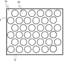
- FIG. 3 shows an aspect of the uneven portion provided on the crystal growth surface of the crystal substrate in the present invention.
- the uneven portion of FIG. 3 is composed of the crystal substrate 1 and the mask layer 4.
- FIG. 4 shows the surface of the uneven portion shown in FIG. 3 as viewed from the zenith direction.
- the mask layer 4 is formed on the crystal growth surface of the crystal substrate 1 and has holes in a dot shape.
- the crystal substrate 1 is exposed from the dot holes of the mask layer 4, and the dot-shaped recesses 2b are formed in a triangular lattice shape.
- the circles of the dots are provided at regular intervals a.
- the period a is not particularly limited, but in the present invention, it is preferably 1 ⁇ m to 1 mm, and more preferably 5 ⁇ m to 300 ⁇ m.
- the period a refers to the distance between the ends of circles of adjacent dots.
- the mask layer 4 can be formed by forming a film of the constituent material of the mask layer 4 and then processing it into a predetermined shape using a known means such as photolithography.
- the constituent material of the mask layer 4 include oxides such as Si, Ge, Ti, Zr, Hf, Ta, Sn, and Al, nitrides or carbides, carbon, diamond, metal, or a mixture thereof. Can be mentioned.
- the mask layer 4 preferably contains a metal oxide of a transition metal, more preferably contains a metal oxide of a Group 4 metal of the Periodic Table, and most preferably contains titanium oxide.
- the film forming means of the mask layer 4 is not particularly limited, and may be a known means. Examples of the means for forming the film of the constituent material of the mask layer 4 include a vacuum vapor deposition method, a CVD method, a sputtering method, and the like.
- the mask layer contains titanium oxide
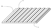
- FIG. 5 shows one aspect of the uneven portion provided on the crystal growth surface of the crystal substrate in the present invention.
- the uneven portion of FIG. 5 is composed of a crystal substrate 1 and a mask layer 4.
- the mask layer is formed in stripes on the crystal growth surface of the crystal substrate 1, and the recesses (grooves) 2b are formed in stripes by the mask layer 4.
- the mask layer 4 can be formed by using a known means such as photolithography.
- Examples of the constituent material of the mask layer 4 include oxides such as Si, Ge, Ti, Zr, Hf, Ta, Sn, and Al, nitrides or carbides, carbon, diamond, metal, or a mixture thereof. Can be mentioned.
- the mask layer 4 preferably contains a metal oxide of a transition metal, more preferably contains a metal oxide of a Group 4 metal of the Periodic Table, and most preferably contains titanium oxide.
- the constituent material of the mask layer such preferable, the crystallinity of the second crystal layer can be made more excellent.
- the width and height of the convex portion (mask layer) of the uneven portion, the width and depth of the concave portion, the interval, and the like are not particularly limited, but in the present invention, the width of the convex portion (mask layer) is about 1 ⁇ m to about 1 mm. It is preferably about 5 ⁇ m to about 300 ⁇ m, more preferably about 10 ⁇ m to about 100 ⁇ m.
- the height of the convex portion is preferably about 1 nm to about 10 ⁇ m, more preferably about 5 nm to about 1 ⁇ m, and more preferably about 10 nm to about 100 nm. Is the most preferable.
- the width of the recess is preferably about 1 ⁇ m to about 300 ⁇ m, more preferably about 3 ⁇ m to about 100 ⁇ m, and most preferably about 5 ⁇ m to about 50 ⁇ m.
- the depth of the recess is preferably about 1 nm to about 1 mm, more preferably about 10 nm to about 300 ⁇ m, and most preferably about 20 nm to about 100 ⁇ m.
- FIG. 2 shows a cross-sectional view of the crystalline laminated structure of the present invention.
- the first crystal layer 3 is formed on the crystal substrate 1, and the second crystal layer 5 is further formed by crystal growth.
- the first crystal layer 3 is provided with polycrystals 3a and single crystals 3b alternately adjacent to each other in the lateral direction.
- crystalline oxides are also grown laterally on the first crystal layer 3. In this way, by growing the second crystal layer 5 containing the single crystal of the crystalline oxide on the first crystal layer 3 containing polycrystals, the crystallinity of the second crystal layer 5 is further improved. Can be. Further, in the crystalline laminated structure of FIG.
- the polycrystals 3a and the single crystals 3b in the first crystal layer 3 are provided on the surface of the first crystal layer 3 and are alternately adjacent to each other in the lateral direction. Since it is provided, the second crystal layer 5 can be a high-quality crystal layer in which a well-continuous lateral growth portion is formed.
- a buffer layer including a stress relaxation layer or the like may be provided on the crystal substrate, and when the buffer layer is provided, the uneven portion may be formed on the buffer layer as well.
- the buffer layer may have crystallinity or may be amorphous, but it is preferable that the buffer layer has crystallinity.
- the buffer layer may be a single crystal layer or a polycrystalline layer. Further, the buffer layer may contain mixed crystals.
- the substrate has a buffer layer on a part or all of the surface.
- the means for forming the buffer layer is not particularly limited and may be a known means.
- the forming means include a spray method, a mist CVD method, an HVPE method, an MBE method, a MOCVD method, a sputtering method and the like.
- the buffer layer formed by the mist CVD method can improve the film quality of the crystal film formed on the buffer layer, and in particular, can cause crystal defects such as tilt. It is preferable because it can be suppressed.
- the means for forming the first crystal layer and the second crystal layer is not particularly limited and may be known means.
- the forming means include a CVD method, a MOCVD method, a MOVPE method, a mist CVD method, a mist epitaxy method, an MBE method, an HVPE method, a pulse growth method, an ALD method, a sputtering method and the like.
- the forming means is preferably a mist CVD method, a mist epitaxy method or an HVPE method, and more preferably an HVPE method.
- the means for forming the first crystal layer and the second crystal layer are the same, so that the first crystal layer and the second crystal layer can be continuously and efficiently formed. Therefore, it is preferable.
- the means for forming the stress relaxation layer and / or the crystalline oxide layer may be the same as the means for forming the first crystal layer and the second crystal layer.
- the present invention will be described in more detail by taking as an example the case where the HVPE method is used as a means for forming the first crystal layer or the second crystal layer (hereinafter, collectively referred to as “crystal layer”).
- a metal source containing a metal is gasified to obtain a metal halide gas, and then the metal halide gas and an oxygen-containing raw material gas are supplied to the crystal substrate in the reaction chamber. It is preferable that the reactive gas is supplied onto the crystal substrate and the film formation is carried out under the flow of the reactive gas.
- the metal source is not particularly limited as long as it contains a metal and can be gasified, and may be a simple substance of a metal or a metal compound.
- the metal include one or more metals selected from gallium, aluminum, indium, iron, chromium, vanadium, titanium, rhodium, nickel, cobalt, iridium and the like.
- the metal is preferably one or more metals selected from gallium, aluminum and indium, more preferably gallium, and the metal source is gallium alone. Most preferred.
- the metal source may be a gas, a liquid, or a solid, but in the present invention, for example, when gallium is used as the metal, the metal is used.
- the source is preferably a liquid.
- the gasification means is not particularly limited and may be a known means as long as the object of the present invention is not impaired.
- the gasification means is preferably carried out by halogenating the metal source.
- the halogenating agent used for the halogenation is not particularly limited as long as the metal source can be halogenated, and may be a known halogenating agent.
- the halogenating agent include halogens and hydrogen halides.
- the halogen include fluorine, chlorine, bromine, iodine and the like.
- hydrogen halide include hydrogen fluoride, hydrogen chloride, hydrogen bromide, hydrogen iodide and the like.
- the gasification is carried out by supplying halogen or hydrogen halide as a halogenating agent to the metal source and reacting the metal source with halogen or hydrogen halide at a temperature equal to or higher than the vaporization temperature of the metal halide. It is preferable to carry out the process by forming a metal halide.
- the halogenation reaction temperature is not particularly limited, but in the present invention, for example, when the metal source is gallium and the halogenating agent is HCl, 900 ° C. or lower is preferable, and 700 ° C. or lower is preferable.
- the metal halide gas is not particularly limited as long as it is a gas containing a halide of the metal of the metal source.
- the metal halide gas include halides of the metal (fluoride, chloride, bromide, iodide, etc.).
- the metal halide gas and the oxygen-containing raw material gas are supplied onto a substrate in the reaction chamber. Further, in the present invention, the reactive gas is supplied onto the substrate.
- the formation temperature of the crystal layer is not particularly limited, but in the present invention, for example, when the metal source is gallium and the halogenating agent is HCl, the temperature is preferably 900 ° C. or lower, preferably 700 ° C. or lower. Is more preferable, and the temperature is most preferably 400 ° C. to 700 ° C.
- the first crystal layer is formed at a low temperature (for example, less than 500 ° C.) and the second crystal layer is formed at a high temperature (for example, 500 ° C. or higher). It is preferable because the crystal layer and the second crystal layer can be made separately.
- the oxygen-containing raw material gas may be, for example, one or more gases selected from O 2 gas, CO 2 gas, NO gas, NO 2 gas, N 2 O gas, H 2 O gas or O 3 gas. is there.
- the reactive gas is usually a reactive gas different from the metal halide gas and the oxygen-containing raw material gas, and does not include an inert gas.
- the reactive gas is not particularly limited, and examples thereof include an etching gas and the like.
- the etching gas is not particularly limited and may be a known etching gas as long as the object of the present invention is not impaired.
- the reactive gas is a halogen gas (for example, fluorine gas, chlorine gas, bromine gas, iodine gas, etc.), hydrogen halide gas (for example, hydrofluoric acid gas, hydrochloric acid gas, hydrogen bromide gas, or hydrogen bromide gas).
- the metal halide gas, the oxygen-containing raw material gas, and the reactive gas may contain a carrier gas.
- the carrier gas include an inert gas such as nitrogen and argon.
- the partial pressure of the metal halide gas is not particularly limited, but in the present invention, it is preferably 0.5 Pa to 1 kPa, and more preferably 5 Pa to 0.5 kPa.
- the partial pressure of the oxygen-containing raw material gas is not particularly limited, but in the present invention, it is preferably 0.5 to 100 times the partial pressure of the metal halide gas, and 1 to 20 times the partial pressure. Is more preferable.
- the partial pressure of the reactive gas is also not particularly limited, but in the present invention, it is preferably 0.1 to 5 times, preferably 0.2 to 3 times, the partial pressure of the metal halide gas. Is more preferable.
- the dopant-containing raw material gas is not particularly limited as long as it contains a dopant.
- the dopant is also not particularly limited, but in the present invention, the dopant preferably contains one or more elements selected from germanium, silicon, titanium, zirconium, vanadium, niobium and tin, preferably germanium. It is more preferably containing silicon or tin, and most preferably it contains germanium.
- the dopant-containing raw material gas preferably has the dopant in the form of a compound (for example, a halide, an oxide, etc.), and more preferably in the form of a halide.
- the partial pressure of the dopant-containing raw material gas is not particularly limited, but in the present invention, it is preferably 1 ⁇ 10 -7 times to 0.1 times the partial pressure of the metal-containing raw material gas, and is 2.5 ⁇ . More preferably, it is 10-6 times to 7.5 ⁇ 10-2 times. In the present invention, it is preferable to supply the dopant-containing raw material gas together with the reactive gas onto the substrate.
- the stress relaxation layer is not particularly limited as long as it contains a polycrystal containing an oxide represented by M 2 O 3 (in the formula, M represents a trivalent metal atom and O represents an oxygen atom).
- M represents a trivalent metal atom
- O represents an oxygen atom
- the trivalent metal atom include aluminum (Al), gallium (Ga), indium (In), thallium (Tl), cobalt (Co), rhodium (Rh), iridium (Ir), and iron (Fe).
- the trivalent metal atom preferably contains a Group 13 metal of the Periodic Table, and more preferably gallium.
- the "main component” means, for example, when the polycrystal contains Ga 2 O 3 as a main component, the atomic ratio of gallium in the metal element in the polycrystal is 0.5 or more, and Ga 2 is used. If O 3 is included, that is sufficient.
- the atomic ratio of gallium in the metal element in the polycrystal is preferably 0.7 or more, more preferably 0.8 or more.
- the polycrystal may contain a mixed crystal, in which case, for example, the polycrystal may contain gallium and aluminum, indium, iron, chromium, vanadium, titanium, rhodium, nickel, cobalt and It preferably contains one or more metals selected from iridium.
- the crystal structure of the polycrystal is not particularly limited as long as the object of the present invention is not impaired.
- the crystal structure of the polycrystal includes, for example, a corundum structure, a ⁇ -gallia structure, a hexagonal structure (for example, ⁇ -type structure, etc.), a rectangular structure (for example, a ⁇ -type structure, etc.), a cubic structure, or a tetragonal crystal.
- the polycrystal preferably has a corundum structure, a ⁇ -Galia structure, a hexagonal structure (for example, ⁇ -type structure, etc.) or an orthorhombic structure (for example, ⁇ -type structure, etc.). It is more preferable to have (for example, a ⁇ type structure).
- the stress relaxation layer further contains a single crystal because the crystalline oxide layer formed on the stress relaxation layer can have higher quality.
- the constituent material of the single crystal is also not particularly limited as long as the object of the present invention is not impaired.
- the constituent material of the single crystal for example, a single metal oxide containing one or more metals selected from aluminum, gallium, indium, iron, chromium, vanadium, titanium, rhodium, nickel, cobalt and iridium.
- the single crystal preferably contains a single crystal of a metal oxide of at least one metal selected from aluminum, indium and gallium, and at least a single crystal of a metal oxide of a metal containing gallium. Is more preferable, and it is most preferable to contain single crystal gallium oxide or a mixed crystal thereof.
- the crystal structure of the single crystal is not particularly limited as long as the object of the present invention is not impaired.
- the crystal structure of the single crystal includes, for example, a corundum structure, a ⁇ -gallia structure, a hexagonal structure (for example, ⁇ -type structure, etc.), a rectangular structure (for example, a ⁇ -type structure, etc.), a cubic structure, or a tetragonal structure. And so on.
- the single crystal preferably has a corundum structure, a ⁇ -Galia structure hexagonal structure (for example, ⁇ -type structure, etc.) or an orthorhombic structure (for example, ⁇ -type structure, etc.), and has a corundum structure. Is more preferable.
- the thickness of the stress relaxation layer is not particularly limited and may be 1 ⁇ m or more or 1 ⁇ m or less.
- the stress relaxation layer may include an amorphous portion. Further, in the embodiment of the present invention, it is preferable that the stress relaxation layer has voids because the crystalline oxide layer can be made of higher quality.
- the stress relaxation layer of such a preferable embodiment can be obtained by appropriately adjusting conditions such as growth rate in the method of forming the stress relaxation layer.
- the polycrystal and the single crystal in the stress relaxation layer are provided adjacent to each other in the lateral direction, so that the lateral growth portion is better formed in the crystalline oxide layer. Therefore, it is preferable that they are provided alternately adjacent to each other in the lateral direction, and it is most preferable that the polycrystal and the single crystal are provided at least on the surface of the stress relaxation layer.
- the planar shape of the single crystal and / or the polycrystal is also not particularly limited, but in the present invention, it may be striped, island-shaped, rectangular or lattice-shaped (square lattice, oblique lattice, triangular lattice, hexagonal lattice). It is preferably present, more preferably striped or grid-like, and most preferably grid-like.
- the stress relaxation layer having a concave-convex portion or a convex portion formed on at least a part of the surface thereof is laminated as the stress relaxation layer to further improve the quality of the crystalline oxide layer. It is preferable because it can be used.
- Such a stress relaxation layer is formed, for example, by forming the uneven portion on the surface of the crystal substrate and then forming the stress relaxation layer on the uneven portion by using the above-mentioned preferable forming means. It can be preferably performed.
- the shape of the concavo-convex portion of the stress relaxation layer may be the same as the shape of the concavo-convex portion on the crystal substrate described above.
- the crystalline oxide layer is not particularly limited as long as it contains a single crystal of the crystalline oxide, but in the present invention, it is preferable to contain the single crystal of the crystalline oxide as a main component.
- the crystalline oxide may be a semiconductor.
- the crystalline oxide include crystals of a metal oxide containing one or more metals selected from aluminum, gallium, indium, iron, chromium, vanadium, titanium, rhodium, nickel, cobalt and iridium. Can be mentioned.
- the crystalline oxide preferably contains at least one metal selected from aluminum, indium and gallium, more preferably at least gallium, in crystalline gallium oxide or a mixed crystal thereof. Most preferably.
- the crystal structure of the crystalline oxide is not particularly limited.
- the crystal structure of the crystalline oxide includes, for example, a corundum structure, a ⁇ -gallia structure, a hexagonal structure (for example, ⁇ -type structure, etc.), an orthorhombic structure (for example, a ⁇ -type structure, etc.), a cubic structure, or a tetragonal structure.
- a crystal structure and the like can be mentioned.
- the crystalline oxide preferably has a corundum structure, a ⁇ -gaul structure or a hexagonal crystal (for example, an ⁇ -type structure), and more preferably has a corundum structure.
- the quality such as crystallinity of the crystalline oxide layer can be made more excellent.
- the "main component” is preferably 50% or more, more preferably 70% or more, still more preferably 90%, based on the atomic ratio of the crystalline oxide with respect to all the components of the crystalline oxide layer. It means that the above is included, and it means that it may be 100%.
- the thickness of the crystalline oxide layer is not particularly limited, but is preferably 10 ⁇ m or more, more preferably 30 ⁇ m or more, and most preferably 50 ⁇ m or more. Further, in the present invention, it is preferable that the crystalline oxide layer includes a lateral growth portion.
- the lateral growth portion is not particularly limited as long as it is a portion that grows in the lateral direction or substantially lateral direction with respect to the thickness direction of the crystalline oxide layer.
- the stress relaxation layer contains a single crystal
- the crystal structure of the crystalline oxide and the crystal structure of the single crystal in the stress relaxation layer are the same, that is, the crystallinity oxidation. Since the crystallinity of the laterally growing portion of the material layer can be made more excellent, it is preferable that the crystalline oxide and the constituent material of the single crystal in the stress relaxation layer are the same. preferable.
- the crystalline oxide layer may contain a dopant.
- the dopant is not particularly limited and may be a known one, and may be an n-type dopant or a p-type dopant.
- Examples of the n-type dopant include tin, germanium, silicon, titanium, zirconium, vanadium, niobium, two or more of these elements, and the like.
- Examples of the p-type dopant include Mg, H, Li, Na, K, Rb, Cs, Fr, Be, Ca, Sr, Ba, Ra, Mn, Fe, Co, Ni, Pd, Cu, Ag and Au. , Zn, Cd, Hg, Ti, Pb, N, P or two or more of these elements.
- the content of the dopant is also not particularly limited, but is preferably 0.00001 atomic% or more, more preferably 0.00001 atomic% to 20 atomic%, and 0. Most preferably, it is 0.001 atomic% to 10 atomic%.
- the crystalline laminated structure of the present invention can be particularly suitably used for semiconductor devices, and is particularly useful for power devices.
- Semiconductor devices formed using the crystalline laminated structure include transistors and TFTs such as MIS, HEMT, and MOS, Schottky barrier diodes using semiconductor-metal junctions, and PN or PIN combined with other P layers. Examples include diodes and light emitting / receiving elements.
- the crystalline laminated structure may be used as it is in a semiconductor device or the like, or the crystal substrate and / or the first crystal layer and the second crystal layer may be peeled off by a known means. It may be applied to a semiconductor device or the like.
- the semiconductor device of the present invention is suitably used as a power module, an inverter or a converter by using known means, and these semiconductor devices are also included in the present invention. Further, the semiconductor device of the present invention is further preferably used for, for example, a semiconductor system using a power supply device.
- the power supply device can be manufactured from or as the semiconductor device by connecting to a wiring pattern or the like using a known means.
- FIG. 10 shows an example of a power supply system.
- a power supply system is configured by using the plurality of power supply devices and control circuits. As shown in FIG. 11, the power supply system can be used in a system device in combination with an electronic circuit.
- An example of the power supply circuit diagram of the power supply device is shown in FIG. FIG.
- a DC voltage is switched at a high frequency by an inverter (MOSFET: composed of A to D), converted to AC, and then insulated and transformed by a transformer. This is performed, rectified by a rectifying MOSFET (A to B'), smoothed by a DCL (smoothing coils L1 and L2) and a capacitor, and a DC voltage is output. At this time, the output voltage is compared with the reference voltage by the voltage comparator, and the inverter and the rectifying MOSFET are controlled by the PWM control circuit so as to obtain the desired output voltage.
- MOSFET composed of A to D
- Example 1 Mask formation A sapphire substrate (c-plane, off-angle 0.25 °) having an ⁇ -Ga 2 O 3 layer formed on its surface is used as the substrate, and a mask layer made of titanium oxide is used on the substrate by a sputtering method. Then, using a photolithography method, the formed mask layer was processed into a mask having a predetermined shape. In the sputtering method, a mask layer (thickness 50 nm) made of titanium oxide was formed by using a Ti target while flowing O 2 gas.
- the openings (dots) are arranged on the substrate in a triangular lattice pattern with a period (distance between the ends of adjacent dots) of 20 ⁇ m.
- the mask layer was processed.
- the halide vapor deposition (HVPE) device 50 used in this embodiment will be described with reference to FIG.
- the HVPE apparatus 50 includes a reaction chamber 51, a heater 52a for heating the metal source 57, and a heater 52b for heating the substrate fixed to the substrate holder 56, and further supplies an oxygen-containing raw material gas into the reaction chamber 51. It includes a pipe 55b, a reactive gas supply pipe 54b, and a board holder 56 on which a board is installed.
- a metal-containing raw material gas (metal halide gas) supply pipe 53b is provided in the reactive gas supply pipe 54b to form a double pipe structure.
- the oxygen-containing raw material gas supply pipe 55b is connected to the oxygen-containing raw material gas supply source 55a, and the oxygen-containing raw material gas is transferred from the oxygen-containing raw material gas supply source 55a via the oxygen-containing raw material gas supply pipe 55b to the substrate holder.
- the flow path of the oxygen-containing raw material gas is configured so that it can be supplied to the substrate fixed to 56.
- the reactive gas supply pipe 54b is connected to the reactive gas supply source 54a, and the reactive gas is fixed to the substrate holder 56 from the reactive gas supply source 54a via the reactive gas supply pipe 54b.
- the flow path of the reactive gas is configured so that it can be supplied to the substrate.
- the metal-containing raw material gas supply pipe 53b is connected to the halogen-containing raw material gas supply source 53a, and the halogen-containing raw material gas is supplied to the metal source to become the metal-containing raw material gas, and the metal-containing raw material gas is fixed to the substrate holder 56. It is supplied to the substrate.
- the reaction chamber 51 is provided with a gas discharge unit 59 for exhausting used gas, and further, a protective sheet 58 for preventing precipitation of reactants is provided on the inner wall of the reaction chamber 51.
- a gallium (Ga) metal source 57 (purity 99.99999% or more) is arranged inside the metal-containing raw material gas supply pipe 53b, and the above 1.
- the sapphire substrate with the mask layer obtained in the above was installed.
- the heaters 52a and 52b were operated to raise the temperature in the reaction chamber 51 to 570 ° C (near the Ga metal source) and 540 ° C (near the substrate holder).
- Hydrogen chloride (HCl) gas (purity 99.999% or more) was supplied from the halogen-containing raw material gas supply source 53a to the gallium (Ga) metal 57 arranged inside the film-forming metal raw material-containing gas supply pipe 53b.
- Gallium chloride (GaCl / GaCl 3 ) was produced by a chemical reaction between a Ga metal and hydrogen chloride (HCl) gas.
- the obtained gallium chloride (GaCl / GaCl 3 ) and O 2 gas (purity 99.99995% or more) supplied from the oxygen-containing raw material gas supply source 55a are supplied onto the substrate through the reactive gas supply pipe 54b. did.
- the flow rate of the HCl gas supplied from the halogen-containing raw material gas supply source 53a is 10 sccm
- the flow rate of the HCl gas supplied from the reactive gas supply source 54a is 10 sccm
- the flow rate of the HCl gas supplied from the oxygen-containing raw material gas supply source 55a is O.
- the flow rates of the two gases were maintained at 100 sccm, respectively.
- FIGS. 6 and 7 show an SEM image of the laminated structure after 60 minutes of film formation
- FIG. 7 shows an SEM image of the laminated structure after 120 minutes of film formation
- 7 (a) shows a bird's-eye view
- FIG. 7 (b) shows a cross-sectional view. From the SEM observation results of FIGS. 6 and 7 and the analysis results using the XRD diffractometer, polycrystals containing k-Ga 2 O 3 and ⁇ -Ga 2 O 3 single crystals are alternately adjacent to each other on a mask made of titanium oxide.
- the ⁇ -Ga 2 O 3 single crystal (second crystal) was grown in the vertical direction and the horizontal direction. Further, even when the film was formed for a long time, the crystal film did not peel off from the substrate, and a high-quality ⁇ -Ga 2 O 3 single crystal was formed. Further, when the film formation was further continued on the laminated structure shown in FIG. 7, the lateral growth portions were associated with each other, and a high-quality single crystal layer (second crystal layer) having a continuous lateral growth portion was formed. Was found to be formed.
- Example 1 A laminated structure was produced in the same manner as in Example 1 except that SiO 2 was used as the mask material. The obtained laminated structure was observed by SEM. The results are shown in FIG. From the SEM observation result of FIG. 8 and the analysis result using the XRD diffractometer , an amorphous portion was formed on the SiO 2 mask, and a part of the amorphous portion grew abnormally and ⁇ -Ga 2 O. It was found that 3 was formed.
- Example 2 In the formation of the titanium oxide mask layer by the sputtering method, a laminated structure was produced in the same manner as in Example 1 except that the thickness of the titanium oxide layer was set to 10 nm. The obtained laminated structure was observed by SEM.
- the SEM image of the laminated structure after the film formation is shown in FIG. 9 (a) shows a bird's-eye view, and FIG. 9 (b) shows a cross-sectional view. From the SEM observation result of FIG. 9 and the analysis result using the XRD diffractometer, a ⁇ -Ga 2 O 3 single crystal layer was formed on the titanium oxide mask, and an ⁇ -Ga 2 O 3 layer was formed on the single crystal layer. It was found that (second crystal layer) was formed. Further, with respect to the laminated structure shown in FIG. 9, when the film formation was continued for 120 minutes and then the film formation was continued, the crystal layer was peeled off from the substrate and the film could not be further thickened.
- Comparative Example 3 A laminated structure was produced in the same manner as in Example 1 except that an alumina (Al 2 O 3 ) mask layer was used instead of the titanium oxide mask layer. As a result, as in the case of Comparative Example 1, an amorphous portion is formed on the mask and abnormal growth occurs, and if the growth is continued, the crystal layer is peeled off from the substrate and the film cannot be thickened. It was.
- an alumina (Al 2 O 3 ) mask layer was used instead of the titanium oxide mask layer.
- Example 2 A laminated structure was obtained in the same manner as in Example 1 except that the first crystal layer was formed so that the mask width was 10 ⁇ m and at least a part of the first crystal layer had voids. It was. More specifically, by first growing at a growth temperature of 520 ° C. for 20 minutes, then lowering the growth temperature to 460 ° C. and growing for another 40 minutes, the polycrystalline k-Ga 2 O 3 having a void structure is masked. Accumulated on top. The obtained laminated structure was observed by SEM. The results are shown in FIG. From the SEM observation result of FIG.
- the crystalline laminated structure and semiconductor device of the present invention can be used in all fields such as semiconductors (for example, compound semiconductor electronic devices, etc.), electronic parts / electrical equipment parts, optical / electrophotographic-related equipment, industrial parts, etc. , Useful for manufacturing semiconductor devices and the like.
- semiconductors for example, compound semiconductor electronic devices, etc.
- electronic parts / electrical equipment parts for example, electronic parts / electrical equipment parts
- optical / electrophotographic-related equipment for manufacturing semiconductor devices and the like.
Landscapes
- Chemical & Material Sciences (AREA)
- Engineering & Computer Science (AREA)
- Microelectronics & Electronic Packaging (AREA)
- Power Engineering (AREA)
- Crystallography & Structural Chemistry (AREA)
- Materials Engineering (AREA)
- Metallurgy (AREA)
- Organic Chemistry (AREA)
- Ceramic Engineering (AREA)
- General Chemical & Material Sciences (AREA)
- Condensed Matter Physics & Semiconductors (AREA)
- General Physics & Mathematics (AREA)
- Chemical Kinetics & Catalysis (AREA)
- Physics & Mathematics (AREA)
- Computer Hardware Design (AREA)
- Inorganic Chemistry (AREA)
- Chemical Vapour Deposition (AREA)
- Crystals, And After-Treatments Of Crystals (AREA)
Abstract
高品質な結晶層を備える結晶性積層構造体、およびこのような結晶性積層構造体を備える半導体装置を提供する。第1の結晶を含む第1の結晶層上に、第2の結晶を含む第2の結晶層が積層されている結晶性積層構造体であって、第1の結晶が、M2O3(式中、Mは3価の金属原子、Oは酸素原子を示す)で表される酸化物を含有する多結晶であり、第2の結晶が結晶性酸化物の単結晶である結晶性積層構造体を、半導体装置に適用する。
Description
本発明は、半導体装置の製造等に有用な結晶性積層構造体および半導体装置に関する。
高耐圧、低損失および高耐熱を実現できる次世代のスイッチング素子として、バンドギャップの大きな酸化ガリウム(Ga2O3)を用いた半導体装置が注目されており、インバータなどの電力用半導体装置への適用が期待されている。また、広いバンドギャップからLEDやセンサー等の受発光装置としての幅広い応用も期待されている。特に、酸化ガリウムの中でもコランダム構造を有するα―Ga2O3等は、インジウムやアルミニウムをそれぞれ、あるいは組み合わせて混晶することによりバンドギャップ制御することが可能であり、InAlGaO系半導体として極めて魅力的な材料系統を構成している。ここでInAlGaO系半導体とはInXAlYGaZO3(0≦X≦2、0≦Y≦2、0≦Z≦2、X+Y+Z=1.5~2.5)を示し(特許文献9等)、酸化ガリウムを内包する同一材料系統として俯瞰することができる。
しかしながら、酸化ガリウムは、最安定相がβガリア構造であるので、特殊な成膜法を用いなければ、準安定相であるコランダム構造の結晶膜を成膜することが困難である。また、コランダム構造を有するα―Ga2O3は準安定相であり、融液成長によるバルク基板が利用できない。そのため、現状はα―Ga2O3と同じ結晶構造を有するサファイアを基板として用いている。しかし、α―Ga2O3とサファイアとは格子不整合度が大きいため、サファイア基板上にヘテロエピタキシャル成長されるα―Ga2O3の結晶膜は、転位密度が高くなる傾向がある。また、コランダム構造の結晶膜に限らず、成膜レートや結晶品質の向上、クラックや異常成長の抑制、ツイン抑制、反りによる基板の割れ等においてもまだまだ課題が数多く存在している。このような状況下、現在、コランダム構造を有する結晶性半導体の成膜について、いくつか検討がなされている。
特許文献1には、ガリウム又はインジウムの臭化物又はヨウ化物を用いて、ミストCVD法により、酸化物結晶薄膜を製造する方法が記載されている。特許文献2~4には、コランダム型結晶構造を有する下地基板上に、コランダム型結晶構造を有する半導体層と、コランダム型結晶構造を有する絶縁膜とが積層された多層構造体が記載されている。また、特許文献5~7のように、ELO基板やボイド形成を用いて、ミストCVDによる成膜も検討されている。しかしながら、いずれの方法も結晶品質と大面積化との両立等においてまだまだ満足のいくものではなく、大面積且つ結晶品質に優れた結晶膜が待ち望まれていた。
特許文献8には、少なくとも、ガリウム原料と酸素原料とを用いて、ハライド気相成長法(HVPE法)により、コランダム構造を有する酸化ガリウムを成膜することが記載されている。また、非特許文献1には、HVPE法用いてELO基板上に酸化ガリウムを成膜することが記載されている。しかしながら、α―Ga2O3は準安定相であるので、β―Ga2O3のように成膜することが困難であり、工業的にはまだまだ多くの課題があった。
なお、特許文献1~8はいずれも本出願人らによる特許または特許出願に関する公報であり、現在も検討が進められている。
特許文献8には、少なくとも、ガリウム原料と酸素原料とを用いて、ハライド気相成長法(HVPE法)により、コランダム構造を有する酸化ガリウムを成膜することが記載されている。また、非特許文献1には、HVPE法用いてELO基板上に酸化ガリウムを成膜することが記載されている。しかしながら、α―Ga2O3は準安定相であるので、β―Ga2O3のように成膜することが困難であり、工業的にはまだまだ多くの課題があった。
なお、特許文献1~8はいずれも本出願人らによる特許または特許出願に関する公報であり、現在も検討が進められている。
Oshima, Y., et al. "Epitaxial lateral overgrowth of α-Ga2O3 by halide vapor phase epitaxy." APL Materials 7.2 (2019): 022503.
本発明は、高品質な結晶層を備える結晶性積層構造体およびこのような結晶性積層構造体を備える半導体装置を提供することを目的とする。
本発明者らは、上記目的を達成すべく鋭意検討した結果、第1の結晶を含む第1の結晶層上に、第2の結晶を含む第2の結晶層が積層されている結晶性積層構造体を製造する際に、第1の結晶として、M2O3(式中、Mは3価の金属原子、Oは酸素原子を示す)で表される酸化物を含有する多結晶を形成し、第2の結晶、結晶性酸化物の単結晶を形成すると、得られた結晶性積層構造体における第2の結晶層の結晶性等の品質が優れたものとなることを知見し、このような結晶性積層構造体によれば、上記した従来の問題を一挙に解決できることを見出した。
また、本発明者らは、上記知見を得た後、さらに検討を重ねて本発明を完成させるに至った。
すなわち、本発明は、以下の発明に関する。
[1] 第1の結晶を含む第1の結晶層上に、第2の結晶を含む第2の結晶層が積層されている結晶性積層構造体であって、第1の結晶が、M2O3(式中、Mは3価の金属原子、Oは酸素原子を示す)で表される酸化物を含有する多結晶であり、第2の結晶が結晶性酸化物の単結晶であることを特徴とする結晶性積層構造体。
[2] 3価の金属原子が、周期律表第13族金属を含む前記[1]記載の結晶性積層構造体。
[3] 3価の金属原子が、ガリウムを含む前記[1]または[2]に記載の結晶性積層構造体。
[4] 第1の結晶層が、さらに単結晶を含むことを特徴とする前記[1]~[3]のいずれかに記載の結晶性積層構造体。
[5] 前記多結晶および前記単結晶が、横方向に隣接して設けられている前記[4]記載の結晶性積層構造体。
[6] 少なくとも第1の結晶層の表面に前記多結晶および前記単結晶が設けられている前記[5]記載の結晶性積層構造体。
[7] 第2の結晶層が、横方向成長部を含む前記[1]~[6]のいずれかに記載の結晶性積層構造体。
[8] 前記結晶性酸化物が、アルミニウム、インジウムおよびガリウムから選ばれる少なくとも1種の金属を含む前記[1]~[7]のいずれかに記載の結晶性積層構造体。
[9] 前記結晶性酸化物が少なくともガリウムを含む前記[1]~[8]のいずれかに記載の結晶性積層構造体。
[10] 前記結晶性酸化物がコランダム構造を有する前記[1]~[9]のいずれかに記載の結晶性積層構造体。
[11] 結晶基板上に、第1の結晶を含む第1の結晶層を介して、第2の結晶を含む第2の結晶層が積層されている結晶性積層構造体であって、第1の結晶がM2O3(式中、Mは3価の金属原子、Oは酸素原子を示す)で表される酸化物を含有する多結晶であり、第2の結晶が結晶性酸化物の単結晶であることを特徴とする結晶性積層構造体。
[12] 前記結晶基板上に、マスク層を介して、第1の結晶層が積層されている前記[11]記載の結晶性積層構造体。
[13] 前記[1]~[12]のいずれかに記載の結晶性積層構造体を用いてなる半導体装置。
[14] 半導体装置を備える半導体システムであって、前記半導体装置が、前記[13]記載の半導体装置であることを特徴とする半導体システム。
[15] 結晶基板上に、応力緩和層を介して、結晶性酸化物の単結晶を含む結晶性酸化物層を形成する結晶性積層構造体の製造方法であって、前記応力緩和層に、M2O3(式中、Mは3価の金属原子、Oは酸素原子を示す)で表される酸化物を含有する多結晶を用いることを特徴とする結晶性積層構造体の製造方法。
[16] 3価の金属原子が、周期律表第13族金属を含む前記[15]記載の製造方法。
[17] 3価の金属原子が、ガリウムを含む前記[15]または[16]に記載の製造方法。
[18] 前記応力緩和層が、さらに単結晶を含む前記[15]~[17]のいずれかに記載の製造方法。
[19] 前記多結晶および前記単結晶が横方向に隣接して設けられている前記[18]記載の製造方法。
[20] 少なくとも前記応力緩和層の表面に前記多結晶および前記単結晶が設けられている前記[19]記載の製造方法。
[21] 前記結晶基板が、サファイア基板である前記[15]~[20]のいずれかに記載の製造方法。
[22] 前記応力緩和層が、表面の少なくとも一部に凹部または凸部からなる凹凸部を有する前記[15]~[21]のいずれかに記載の製造方法。
[23] 前記応力緩和層の形成を、前記結晶基板上に、直接または他の層を介して、凹部または凸部からなる凹凸部を形成し、ついで、該凹凸部上に、前記応力緩和層を成膜することにより行う前記[15]~[22]のいずれかに記載の製造方法。
[24] 前記凹凸部の形成を、前記結晶基板上に直接または他の層を介してマスクを規則的に配列することにより行う前記[23]記載の製造方法。
[25] 前記多結晶を少なくとも前記マスク上に形成する前記[24]記載の製造方法。
[26] 前記マスク層が、周期律表第4族金属の金属酸化物を含む前記[24]または[25]に記載の製造方法。
[27] 周期律表第4族金属が、チタン、ジルコニウムまたはハフニウムである前記[26]記載の製造方法。
本発明の結晶性積層構造体は、高品質な結晶層を備えている。
本発明の結晶性積層構造体は、第1の結晶を含む第1の結晶層上に、第2の結晶を含む第2の結晶層が積層されている結晶性積層構造体であって、第1の結晶が、M2O3(式中、Mは3価の金属原子、Oは酸素原子を示す)で表される酸化物を含有する多結晶であり、第2の結晶が結晶性酸化物の単結晶であることを特長とする。本発明においては、第2の結晶層の少なくとも一部が第1の結晶層に接触するように第2の結晶層が積層されているのが好ましい。ここで、「単結晶」とは、結晶面、結晶軸が揃っている単一の結晶子からなる結晶をいう。また、「多結晶」とは、結晶面、結晶軸が異なる2以上の結晶子が粒界を介して接合または集積してなる結晶をいう。
(第1の結晶層)
第1の結晶は、M2O3(式中、Mは3価の金属原子、Oは酸素原子を示す)で表される酸化物を含有する多結晶であれば、特に限定されない。本発明においては、前記多結晶が、M2O3(式中、Mは3価の金属原子、Oは酸素原子を示す)で表される酸化物を主成分として含むのが好ましい。前記3価の金属原子としては、例えば、アルミニウム(Al)、ガリウム(Ga)、インジウム(In)、タリウム(Tl)、コバルト(Co)、ロジウム(Rh)、イリジウム(Ir)、鉄(Fe)、マンガン(Mn)、クロム(Cr)およびバナジウム(V)から選ばれる1種または2種以上の金属等が挙げられる。本発明においては、前記3価の金属原子が、周期律表第13族金属を含むのが好ましく、ガリウムを含むのがより好ましい。ここで、「主成分」とは、例えば、前記多結晶がGa2O3を主成分として含む場合、前記多結晶中の金属元素中のガリウムの原子比が0.5以上の割合でGa2O3が含まれていればそれでよい。本発明においては、前記多結晶中の金属元素中のガリウムの原子比が0.7以上であるのが好ましく、0.8以上であるのがより好ましい。本発明においては、前記多結晶が、混晶を含んでいてもよく、この場合、例えば、前記多結晶が、ガリウムと、アルミニウム、インジウム、鉄、クロム、バナジウム、チタン、ロジウム、ニッケル、コバルトおよびイリジウムから選ばれる1種または2種以上の金属とを含むのが好ましい。なお、前記多結晶が有する結晶構造は、本発明の目的を阻害しない限り、特に限定されない。前記多結晶が有する結晶構造としては、例えば、コランダム構造、β―ガリア構造、六方晶構造(例えば、ε型構造等)、直方晶構造(例えばκ型構造等)、立方晶構造、または正方晶構造等が挙げられる。本発明においては、前記多結晶が、コランダム構造、β―ガリア構造、六方晶構造(例えば、ε型構造等)または直方晶構造(例えばκ型構造等)を有するのが好ましく、直方晶構造(例えばκ型構造等)を有するのがより好ましい。また、本発明においては、第1の結晶層が、さらに単結晶を含むのが、第2の結晶層をより高品質なものとすることができるので、好ましい。前記単結晶の構成材料も、本発明の目的を阻害しない限り、特に限定されない。前記単結晶の構成材料としては、例えば、アルミニウム、ガリウム、インジウム、鉄、クロム、バナジウム、チタン、ロジウム、ニッケル、コバルトおよびイリジウムから選ばれる1種または2種以上の金属を含む金属酸化物の単結晶などが挙げられる。また、本発明においては、前記単結晶が、アルミニウム、インジウムおよびガリウムから選ばれる少なくとも1種の金属の金属酸化物の単結晶を含むのが好ましく、少なくともガリウムを含む金属の金属酸化物の単結晶を含むのがより好ましく、単結晶酸化ガリウムまたはその混晶を含むのが最も好ましい。また、前記単結晶の結晶構造は、本発明の目的を阻害しない限り、特に限定されない。前記単結晶の結晶構造としては、例えば、コランダム構造、β―ガリア構造、六方晶構造(例えば、ε型構造等)、直方晶構造(例えばκ型構造等)、立方晶構造、または正方晶構造等が挙げられる。本発明においては、前記単結晶が、コランダム構造、β―ガリア構造、六方晶構造(例えば、ε型構造等)または直方晶構造(例えばκ型構造等)を有するのが好ましく、コランダム構造を有するのがより好ましい。第1の結晶層の厚さは、特に限定されず、1μm以上であってもよいし、1μm以下であってもよい。なお、本発明においては、第1の結晶層が、非晶質部分を含んでいてもよい。また、本発明の実施態様においては、第1の結晶層が、空隙を有しているのも、第2の結晶層をより高品質なものとすることができるので、好ましい。このような好ましい態様の第1の結晶層は、後述する第1の結晶層の形成方法において、成長速度や成長温度等の条件を適宜調整することにより得ることができる。
第1の結晶は、M2O3(式中、Mは3価の金属原子、Oは酸素原子を示す)で表される酸化物を含有する多結晶であれば、特に限定されない。本発明においては、前記多結晶が、M2O3(式中、Mは3価の金属原子、Oは酸素原子を示す)で表される酸化物を主成分として含むのが好ましい。前記3価の金属原子としては、例えば、アルミニウム(Al)、ガリウム(Ga)、インジウム(In)、タリウム(Tl)、コバルト(Co)、ロジウム(Rh)、イリジウム(Ir)、鉄(Fe)、マンガン(Mn)、クロム(Cr)およびバナジウム(V)から選ばれる1種または2種以上の金属等が挙げられる。本発明においては、前記3価の金属原子が、周期律表第13族金属を含むのが好ましく、ガリウムを含むのがより好ましい。ここで、「主成分」とは、例えば、前記多結晶がGa2O3を主成分として含む場合、前記多結晶中の金属元素中のガリウムの原子比が0.5以上の割合でGa2O3が含まれていればそれでよい。本発明においては、前記多結晶中の金属元素中のガリウムの原子比が0.7以上であるのが好ましく、0.8以上であるのがより好ましい。本発明においては、前記多結晶が、混晶を含んでいてもよく、この場合、例えば、前記多結晶が、ガリウムと、アルミニウム、インジウム、鉄、クロム、バナジウム、チタン、ロジウム、ニッケル、コバルトおよびイリジウムから選ばれる1種または2種以上の金属とを含むのが好ましい。なお、前記多結晶が有する結晶構造は、本発明の目的を阻害しない限り、特に限定されない。前記多結晶が有する結晶構造としては、例えば、コランダム構造、β―ガリア構造、六方晶構造(例えば、ε型構造等)、直方晶構造(例えばκ型構造等)、立方晶構造、または正方晶構造等が挙げられる。本発明においては、前記多結晶が、コランダム構造、β―ガリア構造、六方晶構造(例えば、ε型構造等)または直方晶構造(例えばκ型構造等)を有するのが好ましく、直方晶構造(例えばκ型構造等)を有するのがより好ましい。また、本発明においては、第1の結晶層が、さらに単結晶を含むのが、第2の結晶層をより高品質なものとすることができるので、好ましい。前記単結晶の構成材料も、本発明の目的を阻害しない限り、特に限定されない。前記単結晶の構成材料としては、例えば、アルミニウム、ガリウム、インジウム、鉄、クロム、バナジウム、チタン、ロジウム、ニッケル、コバルトおよびイリジウムから選ばれる1種または2種以上の金属を含む金属酸化物の単結晶などが挙げられる。また、本発明においては、前記単結晶が、アルミニウム、インジウムおよびガリウムから選ばれる少なくとも1種の金属の金属酸化物の単結晶を含むのが好ましく、少なくともガリウムを含む金属の金属酸化物の単結晶を含むのがより好ましく、単結晶酸化ガリウムまたはその混晶を含むのが最も好ましい。また、前記単結晶の結晶構造は、本発明の目的を阻害しない限り、特に限定されない。前記単結晶の結晶構造としては、例えば、コランダム構造、β―ガリア構造、六方晶構造(例えば、ε型構造等)、直方晶構造(例えばκ型構造等)、立方晶構造、または正方晶構造等が挙げられる。本発明においては、前記単結晶が、コランダム構造、β―ガリア構造、六方晶構造(例えば、ε型構造等)または直方晶構造(例えばκ型構造等)を有するのが好ましく、コランダム構造を有するのがより好ましい。第1の結晶層の厚さは、特に限定されず、1μm以上であってもよいし、1μm以下であってもよい。なお、本発明においては、第1の結晶層が、非晶質部分を含んでいてもよい。また、本発明の実施態様においては、第1の結晶層が、空隙を有しているのも、第2の結晶層をより高品質なものとすることができるので、好ましい。このような好ましい態様の第1の結晶層は、後述する第1の結晶層の形成方法において、成長速度や成長温度等の条件を適宜調整することにより得ることができる。
本発明においては、第1の結晶層における前記多結晶と前記単結晶とが、横方向に隣接して設けられているのが、第2の結晶層において横方向成長部がより良好に形成されるので、好ましく、横方向に交互に隣接して設けられているのが、より好ましく、少なくとも第1の結晶層の表面に前記多結晶および前記単結晶が設けられているのが最も好ましい。前記単結晶および/または前記多結晶の平面形状も、特に限定されないが、本発明においては、ストライプ状、島状、矩形状または格子状(正方格子、斜方格子、三角格子、六角格子)であるのが好ましく、ストライプ状または格子状であるのがより好ましく、格子状であるのが最も好ましい。前記多結晶と前記単結晶とをこのような好ましい構成とすることにより、第2の結晶層の結晶性等の品質をより優れたものとすることができる。
(第2の結晶層)
第2の結晶は、結晶性酸化物の単結晶であれば、特に限定されない。第2の結晶層が、第2の結晶を主成分として含むのが好ましい。また、本発明においては、前記結晶性酸化物が半導体であってもよい。前記結晶性酸化物としては、例えば、アルミニウム、ガリウム、インジウム、鉄、クロム、バナジウム、チタン、ロジウム、ニッケル、コバルトおよびイリジウムから選ばれる1種または2種以上の金属を含む金属酸化物の結晶などが挙げられる。本発明においては、前記結晶性酸化物が、アルミニウム、インジウムおよびガリウムから選ばれる少なくとも1種の金属を含有するのが好ましく、少なくともガリウムを含むのがより好ましく、結晶性酸化ガリウムまたはその混晶であるのが最も好ましい。前記結晶性酸化物の結晶構造は、本発明の目的を阻害しない限り、特に限定されない。前記結晶性酸化物の結晶構造としては、例えば、コランダム構造、β―ガリア構造、六方晶構造(例えば、ε型構造等)、直方晶構造(例えばκ型構造等)、立方晶構造、または正方晶構造等が挙げられる。本発明においては、前記結晶性酸化物が、コランダム構造、β―ガリア構造または六方晶(例えば、ε型構造等)を有するのが好ましく、コランダム構造を有するのがより好ましい。このような好ましい第2の結晶層と上記した好ましい第1の結晶層とを組み合わせることにより、第2の結晶層の結晶性等の品質をより優れたものとすることができる。なお、「主成分」とは、第2の結晶が、原子比で、第2の結晶層の全成分に対し、好ましくは50%以上、より好ましくは70%以上、更に好ましくは90%以上含まれることを意味し、100%であってもよいことを意味する。第2の結晶層の厚さは、特に限定されないが、10μm以上であるのが好ましく、30μm以上であるのがより好ましく、50μm以上であるのが最も好ましい。また、本発明においては、第2の結晶層が、横方向成長部を含むのが好ましい。前記横方向成長部は、第2の結晶層の厚さ方向に対して横方向または略横方向に成長した部分であれば、特に限定されない。また、本発明においては、第1の結晶層が単結晶を含む場合、前記結晶性酸化物の結晶構造と第1の結晶層における前記単結晶の結晶構造とが同じであるのが、第2の結晶層の横方向成長部の品質をより優れたものとすることができるので、好ましく、前記結晶性酸化物と第1の結晶層における前記単結晶の構成材料とが同じであるのがより好ましい。
第2の結晶は、結晶性酸化物の単結晶であれば、特に限定されない。第2の結晶層が、第2の結晶を主成分として含むのが好ましい。また、本発明においては、前記結晶性酸化物が半導体であってもよい。前記結晶性酸化物としては、例えば、アルミニウム、ガリウム、インジウム、鉄、クロム、バナジウム、チタン、ロジウム、ニッケル、コバルトおよびイリジウムから選ばれる1種または2種以上の金属を含む金属酸化物の結晶などが挙げられる。本発明においては、前記結晶性酸化物が、アルミニウム、インジウムおよびガリウムから選ばれる少なくとも1種の金属を含有するのが好ましく、少なくともガリウムを含むのがより好ましく、結晶性酸化ガリウムまたはその混晶であるのが最も好ましい。前記結晶性酸化物の結晶構造は、本発明の目的を阻害しない限り、特に限定されない。前記結晶性酸化物の結晶構造としては、例えば、コランダム構造、β―ガリア構造、六方晶構造(例えば、ε型構造等)、直方晶構造(例えばκ型構造等)、立方晶構造、または正方晶構造等が挙げられる。本発明においては、前記結晶性酸化物が、コランダム構造、β―ガリア構造または六方晶(例えば、ε型構造等)を有するのが好ましく、コランダム構造を有するのがより好ましい。このような好ましい第2の結晶層と上記した好ましい第1の結晶層とを組み合わせることにより、第2の結晶層の結晶性等の品質をより優れたものとすることができる。なお、「主成分」とは、第2の結晶が、原子比で、第2の結晶層の全成分に対し、好ましくは50%以上、より好ましくは70%以上、更に好ましくは90%以上含まれることを意味し、100%であってもよいことを意味する。第2の結晶層の厚さは、特に限定されないが、10μm以上であるのが好ましく、30μm以上であるのがより好ましく、50μm以上であるのが最も好ましい。また、本発明においては、第2の結晶層が、横方向成長部を含むのが好ましい。前記横方向成長部は、第2の結晶層の厚さ方向に対して横方向または略横方向に成長した部分であれば、特に限定されない。また、本発明においては、第1の結晶層が単結晶を含む場合、前記結晶性酸化物の結晶構造と第1の結晶層における前記単結晶の結晶構造とが同じであるのが、第2の結晶層の横方向成長部の品質をより優れたものとすることができるので、好ましく、前記結晶性酸化物と第1の結晶層における前記単結晶の構成材料とが同じであるのがより好ましい。
第2の結晶層には、ドーパントが含まれていてもよい。前記ドーパントは、特に限定されず、公知のものであってよく、n型ドーパントであってもよいし、p型ドーパントであってもよい。前記n型ドーパントとしては、スズ、ゲルマニウム、ケイ素、チタン、ジルコニウム、バナジウム、ニオブまたはこれらの2種以上の元素等が挙げられる。前記p型ドーパントとしては、例えば、Mg、H、Li、Na、K、Rb、Cs、Fr、Be、Ca、Sr、Ba、Ra、Mn、Fe、Co、Ni、Pd、Cu、Ag、Au、Zn、Cd、Hg、Ti、Pb、N、Pまたはこれらの2種以上の元素等が挙げられる。前記ドーパントの含有量も、特に限定されないが、第2の結晶層中、0.00001原子%以上であるのが好ましく、0.00001原子%~20原子%であるのがより好ましく、0.00001原子%~10原子%であるのが最も好ましい。
前記結晶性積層構造体は、例えば、結晶基板上に第1の結晶層および第2の結晶層を形成して結晶性積層構造体を製造する方法において、前記結晶基板上に、M2O3(式中、Mは3価の金属原子、Oは酸素原子を示す)で表される酸化物を含有する多結晶を含む第1の結晶層を形成し、さらに、第1の結晶層上に、結晶性酸化物の単結晶を含む第2の結晶層を形成することにより、好適に得ることができる。第1の結晶層および第2の結晶層の形成は、公知の手段を用いて行うことができる。前記結晶性積層構造体は、より具体的には、例えば、結晶基板上に、応力緩和層を介して、結晶性酸化物の単結晶を含む結晶性酸化物層(以下、「第2の結晶層」ともいう。)を形成する結晶性積層構造体の製造方法であって、前記応力緩和層(以下、「第1の結晶層」ともいう。)に、M2O3(式中、Mは3価の金属原子、Oは酸素原子を示す)で表される酸化物を含有する多結晶を用いることにより、好適に得ることができる。このような結晶性積層構造体の製造方法もまた、本発明の一態様として包含される。
(結晶基板)
結晶基板は、結晶物を主成分として含む基板であれば、特に限定されず、公知の基板であってよい。絶縁体基板であってもよいし、導電性基板であってもよいし、半導体基板であってもよい。単結晶基板であってもよいし、多結晶基板であってもよい。前記結晶基板としては、例えば、コランダム構造を有する結晶物を主成分として含む基板、またはβ-ガリア構造を有する結晶物を主成分として含む基板、六方晶構造を有する結晶物を主成分として含む基板などが挙げられる。なお、前記「主成分」とは、基板中の組成比で、前記結晶物を50%以上含むものをいい、好ましくは70%以上含むものであり、より好ましくは90%以上含むものである。
結晶基板は、結晶物を主成分として含む基板であれば、特に限定されず、公知の基板であってよい。絶縁体基板であってもよいし、導電性基板であってもよいし、半導体基板であってもよい。単結晶基板であってもよいし、多結晶基板であってもよい。前記結晶基板としては、例えば、コランダム構造を有する結晶物を主成分として含む基板、またはβ-ガリア構造を有する結晶物を主成分として含む基板、六方晶構造を有する結晶物を主成分として含む基板などが挙げられる。なお、前記「主成分」とは、基板中の組成比で、前記結晶物を50%以上含むものをいい、好ましくは70%以上含むものであり、より好ましくは90%以上含むものである。
コランダム構造を有する結晶物を主成分として含む基板としては、例えば、サファイア基板、α型酸化ガリウム基板などが挙げられる。前記β-ガリア構造を有する結晶物を主成分として含む基板としては、例えば、β-Ga2O3基板、またはβ-Ga2O3とAl2O3とを含む混晶体基板などが挙げられる。なお、β-Ga2O3とAl2O3とを含む混晶体基板としては、例えば、Al2O3が原子比で0%より多くかつ60%以下含まれる混晶体基板などが好適な例として挙げられる。また、前記六方晶構造を有する基板としては、例えば、SiC基板、ZnO基板、GaN基板などが挙げられる。その他の結晶基板の例示としては、例えば、Si基板などが挙げられる。
本発明においては、前記結晶基板が、サファイア基板であるのが好ましい。前記サファイア基板としては、例えば、c面サファイア基板、m面サファイア基板、a面サファイア基板、r面サファイア基板などが挙げられる。また、前記サファイア基板はオフ角を有していてもよい。前記オフ角は、特に限定されないが、好ましくは0°~15°である。なお、前記結晶基板の厚さは、特に限定されないが、好ましくは、50~2000μmであり、より好ましくは200~800μmである。
また、本発明においては、前記結晶基板上に、直接または他の層を介して、凹部または凸部からなる凹凸部を形成し、前記凹凸部上に、第1の結晶層を形成するのが、より効率的に前記結晶性積層構造体を得ることができるので、好ましい。また、この場合、前記応力緩和層(第1の結晶層)が、前記凹凸部を構成していてもよい。前記凹凸部は、凹部または凸部からなるものであれば特に限定されず、凹部からなる凹凸部であってもよいし、凸部からなる凹凸部であってもよい。また、前記凹凸部は、規則的な凹部または凸部から形成されていてもよいし、不規則な凹部または凸部から形成されていてもよい。本発明においては、前記凹凸部が周期的に形成されているのが好ましく、周期的かつ規則的にパターン化されているのがより好ましい。前記凹凸部の形状としては、特に限定されず、例えば、ストライプ状、ドット状、メッシュ状またはランダム状などが挙げられるが、本発明においては、ドット状またはストライプ状が好ましい。また、凹凸部が周期的かつ規則的にパターン化されている場合には、前記凹凸部のパターン形状が、三角形、四角形(例えば正方形、長方形若しくは台形等)、五角形若しくは六角形等の多角形状、円状、楕円状などの形状であるのが好ましい。なお、ドット状に凹凸部を形成する場合には、ドットの格子形状を、例えば正方格子、斜方格子、三角格子、六角格子などの格子形状にするのが好ましく、三角格子の格子形状にするのがより好ましい。前記凹凸部の凹部または凸部の断面形状としては、特に限定されないが、例えば、コの字型、U字型、逆U字型、波型、または三角形、四角形(例えば正方形、長方形若しくは台形等)、五角形若しくは六角形などの多角形等が挙げられる。
前記凸部の構成材料は、特に限定されず、公知の材料であってよい。絶縁体材料であってもよいし、導電体材料であってもよいし、半導体材料であってもよい。また、前記構成材料は、非晶であってもよいし、単結晶であってもよいし、多結晶であってもよい。前記凸部の構成材料としては、例えば、Si、Ge、Ti、Zr、Hf、Ta、Sn等の酸化物、窒化物または炭化物、カーボン、ダイヤモンド、金属、これらの混合物などが挙げられる。より具体的には、SiO2、SiNまたは多結晶シリコンを主成分として含むSi含有化合物、前記結晶性酸化物の結晶成長温度よりも高い融点を有する金属(例えば、白金、金、銀、パラジウム、ロジウム、イリジウム、ルテニウムなどの貴金属等)などが挙げられる。本発明においては、前記凸部の構成材料が、周期律表第4族金属(例えば、Ti、Zr、Hf等)の金属酸化物を含むのが、第1の層をより効率的に形成することができるので、好ましく、Tiの金属酸化物を含むのが、より好ましい。なお、前記構成材料の含有量は、凸部中、組成比で、50%以上が好ましく、70%以上がより好ましく、90%以上が最も好ましい。
前記凸部の形成手段としては、公知の手段であってよく、例えば、フォトリソグラフィー、電子ビームリソグラフィー、レーザーパターニング、その後のエッチング(例えばドライエッチングまたはウェットエッチング等)またはリフトオフなどの公知のパターニング加工手段などが挙げられる。本発明においては、前記凸部がストライプ状またはドット状であるのが好ましく、ドット状であるのがより好ましい。また、本発明においては、前記結晶基板が、PSS(Patterned Sapphire Substrate)基板であるのも好ましい。前記PSS基板のパターン形状は、特に限定されず、公知のパターン形状であってよい。前記パターン形状としては、例えば、円錐形、釣鐘形、ドーム形、半球形、正方形または三角形のピラミッド形等が挙げられるが、本発明においては、前記パターン形状が、円錐形であるのが好ましい。また、前記パターン形状のピッチ間隔も、特に限定されないが、本発明においては、5μm以下であるのが好ましく、1μm~3μmであるのがより好ましい。
また、本発明においては、前記凸部の形成を、前記結晶基板上にマスク層を形成することにより行うのが好ましい。マスク層は、例えば、真空蒸着法、CVD法またはスパッタリング法等の公知の成膜手段によってマスク層の構成材料を成膜した後、上記した公知のパターグ加工手段によって加工することにより好適に形成することができる。前記マスク層の構成材料としては、前記凸部の構成材料として例示した材料等が挙げられる。本発明においては、前記マスク層を用いて結晶性積層構造体を製造する場合、前記マスク層上に第1の結晶層を形成するのが好ましく、前記多結晶を少なくとも前記マスク層上に形成するのが、より厚膜且つより大面積の第2の結晶層を得ることができるので、より好ましい。また、この場合、前記マスク層の構成材料は、遷移金属の金属酸化物を含むのが好ましく、周期律表第4族金属の金属酸化物を含むのがより好ましく、酸化チタンを含むのが最も好ましい。前記マスク層の構成材料をこのような好ましいものとすることにより、第2の結晶層の結晶性をより優れたものとすることができる。
また、本発明においては、前記凸部の形成を、前記結晶基板上にマスク層を形成することにより行うのが好ましい。マスク層は、例えば、真空蒸着法、CVD法またはスパッタリング法等の公知の成膜手段によってマスク層の構成材料を成膜した後、上記した公知のパターグ加工手段によって加工することにより好適に形成することができる。前記マスク層の構成材料としては、前記凸部の構成材料として例示した材料等が挙げられる。本発明においては、前記マスク層を用いて結晶性積層構造体を製造する場合、前記マスク層上に第1の結晶層を形成するのが好ましく、前記多結晶を少なくとも前記マスク層上に形成するのが、より厚膜且つより大面積の第2の結晶層を得ることができるので、より好ましい。また、この場合、前記マスク層の構成材料は、遷移金属の金属酸化物を含むのが好ましく、周期律表第4族金属の金属酸化物を含むのがより好ましく、酸化チタンを含むのが最も好ましい。前記マスク層の構成材料をこのような好ましいものとすることにより、第2の結晶層の結晶性をより優れたものとすることができる。
前記凹部は、特に限定されないが、上記凸部の構成材料と同様のものであってもよいし、基板であってもよい。本発明においては、前記凹部が、基板の表面上に設けられた空隙層であるのが好ましい。前記凹部の形成手段としては、前記凸部の形成手段と同様の手段を用いることができる。前記空隙層は、公知の溝加工手段により、基板に溝を設けることで、前記基板の表面上に形成することができる。本発明においては、前記空隙層を、例えば、スパッタリングによりマスク層を設けた後、ついで、フォトリソグラフィー等の公知のパターンニング加工手段を用いてパターニング加工することにより、好適に形成することができる。空隙層の溝幅、溝深さ、テラス幅等は、本発明の目的を阻害しない限り、特に限定されず、適宜に設定することができる。
以下、本発明において好適に用いられる結晶基板の好ましい態様を、図面を用いて説明する。
図3は、本発明における結晶基板の結晶成長面上に設けられた凹凸部の一態様を示す。図3の凹凸部は、結晶基板1と、マスク層4とから構成されている。図4は、天頂方向から見た図3に示す凹凸部の表面を示している。図3および図4からわかるように、マスク層4は、結晶基板1の結晶成長面上に形成されており、ドット状に穴が空いている。マスク層4のドットの穴からは結晶基板1が露出しており、ドット状の凹部2bが三角格子状に形成されている。なお、前記ドットの円は、それぞれ一定の周期aの間隔ごとに設けられている。周期aは、特に限定されないが、本発明においては、1μm~1mmであるのが好ましく、5μm~300μmであるのがより好ましい。ここで、周期aは、隣接するドットの円の端部同士の間の距離をいう。なお、マスク層4は、マスク層4の構成材料を成膜した後、フォトリソグラフィー等の公知の手段を用いて所定形状に加工することにより形成することができる。また、マスク層4の構成材料としては、例えば、Si、Ge、Ti、Zr、Hf、Ta、Sn、Al等の酸化物、窒化物または炭化物、カーボン、ダイヤモンド、金属、またはこれらの混合物等が挙げられる。本発明においては、前記マスク層4が、遷移金属の金属酸化物を含むのが好ましく、周期律表第4族金属の金属酸化物を含むのがより好ましく、酸化チタンを含むのが最も好ましい。前記マスク層の構成材料をこのような好ましいものとすることにより、第2の結晶層の結晶性をより優れたものとすることができる。また、マスク層4の成膜手段は、特に限定されず、公知の手段であってよい。前記マスク層4の構成材料の成膜手段としては、例えば、真空蒸着法、CVD法またはスパッタリング法等が挙げられる。本発明においては、前記マスク層が酸化チタンを含む場合には、スパッタリング法を用いるのが好ましく、反応性スパッタリング法を用いるのが、より好適にマスク層4上に多結晶を形成することができるので、より好ましい。
図3は、本発明における結晶基板の結晶成長面上に設けられた凹凸部の一態様を示す。図3の凹凸部は、結晶基板1と、マスク層4とから構成されている。図4は、天頂方向から見た図3に示す凹凸部の表面を示している。図3および図4からわかるように、マスク層4は、結晶基板1の結晶成長面上に形成されており、ドット状に穴が空いている。マスク層4のドットの穴からは結晶基板1が露出しており、ドット状の凹部2bが三角格子状に形成されている。なお、前記ドットの円は、それぞれ一定の周期aの間隔ごとに設けられている。周期aは、特に限定されないが、本発明においては、1μm~1mmであるのが好ましく、5μm~300μmであるのがより好ましい。ここで、周期aは、隣接するドットの円の端部同士の間の距離をいう。なお、マスク層4は、マスク層4の構成材料を成膜した後、フォトリソグラフィー等の公知の手段を用いて所定形状に加工することにより形成することができる。また、マスク層4の構成材料としては、例えば、Si、Ge、Ti、Zr、Hf、Ta、Sn、Al等の酸化物、窒化物または炭化物、カーボン、ダイヤモンド、金属、またはこれらの混合物等が挙げられる。本発明においては、前記マスク層4が、遷移金属の金属酸化物を含むのが好ましく、周期律表第4族金属の金属酸化物を含むのがより好ましく、酸化チタンを含むのが最も好ましい。前記マスク層の構成材料をこのような好ましいものとすることにより、第2の結晶層の結晶性をより優れたものとすることができる。また、マスク層4の成膜手段は、特に限定されず、公知の手段であってよい。前記マスク層4の構成材料の成膜手段としては、例えば、真空蒸着法、CVD法またはスパッタリング法等が挙げられる。本発明においては、前記マスク層が酸化チタンを含む場合には、スパッタリング法を用いるのが好ましく、反応性スパッタリング法を用いるのが、より好適にマスク層4上に多結晶を形成することができるので、より好ましい。
図5は、本発明における結晶基板の結晶成長面上に設けられた凹凸部の一態様を示す。図5の凹凸部は、結晶基板1と、マスク層4とから構成されている。マスク層は、結晶基板1の結晶成長面上にストライプ状に形成されており、マスク層4によって、凹部(溝)2bがストライプ状に形成されている。なお、マスク層4は、フォトリソグラフィー等の公知の手段を用いて形成することができる。また、マスク層4の構成材料としては、例えば、Si、Ge、Ti、Zr、Hf、Ta、Sn、Al等の酸化物、窒化物または炭化物、カーボン、ダイヤモンド、金属、またはこれらの混合物等が挙げられる。本発明においては、前記マスク層4が、遷移金属の金属酸化物を含むのが好ましく、周期律表第4族金属の金属酸化物を含むのがより好ましく、酸化チタンを含むのが最も好ましい。前記マスク層の構成材料をこのような好ましいものとすることにより、第2の結晶層の結晶性をより優れたものとすることができる。凹凸部の凸部(マスク層)の幅および高さ、凹部の幅および深さ、間隔などは特に限定されないが、本発明においては、前記凸部(マスク層)の幅が約1μm~約1mmであるのが好ましく、約5μm~約300μmであるのがより好ましく、約10μm~約100μmであるのが最も好ましい。また、本発明においては、前記凸部(マスク層)の高さが、約1nm~約10μmであるのが好ましく、約5nm~約1μmであるのがより好ましく、約10nm~約100nmであるのが最も好ましい。また、本発明においては、前記凹部の幅が、約1μm~約300μmであるのが好ましく、約3μm~約100μmであるのがより好ましく、約5μm~約50μmであるのが最も好ましい。また、本発明においては、前記凹部の深さが、約1nm~約1mmであるのが好ましく、約10nm~約300μmであるのがより好ましく、約20nm~約100μmであるのが最も好ましい。前記凹凸部をこれら好ましいものとすることにより、より優れた前記結晶性積層構造体をより容易に得ることができる。なお、前記凹凸部は前記結晶基板上に直接形成されていてもよいし、他の層を介して設けられていてもよい。
図2は、本発明の結晶性積層構造体の断面図を示している。図2の結晶性積層構造体は、結晶基板1上に、第1の結晶層3が形成されており、さらに、第2の結晶層5が結晶成長により形成されている。第1の結晶層3は、多結晶3aと単結晶3bとが横方向に交互に隣接して設けられている。第2の結晶層5は、第1の結晶層3上で、結晶性酸化物が横方向にも成長している。このように、多結晶を含む第1の結晶層3上で結晶性酸化物の単結晶を含む第2の結晶層5を成長させることにより、第2の結晶層5の結晶性をより優れたものとすることができる。また図2の結晶性積層構造体では、第1の結晶層3における多結晶3aと単結晶3bとが第1の結晶層3の表面に設けられており、且つ横方向に交互に隣接して設けられているので、第2の結晶層5を、良好に連続的な横方向成長部が形成された高品質な結晶層とすることができる。
本発明においては、前記結晶基板上に応力緩和層等を含むバッファ層を設けてもよく、バッファ層を設ける場合には、バッファ層上でも前記凹凸部を形成してもよい。前記バッファ層は、結晶性を有していてもよいし、アモルファスであってもよいが、結晶性を有しているのが好ましい。また、前記バッファ層が結晶性を有する場合、前記バッファ層は、単結晶層であってもよいし、多結晶層であってもよい。また、前記バッファ層は混晶を含んでいてもよい。また、本発明においては、前記基板が、表面の一部または全部に、バッファ層を有しているのが好ましい。前記バッファ層の形成手段は、特に限定されず、公知の手段であってよい。前記形成手段としては、例えば、スプレー法、ミストCVD法、HVPE法、MBE法、MOCVD法、スパッタリング法等が挙げられる。本発明においては、前記バッファ層が、ミストCVD法により形成されているのが、前記バッファ層上に形成される前記結晶膜の膜質をより優れたものとでき、特に、チルト等の結晶欠陥を抑制できるため、好ましい。
第1の結晶層および第2の結晶層の形成手段は、特に限定されず、公知の手段であってよい。前記形成手段としては、例えば、CVD法、MOCVD法、MOVPE法、ミストCVD法、ミスト・エピタキシー法、MBE法、HVPE法、パルス成長法、ALD法またはスパッタリング法等が挙げられる。本発明においては、前記形成手段が、ミストCVD法、ミスト・エピタキシー法またはHVPE法であるのが好ましく、HVPE法であるのがより好ましい。なお、本発明においては、第1の結晶層および第2の結晶層の形成手段が同一であるのが、第1の結晶層および第2の結晶層を連続して効率よく形成することができるので、好ましい。なお、前記応力緩和層および/または前記結晶性酸化物層の形成手段も、第1の結晶層および第2の結晶層の形成手段と同様であってよい。
以下、第1の結晶層または第2の結晶層(以下、まとめて「結晶層」ともいう。)の形成手段として、HVPE法を用いた場合を例として、本発明をより詳細に説明する。前記HVPE法は、具体的には、例えば、金属を含む金属源をガス化して金属ハロゲン化物ガスとし、ついで、前記金属ハロゲン化物ガスと、酸素含有原料ガスとを反応室内の前記結晶基板に供給して成膜する際に、反応性ガスを前記結晶基板上に供給し、前記成膜を前記反応性ガスの流通下で行うのが好ましい。
(金属源)
前記金属源は、金属を含んでおり、ガス化が可能なものであれば、特に限定されず、金属単体であってもよいし、金属化合物であってもよい。前記金属としては、例えば、ガリウム、アルミニウム、インジウム、鉄、クロム、バナジウム、チタン、ロジウム、ニッケル、コバルトおよびイリジウム等から選ばれる1種または2種以上の金属等が挙げられる。本発明においては、前記金属が、ガリウム、アルミニウムおよびインジウムから選らばれる1種または2種以上の金属であるのが好ましく、ガリウムであるのがより好ましく、前記金属源が、ガリウム単体であるのが最も好ましい。また、前記金属源は、気体であってもよいし、液体であってもよいし、固体であってもよいが、本発明においては、例えば、前記金属としてガリウムを用いる場合には、前記金属源が液体であるのが好ましい。
前記金属源は、金属を含んでおり、ガス化が可能なものであれば、特に限定されず、金属単体であってもよいし、金属化合物であってもよい。前記金属としては、例えば、ガリウム、アルミニウム、インジウム、鉄、クロム、バナジウム、チタン、ロジウム、ニッケル、コバルトおよびイリジウム等から選ばれる1種または2種以上の金属等が挙げられる。本発明においては、前記金属が、ガリウム、アルミニウムおよびインジウムから選らばれる1種または2種以上の金属であるのが好ましく、ガリウムであるのがより好ましく、前記金属源が、ガリウム単体であるのが最も好ましい。また、前記金属源は、気体であってもよいし、液体であってもよいし、固体であってもよいが、本発明においては、例えば、前記金属としてガリウムを用いる場合には、前記金属源が液体であるのが好ましい。
前記ガス化の手段は、本発明の目的を阻害しない限り、特に限定されず、公知の手段であってよい。本発明においては、前記ガス化の手段が、前記金属源をハロゲン化することにより行われるのが好ましい。前記ハロゲン化に用いるハロゲン化剤は、前記金属源をハロゲン化できさえすれば、特に限定されず、公知のハロゲン化剤であってよい。前記ハロゲン化剤としては、例えば、ハロゲンまたはハロゲン化水素等が挙げられる。前記ハロゲンとしては、例えば、フッ素、塩素、臭素、またはヨウ素等が挙げられる。また、ハロゲン化水素としては、例えば、フッ化水素、塩化水素、臭化水素、ヨウ化水素等が挙げられる。本発明においては、前記ハロゲン化に、ハロゲン化水素を用いるのが好ましく、塩化水素を用いるのがより好ましい。本発明においては、前記ガス化を、前記金属源に、ハロゲン化剤として、ハロゲンまたはハロゲン化水素を供給して、前記金属源とハロゲンまたはハロゲン化水素とをハロゲン化金属の気化温度以上で反応させてハロゲン化金属とすることにより行うのが好ましい。前記ハロゲン化反応温度は、特に限定されないが、本発明においては、例えば、前記金属源がガリウムであり、前記ハロゲン化剤が、HClである場合には、900℃以下が好ましく、700℃以下がより好ましく、400℃~700℃であるのが最も好ましい。前記金属ハロゲン化物ガスは、前記金属源の金属のハロゲン化物を含むガスであれば、特に限定されない。前記金属ハロゲン化物ガスとしては、例えば、前記金属のハロゲン化物(フッ化物、塩化物、臭化物、ヨウ化物など)等が挙げられる。
本発明においては、金属を含む金属源をガス化して金属ハロゲン化物ガスとした後、前記金属ハロゲン化物ガスと、前記酸素含有原料ガスとを、前記反応室内の基板上に供給する。また、本発明においては、反応性ガスを前記基板上に供給する。前記結晶層の形成温度は、特に限定されないが、本発明においては、例えば、前記金属源がガリウムであり、前記ハロゲン化剤が、HClである場合には、900℃以下が好ましく、700℃以下がより好ましく、400℃~700℃であるのが最も好ましい。また、本発明においては、第1の結晶層の形成を低温(例えば、500℃未満)で行い、第2の結晶層の形成を高温(例えば、500℃以上)で行うのも、第1の結晶層および第2の結晶層をより良好に作り分けることができるので、好ましい。前記酸素含有原料ガスとしては、例えば、O2ガス、CO2ガス、NOガス、NO2ガス、N2Oガス、H2OガスまたはO3ガスから選ばれる1種または2種以上のガスである。本発明においては、前記酸素含有原料ガスが、O2、H2OおよびN2Oからなる群から選ばれる1種または2種以上のガスであるのが好ましく、O2を含むのがより好ましい。前記反応性ガスは、通常、金属ハロゲン化物ガスおよび酸素含有原料ガスとは異なる反応性のガスであり、不活性ガスは含まれない。前記反応性ガスとしては、特に限定されないが、例えば、エッチングガス等が挙げられる。前記エッチングガスは、本発明の目的を阻害しない限り、特に限定されず、公知のエッチングガスであってよい。本発明においては、前記反応性ガスが、ハロゲンガス(例えば、フッ素ガス、塩素ガス、臭素ガスまたはヨウ素ガス等)、ハロゲン化水素ガス(例えば、フッ酸ガス、塩酸ガス、臭化水素ガスまたはヨウ化水素ガス等)、水素ガスまたはこれら2種以上の混合ガス等であるのが好ましく、ハロゲン化水素ガスを含むのが好ましく、塩化水素を含むのが最も好ましい。なお、前記金属ハロゲン化物ガス、前記酸素含有原料ガス、前記反応性ガスは、キャリアガスを含んでいてもよい。前記キャリアガスとしては、例えば、窒素やアルゴン等の不活性ガス等が挙げられる。また、前記金属ハロゲン化物ガスの分圧は特に限定されないが、本発明においては、0.5Pa~1kPaであるのが好ましく、5Pa~0.5kPaであるのがより好ましい。前記酸素含有原料ガスの分圧は、特に限定されないが、本発明においては、前記金属ハロゲン化物ガスの分圧の0.5倍~100倍であるのが好ましく、1倍~20倍であるのがより好ましい。前記反応性ガスの分圧も、特に限定されないが、本発明においては、前記金属ハロゲン化物ガスの分圧の0.1倍~5倍であるのが好ましく、0.2倍~3倍であるのがより好ましい。
本発明においては、さらに、ドーパント含有原料ガスを前記基板に供給するのも好ましい。前記ドーパント含有原料ガスは、ドーパントを含んでいれば、特に限定されない。前記ドーパントも、特に限定されないが、本発明においては、前記ドーパントが、ゲルマニウム、ケイ素、チタン、ジルコニウム、バナジウム、ニオブおよびスズから選ばれる1種または2種以上の元素を含むのが好ましく、ゲルマニウム、ケイ素、またはスズを含むのがより好ましく、ゲルマニウムを含むのが最も好ましい。このようにドーパント含有原料ガスを用いることにより、得られる膜の導電率を容易に制御することができる。前記ドーパント含有原料ガスは、前記ドーパントを化合物(例えば、ハロゲン化物、酸化物等)の形態で有するのが好ましく、ハロゲン化物の形態で有するのがより好ましい。前記ドーパント含有原料ガスの分圧は、特に限定されないが、本発明においては、前記金属含有原料ガスの分圧の1×10⁻⁷倍~0.1倍であるのが好ましく、2.5×10⁻⁶倍~7.5×10⁻²倍であるのがより好ましい。なお、本発明においては、前記ドーパント含有原料ガスを、前記反応性ガスとともに前記基板上に供給するのが好ましい。
(応力緩和層)
前記応力緩和層は、M2O3(式中、Mは3価の金属原子、Oは酸素原子を示す)で表される酸化物を含有する多結晶を含むものであれば、特に限定されないが、本発明においては、前記多結晶が、M2O3(式中、Mは3価の金属原子、Oは酸素原子を示す)で表される酸化物を主成分として含むのが好ましい。前記3価の金属原子としては、例えば、アルミニウム(Al)、ガリウム(Ga)、インジウム(In)、タリウム(Tl)、コバルト(Co)、ロジウム(Rh)、イリジウム(Ir)、鉄(Fe)、マンガン(Mn)、クロム(Cr)およびバナジウム(V)から選ばれる1種または2種以上の金属等が挙げられる。本発明においては、前記3価の金属原子が、周期律表第13族金属を含むのが好ましく、ガリウムを含むのがより好ましい。ここで、「主成分」とは、例えば、前記多結晶がGa2O3を主成分として含む場合、前記多結晶中の金属元素中のガリウムの原子比が0.5以上の割合でGa2O3が含まれていればそれでよい。本発明においては、前記多結晶中の金属元素中のガリウムの原子比が0.7以上であるのが好ましく、0.8以上であるのがより好ましい。本発明においては、前記多結晶が、混晶を含んでいてもよく、この場合、例えば、前記多結晶が、ガリウムと、アルミニウム、インジウム、鉄、クロム、バナジウム、チタン、ロジウム、ニッケル、コバルトおよびイリジウムから選ばれる1種または2種以上の金属とを含むのが好ましい。なお、前記多結晶が有する結晶構造は、本発明の目的を阻害しない限り、特に限定されない。前記多結晶が有する結晶構造としては、例えば、コランダム構造、β―ガリア構造、六方晶構造(例えば、ε型構造等)、直方晶構造(例えばκ型構造等)、立方晶構造、または正方晶構造等が挙げられる。本発明においては、前記多結晶が、コランダム構造、β―ガリア構造、六方晶構造(例えば、ε型構造等)または直方晶構造(例えばκ型構造等)、を有するのが好ましく、直方晶構造(例えばκ型構造等)、を有するのがより好ましい。また、本発明においては、前記応力緩和層が、さらに単結晶を含むのが、前記応力緩和層上に形成される結晶性酸化物層をより高品質なものとすることができるので、好ましい。前記単結晶の構成材料も、本発明の目的を阻害しない限り、特に限定されない。前記単結晶の構成材料としては、例えば、アルミニウム、ガリウム、インジウム、鉄、クロム、バナジウム、チタン、ロジウム、ニッケル、コバルトおよびイリジウムから選ばれる1種または2種以上の金属を含む金属酸化物の単結晶などが挙げられる。また、本発明においては、前記単結晶が、アルミニウム、インジウムおよびガリウムから選ばれる少なくとも1種の金属の金属酸化物の単結晶を含むのが好ましく、少なくともガリウムを含む金属の金属酸化物の単結晶を含むのがより好ましく、単結晶酸化ガリウムまたはその混晶を含むのが最も好ましい。また、前記単結晶の結晶構造は、本発明の目的を阻害しない限り、特に限定されない。前記単結晶の結晶構造としては、例えば、コランダム構造、β―ガリア構造、六方晶構造(例えば、ε型構造等)、直方晶構造(例えばκ型構造等)、立方晶構造、または正方晶構造等が挙げられる。本発明においては、前記単結晶が、コランダム構造、β―ガリア構造六方晶構造(例えば、ε型構造等)または直方晶構造(例えばκ型構造等)を有するのが好ましく、コランダム構造を有するのがより好ましい。前記応力緩和層の厚さは、特に限定されず、1μm以上であってもよいし、1μm以下であってもよい。なお、本発明においては、前記応力緩和層が、非晶質部分を含んでいてもよい。また、本発明の実施態様においては、前記応力緩和層が、空隙を有しているのも、前記結晶性酸化物層をより高品質なものとすることができるので、好ましい。このような好ましい態様の応力緩和層は、前記応力緩和層の形成方法において、成長速度等の条件を適宜調整することにより得ることができる。
前記応力緩和層は、M2O3(式中、Mは3価の金属原子、Oは酸素原子を示す)で表される酸化物を含有する多結晶を含むものであれば、特に限定されないが、本発明においては、前記多結晶が、M2O3(式中、Mは3価の金属原子、Oは酸素原子を示す)で表される酸化物を主成分として含むのが好ましい。前記3価の金属原子としては、例えば、アルミニウム(Al)、ガリウム(Ga)、インジウム(In)、タリウム(Tl)、コバルト(Co)、ロジウム(Rh)、イリジウム(Ir)、鉄(Fe)、マンガン(Mn)、クロム(Cr)およびバナジウム(V)から選ばれる1種または2種以上の金属等が挙げられる。本発明においては、前記3価の金属原子が、周期律表第13族金属を含むのが好ましく、ガリウムを含むのがより好ましい。ここで、「主成分」とは、例えば、前記多結晶がGa2O3を主成分として含む場合、前記多結晶中の金属元素中のガリウムの原子比が0.5以上の割合でGa2O3が含まれていればそれでよい。本発明においては、前記多結晶中の金属元素中のガリウムの原子比が0.7以上であるのが好ましく、0.8以上であるのがより好ましい。本発明においては、前記多結晶が、混晶を含んでいてもよく、この場合、例えば、前記多結晶が、ガリウムと、アルミニウム、インジウム、鉄、クロム、バナジウム、チタン、ロジウム、ニッケル、コバルトおよびイリジウムから選ばれる1種または2種以上の金属とを含むのが好ましい。なお、前記多結晶が有する結晶構造は、本発明の目的を阻害しない限り、特に限定されない。前記多結晶が有する結晶構造としては、例えば、コランダム構造、β―ガリア構造、六方晶構造(例えば、ε型構造等)、直方晶構造(例えばκ型構造等)、立方晶構造、または正方晶構造等が挙げられる。本発明においては、前記多結晶が、コランダム構造、β―ガリア構造、六方晶構造(例えば、ε型構造等)または直方晶構造(例えばκ型構造等)、を有するのが好ましく、直方晶構造(例えばκ型構造等)、を有するのがより好ましい。また、本発明においては、前記応力緩和層が、さらに単結晶を含むのが、前記応力緩和層上に形成される結晶性酸化物層をより高品質なものとすることができるので、好ましい。前記単結晶の構成材料も、本発明の目的を阻害しない限り、特に限定されない。前記単結晶の構成材料としては、例えば、アルミニウム、ガリウム、インジウム、鉄、クロム、バナジウム、チタン、ロジウム、ニッケル、コバルトおよびイリジウムから選ばれる1種または2種以上の金属を含む金属酸化物の単結晶などが挙げられる。また、本発明においては、前記単結晶が、アルミニウム、インジウムおよびガリウムから選ばれる少なくとも1種の金属の金属酸化物の単結晶を含むのが好ましく、少なくともガリウムを含む金属の金属酸化物の単結晶を含むのがより好ましく、単結晶酸化ガリウムまたはその混晶を含むのが最も好ましい。また、前記単結晶の結晶構造は、本発明の目的を阻害しない限り、特に限定されない。前記単結晶の結晶構造としては、例えば、コランダム構造、β―ガリア構造、六方晶構造(例えば、ε型構造等)、直方晶構造(例えばκ型構造等)、立方晶構造、または正方晶構造等が挙げられる。本発明においては、前記単結晶が、コランダム構造、β―ガリア構造六方晶構造(例えば、ε型構造等)または直方晶構造(例えばκ型構造等)を有するのが好ましく、コランダム構造を有するのがより好ましい。前記応力緩和層の厚さは、特に限定されず、1μm以上であってもよいし、1μm以下であってもよい。なお、本発明においては、前記応力緩和層が、非晶質部分を含んでいてもよい。また、本発明の実施態様においては、前記応力緩和層が、空隙を有しているのも、前記結晶性酸化物層をより高品質なものとすることができるので、好ましい。このような好ましい態様の応力緩和層は、前記応力緩和層の形成方法において、成長速度等の条件を適宜調整することにより得ることができる。
本発明においては、前記応力緩和層における前記多結晶と前記単結晶とが、横方向に隣接して設けられているのが、前記結晶性酸化物層において横方向成長部がより良好に形成されるので、好ましく、横方向に交互に隣接して設けられているのが、より好ましく、少なくとも前記応力緩和層の表面に前記多結晶および前記単結晶が設けられているのが最も好ましい。前記単結晶および/または前記多結晶の平面形状も、特に限定されないが、本発明においては、ストライプ状、島状、矩形状または格子状(正方格子、斜方格子、三角格子、六角格子)であるのが好ましく、ストライプ状または格子状であるのがより好ましく、格子状であるのが最も好ましい。前記多結晶と前記単結晶とをこのような好ましい構成とすることにより、前記結晶性酸化物層の結晶性等の品質をより優れたものとすることができる。
本発明においては、前記応力緩和層として、表面の少なくとも一部に凹部または凸部からなる凹凸部を有する応力緩和層を積層するのも、前記結晶性酸化物層の品質をより優れたものとすることができるので、好ましい。このような応力緩和層の形成は、例えば、前記結晶基板の表面に前記凹凸部を形成し、ついで、前記凹凸部上に上記した好ましい形成手段を用いて前記応力緩和層を形成することにより、好適に行うことができる。前記応力緩和層が有する凹凸部の形状等は、上記した結晶基板上の凹凸部の形状等と同様であってよい。
(結晶性酸化物層)
結晶性酸化物層は、結晶性酸化物の単結晶を含むものであれば、特に限定されないが、本発明においては、前記結晶性酸化物の単結晶を主成分として含むのが好ましい。また、本発明においては、前記結晶性酸化物が半導体であってもよい。前記結晶性酸化物としては、例えば、アルミニウム、ガリウム、インジウム、鉄、クロム、バナジウム、チタン、ロジウム、ニッケル、コバルトおよびイリジウムから選ばれる1種または2種以上の金属を含む金属酸化物の結晶などが挙げられる。本発明においては、前記結晶性酸化物が、アルミニウム、インジウムおよびガリウムから選ばれる少なくとも1種の金属を含有するのが好ましく、少なくともガリウムを含むのがより好ましく、結晶性酸化ガリウムまたはその混晶であるのが最も好ましい。前記結晶性酸化物の結晶構造は、特に限定されない。前記結晶性酸化物の結晶構造としては、例えば、コランダム構造、β―ガリア構造、六方晶構造(例えば、ε型構造等)、直方晶構造(例えばκ型構造等)、立方晶構造、または正方晶構造等が挙げられる。本発明においては、前記結晶性酸化物が、コランダム構造、β―ガリア構造または六方晶(例えば、ε型構造等)を有するのが好ましく、コランダム構造を有するのがより好ましい。このような好ましい結晶性酸化物層と上記した好ましい応力緩和層とを組み合わせることにより、前記結晶性酸化物層の結晶性等の品質をより優れたものとすることができる。なお、「主成分」とは、前記結晶性酸化物が、原子比で、前記結晶性酸化物層の全成分に対し、好ましくは50%以上、より好ましくは70%以上、更に好ましくは90%以上含まれることを意味し、100%であってもよいことを意味する。前記結晶性酸化物層の厚さは、特に限定されないが、10μm以上であるのが好ましく、30μm以上であるのがより好ましく、50μm以上であるのが最も好ましい。また、本発明においては、前記結晶性酸化物層が、横方向成長部を含むのが好ましい。前記横方向成長部は、前記結晶性酸化物層の厚さ方向に対して横方向または略横方向に成長した部分であれば、特に限定されない。また、本発明においては、前記応力緩和層が単結晶を含む場合、前記結晶性酸化物の結晶構造と前記応力緩和層における前記単結晶の結晶構造とが同じであるのが、前記結晶性酸化物層の横方向成長部等の結晶性をより優れたものとすることができるので、好ましく、前記結晶性酸化物と前記応力緩和層における前記単結晶の構成材料とが同じであるのがより好ましい。
結晶性酸化物層は、結晶性酸化物の単結晶を含むものであれば、特に限定されないが、本発明においては、前記結晶性酸化物の単結晶を主成分として含むのが好ましい。また、本発明においては、前記結晶性酸化物が半導体であってもよい。前記結晶性酸化物としては、例えば、アルミニウム、ガリウム、インジウム、鉄、クロム、バナジウム、チタン、ロジウム、ニッケル、コバルトおよびイリジウムから選ばれる1種または2種以上の金属を含む金属酸化物の結晶などが挙げられる。本発明においては、前記結晶性酸化物が、アルミニウム、インジウムおよびガリウムから選ばれる少なくとも1種の金属を含有するのが好ましく、少なくともガリウムを含むのがより好ましく、結晶性酸化ガリウムまたはその混晶であるのが最も好ましい。前記結晶性酸化物の結晶構造は、特に限定されない。前記結晶性酸化物の結晶構造としては、例えば、コランダム構造、β―ガリア構造、六方晶構造(例えば、ε型構造等)、直方晶構造(例えばκ型構造等)、立方晶構造、または正方晶構造等が挙げられる。本発明においては、前記結晶性酸化物が、コランダム構造、β―ガリア構造または六方晶(例えば、ε型構造等)を有するのが好ましく、コランダム構造を有するのがより好ましい。このような好ましい結晶性酸化物層と上記した好ましい応力緩和層とを組み合わせることにより、前記結晶性酸化物層の結晶性等の品質をより優れたものとすることができる。なお、「主成分」とは、前記結晶性酸化物が、原子比で、前記結晶性酸化物層の全成分に対し、好ましくは50%以上、より好ましくは70%以上、更に好ましくは90%以上含まれることを意味し、100%であってもよいことを意味する。前記結晶性酸化物層の厚さは、特に限定されないが、10μm以上であるのが好ましく、30μm以上であるのがより好ましく、50μm以上であるのが最も好ましい。また、本発明においては、前記結晶性酸化物層が、横方向成長部を含むのが好ましい。前記横方向成長部は、前記結晶性酸化物層の厚さ方向に対して横方向または略横方向に成長した部分であれば、特に限定されない。また、本発明においては、前記応力緩和層が単結晶を含む場合、前記結晶性酸化物の結晶構造と前記応力緩和層における前記単結晶の結晶構造とが同じであるのが、前記結晶性酸化物層の横方向成長部等の結晶性をより優れたものとすることができるので、好ましく、前記結晶性酸化物と前記応力緩和層における前記単結晶の構成材料とが同じであるのがより好ましい。
前記結晶性酸化物層には、ドーパントが含まれていてもよい。前記ドーパントは、特に限定されず、公知のものであってよく、n型ドーパントであってもよいし、p型ドーパントであってもよい。前記n型ドーパントとしては、スズ、ゲルマニウム、ケイ素、チタン、ジルコニウム、バナジウム、ニオブまたはこれらの2種以上の元素等が挙げられる。前記p型ドーパントとしては、例えば、Mg、H、Li、Na、K、Rb、Cs、Fr、Be、Ca、Sr、Ba、Ra、Mn、Fe、Co、Ni、Pd、Cu、Ag、Au、Zn、Cd、Hg、Ti、Pb、N、Pまたはこれらの2種以上の元素等が挙げられる。前記ドーパントの含有量も、特に限定されないが、前記結晶性酸化物層中、0.00001原子%以上であるのが好ましく、0.00001原子%~20原子%であるのがより好ましく、0.00001原子%~10原子%であるのが最も好ましい。
本発明の結晶性積層構造体は、特に、半導体装置に好適に用いることができ、とりわけ、パワーデバイスに有用である。前記結晶性積層構造体を用いて形成される半導体装置としては、MISやHEMT、MOS等のトランジスタやTFT、半導体‐金属接合を利用したショットキーバリアダイオード、他のP層と組み合わせたPN又はPINダイオード、受発光素子が挙げられる。本発明においては、前記結晶性積層構造体をそのまま半導体装置等に用いてもよいし、前記結晶基板および/または第1の結晶層と第2の結晶層等とを公知の手段を用いて剥離する等して、半導体装置等に適用してもよい。
本発明の半導体装置は、上記した事項に加え、さらに公知の手段を用いて、パワーモジュール、インバータまたはコンバータとして好適に用いられ、これら半導体装置も本発明に含まれる。また、本発明の半導体装置は、さらには、例えば電源装置を用いた半導体システム等に好適に用いられる。前記電源装置は、公知の手段を用いて、配線パターン等に接続するなどすることにより、前記半導体装置からまたは前記半導体装置として作製することができる。図10に電源システムの例を示す。図10は、複数の前記電源装置と制御回路を用いて電源システムを構成している。前記電源システムは、図11に示すように、電子回路と組み合わせてシステム装置に用いることができる。なお、電源装置の電源回路図の一例を図12に示す。図12は、パワー回路と制御回路からなる電源装置の電源回路を示しており、インバータ(MOSFET:A~Dで構成)によりDC電圧を高周波でスイッチングしACへ変換後、トランスで絶縁及び変圧を実施し、整流MOSFET(A~B’)で整流後、DCL(平滑用コイルL1,L2)とコンデンサにて平滑し、直流電圧を出力する。この時に電圧比較器で出力電圧を基準電圧と比較し、所望の出力電圧となるようPWM制御回路でインバータ及び整流MOSFETを制御する。
以下、本発明の実施例を説明するが、本発明はこれらに限定されるものではない。
(実施例1)
1.マスクの形成
基板として、表面にα―Ga2O3層が形成されたサファイア基板(c面、オフ角0.25°)を用いて、基板上にスパッタリング法を用いて酸化チタンからなるマスク層を形成し、ついで、フォトリソグラフィー法を用いて、形成したマスク層を所定形状のマスクに加工した。なお、スパッタリング法においては、O2ガスを流しながらTiターゲットを用いて、酸化チタンからなるマスク層(厚さ50nm)を形成した。また、マスク層の加工は、具体的には開口部(ドット)(直径:5μm)が、周期(隣接するドットの端部どうしの間の距離)20μmで三角格子状に基板上に配列するようにマスク層を加工した。
1.マスクの形成
基板として、表面にα―Ga2O3層が形成されたサファイア基板(c面、オフ角0.25°)を用いて、基板上にスパッタリング法を用いて酸化チタンからなるマスク層を形成し、ついで、フォトリソグラフィー法を用いて、形成したマスク層を所定形状のマスクに加工した。なお、スパッタリング法においては、O2ガスを流しながらTiターゲットを用いて、酸化チタンからなるマスク層(厚さ50nm)を形成した。また、マスク層の加工は、具体的には開口部(ドット)(直径:5μm)が、周期(隣接するドットの端部どうしの間の距離)20μmで三角格子状に基板上に配列するようにマスク層を加工した。
2.第1および第2の結晶層の形成
2-1.HVPE装置
図1を用いて、本実施例で用いたハライド気相成長(HVPE)装置50を説明する。HVPE装置50は、反応室51と、金属源57を加熱するヒータ52aおよび基板ホルダ56に固定されている基板を加熱するヒータ52bとを備え、さらに、反応室51内に、酸素含有原料ガス供給管55bと、反応性ガス供給管54bと、基板を設置する基板ホルダ56とを備えている。そして、反応性ガス供給管54b内には、金属含有原料ガス(金属ハロゲン化物ガス)供給管53bが備えられており、二重管構造を形成している。なお、酸素含有原料ガス供給管55bは、酸素含有原料ガス供給源55aと接続されており、酸素含有原料ガス供給源55aから酸素含有原料ガス供給管55bを介して、酸素含有原料ガスが基板ホルダ56に固定されている基板に供給可能なように、酸素含有原料ガスの流路を構成している。また、反応性ガス供給管54bは、反応性ガス供給源54aと接続されており、反応性ガス供給源54aから反応性ガス供給管54bを介して、反応性ガスが基板ホルダ56に固定されている基板に供給可能なように、反応性ガスの流路を構成している。金属含有原料ガス供給管53bは、ハロゲン含有原料ガス供給源53aと接続されており、ハロゲン含有原料ガスが金属源に供給されて金属含有原料ガスとなり金属含有原料ガスが基板ホルダ56に固定されている基板に供給される。反応室51には、使用済みのガスを排気するガス排出部59が設けられており、さらに、反応室51の内壁には、反応物が析出するのを防ぐ保護シート58が備え付けられている。
2-2.成膜準備
金属含有原料ガス供給管53b内部にガリウム(Ga)金属源57(純度99.99999%以上)を配置し、反応室51内の基板ホルダ56上に、基板として、上記1.で得られたマスク層付きのサファイア基板を設置した。その後、ヒータ52aおよび52bを作動させて反応室51内の温度を570℃(Ga金属源付近)および540℃(基板ホルダ付近)にまで昇温させた。
金属含有原料ガス供給管53b内部にガリウム(Ga)金属源57(純度99.99999%以上)を配置し、反応室51内の基板ホルダ56上に、基板として、上記1.で得られたマスク層付きのサファイア基板を設置した。その後、ヒータ52aおよび52bを作動させて反応室51内の温度を570℃(Ga金属源付近)および540℃(基板ホルダ付近)にまで昇温させた。
2-3.成膜
金属原料含有ガス供給管53b内部に配置したガリウム(Ga)金属57に、ハロゲン含有原料ガス供給源53aから、塩化水素(HCl)ガス(純度99.999%以上)を供給した。Ga金属と塩化水素(HCl)ガスとの化学反応によって、塩化ガリウム(GaCl/GaCl3)を生成した。得られた塩化ガリウム(GaCl/GaCl3)と、酸素含有原料ガス供給源55aから供給されるO2ガス(純度99.99995%以上)を、反応性ガス供給管54bを通して、前記基板上に供給した。そして、HClガスの流通下で、塩化ガリウム(GaCl/GaCl3)およびO2ガスを基板上で大気圧下、540℃にて反応させ、基板上に成膜した。ここで、ハロゲン含有原料ガス供給源53aから供給されるHClガスの流量を10sccm、反応性ガス供給源54aから供給されるHClガスの流量を10sccm、酸素含有原料ガス供給源55aから供給されるO2ガスの流量を100sccmに、それぞれ維持した。
金属原料含有ガス供給管53b内部に配置したガリウム(Ga)金属57に、ハロゲン含有原料ガス供給源53aから、塩化水素(HCl)ガス(純度99.999%以上)を供給した。Ga金属と塩化水素(HCl)ガスとの化学反応によって、塩化ガリウム(GaCl/GaCl3)を生成した。得られた塩化ガリウム(GaCl/GaCl3)と、酸素含有原料ガス供給源55aから供給されるO2ガス(純度99.99995%以上)を、反応性ガス供給管54bを通して、前記基板上に供給した。そして、HClガスの流通下で、塩化ガリウム(GaCl/GaCl3)およびO2ガスを基板上で大気圧下、540℃にて反応させ、基板上に成膜した。ここで、ハロゲン含有原料ガス供給源53aから供給されるHClガスの流量を10sccm、反応性ガス供給源54aから供給されるHClガスの流量を10sccm、酸素含有原料ガス供給源55aから供給されるO2ガスの流量を100sccmに、それぞれ維持した。
2-4.評価
上記2-3.にて得られた積層構造体につき、SEM観察を行った。結果を図6および図7に示す。図6が60分成膜後における積層構造体のSEM像、図7が120分成膜後における積層構造体のSEM像を示す。なお、図7(a)が鳥瞰図、図7(b)が断面図を示す。図6および図7のSEM観察結果およびXRD回折装置を用いた分析結果から、酸化チタンからなるマスク上にk-Ga2O3を含む多結晶およびα-Ga2O3単結晶が交互に隣接して設けられており(第1の結晶層)、さらに、α-Ga2O3単結晶(第2の結晶)が縦方向および横方向に成長していることがわかった。また、長時間成膜した場合であっても結晶膜が基板から剥がれることなく、高品質なα-Ga2O3単結晶が形成された。また、図7に示す積層構造体上に、さらに成膜を続けたところ、横方向成長部が会合し、連続的な横方向成長部を有する高品質な単結晶層(第2の結晶層)が形成されることがわかった。
上記2-3.にて得られた積層構造体につき、SEM観察を行った。結果を図6および図7に示す。図6が60分成膜後における積層構造体のSEM像、図7が120分成膜後における積層構造体のSEM像を示す。なお、図7(a)が鳥瞰図、図7(b)が断面図を示す。図6および図7のSEM観察結果およびXRD回折装置を用いた分析結果から、酸化チタンからなるマスク上にk-Ga2O3を含む多結晶およびα-Ga2O3単結晶が交互に隣接して設けられており(第1の結晶層)、さらに、α-Ga2O3単結晶(第2の結晶)が縦方向および横方向に成長していることがわかった。また、長時間成膜した場合であっても結晶膜が基板から剥がれることなく、高品質なα-Ga2O3単結晶が形成された。また、図7に示す積層構造体上に、さらに成膜を続けたところ、横方向成長部が会合し、連続的な横方向成長部を有する高品質な単結晶層(第2の結晶層)が形成されることがわかった。
(比較例1)
マスク材料として、SiO2を用いたこと以外は、実施例1と同様にして積層構造体を作製した。得られた積層構造体につき、SEM観察を行った。結果を図8に示す。図8のSEM観察結果およびXRD回折装置を用いた分析結果から、SiO2マスク上に非晶質部分が形成されており、非晶質部分の一部については異常成長してβ-Ga2O3が形成されていることがわかった。
マスク材料として、SiO2を用いたこと以外は、実施例1と同様にして積層構造体を作製した。得られた積層構造体につき、SEM観察を行った。結果を図8に示す。図8のSEM観察結果およびXRD回折装置を用いた分析結果から、SiO2マスク上に非晶質部分が形成されており、非晶質部分の一部については異常成長してβ-Ga2O3が形成されていることがわかった。
(比較例2)
スパッタリング法による酸化チタンマスク層の形成において、酸化チタン層の厚さを10nmとしたこと以外は、実施例1と同様にして、積層構造体を作製した。得られた積層構造体につき、SEM観察を行った。成膜後の積層構造体のSEM像を図9に示す。なお、図9(a)が鳥瞰図、図9(b)が断面図を示す。図9のSEM観察結果およびXRD回折装置を用いた分析結果から、酸化チタンマスク上にκ-Ga2O3単結晶層が形成されており、該単結晶層上にα-Ga2O3層(第2の結晶層)が形成されていることがわかった。また、図9に示す積層構造体につき、120分成膜後、さらに成膜を続けると結晶層が基板から剥がれてしまいこれ以上厚膜化することができなかった。
スパッタリング法による酸化チタンマスク層の形成において、酸化チタン層の厚さを10nmとしたこと以外は、実施例1と同様にして、積層構造体を作製した。得られた積層構造体につき、SEM観察を行った。成膜後の積層構造体のSEM像を図9に示す。なお、図9(a)が鳥瞰図、図9(b)が断面図を示す。図9のSEM観察結果およびXRD回折装置を用いた分析結果から、酸化チタンマスク上にκ-Ga2O3単結晶層が形成されており、該単結晶層上にα-Ga2O3層(第2の結晶層)が形成されていることがわかった。また、図9に示す積層構造体につき、120分成膜後、さらに成膜を続けると結晶層が基板から剥がれてしまいこれ以上厚膜化することができなかった。
(比較例3)
酸化チタンマスク層に代えて、アルミナ(Al2O3)マスク層を用いたこと以外は、実施例1と同様にして、積層構造体を作製した。その結果、比較例1の場合と同様に、マスク上に非晶質部分が形成されて異常成長が発生し、さらに成長を続けると結晶層が基板から剥がれてしまい厚膜化することができなかった。
酸化チタンマスク層に代えて、アルミナ(Al2O3)マスク層を用いたこと以外は、実施例1と同様にして、積層構造体を作製した。その結果、比較例1の場合と同様に、マスク上に非晶質部分が形成されて異常成長が発生し、さらに成長を続けると結晶層が基板から剥がれてしまい厚膜化することができなかった。
(実施例2)
第1の結晶層の形成を、マスク幅を10μmとし、さらに第1の結晶層の少なくとも一部が空隙を有するように行ったこと以外は、実施例1と同様にして、積層構造体を得た。より具体的には、最初に成長温度520℃で20分成長し、その後成長温度を460℃に下げてさらに40分成長することにより、空隙を有する構造の多結晶k-Ga2O3がマスク上に堆積した。得られた積層構造体につき、SEM観察を行った。結果を図13に示す。図13のSEM観察結果およびXRD回折装置を用いた分析結果から、マスク上にk-Ga2O3を含み、空隙を有する多結晶およびα-Ga2O3単結晶が交互に隣接して設けられており(第1の結晶層)、さらに、α-Ga2O3単結晶(第2の結晶)が縦方向および横方向に成長していることがわかった。また、長時間成膜した場合であっても結晶膜が基板から剥がれることなく、高品質なα-Ga2O3単結晶が形成された。また、図13に示す積層構造体上に、さらに成膜を続けたところ、横方向成長部が会合し、連続的な横方向成長部を有する高品質な単結晶層(第2の結晶層)が形成されることがわかった。
第1の結晶層の形成を、マスク幅を10μmとし、さらに第1の結晶層の少なくとも一部が空隙を有するように行ったこと以外は、実施例1と同様にして、積層構造体を得た。より具体的には、最初に成長温度520℃で20分成長し、その後成長温度を460℃に下げてさらに40分成長することにより、空隙を有する構造の多結晶k-Ga2O3がマスク上に堆積した。得られた積層構造体につき、SEM観察を行った。結果を図13に示す。図13のSEM観察結果およびXRD回折装置を用いた分析結果から、マスク上にk-Ga2O3を含み、空隙を有する多結晶およびα-Ga2O3単結晶が交互に隣接して設けられており(第1の結晶層)、さらに、α-Ga2O3単結晶(第2の結晶)が縦方向および横方向に成長していることがわかった。また、長時間成膜した場合であっても結晶膜が基板から剥がれることなく、高品質なα-Ga2O3単結晶が形成された。また、図13に示す積層構造体上に、さらに成膜を続けたところ、横方向成長部が会合し、連続的な横方向成長部を有する高品質な単結晶層(第2の結晶層)が形成されることがわかった。
本発明の結晶性積層構造体および半導体装置は、半導体(例えば化合物半導体電子デバイス等)、電子部品・電気機器部品、光学・電子写真関連装置、工業部材などあらゆる分野に用いることができるが、特に、半導体装置の製造等に有用である。
a 周期
1 基板(結晶基板)
1a 基板の表面
2a 凸部
2b 凹部(溝)
3 第1の結晶層
3a 多結晶
3b 単結晶
4 マスク層
5 第2の結晶層
50 ハライド気相成長(HVPE)装置
51 反応室
52a ヒータ
52b ヒータ
53a ハロゲン含有原料ガス供給源
53b 金属含有原料ガス(金属ハロゲン化物ガス)供給管
54a 反応性ガス供給源
54b 反応性ガス供給管
55a 酸素含有原料ガス供給源
55b 酸素含有原料ガス供給管
56 基板ホルダ
57 金属源
58 保護シート
59 ガス排出部
1 基板(結晶基板)
1a 基板の表面
2a 凸部
2b 凹部(溝)
3 第1の結晶層
3a 多結晶
3b 単結晶
4 マスク層
5 第2の結晶層
50 ハライド気相成長(HVPE)装置
51 反応室
52a ヒータ
52b ヒータ
53a ハロゲン含有原料ガス供給源
53b 金属含有原料ガス(金属ハロゲン化物ガス)供給管
54a 反応性ガス供給源
54b 反応性ガス供給管
55a 酸素含有原料ガス供給源
55b 酸素含有原料ガス供給管
56 基板ホルダ
57 金属源
58 保護シート
59 ガス排出部
Claims (27)
- 第1の結晶を含む第1の結晶層上に、第2の結晶を含む第2の結晶層が積層されている結晶性積層構造体であって、第1の結晶が、M2O3(式中、Mは3価の金属原子、Oは酸素原子を示す)で表される酸化物を含有する多結晶であり、第2の結晶が結晶性酸化物の単結晶であることを特徴とする結晶性積層構造体。
- 3価の金属原子が、周期律表第13族金属を含む請求項1記載の結晶性積層構造体。
- 3価の金属原子が、ガリウムを含む請求項1または2に記載の結晶性積層構造体。
- 第1の結晶層が、さらに単結晶を含むことを特徴とする請求項1~3のいずれかに記載の結晶性積層構造体。
- 前記多結晶および前記単結晶が、横方向に隣接して設けられている請求項4記載の結晶性積層構造体。
- 少なくとも第1の結晶層の表面に前記多結晶および前記単結晶が設けられている請求項5記載の結晶性積層構造体。
- 第2の結晶層が、横方向成長部を含む請求項1~6のいずれかに記載の結晶性積層構造体。
- 前記結晶性酸化物が、アルミニウム、インジウムおよびガリウムから選ばれる少なくとも1種の金属を含む請求項1~7のいずれかに記載の結晶性積層構造体。
- 前記結晶性酸化物が少なくともガリウムを含む請求項1~8のいずれかに記載の結晶性積層構造体。
- 前記結晶性酸化物がコランダム構造を有する請求項1~9のいずれかに記載の結晶性積層構造体。
- 結晶基板上に、第1の結晶を含む第1の結晶層を介して、第2の結晶を含む第2の結晶層が積層されている結晶性積層構造体であって、第1の結晶がM2O3(式中、Mは3価の金属原子、Oは酸素原子を示す)で表される酸化物を含有する多結晶であり、第2の結晶が結晶性酸化物の単結晶であることを特徴とする結晶性積層構造体。
- 前記結晶基板上に、マスク層を介して、第1の結晶層が積層されている請求項11記載の結晶性積層構造体。
- 請求項1~12のいずれかに記載の結晶性積層構造体を用いてなる半導体装置。
- 半導体装置を備える半導体システムであって、前記半導体装置が、請求項13記載の半導体装置であることを特徴とする半導体システム。
- 結晶基板上に、応力緩和層を介して、結晶性酸化物の単結晶を含む結晶性酸化物層を形成する結晶性積層構造体の製造方法であって、前記応力緩和層に、M2O3(式中、Mは3価の金属原子、Oは酸素原子を示す)で表される酸化物を含有する多結晶を用いることを特徴とする結晶性積層構造体の製造方法。
- 3価の金属原子が、周期律表第13族金属を含む請求項15記載の製造方法。
- 3価の金属原子が、ガリウムを含む請求項15または16に記載の製造方法。
- 前記応力緩和層が、さらに単結晶を含む請求項15~17のいずれかに記載の製造方法。
- 前記多結晶および前記単結晶が横方向に隣接して設けられている請求項18記載の製造方法。
- 少なくとも前記応力緩和層の表面に前記多結晶および前記単結晶が設けられている請求項19記載の製造方法。
- 前記結晶基板が、サファイア基板である請求項15~20のいずれかに記載の製造方法。
- 前記応力緩和層が、表面の少なくとも一部に凹部または凸部からなる凹凸部を有する請求項15~21のいずれかに記載の製造方法。
- 前記応力緩和層の形成を、前記結晶基板上に、直接または他の層を介して、凹部または凸部からなる凹凸部を形成し、ついで、該凹凸部上に、前記応力緩和層を成膜することにより行う請求項15~22のいずれかに記載の製造方法。
- 前記凹凸部の形成を、前記結晶基板上に直接または他の層を介してマスクを規則的に配列することにより行う請求項23記載の製造方法。
- 前記多結晶を少なくとも前記マスク上に形成する請求項24記載の製造方法。
- 前記マスク層が、周期律表第4族金属の金属酸化物を含む請求項24または25に記載の製造方法。
- 周期律表第4族金属が、チタン、ジルコニウムまたはハフニウムである請求項26記載の製造方法。
Priority Applications (1)
| Application Number | Priority Date | Filing Date | Title |
|---|---|---|---|
| JP2021551489A JPWO2021066156A1 (ja) | 2019-10-04 | 2020-10-02 |
Applications Claiming Priority (4)
| Application Number | Priority Date | Filing Date | Title |
|---|---|---|---|
| JP2019183940 | 2019-10-04 | ||
| JP2019183939 | 2019-10-04 | ||
| JP2019-183940 | 2019-10-04 | ||
| JP2019-183939 | 2019-10-04 |
Publications (1)
| Publication Number | Publication Date |
|---|---|
| WO2021066156A1 true WO2021066156A1 (ja) | 2021-04-08 |
Family
ID=75338098
Family Applications (1)
| Application Number | Title | Priority Date | Filing Date |
|---|---|---|---|
| PCT/JP2020/037577 WO2021066156A1 (ja) | 2019-10-04 | 2020-10-02 | 結晶性積層構造体および半導体装置 |
Country Status (2)
| Country | Link |
|---|---|
| JP (1) | JPWO2021066156A1 (ja) |
| WO (1) | WO2021066156A1 (ja) |
Citations (3)
| Publication number | Priority date | Publication date | Assignee | Title |
|---|---|---|---|---|
| JPS645999A (en) * | 1987-06-29 | 1989-01-10 | Nippon Telegraph & Telephone | Production of thin film of ferroelectric single crystal |
| JP2016025256A (ja) * | 2014-07-22 | 2016-02-08 | 株式会社Flosfia | 半導体装置 |
| JP2018002544A (ja) * | 2016-06-30 | 2018-01-11 | 株式会社Flosfia | 結晶性酸化物半導体膜およびその製造方法 |
-
2020
- 2020-10-02 JP JP2021551489A patent/JPWO2021066156A1/ja active Pending
- 2020-10-02 WO PCT/JP2020/037577 patent/WO2021066156A1/ja active Application Filing
Patent Citations (3)
| Publication number | Priority date | Publication date | Assignee | Title |
|---|---|---|---|---|
| JPS645999A (en) * | 1987-06-29 | 1989-01-10 | Nippon Telegraph & Telephone | Production of thin film of ferroelectric single crystal |
| JP2016025256A (ja) * | 2014-07-22 | 2016-02-08 | 株式会社Flosfia | 半導体装置 |
| JP2018002544A (ja) * | 2016-06-30 | 2018-01-11 | 株式会社Flosfia | 結晶性酸化物半導体膜およびその製造方法 |
Also Published As
| Publication number | Publication date |
|---|---|
| JPWO2021066156A1 (ja) | 2021-04-08 |
Similar Documents
| Publication | Publication Date | Title |
|---|---|---|
| JP7460975B2 (ja) | 結晶膜の製造方法 | |
| JP2022177039A (ja) | 結晶膜、半導体装置および結晶膜の製造方法 | |
| JP7166522B2 (ja) | 結晶膜の製造方法 | |
| JP2016100593A (ja) | 結晶性積層構造体 | |
| JP7163540B2 (ja) | 結晶膜の製造方法 | |
| WO2021065940A1 (ja) | 積層構造体および半導体装置 | |
| WO2021153609A1 (ja) | 半導体装置および半導体装置の製造方法 | |
| JP7404593B2 (ja) | 成膜方法および結晶性積層構造体 | |
| WO2021066156A1 (ja) | 結晶性積層構造体および半導体装置 | |
| JP2021172555A (ja) | 結晶膜の製造方法 | |
| US11804519B2 (en) | Crystalline multilayer structure, semiconductor device, and method of manufacturing crystalline structure | |
| US11694894B2 (en) | Crystalline film containing a crystalline metal oxide and method for manufacturing the same under partial pressure | |
| JP2021172553A (ja) | 結晶性積層構造体および半導体装置 | |
| JP2021172552A (ja) | 結晶膜 | |
| JP2021172554A (ja) | 結晶性積層構造体の製造方法 | |
| WO2023048150A1 (ja) | 結晶膜の製造方法および結晶膜 | |
| WO2020004250A1 (ja) | 結晶性酸化物膜 | |
| WO2021044845A1 (ja) | 結晶膜、結晶膜を含む半導体装置、及び結晶膜の製造方法 | |
| JP7453609B2 (ja) | 剥離方法および結晶性酸化物膜の製造方法 | |
| JP7344426B2 (ja) | 結晶性積層構造体 | |
| JP2022047720A (ja) | 結晶膜の成長方法および結晶性酸化物膜 |
Legal Events
| Date | Code | Title | Description |
|---|---|---|---|
| 121 | Ep: the epo has been informed by wipo that ep was designated in this application |
Ref document number: 20871326 Country of ref document: EP Kind code of ref document: A1 |
|
| ENP | Entry into the national phase |
Ref document number: 2021551489 Country of ref document: JP Kind code of ref document: A |
|
| NENP | Non-entry into the national phase |
Ref country code: DE |
|
| 122 | Ep: pct application non-entry in european phase |
Ref document number: 20871326 Country of ref document: EP Kind code of ref document: A1 |