WO2021065259A1 - 半導体装置 - Google Patents
半導体装置 Download PDFInfo
- Publication number
- WO2021065259A1 WO2021065259A1 PCT/JP2020/032300 JP2020032300W WO2021065259A1 WO 2021065259 A1 WO2021065259 A1 WO 2021065259A1 JP 2020032300 W JP2020032300 W JP 2020032300W WO 2021065259 A1 WO2021065259 A1 WO 2021065259A1
- Authority
- WO
- WIPO (PCT)
- Prior art keywords
- semiconductor device
- switching elements
- switching element
- semiconductor
- terminal
- Prior art date
- Legal status (The legal status is an assumption and is not a legal conclusion. Google has not performed a legal analysis and makes no representation as to the accuracy of the status listed.)
- Ceased
Links
Images






Classifications
-
- H—ELECTRICITY
- H02—GENERATION; CONVERSION OR DISTRIBUTION OF ELECTRIC POWER
- H02M—APPARATUS FOR CONVERSION BETWEEN AC AND AC, BETWEEN AC AND DC, OR BETWEEN DC AND DC, AND FOR USE WITH MAINS OR SIMILAR POWER SUPPLY SYSTEMS; CONVERSION OF DC OR AC INPUT POWER INTO SURGE OUTPUT POWER; CONTROL OR REGULATION THEREOF
- H02M3/00—Conversion of DC power input into DC power output
- H02M3/02—Conversion of DC power input into DC power output without intermediate conversion into AC
- H02M3/04—Conversion of DC power input into DC power output without intermediate conversion into AC by static converters
- H02M3/10—Conversion of DC power input into DC power output without intermediate conversion into AC by static converters using discharge tubes with control electrode or semiconductor devices with control electrode
- H02M3/145—Conversion of DC power input into DC power output without intermediate conversion into AC by static converters using discharge tubes with control electrode or semiconductor devices with control electrode using devices of a triode or transistor type requiring continuous application of a control signal
- H02M3/155—Conversion of DC power input into DC power output without intermediate conversion into AC by static converters using discharge tubes with control electrode or semiconductor devices with control electrode using devices of a triode or transistor type requiring continuous application of a control signal using semiconductor devices only
-
- H—ELECTRICITY
- H02—GENERATION; CONVERSION OR DISTRIBUTION OF ELECTRIC POWER
- H02M—APPARATUS FOR CONVERSION BETWEEN AC AND AC, BETWEEN AC AND DC, OR BETWEEN DC AND DC, AND FOR USE WITH MAINS OR SIMILAR POWER SUPPLY SYSTEMS; CONVERSION OF DC OR AC INPUT POWER INTO SURGE OUTPUT POWER; CONTROL OR REGULATION THEREOF
- H02M7/00—Conversion of AC power input into DC power output; Conversion of DC power input into AC power output
- H02M7/42—Conversion of DC power input into AC power output without possibility of reversal
- H02M7/44—Conversion of DC power input into AC power output without possibility of reversal by static converters
- H02M7/48—Conversion of DC power input into AC power output without possibility of reversal by static converters using discharge tubes with control electrode or semiconductor devices with control electrode
-
- H—ELECTRICITY
- H05—ELECTRIC TECHNIQUES NOT OTHERWISE PROVIDED FOR
- H05K—PRINTED CIRCUITS; CASINGS OR CONSTRUCTIONAL DETAILS OF ELECTRIC APPARATUS; MANUFACTURE OF ASSEMBLAGES OF ELECTRICAL COMPONENTS
- H05K7/00—Constructional details common to different types of electric apparatus
- H05K7/20—Modifications to facilitate cooling, ventilating, or heating
-
- H—ELECTRICITY
- H10—SEMICONDUCTOR DEVICES; ELECTRIC SOLID-STATE DEVICES NOT OTHERWISE PROVIDED FOR
- H10W—GENERIC PACKAGES, INTERCONNECTIONS, CONNECTORS OR OTHER CONSTRUCTIONAL DETAILS OF DEVICES COVERED BY CLASS H10
- H10W40/00—Arrangements for thermal protection or thermal control
-
- H—ELECTRICITY
- H10—SEMICONDUCTOR DEVICES; ELECTRIC SOLID-STATE DEVICES NOT OTHERWISE PROVIDED FOR
- H10W—GENERIC PACKAGES, INTERCONNECTIONS, CONNECTORS OR OTHER CONSTRUCTIONAL DETAILS OF DEVICES COVERED BY CLASS H10
- H10W40/00—Arrangements for thermal protection or thermal control
- H10W40/40—Arrangements for thermal protection or thermal control involving heat exchange by flowing fluids
- H10W40/47—Arrangements for thermal protection or thermal control involving heat exchange by flowing fluids by flowing liquids, e.g. forced water cooling
-
- H—ELECTRICITY
- H10—SEMICONDUCTOR DEVICES; ELECTRIC SOLID-STATE DEVICES NOT OTHERWISE PROVIDED FOR
- H10W—GENERIC PACKAGES, INTERCONNECTIONS, CONNECTORS OR OTHER CONSTRUCTIONAL DETAILS OF DEVICES COVERED BY CLASS H10
- H10W90/00—Package configurations
-
- H—ELECTRICITY
- H10—SEMICONDUCTOR DEVICES; ELECTRIC SOLID-STATE DEVICES NOT OTHERWISE PROVIDED FOR
- H10W—GENERIC PACKAGES, INTERCONNECTIONS, CONNECTORS OR OTHER CONSTRUCTIONAL DETAILS OF DEVICES COVERED BY CLASS H10
- H10W72/00—Interconnections or connectors in packages
- H10W72/071—Connecting or disconnecting
- H10W72/073—Connecting or disconnecting of die-attach connectors
- H10W72/07351—Connecting or disconnecting of die-attach connectors characterised by changes in properties of the die-attach connectors during connecting
- H10W72/07354—Connecting or disconnecting of die-attach connectors characterised by changes in properties of the die-attach connectors during connecting changes in dispositions
-
- H—ELECTRICITY
- H10—SEMICONDUCTOR DEVICES; ELECTRIC SOLID-STATE DEVICES NOT OTHERWISE PROVIDED FOR
- H10W—GENERIC PACKAGES, INTERCONNECTIONS, CONNECTORS OR OTHER CONSTRUCTIONAL DETAILS OF DEVICES COVERED BY CLASS H10
- H10W72/00—Interconnections or connectors in packages
- H10W72/30—Die-attach connectors
- H10W72/341—Dispositions of die-attach connectors, e.g. layouts
- H10W72/347—Dispositions of multiple die-attach connectors
-
- H—ELECTRICITY
- H10—SEMICONDUCTOR DEVICES; ELECTRIC SOLID-STATE DEVICES NOT OTHERWISE PROVIDED FOR
- H10W—GENERIC PACKAGES, INTERCONNECTIONS, CONNECTORS OR OTHER CONSTRUCTIONAL DETAILS OF DEVICES COVERED BY CLASS H10
- H10W72/00—Interconnections or connectors in packages
- H10W72/90—Bond pads, in general
- H10W72/921—Structures or relative sizes of bond pads
- H10W72/926—Multiple bond pads having different sizes
-
- H—ELECTRICITY
- H10—SEMICONDUCTOR DEVICES; ELECTRIC SOLID-STATE DEVICES NOT OTHERWISE PROVIDED FOR
- H10W—GENERIC PACKAGES, INTERCONNECTIONS, CONNECTORS OR OTHER CONSTRUCTIONAL DETAILS OF DEVICES COVERED BY CLASS H10
- H10W74/00—Encapsulations, e.g. protective coatings
Definitions
- This disclosure relates to semiconductor devices.
- This semiconductor module includes a pair of metal plates and two transistor chips.
- the transistor chip is sealed in a resin package while being sandwiched between a pair of metal plates.
- the two transistor chips are connected in parallel by a pair of metal plates.
- three power terminals extend from the upper surface of the resin package, and signal terminals extend from the lower surface.
- the signal terminal is conductive to the gate terminal conducting to the gate of the transistor chip, the sense emitter terminal conducting to the sense emitter that detects the current flowing through the transistor chip, and the temperature sensor provided in each of the transistor chips. Such as sensor terminals.
- the semiconductor module has two transistor chips as one module, and each transistor chip is equipped with a temperature sensor. Therefore, the semiconductor module has a problem that the number of signal terminals increases and the physique becomes large.
- the purpose of the present disclosure is to provide a semiconductor device capable of suppressing an increase in physique.
- the plurality of semiconductor switching elements are elements with a detection unit provided with a physical information detection unit for detecting physical information only in a part of the semiconductor switching elements.
- the element with a detection unit has a main electrode, a control electrode, and a detection electrode as electrodes.
- Other semiconductor switching elements which are different from the elements with a detector in a plurality of semiconductor switching elements, have a main electrode and a control electrode as electrodes.
- the present disclosure only a part of a plurality of semiconductor switching elements connected in parallel is an element with a detector.
- the element with a detection unit has a detection electrode in addition to the main electrode and the control electrode.
- other semiconductor switching elements have a main electrode and a control electrode. Therefore, in the present disclosure, the number of electrodes can be reduced and the increase in size can be suppressed as compared with the configuration in which the physical information detection unit is provided in all the semiconductor switching elements.
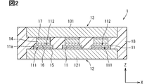
- the semiconductor device 1 includes three switching elements 11 and 11a as a plurality of semiconductor switching elements connected in parallel. More specifically, the semiconductor device 1 includes two first switching elements 11 and one second switching element 11a. Since the two first switching elements 11 have the same configuration, they are given the same reference numerals. Since one second switching element 11a has a configuration different from that of the first switching element 11, it is given a different reference numeral.
- a semiconductor device 1 including terminal members 12, 13, terminals 14, solders 15 to 17, sealing portions 18, terminals 191 to 195, and the like is adopted.
- the three switching elements 11 and 11a are packaged by the sealing portion 18. Therefore, the semiconductor device 1 can be said to be a semiconductor package.
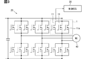
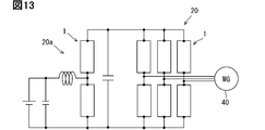
- the inverter circuit 20 is a three-phase inverter and converts DC power supplied from a battery into AC power.
- the inverter circuit 20 is electrically connected to each of the U-phase, V-phase, and W-phase of the motor generator 40.
- the inverter circuit 20 includes six semiconductor devices 1. That is, the inverter circuit 20 includes three semiconductor devices 1 as three-phase upper arm elements and three semiconductor devices 1 as three-phase lower arm elements.
- the inverter circuit 20 may include a smoothing capacitor or the like. Further, the device including the inverter circuit 20 and the control ECU 30 can be said to be a power conversion system.
- the semiconductor device 1 is electrically connected to the control ECU 30.
- the semiconductor device 1 outputs the physical information described later to the control ECU 30.
- ECU is an abbreviation for Electronic Control Unit.
- the first switching element 11 corresponds to another semiconductor switching element.
- a MOSFET is adopted as the first switching element 11.
- a MOSFET having Si as a main component or a MOSFET having SiC as a main component can be adopted. Further, the first switching element 11 can be adopted even if it is a MOSFET whose main component is another wide bandgap semiconductor.
- MOSFET is an abbreviation for metal-oxide-semiconductor field-effect transistor.
- IGBT is an abbreviation for Insulated Gate Bipolar Transistor.
- RC is an abbreviation for Reverse Conducting.
- the first switching element 11 includes a drain electrode 111 as a first main electrode formed on one surface and a source electrode 112 as a second main electrode formed on the opposite surface of one surface. ing.
- the drain electrode 111 and the source electrode 112 correspond to the main electrode.
- the first switching element 11 includes a gate electrode 113 and a Kelvin source electrode 114 as control electrodes.
- the gate electrode 113 and the Kelvin source electrode 114 are formed on opposite surfaces together with the source electrode 112.
- the first switching element 11 includes main electrodes 111 and 112 and control electrodes 113 and 114. However, the first switching element 11 does not include the detection electrode 115 provided in the second switching element 11a, which will be described later. Therefore, the first switching element 11 is different from the second switching element 11a in that the detection electrode 115 is not provided.
- the second switching element 11a corresponds to an element with a detection unit.
- the same MOSFET as the first switching element 11 is adopted as the second switching element 11a. Therefore, the second switching element 11a, like the first switching element 11, includes a drain electrode 111, a source electrode 112, a gate electrode 113, and a Kelvin source electrode 114.
- the MOSFET as the second switching element 11a similarly to the first switching element 11, a MOSFET having Si, SiC, another wide bandgap semiconductor or the like as a main component can be adopted.
- the semiconductor device 1 may include a first switching element 11 which is a MOSFET composed of SiC as a main component and an IGBT composed of Si as a main component. That is, the semiconductor device 1 can employ different types of semiconductor elements for the first switching element 11 and the second switching element 11a.
- the second switching element 11a is provided with a physical information detection unit for detecting physical information.
- a physical information detection unit for detecting physical information.
- the physical information for example, temperature and current value can be adopted. Therefore, the physical information detection unit can adopt a temperature sensitive diode, a sense source pattern, or the like. Further, it can be said that the second switching element 11a has a temperature detection function and a current detection function.
- the second switching element 11a includes a detection electrode 115. That is, the second switching element 11a includes a detection electrode 115 that the first switching element 11 does not have.
- the detection electrode 115 is electrically connected to the physical information detection unit.
- the control ECU 30 acquires an electric signal indicating physical information via the detection electrode 115.
- the electric signal is a temperature signal output by a temperature sensitive diode or a current signal output by a sense source pattern.
- the control ECU 30 may control the drive of the switching elements 11 and 11a based on the temperature signal and the current signal. For example, the control ECU 30 sets the switching elements 11 and 11a into a state in which the switching elements 11 and 11a can be driven only when the temperature signal does not reach the temperature threshold value or when the current signal does not reach the current threshold value. Then, when the temperature signal reaches the temperature threshold value, the control ECU 30 suppresses the command current and stops driving the switching elements 11 and 11a, and when the current signal reaches the current threshold value, drives and stops the switching elements 11 and 11a. ..
- control ECU 30 can protect the semiconductor device 1 by suppressing the semiconductor device 1 from becoming a high temperature state or continuing to be in a high temperature state. Further, the control ECU 30 can protect the semiconductor device 1 by suppressing the continuation of the short-circuited state of the switching elements 11 and 11a (short-circuit protection).
- the semiconductor device 1 includes three switching elements 11 and 11a.
- the three switching elements 11 and 11a are provided with a physical quantity detecting unit only in the second switching element 11a. Therefore, in the three switching elements 11 and 11a, the detection electrode 115 is provided only in the second switching element 11a.
- the drain electrode 111 and the source electrode 112 are arranged so as to be along the XY plane. Further, the three switching elements 11 and 11a are arranged side by side in the X direction. In this embodiment, as an example, an example in which the second switching element 11a is arranged at the end is adopted. However, the present disclosure is not limited to this, and the second switching element 11a may be arranged at a position sandwiched between the two first switching elements 11.
- the first terminal member 12 includes a first facing portion 121 and a first terminal portion 122.
- the first terminal member 12 is made of a metal such as aluminum or copper. As shown in FIG. 2, the first terminal member 12 is commonly provided in the three switching elements 11 and 11a.
- the first terminal member 12 is electrically connected to the drain electrodes 111 of the switching elements 11 and 11a via the first solder 15.
- the first terminal member 12 includes a first facing portion 121 and a first terminal portion 122.
- the first facing portion 121 and the first terminal portion 122 are configured as an integral body.
- the first facing portion 121 is a portion facing each of the switching elements 11 and 11a, and is electrically connected to the drain electrode 111 via the first solder 15. Further, in the first facing portion 121, the opposite side of the facing surface to the switching elements 11 and 11a is exposed from the sealing portion 18 described later. The portion exposed from the sealing portion 18 can also be said to be the exposed portion of the first facing portion 121.
- the first facing portion 121 is thermally connected to the switching elements 11 and 11a by being connected to the switching elements 11 and 11a via the first solder 15. Therefore, the heat generated by the operation of the switching elements 11 and 11a is transferred to the first facing portion 121. Then, the first facing portion 121 can dissipate the transferred heat from the exposed portion. Therefore, the first facing portion 121 has a function of cooling the switching elements 11 and 11a.
- the first terminal portion 122 is a portion protruding from a part of the first facing portion 121.
- the first terminal portion 122 is for electrically connecting the switching elements 11 and 11a and the electronic component provided outside the semiconductor device 1.
- the first terminal portion 122 is electrically connected to, for example, a bus bar.
- the first terminal member 12 has a function as a heat radiating member and a function as an electrical connecting member.
- the first facing portion 121 and the first terminal portion 122 may be configured separately. In this case, the first facing portion 121 and the first terminal portion 122 are connected via a conductive connecting member such as welding or solder.
- the second terminal member 13 includes a second facing portion 131 and a second terminal portion 132.
- the second terminal member 13 is made of the same material as the first terminal member 12, and has the same shape as the first terminal member 12.
- the second terminal member 13 is commonly provided in the three switching elements 11 and 11a.
- the second terminal member 13 is electrically connected to the source electrode 112 of each of the switching elements 11 and 11a.
- the source electrodes 112 of the switching elements 11 and 11a are electrically connected to the terminal 14 via the second solder 16.
- the terminal 14 is made of the same material as the second terminal member 13, and is, for example, a rectangular parallelepiped block body.
- the terminal 14 is individually provided corresponding to each of the switching elements 11 and 11a.
- the terminal 14 is provided to prevent the wire from coming into contact with the second terminal member.
- each terminal 14 is electrically connected to the second facing portion 131 via the third solder 17.
- the second facing portion 131 is indirectly electrically connected to the source electrodes 112 of the switching elements 11 and 11a via the terminal 14.
- the semiconductor device 1 includes a gate terminal 191 and a Kelvin source terminal 192 as control terminals which are some terminals. Further, the semiconductor device 1 includes a sense source terminal 193, an anode terminal 194, and a cathode terminal 195 as detection terminals which are a part of the terminals.
- the terminals 191 to 195 are for electrically connecting the switching elements 11 and 11a and the control ECU 30.
- the terminals 191 to 195 are made of the same material as the first terminal member 12 and the second terminal member 13.
- the terminals 191 to 195 are electrically connected to the corresponding switching elements 11 and 11a via a wire or the like.
- the gate terminal 191 and the Kelvin source terminal 192 are provided corresponding to the switching elements 11 and 11a, respectively.
- the gate terminal 191 is electrically connected to the gate electrode 113 of each of the switching elements 11 and 11a.
- the Kelvin source terminal 192 is electrically connected to the Kelvin source electrode 114 of each of the switching elements 11 and 11a.
- the sense source terminal 193, the anode terminal 194, and the cathode terminal 195 are provided only corresponding to the second switching element 11a.
- the sense source terminal 193 is electrically connected to the detection electrode 115 connected to the sense source pattern.
- the anode terminal 194 is electrically connected to the detection electrode 115 connected to the anode electrode of the temperature sensitive diode.
- the cathode terminal 195 is electrically connected to the detection electrode 115 connected to the cathode electrode of the temperature sensitive diode.
- the sealing portion 18 is made of an electrically insulating resin such as an epoxy resin.
- the sealing portion 18 collectively seals the switching elements 11 and 11a. That is, the switching elements 11 and 11a are covered by the sealing portion 18 while being in contact with the sealing portion 18.
- the sealing portion 18 covers the terminal members 12, 13 and the terminals 191 to 195 with the ends of the terminal members 12, 13 and the terminals 191 to 195 exposed. Further, the sealing portion 18 covers the first terminal member 12 and the second terminal member 13 in a state where the exposed portions of the first terminal member 12 and the second terminal member 13 are exposed. Further, the sealing portion 18 covers a portion connected by the solders 15 to 17 and a portion to which the wire is connected.
- the second switching element 11a which is a part of the plurality of switching elements 11, 11a connected in parallel, is an element with a detection unit.
- the second switching element 11a has a detection electrode 115 in addition to the main electrodes 111 and 112 and control electrodes 191 and 192.
- the first switching element 11 has main electrodes 111 and 112 and control electrodes 191, 192. Further, the first switching element 11 does not have a detection electrode 115. Therefore, in the semiconductor device 1, the number of electrodes can be reduced as compared with the configuration in which the physical information detection unit is provided in all the switching elements 11 and 11a, and it is possible to suppress the increase in physique.
- the number of terminals of the semiconductor device 1 can be reduced as compared with the configuration in which the physical information detection unit is provided in all the switching elements 11 and 11a, the cost increase can be suppressed and the configuration can be simplified.
- the number of switching elements 11 and 11a in the semiconductor device 1 is not limited to the above. If the semiconductor device 1 includes at least one second switching element 11a and at least one first switching element 11, the above effect can be obtained.
- the configuration of the semiconductor device 1 is the same as that of the above embodiment, and includes three switching elements 11 and 11a.
- the semiconductor device 1 is provided in the converter circuit 20a.
- the converter circuit 20a includes a semiconductor device 1 as an upper arm element and a semiconductor device 1 as a lower arm element. Further, each semiconductor device 1 is electrically connected to the control ECU 30a.
- the control ECU 30a is the same as the control ECU 30. Further, the device including the converter circuit 20a and the control ECU 30a can be said to be a power conversion system.
- the semiconductor device 1 can also be applied to the converter circuit 20a. Further, the semiconductor device 1 can exert the same effect as that of the above embodiment.
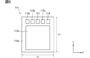
- FIGS. 5 and 6 in the semiconductor device of this embodiment, the configurations of the first switching element 11 and the second switching element 11a are different from those of the above embodiment. Note that FIG. 5 shows the detection electrode in more detail than in the first embodiment. Therefore, in the first embodiment, the configuration shown in FIG. 5 can be adopted as the second switching element 11a.
- the second switching element 11a includes a source electrode 112a, a gate electrode 113, and a Kelvin source electrode 114, as in the first embodiment. Further, the second switching element 11a includes an anode electrode 115a, a cathode electrode 115b, and a sense source electrode 115c as detection electrodes.
- the source electrode 112a is provided in the opposite region of the activation region. Therefore, the area of the activation region can be regarded as equivalent to the area of the source electrode 112a.
- the second switching element 11a is provided with a second guard ring 116a around the activation region. It is assumed that the second switching element 11a has a length in the Y direction of y1 and a length in the X direction of x1. Therefore, the area of the second switching element 11a is represented by the product of y1 and x1.
- the first switching element 11 includes a source electrode 112, a gate electrode 113, and a Kelvin source electrode 114, as in the first embodiment.
- the source electrode 112 is provided in the opposite region of the activation region. Therefore, the area of the activation region can be regarded as equivalent to the area of the source electrode 112.
- the first switching element 11 is provided with a second guard ring 116 around the activation region. It is assumed that the first switching element 11 has a length in the Y direction of y2 and a length in the X direction of x2. Therefore, the area of the first switching element 11 is represented by the product of y2 and x2. Further, the first switching element 11 has a thickness equivalent to that of the second switching element 11a.
- the area in this embodiment is the area on the XY plane.
- the thickness is the length in the Z direction.
- the relationship between the lengths of the sides of both switching elements 11 and 11a is y2 ⁇ y1 and x2 ⁇ x1. Therefore, the first switching element 11 has a smaller physique than the second switching element 11a. Further, the size (area) of the activation region of the first switching element 11 is the same as that of the second switching element 11a.
- the physique can be made smaller than that of the second switching element 11a.
- the first switching element 11 one having the same size of the activation region as the second switching element 11a can be adopted.
- the first switching element 11 may have a smaller physique than the second switching element 11a. Therefore, the relationship between the lengths of the sides of both switching elements 11 and 11a is not limited to the above.
- the semiconductor device of the present embodiment can exhibit the same effect as the semiconductor device 1. Further, the semiconductor device of the present embodiment can be smaller in size than the semiconductor device in which all the switching elements are composed of the second switching element 11a.
- the semiconductor device of this embodiment can also be implemented in combination with the first embodiment and the second embodiment. That is, the semiconductor device of this embodiment may be applied to the inverter circuit 20 or the converter circuit 20a. Further, the semiconductor device of this embodiment can be implemented in combination with other embodiments.
- the semiconductor device of the fourth embodiment will be described with reference to FIGS. 7 to 10.
- the semiconductor device of the present embodiment has the same configuration as the semiconductor device 1, and can exhibit the same effect as the semiconductor device 1. Therefore, in this embodiment, the same reference numerals as those in the first embodiment are adopted.
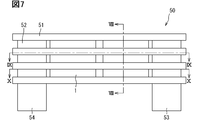
- the semiconductor device 1 is attached to a cooler 50 through which a refrigerant flows.
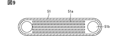
- the cooler 50 includes a plurality of facing portions 51 connected by a connecting pipe 52, and an inflow pipe 53 and an outflow pipe 54 attached to the facing portions 51.
- the cooler 50 is made of a material having high thermal conductivity, such as aluminum.
- the facing portion 51 forms a space through which the refrigerant flows, fins 51a are arranged in the space, and a water channel 51b for flowing the refrigerant is provided in the space.
- Each facing portion 51 is connected by two connecting pipes 52 through which the refrigerant flows.
- the connecting pipe 52 is connected to each water channel 51b.
- one facing portion 51 is connected to the other facing portion 51 by a connecting pipe 52, and the inflow pipe 53 and the outflow pipe 54 are attached to the water channel 51b.
- Three connecting pipes 52 are provided on the extension line of the inflow pipe 53, and three are provided on the extension line of the outflow pipe 54.
- the refrigerant is discharged from the inflow pipe 53 through the facing portion 51 and the connecting pipe 52 from the outflow pipe 54.
- the refrigerant flowing through the facing portion 51 flows from the inflow pipe 53 side to the outflow pipe 54 side. That is, the refrigerant flows into the facing portion 51 from the inflow pipe 53 and the connecting pipe 52 provided on the extension line of the inflow pipe 53. Then, the refrigerant flowing through the facing portion 51 flows out to the connecting pipe 52 and the outflow pipe 54 provided on the extension line of the outflow pipe 54.
- the refrigerant flows from the connecting pipe 52 side provided on the extension line of the inflow pipe 53 to the connecting pipe 52 side provided on the extension line of the outflow pipe 54 in the facing portion 51. Therefore, in the facing portion 51, the connecting pipe 52 side provided on the extension line of the inflow pipe 53 is the upstream side, and the connecting pipe 52 side provided on the extension line of the outflow pipe 54 is the downstream side.
- each semiconductor device 1 is arranged in contact with the facing portion 51. Further, each semiconductor device 1 may be arranged with a heat radiating member such as heat radiating grease having high thermal conductivity interposed between the semiconductor device 1 and the facing portion 51. In this case, the heat radiating member comes into contact with both the semiconductor device 1 and the facing portion 51.
- a heat radiating member such as heat radiating grease having high thermal conductivity interposed between the semiconductor device 1 and the facing portion 51. In this case, the heat radiating member comes into contact with both the semiconductor device 1 and the facing portion 51.
- each semiconductor device 1 the second switching element 11a is arranged on the downstream side with respect to the flow direction. That is, the second switching element 11a is arranged on the downstream side of the first switching element 11 with respect to the flow direction. Therefore, the temperature of the second switching element 11a tends to be higher than that of the first switching element 11. Therefore, each semiconductor device 1 can output the temperature signal of the second switching element 11a, which tends to have a high temperature.
- the temperature signal output from each semiconductor device 1 is input to the control ECU 30.
- the control ECU 30 grasps the temperature state of each semiconductor device 1 based on the temperature signal. Then, when the temperature signal reaches the threshold value, the control ECU 30 stops the operation of the switching elements 11 and 11a.
- the control ECU 30 can grasp the temperature state of each semiconductor device 1 based on the temperature of the second switching element 11a, which tends to have the highest temperature. Therefore, the control ECU 30 can easily protect the semiconductor device 1 from the high temperature state.
- the present disclosure is not limited to this, and for example, only one semiconductor device 1 may be attached to the cooler 50, or two semiconductor devices 1 may be attached to the cooler 50. Further, in the present disclosure, eight semiconductor devices 1 may be attached to the cooler 50.
- This embodiment can also be implemented in combination with the first embodiment, the second embodiment, and the third embodiment. That is, the semiconductor device 1 may be applied to the inverter circuit 20 or the converter circuit 20a, and the configurations of the first switching element 11 and the second switching element 11a may be different. Furthermore, this embodiment can also be implemented in combination with other embodiments.
- the semiconductor devices 1a and 1b of the present embodiment will be described with reference to FIG.
- the first semiconductor device 1a and the second semiconductor device 1b have the same configuration as the semiconductor device 1.
- a second switching element 11a is arranged in the first semiconductor device 1a and the second semiconductor device 1b in consideration of inductance.
- the second switching element 11a has at least a sense source pattern as a physical information detection unit.
- the parasitic inductances in the wiring on the drain side and the wiring on the source side are L1, L2, L5, L6, L9, and L10.
- the parasitic inductances in the wiring on the drain side and the wiring on the source side are L3, L4, L7, L8, L11, and L12.
- the relationship between these parasitic inductances is L1 + L2 + L3 + L4 ⁇ L5 + L6 + L7 + L8, and L1 + L2 + L3 + L4 ⁇ L9 + L10 + L11 + L12.
- the second switching element 11a is arranged at a position in the first semiconductor device 1a where current is most likely to flow. Similarly, in the second semiconductor device 1b, the second switching element 11a is arranged at a position where the current is most likely to flow in the second semiconductor device 1b.
- the semiconductor devices 1a and 1b can exert the same effect as the semiconductor device 1. Further, in the semiconductor devices 1a and 1b, since the second switching element 11a is arranged at a position where the current is most likely to flow, the short-circuit state can be quickly notified to the control ECU 30. Therefore, the semiconductor devices 1a and 1b can be reliably protected against short circuits.
- the present embodiment can also be implemented in combination with the first to fourth embodiments.
- the semiconductor device 1c of the present embodiment will be described with reference to FIG.
- the semiconductor device 1c is different from the above embodiment in that it includes three semiconductor packages 1c1, 1c2, 1c3. Similar to the first semiconductor device 1a and the second semiconductor device 1b, the semiconductor device 1c has a second switching element 11a arranged in consideration of inductance. As the switching elements 11 and 11a of the semiconductor packages 1c1, 1c2 and 1c3, the same ones as those in the above embodiment can be adopted. In particular, the second switching element 11a has at least a sense source pattern as a physical information detection unit.
- the first semiconductor package 1c1 two second switching elements 11a are connected in series. That is, in the first semiconductor package 1c1, the second switching element 11a as the upper arm element and the second switching element 11a as the lower arm element are connected in series. Further, the first semiconductor package 1c1 includes, in addition to the two second switching elements 11a, a terminal member, a control terminal, a detection terminal, a terminal, a sealing portion, and the like. Further, the first semiconductor package 1c1 includes a connecting member that electrically connects the two second switching elements 11a.
- the first semiconductor package 1c1 two second switching elements 11a, a terminal member, a control terminal, a detection terminal, a terminal, and a connecting member are sealed by a sealing portion. Similar to the semiconductor device 1, the first semiconductor package 1c1 has a part of a terminal member, a part of a control terminal, and a part of a detection terminal exposed from the sealing portion. As described above, the first semiconductor package 1c1 has a 2in1 package structure.
- the second semiconductor package 1c2 is different from the first semiconductor package 1c1 in that two first switching elements 11 are connected in series. That is, in the second semiconductor package 1c2, the first switching element 11 as the upper arm element and the first switching element 11 as the lower arm element are connected in series. Other configurations are the same as those of the first semiconductor package 1c1. Further, the third semiconductor package 1c3 has the same configuration as the second semiconductor package 1c2.
- the switching elements 11 and 11a which are the upper arm elements of the semiconductor packages 1c1 to 1c3, are connected in parallel, and the switching elements 11, 11a, which are the lower arm elements of the semiconductor packages 1c1 to 1c3, are connected in parallel. It is connected.
- the parasitic inductances in the wiring on the drain side and the wiring on the source side of each of the second switching elements 11a are L1, L2, L3, and L4.
- the parasitic inductances in the wiring on the drain side and the wiring on the source side of each first switching element 11 are L5, L6, L7, and L8.
- the parasitic inductances in the wiring on the drain side and the wiring on the source side of each first switching element 11 are L9, L10, L11, and L12.
- the parasitic inductance in the wiring on the upper arm element side is L13, L15, L17
- the parasitic inductance in the wiring on the lower arm element side is L14, L16, L18.
- the second switching element 11a is arranged at a position where the current is most likely to flow in the semiconductor device 1c. That is, in the semiconductor device 1c, two second switching elements 11a are arranged in the first semiconductor package 1c1. Therefore, the semiconductor device 1c can exert the same effect as the semiconductor devices 1a and 1b.
- the present embodiment can also be implemented in combination with the first to fourth embodiments.
- the semiconductor device 1 is provided in a power conversion device including an inverter circuit 20 and a converter circuit 20a.
- the configuration of the semiconductor device 1 is the same as that of the above embodiment, and includes three switching elements 11 and 11a.
- the inverter circuit 20 is the same as that of the first embodiment.
- the converter circuit 20a is the same as that of the second embodiment.
- the semiconductor device 1 can also be applied to a power conversion device including the inverter circuit 20 and the converter circuit 20a. Further, the semiconductor device 1 can exert the same effect as that of the above embodiment.
Landscapes
- Engineering & Computer Science (AREA)
- Power Engineering (AREA)
- Physics & Mathematics (AREA)
- Thermal Sciences (AREA)
- Microelectronics & Electronic Packaging (AREA)
- Inverter Devices (AREA)
- Cooling Or The Like Of Semiconductors Or Solid State Devices (AREA)
- Dc-Dc Converters (AREA)
- Cooling Or The Like Of Electrical Apparatus (AREA)
Applications Claiming Priority (2)
| Application Number | Priority Date | Filing Date | Title |
|---|---|---|---|
| JP2019-181661 | 2019-10-01 | ||
| JP2019181661A JP2021057534A (ja) | 2019-10-01 | 2019-10-01 | 半導体装置 |
Publications (1)
| Publication Number | Publication Date |
|---|---|
| WO2021065259A1 true WO2021065259A1 (ja) | 2021-04-08 |
Family
ID=75271272
Family Applications (1)
| Application Number | Title | Priority Date | Filing Date |
|---|---|---|---|
| PCT/JP2020/032300 Ceased WO2021065259A1 (ja) | 2019-10-01 | 2020-08-27 | 半導体装置 |
Country Status (2)
| Country | Link |
|---|---|
| JP (1) | JP2021057534A (cg-RX-API-DMAC7.html) |
| WO (1) | WO2021065259A1 (cg-RX-API-DMAC7.html) |
Citations (6)
| Publication number | Priority date | Publication date | Assignee | Title |
|---|---|---|---|---|
| WO2011111097A1 (ja) * | 2010-03-10 | 2011-09-15 | 株式会社 日立製作所 | 電力変換装置 |
| JP2013149730A (ja) * | 2012-01-18 | 2013-08-01 | Mitsubishi Electric Corp | パワー半導体モジュールおよびその製造方法 |
| JP2017011170A (ja) * | 2015-06-24 | 2017-01-12 | 株式会社デンソー | 半導体チップおよびそれを用いた半導体モジュール |
| WO2017169693A1 (ja) * | 2016-04-01 | 2017-10-05 | 三菱電機株式会社 | 半導体モジュール |
| JP2017208498A (ja) * | 2016-05-20 | 2017-11-24 | 株式会社デンソー | 半導体装置 |
| WO2018220721A1 (ja) * | 2017-05-30 | 2018-12-06 | 三菱電機株式会社 | 半導体パワーモジュール |
-
2019
- 2019-10-01 JP JP2019181661A patent/JP2021057534A/ja active Pending
-
2020
- 2020-08-27 WO PCT/JP2020/032300 patent/WO2021065259A1/ja not_active Ceased
Patent Citations (6)
| Publication number | Priority date | Publication date | Assignee | Title |
|---|---|---|---|---|
| WO2011111097A1 (ja) * | 2010-03-10 | 2011-09-15 | 株式会社 日立製作所 | 電力変換装置 |
| JP2013149730A (ja) * | 2012-01-18 | 2013-08-01 | Mitsubishi Electric Corp | パワー半導体モジュールおよびその製造方法 |
| JP2017011170A (ja) * | 2015-06-24 | 2017-01-12 | 株式会社デンソー | 半導体チップおよびそれを用いた半導体モジュール |
| WO2017169693A1 (ja) * | 2016-04-01 | 2017-10-05 | 三菱電機株式会社 | 半導体モジュール |
| JP2017208498A (ja) * | 2016-05-20 | 2017-11-24 | 株式会社デンソー | 半導体装置 |
| WO2018220721A1 (ja) * | 2017-05-30 | 2018-12-06 | 三菱電機株式会社 | 半導体パワーモジュール |
Also Published As
| Publication number | Publication date |
|---|---|
| JP2021057534A (ja) | 2021-04-08 |
Similar Documents
| Publication | Publication Date | Title |
|---|---|---|
| US10778113B2 (en) | Intelligent power module, electric vehicle, and hybrid car | |
| JP7642714B2 (ja) | 半導体装置 | |
| CN101496169B (zh) | 电力转换装置 | |
| US9236330B2 (en) | Power module | |
| CN116325135B (zh) | 半导体封装、半导体装置以及电力变换装置 | |
| US11961828B2 (en) | Semiconductor device | |
| CN111480231B (zh) | 电力转换装置 | |
| CN100428617C (zh) | 半导体元件的温度检测方法和电力变换装置 | |
| JP6576580B2 (ja) | 半導体モジュールおよび電力変換装置 | |
| JP6745991B2 (ja) | 半導体パワーモジュール | |
| JP6503909B2 (ja) | 半導体装置 | |
| WO2015107870A1 (ja) | 半導体装置 | |
| JP2014183078A (ja) | 半導体装置 | |
| JP2022050887A (ja) | 半導体装置 | |
| JP2015099846A (ja) | 半導体装置および半導体装置の製造方法 | |
| JP6123722B2 (ja) | 半導体装置 | |
| CN221486492U (zh) | 功率半导体器件、车载充电机、车辆 | |
| JP2021166247A (ja) | 半導体装置 | |
| JP6156131B2 (ja) | 半導体装置 | |
| WO2013065462A1 (ja) | 半導体装置及びその製造方法 | |
| WO2008001413A1 (en) | Power converter | |
| JP7142784B2 (ja) | 電気回路装置 | |
| JP2013105884A (ja) | 半導体モジュール | |
| JP4366269B2 (ja) | 半導体素子の温度検出方法及び電力変換装置 | |
| JP6868322B2 (ja) | 電力変換装置 |
Legal Events
| Date | Code | Title | Description |
|---|---|---|---|
| 121 | Ep: the epo has been informed by wipo that ep was designated in this application |
Ref document number: 20871938 Country of ref document: EP Kind code of ref document: A1 |
|
| NENP | Non-entry into the national phase |
Ref country code: DE |
|
| 122 | Ep: pct application non-entry in european phase |
Ref document number: 20871938 Country of ref document: EP Kind code of ref document: A1 |