WO2021054081A1 - 電極基板およびその製造方法、ならびに、そのような電極基板を用いたバイオセンサ - Google Patents
電極基板およびその製造方法、ならびに、そのような電極基板を用いたバイオセンサ Download PDFInfo
- Publication number
- WO2021054081A1 WO2021054081A1 PCT/JP2020/032501 JP2020032501W WO2021054081A1 WO 2021054081 A1 WO2021054081 A1 WO 2021054081A1 JP 2020032501 W JP2020032501 W JP 2020032501W WO 2021054081 A1 WO2021054081 A1 WO 2021054081A1
- Authority
- WO
- WIPO (PCT)
- Prior art keywords
- convex structure
- fine concavo
- thin film
- region
- conductive thin
- Prior art date
- Legal status (The legal status is an assumption and is not a legal conclusion. Google has not performed a legal analysis and makes no representation as to the accuracy of the status listed.)
- Ceased
Links
- 0 COC(C1=*c2c(*CCCCC(O*(C(CC3)=O)C3=O)=O)cccc2)=CC=CC1=C Chemical compound COC(C1=*c2c(*CCCCC(O*(C(CC3)=O)C3=O)=O)cccc2)=CC=CC1=C 0.000 description 1
Images






Classifications
-
- A—HUMAN NECESSITIES
- A61—MEDICAL OR VETERINARY SCIENCE; HYGIENE
- A61B—DIAGNOSIS; SURGERY; IDENTIFICATION
- A61B5/00—Measuring for diagnostic purposes; Identification of persons
- A61B5/145—Measuring characteristics of blood in vivo, e.g. gas concentration or pH-value ; Measuring characteristics of body fluids or tissues, e.g. interstitial fluid or cerebral tissue
- A61B5/1468—Measuring characteristics of blood in vivo, e.g. gas concentration or pH-value ; Measuring characteristics of body fluids or tissues, e.g. interstitial fluid or cerebral tissue using chemical or electrochemical methods, e.g. by polarographic means
- A61B5/1473—Measuring characteristics of blood in vivo, e.g. gas concentration or pH-value ; Measuring characteristics of body fluids or tissues, e.g. interstitial fluid or cerebral tissue using chemical or electrochemical methods, e.g. by polarographic means invasive, e.g. introduced into the body by a catheter
-
- G—PHYSICS
- G01—MEASURING; TESTING
- G01N—INVESTIGATING OR ANALYSING MATERIALS BY DETERMINING THEIR CHEMICAL OR PHYSICAL PROPERTIES
- G01N27/00—Investigating or analysing materials by the use of electric, electrochemical, or magnetic means
- G01N27/26—Investigating or analysing materials by the use of electric, electrochemical, or magnetic means by investigating electrochemical variables; by using electrolysis or electrophoresis
- G01N27/28—Electrolytic cell components
- G01N27/30—Electrodes, e.g. test electrodes; Half-cells
- G01N27/327—Biochemical electrodes, e.g. electrical or mechanical details for in vitro measurements
- G01N27/3271—Amperometric enzyme electrodes for analytes in body fluids, e.g. glucose in blood
- G01N27/3272—Test elements therefor, i.e. disposable laminated substrates with electrodes, reagent and channels
-
- A—HUMAN NECESSITIES
- A61—MEDICAL OR VETERINARY SCIENCE; HYGIENE
- A61B—DIAGNOSIS; SURGERY; IDENTIFICATION
- A61B5/00—Measuring for diagnostic purposes; Identification of persons
- A61B5/68—Arrangements of detecting, measuring or recording means, e.g. sensors, in relation to patient
- A61B5/6846—Arrangements of detecting, measuring or recording means, e.g. sensors, in relation to patient specially adapted to be brought in contact with an internal body part, i.e. invasive
- A61B5/6847—Arrangements of detecting, measuring or recording means, e.g. sensors, in relation to patient specially adapted to be brought in contact with an internal body part, i.e. invasive mounted on an invasive device
- A61B5/685—Microneedles
-
- A—HUMAN NECESSITIES
- A61—MEDICAL OR VETERINARY SCIENCE; HYGIENE
- A61B—DIAGNOSIS; SURGERY; IDENTIFICATION
- A61B2562/00—Details of sensors; Constructional details of sensor housings or probes; Accessories for sensors
- A61B2562/12—Manufacturing methods specially adapted for producing sensors for in-vivo measurements
- A61B2562/125—Manufacturing methods specially adapted for producing sensors for in-vivo measurements characterised by the manufacture of electrodes
-
- A—HUMAN NECESSITIES
- A61—MEDICAL OR VETERINARY SCIENCE; HYGIENE
- A61B—DIAGNOSIS; SURGERY; IDENTIFICATION
- A61B5/00—Measuring for diagnostic purposes; Identification of persons
- A61B5/145—Measuring characteristics of blood in vivo, e.g. gas concentration or pH-value ; Measuring characteristics of body fluids or tissues, e.g. interstitial fluid or cerebral tissue
- A61B5/14532—Measuring characteristics of blood in vivo, e.g. gas concentration or pH-value ; Measuring characteristics of body fluids or tissues, e.g. interstitial fluid or cerebral tissue for measuring glucose, e.g. by tissue impedance measurement
-
- A—HUMAN NECESSITIES
- A61—MEDICAL OR VETERINARY SCIENCE; HYGIENE
- A61B—DIAGNOSIS; SURGERY; IDENTIFICATION
- A61B5/00—Measuring for diagnostic purposes; Identification of persons
- A61B5/145—Measuring characteristics of blood in vivo, e.g. gas concentration or pH-value ; Measuring characteristics of body fluids or tissues, e.g. interstitial fluid or cerebral tissue
- A61B5/1468—Measuring characteristics of blood in vivo, e.g. gas concentration or pH-value ; Measuring characteristics of body fluids or tissues, e.g. interstitial fluid or cerebral tissue using chemical or electrochemical methods, e.g. by polarographic means
- A61B5/1486—Measuring characteristics of blood in vivo, e.g. gas concentration or pH-value ; Measuring characteristics of body fluids or tissues, e.g. interstitial fluid or cerebral tissue using chemical or electrochemical methods, e.g. by polarographic means using enzyme electrodes, e.g. with immobilised oxidase
- A61B5/14865—Measuring characteristics of blood in vivo, e.g. gas concentration or pH-value ; Measuring characteristics of body fluids or tissues, e.g. interstitial fluid or cerebral tissue using chemical or electrochemical methods, e.g. by polarographic means using enzyme electrodes, e.g. with immobilised oxidase invasive, e.g. introduced into the body by a catheter or needle or using implanted sensors
Definitions
- the present disclosure relates to an electrode substrate in which an electric circuit including a conductive thin film, an insulating coating, various electrodes, etc. is formed on an insulating substrate, and a method for manufacturing such an electrode substrate. It also relates to a biosensor using such an electrode substrate.
- the electrode substrate is manufactured by patterning a conductive thin film, an insulating coating, or the like formed on the insulating substrate. For example, in order to form an electrode pattern on an insulating substrate, first, for conduction, a conductive thin film is formed on the insulating substrate by using a technique such as sputtering. After that, various electrodes are formed at predetermined positions. Finally, it is common to coat with an insulating material to protect the electrodes. When manufacturing an electrode substrate, it is common to use various masks including a photoresist film in order to pattern a conductive thin film and various electrodes into a desired shape. Such masks also need to be stripped or dissolved and removed after patterning.
- the main body of the in-vivo type electrochemical glucose sensor is attached to the living body, and a probe having an electrode containing a sample-responsive enzyme (for example, GOx, GDH) that specifically reacts with glucose in the blood is formed in the living body. Insert and continuously measure blood glucose level. As a result, the blood glucose level can be measured for a long time without collecting blood each time.
- a probe 11 on which an electric / electronic circuit is formed is attached to the main body 10 of the glucose sensor 1.
- the tip (sensing part) of the probe 11 is inserted into the living body, and the main body 10 is attached to the living body 2 (for example, the skin of the human body) to fix it.
- the probe 11 is created using an insulating substrate without any particular limitation.
- the insulating substrate includes a substrate entirely made of resin, and a laminated substrate in which a resin layer is formed on a glass substrate or a metal substrate as a support. That is, in the present disclosure, the "insulating substrate” means a substrate having electrical insulation at least in the surface direction.
- a working electrode and a reference electrode are formed on one surface of the substrate, and a counter electrode is formed on the other surface.
- a detection layer for detecting an electrical signal due to a specific reaction between blood glucose and a sample-responsive enzyme is formed on the working electrode. This detection layer is formed by appropriately applying, for example, an aqueous suspension of conductive particles such as carbon particles, an aqueous solution of a sample-responsive enzyme, and an aqueous solution of a redox mediator, and drying.
- a conductive material selected from the group consisting of carbon or a metal such as gold, silver, platinum or palladium is sputtered over at least one surface of the insulating substrate.
- a conductive thin film is formed by depositing by a method, a vapor deposition method, an ion plating, or the like.
- an insulating region is provided on a conductive thin film and divided into a plurality of conductive regions in order to insulate between the plurality of electrodes.
- a groove reaching the surface of the insulating substrate is formed in the conductive thin film, and a lead for the working electrode and a lead for the reference electrode are provided. ..
- Such a groove is formed by forming a conductive thin film on an insulating substrate and then melting a predetermined region by laser irradiation.
- the present disclosure provides a technique for forming various electrodes in a fine circuit with good dimensional stability and easily in response to pattern miniaturization due to miniaturization of an electrode substrate.
- the present disclosers further researched, and when a smooth region and a fine concavo-convex structure region were appropriately designed on an insulating resin substrate and a conductive thin film was formed on the smooth region, the smooth region became conductive. We succeeded in making the region where the fine concavo-convex structure was formed electrically insulating.
- the fine concavo-convex structure in the present disclosure is composed of a plurality of convex portions discontinuous in at least one direction in the surface direction (top view) of the insulating substrate.
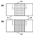
- Discontinuous protrusions include protrusions and jetties. That is, a structure in which a large number of protrusions are discontinuously arranged in at least two directions (FIG. 2a) and a structure in which a large number of jetties are discontinuously arranged in at least one direction (FIG. 2b) are microconcavo-convex structures of the present disclosure. It is effective as.
- a "fine" concavo-convex structure is a structure in which a plurality of protrusions are arranged at submicron intervals, for example, at intervals of 500 nm or less, preferably at intervals of 200 nm or less.
- the arrangement of the protrusions or jetties shown in FIG. 2 is merely an example. These protrusions and jetties can be arranged in combination.
- a fine concavo-convex structure (C1 or C2 in FIG. 2) in which a plurality of discontinuous convex portions are formed is provided between two smooth regions (A and B in FIG. 2), and the entire surface is conductive.
- the conductive thin film on the region where the fine concavo-convex structure is formed becomes discontinuous, and the two smooth regions A and B are electrically insulated from each other.
- a fine concavo-convex structure that electrically insulates two smooth regions separated by the structure is typically an insulating type. It is called a fine uneven structure.
- a structure such as a groove or unevenness having a width and a depth of several nanometers to several hundreds of microns can be formed as long as the object of the present disclosure is not impaired.
- FIG. 3a A schematic vertical cross-sectional view of the protrusion or jetty constituting the above-mentioned insulated fine uneven structure is shown in FIG. 3a (cross-sectional view taken along the I-I'cutting line of FIG. 2a). Insulated protrusions or jetties have a substantially rectangular vertical cross section.
- the insulated fine concavo-convex structure according to the present disclosure will be further described using the “projection” as an example.
- FIGS. 2a and 3a schematically depict a fine concavo-convex structure in which a plurality of protrusions are arranged.
- the fine concavo-convex structure formed on the surface of the insulating substrate is composed of columns arranged discontinuously in at least one direction.
- the "pillar" includes a substantially cylindrical cylinder and a substantially prismatic prism.
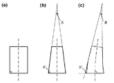
- the "substantial cylinder” is a cylinder (a) in which the angle of the generatrix with respect to the axis is 0 ° and a truncated cone (b) included in a cone having an apex angle X of 10 ° or less. (In the figure, the angle is exaggerated).
- the apex angle X exceeds 10 °, the conductive thin films are continuous between adjacent substantially cylindrical cylinders, and as a result, there is a risk of conduction.
- the lower bottom surface of the substantially cylindrical cylinder does not have to be an exact circle, and may be elliptical or irregular.
- the "substantial prism” has a shape inscribed in the substantially cylindrical cylinder described above, and the lower bottom surface thereof is also a regular polygon. It may be irregular.
- the cylinder or substantially cylinder (pillar) stands vertically or substantially vertically from the bottom of the fine concavo-convex structure.
- the upper part of the cylinder or substantially cylinder (column) is refracted or curved as long as it does not affect the insulation of the region where the fine concavo-convex structure is formed and the water repellency described later. That is, in the present disclosure, when a conductive thin film having a thickness of 5 to 100 nm, which is used in manufacturing a normal electrode substrate, is formed on the surface of an insulating substrate, the film is formed on the upper and lower surfaces of one protrusion.
- the substantially cylindrical (columnar) has a bus angle of 0 with respect to the axis.
- the intersection angle X'between the side side of such a cylinder or a substantially cylindrical (column) in the vertical cross-sectional shape and the horizontal line at the bottom of the fine concavo-convex structure may be in the range of 85 to 90 °. This will be outlined with reference to FIG. 4 (c). As an example, FIG. 4 (c). As an example, FIG.
- the intersection angle X'of the extension line of the upper part of the side side in the vertical cross-sectional shape of the substantially cylindrical cylinder and the line on the surface of the bottom surface of the fine concavo-convex structure is represented by (90-X / 2) °.
- the apex angle X of the cone is more than 0 ° and 10 ° or less, but considering the cylinder, the intersection angle X'is 85 ° or more and 90 ° or less.
- the above geometric relationship can be applied similarly when the axis of the substantially cylindrical cylinder is skewed.
- the insulating fine concavo-convex structure region is imparted with water repellency, which will be described later, while maintaining insulation. It is also possible.
- the insulated microconcavo-convex structure according to the present disclosure is composed of, for example, pillars having diagonal dimensions of 10 to 50 nm and a height of 100 to 2000 nm arranged at intervals of 50 to 200 nm as protrusions.
- the substantially cylindrical or substantially prismatic columns may be arranged at regular intervals or irregularly.
- the protrusions are aligned vertically and horizontally, but either of the vertical and horizontal directions may be arranged alternately, or may be arranged in a disorderly manner.
- the "spacing" of a pillar means the distance between the outer edges of the bottom surface of the pillar.
- Diagonal dimension is the dimension of the lower bottom surface of a pillar body, when the pillar body is a substantially cylindrical body, and when the lower bottom surface is a circle, it means the diameter thereof, and when the lower bottom surface is an ellipse. , Means its major axis. Further, in the case of a substantially prism, the lower bottom surface thereof is polygonal, which means the maximum crossing.
- the conductive thin film formed on the surface of the protrusion and the conductive thin film formed on the upper and lower surfaces of other adjacent protrusions do not directly bond; and the conductive thin film is formed on the entire side surface of the protrusion. Therefore, a conductive thin film formed on the upper and lower surfaces of one protrusion and a conductive thin film formed on the upper and lower surfaces of other adjacent protrusions are formed on the side surface of the protrusion and the bottom of the fine concavo-convex structure. The reason is that they are not indirectly bonded via the conductive thin film.
- Non-Patent Document 1 when a droplet is dropped on a substrate on which a fine uneven structure is formed, the concave portion depends on the wettability between the material of the substrate and the droplet and the shape of the concave-convex structure. It is known that the Cassie model is applied because the wettability becomes low (the water repellency becomes high) when the fluid exclusion region where the liquid cannot penetrate into the inside is large. Generally, when ⁇ is 90 ° or more, it is regarded as water repellency, when it is 110 ° or more and less than 150 °, it is regarded as high water repellency, and when it is 150 ° or more, it is regarded as super water repellency.
- the contact angle ⁇ of the water droplet on the fine concavo-convex structure is the Cassie equation of equation (1):
- ⁇ 1 represents the contact angle with respect to the smooth insulating substrate
- ⁇ 2 represents the contact angle with air
- f represents the ratio (0 to 1) of the area of the insulating substrate occupied in the fine concavo-convex structure region. .. Since the contact angle ⁇ 2 with respect to air is 180 °, Eq. (1) is Eq. (2) :.
- aqueous liquid an aqueous solution or an aqueous suspension
- water droplets are not stable on the conductive thin film, so a mask is required to obtain an electrode having an accurate shape.
- a water-repellent region is formed on the insulating substrate to define a region on which the electrode should be formed, it is possible to prevent the aqueous liquid from wetting and spreading beyond the water-repellent region without forming a mask. it can.
- a fine concavo-convex structure having water repellency is referred to as a water-repellent fine concavo-convex structure.
- the cross section of the insulated fine concavo-convex structure with improved water repellency is schematically depicted in FIG. 3b (cross-sectional view taken along the I-I'cutting line of FIG. 2a).
- the water-repellent insulated microconcavo-convex structure schematically depicted in FIG. 3b has a bottom surface having the same shape as the upper bottom surface or a lower surface than the upper bottom surface on the upper bottom surface of each of the above pillars (substantially cylindrical or substantially prismatic). It has a structure in which a cone having a small area bottom surface, that is, a substantially cone or a substantially prismatic pyramid having a shape inscribed in the substantially cone is connected.
- the fine concavo-convex structure formed on the surface of the insulating substrate has, for example, a substantially conical or a substantially pyramid on the upper and lower surfaces of a pillar having a diagonal dimension of 10 to 50 nm and a height of 100 to 2000 nm arranged at intervals of 50 to 200 nm. It is composed of connected protrusions.
- the substantially cone in FIG. 3b has a bottom surface with a diagonal dimension of 10 to 50 nm.
- the inward tilt angle of the generatrix of the substantially cone may be larger than the inclination angle of the generatrix of the substantially cylinder to which the substantially cone is connected.
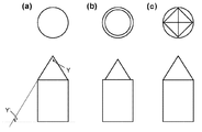
- the apex angle Y of the substantially cone is 10 to 50 °.
- the axis of the pyramid rises vertically or substantially vertically from the top and bottom surfaces of the column on which the pyramid is formed.
- the upper part of the cone it is permissible for the upper part of the cone to be refracted or curved as long as it does not affect the insulation of the region where the fine concavo-convex structure is formed and the water repellency described later. That is, in the present disclosure, when an aqueous liquid is applied to the surface of an insulating substrate to form an electrode, it is possible to prevent the aqueous liquid from wetting and spreading beyond the water-repellent region without forming a mask.
- the cone contains a cone with an apex angle Y of 10-50 °.
- the crossing angle Y' is in the range of 65 to 85 °.
- a conductive thin film with a thickness of 5 to 100 nm which is used when manufacturing a normal electrode substrate, is formed on the surface of an insulating substrate, it is formed on the upper and lower surfaces of one protrusion.
- the conductive thin film and the conductive thin film formed on the upper and lower surfaces of other adjacent protrusions are discontinuous and water repellent. The same applies to the case of a substantially pyramid.
- FIG. 5a is a schematic vertical cross-sectional view of a structure in which a substantially cone having a bottom surface having the same shape as the upper bottom surface is connected to the upper bottom surface of the substantially cylindrical cylinder.
- FIG. 5b is a schematic vertical cross-sectional view of a structure in which a substantially cone having a bottom surface having an area smaller than that of the upper bottom surface is connected to the upper bottom surface of the substantially cylindrical cylinder.
- FIG. 5c is a schematic vertical cross-sectional view of a structure in which a substantially pyramid having a bottom surface having an area smaller than that of the upper bottom surface is connected to the upper bottom surface of the substantially cylindrical cylinder.
- FIGS. 3b and 5 show a structure in which a substantially cone or a substantially pyramid is connected to the upper and lower surfaces of a substantially cylindrical cylinder, but a structure in which a substantially cone or a substantially pyramid is connected to the upper and lower surfaces of a substantially prism is also possible.
- the joint portion between the substantially cylinder and the substantially cone or the substantially pyramid is depicted as having an angle, but the joint may be smoothly connected.
- the apex of the substantially cone or the substantially pyramid is drawn sharply, it may be spherical.
- FIGS. 2a and 3 to 5 The protrusions schematically depicted in FIGS. 2a and 3 to 5 have been described, but if the vertical cross-sectional shape (cross-sectional view taken along the II-II'cutting line of FIG. 2b) is common to the protrusions, FIG. 2b A jetty outlined in can be used. That is, the intersection angle X'between the side surface in the vertical cross-sectional shape of the jetty and the horizontal plane at the bottom of the fine concavo-convex structure may be 85 to 90 °.
- the insulated microconcavo-convex structure according to the present disclosure is composed of, for example, a wall body having a bottom width of 10 to 50 nm, a length of 0.1 to 50,000 ⁇ m, and a height of 100 to 2000 nm arranged at intervals of 50 to 200 nm as a jetty.
- the plurality of wall bodies may be linear or curved in the top view, or may be refracted.
- the walls may be arranged at regular intervals or irregularly.
- the walls are arranged in parallel, but they may be arranged in a disorderly manner.
- the wall bodies extend continuously from the upper end to the lower end of the area C2, but the wall bodies may be arranged in a row with a short length.
- the "vertical cross section" of the protrusion means a cross section when the protrusion is cut in parallel with the vertical axis including the vertical axis of the substantially cylindrical cylinder defined above.
- the "vertical cross section” of the jetty is the cross section when cut perpendicular to the length direction of the wall body defined above, and when the wall body is curved or bent, the length direction is the extension thereof. It means the direction in which it exists.
- the "longitudinal section" of a pyramid means a cross section when cut parallel to and parallel to the vertical axis, including the vertical axis of the substantially cone defined above.
- a nano-order-sized fine concavo-convex structure is formed on an insulating substrate in a desired pattern, and when a conductive thin film is formed, an insulating region and a conductive region are simultaneously formed, and further.
- the insulating substrate that can be used in the present disclosure may be flexible or rigid, for example, polyethylene terephthalate (PET), polyimide (PI), polyetherimide (PEI), polyamideimide (PAI), cycloolefin polymer. It is a resin substrate such as (COP) and polyetheretherketone (PEEK). Further, a laminated substrate in which a resin film is attached to the surface of a support of a glass substrate or a metal substrate can also be used.
- a method of pressing a heated mold against a resin substrate or a resin film and heat-transferring it with a heat press or a heating roll, UV curing on the substrate A method of pressing a mold against a UV-curable resin layer of a laminated film on which a resin layer is formed and irradiating with UV can be used (for example, Patent Document 1). Further, processing techniques such as laser and quantum beam and photolithography can be applied to the film surface (Patent Document 2).
- the fine concavo-convex structure is crushed and macroscopically. It can also be flattened. Since the smooth region and the fine concavo-convex structure region depicted in FIG. 2 can be integrally molded on a single insulating substrate in a single process, the mold is pressed against the surface of the insulating substrate to form the fine concavo-convex structure. It is particularly preferable to use nanoimprinting technology as a method for forming the above.
- nanoimprinting techniques are used to form on the surface of a single insulating substrate a region in which at least one microconcavo-convex structure is formed and a plurality of smooth regions separated by the microconcavo-convex structure.
- the entire surface of the insulating substrate is then conductive, selected from metals such as carbon (C) or gold (Au), silver (Ag), copper (Cu), platinum (Pt) and palladium (Pd).
- a conductive thin film of a sex material is formed. Examples of the method for forming the conductive thin film include a sputtering method, a thin-film deposition method, and ion plating.
- a conductive material is used on the entire surface of an insulating substrate in which a region in which at least one fine concavo-convex structure is formed and a plurality of smooth regions separated by the fine concavo-convex structure are formed by using a sputtering method.
- a conductive thin film is formed by depositing.
- the entire surface of the insulating substrate can be surface-treated.
- the surface treatment method include plasma treatment such as glow discharge and corona discharge, irradiation with ultraviolet wavelength light using an excimer lamp, and surface treatment with ozone gas. These surface treatments have the effect of improving the cleanliness of the surface of the insulating substrate and generating carboxyl groups, hydroxy groups, and carbonyl groups, and activate the surface of the substrate. Adhesion is improved. Alternatively, the adhesion can be improved by roughening the surface by etching treatment, laser irradiation, ion beam irradiation, dry or wet blasting treatment, or the like.
- the base layer a material different from the conductive material for forming the conductive thin film is used in consideration of compatibility between the material of the insulating substrate and the conductive material for forming the conductive thin film.
- the base layer can be formed as one layer or a plurality of layers. Materials that can be used for the base layer are chromium (Cr), titanium (Ti), nickel (Ni), aluminum (Al), iridium (Ir), copper (Cu), tungsten (W), and indium tin oxide (ITO).
- the conductive thin film can be continuously formed in the same sputtering apparatus while maintaining the vacuum state, it is preferable to use the sputtering method for forming the underlying layer.
- the film thickness of the underlayer does not interfere with the object of the present disclosure, and specifically, it may be in the range of 10 to 100% of the conductive thin film.
- Either one of the above surface treatment and the formation of the base layer may be performed, and if there is no problem in adhesion even if the conductive thin film is formed directly on the surface of the insulating substrate, neither of them is performed. Good.
- the method for manufacturing a probe for a biosensor is an entire surface of an insulating substrate having a region on which at least one fine concavo-convex structure is formed and a plurality of smooth regions separated by the fine concavo-convex structure on the surface.
- a conductive thin film is formed on the insulating substrate. And an insulating region can be formed at the same time.
- the fine concavo-convex structure region is composed of a plurality of convex portions discontinuous in at least one direction in the surface direction of the insulating substrate, the fine concavo-convex structure region is formed on the region where the fine concavo-convex structure is formed.
- the conductive thin films are discontinuous, while the conductive thin films formed in the plurality of smooth regions separated by the fine concavo-convex structure are continuous.
- a nano-order-sized fine concavo-convex structure is formed on an insulating substrate in a desired pattern and a conductive thin film is formed on the entire surface thereof, the conductive thin film is not patterned once. If a conductive region and an insulating region can be formed on the surface, and if water repellency is imparted to the insulating microconcavo-convex structure, a highly fluid aqueous liquid can be applied to form an electrode pad with high dimensional stability. Can be done.
- a side view showing an implantable biosensor attached to a living body The schematic top view of the smooth region (A, B) and the fine concavo-convex structure region (C1, C2). Schematic vertical sectional view of a fine concavo-convex structure.
- Schematic vertical cross-sectional view of an exemplary water-repellent microconcavo-convex structure Schematic diagram showing a cross section when Au sputtering is performed on an insulating substrate on which a fine concavo-convex structure is formed: (a) a 50 nm-thick Au thin film and (b) a 150 nm-thick Au thin film are formed on the fine concavo-convex structure region.
- FIG. 10e is a cross-sectional view taken along the line III-III ′ showing the manufacturing steps (a) to (e).
- the manufacturing process of the probe of the implantable biosensor of one specific example of the present disclosure Top view of the probe front side of the implantable biosensor of one specific example of the present disclosure.
- FIG. 13 is a cross-sectional view taken along the IV-IV'cutting line in FIG.
- FIG. 14 is a cross-sectional view taken along the line V-V'in FIG.
- FIG. 14 is a cross-sectional view taken along the VI-VI'cutting line in FIG.
- the fine concavo-convex structure formed on the surface of the insulating substrate is composed of substantially cylindrical cylinders having a diameter of 10 to 50 nm and a height of 100 to 2000 nm arranged at regular intervals of 50 to 200 nm. ing.
- FIG. 6 shows a schematic view of an image obtained by observing a cross section of an Au thin film having a thickness of 50 nm (a) and a thickness of 150 nm (b) formed on an insulated fine concavo-convex structure with an electron microscope (improvement of visibility). Therefore, a schematic diagram was used).
- the 50 nm-thick Au thin film is formed on the tips of the individual protrusions forming the fine-concavo-convex structure, but is discontinuous, and the 150 nm-thick Au thin film is continuously formed on the entire micro-concavo-convex structure. was confirmed. This result is consistent with the result of the continuity test described above.
- an appropriately designed fine concavo-convex structure for example, the fine concavo-convex structure schematically depicted in FIG. 3a
- a conductive film having a thickness of 5 to 100 nm which is usually used in manufacturing an electrode substrate. Even if a flexible thin film is formed, the conductive thin film formed on the upper and lower surfaces of the protrusions constituting the fine uneven structure is not connected, and between two smooth regions separated by such a fine uneven structure. was confirmed to be electrically insulated.
- the present disclosure has, as a first aspect, a region on which at least one fine concavo-convex structure is formed and a plurality of smooth regions separated by the fine concavo-convex structure on the surface.
- An insulating substrate and a conductive thin film formed on the entire surface of at least one surface on which the fine concavo-convex structure of the insulating substrate is formed are formed, and a film is formed on the region where the fine concavo-convex structure is formed.
- an electrode substrate in which the conductive thin film is discontinuous.
- the present disclosure comprises an insulating substrate having a region on which at least one fine concavo-convex structure is formed and a plurality of smooth regions separated by the fine concavo-convex structure on the surface, and the insulating substrate.
- the fine concavo-convex structure includes a conductive thin film formed on the entire surface of at least one surface on which the fine concavo-convex structure is formed, and at least one electrode formed in a smooth region separated by the fine concavo-convex structure.
- Bio in which the conductive thin film formed on the formed region is discontinuous, and each of the two or more smooth regions separated by the region where the fine concavo-convex structure is formed is electrically insulated.
- a probe for a sensor is provided.
- the fine concavo-convex structure region is composed of a plurality of convex portions discontinuous in at least one direction in the top view of the insulating substrate.
- the plurality of protrusions discontinuous in at least one direction are pillars having a diagonal dimension of 10 to 50 nm and a height of 100 to 2000 nm (approximately a cylinder or a substantially prism) arranged at intervals of 50 to 200 nm. ).
- a substantially cone or a substantially pyramid having a bottom surface having the same shape as the upper bottom surface or a bottom surface having a smaller area than the upper bottom surface is connected to the upper bottom surface of each of the convex portions.
- the above-mentioned method for manufacturing a probe for a biosensor is provided.
- carbon, gold, silver, and copper are applied to the entire surface of an insulating substrate having a region on which at least one fine concavo-convex structure is formed and a plurality of smooth regions separated by the fine concavo-convex structure on the surface.
- the fine concavo-convex structure region is composed of a plurality of convex portions discontinuous in at least one direction in the surface direction (top view) of the insulating substrate, and is conductive formed on the region where the fine concavo-convex structure is formed.
- the thin film is discontinuous.
- a biosensor including the above-mentioned probe for the biosensor is provided.
- the embedded biosensor 1 includes the main body 10 and the probe 11, and the probe 11 is generally used for electrically connecting the sensing portion to be inserted into the living body and the internal circuit of the biosensor main body 10. It is a key shape consisting of terminal parts.
- the sensing portion is formed thin so that it can be inserted into the body, and the terminal portion has a certain size so as to be inserted into the biosensor main body 10 to form an electrical connection.
- the insulating substrate 111 is prepared (FIGS. 8a and 11a).
- PET polyethylene terephthalate
- PET polyethylene terephthalate
- a thickness of about 200 ⁇ m can be used without particular limitation as long as the material and thickness can be used as a probe to be inserted into a living body.
- PET polyethylene terephthalate
- a polyethylene terephthalate (PET) sheet Limirror R E20 # 188; 189 ⁇ m thickness manufactured by Toray Industries, Inc. was used.
- An insulating fine concavo-convex structure region 112 for forming an outer frame for forming the key-shaped probe 11 is formed on the insulating substrate 111, and the working electrode lead and the reference electrode lead are separated from each other.
- An insulating fine concavo-convex structure region 113 for forming an electrode lead for electrical insulation is formed (FIGS. 8b and 11b).
- the insulating type fine concavo-convex structure region 113 for forming electrode leads is indispensable, but if desired, the insulating type fine concavo-convex structure region 112 for forming an outer frame may not be formed.
- the fine concavo-convex structure regions 112 and 113 are insulated. Such a fine concavo-convex structure region was formed by a nanoimprinting technique of heating and pressing using a mold on which a corresponding fine concavo-convex structure was formed.
- a conductive material selected from the group consisting of carbon or a metal such as gold, silver, platinum or palladium is sputtered on an insulating substrate 111 on which a fine concavo-convex structure region is formed.
- the conductive thin film 114 is formed by depositing by a vapor deposition method, ion plating, or the like.
- the preferred thickness of the conductive thin film is 5 to 100 nm.
- a 100 nm-thick conductive thin film 114 was formed by direct gold (Au) sputtering on the insulating substrate 111 (FIGS. 9c and 11c).
- the conductive thin film 114 is divided into a working electrode lead 114a and a reference electrode lead 114b due to the presence of the insulating microconcavo-convex structure region 113 for forming the electrode lead.
- the insulating film 115a having an opening is formed by a sputtering method, a screen printing method, or the like (FIG. 9d).
- the preferred thickness of the insulating film is 0.1-40 ⁇ m.
- an insulating film having a thickness of 10 to 20 ⁇ m was formed by a screen printing method.
- an insulating film having the same shape as the insulating film 115a may be attached.
- redox mediator aqueous solution and a sample-responsive enzyme aqueous solution are mixed on the conductive thin film 114a of the sensing portion of the probe, which is not covered with the insulating film 115a, and the mixed aqueous solution is applied and dried.
- a detection layer 116b containing a redox mediator and a sample-responsive enzyme is formed (FIGS. 10e, 11e).
- the detection layer contains at least a redox mediator and a sample-responsive enzyme, and an aqueous solution of the redox mediator and an aqueous solution of the sample-responsive enzyme are sequentially applied and dried to contain the mediator layer containing the redox mediator and the sample-responsive enzyme.
- It may be a multilayer film composed of an enzyme layer.
- the preferred thickness of the detection layer is 0.1-80 ⁇ m.
- conductive particles such as a carbon particle suspension may be applied and dried first before the mixed aqueous solution of the redox mediator and the sample-responsive enzyme.
- the "specimen-responsive enzyme” means a biochemical substance capable of specifically catalyzing the oxidation or reduction of a sample. Any biochemical material may be used as long as it can be used for the purpose of detecting a biosensor.
- suitable sample-responsive enzymes include glucose oxidase (GOx) and glucose dehydrogenase (GDH).
- the "redox mediator” means a redox substance that mediates electron transfer, and is responsible for the transfer of electrons generated by the redox reaction of a sample (analyte) in a biosensor.
- a phenazine derivative and the like are included, but the present invention is not limited to this, and any redox substance may be used as long as it can be used for the detection purpose of a biosensor.
- Ketjen Black EC600JD Lion Specialty Chemicals Co., Ltd.
- a 0.2% aqueous solution of tetradecyltrimethylammonium bromide (Wako Pure Chemicals Co., Ltd.) so as to be 2 mg / ml. 0.18 ⁇ l of the resulting solution was applied to an inkjet device (Labojet3000: manufactured by Microjet Co., Ltd.) and dried.
- a conductive thin film is formed on the back side of the insulating substrate 111 in the same process as the front side, and is electrically connected to the counter electrode 118 and the main body 10.
- An insulating film 115b having an opening is formed by a sputtering method, a screen printing method, or the like in a portion excluding the region used as the counter electrode terminal 118a, and the conductivity of the sensing portion of the probe, which is not covered with the insulating film 115b, is formed.
- the sex thin film 114c is used as the counter electrode 118 (Fig. 12g).
- Individual probes are separated from the insulating substrate 111 on which a plurality of probes are formed along the insulating fine concavo-convex structure region 112 for forming an outer frame.
- the probe is separated by cutting the insulating substrate, but the cutting method is not particularly limited, and the probe can be cut by a method known in the field such as laser cutting and die cutting using a Pinnacle (registered trademark) die. ..
- One of the separated probes is shown in FIG.
- the top view of the key-shaped probe 11 as seen from the front side is shown in the upper row, and the top view seen from the back side is shown in the lower row.
- the sensing portion of the probe is immersed in a solution containing a biocompatible resin for protecting the sensor to form a protective film 119 on both sides, side surfaces and end faces of the sensing portion (FIG. 12h).
- the protective film 119 covers at least the working electrode 116, the reference electrode 117, and the counter electrode 118 without covering the working electrode terminal 116a, the reference electrode terminal 117a, and the counter electrode terminal 118a, and is inserted into the living body. Form longer than the length.
- the preferred thickness of the protective film is 5 to 200 ⁇ m.
- poly (4-vinylpyridine) can be used, and poly (4-vinylpyridine) is crosslinked with a cross-linking agent such as polyethylene glycol diglycidyl ether (PEGDGE).
- PEGDGE polyethylene glycol diglycidyl ether
- poly (tert-butyl methacrylate) -b-poly (4-vinylpyridine), polystyrene-co-4-vinylpyridine-co-oligo [propylene glycol methyl ether] methacrylate and the like can be mentioned.
- the sensing portion was immersed in an ethanol solution containing a cross-linking agent and a polymer for a protective film to form protective films (thickness 5-60 ⁇ m) on both sides, side surfaces and end faces of the sensing portion.
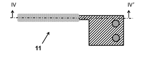
- FIG. 13 shows a top view of the probe 11 completed up to the formation of the protective film as viewed from the front side.
- a cross-sectional view taken along the IV-IV'cutting line of FIG. 13 is shown in FIG.
- Conductive thin films 114 are formed on both sides of the insulating substrate 111.
- the conductive thin film 114 on the front side is separated into two electrode leads, an working electrode lead 114a and a reference electrode lead 114b, by an insulating fine concavo-convex structure region 113 for forming electrode leads, and is electrically insulated.
- a detection layer 116b is formed on a part of the working electrode lead 114a.
- the reference electrode 117 is formed in the opening portion of the insulating film 115a and is electrically connected to the reference electrode lead 114b.
- the conductive thin film 114 on the back side serves as a counter electrode lead 114c, and a part of the conductive thin film 114 functions as a counter electrode 118.
- FIG. 14 A cross-sectional view taken along the V-V'cutting line of FIG. 14 is shown in FIG.
- a working electrode lead 114a is formed on the front side of the insulating substrate 111, and a detection layer 116b is formed on the working electrode lead 114a.
- a counter electrode lead 114c is formed on the back side of the insulating substrate 111. Furthermore, it can be seen that the entire periphery of the sensing portion is covered with the protective film 119.
- FIG. 14 A cross-sectional view of the VI-VI'cut surface of FIG. 14 is shown in FIG.
- a working electrode lead 114a and a reference electrode lead 114b electrically separated by an insulating fine concavo-convex structure region 113 for forming an electrode lead are formed, and an insulating film 115a is formed on the working electrode lead 114a.
- a reference electrode 117 is formed in the opening of the insulating film 115a.
- a counter electrode lead 114c is formed on the back side of the substrate 111, and an insulating film 115b is formed on the counter electrode lead 114c. Furthermore, it can be seen that the entire periphery of the sensing portion is covered with the protective film 119 of the present disclosure.
- an insulating substrate having a nano-sized and appropriately designed fine concavo-convex structure region is used, a very fine circuit having a wiring width and a wiring interval (line / space) on the order of several hundred nm can be used.
- An electrode substrate including the electrode substrate can be manufactured. Miniaturization can also contribute to the miniaturization of sensors. In addition, it is possible to arrange a plurality of electrodes in the conventional size, which can contribute to the production of a multifunctional sensor.
- the manufacturing method since the circuit is patterned on the insulating substrate in advance by using the nanoimprinting technique, the manufacturing process can be reduced and the manufacturing cost can be reduced.
- the fine concavo-convex structure is patterned by transfer of the mold, there is little dimensional variation at the time of manufacturing, and mass production is possible with stable circuit dimensions.
- a conductive thin film having a thickness of 5 to 100 nm is formed on the fine concavo-convex structure region, the reflectance of light is increased between the fine concavo-convex structure region and the smooth region where the fine concavo-convex structure is not formed. Since they are different, it is possible to confirm a fine circuit by using a camera or the like at the stage where the conductive thin film is formed. Due to this feature, a circuit defect can be detected before proceeding to the subsequent process, so that the yield is improved.
Landscapes
- Health & Medical Sciences (AREA)
- Life Sciences & Earth Sciences (AREA)
- Physics & Mathematics (AREA)
- Molecular Biology (AREA)
- Biophysics (AREA)
- Pathology (AREA)
- General Health & Medical Sciences (AREA)
- Chemical & Material Sciences (AREA)
- Veterinary Medicine (AREA)
- Engineering & Computer Science (AREA)
- Surgery (AREA)
- Animal Behavior & Ethology (AREA)
- Heart & Thoracic Surgery (AREA)
- Public Health (AREA)
- Biomedical Technology (AREA)
- Medical Informatics (AREA)
- Chemical Kinetics & Catalysis (AREA)
- Optics & Photonics (AREA)
- Hematology (AREA)
- Electrochemistry (AREA)
- Analytical Chemistry (AREA)
- Biochemistry (AREA)
- General Physics & Mathematics (AREA)
- Immunology (AREA)
- Emergency Medicine (AREA)
- General Chemical & Material Sciences (AREA)
- Non-Insulated Conductors (AREA)
- Apparatus Associated With Microorganisms And Enzymes (AREA)
Priority Applications (4)
| Application Number | Priority Date | Filing Date | Title |
|---|---|---|---|
| EP20864381.7A EP4033234A4 (en) | 2019-09-18 | 2020-08-28 | Electrode substrate, method for manufacturing same, and biosensor using electrode substrate |
| CN202080063678.8A CN114364313B (zh) | 2019-09-18 | 2020-08-28 | 电极基板及其制造方法以及使用了这种电极基板的生物传感器 |
| US17/641,528 US12222309B2 (en) | 2019-09-18 | 2020-08-28 | Electrode substrate, method for manufacturing same, and biosensor using electrode substrate |
| JP2021546573A JPWO2021054081A1 (https=) | 2019-09-18 | 2020-08-28 |
Applications Claiming Priority (2)
| Application Number | Priority Date | Filing Date | Title |
|---|---|---|---|
| JP2019-169161 | 2019-09-18 | ||
| JP2019169161 | 2019-09-18 |
Publications (1)
| Publication Number | Publication Date |
|---|---|
| WO2021054081A1 true WO2021054081A1 (ja) | 2021-03-25 |
Family
ID=74883479
Family Applications (1)
| Application Number | Title | Priority Date | Filing Date |
|---|---|---|---|
| PCT/JP2020/032501 Ceased WO2021054081A1 (ja) | 2019-09-18 | 2020-08-28 | 電極基板およびその製造方法、ならびに、そのような電極基板を用いたバイオセンサ |
Country Status (5)
| Country | Link |
|---|---|
| US (1) | US12222309B2 (https=) |
| EP (1) | EP4033234A4 (https=) |
| JP (1) | JPWO2021054081A1 (https=) |
| CN (1) | CN114364313B (https=) |
| WO (1) | WO2021054081A1 (https=) |
Families Citing this family (1)
| Publication number | Priority date | Publication date | Assignee | Title |
|---|---|---|---|---|
| KR102703210B1 (ko) * | 2022-01-26 | 2024-09-04 | 성균관대학교산학협력단 | 발수성 생체부착형 점착 패치 및 이의 제조방법 |
Citations (6)
| Publication number | Priority date | Publication date | Assignee | Title |
|---|---|---|---|---|
| JPH11307240A (ja) * | 1998-04-15 | 1999-11-05 | Tdk Corp | 有機el表示装置及びその製造方法 |
| CN1941384A (zh) * | 2005-09-27 | 2007-04-04 | 中华映管股份有限公司 | 有机电致发光显示器及其薄膜晶体管阵列基板的制造方法 |
| WO2011078265A1 (ja) | 2009-12-24 | 2011-06-30 | 三菱レイヨン株式会社 | 有機系離型剤の性能評価方法、モールドの製造方法および微細凹凸構造を表面に有する透明フィルムの製造方法 |
| US20160252989A1 (en) * | 2014-09-04 | 2016-09-01 | Boe Technology Group Co., Ltd. | Touch Panel and Method for Fabricating the Same |
| JP2016164691A (ja) | 2016-06-16 | 2016-09-08 | 凸版印刷株式会社 | 反射型フォトマスクおよびその製造方法 |
| WO2017187943A1 (ja) * | 2016-04-27 | 2017-11-02 | パナソニックヘルスケアホールディングス株式会社 | センサ挿入装置およびバイオセンサ |
Family Cites Families (15)
| Publication number | Priority date | Publication date | Assignee | Title |
|---|---|---|---|---|
| DE102006011545B4 (de) * | 2006-03-14 | 2016-03-17 | Robert Bosch Gmbh | Mikromechanisches Kombi-Bauelement und entsprechendes Herstellungsverfahren |
| US9549746B2 (en) * | 2007-09-28 | 2017-01-24 | The Queen's University Of Belfast | Delivery device and method |
| JP5770055B2 (ja) | 2010-09-29 | 2015-08-26 | 富士フイルム株式会社 | 針状アレイ経皮吸収シートの製造方法 |
| JP2014533523A (ja) * | 2011-09-02 | 2014-12-15 | ザ レジェンツ オブ ザ ユニヴァーシティー オブ カリフォルニア | バイオセンシングおよび薬剤供給のためのマイクロ針アレイ |
| CN203038965U (zh) * | 2012-07-02 | 2013-07-03 | 刘艳 | 发光元件 |
| US10820860B2 (en) | 2013-03-14 | 2020-11-03 | One Drop Biosensor Technologies, Llc | On-body microsensor for biomonitoring |
| GB201412696D0 (en) | 2014-07-17 | 2014-09-03 | Imp Innovations Ltd | Multi-probe microstructed arrays |
| US10172558B2 (en) | 2015-09-10 | 2019-01-08 | University Of Utah Research Foundation | Structure and methodology for a shadow mask having hollow high aspect ratio projections |
| CN105607332A (zh) * | 2016-01-04 | 2016-05-25 | 京东方科技集团股份有限公司 | 彩膜基板、显示面板和显示装置 |
| US11512384B2 (en) * | 2017-05-11 | 2022-11-29 | Medtronic Minimed, Inc. | Analyte sensors and methods for fabricating analyte sensors |
| US11077475B2 (en) | 2017-05-23 | 2021-08-03 | International Business Machines Corporation | Neuro-chemical sensor with inhibition of fouling on nano-electrode |
| US10504737B2 (en) * | 2017-05-30 | 2019-12-10 | Taiwan Semiconductor Manufacturing Co., Ltd. | Methods of enhancing surface topography on a substrate for inspection |
| EP3494875A1 (en) | 2017-12-11 | 2019-06-12 | ETH Zurich | Sensor device for detecting an electrical signal |
| EP3747364A4 (en) * | 2018-01-29 | 2021-11-10 | PHC Holdings Corporation | PROTECTIVE FILM MATERIAL FOR BIOCAPTER PROBE |
| WO2019243902A1 (en) * | 2018-06-17 | 2019-12-26 | Abdolahad Mohammad | Electrochemical biosensor and method to monitor biological cells behavior in acidic conditions |
-
2020
- 2020-08-28 JP JP2021546573A patent/JPWO2021054081A1/ja active Pending
- 2020-08-28 WO PCT/JP2020/032501 patent/WO2021054081A1/ja not_active Ceased
- 2020-08-28 EP EP20864381.7A patent/EP4033234A4/en not_active Withdrawn
- 2020-08-28 CN CN202080063678.8A patent/CN114364313B/zh active Active
- 2020-08-28 US US17/641,528 patent/US12222309B2/en active Active
Patent Citations (6)
| Publication number | Priority date | Publication date | Assignee | Title |
|---|---|---|---|---|
| JPH11307240A (ja) * | 1998-04-15 | 1999-11-05 | Tdk Corp | 有機el表示装置及びその製造方法 |
| CN1941384A (zh) * | 2005-09-27 | 2007-04-04 | 中华映管股份有限公司 | 有机电致发光显示器及其薄膜晶体管阵列基板的制造方法 |
| WO2011078265A1 (ja) | 2009-12-24 | 2011-06-30 | 三菱レイヨン株式会社 | 有機系離型剤の性能評価方法、モールドの製造方法および微細凹凸構造を表面に有する透明フィルムの製造方法 |
| US20160252989A1 (en) * | 2014-09-04 | 2016-09-01 | Boe Technology Group Co., Ltd. | Touch Panel and Method for Fabricating the Same |
| WO2017187943A1 (ja) * | 2016-04-27 | 2017-11-02 | パナソニックヘルスケアホールディングス株式会社 | センサ挿入装置およびバイオセンサ |
| JP2016164691A (ja) | 2016-06-16 | 2016-09-08 | 凸版印刷株式会社 | 反射型フォトマスクおよびその製造方法 |
Non-Patent Citations (2)
| Title |
|---|
| AKIRA NAKASHIMA: "Science and Technology of Water-repellent Solid Surface", SURFACE TECHNOLOGY, vol. 60, no. 1, 2009, pages 2 - 8 |
| See also references of EP4033234A4 |
Also Published As
| Publication number | Publication date |
|---|---|
| CN114364313A (zh) | 2022-04-15 |
| US20220334076A1 (en) | 2022-10-20 |
| JPWO2021054081A1 (https=) | 2021-03-25 |
| CN114364313B (zh) | 2024-11-29 |
| EP4033234A1 (en) | 2022-07-27 |
| EP4033234A4 (en) | 2022-11-16 |
| US12222309B2 (en) | 2025-02-11 |
Similar Documents
| Publication | Publication Date | Title |
|---|---|---|
| Dervisevic et al. | Transdermal electrochemical monitoring of glucose via high‐density silicon microneedle array patch | |
| US8696917B2 (en) | Analyte sensor and fabrication methods | |
| Xiang et al. | Ultra-thin flexible polyimide neural probe embedded in a dissolvable maltose-coated microneedle | |
| CA3056105C (en) | Metal pillar device structures and methods for making and using them in electrochemical and/or electrocatalytic applications | |
| CN111272850B (zh) | 葡萄糖传感器的工作电极 | |
| TW200901937A (en) | System and methods of chemistry patterning for a multiple well biosensor | |
| TW200819745A (en) | System and methods for determining an analyte concentration incorporating a hematocrit correction | |
| CN113567522A (zh) | 一种生物传感器及其制备方法 | |
| CA2502277A1 (en) | Analyte sensors and methods for making them | |
| WO2008021758A1 (en) | Methods for fabricating a biosensor with a surface texture | |
| JP6603554B2 (ja) | 導電性フィルム | |
| CN115644866A (zh) | Sebs在作为植入式生物电极基底中的应用以及一种植入式生物电极 | |
| US11638539B2 (en) | Needles for measurement of body fluid analytes such as glucose | |
| WO2021054081A1 (ja) | 電極基板およびその製造方法、ならびに、そのような電極基板を用いたバイオセンサ | |
| TW202227812A (zh) | 製備工作電極之方法 | |
| JP2025513665A (ja) | 電気化学的および電気生理学的測定または刺激のための光学的に透明なマイクロ電極アレイ | |
| JP2013154010A (ja) | 電気化学センサの製造方法、及び電気化学センサ | |
| CN110935495B (zh) | Gaba和电生理微纳同步传感检测芯片及其制备方法 | |
| Srikantharajah | Development, characterization, and application of compliant intracortical implants | |
| CN115175613A (zh) | 传感器及其制造方法 | |
| JP2023525172A (ja) | 試料中の中性検体を検出するための試験ストリップ | |
| de Eulate et al. | Transparent transfer-free multilayer graphene microelectrodes enable high quality recordings in brain slices | |
| HK40111866A (zh) | 分析物传感器及其制造方法 | |
| HK40099026A (zh) | 用於制造分析物传感器的至少一个电极的方法 | |
| TW201115141A (en) | capable of easily manufacturing the biochemical sensing specimen with low cost |
Legal Events
| Date | Code | Title | Description |
|---|---|---|---|
| 121 | Ep: the epo has been informed by wipo that ep was designated in this application |
Ref document number: 20864381 Country of ref document: EP Kind code of ref document: A1 |
|
| ENP | Entry into the national phase |
Ref document number: 2021546573 Country of ref document: JP Kind code of ref document: A |
|
| NENP | Non-entry into the national phase |
Ref country code: DE |
|
| ENP | Entry into the national phase |
Ref document number: 2020864381 Country of ref document: EP Effective date: 20220419 |
|
| WWW | Wipo information: withdrawn in national office |
Ref document number: 2020864381 Country of ref document: EP |