WO2021024643A1 - 半導体装置 - Google Patents
半導体装置 Download PDFInfo
- Publication number
- WO2021024643A1 WO2021024643A1 PCT/JP2020/025212 JP2020025212W WO2021024643A1 WO 2021024643 A1 WO2021024643 A1 WO 2021024643A1 JP 2020025212 W JP2020025212 W JP 2020025212W WO 2021024643 A1 WO2021024643 A1 WO 2021024643A1
- Authority
- WO
- WIPO (PCT)
- Prior art keywords
- line
- semiconductor device
- gate
- voltage
- nmos transistor
- Prior art date
- Legal status (The legal status is an assumption and is not a legal conclusion. Google has not performed a legal analysis and makes no representation as to the accuracy of the status listed.)
- Ceased
Links
Images




Classifications
-
- H—ELECTRICITY
- H03—ELECTRONIC CIRCUITRY
- H03K—PULSE TECHNIQUE
- H03K17/00—Electronic switching or gating, i.e. not by contact-making and –breaking
- H03K17/51—Electronic switching or gating, i.e. not by contact-making and –breaking characterised by the components used
- H03K17/56—Electronic switching or gating, i.e. not by contact-making and –breaking characterised by the components used by the use, as active elements, of semiconductor devices
- H03K17/687—Electronic switching or gating, i.e. not by contact-making and –breaking characterised by the components used by the use, as active elements, of semiconductor devices the devices being field-effect transistors
-
- H—ELECTRICITY
- H10—SEMICONDUCTOR DEVICES; ELECTRIC SOLID-STATE DEVICES NOT OTHERWISE PROVIDED FOR
- H10D—INORGANIC ELECTRIC SEMICONDUCTOR DEVICES
- H10D84/00—Integrated devices formed in or on semiconductor substrates that comprise only semiconducting layers, e.g. on Si wafers or on GaAs-on-Si wafers
- H10D84/80—Integrated devices formed in or on semiconductor substrates that comprise only semiconducting layers, e.g. on Si wafers or on GaAs-on-Si wafers characterised by the integration of at least one component covered by groups H10D12/00 or H10D30/00, e.g. integration of IGFETs
- H10D84/811—Combinations of field-effect devices and one or more diodes, capacitors or resistors
-
- H—ELECTRICITY
- H01—ELECTRIC ELEMENTS
- H01M—PROCESSES OR MEANS, e.g. BATTERIES, FOR THE DIRECT CONVERSION OF CHEMICAL ENERGY INTO ELECTRICAL ENERGY
- H01M10/00—Secondary cells; Manufacture thereof
- H01M10/42—Methods or arrangements for servicing or maintenance of secondary cells or secondary half-cells
-
- H—ELECTRICITY
- H02—GENERATION; CONVERSION OR DISTRIBUTION OF ELECTRIC POWER
- H02M—APPARATUS FOR CONVERSION BETWEEN AC AND AC, BETWEEN AC AND DC, OR BETWEEN DC AND DC, AND FOR USE WITH MAINS OR SIMILAR POWER SUPPLY SYSTEMS; CONVERSION OF DC OR AC INPUT POWER INTO SURGE OUTPUT POWER; CONTROL OR REGULATION THEREOF
- H02M1/00—Details of apparatus for conversion
- H02M1/08—Circuits specially adapted for the generation of control voltages for semiconductor devices incorporated in static converters
-
- H—ELECTRICITY
- H03—ELECTRONIC CIRCUITRY
- H03K—PULSE TECHNIQUE
- H03K17/00—Electronic switching or gating, i.e. not by contact-making and –breaking
- H03K17/04—Modifications for accelerating switching
-
- H—ELECTRICITY
- H10—SEMICONDUCTOR DEVICES; ELECTRIC SOLID-STATE DEVICES NOT OTHERWISE PROVIDED FOR
- H10D—INORGANIC ELECTRIC SEMICONDUCTOR DEVICES
- H10D30/00—Field-effect transistors [FET]
- H10D30/60—Insulated-gate field-effect transistors [IGFET]
- H10D30/64—Double-diffused metal-oxide semiconductor [DMOS] FETs
- H10D30/66—Vertical DMOS [VDMOS] FETs
- H10D30/668—Vertical DMOS [VDMOS] FETs having trench gate electrodes, e.g. UMOS transistors
-
- H—ELECTRICITY
- H10—SEMICONDUCTOR DEVICES; ELECTRIC SOLID-STATE DEVICES NOT OTHERWISE PROVIDED FOR
- H10D—INORGANIC ELECTRIC SEMICONDUCTOR DEVICES
- H10D84/00—Integrated devices formed in or on semiconductor substrates that comprise only semiconducting layers, e.g. on Si wafers or on GaAs-on-Si wafers
- H10D84/01—Manufacture or treatment
- H10D84/0123—Integrating together multiple components covered by H10D12/00 or H10D30/00, e.g. integrating multiple IGBTs
- H10D84/0126—Integrating together multiple components covered by H10D12/00 or H10D30/00, e.g. integrating multiple IGBTs the components including insulated gates, e.g. IGFETs
- H10D84/0149—Manufacturing their interconnections or electrodes, e.g. source or drain electrodes
-
- H—ELECTRICITY
- H10—SEMICONDUCTOR DEVICES; ELECTRIC SOLID-STATE DEVICES NOT OTHERWISE PROVIDED FOR
- H10D—INORGANIC ELECTRIC SEMICONDUCTOR DEVICES
- H10D84/00—Integrated devices formed in or on semiconductor substrates that comprise only semiconducting layers, e.g. on Si wafers or on GaAs-on-Si wafers
- H10D84/01—Manufacture or treatment
- H10D84/0123—Integrating together multiple components covered by H10D12/00 or H10D30/00, e.g. integrating multiple IGBTs
- H10D84/0126—Integrating together multiple components covered by H10D12/00 or H10D30/00, e.g. integrating multiple IGBTs the components including insulated gates, e.g. IGFETs
- H10D84/016—Integrating together multiple components covered by H10D12/00 or H10D30/00, e.g. integrating multiple IGBTs the components including insulated gates, e.g. IGFETs the components including vertical IGFETs
-
- H—ELECTRICITY
- H10—SEMICONDUCTOR DEVICES; ELECTRIC SOLID-STATE DEVICES NOT OTHERWISE PROVIDED FOR
- H10D—INORGANIC ELECTRIC SEMICONDUCTOR DEVICES
- H10D84/00—Integrated devices formed in or on semiconductor substrates that comprise only semiconducting layers, e.g. on Si wafers or on GaAs-on-Si wafers
- H10D84/01—Manufacture or treatment
- H10D84/02—Manufacture or treatment characterised by using material-based technologies
- H10D84/03—Manufacture or treatment characterised by using material-based technologies using Group IV technology, e.g. silicon technology or silicon-carbide [SiC] technology
- H10D84/038—Manufacture or treatment characterised by using material-based technologies using Group IV technology, e.g. silicon technology or silicon-carbide [SiC] technology using silicon technology, e.g. SiGe
-
- H—ELECTRICITY
- H10—SEMICONDUCTOR DEVICES; ELECTRIC SOLID-STATE DEVICES NOT OTHERWISE PROVIDED FOR
- H10D—INORGANIC ELECTRIC SEMICONDUCTOR DEVICES
- H10D84/00—Integrated devices formed in or on semiconductor substrates that comprise only semiconducting layers, e.g. on Si wafers or on GaAs-on-Si wafers
- H10D84/101—Integrated devices comprising main components and built-in components, e.g. IGBT having built-in freewheel diode
- H10D84/141—VDMOS having built-in components
- H10D84/143—VDMOS having built-in components the built-in components being PN junction diodes
- H10D84/144—VDMOS having built-in components the built-in components being PN junction diodes in antiparallel diode configurations
-
- H—ELECTRICITY
- H10—SEMICONDUCTOR DEVICES; ELECTRIC SOLID-STATE DEVICES NOT OTHERWISE PROVIDED FOR
- H10D—INORGANIC ELECTRIC SEMICONDUCTOR DEVICES
- H10D84/00—Integrated devices formed in or on semiconductor substrates that comprise only semiconducting layers, e.g. on Si wafers or on GaAs-on-Si wafers
- H10D84/80—Integrated devices formed in or on semiconductor substrates that comprise only semiconducting layers, e.g. on Si wafers or on GaAs-on-Si wafers characterised by the integration of at least one component covered by groups H10D12/00 or H10D30/00, e.g. integration of IGFETs
- H10D84/82—Integrated devices formed in or on semiconductor substrates that comprise only semiconducting layers, e.g. on Si wafers or on GaAs-on-Si wafers characterised by the integration of at least one component covered by groups H10D12/00 or H10D30/00, e.g. integration of IGFETs of only field-effect components
- H10D84/83—Integrated devices formed in or on semiconductor substrates that comprise only semiconducting layers, e.g. on Si wafers or on GaAs-on-Si wafers characterised by the integration of at least one component covered by groups H10D12/00 or H10D30/00, e.g. integration of IGFETs of only field-effect components of only insulated-gate FETs [IGFET]
- H10D84/837—Integrated devices formed in or on semiconductor substrates that comprise only semiconducting layers, e.g. on Si wafers or on GaAs-on-Si wafers characterised by the integration of at least one component covered by groups H10D12/00 or H10D30/00, e.g. integration of IGFETs of only field-effect components of only insulated-gate FETs [IGFET] comprising vertical IGFETs
- H10D84/839—Integrated devices formed in or on semiconductor substrates that comprise only semiconducting layers, e.g. on Si wafers or on GaAs-on-Si wafers characterised by the integration of at least one component covered by groups H10D12/00 or H10D30/00, e.g. integration of IGFETs of only field-effect components of only insulated-gate FETs [IGFET] comprising vertical IGFETs comprising VDMOS
-
- H—ELECTRICITY
- H10—SEMICONDUCTOR DEVICES; ELECTRIC SOLID-STATE DEVICES NOT OTHERWISE PROVIDED FOR
- H10D—INORGANIC ELECTRIC SEMICONDUCTOR DEVICES
- H10D89/00—Aspects of integrated devices not covered by groups H10D84/00 - H10D88/00
- H10D89/211—Design considerations for internal polarisation
- H10D89/213—Design considerations for internal polarisation in field-effect devices
- H10D89/215—Design considerations for internal polarisation in field-effect devices comprising arrangements for charge pumping or biasing substrates
-
- H—ELECTRICITY
- H10—SEMICONDUCTOR DEVICES; ELECTRIC SOLID-STATE DEVICES NOT OTHERWISE PROVIDED FOR
- H10D—INORGANIC ELECTRIC SEMICONDUCTOR DEVICES
- H10D89/00—Aspects of integrated devices not covered by groups H10D84/00 - H10D88/00
- H10D89/60—Integrated devices comprising arrangements for electrical or thermal protection, e.g. protection circuits against electrostatic discharge [ESD]
- H10D89/601—Integrated devices comprising arrangements for electrical or thermal protection, e.g. protection circuits against electrostatic discharge [ESD] for devices having insulated gate electrodes, e.g. for IGFETs or IGBTs
- H10D89/611—Integrated devices comprising arrangements for electrical or thermal protection, e.g. protection circuits against electrostatic discharge [ESD] for devices having insulated gate electrodes, e.g. for IGFETs or IGBTs using diodes as protective elements
-
- H—ELECTRICITY
- H10—SEMICONDUCTOR DEVICES; ELECTRIC SOLID-STATE DEVICES NOT OTHERWISE PROVIDED FOR
- H10D—INORGANIC ELECTRIC SEMICONDUCTOR DEVICES
- H10D89/00—Aspects of integrated devices not covered by groups H10D84/00 - H10D88/00
- H10D89/60—Integrated devices comprising arrangements for electrical or thermal protection, e.g. protection circuits against electrostatic discharge [ESD]
- H10D89/601—Integrated devices comprising arrangements for electrical or thermal protection, e.g. protection circuits against electrostatic discharge [ESD] for devices having insulated gate electrodes, e.g. for IGFETs or IGBTs
- H10D89/811—Integrated devices comprising arrangements for electrical or thermal protection, e.g. protection circuits against electrostatic discharge [ESD] for devices having insulated gate electrodes, e.g. for IGFETs or IGBTs using FETs as protective elements
- H10D89/813—Integrated devices comprising arrangements for electrical or thermal protection, e.g. protection circuits against electrostatic discharge [ESD] for devices having insulated gate electrodes, e.g. for IGFETs or IGBTs using FETs as protective elements specially adapted to provide an electrical current path other than the field-effect induced current path
- H10D89/814—Integrated devices comprising arrangements for electrical or thermal protection, e.g. protection circuits against electrostatic discharge [ESD] for devices having insulated gate electrodes, e.g. for IGFETs or IGBTs using FETs as protective elements specially adapted to provide an electrical current path other than the field-effect induced current path involving a parasitic bipolar transistor triggered by the electrical biasing of the gate electrode of the FET, e.g. gate coupled transistors
-
- H—ELECTRICITY
- H10—SEMICONDUCTOR DEVICES; ELECTRIC SOLID-STATE DEVICES NOT OTHERWISE PROVIDED FOR
- H10W—GENERIC PACKAGES, INTERCONNECTIONS, CONNECTORS OR OTHER CONSTRUCTIONAL DETAILS OF DEVICES COVERED BY CLASS H10
- H10W20/00—Interconnections in chips, wafers or substrates
- H10W20/40—Interconnections external to wafers or substrates, e.g. back-end-of-line [BEOL] metallisations or vias connecting to gate electrodes
- H10W20/41—Interconnections external to wafers or substrates, e.g. back-end-of-line [BEOL] metallisations or vias connecting to gate electrodes characterised by their conductive parts
- H10W20/427—Power or ground buses
-
- H—ELECTRICITY
- H10—SEMICONDUCTOR DEVICES; ELECTRIC SOLID-STATE DEVICES NOT OTHERWISE PROVIDED FOR
- H10D—INORGANIC ELECTRIC SEMICONDUCTOR DEVICES
- H10D84/00—Integrated devices formed in or on semiconductor substrates that comprise only semiconducting layers, e.g. on Si wafers or on GaAs-on-Si wafers
- H10D84/80—Integrated devices formed in or on semiconductor substrates that comprise only semiconducting layers, e.g. on Si wafers or on GaAs-on-Si wafers characterised by the integration of at least one component covered by groups H10D12/00 or H10D30/00, e.g. integration of IGFETs
- H10D84/82—Integrated devices formed in or on semiconductor substrates that comprise only semiconducting layers, e.g. on Si wafers or on GaAs-on-Si wafers characterised by the integration of at least one component covered by groups H10D12/00 or H10D30/00, e.g. integration of IGFETs of only field-effect components
- H10D84/83—Integrated devices formed in or on semiconductor substrates that comprise only semiconducting layers, e.g. on Si wafers or on GaAs-on-Si wafers characterised by the integration of at least one component covered by groups H10D12/00 or H10D30/00, e.g. integration of IGFETs of only field-effect components of only insulated-gate FETs [IGFET]
- H10D84/83125—Integrated devices formed in or on semiconductor substrates that comprise only semiconducting layers, e.g. on Si wafers or on GaAs-on-Si wafers characterised by the integration of at least one component covered by groups H10D12/00 or H10D30/00, e.g. integration of IGFETs of only field-effect components of only insulated-gate FETs [IGFET] the IGFETs characterised by having shared source or drain regions
-
- Y—GENERAL TAGGING OF NEW TECHNOLOGICAL DEVELOPMENTS; GENERAL TAGGING OF CROSS-SECTIONAL TECHNOLOGIES SPANNING OVER SEVERAL SECTIONS OF THE IPC; TECHNICAL SUBJECTS COVERED BY FORMER USPC CROSS-REFERENCE ART COLLECTIONS [XRACs] AND DIGESTS
- Y02—TECHNOLOGIES OR APPLICATIONS FOR MITIGATION OR ADAPTATION AGAINST CLIMATE CHANGE
- Y02E—REDUCTION OF GREENHOUSE GAS [GHG] EMISSIONS, RELATED TO ENERGY GENERATION, TRANSMISSION OR DISTRIBUTION
- Y02E60/00—Enabling technologies; Technologies with a potential or indirect contribution to GHG emissions mitigation
- Y02E60/10—Energy storage using batteries
Definitions
- the present invention relates to a semiconductor device.
- An ECU Electric Control Unit
- a battery in a general automobile and a load such as a motor is provided with a switch for supplying electric power from the battery to the load (for example, Patent Document 1).
- a switch for supplying electric power to a load for example, two MOS transistors having a common gate electrode (particularly, an NMOS transistor) may be used.
- two MOS transistors having a common gate electrode particularly, an NMOS transistor
- the gate capacitance of the two MOS transistors constituting the switch is large, there is a problem that the switching period when the switch is turned on and off becomes long.
- the present invention has been made in view of the above-mentioned conventional problems, and an object of the present invention is to provide a semiconductor device including a switch capable of shortening a switching period.
- the main invention for solving the above-mentioned problems is with the first and second MOS transistors in which drain electrodes are connected in series between the first line to which the power supply voltage is applied and the second line to which the load is connected.
- a third line connected to the gate electrode of the first MOS transistor and a fourth line connected to the gate electrode of the second MOS transistor and electrically separated from the third line are provided. It is a semiconductor device characterized by.
- a semiconductor device including a switch capable of shortening the switching period.
- FIG. 1 is a diagram showing a configuration of a motor control device 10 according to an embodiment of the present invention.
- the motor control device 10 is a device for controlling a motor 12 provided in an automobile by using electric power from a battery 11, and has an ECU 20 including an IPS (Intelligent Power Switch) 21.
- the battery 11 is, for example, a lithium-ion battery for automobiles, and outputs a power supply voltage Vcc of 12 V.
- the ECU 20 is a device that controls the motor 12, and includes an IPS 21 (described later), a microcomputer 30, and a switch 31.
- the microcomputer 30 controls the IPS 21 and the switch 31 based on an instruction (not shown) input from the outside.
- the switch 31 is an element for applying the power supply voltage Vcc of the battery 11 output via the IPS 21 to the motor 12.
- the microcomputer 30 will be described as having the switch 31 turned on.
- the IPS 21 is a "semiconductor device” that switches whether or not to supply the power supply voltage Vcc of the battery 11 to the motor 12 based on the instruction signal Sa output from the microcomputer 30.
- the IPS 21 includes terminals VCS, GND, IN, and OUT, the power supply voltage Vcc of the battery 11 is applied to the terminal VCS, and the terminal GND is grounded. Further, the instruction signal Sa from the microcomputer 30 is input to the terminal IN, and the voltage Vcc is output from the terminal OUT when the switch (described later) inside the IPS 21 is turned on. In this embodiment, the voltage of the terminal GND is set to the ground voltage Vgnd (0V).
- the IPS 21 appropriately protects the motor 12 and the ECU 20 when the battery 11 is reversely connected.
- the "reverse connection” is a state in which the positive electrode of the battery 11 is connected to a terminal on the ground side (for example, terminal GND) and the negative electrode of the battery 11 is connected to a terminal on the power supply side (for example, terminal VCS).
- FIG. 2 is a diagram showing an example of the configuration of IPS 21.
- the IPS 21 includes an IC (Integrated Circuit) 50 on which a switch (described later) is formed, and an IC 51 having a circuit for turning the switch on and off.
- IC Integrated Circuit
- the IC50 includes two MOS transistors constituting a switch (hereinafter, referred to as "switch X1") for switching whether or not to output the power supply voltage Vcc from the terminal OUT.
- switch X1 a switch
- the two transistors are NMOS transistors M1 and M2.
- the source electrode S1 is connected to the "power supply line L1" to which the power supply voltage Vcc is applied. Further, a diode 60 is formed as a body diode between the source electrode S1 of the NMOS transistor M1 and the drain electrode D1.
- the source electrode S2 is connected to the "load line L2" to which the load of the ECU 20 or the like is connected, and the drain electrode D2 is connected to the drain electrode D1 of the NMOS transistor M1. Further, a diode 61 is formed as a body diode between the source electrode S2 of the NMOS transistor M2 and the drain electrode D2.
- the drain electrodes D1 and D2 of the NMOS transistors M1 and M2 are connected in series to each other, when both the NMOS transistors M1 and M2 are turned on, the power supply voltage Vcc of the terminal VCC is output from the terminal OUT. Will be.
- the anode of the diode 60 is connected to the power supply line L1
- the cathode of the diode 60 is connected to the cathode of the diode 61.
- the anode of the diode 61 is connected to the load line L2. Therefore, the diodes 60 and 61 provided between the power supply line L1 and the load line L2 are connected so that their cathodes face each other.
- the power supply voltage Vcc applied to the terminal VCS is cut off by the diode 61.
- the power supply voltage Vcc of the terminal OUT is cut off by the diode 60.
- the "switch X1" can prevent the current from flowing to the load connected to the terminal OUT, so that the load is appropriately protected.
- the NMOS transistor M1 corresponds to the "first MOS transistor”
- the NMOS transistor M2 corresponds to the "second MOS transistor”.
- the power supply line L1 corresponds to the "first line”
- the load line L2 corresponds to the "second line”.
- FIG. 3 is a diagram showing a cross section of the NMOS transistors M1 and M2.
- the NMOS transistors M1 and M2 are formed on the semiconductor substrate 200 of the IC50.
- the semiconductor substrate 200 is, for example, an n-type substrate made of silicon, and drain electrodes 210 are formed on the back surface side, source electrodes 211a and 211b and substrate electrodes 212a and 212b are formed on the front surface side.
- the drain electrode 210, the source electrodes 211a and 211b, and the substrate electrodes 212a and 212b may be formed of a conductive material such as polysilicon or a metal electrode. Since the structures of the NMOS transistors M1 and M2 are the same, the NMOS transistors M1 will be described below.
- the electrodes of the NMOS transistors M1 and M2 are designated by different reference numerals for convenience, but the drain electrode 210 of the NMOS transistor M1 corresponds to the “drain electrode D1” and the source electrode 211a. Corresponds to "source electrode S1". Further, the gate electrode 241a (described later) corresponds to the “gate electrode G1”.
- an n-type drift region 220, an n + -type drain region 221, a p-type well region 222a, an n + -type source region 223a, a p + -type contact region 224a, and a gate trench portion 230a are formed inside the semiconductor substrate 200.
- the drift region 220 is a region containing n-type impurities such as phosphorus, and the drain region 221 contains n-type impurities such as phosphorus at a higher concentration than the drift region 220 and is formed on the back surface side of the drift region 220. Area.
- the well region 222a is a region formed on the surface side of the drift region 220, and the source region 223a is an n + type region formed in a part of the well region 222a.
- n + type or p + type it means that the doping concentration is higher than that of n type or p type.
- a p + type contact region 224a containing a high concentration of p-type impurities is formed from the well region 222a.
- a diode 60 which is a body diode, is formed between the p-type well region 222a and the n-type drift region 220.
- the gate trench portion 230a includes a gate oxide film 240a formed on the inner wall of the trench and a gate electrode 241a in the trench covered with the gate oxide film 240a.
- the gate electrode 241a is made of a conductive material such as polysilicon. Further, the gate trench portion 230a is covered with an oxide film 231a, and a source electrode 211a is formed on the surface side of the oxide film 231a so as to cover the oxide film 231a.
- the drain electrode 210 of the NMOS transistor M2 corresponds to the “drain electrode D2”
- the source electrode 211b corresponds to the “source electrode S2”.
- the gate electrode 241b corresponds to the “gate electrode G2”.
- the IC 51 of FIG. 2 is a circuit for turning on / off the “switch X1” based on the instruction signal Sa, and is a power supply circuit 70, a control circuit 71, a charge pump circuit 72, a separation circuit 73, a discharge circuit 74, and a gate protection circuit. It is composed of 75, 76, and resistors 80-82.
- the power supply circuit 70 generates a power supply voltage Vdd for operating circuits such as the control circuit 71 and the charge pump circuit 72 based on the power supply voltage Vcc from the battery 11.
- the power supply voltage Vdd is a voltage lower than the power supply voltage Vcc.
- the control circuit 71 Based on the instruction signal Sa, the control circuit 71 has an instruction signal Sb (first instruction signal) for turning on the "switch X1" and an instruction signal Sc (second instruction signal) for turning off the "switch X1". And, it is a logic circuit that generates.
- the charge pump circuit 72 is a circuit that generates a predetermined voltage Vcp (predetermined voltage) for turning on the NMOS transistors M1 and M2 constituting the "switch X1" based on the instruction signal Sb. The details of the charge pump circuit 72 will be described later.
- the separation circuit 73 is a circuit that applies a voltage corresponding to the voltage Vcp to the two lines in a state where the two lines (described later) to which the gate electrodes of the NMOS transistors M1 and M2 are connected are electrically separated. is there.
- the separation circuit 73 includes diodes 100 to 103 and resistors 104 and 105.
- a voltage Vcp is applied to the anode of the diode 100, and the cathode is connected to the anode of the diode 101.
- the cathode of the diode 101 is connected to one end of the resistor 104 and the other end of the resistor 104 is connected to the gate line L3.
- the gate line L3 is a wiring connected to the gate electrode G1 of the NMOS transistor M1 via the resistor 80.
- a voltage Vcp is applied to the anode of the diode 102, and the cathode is connected to the anode of the diode 103.
- the cathode of the diode 103 is connected to one end of the resistor 105 and the other end of the resistor 105 is connected to the gate line L4.
- the gate line L4 is a wiring connected to the gate electrode G2 of the NMOS transistor M2 via the resistor 81.
- the diodes 100, 101 and the resistor 104 connected in series apply a voltage corresponding to the voltage Vcp only to the gate line L3 among the gate lines L3 and L4.
- the diodes 102 and 103 and the resistor 105 connected in series apply a voltage corresponding to the voltage Vcp only to the gate line L4 among the gate lines L3 and L4.
- two diodes are connected to the gate lines L3 and L4, but another number (for example, one or three or more) may be used.
- the gate line L3 may be any "wiring that electrically connects the output from the separation circuit 73 and the gate electrode G1". Therefore, the gate line L3 does not have to include the resistor 80.
- the gate line L4 is the same as the gate line L3. Here, the gate line L3 corresponds to the "third line”, and the gate line L4 corresponds to the "fourth line”. Further, each of the diodes 100 and 101 corresponds to the "first diode”, and each of the diodes 102 and 103 corresponds to the "second diode".
- the discharge circuit 74 is a circuit for turning off the NMOS transistors M1 and M2 constituting the "switch X1", and includes the NMOS transistors 120 and the switches 121 and 122.
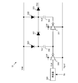
- the NMOS transistor 120 is a depletion type transistor, the drain electrode D3 is connected to the gate line L3, and the gate electrode G3 and the source electrode S3 are connected to the load line L2 via the resistor 82. Therefore, since the NMOS transistor 120 is always on, the gate capacitance of the NMOS transistor M1 is discharged via the NMOS transistor 120.
- the current value when the NMOS transistor 120 discharges the gate capacitance of the NMOS transistor M1 is set to a sufficiently small value so as not to affect when the NMOS transistor M1 is turned on. Further, the NMOS transistor 120 corresponds to the "third MOS transistor".
- the switch 121 is provided between the gate line L4 and the grounding line L5 connected to the terminal GND, and the switch 122 is provided between the gate line L4 and the load line L2. Then, the switches 121 and 122 are turned on based on, for example, the instruction signal Sc for turning off the "switch X1". Therefore, the gate capacitance of the NMOS transistor M2 passes through the “path A1” of the gate line L4, the switch 121, and the ground line L5, and the “path A2” of the gate line L4, the switch 122, and the load line L2. It is discharged.
- the switch X1 When the "switch X1" is on, a voltage corresponding to the power supply voltage Vcc is applied to the load line L2. Therefore, the gate capacitance of the NMOS transistor M2 is first discharged via the “path A1”.
- the ground line L5 corresponds to the "fifth line”
- the switch 121 corresponds to the "first switch”
- the switch 122 corresponds to the "second switch”.
- the gate protection circuit 75 is a circuit for preventing the voltage of the source electrode S1 from becoming too high with respect to the gate electrode G1 of the NMOS transistor M1, and includes diodes 130 and 131.
- the anode of the diode 130 is connected to the power supply line L1, and the cathode is connected to the anode of the diode 131. Further, the cathode of the diode 130 is connected to the gate line L3. It is assumed that the forward voltage of each of the diodes 130 and 131 is Vf.
- the gate protection circuit 75 can prevent the source voltage of the NMOS transistor M1 from becoming too large than the gate voltage. Therefore, in the present embodiment, it is possible to prevent the gate oxide film 240a (see FIG. 3) of the NMOS transistor M1 from being damaged. Further, since the gate capacitance of the gate electrode G1 of the NMOS transistor M1 is charged in advance, this has the effect of shortening the switching period.
- the gate protection circuit 76 is a circuit for preventing the voltage of the source electrode S2 from becoming too high with respect to the gate electrode G2 of the NMOS transistor M2, and includes diodes 132, 133, and a resistor 134. When the connection direction of the battery 11 is normal, the voltage of the source electrode S2 does not increase, but when the battery 11 is reversely connected, the voltage of the source electrode S2 increases.
- the anode of the diode 132 is connected to the load line L2, and the cathode is connected to the anode of the diode 133. Further, the cathode of the diode 133 is connected to the gate line L4 via a resistor 134 for limiting the current.
- the forward voltage of each of the diodes 132 and 133 is Vf.
- the gate protection circuit 76 can prevent the source voltage of the NMOS transistor M2 from becoming too large than the gate voltage. Therefore, in the present embodiment, it is possible to prevent the gate oxide film 240b (see FIG. 3) of the NMOS transistor M2 from being damaged.
- each of the diodes 130 and 131 whose anode side is connected to the power supply line L1 and whose cathode side is connected to the gate line L3 corresponds to the "third diode”.
- each of the diodes 132 and 133 whose anode side is connected to the load line L2 and whose cathode side is connected to the gate line L4 corresponds to the "fourth diode”.
- FIG. 4 is a diagram showing an example of the charge pump circuit 72.
- the charge pump circuit 72 includes an oscillator 300, inverters 310 and 311, diodes 320 to 323, and capacitors 330 and 331.
- the forward voltage of the diodes 320 to 323 is defined as "Vf".
- the oscillator 300 is, for example, a circuit that outputs a clock signal CLK of a predetermined frequency based on an instruction signal Sb for turning on the “switch X1”, and the inverters 310 and 311 determine the logic level of the input signal. Invert and output.
- the inverter 310, the diode 320, and the capacitor 330 form the first-stage booster circuit of the charge pump circuit 72.
- a power supply voltage Vdd is applied to the anode of the diode 320, and the cathode is connected to one end of the capacitor 330. Further, the output of the inverter 310 is connected to the other end of the capacitor 330.
- the inverter 311, the diode 321, 322, and the capacitor 331 form the second stage booster circuit of the charge pump circuit 72.
- the anode of the diode 321 is connected to one end of the capacitor 330, and the cathode is connected to one end of the capacitor 331.
- a power supply voltage Vdd is applied to the anode of the diode 322, and the cathode is connected to one end of the capacitor 331. Further, the output of the inverter 311 is connected to the other end of the capacitor 331.
- the voltage Vc2 at one end of the capacitor 331 of the second stage booster circuit is output as the voltage Vcp via the diode 323.
- Vc1 Vdd-Vf ... (1)
- the output of the inverter 310 becomes the H level (power supply voltage Vdd), so the voltage Vc1 at one end of the capacitor 330 is represented by the equation (2).
- Vc1 2 ⁇ Vdd-Vf ... (2) Further, at this timing, since the output of the inverter 311 is at the L level, the other end of the capacitor 331 becomes the ground voltage Vgnd (0V). As a result, the voltage Vc2 at one end of the capacitor 331 is represented by the equation (3).
- Vc2 2 ⁇ Vdd-2 ⁇ Vf ... (3) Further, when the clock signal CLK becomes H level, the output of the inverter 311 becomes H level, so that the voltage Vc2 at one end of the capacitor 331 is represented by the equation (4).
- Vc2 3 x Vdd-2 x Vf ... (4) Since the separation circuit 73 is connected to the cathode of the diode 323, the voltage Vcp output from the diode 323 is represented by the equation (5).
- the charge pump circuit 72 of the present embodiment includes a two-stage booster circuit, but the present invention is not limited to this, and any configuration can be used as long as the voltage Vcp is a voltage capable of turning on the NMOS transistors M1 and M2. There may be.
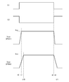
- FIG. 5 is a diagram showing an example of a change in the output voltage Vout of the IPS 21.
- the “H” level instruction signal Sb for turning on the “switch X1” is input at the time t0.
- the "H” level instruction signal Sc for turning off the "switch X1” is input. Therefore, before time t0, the NMOS transistors M1 and M2 (“switch X1”) are turned off by the NMOS transistors 120 of the discharge circuit 74 of FIG. 2 and the switches 121 and 122 that are turned on.
- the charge pump circuit 72 outputs a voltage Vcp and switches 121. , 122 are off.
- the separation circuit 73 applies a voltage corresponding to the voltage Vcp to each of the gate lines L3 and L4.
- the voltage of the source electrode S1 of the NMOS transistor M1 is the power supply voltage Vcc
- the voltage of the source electrode S2 of the NMOS transistor M2 is the ground voltage Vgnd (0V). Therefore, of the NMOS transistors M1 and M2, the NMOS transistor M2 is turned on first.
- the current value at which the NMOS transistor 120 discharges the gate capacitance of the NMOS transistor M1 is set to a sufficiently small value so as not to affect when the NMOS transistor M1 is turned on. ..
- the switches 121 and 122 are switches having a sufficiently small on-resistance. Therefore, the gate capacitance of the NMOS transistor M2 is discharged in a short time via the switches 121 and 122, and the NMOS transistor M2 is immediately turned off. Then, when the NMOS transistor M2 is turned off, the power supply voltage Vcc is cut off by the diode 61. As a result, for example, at time t3, the output voltage Vout drops to the ground voltage.
- the NMOS transistor M1 is in the ON state, but when the NMOS transistor M2 is turned off, the "switch X1" provided between the terminal VCS and the terminal OUT is turned off.
- the NMOS transistors M1 and M2 constituting the "switch X1" are driven by electrically separated gate lines L3 and L4, respectively.
- the time of change of the output voltage Vout is compared between the case of using the "switch X1" having such a configuration and the case of using the "switch” composed of two NMOS transistors having a common gate electrode. ..
- FIG. 6 is a diagram showing an example of the configuration of the IPS 25 according to the comparative example.
- the IPS 25 includes an IC 55 on which a switch (described later) is formed, and an IC 56 having a circuit for turning the switch on and off.
- IPS 21 of FIG. 2 and IPS 25 of FIG. 6 the elements and blocks with the same reference numerals are the same.
- the IC55 includes the NMOS transistors M1 and M2 like the IC50. However, the gate electrodes G1 and G2 of the NMOS transistors M1 and M2 are connected to each other. In the IC55, the connections of the electrodes other than the gate electrodes G1 and G2 of the NMOS transistors M1 and M2 are the same as those of the IC50.
- the switch composed of the NMOS transistors M1 and M2 will be referred to as "switch X2".
- the IC 56 is a circuit for turning on or off the "switch X2", and includes a power supply circuit 70, a control circuit 71, a charge pump circuit 72, a discharge circuit 77, and a resistor 85.
- the power supply circuit 70, the control circuit 71, and the charge pump circuit 72 of the IC 56 are the same as the blocks included in the IC 51, the discharge circuit 77 and the resistor 85 will be described.
- the discharge circuit 77 is a circuit for turning off the NMOS transistors M1 and M2 constituting the "switch X2", and includes switches 125 and 126.
- the switch 125 is provided between the gate line L6 connected to the gate electrodes of the NMOS transistors M1 and M2 and the ground line L5 connected to the terminal GND, and the switch 126 is provided with the gate line L6 and the load line L2. It is provided between.
- the switches 125 and 126 are turned on based on, for example, the instruction signal Sc for turning off the "switch X2". Therefore, the gate capacitance of the NMOS transistors M1 and M2 is discharged via the path of the gate line L6, the switch 125, and the ground line L5, and the path of the gate line L6, the switch 126, and the load line L2.
- the resistor 85 is a gate resistance of the NMOS transistors M1 and M2, and has, for example, the same resistance value as the gate resistance of the NMOS transistors M1 and M2 of IPS21 in FIG.
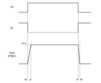
- FIG. 7 is a diagram showing an example of a change in the output voltage Vout of the IPS 25.
- the waveform of the output voltage Vout of the IPS 21 shown in FIG. 5 is shown as a comparison target.
- the charge pump circuit 72 outputs a voltage Vcp and switches 125. , 126 are off.
- the charge pump circuit 72 When the charge pump circuit 72 outputs the voltage Vcp, the voltage Vcp is applied to the gate line L6.
- the charge pump circuit 72 needs to drive a larger capacitance than the “switch X1” of the IPS 21.
- the "switch X2" is turned on at a time t10 later than the time t1 when the above-mentioned "switch X1" is turned on, and the output voltage Vout rises to the power supply voltage Vcc.
- the IPS 21 can turn on the "switch X1" in a shorter period.
- the charge pump circuit 72 stops the output of the voltage Vcp. Then, the switches 125 and 126 are turned on.
- the switches 121 and 122 discharge the gate capacitance of only the NMOS transistors M2, but the switches 125 and 126 of the IPS 25 of FIG. 6 discharge the gate capacitance of the NMOS transistors M1 and M2.
- the "switch X2" is turned off and the output voltage Vout drops to the ground voltage.
- the IPS 21 can turn off the "switch X1" in a shorter period.
- FIG. 8 is a diagram for explaining the operation of the IPS 21 when the battery 11 is reversely connected. For convenience, FIG. 8 shows only a part of the blocks related to the reverse connection operation among the plurality of blocks of the IPS 21 of FIG.
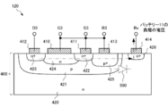
- FIG. 9 is a diagram showing a cross section of the NMOS transistor 120.
- the NMOS transistor 120 includes a gate electrode 410, a source electrode 411, a drain electrode 412, and a substrate electrode 413, 414 formed on the semiconductor substrate 400 of the IC 51 and made of a conductive material such as polysilicon.
- the electrodes of the NMOS transistor 120 are designated by different reference numerals for convenience, but the gate electrode 410 of the NMOS transistor 120 corresponds to the “gate electrode G3” and is a source electrode. 411 corresponds to the “source electrode S3”. Further, the drain electrode 412 corresponds to the “drain electrode D3”, and the substrate electrodes 413 and 414 correspond to the "board electrode B3" and the "board electrode Bx", respectively.
- An n + type contact region 426 is formed inside the semiconductor substrate 400.
- the drift region 420 is a region containing n-type impurities such as phosphorus, and the well region 421 is a p-type region formed on the surface side of the drift region 420.
- the drift region 420 corresponds to the "first region”
- the well region 421 corresponds to the "second region”.
- the source region 422 and the drain region 423 are n + type regions formed in a part of the well region 421, and an n-type gate region 424 is formed between the source region 422 and the drain region 423. Has been done.
- a contact region 425 containing a high concentration of p-type impurities is formed from the well region 421.
- a diode 500 which is a parasitic diode, is formed between the p-type well region 421 and the n-type drift region 420.
- a contact region 426 containing a high concentration of n-type impurities is formed on the surface side of the semiconductor substrate 400 of the n-type drift region 420.
- the power supply voltage Vcc applied to the terminal OUT is applied to the source electrode S3, the gate electrode G3, and the substrate electrode B3 of the NMOS transistor 120 via the motor coil (not shown) of the motor 12, the load line L2, and the like. It is applied.
- the substrate electrode Bx of the n-type semiconductor substrate 400 is usually a terminal so that the power supply voltage Vcc, which is the highest potential, is applied. It is connected to the power supply line L1 of the VCS.
- the voltage of the negative electrode of the battery 11 is applied to the substrate electrode Bx, so that the diode 500, which is the parasitic diode shown in FIG. 9, is turned on.
- the voltage of the source electrode S3, the gate electrode G3, and the substrate electrode B3 of the NMOS transistor 120 drops from the power supply voltage Vcc to the “forward voltage Vfx” of the diode 500.
- the gate capacitance of the NMOS transistor M1 is the gate line L3, the drain electrode D3 of the NMOS transistor 120, the diode 500, and the substrate electrode B3. Is discharged via.
- the path through which the gate capacitance of the NMOS transistor M1 is discharged is shown by a alternate long and short dash line.
- the threshold voltage of the NMOS transistor M1 is set higher than the “forward voltage Vfx” of the diode 500. Therefore, the gate of the NMOS transistor M1 is discharged in such a path, so that the NMOS transistor M1 is surely turned off.
- the power supply voltage Vcc applied to the terminal OUT is output to the NMOS transistor M1 via the diode 61, but is cut off by the MOSFET transistor M1 that is turned off.
- the IPS 21 can appropriately protect the motor 12 and the like even when the battery 11 is reversely connected.
- the voltage Vcp is applied to the gate line L3 via the diodes 100 and 101, and is applied to the gate line L4 via the diodes 102 and 103. Therefore, the voltage Vcp output from one charge pump circuit 72 can be electrically separated and applied to the gate lines L3 and L4.
- a charge pump circuit may be provided for each of the gate lines L3 and L4, but such a configuration increases the circuit scale.
- a voltage can be applied to the electrically separated gate lines L3 and L4 while keeping the circuit scale small.
- the diodes 130 and 131 of the present embodiment can prevent the voltage of the source electrode S1 from becoming too high with respect to the gate electrode G1 of the NMOS transistor M1, the gate oxide film of the NMOS transistor M1 is damaged. Can be suppressed. Further, the diodes 130 and 131 have the effect of precharging the gate capacitance of the gate electrode G1 of the NMOS transistor M1 before the switch X1 is turned on.
- the diodes 132 and 133 of the present embodiment can prevent the voltage of the source electrode S2 from becoming too high with respect to the gate electrode G2 of the NMOS transistor M2, the gate oxide film of the NMOS transistor M2 is damaged. Can be suppressed.
- the discharge circuit 74 discharges the gate capacitance of the NMOS transistor M2 based on the instruction signal Sc, the NMOS transistor M2 is surely turned off.
- the switch 121 of the discharge circuit 74 discharges the gate capacitance of the NMOS transistor M2 to the ground line L5. Therefore, for example, the period for turning off the NMOS transistor M2 can be shortened as compared with the case where only the switch 121 is used.
- gate lines L3 and L4 are provided with resistors 80 and 81, noise when the NMOS transistors M1 and M2 are turned on is suppressed.
- the gate capacitance of the NMOS transistor M1 is discharged by the depletion type NMOS transistor 120.
- the NMOS transistor 120 can surely turn off the NMOS transistor M1 without using a complicated circuit.
- the NMOS transistor 120 is formed in, for example, the p-type well region 421 formed in the n-type drift region 420. In such a configuration, when the battery 11 is reversely connected, the parasitic diode 500 of the NMOS transistor 120 is turned on. As a result, the gate capacitance of the NMOS transistor M1 can be discharged.
- the threshold voltage of the NMOS transistor M1 is larger than the “forward voltage Vfx” of the diode 500. Therefore, when the gate capacitance of the NMOS transistor M1 is discharged via the diode 500, the NMOS transistor M1 is surely turned off. As a result, the IPS 21 can reliably protect the load even when the battery 11 is reversely connected.
- the output voltage Vout of the IPS 21 is applied to the motor 12, which is a load, via the switch 31 of the ECU 20, but the present invention is not limited to this.
- the output voltage Vout of the IPS 21 may be applied directly to the motor 12.
- the IC 51 is an n-type semiconductor substrate, it may be, for example, a p-type semiconductor substrate. Further, when a p-type semiconductor substrate is used for the IC 51, the same effect as that of the present embodiment can be obtained by using a semiconductor device having a twin-well or triple-well structure so that a parasitic diode 500 is formed on the NMOS transistor 120. Can be obtained.
Landscapes
- Engineering & Computer Science (AREA)
- Power Engineering (AREA)
- Manufacturing & Machinery (AREA)
- Chemical & Material Sciences (AREA)
- Chemical Kinetics & Catalysis (AREA)
- Electrochemistry (AREA)
- General Chemical & Material Sciences (AREA)
- Electronic Switches (AREA)
- Semiconductor Integrated Circuits (AREA)
- Power Conversion In General (AREA)
Abstract
Description
この出願は、2019年8月6日に出願された日本特許出願、特願2019-144555に基づく優先権を主張し、その内容を援用する。
図1は、本発明の一実施形態であるモータ制御装置10の構成を示す図である。モータ制御装置10は、バッテリー11からの電力を用いて、自動車に設けられたモータ12を制御するための装置であり、IPS(Intelligent Power Switch)21を含むECU20を有する。なお、バッテリー11は、例えば、自動車用のリチウムイオン電池であり、12Vの電源電圧Vccを出力する。
図2は、IPS21の構成の一例を示す図である。IPS21は、スイッチ(後述)が形成されたIC(Integrated Circuit)50と、スイッチをオン、オフするための回路を有するIC51と、を含んで構成される。
IC50は、電源電圧Vccを、端子OUTから出力させるか否かを切り替えるためのスイッチ(以下、“スイッチX1”と称する。)を構成する2つのMOSトランジスタを含む。とりわけ、本実施形態では、2つのトランジスタはNMOSトランジスタM1,M2である。
図3は、NMOSトランジスタM1,M2の断面を示す図である。NMOSトランジスタM1,M2は、IC50の半導体基板200に形成されている。
図2のIC51は、指示信号Saに基づいて、“スイッチX1”をオン、オフする回路であり、電源回路70、制御回路71、チャージポンプ回路72、分離回路73、放電回路74、ゲート保護回路75,76、及び抵抗80~82を含んで構成される。
図4は、チャージポンプ回路72の一例を示す図である。チャージポンプ回路72は、発振器300、インバータ310,311、ダイオード320~323、及びコンデンサ330,331を含んで構成される。なお、ここでは、ダイオード320~323の順方向電圧を、“Vf”とする。
ここで、クロック信号CLKがハイレベル(以下、“H”レベル)であると、インバータ310の出力がローレベル(以下、“L”レベル)となり、コンデンサ330の一端の電圧Vc1は、ダイオード320を介して充電される。この結果、コンデンサ330の一端の電圧Vc1の電圧は、式(1)で表される。
そして、クロック信号がLレベルになると、インバータ310の出力はHレベル(電源電圧Vdd)となるため、コンデンサ330の一端の電圧Vc1は、式(2)で表される。
また、このタイミングにおいて、インバータ311の出力はLレベルであるため、コンデンサ331の他端は、接地電圧Vgnd(0V)となる。この結果、コンデンサ331の一端の電圧Vc2は、式(3)で表される。
さらに、クロック信号CLKがHレベルになると、インバータ311の出力はHレベルとなるため、コンデンサ331の一端の電圧Vc2は、式(4)で表される。
そして、ダイオード323のカソードには、分離回路73が接続されているため、ダイオード323から出力される電圧Vcpは、式(5)で表される。
なお、本実施形態のチャージポンプ回路72は、2段の昇圧回路を含むこととしたが、これに限られず、電圧VcpがNMOSトランジスタM1,M2をオンできる電圧であれば、どの様な構成であっても良い。
ここで、図1のモータ制御装置10において、IPS21の“スイッチX1”がオン、オフした際の出力電圧Voutについて説明する。なお、ここでは、バッテリー11は、正常な向きに接続されているため、端子VCCには、電源電圧Vccが印加され、端子OUTには、モータ12のコイル(不図示)を介して接地電圧が印加されている。また、チャージポンプ回路72では、十分短い時間で所望の電圧Vcpを生成するよう、クロック信号CLKの周期は設定されていることとする。
図6は、比較例に係るIPS25の構成の一例を示す図である。IPS25は、IPS21と同様に、スイッチ(後述)が形成されたIC55と、スイッチをオン、オフするための回路を有するIC56と、を含んで構成される。なお、図2のIPS21と、図6のIPS25において、同じ符号の付された素子、ブロックは同じである。
図7は、IPS25の出力電圧Voutの変化の一例を示す図である。なお、ここでは、図5で示したIPS21の出力電圧Voutの波形を比較対象として図示している。
図8は、バッテリー11が逆接続された際のIPS21の動作を説明するため図である。なお、便宜上、図8においては、図2のIPS21の複数のブロックうち、逆接続の動作に関連する一部のブロックのみ図示している。
以上、本実施形態のモータ制御装置10について説明した。本実施形態では、“スイッチX1”を構成するNMOSトランジスタM1,M2のゲートラインL3,L4は、電気的に分離されている。このため、例えば、図7に示したように、“スイッチX1”のスイッチング期間は短くなる。
11 バッテリー
12 モータ
20 ECU
21,25 IPS
50,51,55,56 IC
60,61,100~103,130~133,320~323,500 ダイオード
70 電源回路
71 制御回路
72 チャージポンプ回路
73 分離回路
74,77 放電回路
75,76 ゲート保護回路
80~82,85,104,105,134 抵抗
120,M1,M2 NMOSトランジスタ
121,122,125,126 スイッチ
200,400 半導体基板
220,420 ドリフト領域
222,421 ウェル領域
223,422 ソース領域
221,423 ドレイン領域
224,425,426 コンタクト領域
230 ゲートトレンチ部
231 酸化膜
240 絶縁膜
300 発振器
310,311 インバータ
330,331 コンデンサ
G1~G3,241,410 ゲート電極
S1~S3,211,411 ソース電極
D1~D3,210,412 ドレイン電極
B3,Bx,212,413,414 基板電極
424 ゲート領域
Claims (11)
- 電源電圧が印加される第1ラインと負荷が接続される第2ラインとの間で互いのドレイン電極が直列に接続された第1及び第2MOSトランジスタと、
前記第1MOSトランジスタのゲート電極に接続された第3ラインと、
前記第2MOSトランジスタのゲート電極に接続され、前記第3ラインと電気的に分離して設けられた第4ラインと、
を備えることを特徴とする半導体装置。 - 請求項1に記載の半導体装置であって、
前記第1及び第2MOSトランジスタをオンするための所定電圧を、前記第3ラインに印加する第1ダイオードと、
前記所定電圧を、前記第4ラインに印加する第2ダイオードと、
を備えることを特徴とする半導体装置。 - 請求項2に記載の半導体装置であって、
前記第1及び第2MOSトランジスタのオンを指示する第1指示信号に基づいて、前記第1及び第2ダイオードに前記所定電圧を出力するチャージポンプ回路を備えること、
を特徴とする半導体装置。 - 請求項1~3の何れか一項に記載の半導体装置であって、
アノード側が前記第1ラインに接続され、カソード側が前記第3ラインに接続された第3ダイオードを備えること、
を特徴とする半導体装置。 - 請求項1~4の何れか一項に記載の半導体装置であって、
アノード側が前記第2ラインに接続され、カソード側が前記第4ラインに接続された第4ダイオードを備えること、
を特徴とする半導体装置。 - 請求項1~5の何れか一項に記載の半導体装置であって、
前記第2MOSトランジスタのオフを指示する第2指示信号に基づいて、前記第2MOSトランジスタのゲート容量を放電する放電回路を備えること、
を特徴とする半導体装置。 - 請求項6に記載の半導体装置であって、
前記放電回路は、
前記第4ラインと、接地側の第5ラインとの間に設けられ、前記第2指示信号に基づいてオンする第1スイッチと、
前記第4ラインと、前記第2ラインとの間に設けられ、前記第2指示信号に基づいてオンする第2スイッチと、
を含むこと、
を特徴とする半導体装置。 - 請求項1~7の何れか一項に記載の半導体装置であって、
前記第3ラインと、前記第4ラインとにそれぞれ、抵抗が設けられていること、
を特徴とする半導体装置。 - 請求項1~8の何れか一項に記載の半導体装置であって、
デプレッション型の第3MOSトランジスタを備え、
前記第3MOSトランジスタは、ゲート電極とソース電極とが前記第2ラインに接続され、ドレイン電極が前記第3ラインに接続されること、
を特徴とする半導体装置。 - 請求項9に記載の半導体装置であって、
前記第3MOSトランジスタは、NMOSトランジスタであって、半導体基板のn型の第1領域に形成されたp型の第2領域に形成されていること、
を特徴とする半導体装置。 - 請求項10に記載の半導体装置であって、
前記第1MOSトランジスタの閾値電圧は、前記第1及び第2領域で形成される寄生ダイオードの順方向電圧より大きいこと、
を特徴とする半導体装置。
Priority Applications (3)
| Application Number | Priority Date | Filing Date | Title |
|---|---|---|---|
| JP2021537620A JP7099640B2 (ja) | 2019-08-06 | 2020-06-26 | 半導体装置 |
| CN202080011324.9A CN113396541B (zh) | 2019-08-06 | 2020-06-26 | 半导体装置 |
| US17/381,426 US12230627B2 (en) | 2019-08-06 | 2021-07-21 | Semiconductor device |
Applications Claiming Priority (2)
| Application Number | Priority Date | Filing Date | Title |
|---|---|---|---|
| JP2019-144555 | 2019-08-06 | ||
| JP2019144555 | 2019-08-06 |
Related Child Applications (1)
| Application Number | Title | Priority Date | Filing Date |
|---|---|---|---|
| US17/381,426 Continuation US12230627B2 (en) | 2019-08-06 | 2021-07-21 | Semiconductor device |
Publications (1)
| Publication Number | Publication Date |
|---|---|
| WO2021024643A1 true WO2021024643A1 (ja) | 2021-02-11 |
Family
ID=74502920
Family Applications (1)
| Application Number | Title | Priority Date | Filing Date |
|---|---|---|---|
| PCT/JP2020/025212 Ceased WO2021024643A1 (ja) | 2019-08-06 | 2020-06-26 | 半導体装置 |
Country Status (4)
| Country | Link |
|---|---|
| US (1) | US12230627B2 (ja) |
| JP (1) | JP7099640B2 (ja) |
| CN (1) | CN113396541B (ja) |
| WO (1) | WO2021024643A1 (ja) |
Cited By (1)
| Publication number | Priority date | Publication date | Assignee | Title |
|---|---|---|---|---|
| US12218654B2 (en) | 2022-09-26 | 2025-02-04 | Kabushiki Kaisha Toshiba | Switching device |
Families Citing this family (2)
| Publication number | Priority date | Publication date | Assignee | Title |
|---|---|---|---|---|
| JP7549002B2 (ja) * | 2021-12-31 | 2024-09-10 | イノサイエンス (スーチョウ) セミコンダクター カンパニー リミテッド | 窒化物系双方向スイッチング装置とその製造方法 |
| CN116317623A (zh) * | 2023-04-27 | 2023-06-23 | 元山(济南)电子科技有限公司 | 一种场效应管控制电路和桥式变换器 |
Citations (6)
| Publication number | Priority date | Publication date | Assignee | Title |
|---|---|---|---|---|
| JPS5154778A (ja) * | 1974-11-08 | 1976-05-14 | Fujitsu Ltd | |
| JPS5181578A (ja) * | 1975-01-16 | 1976-07-16 | Hitachi Ltd | Handotaisochi |
| JPH0463475A (ja) * | 1990-07-03 | 1992-02-28 | Toshiba Corp | 半導体装置 |
| JPH06348350A (ja) * | 1993-06-10 | 1994-12-22 | Matsushita Electric Works Ltd | 電源装置 |
| JPH11178224A (ja) * | 1997-12-08 | 1999-07-02 | Nec Kansai Ltd | 電池パック |
| JP2013150139A (ja) * | 2012-01-19 | 2013-08-01 | Asahi Kasei Electronics Co Ltd | 電源接続装置 |
Family Cites Families (9)
| Publication number | Priority date | Publication date | Assignee | Title |
|---|---|---|---|---|
| JPS5530312B2 (ja) | 1975-01-16 | 1980-08-09 | ||
| US5539610A (en) | 1993-05-26 | 1996-07-23 | Siliconix Incorporated | Floating drive technique for reverse battery protection |
| JP2001224135A (ja) | 2000-02-08 | 2001-08-17 | Nissan Motor Co Ltd | 負荷駆動装置 |
| JP4942007B2 (ja) | 2004-10-25 | 2012-05-30 | ルネサスエレクトロニクス株式会社 | 半導体集積回路 |
| JP2006217699A (ja) | 2005-02-02 | 2006-08-17 | Yazaki Corp | 異常検出装置 |
| JP5747727B2 (ja) | 2011-08-08 | 2015-07-15 | 株式会社デンソー | 電源逆接保護装置 |
| JP5488550B2 (ja) * | 2011-08-19 | 2014-05-14 | 株式会社安川電機 | ゲート駆動回路および電力変換装置 |
| JP6229952B2 (ja) * | 2012-08-10 | 2017-11-15 | パナソニックIpマネジメント株式会社 | バッテリー装置およびバッテリー制御装置 |
| JP6117640B2 (ja) * | 2013-07-19 | 2017-04-19 | ルネサスエレクトロニクス株式会社 | 半導体装置及び駆動システム |
-
2020
- 2020-06-26 WO PCT/JP2020/025212 patent/WO2021024643A1/ja not_active Ceased
- 2020-06-26 JP JP2021537620A patent/JP7099640B2/ja active Active
- 2020-06-26 CN CN202080011324.9A patent/CN113396541B/zh active Active
-
2021
- 2021-07-21 US US17/381,426 patent/US12230627B2/en active Active
Patent Citations (6)
| Publication number | Priority date | Publication date | Assignee | Title |
|---|---|---|---|---|
| JPS5154778A (ja) * | 1974-11-08 | 1976-05-14 | Fujitsu Ltd | |
| JPS5181578A (ja) * | 1975-01-16 | 1976-07-16 | Hitachi Ltd | Handotaisochi |
| JPH0463475A (ja) * | 1990-07-03 | 1992-02-28 | Toshiba Corp | 半導体装置 |
| JPH06348350A (ja) * | 1993-06-10 | 1994-12-22 | Matsushita Electric Works Ltd | 電源装置 |
| JPH11178224A (ja) * | 1997-12-08 | 1999-07-02 | Nec Kansai Ltd | 電池パック |
| JP2013150139A (ja) * | 2012-01-19 | 2013-08-01 | Asahi Kasei Electronics Co Ltd | 電源接続装置 |
Cited By (1)
| Publication number | Priority date | Publication date | Assignee | Title |
|---|---|---|---|---|
| US12218654B2 (en) | 2022-09-26 | 2025-02-04 | Kabushiki Kaisha Toshiba | Switching device |
Also Published As
| Publication number | Publication date |
|---|---|
| JP7099640B2 (ja) | 2022-07-12 |
| CN113396541A (zh) | 2021-09-14 |
| JPWO2021024643A1 (ja) | 2021-11-25 |
| US12230627B2 (en) | 2025-02-18 |
| CN113396541B (zh) | 2025-06-10 |
| US20210351177A1 (en) | 2021-11-11 |
Similar Documents
| Publication | Publication Date | Title |
|---|---|---|
| US5917359A (en) | Semiconductor apparatus having protective circuitry | |
| US7495482B2 (en) | Semiconductor device | |
| US7466189B2 (en) | Semiconductor integrated circuit | |
| US10096705B2 (en) | Integrated high side gate driver structure and circuit for driving high side power transistors | |
| CN100446419C (zh) | 半导体器件 | |
| US20090315595A1 (en) | Output drive circuit | |
| JP7099640B2 (ja) | 半導体装置 | |
| JP2011139403A (ja) | 電力供給制御回路 | |
| CN112821728B (zh) | 开关控制电路、半导体装置 | |
| US6844769B2 (en) | Drive circuit | |
| US7606082B2 (en) | Semiconductor circuit, inverter circuit, semiconductor apparatus, and manufacturing method thereof | |
| JP7505267B2 (ja) | スイッチング制御回路、半導体装置 | |
| US20080169863A1 (en) | Semiconductor integrated circuit device including charge pump circuit capable of suppressing noise | |
| JP2000286687A (ja) | レベルシフト回路及びインバータ装置 | |
| JP7533109B2 (ja) | 半導体装置 | |
| JP3617425B2 (ja) | 半導体集積回路装置の入力インターフェイス回路 | |
| JP5805573B2 (ja) | 出力回路 | |
| JP2021150532A (ja) | 半導体装置 | |
| JP2007281196A (ja) | 半導体装置 | |
| JP3518310B2 (ja) | 容量性負荷駆動回路 | |
| JP7581763B2 (ja) | 半導体装置 | |
| JP5226474B2 (ja) | 半導体出力回路 | |
| KR101091835B1 (ko) | 음전압 공급장치 | |
| JP2990998B2 (ja) | 半導体装置及びその製造方法 | |
| JP3396872B2 (ja) | 電圧検出回路及び高電圧出力回路 |
Legal Events
| Date | Code | Title | Description |
|---|---|---|---|
| 121 | Ep: the epo has been informed by wipo that ep was designated in this application |
Ref document number: 20849247 Country of ref document: EP Kind code of ref document: A1 |
|
| ENP | Entry into the national phase |
Ref document number: 2021537620 Country of ref document: JP Kind code of ref document: A |
|
| NENP | Non-entry into the national phase |
Ref country code: DE |
|
| 122 | Ep: pct application non-entry in european phase |
Ref document number: 20849247 Country of ref document: EP Kind code of ref document: A1 |
|
| WWG | Wipo information: grant in national office |
Ref document number: 202080011324.9 Country of ref document: CN |