WO2021020378A1 - 発光素子及び発光素子の製造方法 - Google Patents
発光素子及び発光素子の製造方法 Download PDFInfo
- Publication number
- WO2021020378A1 WO2021020378A1 PCT/JP2020/028840 JP2020028840W WO2021020378A1 WO 2021020378 A1 WO2021020378 A1 WO 2021020378A1 JP 2020028840 W JP2020028840 W JP 2020028840W WO 2021020378 A1 WO2021020378 A1 WO 2021020378A1
- Authority
- WO
- WIPO (PCT)
- Prior art keywords
- light
- wavelength
- active layer
- light emitting
- emitting element
- Prior art date
- Legal status (The legal status is an assumption and is not a legal conclusion. Google has not performed a legal analysis and makes no representation as to the accuracy of the status listed.)
- Ceased
Links
Images

Classifications
-
- H—ELECTRICITY
- H10—SEMICONDUCTOR DEVICES; ELECTRIC SOLID-STATE DEVICES NOT OTHERWISE PROVIDED FOR
- H10H—INORGANIC LIGHT-EMITTING SEMICONDUCTOR DEVICES HAVING POTENTIAL BARRIERS
- H10H29/00—Integrated devices, or assemblies of multiple devices, comprising at least one light-emitting semiconductor element covered by group H10H20/00
- H10H29/10—Integrated devices comprising at least one light-emitting semiconductor component covered by group H10H20/00
-
- H—ELECTRICITY
- H10—SEMICONDUCTOR DEVICES; ELECTRIC SOLID-STATE DEVICES NOT OTHERWISE PROVIDED FOR
- H10H—INORGANIC LIGHT-EMITTING SEMICONDUCTOR DEVICES HAVING POTENTIAL BARRIERS
- H10H20/00—Individual inorganic light-emitting semiconductor devices having potential barriers, e.g. light-emitting diodes [LED]
- H10H20/80—Constructional details
- H10H20/81—Bodies
- H10H20/814—Bodies having reflecting means, e.g. semiconductor Bragg reflectors
-
- H—ELECTRICITY
- H10—SEMICONDUCTOR DEVICES; ELECTRIC SOLID-STATE DEVICES NOT OTHERWISE PROVIDED FOR
- H10H—INORGANIC LIGHT-EMITTING SEMICONDUCTOR DEVICES HAVING POTENTIAL BARRIERS
- H10H20/00—Individual inorganic light-emitting semiconductor devices having potential barriers, e.g. light-emitting diodes [LED]
- H10H20/01—Manufacture or treatment
- H10H20/011—Manufacture or treatment of bodies, e.g. forming semiconductor layers
- H10H20/013—Manufacture or treatment of bodies, e.g. forming semiconductor layers having light-emitting regions comprising only Group III-V materials
- H10H20/0137—Manufacture or treatment of bodies, e.g. forming semiconductor layers having light-emitting regions comprising only Group III-V materials the light-emitting regions comprising nitride materials
-
- H—ELECTRICITY
- H10—SEMICONDUCTOR DEVICES; ELECTRIC SOLID-STATE DEVICES NOT OTHERWISE PROVIDED FOR
- H10H—INORGANIC LIGHT-EMITTING SEMICONDUCTOR DEVICES HAVING POTENTIAL BARRIERS
- H10H20/00—Individual inorganic light-emitting semiconductor devices having potential barriers, e.g. light-emitting diodes [LED]
- H10H20/80—Constructional details
- H10H20/81—Bodies
- H10H20/813—Bodies having a plurality of light-emitting regions, e.g. multi-junction LEDs or light-emitting devices having photoluminescent regions within the bodies
-
- H—ELECTRICITY
- H10—SEMICONDUCTOR DEVICES; ELECTRIC SOLID-STATE DEVICES NOT OTHERWISE PROVIDED FOR
- H10H—INORGANIC LIGHT-EMITTING SEMICONDUCTOR DEVICES HAVING POTENTIAL BARRIERS
- H10H20/00—Individual inorganic light-emitting semiconductor devices having potential barriers, e.g. light-emitting diodes [LED]
- H10H20/80—Constructional details
- H10H20/81—Bodies
- H10H20/814—Bodies having reflecting means, e.g. semiconductor Bragg reflectors
- H10H20/8142—Bodies having reflecting means, e.g. semiconductor Bragg reflectors forming resonant cavity structures
-
- H—ELECTRICITY
- H10—SEMICONDUCTOR DEVICES; ELECTRIC SOLID-STATE DEVICES NOT OTHERWISE PROVIDED FOR
- H10H—INORGANIC LIGHT-EMITTING SEMICONDUCTOR DEVICES HAVING POTENTIAL BARRIERS
- H10H20/00—Individual inorganic light-emitting semiconductor devices having potential barriers, e.g. light-emitting diodes [LED]
- H10H20/80—Constructional details
- H10H20/84—Coatings, e.g. passivation layers or antireflective coatings
- H10H20/841—Reflective coatings, e.g. dielectric Bragg reflectors
-
- H—ELECTRICITY
- H10—SEMICONDUCTOR DEVICES; ELECTRIC SOLID-STATE DEVICES NOT OTHERWISE PROVIDED FOR
- H10H—INORGANIC LIGHT-EMITTING SEMICONDUCTOR DEVICES HAVING POTENTIAL BARRIERS
- H10H20/00—Individual inorganic light-emitting semiconductor devices having potential barriers, e.g. light-emitting diodes [LED]
- H10H20/80—Constructional details
- H10H20/85—Packages
- H10H20/851—Wavelength conversion means
- H10H20/8511—Wavelength conversion means characterised by their material, e.g. binder
- H10H20/8512—Wavelength conversion materials
-
- H—ELECTRICITY
- H10—SEMICONDUCTOR DEVICES; ELECTRIC SOLID-STATE DEVICES NOT OTHERWISE PROVIDED FOR
- H10H—INORGANIC LIGHT-EMITTING SEMICONDUCTOR DEVICES HAVING POTENTIAL BARRIERS
- H10H20/00—Individual inorganic light-emitting semiconductor devices having potential barriers, e.g. light-emitting diodes [LED]
- H10H20/80—Constructional details
- H10H20/862—Resonant cavity structures
-
- H—ELECTRICITY
- H10—SEMICONDUCTOR DEVICES; ELECTRIC SOLID-STATE DEVICES NOT OTHERWISE PROVIDED FOR
- H10H—INORGANIC LIGHT-EMITTING SEMICONDUCTOR DEVICES HAVING POTENTIAL BARRIERS
- H10H20/00—Individual inorganic light-emitting semiconductor devices having potential barriers, e.g. light-emitting diodes [LED]
- H10H20/01—Manufacture or treatment
- H10H20/034—Manufacture or treatment of coatings
-
- H—ELECTRICITY
- H10—SEMICONDUCTOR DEVICES; ELECTRIC SOLID-STATE DEVICES NOT OTHERWISE PROVIDED FOR
- H10H—INORGANIC LIGHT-EMITTING SEMICONDUCTOR DEVICES HAVING POTENTIAL BARRIERS
- H10H20/00—Individual inorganic light-emitting semiconductor devices having potential barriers, e.g. light-emitting diodes [LED]
- H10H20/01—Manufacture or treatment
- H10H20/036—Manufacture or treatment of packages
- H10H20/0361—Manufacture or treatment of packages of wavelength conversion means
-
- H—ELECTRICITY
- H10—SEMICONDUCTOR DEVICES; ELECTRIC SOLID-STATE DEVICES NOT OTHERWISE PROVIDED FOR
- H10H—INORGANIC LIGHT-EMITTING SEMICONDUCTOR DEVICES HAVING POTENTIAL BARRIERS
- H10H20/00—Individual inorganic light-emitting semiconductor devices having potential barriers, e.g. light-emitting diodes [LED]
- H10H20/80—Constructional details
- H10H20/81—Bodies
- H10H20/811—Bodies having quantum effect structures or superlattices, e.g. tunnel junctions
- H10H20/812—Bodies having quantum effect structures or superlattices, e.g. tunnel junctions within the light-emitting regions, e.g. having quantum confinement structures
-
- H—ELECTRICITY
- H10—SEMICONDUCTOR DEVICES; ELECTRIC SOLID-STATE DEVICES NOT OTHERWISE PROVIDED FOR
- H10H—INORGANIC LIGHT-EMITTING SEMICONDUCTOR DEVICES HAVING POTENTIAL BARRIERS
- H10H20/00—Individual inorganic light-emitting semiconductor devices having potential barriers, e.g. light-emitting diodes [LED]
- H10H20/80—Constructional details
- H10H20/81—Bodies
- H10H20/822—Materials of the light-emitting regions
- H10H20/824—Materials of the light-emitting regions comprising only Group III-V materials, e.g. GaP
- H10H20/825—Materials of the light-emitting regions comprising only Group III-V materials, e.g. GaP containing nitrogen, e.g. GaN
Definitions
- the present invention relates to a light emitting element and a method for manufacturing the light emitting element.
- Patent Document 1 discloses a technique for forming a plurality of light emitting elements that emit light having different wavelengths on the same wafer. In this technology, by repeating the process of forming a mask other than the necessary part and then forming an active layer for each wavelength multiple times, it is possible to form a plurality of light emitting regions that emit light of different wavelengths adjacent to each other. it can.
- the growth process of the active layer occupies a large proportion of the manufacturing cost of the light emitting device.
- a processing time including installation of a substrate on a crystal growth apparatus, temperature rise to a growth temperature, and the like is required for each growth step, so that the manufacturing cost is significantly increased.
- an object of the present invention is to provide a light emitting element and a method for manufacturing the light emitting element, which can be manufactured by a simpler process.
- the first active layer that emits light of the first wavelength by injecting a current and the first wavelength by absorbing the light of the first wavelength.
- a second active layer that emits light of a second wavelength different from that of the above, and a first reflector whose reflectance of light of the first wavelength is higher than that of light of the second wavelength.
- the first reflecting mirror emits light emitted from the first active layer or the second active layer to the outside rather than the first active layer and the second active layer.
- a light emitting element characterized by being arranged at a position close to the emission end.
- the step of forming the first active layer that emits the light of the first wavelength by injecting a current, and the reflectance of the light of the first wavelength are higher than the reflectance of the light of the second wavelength. It also has a step of forming a high first reflector, wherein the first active layer or the first active layer is more than the first active layer and the second active layer.
- a method for manufacturing a light emitting element characterized in that the light emitted from the active layer 2 is arranged at a position close to an emission end for emitting light to the outside.
- the present invention it is possible to provide a light emitting element that can be manufactured by a simple process and a method for manufacturing the light emitting element.
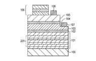
- FIG. 1 is a cross-sectional view schematically showing the structure of the light emitting element according to the present embodiment.
- the first semiconductor layer 101, the second active layer 102, the second semiconductor layer 103, and the first active layer 104 are placed on the substrate 100.
- the third semiconductor layer 105 and the first reflector 106 have a laminated structure arranged in this order. Each of these layers can be formed by epitaxial growth.
- the light emitting element of the present embodiment has a first electrode 107 arranged on the second semiconductor layer 103 and a second electrode 108 arranged on the third semiconductor layer 105.
- the first active layer 104 emits light having a wavelength distribution in which the first wavelength is the main peak when a current is injected.
- "light having a wavelength distribution in which the first wavelength is the main peak” may be simply described as "light having the first wavelength”.
- the second active layer 102 absorbs the light of the first wavelength, it emits the light of the second wavelength different from the first wavelength by photoexcitation.
- the light having the first wavelength can be, for example, blue light having a wavelength of about 450 nm.
- the light of the second wavelength can be, for example, green light having a wavelength of about 525 nm.
- the first active layer 104 and the second active layer 102 may be made of a single layer material, and may be made of a multiple quantum well structure in which a plurality of sets of quantum well layers and barrier layers are alternately laminated. You may. Light of a desired wavelength is obtained by appropriately setting the materials, composition, thickness, number of pairs, etc. of the active layer, quantum well layer, and barrier layer according to the type of the substrate and designing the bandgap so as to obtain a desired band gap. It is possible to realize a light emitting element that emits light. As an example, when the material of the substrate 100 is sapphire and the material of the active layer is InGaN, the central emission wavelength can be changed by changing the proportion of In. As the proportion of In is increased, the central emission wavelength becomes longer.
- the first semiconductor layer 101 is n-type or i-type
- the second semiconductor layer 103 is n-type
- the third semiconductor layer 105 is p-type.
- the first active layer 104 is sandwiched between a first conductive type (n type) semiconductor layer and a second conductive type (p type) semiconductor layer opposite to the first conductive type.
- the second active layer 102 is sandwiched between the first conductive type or i-type semiconductor layer and the first conductive type semiconductor layer.
- the conductive type of the substrate 100 may be any of n-type, p-type and i-type.
- the i-type semiconductor layer refers to a non-doped (undoped) semiconductor layer.
- the non-doping may include both those in which the dopant for controlling the conductive type is not intentionally doped during the growth of the semiconductor layer and those in which approximately the same number of p-type and n-type dopants are doped.
- the carrier concentration in the i-type semiconductor layer is preferably 1 ⁇ 10 16 cm -3 or less.
- each semiconductor layer is composed of GaN and AlGaN-based materials which are group III nitride semiconductors, Si, Ge and the like are used as n-type dopants, and Mg, Zn and the like are used as p-type dopants. Used.
- the group II element Mg, Zn, etc.
- the VI group element Se, etc.
- IV elements C, Si, etc.
- the injection end for emitting light to the outside is on the opposite side to the substrate 100, that is, on the upper side in FIG.
- the first reflector 106 is arranged on the injection end side of the light emitting element.
- the upper surface of the first reflecting mirror 106 is the injection end of the light emitting element.
- the first reflector 106 is designed so that the reflectance of the light of the first wavelength is higher than the reflectance of the light of the second wavelength.
- the first reflector 106 is, for example, a distributed Bragg reflector.
- the distributed Bragg reflector is referred to as a DBR (Distributed Bragg Reflector).
- the DBR is a reflector having a structure in which two thin films having different refractive indexes are alternately and periodically formed so as to have an optical film thickness of 1/4 wavelength.
- the first reflecting mirror 106 may be a plurality of semiconductor layers formed by epitaxial growth, or may be a plurality of dielectric layers. Of these two types of configurations, the configuration using a plurality of dielectric layers is preferable because the difference in refractive index between the two thin films can be increased and a high reflectance can be realized with a small number of pairs. is there.
- the first electrode 107 and the second electrode 108 are given different potentials so that a current can be injected into the first active layer 104.
- the first active layer 104 emits light of a first wavelength.
- the component emitted downward is directly incident on the second active layer 102.
- the light of the first wavelength emitted from the first active layer 104 a part of the components emitted upward is reflected by the first reflecting mirror 106 and incident on the second active layer 102. ..
- the reflectance of the first reflecting mirror 106 is designed to be high with respect to the light of the first wavelength, the light of the first wavelength transmitted through the first reflecting mirror 106 is small. Therefore, most of the light of the first wavelength is incident on the second active layer 102.
- the second active layer 102 absorbs light of the first wavelength and emits light of the second wavelength by photoexcitation. A part of the light of the second wavelength is reflected by the first reflector 106 and returns to the substrate 100 side. However, since the reflectance of the first reflector 106 to the light of the second wavelength is designed to be lower than the reflectance to the light of the first wavelength, most of the light of the second wavelength is the first. It is emitted in the direction perpendicular to the substrate 100 (upper side in FIG. 1) through the reflector 106 of the above. As a result, the light emitting element of the present embodiment can selectively emit light of the second wavelength to the outside.
- the light emitting element of the present embodiment converts light of the first wavelength into light of the second wavelength by using the first active layer 104, the second active layer 102, and the first reflecting mirror 106. , Can be selectively ejected to the outside.
- the first reflecting mirror 106 By arranging the first reflecting mirror 106, the above-mentioned effect can be obtained in a state where the first active layer 104 and the second active layer 102 are laminated in the thickness direction. Therefore, the first active layer 104 It is not necessary to perform patterning between the formation of the active layer 102 and the second active layer 102. Therefore, according to the present embodiment, there is provided a light emitting device capable of forming a plurality of active layers in a simple process.
- the light emitting element of this embodiment is used, for example, as a pixel of a display.
- the display surface of the display can be formed by manufacturing the light emitting elements of the present embodiment in a size of about several tens to several hundreds of ⁇ m and arranging them so as to form a plurality of rows and a plurality of columns.
- a display using an LED (Light Emitting Diode) of an inorganic compound semiconductor in this way is sometimes called a ⁇ LED display.
- the ⁇ LED display is superior to the liquid crystal display and the organic LED display in terms of life, brightness and the like. The effect when the light emitting element of this embodiment is used for the ⁇ LED display will be described.
- the manufacturing method of the ⁇ LED display there is a method of mounting the light emitting elements manufactured for each color such as blue, green, and red on the substrate of the display.
- this method since it is necessary to mount a large number of light emitting elements, there may be a problem that the mounting cost is high. Therefore, in order to reduce the mounting cost, it is desirable to form a plurality of color light emitting elements on the same wafer so that the plurality of light emitting elements can be mounted at once.
- the epitaxial growth process includes time-consuming steps such as mounting the substrate on the crystal growth apparatus and raising the temperature to the growth temperature.
- time-consuming steps such as mounting the substrate on the crystal growth apparatus and raising the temperature to the growth temperature.
- the light emitting element of the present embodiment has a structure capable of performing wavelength conversion in a state where the first active layer 104 and the second active layer 102 are laminated in the thickness direction. Therefore, it is not necessary to perform patterning between the formation of the first active layer 104 and the second active layer 102. Therefore, even if the light emitting elements of two colors are formed on the same wafer, the two active layers can be continuously formed by epitaxial growth. Therefore, in the manufacture of the ⁇ LED display using the light emitting element of the present embodiment, a plurality of active layers can be formed by a simple process, so that the cost can be reduced.
- the two active layers by epitaxial growth, surface contamination due to removal from the crystal growth apparatus or the like is reduced. Therefore, in the production of the light emitting device of the present embodiment, the cleanliness of the growth surface is maintained, so that the effects of improving the yield, stabilizing the production process, and improving the quality of the active layer can also be obtained.
- the light emitting element of this embodiment can be suitably used as a pixel for a ⁇ LED display and its effect have been described above, but the same applies to other embodiments described later.
- the applications of the light emitting elements of this embodiment and other embodiments are not limited to this, and may be applied to applications other than displays such as lighting devices.
- the injection end may be on the side of the substrate 100.
- the structure or material so that the light absorption rate of the substrate 100 is low. Specific examples of the design include using a material having a low absorption rate with respect to the wavelength of the emitted light for the substrate 100, or making the thickness of the substrate 100 sufficiently thin.
- the first active layer 104 is arranged closer to the injection end than the second active layer 102, but the order in which the first active layer 104 and the second active layer 102 are laminated is May be reversed.
- a current is injected into the first active layer 104 at the positions of the first electrode 107 and the second electrode 108. It is necessary to change as appropriate.
- the first active layer 104 is arranged closer to the injection end than the second active layer 102.
- the second active layer 102 is arranged between the first active layer 104 and the substrate 100.
- the contact hole in which the first electrode 107 for current injection is arranged is made shallower as compared with the case where the first active layer 104 and the second active layer 102 are arranged in reverse. There is an advantage that the etching amount can be reduced.
- the semiconductor layer between the first active layer 104 or the second active layer 102 and the substrate 100 is not doped with a p-type dopant.
- Doping a p-type dopant in a semiconductor layer may reduce the crystal quality of the semiconductor layer.
- the quality of the active layer may also deteriorate due to the low crystal quality of the semiconductor layer.
- the active layer is a GaN-based material, the quality of the active layer has a large effect on the light emission characteristics. Therefore, the light emission characteristics can be improved by not doping the p-type dopant under the active layer.
- the first semiconductor layer 101 and the second active layer 102 are n-type or i-type without doping with a p-type dopant, and the second semiconductor layer 103 is a p-type dopant. Is undoped n-type. As a result, it is possible to reduce the deterioration of the quality of the active layer due to the p-type dopant for both the first active layer 104 and the second active layer 102, and the light emitting characteristics are improved.
- FIG. 2 is a cross-sectional view schematically showing the structure of the light emitting element according to the present embodiment.
- the first semiconductor layer 101 includes a second reflector 201.
- the second reflecting mirror 201 is arranged on the opposite side of the first active layer 104 and the second active layer 102 from the first reflecting mirror 106.
- the second reflector 201 like the first reflector 106, is designed so that the reflectance for light of the first wavelength is higher than the reflectance for light of the second wavelength.
- the second reflector 201 is, for example, a DBR.
- the second reflecting mirror 201 may be a DBR having two types of semiconductor layers having different refractive indexes laminated alternately. Examples of two different types of semiconductor layers constituting the DBR include AlGaN, InGaN, and the like.
- the light of the first wavelength emitted from the first active layer 104 is emitted in both the upward direction and the downward direction in FIG.
- a part of the light of the first wavelength emitted downward from the first active layer 104 is absorbed by the second active layer 102.
- the second active layer 102 emits light having a second wavelength by photoexcitation.
- the other part of the light of the first wavelength emitted downward is transmitted without being absorbed by the second active layer 102.
- the light of the first wavelength transmitted through the second active layer 102 is reflected by the second reflecting mirror 201 and re-entered into the second active layer 102 to excite the light of the second wavelength.
- the light of the first wavelength emitted upward from the first active layer 104 is reflected by the first reflecting mirror 106 and is reflected by the first reflecting mirror 106, as in the case of the first embodiment, and is reflected by the second active layer. It is incident on 102 and excites light of a second wavelength.
- the second reflecting mirror 201 is arranged on the opposite side of the first active layer 104 and the second active layer 102 from the first reflecting mirror 106. According to this configuration, the light of the first wavelength emitted downward from the first active layer 104 and transmitted through the second active layer 102 can be returned to the second active layer 102 again. It is possible to improve the conversion efficiency from light of a wavelength to light of a second wavelength. Therefore, the luminous efficiency of the light of the second wavelength is improved. In addition, the leakage of light of the first wavelength can be reduced.
- each layer of the first reflecting mirror 106 and the second reflecting mirror 201 are set so as to form a resonator for the first wavelength.
- the thickness of each layer is such that the reciprocating length of light propagating between the first reflector 106 and the second reflector 201 is an integral multiple of half the first wavelength. Should be set. Thereby, the conversion efficiency from the light of the first wavelength to the light of the second wavelength can be further improved.
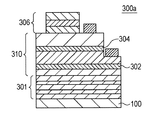
- the light emitting element 300a shown in FIG. 3A is a cross-sectional view showing a model used in the simulation of the configuration corresponding to the present embodiment.
- a GaN / AlInN semiconductor DBR301 (10 pairs)
- a 1 ⁇ resonator 310 composed of GaN
- a SiO 2 / SiN dielectric DBR306 (6 pairs) are arranged in this order on a GaN substrate 100. It has a laminated structure.
- the 1 ⁇ resonator 310 includes a blue quantum well active layer 304 (emission wavelength 450 nm) and a green quantum well active layer 302 (emission wavelength 525 nm).
- the 1 ⁇ resonator 310 is configured to have an optical film thickness of 1 ⁇ (1 wavelength) including the layer thicknesses of these two active layers.
- the design wavelength of each DBR and 1 ⁇ resonator 310 is 450 nm, which is the same as the emission wavelength of the blue quantum well active layer 304.
- the absorption rate of light having a wavelength of 450 nm in the green quantum well active layer 302 is designed so that light having a wavelength of 450 nm is absorbed by 5.8% when it is transmitted from one surface to the other. This design can be made by adjusting the number of quantum wells.
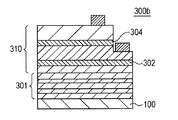
- the light emitting element 300b shown in FIG. 3B is a cross-sectional view showing a model used in the simulation of a comparative example for the present embodiment.
- the light emitting element 300b excludes the SiO 2 / SiN dielectric DBR306 from the configuration of the light emitting element 300a, and is a model that does not form a resonator.
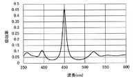
- FIG. 3C is a graph showing a simulation result of the absorption rate in the green quantum well active layer 302 when light is incident on the laminated surface of the semiconductor layer in the direction perpendicular to the laminated surface.
- the vertical axis of FIG. 3C is the absorption rate in the green quantum well active layer 302, and the horizontal axis is the wavelength of the incident light.
- FIG. 3C shows the simulation result by the model of the light emitting element 300a (that is, when there is the SiO 2 / SiN dielectric DBR306). Further, in the simulation of the comparative example using the model of the light emitting element 300b, the absorption rate for light having a wavelength of 450 nm was 0.044.
- FIG. 4 is a graph showing the reflectance characteristics of the SiO 2 / SiN dielectric DBR306 used in the simulation and the reflectance characteristics of the GaN / AlInN semiconductor DBR301.
- the vertical axis of FIG. 4 is the reflectance, and the horizontal axis is the wavelength of the incident light.
- the solid line in FIG. 4 shows the reflectance characteristic of the SiO 2 / SiN dielectric DBR306, and the broken line shows the reflectance characteristic of the GaN / AlInN semiconductor DBR301.
- the reflectance at a wavelength of 450 nm is 0.96, which is a high value.
- the reflectance at a wavelength of 525 nm is 0.4 or less, which is a low value.
- the same tendency can be seen although it is not as remarkable as the SiO 2 / SiN dielectric DBR306.
- the reflectance characteristic in FIG. 4 was obtained by an optical simulation.
- the absorption rate of light having a wavelength of 450 nm in the green quantum well active layer 302 is increased by about 10 times by providing the SiO 2 / SiN dielectric DBR306. Therefore, by constructing the resonator structure with the two reflectors, the absorption efficiency of the light of the first wavelength (450 nm) can be improved, and the luminous efficiency of the light of the second wavelength (525 nm) can be improved. You can see that you can. Further, since the SiO 2 / SiN dielectric DBR306 has a high reflectance at the first wavelength and a low reflectance at the second wavelength, the leakage of light at the first wavelength can be reduced.
- the absorption efficiency of the light of the first wavelength can be improved only by providing the DBR without processing the active layer, and the luminous efficiency of the light of the second wavelength can be improved by a simple process. Can be made to.
- the emission intensity of the light of the second wavelength can be changed depending on whether or not the SiO 2 / SiN dielectric DBR306 is formed in the upper layer. That is, by forming the SiO 2 / SiN dielectric DBR306 at a desired location on the wafer surface, light of the second wavelength is selectively emitted without processing the semiconductor layer under the SiO 2 / SiN dielectric DBR306. Locations can be provided. Therefore, it is possible to form a portion that selectively emits light of the second wavelength by a simple process.
- 5A and 5B are graphs showing the simulation results of the light emission ratio when the light absorption rate of the green quantum well active layer 302 is changed.
- the configuration and characteristics of the light emitting element used in this simulation are the same as those shown in FIGS. 3A to 3C and FIG.
- FIGS. 5A and 5B show the absorption rate of light having a wavelength of 450 nm transmitted from one surface to the other in the green quantum well active layer 302.
- the vertical axis shows the rate of light emission upward from each active layer of the blue quantum well active layer 304 or the green quantum well active layer 302.
- the solid line shows the light emission ratio from the green quantum well active layer 302
- the broken line shows the light emission ratio from the blue quantum well active layer 304.
- the amount of light emitted from the blue quantum well active layer 304 is 1 in the simulation. Further, when blue light is absorbed by the green quantum well active layer, the light is 100% converted into green light.
- FIG. 5A is a graph showing a case where a light emitting element is used in a state where the light intensity ratio of green and blue is 1: 1.
- FIG. 5B is a graph showing a case where a light emitting element is used in a state where the light intensity ratio of green and blue is 1: 3. That is, FIG. 5B shows the value of the emission ratio of the amount of green light tripled.
- the absorption rate of the green quantum well active layer 302 is adjusted to about 35%. Is preferable.
- the green emission ratio can be increased by increasing the injection current amount into the green pixel to be larger than the injection current amount into the blue pixel.
- the light emission ratio of each pixel can be adjusted by changing the reflectance of the DBR. For example, by configuring the SiO 2 / SiN dielectric DBR306 so as to reduce the reflectance of the wavelength corresponding to green, it is possible to increase the emission ratio of green.
- the difference in luminosity factor between green and blue is taken into consideration.
- the brightness may be different.
- the absorption rate of the green quantum well active layer 302 is 3% or more and 7% or less (when the permissible deviation is about ⁇ 30%) from FIG. 5B. )
- the above-mentioned light intensity ratio is realized.
- the above-mentioned light amount ratio is more preferably realized by setting it to 4% or more and 6% or less (when the permissible deviation is about ⁇ 10%).
- the above example is just an example of how to use the light emitting element of this embodiment. Since the design of the absorption rate of the green quantum well active layer 302 can be appropriately changed depending on the reflectance of the reflector, the conversion efficiency of the light excited from the excitation light, the brightness ratio of each color, the degree of reduction of the color mixture rate, etc. A design different from the above example may be made. For example, if the wavelength dependence of the reflectance of the reflector is different from that shown in FIG. 4 used in this simulation, the appropriate absorptivity changes. When the green emission ratio is increased by changing the design of the dielectric DBR and lowering the reflectance at the green wavelength of 525 nm, the appropriate absorption rate range is changed to a range lower than the above value. Will be done.
- the amount of light emitted is changed instead of a method of removing a part of light such as an optical filter.
- the absorption efficiency can be improved about 10 times by introducing the resonator structure in the light having a green wavelength. Therefore, a light emitting element capable of more efficient light emission is provided.
- the light emitting element of the present embodiment includes the light emitting element of the first embodiment or the second embodiment, and can emit light of two different wavelengths from two light emitting regions formed on the same wafer. It is configured so that it can be done.
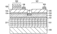
- FIG. 6A is a cross-sectional view schematically showing a first configuration example of the light emitting element according to the present embodiment.
- the light emitting element of the present embodiment has a first region 501 and a second region 502 in a plan view from a direction perpendicular to the substrate 100.
- the first region 501 mainly emits light of the first wavelength to the outside.
- the second region 502 mainly emits light having a second wavelength to the outside.
- the first region 501 and the second region 502 are formed on the same wafer.
- a first reflector 106 is arranged on the third semiconductor layer 105 of the second region 502. The first reflector 106 is not arranged on the third semiconductor layer 105 of the first region 501.
- the structure of the second region 502 is the same as the structure of FIG. 1 of the first embodiment. That is, the second region 502 is provided with a first reflector 106 having a high reflectance of light having a first wavelength.
- the first active layer 104 emits light having a first wavelength.
- the second active layer 102 is excited by the light of the first wavelength, and the second active layer 102 emits the light of the second wavelength.
- the first reflecting mirror 106 has a high reflectance with respect to light having a first wavelength. Therefore, light having a second wavelength is mainly emitted from the second region 502.
- a third electrode 503 is arranged on the third semiconductor layer 105 as an electrode for injecting a current into the first active layer 104 in the first region 501. ing.
- a current is injected into the first active layer 104 by the first electrode 107 and the third electrode 503, the first active layer 104 in the first region 501 emits light having a first wavelength.
- the first electrode 107 is a common electrode that supplies an electric current to the first active layer 104 in the first region 501 and the first active layer 104 in the second region 502.
- the second electrode 108 and the third electrode 503 are arranged independently of each other.
- the light emitting device of the present embodiment has a structure in which a current can be independently supplied to the first active layer 104 in the first region 501 and the first active layer 104 in the second region 502. Therefore, the first region 501 and the second region 502 can independently emit light having different wavelengths.
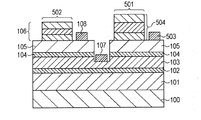
- FIG. 6B is a cross-sectional view schematically showing a second configuration example of the light emitting element according to the present embodiment.
- the first semiconductor layer 101 includes the second reflector 201, as in the second embodiment.
- the second reflector 201 is designed to have high reflectance for light of at least the first wavelength.
- the luminous efficiency of the light of the second wavelength is improved in the second region 502 for the same reason as in the second embodiment.
- the light of the first wavelength emitted downward from the first active layer 104 is reflected by the second reflecting mirror 201 and returned upward.
- the luminous efficiency of the light having the first wavelength is improved also in the first region 501.
- the luminous efficiency can be further improved.
- the second reflector 201 may be designed to have a high reflectance with respect to light having a second wavelength.
- the light of the second wavelength emitted downward from the second active layer 102 is also reflected by the second reflector 201 and returned upward.
- the luminous efficiency of the light of the second wavelength in the second region 502 is further improved.
- FIG. 6C is a cross-sectional view schematically showing a third configuration example of the light emitting element according to the present embodiment.
- This configuration example is one of the configurations for reducing the component of the second wavelength contained in the light emitted from the first region 501.
- a third reflector 504 is arranged on the third semiconductor layer 105 in the first region 501.
- the reflectance of the third reflector 504 to light of the second wavelength is higher than the reflectance to light of the first wavelength.
- Other configurations are the same as those of the first configuration example.
- the first active layer 104 emits light having a first wavelength.
- the second active layer 102 emits the light of the second wavelength. Since the light of the second wavelength is reflected by the third reflecting mirror 504, the component of the second wavelength contained in the light emitted from the first region 501 is reduced. Therefore, the proportion of the first wavelength contained in the light emitted from the first region 501 increases and the proportion of the second wavelength decreases, so that the light of the first wavelength and the light of the second wavelength Color mixing is reduced.
- the first region 501 and the second region 502 that emit light having different wavelengths can be formed on the same wafer. it can.
- the structure for changing the wavelength of the emitted light is the first reflector 106 arranged on the third semiconductor layer 105. Therefore, by forming the first reflecting mirror 106 at a desired location on the wafer surface, the first region 501 that emits light having different wavelengths from each other without processing the semiconductor layer under the first reflecting mirror 106. And the second region 502 can be formed. Therefore, it is possible to form a light emitting element capable of emitting light of two wavelengths individually by a simple process.
- the light emitting element of the present embodiment is obtained by modifying the number of light emitting regions of the third embodiment from two to three. That is, the light emitting element of the present embodiment is configured to be capable of emitting light of three different wavelengths from three light emitting regions formed on the same wafer.
- FIG. 7 is a cross-sectional view schematically showing a configuration example of the light emitting element according to the present embodiment.
- the light emitting device of the present embodiment has, in addition to the element structure of the second configuration example (FIG. 6B) of the third embodiment, a third region 601 that mainly emits light of a third wavelength to the outside. Further, in the present embodiment, a third reflector 504 is arranged on the third semiconductor layer 105 of the first region 501 as in the third configuration example (FIG. 6C) of the third embodiment. There is.
- the cross-sectional structure below the third semiconductor layer 105 is the same as in the first region 501 and the second region 502.
- a fourth semiconductor layer 604, a third active layer 602, and a fifth semiconductor layer 605 are arranged in this order on the third semiconductor layer 105.
- a fourth electrode 603 is arranged on the third semiconductor layer 105 as an electrode for injecting a current into the first active layer 104 in the third region 601. ing.
- the first active layer 104 in the third region 601 emits light having a first wavelength.
- the light of the first wavelength excites the third active layer 602, and the third active layer 602 emits the light of the third wavelength.
- the light of the third wavelength can be, for example, red light having a wavelength of about 630 nm.
- the first region 501, the second region 502, and the third region 601 that emit light having different wavelengths can be formed on the same wafer.
- the structure for changing the wavelength of the emitted light is such that each layer arranged on the third semiconductor layer 105, that is, the first reflecting mirror 106, the third reflecting mirror 504, and the fourth The semiconductor layer 604, the third active layer 602, and the fifth semiconductor layer 605. Therefore, by forming each of these layers at a desired location on the wafer surface, the first regions 501 and the second regions 501 and the second regions that emit light having different wavelengths from each other without processing the semiconductor layer under the layer. Region 502 and a third region 601 can be formed.
- light having a third wavelength is emitted by photoexcitation by light emission from the first active layer 104 in the third region 601.
- the fourth semiconductor layer 604, the third active layer 602, and the fifth semiconductor layer 605 do not need to be electrically connected to the third semiconductor layer 105, and are located at predetermined positions. It should be in. Therefore, it is possible to form a light emitting element capable of individually emitting light of three wavelengths in a simple process.
- the fourth semiconductor layer 604, the third active layer 602, and the fifth semiconductor layer 605 can be formed on the third semiconductor layer 105 by, for example, epitaxial growth. However, it may be formed by other methods.
- Another transfer substrate in which the fifth semiconductor layer 605, the third active layer 602, and the fourth semiconductor layer 604 are formed in this order from the substrate side is prepared in advance.
- This transfer substrate is bonded to the substrate 100 on which the semiconductor layer below the third semiconductor layer 105 is formed, and then only this transfer substrate is removed by wet etching or the like.
- the fourth semiconductor layer 604, the third active layer 602, and the fifth semiconductor layer 605 can be formed on the third semiconductor layer 105.
- Doping with a p-type dopant as described above may reduce the crystal quality of the semiconductor layer. Therefore, the crystal quality of a layer formed by epitaxial growth on a semiconductor layer doped with a p-type dopant may also deteriorate.
- the quality of the third active layer 602 can be improved and the light emission characteristics can be improved.
- the steps of determining the first region 501 and the second region 502, such as the formation of the first reflecting mirror 106 and the third reflecting mirror 504, include the fourth semiconductor layer 604, the third active layer 602, and the fifth. It is desirable that this is performed after joining the semiconductor layers 605 of the above and determining the position of the third region 601.
- the substrate can be bonded to a flat substrate immediately after epitaxial growth, instead of the uneven substrate that has undergone the process. As a result, the condition of the joint surface is improved, the process difficulty is lowered, and the yield is improved.
- the positions of the first region 501 and the second region 502 can be determined by the high position accuracy by photolithography with reference to the position of the third region 601 that has already been formed.
- the required accuracy in alignment at the time of joining can be lowered as compared with the case where the step of determining the first region 501 and the second region 502 is performed first. Further, as described above, as compared with the method of mounting the light emitting elements manufactured for each color on the substrate of the display, the elements of a plurality of colors can be arranged on the entire surface of the wafer by one bonding. Therefore, the effects of improving the yield and reducing the mounting cost can be obtained.
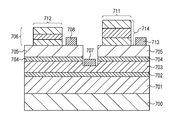
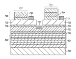
- FIG. 8 is a cross-sectional view schematically showing the structure of the light emitting element according to the present embodiment. Since the structure of the light emitting device of the present embodiment is the same as that of the third configuration example (FIG. 6C) of the third embodiment, detailed description of the structure may be omitted or simplified.
- the light emitting device of this embodiment is formed on a sapphire substrate 700 having an i-type GaN layer 701, an i-type green quantum well active layer 702, an n-type GaN layer 703, an i-type blue quantum well active layer 704, and a p-type. It is formed by sequentially epitaxially growing the GaN layer 705. A buffer layer (not shown) is formed between the sapphire substrate 700 and the GaN layer 701.
- the green quantum well active layer 702 includes an InGaN well layer and a GaN barrier layer.
- the In composition of the InGaN well layer is about 20%, and in this case, the central emission wavelength is 525 nm.
- the blue quantum well active layer 704 also includes an InGaN well layer and a GaN barrier layer.
- the In composition of the InGaN well layer is about 15%, and in this case, the central emission wavelength is 450 nm.
- the light emitting element of the present embodiment has a region 711 that emits blue light and a region 712 that emits green light in a plan view from a direction perpendicular to the sapphire substrate 700.
- the light emitting device is formed with a separation groove for separating the region 711 and the region 712. The depth of the separation groove is set so that the position of the bottom surface of the separation groove is between the upper surface and the lower surface of the GaN layer 703.
- an n-electrode 707 that gives a potential to each region in common is formed at the bottom of the separation groove.
- p electrodes 708 and 713 that individually apply potentials to the regions 712 and 711 are formed on the GaN layer 705.
- a reflector 706 that mainly reflects light having a blue wavelength and a reflector 714 that mainly reflects light having a green wavelength are formed in regions 712 and 711, respectively.
- the reflector 706 includes 6 pairs of laminated films of SiN and SiO 2 .
- the film thickness of each layer is determined in consideration of the refractive index of each layer so that the optical film thickness is 1/4 of the wavelength of blue light (450 nm).
- the reflector 714 contains 6 pairs of laminated films of SiN and SiO 2 . Each film thickness is determined in consideration of the refractive index of each film so that the optical film thickness is 1/4 of the wavelength of green light (525 nm).
- a light emitting element in which a region 711 that emits light having a blue wavelength and a region 712 that emits light having a green wavelength are formed on the same wafer can be manufactured by a simple process.
- FIG. 9 is a cross-sectional view schematically showing the structure of the light emitting element according to the present embodiment.
- the i-type GaN layer 801 includes the i-type DBR layer 802. Since the structures other than this are the same as those in the fifth embodiment, the description thereof will be omitted.
- the DBR layer 802 has a laminated structure in which a plurality of pairs of AlGaN layers and GaN layers are alternately laminated.
- the film thickness of each layer is determined in consideration of the refractive index of each layer so that the optical film thickness is 1/4 of the wavelength of blue light (450 nm). Further, the film thickness and the like of each layer are set so that the DBR layer 802 and the reflector 706 form a resonator for the blue wavelength.
- blue (wavelength 450 nm) light resonates in the resonator in the region 712.
- the absorption rate of blue light in the green quantum well active layer 702 increases, and the luminous efficiency of green light from the green quantum well active layer 702 is improved.
- the light emitted to the sapphire substrate 700 side is reflected by the DBR layer 802 and heads upward, so that the luminous efficiency of the blue light is improved. To do.
- the luminous efficiency of blue and green light is further improved as compared with the fifth embodiment.
- FIG. 10 is a cross-sectional view schematically showing the structure of the light emitting element according to the present embodiment.
- the light emitting element of the present embodiment further has a region 901 that emits red light in a plan view from a direction perpendicular to the sapphire substrate 700. Since the structure other than this is the same as that of the sixth embodiment, the description thereof will be omitted.
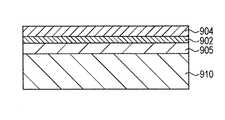
- the AlInP clad layer 904, the AlGaInP active layer 902, and the AlInP clad layer 905 are formed on the GaN layer 705 in this order.
- the ratio of each element of the AlGaInP active layer 902 is adjusted so that the central emission wavelength thereof is 630 nm.
- a p-electrode 903 that gives a potential to the region 901 is formed.
- the blue quantum well active layer 704 emits blue light.
- the AlGaInP active layer 902 is excited by the blue light, and the AlGaInP active layer 902 emits red light. As a result, red light is emitted from the region 901.
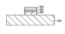
- FIGS. 11A and 11B are cross-sectional views schematically showing the structure of the transfer substrate according to the present embodiment.
- the AlInP clad layer 905, the AlGaInP active layer 902, and the AlInP clad layer 904 are formed by epitaxially growing on a GaAs substrate 910 different from the sapphire substrate 700 in this order.
- patterning is performed by etching the AlInP clad layer 904, the AlGaInP active layer 902, and the AlInP clad layer 905 so as to leave only the portion corresponding to the light emitting region.
- a polyimide layer (not shown) is formed on the upper surface of FIG. 11B by spin coating.
- the GaN layer 705 of the sapphire substrate 700 on which the layers up to the GaN layer 705 shown in FIG. 10 are formed and the AlInP clad layer 904 of the transfer substrate are heated in a aligned state so as to face each other.
- the GaN layer 705 and the AlInP clad layer 904 are joined via the polyimide layer.
- the GaAs substrate 910 is removed by wet etching.
- the AlInP clad layer 904, the AlGaInP active layer 902, and the AlInP clad layer 905 are transferred onto the GaN layer 705.
- the separation groove 906 is formed, the reflectors 706 and 714 are formed, and the like as in the fifth embodiment, and the light emitting element shown in FIG. 10 is completed.
- the region 711 that emits light having a blue wavelength, the region 712 that emits light having a green wavelength, and the region 901 that emits light having a red wavelength are formed on the same wafer.
- the light emitting element can be manufactured by a simple process.
Landscapes
- Led Devices (AREA)
Priority Applications (4)
| Application Number | Priority Date | Filing Date | Title |
|---|---|---|---|
| EP20846408.1A EP4006995A4 (en) | 2019-07-30 | 2020-07-28 | Light-emitting element, and method for manufacturing light-emitting element |
| CN202080054210.2A CN114175281B (zh) | 2019-07-30 | 2020-07-28 | 发光元件和发光元件的制造方法 |
| KR1020227000428A KR102647549B1 (ko) | 2019-07-30 | 2020-07-28 | 발광 소자 및 발광 소자의 제조방법 |
| US17/577,598 US12002840B2 (en) | 2019-07-30 | 2022-01-18 | Light emitting element and manufacturing method of light emitting element |
Applications Claiming Priority (2)
| Application Number | Priority Date | Filing Date | Title |
|---|---|---|---|
| JP2019-139551 | 2019-07-30 | ||
| JP2019139551A JP7414419B2 (ja) | 2019-07-30 | 2019-07-30 | 発光素子及び発光素子の製造方法 |
Related Child Applications (1)
| Application Number | Title | Priority Date | Filing Date |
|---|---|---|---|
| US17/577,598 Continuation US12002840B2 (en) | 2019-07-30 | 2022-01-18 | Light emitting element and manufacturing method of light emitting element |
Publications (1)
| Publication Number | Publication Date |
|---|---|
| WO2021020378A1 true WO2021020378A1 (ja) | 2021-02-04 |
Family
ID=74229091
Family Applications (1)
| Application Number | Title | Priority Date | Filing Date |
|---|---|---|---|
| PCT/JP2020/028840 Ceased WO2021020378A1 (ja) | 2019-07-30 | 2020-07-28 | 発光素子及び発光素子の製造方法 |
Country Status (6)
| Country | Link |
|---|---|
| US (1) | US12002840B2 (enExample) |
| EP (1) | EP4006995A4 (enExample) |
| JP (1) | JP7414419B2 (enExample) |
| KR (1) | KR102647549B1 (enExample) |
| CN (1) | CN114175281B (enExample) |
| WO (1) | WO2021020378A1 (enExample) |
Cited By (1)
| Publication number | Priority date | Publication date | Assignee | Title |
|---|---|---|---|---|
| US12002840B2 (en) | 2019-07-30 | 2024-06-04 | Canon Kabushiki Kaisha | Light emitting element and manufacturing method of light emitting element |
Families Citing this family (7)
| Publication number | Priority date | Publication date | Assignee | Title |
|---|---|---|---|---|
| JP7472820B2 (ja) | 2021-02-16 | 2024-04-23 | 株式会社Soken | 物体検知装置 |
| US12300770B2 (en) | 2021-03-03 | 2025-05-13 | Toyoda Gosei Co., Ltd. | Flip-chip mounted monolithic micro LED display element including a plurality of light-emitting parts arranged in a matrix |
| JP7563254B2 (ja) * | 2021-03-11 | 2024-10-08 | 豊田合成株式会社 | 発光素子とその製造方法 |
| KR20230120921A (ko) | 2022-02-10 | 2023-08-17 | 삼성전자주식회사 | 반도체 발광 소자, 및 그 발광 소자를 포함한 발광 소자 어셈블리 |
| US12278256B2 (en) | 2022-12-15 | 2025-04-15 | Samsung Electronics Co., Ltd. | Display apparatus including LED with plurality of light emitting layers |
| WO2024170075A1 (en) * | 2023-02-15 | 2024-08-22 | Crocus Labs GmbH | Monolithic multi-color led device |
| CN119521910A (zh) * | 2023-08-15 | 2025-02-25 | 武汉华星光电半导体显示技术有限公司 | 显示面板及显示装置 |
Citations (7)
| Publication number | Priority date | Publication date | Assignee | Title |
|---|---|---|---|---|
| JPH11274558A (ja) * | 1998-03-23 | 1999-10-08 | Toshiba Corp | 半導体発光素子および半導体発光装置 |
| JP2009070893A (ja) | 2007-09-11 | 2009-04-02 | Rohm Co Ltd | 発光装置及びその製造方法 |
| JP2009212308A (ja) * | 2008-03-04 | 2009-09-17 | Sumitomo Electric Ind Ltd | 発光ダイオード |
| JP2010541217A (ja) * | 2007-09-28 | 2010-12-24 | オスラム オプト セミコンダクターズ ゲゼルシャフト ミット ベシュレンクテル ハフツング | 放射放出用の半導体ボディ |
| JP2012521644A (ja) * | 2009-03-25 | 2012-09-13 | オスラム オプト セミコンダクターズ ゲゼルシャフト ミット ベシュレンクテル ハフツング | 発光ダイオード |
| US20190158352A1 (en) * | 2014-11-21 | 2019-05-23 | Epistar Corporation | Light-emitting device |
| JP2019139551A (ja) | 2018-02-13 | 2019-08-22 | 沖電気工業株式会社 | 文字認識装置 |
Family Cites Families (19)
| Publication number | Priority date | Publication date | Assignee | Title |
|---|---|---|---|---|
| JPH06310804A (ja) * | 1993-04-20 | 1994-11-04 | Sanyo Electric Co Ltd | 面発光レーザ素子 |
| JPH08288549A (ja) | 1995-04-11 | 1996-11-01 | Omron Corp | 多波長発光半導体素子 |
| US5898722A (en) * | 1997-03-10 | 1999-04-27 | Motorola, Inc. | Dual wavelength monolithically integrated vertical cavity surface emitting lasers and method of fabrication |
| US8829546B2 (en) | 1999-11-19 | 2014-09-09 | Cree, Inc. | Rare earth doped layer or substrate for light conversion |
| JP3667188B2 (ja) * | 2000-03-03 | 2005-07-06 | キヤノン株式会社 | 電子線励起レーザー装置及びマルチ電子線励起レーザー装置 |
| JP2002289965A (ja) * | 2001-03-23 | 2002-10-04 | Matsushita Electric Ind Co Ltd | 半導体レーザ装置、及び光ピックアップ装置 |
| JP4307113B2 (ja) | 2002-03-19 | 2009-08-05 | 宣彦 澤木 | 半導体発光素子およびその製造方法 |
| US7402831B2 (en) * | 2004-12-09 | 2008-07-22 | 3M Innovative Properties Company | Adapting short-wavelength LED's for polychromatic, broadband, or “white” emission |
| JP2006351966A (ja) | 2005-06-17 | 2006-12-28 | Sony Corp | 多波長半導体レーザ素子 |
| JP4874768B2 (ja) | 2006-11-14 | 2012-02-15 | 株式会社リコー | 波長変換素子 |
| WO2009048425A1 (en) | 2007-10-12 | 2009-04-16 | Agency For Science, Technology And Research | Fabrication of phosphor free red and white nitride-based leds |
| US7839913B2 (en) * | 2007-11-22 | 2010-11-23 | Canon Kabushiki Kaisha | Surface emitting laser, surface emitting laser array, and image forming apparatus including surface emitting laser |
| JP5590829B2 (ja) * | 2009-07-03 | 2014-09-17 | キヤノン株式会社 | 面発光レーザ、面発光レーザアレイ及び画像形成装置 |
| JP5871458B2 (ja) * | 2010-11-02 | 2016-03-01 | キヤノン株式会社 | 垂直共振器型面発光レーザ、画像形成装置 |
| JP6136284B2 (ja) | 2012-03-13 | 2017-05-31 | 株式会社リコー | 半導体積層体及び面発光レーザ素子 |
| FR3019380B1 (fr) | 2014-04-01 | 2017-09-01 | Centre Nat Rech Scient | Pixel semiconducteur, matrice de tels pixels, structure semiconductrice pour la realisation de tels pixels et leurs procedes de fabrication |
| DE102018111021A1 (de) | 2017-12-14 | 2019-06-19 | Osram Opto Semiconductors Gmbh | Lichtemittierendes halbleiterbauteil und verfahren zur herstellung eines licht emittierenden halbleiterbauteils |
| JP7248441B2 (ja) | 2018-03-02 | 2023-03-29 | シャープ株式会社 | 画像表示素子 |
| JP7414419B2 (ja) | 2019-07-30 | 2024-01-16 | キヤノン株式会社 | 発光素子及び発光素子の製造方法 |
-
2019
- 2019-07-30 JP JP2019139551A patent/JP7414419B2/ja active Active
-
2020
- 2020-07-28 WO PCT/JP2020/028840 patent/WO2021020378A1/ja not_active Ceased
- 2020-07-28 EP EP20846408.1A patent/EP4006995A4/en active Pending
- 2020-07-28 CN CN202080054210.2A patent/CN114175281B/zh active Active
- 2020-07-28 KR KR1020227000428A patent/KR102647549B1/ko active Active
-
2022
- 2022-01-18 US US17/577,598 patent/US12002840B2/en active Active
Patent Citations (7)
| Publication number | Priority date | Publication date | Assignee | Title |
|---|---|---|---|---|
| JPH11274558A (ja) * | 1998-03-23 | 1999-10-08 | Toshiba Corp | 半導体発光素子および半導体発光装置 |
| JP2009070893A (ja) | 2007-09-11 | 2009-04-02 | Rohm Co Ltd | 発光装置及びその製造方法 |
| JP2010541217A (ja) * | 2007-09-28 | 2010-12-24 | オスラム オプト セミコンダクターズ ゲゼルシャフト ミット ベシュレンクテル ハフツング | 放射放出用の半導体ボディ |
| JP2009212308A (ja) * | 2008-03-04 | 2009-09-17 | Sumitomo Electric Ind Ltd | 発光ダイオード |
| JP2012521644A (ja) * | 2009-03-25 | 2012-09-13 | オスラム オプト セミコンダクターズ ゲゼルシャフト ミット ベシュレンクテル ハフツング | 発光ダイオード |
| US20190158352A1 (en) * | 2014-11-21 | 2019-05-23 | Epistar Corporation | Light-emitting device |
| JP2019139551A (ja) | 2018-02-13 | 2019-08-22 | 沖電気工業株式会社 | 文字認識装置 |
Non-Patent Citations (1)
| Title |
|---|
| See also references of EP4006995A4 |
Cited By (1)
| Publication number | Priority date | Publication date | Assignee | Title |
|---|---|---|---|---|
| US12002840B2 (en) | 2019-07-30 | 2024-06-04 | Canon Kabushiki Kaisha | Light emitting element and manufacturing method of light emitting element |
Also Published As
| Publication number | Publication date |
|---|---|
| KR102647549B1 (ko) | 2024-03-14 |
| EP4006995A4 (en) | 2023-08-30 |
| US20220139997A1 (en) | 2022-05-05 |
| US12002840B2 (en) | 2024-06-04 |
| JP7414419B2 (ja) | 2024-01-16 |
| KR20220018017A (ko) | 2022-02-14 |
| CN114175281B (zh) | 2024-12-31 |
| JP2021022688A (ja) | 2021-02-18 |
| CN114175281A (zh) | 2022-03-11 |
| EP4006995A1 (en) | 2022-06-01 |
Similar Documents
| Publication | Publication Date | Title |
|---|---|---|
| US12002840B2 (en) | Light emitting element and manufacturing method of light emitting element | |
| JP2002222989A (ja) | 半導体発光素子 | |
| KR100689782B1 (ko) | 반도체 발광 소자 및 그 제조 방법 | |
| JP2011510497A (ja) | 光量子リングレーザ及びその製造方法 | |
| CN105633229B (zh) | 发光二极管及其制作方法 | |
| CN114389149B (zh) | 发光装置及投影仪 | |
| WO2018020793A1 (ja) | 半導体発光素子および半導体発光素子の製造方法 | |
| US11177316B2 (en) | Method of manufacturing light emitting device, light emitting device, and projector | |
| JP6159642B2 (ja) | 発光素子 | |
| KR20050034970A (ko) | 수직 공진기형 발광소자 및 제조방법 | |
| KR20250134676A (ko) | 마이크로-발광 다이오드들을 위한 컬러 필터링 분산 브래그 반사기 및 그 제작 방법 | |
| KR101165258B1 (ko) | 발광 소자 및 이의 제조 방법 | |
| JP2002305327A (ja) | 窒化物系半導体発光素子 | |
| WO2023007837A1 (ja) | 窒化物半導体発光素子 | |
| JP7485278B2 (ja) | 発光装置およびプロジェクター | |
| WO2022109781A1 (zh) | 量子阱结构及其制备方法和发光二极管 | |
| US20240243226A1 (en) | Resonant cavity micro-led fabrication | |
| US20240243232A1 (en) | Micro-led dbr fabrication by electrochemical etching | |
| US20240243225A1 (en) | Color filtering dbr for micro-leds | |
| JP7616598B2 (ja) | フォトニック結晶構造体の製造方法、フォトニック結晶構造体、発光装置、およびプロジェクター | |
| KR20250134675A (ko) | 전기화학적 에칭에 의한 마이크로-led dbr 제작 | |
| EP4652634A1 (en) | Resonant cavity micro-led fabrication | |
| CN120240012A (zh) | 用于制造光电子半导体器件的方法和光电子半导体器件 | |
| JP5153524B2 (ja) | 窒化物半導体発光素子およびその製造方法 |
Legal Events
| Date | Code | Title | Description |
|---|---|---|---|
| 121 | Ep: the epo has been informed by wipo that ep was designated in this application |
Ref document number: 20846408 Country of ref document: EP Kind code of ref document: A1 |
|
| ENP | Entry into the national phase |
Ref document number: 20227000428 Country of ref document: KR Kind code of ref document: A |
|
| NENP | Non-entry into the national phase |
Ref country code: DE |
|
| ENP | Entry into the national phase |
Ref document number: 2020846408 Country of ref document: EP Effective date: 20220228 |
|
| WWG | Wipo information: grant in national office |
Ref document number: 202080054210.2 Country of ref document: CN |