WO2021014258A1 - 撮像装置および電子機器 - Google Patents
撮像装置および電子機器 Download PDFInfo
- Publication number
- WO2021014258A1 WO2021014258A1 PCT/IB2020/056448 IB2020056448W WO2021014258A1 WO 2021014258 A1 WO2021014258 A1 WO 2021014258A1 IB 2020056448 W IB2020056448 W IB 2020056448W WO 2021014258 A1 WO2021014258 A1 WO 2021014258A1
- Authority
- WO
- WIPO (PCT)
- Prior art keywords
- transistor
- layer
- data
- wiring
- circuit
- Prior art date
- Legal status (The legal status is an assumption and is not a legal conclusion. Google has not performed a legal analysis and makes no representation as to the accuracy of the status listed.)
- Ceased
Links
Images




















Classifications
-
- H—ELECTRICITY
- H04—ELECTRIC COMMUNICATION TECHNIQUE
- H04N—PICTORIAL COMMUNICATION, e.g. TELEVISION
- H04N23/00—Cameras or camera modules comprising electronic image sensors; Control thereof
- H04N23/60—Control of cameras or camera modules
- H04N23/63—Control of cameras or camera modules by using electronic viewfinders
- H04N23/631—Graphical user interfaces [GUI] specially adapted for controlling image capture or setting capture parameters
-
- H—ELECTRICITY
- H10—SEMICONDUCTOR DEVICES; ELECTRIC SOLID-STATE DEVICES NOT OTHERWISE PROVIDED FOR
- H10F—INORGANIC SEMICONDUCTOR DEVICES SENSITIVE TO INFRARED RADIATION, LIGHT, ELECTROMAGNETIC RADIATION OF SHORTER WAVELENGTH OR CORPUSCULAR RADIATION
- H10F39/00—Integrated devices, or assemblies of multiple devices, comprising at least one element covered by group H10F30/00, e.g. radiation detectors comprising photodiode arrays
- H10F39/80—Constructional details of image sensors
- H10F39/803—Pixels having integrated switching, control, storage or amplification elements
-
- H—ELECTRICITY
- H04—ELECTRIC COMMUNICATION TECHNIQUE
- H04N—PICTORIAL COMMUNICATION, e.g. TELEVISION
- H04N25/00—Circuitry of solid-state image sensors [SSIS]; Control thereof
- H04N25/40—Extracting pixel data from image sensors by controlling scanning circuits, e.g. by modifying the number of pixels sampled or to be sampled
- H04N25/46—Extracting pixel data from image sensors by controlling scanning circuits, e.g. by modifying the number of pixels sampled or to be sampled by combining or binning pixels
-
- H—ELECTRICITY
- H04—ELECTRIC COMMUNICATION TECHNIQUE
- H04N—PICTORIAL COMMUNICATION, e.g. TELEVISION
- H04N25/00—Circuitry of solid-state image sensors [SSIS]; Control thereof
- H04N25/70—SSIS architectures; Circuits associated therewith
- H04N25/71—Charge-coupled device [CCD] sensors; Charge-transfer registers specially adapted for CCD sensors
- H04N25/745—Circuitry for generating timing or clock signals
-
- H—ELECTRICITY
- H04—ELECTRIC COMMUNICATION TECHNIQUE
- H04N—PICTORIAL COMMUNICATION, e.g. TELEVISION
- H04N25/00—Circuitry of solid-state image sensors [SSIS]; Control thereof
- H04N25/70—SSIS architectures; Circuits associated therewith
- H04N25/71—Charge-coupled device [CCD] sensors; Charge-transfer registers specially adapted for CCD sensors
- H04N25/75—Circuitry for providing, modifying or processing image signals from the pixel array
-
- H—ELECTRICITY
- H04—ELECTRIC COMMUNICATION TECHNIQUE
- H04N—PICTORIAL COMMUNICATION, e.g. TELEVISION
- H04N25/00—Circuitry of solid-state image sensors [SSIS]; Control thereof
- H04N25/70—SSIS architectures; Circuits associated therewith
- H04N25/76—Addressed sensors, e.g. MOS or CMOS sensors
- H04N25/77—Pixel circuitry, e.g. memories, A/D converters, pixel amplifiers, shared circuits or shared components
-
- H—ELECTRICITY
- H04—ELECTRIC COMMUNICATION TECHNIQUE
- H04N—PICTORIAL COMMUNICATION, e.g. TELEVISION
- H04N25/00—Circuitry of solid-state image sensors [SSIS]; Control thereof
- H04N25/70—SSIS architectures; Circuits associated therewith
- H04N25/76—Addressed sensors, e.g. MOS or CMOS sensors
- H04N25/7795—Circuitry for generating timing or clock signals
-
- H—ELECTRICITY
- H10—SEMICONDUCTOR DEVICES; ELECTRIC SOLID-STATE DEVICES NOT OTHERWISE PROVIDED FOR
- H10F—INORGANIC SEMICONDUCTOR DEVICES SENSITIVE TO INFRARED RADIATION, LIGHT, ELECTROMAGNETIC RADIATION OF SHORTER WAVELENGTH OR CORPUSCULAR RADIATION
- H10F39/00—Integrated devices, or assemblies of multiple devices, comprising at least one element covered by group H10F30/00, e.g. radiation detectors comprising photodiode arrays
- H10F39/10—Integrated devices
- H10F39/12—Image sensors
-
- H—ELECTRICITY
- H10—SEMICONDUCTOR DEVICES; ELECTRIC SOLID-STATE DEVICES NOT OTHERWISE PROVIDED FOR
- H10F—INORGANIC SEMICONDUCTOR DEVICES SENSITIVE TO INFRARED RADIATION, LIGHT, ELECTROMAGNETIC RADIATION OF SHORTER WAVELENGTH OR CORPUSCULAR RADIATION
- H10F39/00—Integrated devices, or assemblies of multiple devices, comprising at least one element covered by group H10F30/00, e.g. radiation detectors comprising photodiode arrays
- H10F39/10—Integrated devices
- H10F39/12—Image sensors
- H10F39/18—Complementary metal-oxide-semiconductor [CMOS] image sensors; Photodiode array image sensors
-
- H—ELECTRICITY
- H10—SEMICONDUCTOR DEVICES; ELECTRIC SOLID-STATE DEVICES NOT OTHERWISE PROVIDED FOR
- H10F—INORGANIC SEMICONDUCTOR DEVICES SENSITIVE TO INFRARED RADIATION, LIGHT, ELECTROMAGNETIC RADIATION OF SHORTER WAVELENGTH OR CORPUSCULAR RADIATION
- H10F39/00—Integrated devices, or assemblies of multiple devices, comprising at least one element covered by group H10F30/00, e.g. radiation detectors comprising photodiode arrays
- H10F39/80—Constructional details of image sensors
- H10F39/802—Geometry or disposition of elements in pixels, e.g. address-lines or gate electrodes
- H10F39/8023—Disposition of the elements in pixels, e.g. smaller elements in the centre of the imager compared to larger elements at the periphery
-
- H—ELECTRICITY
- H10—SEMICONDUCTOR DEVICES; ELECTRIC SOLID-STATE DEVICES NOT OTHERWISE PROVIDED FOR
- H10F—INORGANIC SEMICONDUCTOR DEVICES SENSITIVE TO INFRARED RADIATION, LIGHT, ELECTROMAGNETIC RADIATION OF SHORTER WAVELENGTH OR CORPUSCULAR RADIATION
- H10F39/00—Integrated devices, or assemblies of multiple devices, comprising at least one element covered by group H10F30/00, e.g. radiation detectors comprising photodiode arrays
- H10F39/80—Constructional details of image sensors
- H10F39/802—Geometry or disposition of elements in pixels, e.g. address-lines or gate electrodes
- H10F39/8027—Geometry of the photosensitive area
-
- H—ELECTRICITY
- H10—SEMICONDUCTOR DEVICES; ELECTRIC SOLID-STATE DEVICES NOT OTHERWISE PROVIDED FOR
- H10F—INORGANIC SEMICONDUCTOR DEVICES SENSITIVE TO INFRARED RADIATION, LIGHT, ELECTROMAGNETIC RADIATION OF SHORTER WAVELENGTH OR CORPUSCULAR RADIATION
- H10F39/00—Integrated devices, or assemblies of multiple devices, comprising at least one element covered by group H10F30/00, e.g. radiation detectors comprising photodiode arrays
- H10F39/80—Constructional details of image sensors
- H10F39/803—Pixels having integrated switching, control, storage or amplification elements
- H10F39/8037—Pixels having integrated switching, control, storage or amplification elements the integrated elements comprising a transistor
-
- H—ELECTRICITY
- H10—SEMICONDUCTOR DEVICES; ELECTRIC SOLID-STATE DEVICES NOT OTHERWISE PROVIDED FOR
- H10F—INORGANIC SEMICONDUCTOR DEVICES SENSITIVE TO INFRARED RADIATION, LIGHT, ELECTROMAGNETIC RADIATION OF SHORTER WAVELENGTH OR CORPUSCULAR RADIATION
- H10F39/00—Integrated devices, or assemblies of multiple devices, comprising at least one element covered by group H10F30/00, e.g. radiation detectors comprising photodiode arrays
- H10F39/80—Constructional details of image sensors
- H10F39/803—Pixels having integrated switching, control, storage or amplification elements
- H10F39/8037—Pixels having integrated switching, control, storage or amplification elements the integrated elements comprising a transistor
- H10F39/80377—Pixels having integrated switching, control, storage or amplification elements the integrated elements comprising a transistor characterised by the channel of the transistor, e.g. channel having a doping gradient
Definitions
- One aspect of the present invention relates to an imaging device.
- one aspect of the present invention is not limited to the above technical fields.
- the technical field of one aspect of the invention disclosed in the present specification and the like relates to a product, a method, or a manufacturing method.
- one aspect of the invention relates to a process, machine, manufacture, or composition (composition of matter). Therefore, more specifically, the technical fields of one aspect of the present invention disclosed in the present specification include semiconductor devices, display devices, liquid crystal display devices, light emitting devices, lighting devices, power storage devices, storage devices, imaging devices, and the like.
- the driving method or the manufacturing method thereof can be given as an example.
- the semiconductor device refers to all devices that can function by utilizing the semiconductor characteristics.
- Transistors and semiconductor circuits are one aspect of semiconductor devices.
- the storage device, the display device, the image pickup device, and the electronic device may have a semiconductor device.
- Patent Document 1 discloses an image pickup apparatus having an oxide semiconductor and using a transistor having an extremely low off-current in a pixel circuit.
- Patent Document 2 discloses a technique for adding an arithmetic function to an imaging device.
- Patent Document 3 shows an image sensor in which a plurality of sensor chips are bonded.
- Japanese Unexamined Patent Publication No. 2011-119711 Japanese Unexamined Patent Publication No. 2016-123087 Japanese Unexamined Patent Publication No. 2018-117027
- an image pickup device equipped with a solid-state image sensor such as a CMOS image sensor high-quality images can be easily taken due to technological development.
- the imaging device it is required that the imaging device be equipped with more intelligent functions.
- image data compression and image recognition are processed after the image data (analog data) is converted to digital data and taken out of the imaging device. If the processing can be performed in the imaging device, the cooperation with an external device becomes faster and the convenience of the user is improved. In addition, the load and power consumption of peripheral devices can be reduced. Further, if complicated data processing can be performed in the state of analog data, the time required for data conversion can be shortened.
- one aspect of the present invention is to provide an image pickup apparatus capable of performing image processing.
- one of the purposes is to provide an image pickup device with low power consumption.
- one of the purposes is to provide a highly reliable imaging device.
- one of the purposes is to provide a new imaging device or the like.
- Another object of the present invention is to provide a method for driving the image pickup apparatus.
- one aspect of the present invention is to provide an imaging device capable of performing data processing while suppressing fluctuations in analog data.
- Another object of the present invention is to provide an image pickup apparatus capable of processing analog data while suppressing power consumption.
- Another object of the present invention is to provide an imaging device having a reduced circuit area.
- Another object of the present invention is to provide an image pickup apparatus in which the area of the photoelectric conversion device is increased.
- Another object of the present invention is to provide an image pickup apparatus in which the degree of pixel integration is increased.
- one of the purposes is to provide a low-cost imaging device.
- one of the purposes is to provide a new semiconductor device or the like.
- One aspect of the present invention relates to an imaging device capable of arithmetically processing the data while holding the data in the pixels.
- One aspect of the present invention includes a pixel block and a first circuit, the pixel block has a plurality of pixels arranged in a matrix, and the pixel block and the first circuit are electrically connected.
- Each of the plurality of pixels has a photoelectric conversion device, a first transistor, a second transistor, and a capacitor, and the photoelectric conversion device and the first transistor are formed in the first layer.
- the capacitor is formed in a second layer, the second layer is joined to the first layer, the first transistor and the second transistor each have silicon in the channel forming region, and the first transistor.
- One of the source or drain of the second transistor is electrically connected to one electrode of the photoelectric conversion device, the other is electrically connected to one electrode of the capacitor, and one of the source or drain of the second transistor is the other of the capacitor. It is electrically connected to the electrode, and each of the plurality of pixels has a function of generating the first data and a function of multiplying the first data by an arbitrary magnification to generate the second data.
- the first circuit corresponds to the function of generating the third data corresponding to the sum of the first data generated by each of the plurality of pixels and the sum of the second data generated by each of the plurality of pixels.
- the plurality of pixels of the pixel block and the first circuit are electrically connected.
- one aspect of the present invention includes a pixel block and a first circuit
- the pixel block has a plurality of pixels arranged in a matrix, and the plurality of pixels and the first circuit are Electrically connected
- each of the plurality of pixels has a photoelectric conversion device, a first transistor, a second transistor, and a capacitor
- the photoelectric conversion device and the first transistor are the first layer.
- the capacitor and the second transistor are formed in the second layer, the second layer is bonded to the first layer by the bonding process, and the first transistor and the second transistor are respectively formed.
- silicon in the channel formation region one of the source or drain of the first transistor is electrically connected to one electrode of the photoelectric conversion device and the other is electrically connected to one electrode of the capacitor.
- the first circuit has a function of generating a second data
- the first circuit has a function of generating a third data corresponding to the sum of the first data generated by each of the plurality of pixels and a plurality of functions. It has a function of adding a potential corresponding to the sum of the second data generated by each of the pixels to the third data by capacitance coupling to generate the fourth data, and has the first data and the second data.
- the data of is an image pickup device which is an analog value.
- the first layer is formed on the first silicon substrate, and the n-type region of the photoelectric conversion device and one of the source and drain of the first transistor may be shared. preferable.
- the capacitor is preferably a trench capacitor.
- one aspect of the present invention is an electronic device having the image pickup device and the display device described above.
- an image pickup apparatus capable of performing image processing. Further, it is possible to provide an image pickup device having low power consumption. Further, it is possible to provide a highly reliable imaging device. In addition, a new imaging device or the like can be provided. Further, it is possible to provide a method for driving the image pickup apparatus.
- an imaging device capable of performing data processing while suppressing fluctuations in analog data. Further, it is possible to provide an image pickup apparatus capable of processing analog data while suppressing power consumption. Further, it is possible to provide an imaging device having a reduced circuit area. Further, it is possible to provide an image pickup apparatus in which the area of the photoelectric conversion device is increased. In addition, it is possible to provide an imaging device having an increased degree of pixel integration. Further, it is possible to provide an image pickup apparatus having a low cost. Further, it is possible to provide a new semiconductor device or the like.
- FIG. 1 is a block diagram illustrating an imaging device.
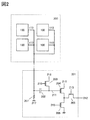
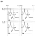
- FIG. 2 is a diagram illustrating the pixel block 200 and the circuit 201.
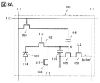
- 3A and 3B are diagrams for explaining the pixel 100.
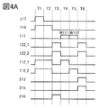
- 4A and 4B are timing charts illustrating the operation of the pixel block 200 and the circuit 201.
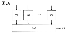
- 5A and 5B are diagrams for explaining the circuit 301 and the circuit 302.
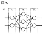
- FIG. 6 is a diagram illustrating pixels included in the circuit 302. 7A and 7B are diagrams showing a configuration example of a neural network.
- FIG. 8 is a diagram illustrating the circuit 304.
- FIG. 9 is a timing chart illustrating the operation of the circuit 304.
- FIG. 10 is a timing chart illustrating the operation of the circuit 304.
- FIG. 11A is a diagram illustrating the operation of the rolling shutter.
- FIG. 11B is a diagram illustrating the operation of the global shutter.
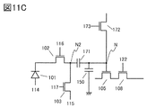
- FIG. 11C is an example of a pixel.
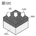
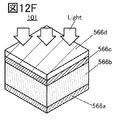
- 12A to 12F are diagrams for explaining the configuration of pixels of the image pickup apparatus.
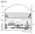
- FIG. 13A is a cross-sectional view illustrating the pixels.
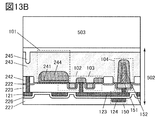
- FIG. 13B is a cross-sectional view illustrating the pixels.
- FIG. 14 is a cross-sectional view illustrating the pixels.
- FIG. 15 is a cross-sectional view illustrating the pixels.
- FIG. 16A is a cross-sectional view illustrating the pixels.
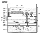
- FIG. 16B is a cross-sectional view illustrating the pixels.
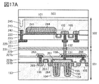
- FIG. 17A is a cross-sectional view illustrating the pixels.
- 17B is a cross-sectional view illustrating the pixels.
- 18A to 18C are diagrams for explaining Si transistors.
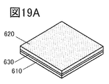
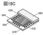
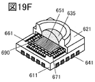
- 19A to 19F are perspective views of a package and a module containing an imaging device.
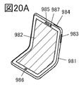
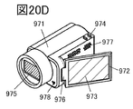
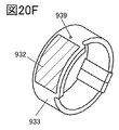
- 20A to 20F are diagrams for explaining an electronic device.
- the element may be composed of a plurality of elements as long as there is no functional inconvenience.
- a plurality of transistors operating as switches may be connected in series or in parallel.
- the capacitor may be divided and arranged at a plurality of positions.
- one conductor may have a plurality of functions such as wiring, electrodes and terminals, and in the present specification, a plurality of names may be used for the same element. Further, even when the elements are shown to be directly connected on the circuit diagram, the elements may actually be connected to each other via a plurality of conductors. In the book, such a configuration is also included in the category of direct connection.
- the imaging device holds analog data (image data) acquired in the imaging operation in pixels, and can extract data obtained by multiplying the analog data by an arbitrary weighting coefficient.
- processing such as image recognition can be performed. Since a huge amount of image data can be held in pixels in the state of analog data, processing can be performed efficiently.
- FIG. 1 is a block diagram illustrating an imaging device according to an aspect of the present invention.
- the imaging device includes a pixel array 300, a circuit 201, a circuit 301, a circuit 302, a circuit 303, a circuit 304, and a circuit 305.
- the circuit 201 and the circuits 301 to 305 are not limited to a single circuit configuration, and may be composed of a plurality of circuits. Alternatively, any one of the above circuits may be integrated.
- the pixel array 300 has an imaging function and a calculation function.
- the circuits 201 and 301 have an arithmetic function.
- the circuit 302 has an arithmetic function or a data conversion function.
- the circuits 303 and 304 have a selection function.
- the circuit 305 has a function of supplying an electric potential to the pixel.
- the pixel array 300 has a plurality of pixel blocks 200. As shown in FIG. 2, the pixel block 200 has a plurality of pixels 100 arranged in a matrix, and each pixel 100 is electrically connected to the circuit 201.
- the circuit 201 can also be provided in the pixel block 200.
- Image data can be acquired with pixel 100.
- the number of pixels is set to 2 ⁇ 2 as an example, but the number is not limited to this.
- the pixel block 200 operates as a product-sum calculation circuit. Further, the circuit 201 electrically connected to the pixel block 200 has a function of extracting the product of the image data and the weighting coefficient from the pixel 100. The circuit 201 also has a function as a correlated double sampling circuit (CDS circuit).
- CDS circuit correlated double sampling circuit
- the pixel 100 can include a photoelectric conversion device 101, a transistor 102, a transistor 103, a capacitor 104, a transistor 105, a transistor 106, a transistor 108, and a capacitor 150. ..
- One electrode of the photoelectric conversion device 101 is electrically connected to one of the source and drain of the transistor 102.
- the other of the source or drain of the transistor 102 is electrically connected to one of the source or drain of the transistor 103.
- One of the source or drain of the transistor 103 is electrically connected to one electrode of the capacitor 104.
- One electrode of the capacitor 104 is electrically connected to the gate of the transistor 105.
- One of the source or drain of the transistor 105 is electrically connected to one of the source or drain of the transistor 108.
- the other electrode of the capacitor 104 is electrically connected to one of the source or drain of the transistor 106.
- One electrode of the capacitor 150 is electrically connected to the gate of the transistor 105.
- the other electrode of the capacitor 150 is electrically connected to the ground potential. Further, the other electrode of the capacitor 150 may be electrically connected to the substrate potential of the silicon substrate, for example.
- the other of the source or drain of the transistor 105 is electrically connected to the other electrode of the capacitor 150, but each may be connected to wiring or the like having a different potential.
- the other side of the source or drain of the transistor 105 is electrically connected to the ground potential, but a signal line or the like may be electrically connected to the other side of the source or drain of the transistor 105. ..
- a node N is an electrical connection point between the other of the source or drain of the transistor 102, one of the source or drain of the transistor 103, one electrode of the capacitor 104, and the gate of the transistor 105.
- the pixel 100 may be configured not to have either the capacitor 104 or the capacitor 150.
- the capacitance of one or both of the capacitors 104 and 150 By increasing the capacitance of one or both of the capacitors 104 and 150, for example, the amount of electric charge accumulated in the node N can be increased, and the potential fluctuation due to leakage can be suppressed. Further, by increasing the capacitance, for example, the voltage of the signal given to the wiring 111 can be lowered. Therefore, the power consumption of the circuit 305 may be reduced.
- the other electrode of the photoelectric conversion device 101 is electrically connected to the wiring 114.
- the gate of the transistor 102 is electrically connected to the wiring 116.
- the other of the source or drain of the transistor 103 is electrically connected to the wiring 115.
- the gate of the transistor 103 is electrically connected to the wiring 117.
- the other of the source or drain of the transistor 105 is electrically connected to the GND wiring or the like.
- the other of the source or drain of the transistor 108 is electrically connected to the wiring 113.
- the other of the source or drain of the transistor 106 is electrically connected to the wiring 111.
- the gate of the transistor 106 is electrically connected to the wiring 112.
- the gate of the transistor 108 is electrically connected to the wiring 122.
- Wiring 114 and 115 can have a function as a power supply line.
- the wiring 114 can function as a high-potential power supply line
- the wiring 115 can function as a low-potential power supply line.
- Wiring 112, 116, 117, 122 can function as a signal line for controlling the continuity of each transistor.
- the wiring 111 can function as a wiring that supplies a potential corresponding to a weighting coefficient to the pixel 100.
- the wiring 113 can function as a wiring that electrically connects the pixel 100 and the circuit 201.
- the circuit 303 has a function of giving a signal to the wiring 112.
- the circuit 304 has a function of giving a signal to the wiring 122.
- the circuit 305 has a function of giving a signal to the wiring 111.
- An amplifier circuit or a gain adjustment circuit may be electrically connected to the wiring 113.
- a photodiode can be used as the photoelectric conversion device 101.
- the transistor 102 can have a function of controlling the potential of the node N.
- the transistor 103 can have a function of initializing the potential of the node N.
- the transistor 105 can have a function of controlling the current flowing through the circuit 201 according to the potential of the node N.
- the transistor 108 can have a function of selecting pixels.
- the transistor 106 can have a function of supplying a potential corresponding to a weighting coefficient to the node N.
- the transistor 105 and the transistor 108 electrically connect one of the source or drain of the transistor 105 and one of the source or drain of the transistor 108, and wire the other of the source or drain of the transistor 105. It may be connected to 113 and the other of the source or drain of the transistor 108 may be electrically connected to the GND wiring or the like.
- the image pickup apparatus of one aspect of the present invention by increasing the capacitance value of the capacitor 104, the period during which the electric charge can be held at the node N can be extremely lengthened. Therefore, it is possible to apply the global shutter method in which charge accumulation operation is performed simultaneously in all pixels without complicating the circuit configuration and operation method. It is also possible to perform a plurality of operations using the image data while holding the image data in the node N.
- the image data is held in the node N in the desired pixel at the first time, and the image data held in the node N at the second time when the desired time elapses from the first time (hereinafter, the first).
- (1 data) is read out, exposure is performed on a desired pixel, data corresponding to the exposure (hereinafter, second data) is stored in node N, and the first data and the second data are compared. be able to.
- transistors can be used as the transistors used for the pixel 100.
- the transistor of one aspect of the present invention preferably has, for example, silicon in the channel forming region. Further, the transistor may have germanium in addition to silicon in the channel forming region.
- the transistor used for the pixel 100 for example, a transistor using silicon in the channel forming region (hereinafter, Si transistor) can be used.
- Si transistor a transistor using silicon in the channel forming region
- Examples of the Si transistor include a transistor having amorphous silicon, a transistor having crystalline silicon (microcrystalline silicon, low temperature polysilicon, single crystal silicon), and the like.
- the transistor 105 has excellent amplification characteristics. Further, since the transistors 106 and 108 may be turned on and off frequently, it is preferable that the transistors 106 and 108 are transistors having high mobility capable of high-speed operation. Therefore, it is particularly preferable to apply Si transistors to the transistors 105, 106, and 108.
- the transistor used in the image pickup apparatus of one aspect of the present invention has a metal oxide in the channel forming region, and the metal oxides are In, Zn, and M (M is Al, Ti, Ga, Ge, Sn. , Y, Zr, La, Ce, Nd or Hf), and a transistor having (hereinafter, OS transistor) may be used.
- the OS transistor is preferably formed on, for example, an insulating layer provided on the substrate. Further, the OS transistor can be provided, for example, by stacking it with a Si transistor.
- the gate, source region, and drain region of the OS transistor are provided, for example, with a transistor, a capacitor, etc. provided on a silicon substrate separated from an insulating layer, and are electrically connected via a conductive layer provided in the insulating layer. To.
- the potential of the node N in the pixel 100 is the sum of the reset potential supplied from the wiring 115 and the potential (image data) generated by the photoelectric conversion by the photoelectric conversion device 101, and the weighting coefficient supplied from the wiring 111. It is determined by capacitive coupling with the corresponding potential. That is, a current corresponding to the data including the product of the image data and an arbitrary weighting coefficient flows through the transistor 105.
- each pixel 100 is electrically connected to each other by wiring 113.
- the circuit 201 can perform calculations using the sum of the currents flowing through the transistors 105 of each pixel 100.
- the circuit 201 has a capacitor 202, a transistor 203, a transistor 204, a transistor 205, a transistor 206, and a resistor 207.
- One electrode of the capacitor 202 is electrically connected to one of the source and drain of the transistor 203.
- One of the source and drain of transistor 203 is electrically connected to the gate of transistor 204.
- One of the source or drain of transistor 204 is electrically connected to one of the source or drain of transistor 205.
- One of the source or drain of transistor 205 is electrically connected to one of the source or drain of transistor 206.
- One electrode of the resistor 207 is electrically connected to the other electrode of the capacitor 202.
- the other electrode of the capacitor 202 is electrically connected to the wiring 113.
- the other of the source or drain of transistor 203 is electrically connected to wiring 218.
- the other of the source or drain of transistor 204 is electrically connected to wire 219.
- the other of the source or drain of the transistor 205 is electrically connected to a reference power line such as GND wiring.
- the other of the source or drain of the transistor 206 is electrically connected to the wiring 212.
- the other electrode of resistor 207 is electrically connected to wiring 217.
- the gate of transistor 203 is electrically connected to wiring 216.
- the gate of the transistor 205 is electrically connected to the wiring 215.
- the gate of the transistor 206 is electrically connected to the wiring 213.
- Wiring 217, 218, 219 can have a function as a power line.
- the wiring 218 can have a function as a wiring for supplying a dedicated potential for reading.
- Wiring 217 and 219 can function as high potential power lines.
- the wirings 213, 215, and 216 can function as signal lines for controlling the continuity of each transistor.
- the wiring 212 is an output line and can be electrically connected to, for example, the circuit 301 shown in FIG.
- the transistor 203 can have a function of resetting the potential of the wiring 211 to the potential of the wiring 218.
- the transistors 204 and 205 can have a function as a source follower circuit.
- the transistor 206 can have a function of controlling reading.
- an offset component other than the product of the image data (potential X) and the weighting coefficient (potential W) is removed, and WX, which is the target data, is extracted.
- the WX can be calculated by using the data with and without imaging for the same pixel and the data when weights are added to each of them.
- the total current (Ip) flowing through the pixel 100 when imaging is k ⁇ (X-V th ) 2
- the total current (Ip) flowing through the pixel 100 when weighted is k ⁇ (W + X-V th ) 2. It becomes.
- the total current (Iref) flowing through the pixel 100 when no imaging is performed is k ⁇ (0-V th ) 2
- the total current (Iref) flowing through the pixel 100 when weighted is k ⁇ (W-V th).
- k is a constant and Vth is the threshold voltage of the transistor 105.
- the difference (data A) between the data with imaging and the data obtained by weighting the data is calculated.
- k ⁇ ((X-V th ) 2- (W + X-V th ) 2 ) k ⁇ (-W 2 -2W ⁇ X + 2W-V th ).
- circuit 201 data A and data B can be read out.
- the difference calculation between the data A and the data B can be performed by the circuit 301.
- FIG. 4A is a timing chart illustrating an operation of calculating the difference (data A) between the data with imaging and the data obtained by weighting the data in the pixel block 200 and the circuit 201.
- data A the difference between the data with imaging and the data obtained by weighting the data in the pixel block 200 and the circuit 201.
- the timing at which each signal is converted is also shown for convenience, it is actually preferable to shift the signal in consideration of the delay inside the circuit.
- the potential of the wiring 117 is set to "H”
- the potential of the wiring 116 is set to "H”
- the node N of the pixel 100 is set to the reset potential.
- the potential of the wiring 111 is set to "L”
- the wirings 112_1 and 112_2 (wiring 112 in the first and second rows) are set to "H”
- the weighting coefficient 0 is written.
- the potential X (image data) is written to the node N by the photoelectric conversion of the photoelectric conversion device 101.
- the potential of the wiring 111 is set to the potential corresponding to the weighting coefficient W111 (the weight added to the pixels in the first row), and the potential of the wiring 112_1 is set to “H”, so that the node N of the pixels 100 in the first row
- the weighting coefficient W111 is added to the capacitance coupling of the capacitor 104.
- the potential of the wiring 111 is set to the potential corresponding to the weighting coefficient W112 (the weight added to the pixels in the second row), and the potential of the wiring 112_2 is set to “H”, so that the node N of the pixels 100 in the second row
- the weighting coefficient W112 is added to the capacitance coupling of the capacitor 104.
- the operation of the periods T4 and T5 corresponds to the generation of weighted data with imaging.
- the circuit 201 can output the signal potential corresponding to the data A of the pixel block 200 in the first row by the source follower operation.
- FIG. 4B is a timing chart illustrating an operation of calculating the difference (data B) between the data without imaging and the data obtained by weighting the data in the pixel block 200 and the circuit 201.
- the acquisition of the data B may be performed alternately with the acquisition of the data A shown in FIG. Further, the data A may be acquired after the data B is acquired first.
- the potential of the wiring 117 is set to "H”
- the potential of the wiring 116 is set to "H”
- the node N of the pixel 100 is set to the reset potential (0).
- the potential of the wiring 117 is set to “L” and the potential of the wiring 116 is set to “L”. That is, during the period, the potential of the node N is the reset potential regardless of the operation of the photoelectric conversion device 101.
- the potential of the wiring 111 is set to "L”
- the wirings 112_1 and 112_2 are set to "H”
- the weighting coefficient 0 is written.
- the operation may be performed during the period when the potential of the node N is the reset potential.
- the potential of the wiring 111 is set to the potential corresponding to the weighting coefficient W111 (the weight added to the pixels in the first row), and the potential of the wiring 112_1 is set to “H”, so that the node N of the pixels 100 in the first row
- the weighting coefficient W111 is added to the capacitance coupling of the capacitor 104.
- the potential of the wiring 111 is set to the potential corresponding to the weighting coefficient W112 (the weight added to the pixels in the second row), and the potential of the wiring 112_2 is set to “H”, so that the node N of the pixels 100 in the second row
- the weighting coefficient W112 is added to the capacitance coupling of the capacitor 104.
- the operation of periods T4 and T5 corresponds to the generation of weighted data without imaging.
- the circuit 201 can output the signal potential corresponding to the data B of the pixel block 200 in the first row by the source follower operation.
- Data A and data B output from the circuit 201 by the above operation are input to the circuit 301.
- an operation for taking the difference between the data A and the data B is performed, and an unnecessary offset component other than the product of the image data (potential X) and the weighting coefficient (potential W) can be removed.
- the circuit 301 may be configured to have an arithmetic circuit such as the circuit 201, or may be configured to take a difference by using a memory circuit and software processing.
- the circuit 301 may be configured to have an analog-to-digital conversion circuit.
- the data given to the circuit 301 here, for example, the data A and the data B may be converted into digital values, stored in the memory circuit, and calculated.
- the operation of the period T4 and the period T5 in FIGS. 4A and 4B may not be performed in the image pickup apparatus. ..
- the wiring 111 may be left as “L”.
- FIG. 5A is a diagram illustrating a circuit 301 and a circuit 302 connected to the circuit 201.
- the product-sum calculation result data output from the circuit 201 is sequentially input to the circuit 301.
- the circuit 301 may have various calculation functions in addition to the above-mentioned function of calculating the difference between the data A and the data B.
- the circuit 301 can have the same configuration as the circuit 201.
- the function of the circuit 301 may be replaced by software processing.
- the circuit 301 may have a circuit for calculating the activation function.
- a comparator circuit can be used for the circuit.
- the comparator circuit outputs the result of comparing the input data with the set threshold value as binary data. That is, the pixel block 200, the circuit 201, and the circuit 301 can act as a part element of the neural network.
- the data output by the pixel block 200 corresponds to the image data of a plurality of bits, but if it can be binarized by the circuit 301, it can be said that the image data is compressed.
- the data output from the circuit 301 is sequentially input to the circuit 302.
- the circuit 302 can be configured to include, for example, a latch circuit and a shift register. With this configuration, parallel serial conversion can be performed, and the data input in parallel can be output to the wiring 311 as serial data.
- the connection destination of the wiring 311 is not limited. For example, it can be connected to a neural network, a storage device, a communication device, or the like.
- the circuit 302 may have a neural network.
- the neural network has memory cells arranged in a matrix, and each memory cell holds a weighting coefficient.
- the data output from the circuit 301 is input to each of the memory cells 320, and the product-sum operation can be performed.
- the number of memory cells shown in FIG. 5B is an example and is not limited.
- the neural network shown in FIG. 5B has a memory cell 320 and a reference memory cell 325 installed in a matrix, a circuit 330, a circuit 350, a circuit 360, and a circuit 370.
- FIG. 6 shows an example of the memory cell 320 and the reference memory cell 325.
- Reference memory cells 325 are provided in an arbitrary row.
- the memory cell 320 and the reference memory cell 325 have a similar configuration and include a transistor 161 and a transistor 162 and a capacitor 163.
- One of the source and drain of transistor 161 is electrically connected to the gate of transistor 162.
- the gate of transistor 162 is electrically connected to one electrode of capacitor 163.
- a node NM is a point where one of the source and drain of the transistor 161, the gate of the transistor 162, and one electrode of the capacitor 163 are connected.
- the gate of the transistor 161 is electrically connected to the wiring WL.
- the other electrode of the capacitor 163 is electrically connected to the wiring RW.
- One of the source and drain of the transistor 162 is electrically connected to a reference potential wiring such as a GND wiring.
- the other side of the source or drain of the transistor 161 is electrically connected to the wiring WD.
- the other of the source or drain of the transistor 162 is electrically connected to the wiring BL.
- the other side of the source or drain of the transistor 161 is electrically connected to the wiring WDref.
- the other of the source or drain of the transistor 162 is electrically connected to the wiring BLref.
- the wiring WL is electrically connected to the circuit 330.
- a decoder, a shift register, or the like can be used for the circuit 330.
- the wiring RW is electrically connected to the circuit 301. Binary data output from the circuit 301 is written to each memory cell.
- the wiring WD and the wiring WDref are electrically connected to the circuit 350.
- a decoder, a shift register, or the like can be used for the circuit 350.
- the circuit 350 may have a D / A converter and SRAM.
- the circuit 350 can output the weighting factor written to the node NM.
- the wiring BL and the wiring BLref are electrically connected to the circuit 360 and the circuit 370.
- the circuit 360 is a current source circuit, and the circuit 370 can have the same configuration as the circuit 201.
- the circuit 360 and the circuit 370 can obtain a signal obtained by removing the offset component from the product-sum calculation result.
- the circuit 360 is electrically connected to the circuit 370.
- the circuit 370 can also be rephrased as an activation function circuit.
- the activation function circuit has a function of performing an operation for converting a signal input from the circuit 360 according to a predefined activation function.
- As the activation function for example, a sigmoid function, a tanh function, a softmax function, a ReLU function, a threshold function, and the like can be used.
- the signal converted by the activation function circuit is output to the outside as output data.
- the neural network NN can be composed of an input layer IL, an output layer OL, and an intermediate layer (hidden layer) HL.
- the input layer IL, the output layer OL, and the intermediate layer HL each have one or more neurons (units).
- the intermediate layer HL may be one layer or two or more layers.
- a neural network having two or more intermediate layers HL can also be called a DNN (deep neural network).
- learning using a deep neural network can also be called deep learning.
- Input data is input to each neuron in the input layer IL.
- the output signals of the neurons in the anterior layer or the posterior layer are input to each neuron in the intermediate layer HL.
- the output signal of the presheaf neuron is input to each neuron in the output layer OL.
- each neuron may be connected to all neurons in the anterior-posterior layer (fully connected), or may be connected to some neurons.
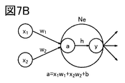
- FIG. 7B shows an example of calculation by neurons.
- two neurons in the presheaf layer that output a signal to the neuron Ne and a neuron Ne are shown.
- the output x 1 of the presheaf neuron and the output x 2 of the presheaf neuron are input to the neuron Ne.
- the neuron Ne the sum of the multiplication result of the output x 1 and the weight w 1 (x 1 w 1 ) and the multiplication result of the output x 2 and the weight w 2 (x 2 w 2 ) is x 1 w 1 + x 2 w 2.
- the calculation by the neurons includes the calculation of adding the product of the output of the neurons in the previous layer and the weight, that is, the sum-of-products operation (x 1 w 1 + x 2 w 2 above ).
- This product-sum operation may be performed by software using a program or by hardware.
- the product-sum calculation is performed using an analog circuit as hardware.
- an analog circuit is used for the product-sum calculation circuit, the processing speed can be improved and the power consumption can be reduced by reducing the circuit scale of the product-sum calculation circuit or reducing the number of times the memory is accessed.
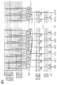
- FIG. 8 is an example of a circuit that can be used for the circuit 304.
- the circuit is a shift register circuit, and a plurality of logic circuits (SR) are electrically connected.
- Signal lines such as wiring RES, wiring VSS_RDRS, wiring RPWC_SE [0: 3], wiring RCLK [0: 3], and wiring RSP are connected to each logic circuit (SR), and appropriate signals are connected to each signal line.
- the selected signal potential can be sequentially output from the logic circuit (SR).
- the circuit 170 is electrically connected to the logic circuit (SR).
- a plurality of transistors are provided in the circuit 170, signal lines such as wiring SE_SW [0: 2] and wiring SX [0: 2] are connected, and an appropriate signal potential is input to each signal line to connect the transistors. Continuity is controlled. By controlling the circuit 170, the number of rows of selected pixels can be switched.
- One of the source or drain of one transistor is electrically connected to the output terminal of one logic circuit (SR), and the wiring SE is connected to the other of the source or drain of the transistor.
- the wiring SE is electrically connected to the wiring 122 that selects the pixel 100.
- the signal potential supplied from the wiring SE_SW [0] can be input to the gate of the transistor connected to the wiring SE [0].
- the signal potential supplied from the wiring SE_SW [1] can be input to the gate of the transistor connected to the wiring SE [1].
- the signal potential supplied from the wiring SE_SW [2] can be input to the gate of the transistor connected to the wiring SE [2].
- a signal potential supplied from any of the wiring SE_SW [0: 2] can be input to the gate of the transistor connected after the wiring SE [3] in the same order.
- the adjacent wiring SEs are electrically connected via one transistor, and the wiring SE [0] is electrically connected to the power supply line (VSS) via one transistor.
- the signal potential supplied from the wiring SX [0] can be input to the gate of the transistor that electrically connects the power supply line (VSS) and the wiring SE [0].
- the signal potential supplied from the wiring SX [1] can be input to the gate of the transistor that electrically connects the wiring SE [0] and the wiring SE [1].
- the signal potential supplied from the wiring SX [2] can be input to the gate of the transistor that electrically connects the wiring SE [1] and the wiring SE [2]. Any of the signal potentials supplied from the wiring SE_SX [0: 2] can be input to the gate of the transistor that electrically connects the wiring SEs thereafter in the same order.
- FIG. 9 is a timing chart illustrating an operation of simultaneously selecting a plurality of rows (3 rows) by the circuit shown in FIG. (0) to (161) correspond to the timing at which the logic circuit (SR) outputs the signal potential to the wiring SE.
- the potential of the wiring SX [0] is “L”
- the potential of the wiring SX [1] is “H”
- the potential of the wiring SX [2] is "H”
- the potential of the wiring SE_SW [0] is.
- 3 rows can be selected at the same time, and for example, a product-sum operation of 3 rows and 3 columns of pixels can be performed.
- the potential of the wiring SX [0] is “H”
- the potential of the wiring SX [1] is “L”
- the potential of the wiring SX [2] is "H”
- the potential of the wiring SE_SW [0] is.
- the continuity of each transistor is controlled, and wiring SE [0] becomes “L”
- wiring SE. “H” is output to [1]
- “H” is output to wiring SE [2]
- “H” is output to wiring SE [3].
- “L” is output to the other wiring SEs.
- FIG. 10 is a timing chart illustrating an operation of selecting one row by the circuit shown in FIG.
- a rolling shutter method and a global shutter method will be described as an example of an imaging method that can be used in the imaging device of one aspect of the present invention.
- FIG. 11A is a diagram illustrating the operation method of the rolling shutter system
- FIG. 11B is a diagram illustrating the global shutter system.
- En represents the exposure (accumulation operation) of the nth column (n is a natural number)
- Rn represents the reading operation of the nth column.
- FIGS. 11A and 11B the operations from the first row to the Mth row (M is a natural number) are shown.
- the rolling shutter method is an operation method in which exposure and data reading are performed in sequence, and is a method in which the reading period of one line and the exposure period of another line are overlapped. Since the reading operation is performed immediately after the exposure, imaging can be performed even with a circuit configuration having a relatively short data retention period. Since one frame of an image is composed of data that are not simultaneously captured, the image is likely to be distorted when capturing a moving object.
- the global shutter method is an operation method in which all pixels are exposed at the same time, data is held in each pixel, and data is read out row by row. Therefore, it is possible to obtain an image without distortion even when imaging a moving object.
- the image pickup apparatus of one aspect of the present invention can extremely reduce the fluctuation of the data potential accumulated in the pixel by exposure by increasing the capacitance value of the capacitor such as the capacitor 104 shown in FIGS. 3A and 3B. Since the data retention time can be lengthened, the global shutter method can be easily realized.
- the imaging device according to one aspect of the present invention can also be operated by the rolling shutter method.
- Line [m] (m is a natural number of 1 or more and M or less) is the m-th row of the pixel 100
- En is the exposure of the n-th column of the pixel 100
- Rn is the n-th column of the pixel 100.
- Line [m] (m is a natural number of 1 or more and M or less) is the m-th row of the pixel block 200
- En is the exposure of the nth column of the pixel block 200
- Rn is the pixel block.
- the reading operation of the nth column of 200 may be pointed out respectively.
- the imaging device of one aspect of the present invention may have the pixels shown in FIG. 11C.
- the pixel shown in FIG. 11C includes a photoelectric conversion device 101, a transistor 102, a transistor 103, a capacitor 171 and a capacitor 150, a transistor 105, a transistor 108, and a transistor 172.
- the signal from the photoelectric conversion device 101 is given to one of the source or drain of the transistor 102, and the other of the source or drain of the transistor 102 is electrically connected to one of the source or drain of the transistor 103 and the node N2.
- the other of the source or drain of the transistor 103 is electrically connected to the wiring 115, the node N2 is electrically connected to one electrode of the capacitor 171 and the other electrode of the capacitor 171 is electrically connected to the node N. Be connected.
- the gate of the transistor 102 is electrically connected to the wiring 116
- the gate of the transistor 103 is electrically connected to the wiring 117
- the gate of the transistor 105 is electrically connected to the node N
- the gate of the transistor 108 is.
- the gate of the transistor 172 is electrically connected to the wiring 173.
- the node N is electrically connected to one electrode of the capacitor 150, the gate of the transistor 105, and one of the source or drain of the transistor 172.
- a signal for turning on the transistor 102 is given from the wiring 116 to the gate of the transistor 102, and a signal from the photoelectric conversion device 101 is given to the node N2.
- the potential of node N2 changes according to the given signal and becomes the potential V1 [V].
- a signal for turning on the transistor 172 is given from the wiring 173 to the gate of the transistor 172, and a reference potential is given to the node N.
- 0 [V] is given as the reference potential.
- a signal for turning off the transistor 102 is given from the wiring 116 to the gate of the transistor 102
- a signal for turning off the transistor 172 is given from the wiring 173 to the gate of the transistor 172
- the transistor 103 is turned on.
- the signal to be used is given from the wiring 117 to the gate of the transistor 103
- a reference potential is given to the node N2.
- VDD [V] is given as the reference potential
- the potential of the node N2 rises from the potential V1 [V] to VDD [V].
- the potential of the node N In response to the change in the potential of the node N2, the potential of the node N also rises from 0 [V] to VDD-V1 [V] due to capacitive coupling.
- a signal for turning off the transistor 103 is given from the wiring 117 to the gate of the transistor 103, a signal for turning off the transistor 172 is given from the wiring 173 to the gate of the transistor 172, and the transistor 102 is turned on.
- the signal to be used is given from the wiring 116 to the gate of the transistor 102, and the signal from the photoelectric conversion device 101 is given to the node N2.
- the potential of node N2 becomes the potential V2 [V].
- Capacitive coupling causes the potential of node N to drop to (V2-V1) [V]. That is, the node N is given a difference between the signal from the photoelectric conversion device 101 at the first time and the signal from the photoelectric conversion device 101 at the third time.
- the difference between the signals at the two times can be calculated and output.
- Motion detection can be performed by comparing the two images with the image captured at the first time as the reference image and the image captured at the third time as the comparison image.
- FIG. 12A and 12B show examples of the pixel structure of the image pickup apparatus.
- the pixel shown in FIG. 12A is an example of a laminated structure of layers 502 and 503.
- the layer 502 has a pixel 100 and a photoelectric conversion device 101.
- Layer 503 also has an optical conversion layer and a microlens array.
- the photoelectric conversion device 101 can be laminated with the layer 565a and the layer 565b as shown in FIG. 12C.
- the photoelectric conversion device 101 shown in FIG. 12C is a pn junction type photodiode.
- a p-type semiconductor can be used for the layer 565a and an n-type semiconductor can be used for the layer 565b.
- an n-type semiconductor may be used for the layer 565a and a p-type semiconductor may be used for the layer 565b.
- the photoelectric conversion device 101 can be laminated with the layer 565a, the layer 565b, and the layer 565c as shown in FIG. 12D.
- the photoelectric conversion device 101 shown in FIG. 12D is a pn junction type photodiode.
- a p-type semiconductor can be used for the layer 565a and an n-type semiconductor can be used for the layer 565b.
- a pn junction photodiode can be formed by laminating layers 565a and 565b.
- a p-type semiconductor can be used for the layer 565c.
- surface scattering may be suppressed.
- an n-type semiconductor may be used for the layer 565a, a p-type semiconductor for the layer 565b, and an n-type semiconductor for the layer 565c.
- the photoelectric conversion device may be a pin junction type photodiode in which a layer 565d, which is an i-type semiconductor, is provided between the layers 565a and 565b.
- the pn junction type photodiode or the pin junction type photodiode can be formed by using single crystal silicon. Further, as the pin junction type photodiode, a thin film such as amorphous silicon, microcrystalline silicon, or polycrystalline silicon can be used to form the photodiode.
- the photoelectric conversion device 101 included in the layer 502 may be a laminate of the layer 566a, the layer 566b, the layer 566c, and the layer 566d.
- the photoelectric conversion device 101 shown in FIG. 12F is an example of an avalanche photodiode, in which layers 566a and 566d correspond to electrodes, and layers 566b and 566c correspond to photoelectric conversion units.
- the layer 566a is preferably a low resistance metal layer or the like.
- a low resistance metal layer or the like aluminum, titanium, tungsten, tantalum, silver or a laminate thereof can be used.
- the layer 566d it is preferable to use a conductive layer having high translucency with respect to visible light.
- a conductive layer having high translucency with respect to visible light For example, indium oxide, tin oxide, zinc oxide, indium-tin oxide, gallium-zinc oxide, indium-gallium-zinc oxide, graphene and the like can be used. It should be noted that the layer 566d may be omitted.
- a silicon substrate can be used as the layer 502 shown in FIG. 12A.
- the silicon substrate has a Si transistor and the like.
- the Si transistor can be used to provide a circuit for driving the pixel circuit, an image signal readout circuit, an image processing circuit, a storage circuit, and the like.
- some or all the transistors of the circuits 201, 301, 302, 303, 304 and 305 described in the first embodiment can be provided on the layer 502.
- the pixel may have a laminated structure of layers 501, 502 and 503 as shown in FIG. 12B.
- Layer 501 can have a capacitor that pixel 100 has.
- the area of the image pickup apparatus can be reduced by providing the capacitor 104 on the layer 501. Further, if the manufacturing process of the capacitor 104 and the manufacturing process of the transistor included in the pixel 100 can be separated, the imaging device may be manufactured at a lower cost.
- the layer 501 can have a part of semiconductor elements such as a transistor and a capacitor of the pixel 100 in addition to the capacitor 104.
- the ratio of the area of the photoelectric conversion device 101 to the area of the pixel in the layer 502 can be increased. Therefore, the sensitivity of the image pickup apparatus may be further increased. In addition, the resolution of the imaging device may be increased.
- Layer 501 may also have some or all of the transistors included in circuits 201, 301, 302, 303, 304 and 305.
- the elements and peripheral circuits constituting the pixel circuit can be dispersed in a plurality of layers, and the elements can be provided with each other or the elements and the peripheral circuits can be overlapped with each other, so that the area of the imaging device can be reduced. be able to.
- the layer 501 may be used as a support substrate, and a peripheral circuit may be provided on the layer 502.
- FIG. 13A is an example of a cross-sectional view of a laminate having a layer 502 and a layer 503.
- Layer 502 has pixels 100 formed on a silicon substrate.
- the transistor 102, the transistor 103, the capacitor 104, the capacitor 150, and the photoelectric conversion device 101 are shown as a part of the pixel 100.
- the photoelectric conversion device 101 is a pn junction type photodiode formed on a silicon substrate, and has a p-type region 243 and an n-type region 244.
- the photoelectric conversion device 101 is an embedded photodiode, and a p-type region 241 provided on the surface side of the n-type region 244 can suppress dark current and reduce noise.
- the p-type region 243 may be used as the p-type region 241.
- the resistance of the p-type region 241 is preferably lower than that of the p-type region 243. Further, it is preferable that the resistance of the n-type region 244 is lower than that of the p-type region 243. Further, in the p-type region 243, the p-type region 241 and the n-type region 244, the p-type region and the n-type region may be exchanged.
- the transistor 102 and the transistor 103 are transistors formed on a silicon substrate.
- the transistors 102 and 103 have a conductive layer that functions as a gate, a source, a drain, and a channel forming region located between the source and the drain formed on the silicon substrate, and a conductive layer and a channel forming region that function as a gate. It has a gate insulating layer provided between the two.
- the source region and the drain region of the transistor 102 and the transistor 103 are formed by an n-type region.
- the layer 502 is provided with an insulating layer 242 and an insulating layer 245.
- the insulating layer 242 has a function as an element separation layer.
- the insulating layer 245 has a function of suppressing the outflow of carriers.
- the silicon substrate is provided with a groove for separating pixels, and the insulating layer 245 is provided on the upper surface of the silicon substrate and the groove.
- the insulating layer 245 By providing the insulating layer 245, it is possible to prevent the carriers generated in the photoelectric conversion device 101 from flowing out to the adjacent pixels.
- the insulating layer 245 also has a function of suppressing the intrusion of stray light. For example, when the insulating layer 245 has a groove, the intrusion of stray light from adjacent pixels may be suppressed. Therefore, the insulating layer 245 can suppress color mixing.
- An antireflection film may be provided between the upper surface of the silicon substrate and the insulating layer 245.
- the element separation layer can be formed by using a LOCOS (LOCOS Exidation of Silicon) method, an STI (Shallow Trench Isolation) method, or the like.
- LOCOS LOCOS Exidation of Silicon
- STI Shallow Trench Isolation
- the insulating layer 245 for example, a silicon oxide film, an inorganic insulating film such as silicon nitride, or an organic insulating film such as polyimide or acrylic can be used.
- the insulating layer 245 may have a multi-layer structure.
- the n-type region 244 (corresponding to the cathode) of the photoelectric conversion device 101 can also function as either the source or the drain of the transistor 102.
- the layer 502 is provided with insulating layers 222, 223, 226, 227, and wiring 121.
- the insulating layer 222 has a function as a protective film.
- the insulating layers 223 and 227 have functions as an interlayer insulating film and a flattening film.
- the insulating layer 226 has a function as a dielectric layer of the capacitor 150.
- the wiring 121 has a function as a power supply line.
- the p-type region 243 (anode) is electrically connected to the wiring 121.
- a silicon nitride film, a silicon oxide film, an aluminum oxide film, or the like can be used as the protective film.
- an inorganic insulating film such as a silicon oxide film or an organic insulating film such as an acrylic resin or a polyimide resin can be used.
- a silicon nitride film, a silicon oxide film, an aluminum oxide film, or the like can be used as the dielectric layer of the capacitor.
- the Si transistor shown in FIG. 13A is a planar type having a channel forming region on a silicon substrate.
- the Si transistor may be a fin type as shown in FIG. 18A.
- FIG. 18B shows a cross section (cross section in the channel width direction) of A1-A2 shown in FIG. 18A.
- the semiconductor layer 545 can be, for example, single crystal silicon (SOI (Silicon on Insulator)) formed on the insulating layer 546 on the silicon substrate 210.
- SOI Silicon on Insulator
- Conductors that can be used as wiring, electrodes, and plugs for electrical connections between devices include aluminum, chromium, copper, silver, gold, platinum, tantalum, nickel, titanium, molybdenum, tungsten, and hafnium. , Vanadium, niobium, manganese, magnesium, zirconium, beryllium, indium, ruthenium, iridium, strontium, lanthanum, etc., or alloys containing the above-mentioned metal elements as components, or alloys containing the above-mentioned metal elements. Etc. may be appropriately selected and used.
- the conductor is not limited to a single layer, and may be a plurality of layers made of different materials.
- the capacitor 104 is a trench capacitor provided on a silicon substrate.
- the capacitor 104 shown in FIG. 13A is formed between the trench formed in the p-type region 243 of the silicon substrate, the conductive layer 151 formed so as to embed the inside of the trench, and the p-type region 243 and the conductive layer 151. It has an insulating layer 152.
- the p-type region 243 and the conductive layer 151 have a function as electrodes of the capacitor 104.
- the aspect ratio of the trench formed on the silicon substrate is, for example, preferably 10 or more, and more preferably 20 or more. By increasing the aspect ratio, the capacitance value with respect to the circuit area can be increased.
- the aspect ratio of the trench is the value obtained by dividing the depth of the trench by the diameter of the upper part of the trench.
- the film thickness of the insulating layer 152 is, for example, preferably 20 nm or less, more preferably 15 nm or less, and even more preferably 10 nm or less. By reducing the film thickness of the insulating layer 152, the capacitance value of the capacitor 104 can be increased. On the other hand, when the insulating layer 152 has a certain thickness, the variation between the elements may be reduced. Therefore, the thickness of the insulating layer 152 is, for example, 1 nm or more, or 2 nm or more.
- the conductive layer 151 for example, the above-mentioned materials and configurations can be used as the conductor that can be used as wiring, electrodes, and plugs. Further, as the conductive layer 151, polycrystalline silicon doped with impurities such as phosphorus and boron can be used in order to reduce the resistance.
- the insulating layer 152 can function as a dielectric of the capacitor 104.
- As the insulating layer 152 for example, it is preferable to use a thermal oxide film obtained by oxidizing the surface of a trench formed on a silicon substrate.
- the dielectric preferably has one or more selected from silicon oxide, aluminum oxide, hafnium oxide and zirconium oxide. Further, it may have a laminated structure of these materials.
- the dielectric may have an oxide having one or more selected from silicon, aluminum, titanium, lead, barium, strontium, barium, zirconium and bismuth.
- it may have strontium titanate, barium titanate, strontium titanate and the like. Further, it may have a laminated structure of these oxides.
- FIG. 13B shows an example in which the configurations of the capacitor 104 are different from those of FIG. 13A. Note that in FIG. 13B, the details of the layer 503 are not shown for the sake of simplicity.
- FIG. 13B shows an example in which an n-type region is provided on the surface of a trench provided on a silicon substrate in a capacitor 104. In the capacitor 104 shown in FIG. 13B, the n-type region provided on the surface of the trench and the conductive layer 151 have functions as electrodes of the capacitor 104.
- the n-type region provided on the surface of the trench preferably has a lower resistance than the p-type region 243.
- the capacitor 150 has a conductive layer 123 and a conductive layer 124 provided so as to sandwich the insulating layer 226.
- the conductive layer 123 and the conductive layer 124 have a function as electrodes of the capacitor 150.
- the conductive layer 123 is electrically connected to the other of the source or drain of the transistor 102 and one of the source or drain of the transistor 103 via the conductive layer formed in the insulating layer 223.
- capacitors 104 and 150 may be interchanged in FIGS. 13A, 13B and 14 described later.
- Layer 503 is formed on layer 502.
- the layer 503 includes a light-shielding layer 251, an optical conversion layer 250, and a microlens array 255.
- the light-shielding layer 251 can suppress the inflow of light to adjacent pixels.
- a metal layer such as aluminum or tungsten can be used for the light-shielding layer 251. Further, the metal layer and a dielectric film having a function as an antireflection film may be laminated.
- a color filter can be used for the optical conversion layer 250.
- a color image can be obtained by assigning colors such as R (red), G (green), B (blue), Y (yellow), C (cyan), and M (magenta) to the color filter for each pixel.
- a wavelength cut filter is used for the optical conversion layer 250, it can be used as an image pickup device that can obtain images in various wavelength regions.
- the optical conversion layer 250 uses a filter that blocks light below the visible light wavelength, it can be used as an infrared imaging device. Further, if the optical conversion layer 250 uses a filter that blocks light having a wavelength of near infrared rays or less, a far infrared ray imaging device can be obtained. Further, if the optical conversion layer 250 uses a filter that blocks light having a wavelength equal to or higher than that of visible light, it can be used as an ultraviolet imaging device.
- a scintillator is used for the optical conversion layer 250, it can be used as an imaging device for obtaining an image that visualizes the intensity of radiation used in an X-ray imaging device or the like.
- radiation such as X-rays transmitted through a subject
- a scintillator it is converted into light (fluorescence) such as visible light or ultraviolet light by a photoluminescence phenomenon.
- the image data is acquired by detecting the light with the photoelectric conversion device 101.
- an imaging device having the above configuration may be used as a radiation detector or the like.
- the scintillator contains a substance that absorbs the energy and emits visible light or ultraviolet light when irradiated with radiation such as X-rays and gamma rays.
- Gd 2 O 2 S Tb
- Gd 2 O 2 S Pr
- Gd 2 O 2 S Eu
- BaFCl Eu
- NaI, CsI, CaF 2 , BaF 2 , CeF 3 LiF, LiI, ZnO, etc.
- Those dispersed in resin or ceramics can be used.
- a microlens array 255 is provided on the optical conversion layer 250. Light passing through the individual lenses of the microlens array 255 passes through the optical conversion layer 250 directly below and is irradiated to the photoelectric conversion device 101. By providing the microlens array 255, the focused light can be incident on the photoelectric conversion device 101, so that photoelectric conversion can be performed efficiently.
- the microlens array 255 is preferably formed of a resin or glass having high translucency with respect to visible light.
- FIG. 14 shows a configuration example different from that of FIG. 13B.
- the laminated structure shown in FIG. 14 is an example of a cross-sectional view of a laminated body having layers 501 to 503 and having a bonding surface between the layers 501 and 502.
- FIG. 14 is different from FIG. 13B in that it has an insulating layer 231 and a conductive layer 132, a layer 501, and a capacitor 104 is provided in a layer different from that of FIG. 13B.
- FIG. 13 shows an example in which the capacitor 104 is provided in the layer 502, but
- FIG. 14 shows an example in which the capacitor 104 is provided in the layer 501.
- the layer 502 shown in FIG. 14 has an insulating layer 231 and a conductive layer 132.
- the insulating layer 231 and the conductive layer 132 have a function as a bonding layer.
- the conductive layer 132 is electrically connected to the conductive layer 123.
- the layer 501 shown in FIG. 14 has a silicon substrate 153 and a capacitor 104.
- the capacitor 104 is a trench capacitor provided on a silicon substrate.
- the capacitor 104 shown in FIG. 14 has an n-type region 154 formed near the surface layer of a trench formed on a silicon substrate 153, a conductive layer 155 formed so as to be embedded in the trench, and an n-type region and a conductive layer 155. It has an insulating layer 156 formed between the two.
- the n-type region 154 and the conductive layer 155 have a function as electrodes of the capacitor 104.
- the insulating layer 156 has a function as a dielectric layer of the capacitor 104.
- the conductive layer 151 and the insulating layer 152 can be referred to.
- the insulating layer 156 can be formed, for example, by thermal oxidation of silicon. By forming an insulating film obtained by thermal oxidation of silicon, a dense thin film having a uniform thickness can be obtained. By using thermal oxidation of silicon, a thinner insulating film can be easily and stably produced, which is suitable for producing a capacitor 104 having a high capacitance value.
- the layer 501 has an insulating layer 222b formed on the silicon substrate 153 and the conductive layer 155, an insulating layer 223b, an insulating layer 227b, an insulating layer 229, a conductive layer 158, and a conductive layer 131. ..
- the insulating layers 222b, 223b, and 227b have functions as an interlayer insulating film and a flattening film.
- the insulating layer 229 and the conductive layer 131 have a function as a bonding layer.
- the conductive layer 131 is electrically connected to the conductive layer 155 via the conductive layer 158 formed in the insulating layer 227b and the conductive layer formed in the insulating layer 223b.
- FIG. 15 shows an example in which layer 501 has transistors.
- the laminated structure shown in FIG. 15 has layers 501 to 503, and has a bonding surface between the layers 501 and 502.
- layer 501 has a capacitor 104 and a transistor 106
- layer 502 has a transistor 102, a transistor 103, a photoelectric conversion device 101 and a capacitor 150
- layer 503 has an optical conversion layer 250.
- the layer 502 may be configured not to have the capacitor 150.
- FIG. 16A shows an example of FIG. 15 without the capacitor 150.
- the transistor 106 shown in FIG. 15 has a conductive layer 263 that can function as a gate, and an n-type region 264 and an n-type region 265 that can function as a source region on one side and a drain region on the other side.
- the capacitor 104 shown in FIG. 15 has a conductive layer 261 on the conductive layer 155 in addition to the capacitor 104 shown in FIG.
- the conductive layer 155 and the conductive layer 261 are electrically connected. Further, the conductive layer 261 and the conductive layer 263 may be formed by using the same process.
- the n-type region 265 is electrically connected to the conductive layer 262 on the insulating layer 223b via a conductive layer formed so as to be embedded in the insulating layer 222b and the insulating layer 223b.
- the conductive layer 262 functions as, for example, wiring 111. Alternatively, for example, the conductive layer 262 is electrically connected to the wiring 111.
- a p-type region can be used for the channel formation region of the transistor 106.
- the resistance of the n-type regions 264, 265 and 154 is preferably lower than that of the p-type region.
- the p-type region used for the channel region or the like of the transistor 106 may be replaced with the n-type region, and the n-type regions 264, 265 and 154 may be replaced with the p-type region.
- the number of transistors arranged in the layer 502 can be reduced, and the ratio of the area of the photoelectric conversion device 101 shown in the pixel area can be increased. it can. Therefore, the sensitivity of the image pickup apparatus according to one aspect of the present invention can be increased. Further, the resolution of the image pickup apparatus according to one aspect of the present invention can be increased.
- the n-type region 264 and the n-type region 154 are in contact with each other, so that the configuration can be continuous. Therefore, the distance between the elements of the transistor 106 and the capacitor 104 can be reduced, and the circuit can be integrated.
- the configuration shown in FIG. 16B may be used as the configuration of the capacitor 104.
- the conductive layer 155 of the capacitor 104 is in contact with the n-type region 264 of the transistor 106 in a shallow trench region.
- the n-type region 154 may not be provided.
- the conductive layer 158 is preferably electrically connected to the substrate potential of the silicon substrate 153.
- FIG. 17A shows an example in which layer 501 has transistors 105 in addition to the structure shown in FIG. 16A.
- the transistor 105 is a transistor formed on the silicon substrate 153.
- the conductive layer 266 included in the transistor 105 can function as a gate of the transistor 105.
- the conductive layer 266 is electrically connected to the conductive layer 261 via the conductive layer 158.
- FIG. 17B shows an example in which the layer 502 has a transistor 105 in addition to the structure shown in FIG. 16A.
- the transistor 105 is a transistor formed on a silicon substrate.
- the conductive layer 267 included in the transistor 105 can function as a gate of the transistor 105.
- the conductive layer 267 is electrically connected to the other of the source or drain of the transistor 102 and one of the source or drain of the transistor 103 via a conductive layer or the like formed in the insulating layer 223.
- the configurations shown in FIGS. 13A, 13B, 14, 15, 16A, 16B, 17A, and 17B may be applied to the transistors and capacitors included in the pixels shown in FIG. 11C.
- the configuration of the capacitor 104 may be applied to the capacitor 171.
- the configuration of the transistor 106 may be applied to the transistor 172.
- the layer 501 is provided with an insulating layer 229 and a conductive layer 131.
- the conductive layer 131 has a region embedded in the insulating layer 229. Further, the surfaces of the insulating layer 229 and the conductive layer 131 are flattened so that their heights match.
- the layer 502 is provided with an insulating layer 231 and a conductive layer 132.
- the conductive layer 132 has a region embedded in the insulating layer 231. Further, the surfaces of the insulating layer 231 and the conductive layer 132 are flattened so that their heights match.
- the conductive layer 131 and the conductive layer 132 are metal elements having the same main components. Further, it is preferable that the insulating layer 229 and the insulating layer 231 are composed of the same components.
- Cu, Al, Sn, Zn, W, Ag, Pt, Au, or the like can be used for the conductive layers 131 and 132.
- Cu, Al, W, or Au is preferably used because of the ease of joining.
- silicon oxide, silicon oxide nitride, silicon nitride oxide, silicon nitride, titanium nitride and the like can be used for the insulating layer 229 and 231.
- the conductive layer 131 and the conductive layer 132 may have a multi-layer structure of a plurality of layers, in which case, the surface layer (bonding surface) may be the same metal material. Further, the insulating layer 229 and the insulating layer 231 may also have a multilayer structure of a plurality of layers, and in that case, the insulating material may have the same surface layer (bonding surface).
- the electrical connection between the conductive layer 131 and the conductive layer 132 can be satisfactorily obtained. Further, it is possible to obtain a connection having sufficient mechanical strength of the insulating layer 229 and the insulating layer 231.
- a surface activation bonding method can be used in which the oxide film on the surface and the adsorption layer of impurities are removed by sputtering or the like, and the cleaned and activated surfaces are brought into contact with each other for bonding. ..
- a diffusion bonding method or the like in which surfaces are bonded to each other by using both temperature and pressure can be used. Since bonds occur at the atomic level in both cases, excellent bonding can be obtained not only electrically but also mechanically.
- the surfaces treated with hydrophilicity such as oxygen plasma are brought into contact with each other for temporary bonding, and then main bonding is performed by dehydration by heat treatment.
- a joining method or the like can be used. Since the hydrophilic bonding method also causes bonding at the atomic level, it is possible to obtain mechanically excellent bonding.
- an insulating layer and a metal layer are mixed on each bonding surface, so that, for example, a surface activation bonding method and a hydrophilic bonding method may be combined.
- a method can be used in which the surface is cleaned after polishing, the surface of the metal layer is subjected to an antioxidant treatment, and then a hydrophilic treatment is performed to join the metal layer.
- the surface of the metal layer may be made of a refractory metal such as Au and subjected to hydrophilic treatment.
- a joining method other than the above-mentioned method may be used.
- the transistor 102, the transistor 103, the capacitor 150 and the like of the layer 502 can be electrically connected to the capacitor 104 of the layer 501.
- FIG. 19A is an external perspective view of the upper surface side of the package containing the image sensor chip.
- the package has a package substrate 610 for fixing the image sensor chip 650, a cover glass 620, an adhesive 630 for adhering both, and the like.
- FIG. 19B is an external perspective view of the lower surface side of the package.
- the lower surface of the package has a BGA (Ball grid array) in which solder balls are bumps 640.
- BGA Ball grid array
- LGA Land grid array
- PGA Peripheral Component Interconnect
- FIG. 19C is a perspective view of the package shown by omitting a part of the cover glass 620 and the adhesive 630.
- An electrode pad 660 is formed on the package substrate 610, and the electrode pad 660 and the bump 640 are electrically connected via a through hole.
- the electrode pad 660 is electrically connected to the image sensor chip 650 by a wire 670.
- FIG. 19D is an external perspective view of the upper surface side of the camera module in which the image sensor chip is housed in a lens-integrated package.
- the camera module has a package substrate 611 for fixing the image sensor chip 651, a lens cover 621, a lens 635, and the like.
- an IC chip 690 having functions such as a drive circuit for an image pickup device and a signal conversion circuit is also provided between the package substrate 611 and the image sensor chip 651, and has a configuration as a SiP (System in package). There is.
- FIG. 19E is an external perspective view of the lower surface side of the camera module.
- the lower surface and the side surface of the package substrate 611 have a QFN (Quad flat no-lead package) configuration in which a land 641 for mounting is provided.
- the configuration is an example, and a QFP (Quad flat package) or the above-mentioned BGA may be provided.
- FIG. 19F is a perspective view of the module shown by omitting a part of the lens cover 621 and the lens 635.
- the land 641 is electrically connected to the electrode pad 661, and the electrode pad 661 is electrically connected to the image sensor chip 651 or the IC chip 690 by a wire 671.
- the image sensor chip By housing the image sensor chip in the above-mentioned package, it becomes easy to mount it on a printed circuit board or the like, and the image sensor chip can be incorporated into various semiconductor devices and electronic devices.
- Electronic devices that can use the imaging device according to one aspect of the present invention include a display device, a personal computer, an image storage device or image reproduction device provided with a recording medium, a mobile phone, a game machine including a portable type, and a portable data terminal.
- Electronic book terminals video cameras, cameras such as digital still cameras, goggles type displays (head mount displays), navigation systems, sound reproduction devices (car audio, digital audio players, etc.), copiers, facsimiles, printers, multifunction printers , Automatic cash deposit / payment machines (ATMs), vending machines, etc. Specific examples of these electronic devices are shown in FIGS. 20A to 20F.
- FIG. 20A is an example of a mobile phone, which includes a housing 981, a display unit 982, an operation button 983, an external connection port 984, a speaker 985, a microphone 986, a camera 987, and the like.
- the mobile phone includes a touch sensor on the display unit 982. All operations such as making a phone call or inputting characters can be performed by touching the display unit 982 with a finger or a stylus.
- An image pickup device according to an aspect of the present invention and an operation method thereof can be applied to an element for image acquisition in the mobile phone.
- FIG. 20B is a portable data terminal, which includes a housing 911, a display unit 912, a speaker 913, a camera 919, and the like.
- Information can be input and output by the touch panel function of the display unit 912.
- characters and the like can be recognized from the image acquired by the camera 919, and the characters can be output as voice by the speaker 913.
- An image pickup device according to an aspect of the present invention and an operation method thereof can be applied to an element for image acquisition in the portable data terminal.
- FIG. 20C is a surveillance camera, which has a support base 951, a camera unit 952, a protective cover 953, and the like.
- the camera unit 952 is provided with a rotation mechanism or the like, and by installing it on the ceiling, it is possible to take an image of the entire surroundings.
- An image pickup apparatus according to an aspect of the present invention and an operation method thereof can be applied to an element for image acquisition in the camera unit.
- the surveillance camera is a conventional name and does not limit its use.
- a device having a function as a surveillance camera is also called a camera or a video camera.
- FIG. 20D is a video camera, which includes a first housing 971, a second housing 972, a display unit 973, an operation key 974, a lens 975, a connection unit 976, a speaker 977, a microphone 978, and the like.
- the operation key 974 and the lens 975 are provided in the first housing 971, and the display unit 973 is provided in the second housing 972.
- An image pickup apparatus according to an aspect of the present invention and an operation method thereof can be applied to an element for image acquisition in the video camera.
- FIG. 20E is a digital camera, which includes a housing 961, a shutter button 962, a microphone 963, a light emitting unit 967, a lens 965, and the like.
- An image pickup apparatus according to an aspect of the present invention and an operation method thereof can be applied to an element for image acquisition in the digital camera.
- FIG. 20F is a wristwatch-type information terminal, which has a display unit 932, a housing / wristband 933, a camera 939, and the like.
- the display unit 932 includes a touch panel for operating the information terminal.
- the display unit 932 and the housing / wristband 933 have flexibility and are excellent in wearability to the body.
- An image pickup apparatus according to an aspect of the present invention and an operation method thereof can be applied to an element for image acquisition in the information terminal.
Landscapes
- Engineering & Computer Science (AREA)
- Multimedia (AREA)
- Signal Processing (AREA)
- Human Computer Interaction (AREA)
- Solid State Image Pick-Up Elements (AREA)
- Transforming Light Signals Into Electric Signals (AREA)
- Thin Film Transistor (AREA)
Abstract
Description
図2は、画素ブロック200および回路201を説明する図である。
図3A、図3Bは、画素100を説明する図である。
図4A、図4Bは、画素ブロック200および回路201の動作を説明するタイミングチャートである。
図5A、図5Bは、回路301および回路302を説明する図である。
図6は、回路302が有する画素を説明する図である。
図7A、図7Bは、ニューラルネットワークの構成例を示す図である。
図8は、回路304を説明する図である。
図9は、回路304の動作を説明するタイミングチャートである。
図10は、回路304の動作を説明するタイミングチャートである。
図11Aは、ローリングシャッタの動作を説明する図である。図11Bは、グローバルシャッタの動作を説明する図である。図11Cは画素の一例である。
図12A乃至Fは、撮像装置の画素の構成を説明する図である。
図13Aは、画素を説明する断面図である。図13Bは、画素を説明する断面図である。
図14は、画素を説明する断面図である。
図15は、画素を説明する断面図である。
図16Aは、画素を説明する断面図である。図16Bは、画素を説明する断面図である。
図17Aは、画素を説明する断面図である。図17Bは、画素を説明する断面図である。
図18A乃至Cは、Siトランジスタを説明する図である。
図19A乃至Fは、撮像装置を収めたパッケージ、モジュールの斜視図である。
図20A乃至Fは、電子機器を説明する図である。
本実施の形態では、本発明の一態様である撮像装置について、図面を参照して説明する。
本実施の形態では、本発明の一態様の撮像装置の構造例などについて説明する。
次に、撮像装置の積層構造について、断面図を用いて説明する。
層502は、シリコン基板に形成された画素100を有する。ここでは、画素100の一部として、トランジスタ102、トランジスタ103、キャパシタ104、キャパシタ150および光電変換デバイス101を示している。
層503は、層502上に形成される。層503は、遮光層251、光学変換層250およびマイクロレンズアレイ255を有する。
図14は、図13Bとは異なる構成例を示す。
図14に示す層501は、シリコン基板153と、キャパシタ104と、を有する。キャパシタ104は、シリコン基板に設けられたトレンチキャパシタである。図14に示すキャパシタ104は、シリコン基板153に形成されるトレンチの表層近傍に形成されるn型領域154と、トレンチ内を埋め込むように形成される導電層155と、n型領域と導電層155の間に形成される絶縁層156と、を有する。n型領域154および導電層155は、キャパシタ104の電極としての機能を有する。絶縁層156は、キャパシタ104の誘電体層としての機能を有する。なお、図14に示すキャパシタ104において、n型領域154を設けない構成としてもよい。導電層155および絶縁層156に用いることができる材料、構成等について、導電層151および絶縁層152の記載を参照することができる。
図15には、層501がトランジスタを有する例を示す。
次に、層501と層502の貼り合わせについて、図14等を参照して説明する。
本実施の形態では、イメージセンサチップを収めたパッケージおよびカメラモジュールの一例について説明する。当該イメージセンサチップには、本発明の一態様の撮像装置の構成を用いることができる。
本発明の一態様に係る撮像装置を用いることができる電子機器として、表示機器、パーソナルコンピュータ、記録媒体を備えた画像記憶装置または画像再生装置、携帯電話、携帯型を含むゲーム機、携帯データ端末、電子書籍端末、ビデオカメラ、デジタルスチルカメラ等のカメラ、ゴーグル型ディスプレイ(ヘッドマウントディスプレイ)、ナビゲーションシステム、音響再生装置(カーオーディオ、デジタルオーディオプレイヤー等)、複写機、ファクシミリ、プリンタ、プリンタ複合機、現金自動預け入れ払い機(ATM)、自動販売機などが挙げられる。これら電子機器の具体例を図20A乃至図20Fに示す。
Claims (9)
- 画素ブロックと、第1の回路と、を有し、
前記画素ブロックは、マトリクス状に配置された複数の画素を有し、
前記画素ブロックと前記第1の回路は電気的に接続され、
前記複数の画素のそれぞれは、光電変換デバイスと、第1のトランジスタと、第2のトランジスタと、キャパシタと、を有し、
前記光電変換デバイスと前記第1のトランジスタは、第1の層に形成され、
前記キャパシタは、第2の層に形成され、
前記第2の層は、前記第1の層に接合され、
前記第1のトランジスタのソースまたはドレインの一方は前記光電変換デバイスの一方の電極と電気的に接続され、他方は前記キャパシタの一方の電極と電気的に接続され、
前記第2のトランジスタのソースまたはドレインの一方は前記キャパシタの他方の電極と電気的に接続され、
前記複数の画素のそれぞれは、第1のデータを生成する機能と、前記第1のデータを任意の倍率に乗算して第2のデータを生成する機能と、を有し、
前記第1の回路は、前記複数の画素のそれぞれが生成する前記第1のデータの和に相当する第3のデータを生成する機能と、前記複数の画素のそれぞれが生成する前記第2のデータの和に相当する電位を、容量結合により前記第3のデータに加算して第4のデータを生成する機能と、を有し、
前記第1のデータおよび前記第2のデータはアナログ値である撮像装置。 - 請求項1において、
前記第1のトランジスタおよび前記第2のトランジスタはそれぞれ、チャネル形成領域にシリコンを有する撮像装置。 - 請求項1または請求項2において、前記第1の層は、第1のシリコン基板上に形成され、
前記光電変換デバイスが有するn型領域と、前記第1のトランジスタのソースまたはドレインの一方と、が共有される撮像装置。 - 請求項1乃至請求項3のいずれか一において、
前記キャパシタはトレンチキャパシタである撮像装置。 - 画素ブロックと、第1の回路と、を有し、
前記画素ブロックは、マトリクス状に配置された複数の画素を有し、
前記画素ブロックと前記第1の回路とは電気的に接続され、
前記複数の画素のそれぞれは、光電変換デバイスと、第1のトランジスタと、第2のトランジスタと、キャパシタと、を有し、
前記光電変換デバイスと前記第1のトランジスタは、第1の層に形成され、
前記キャパシタと、前記第2のトランジスタは、第2の層に形成され、
前記第2の層は、前記第1の層に接合され、
前記第1のトランジスタのソースまたはドレインの一方は前記光電変換デバイスの一方の電極と電気的に接続され、他方は前記キャパシタの一方の電極と電気的に接続され、
前記第2のトランジスタのソースまたはドレインの一方は前記キャパシタの他方の電極と電気的に接続され、
前記複数の画素のそれぞれは、第1のデータを生成する機能と、前記第1のデータを任意の倍率に乗算して第2のデータを生成する機能と、を有し、
前記第1の回路は、前記複数の画素のそれぞれが生成する前記第1のデータの和に相当する第3のデータを生成する機能と、前記複数の画素のそれぞれが生成する前記第2のデータの和に相当する電位を、容量結合により前記第3のデータに加算して第4のデータを生成する機能と、を有し、
前記第1のデータおよび前記第2のデータはアナログ値である撮像装置。 - 請求項5において、
前記第1のトランジスタおよび前記第2のトランジスタはそれぞれ、チャネル形成領域にシリコンを有する撮像装置。 - 請求項5または請求項6において、
前記第1の層は、第1のシリコン基板上に形成され、
前記光電変換デバイスが有するn型領域と、前記第1のトランジスタのソースまたはドレインの一方と、が共有される撮像装置。 - 請求項5乃至請求項7のいずれか一において、
前記キャパシタはトレンチキャパシタである撮像装置。 - 請求項1乃至8のいずれか一項に記載の撮像装置と、表示装置と、を有する電子機器。
Priority Applications (4)
| Application Number | Priority Date | Filing Date | Title |
|---|---|---|---|
| JP2021534840A JP7562535B2 (ja) | 2019-07-19 | 2020-07-09 | 撮像装置および電子機器 |
| US17/626,566 US11991438B2 (en) | 2019-07-19 | 2020-07-09 | Imaging device and electronic device |
| KR1020227003652A KR20220035919A (ko) | 2019-07-19 | 2020-07-09 | 촬상 장치 및 전자 기기 |
| CN202080047409.2A CN114026692A (zh) | 2019-07-19 | 2020-07-09 | 摄像装置以及电子设备 |
Applications Claiming Priority (4)
| Application Number | Priority Date | Filing Date | Title |
|---|---|---|---|
| JP2019-133327 | 2019-07-19 | ||
| JP2019133327 | 2019-07-19 | ||
| JP2019-137548 | 2019-07-26 | ||
| JP2019137548 | 2019-07-26 |
Publications (1)
| Publication Number | Publication Date |
|---|---|
| WO2021014258A1 true WO2021014258A1 (ja) | 2021-01-28 |
Family
ID=74192913
Family Applications (1)
| Application Number | Title | Priority Date | Filing Date |
|---|---|---|---|
| PCT/IB2020/056448 Ceased WO2021014258A1 (ja) | 2019-07-19 | 2020-07-09 | 撮像装置および電子機器 |
Country Status (5)
| Country | Link |
|---|---|
| US (1) | US11991438B2 (ja) |
| JP (1) | JP7562535B2 (ja) |
| KR (1) | KR20220035919A (ja) |
| CN (1) | CN114026692A (ja) |
| WO (1) | WO2021014258A1 (ja) |
Cited By (3)
| Publication number | Priority date | Publication date | Assignee | Title |
|---|---|---|---|---|
| CN115312515A (zh) * | 2021-07-16 | 2022-11-08 | 台湾积体电路制造股份有限公司 | 半导体器件及其制造方法 |
| US11500614B2 (en) | 2020-05-11 | 2022-11-15 | International Business Machines Corporation | Stacked FET multiply and accumulate integrated circuit |
| WO2023020089A1 (en) * | 2021-08-17 | 2023-02-23 | International Business Machines Corporation | Semiconductor structure with embedded capacitor |
Families Citing this family (6)
| Publication number | Priority date | Publication date | Assignee | Title |
|---|---|---|---|---|
| JP7528064B2 (ja) * | 2019-04-29 | 2024-08-05 | 株式会社半導体エネルギー研究所 | 撮像装置および電子機器 |
| EP4027388B1 (en) * | 2019-09-04 | 2024-10-30 | Panasonic Intellectual Property Management Co., Ltd. | Imaging device |
| WO2021130590A1 (ja) * | 2019-12-27 | 2021-07-01 | 株式会社半導体エネルギー研究所 | 撮像装置、および電子機器 |
| WO2022102126A1 (ja) * | 2020-11-16 | 2022-05-19 | 株式会社 東芝 | 光電変換素子およびその製造方法 |
| JP2024518759A (ja) * | 2021-04-22 | 2024-05-02 | クアンタム-エスアイ インコーポレイテッド | 間接的なドレイン結合を用いた光検出回路 |
| JP2023178687A (ja) * | 2022-06-06 | 2023-12-18 | キヤノン株式会社 | 光電変換装置、光電変換システム |
Citations (3)
| Publication number | Priority date | Publication date | Assignee | Title |
|---|---|---|---|---|
| JP2016123087A (ja) * | 2014-12-10 | 2016-07-07 | 株式会社半導体エネルギー研究所 | 半導体装置および電子機器 |
| WO2018215882A1 (ja) * | 2017-05-26 | 2018-11-29 | 株式会社半導体エネルギー研究所 | 撮像装置および電子機器 |
| WO2018224910A1 (ja) * | 2017-06-08 | 2018-12-13 | 株式会社半導体エネルギー研究所 | 撮像装置および電子機器 |
Family Cites Families (9)
| Publication number | Priority date | Publication date | Assignee | Title |
|---|---|---|---|---|
| US8049293B2 (en) | 2005-03-07 | 2011-11-01 | Sony Corporation | Solid-state image pickup device, electronic apparatus using such solid-state image pickup device and method of manufacturing solid-state image pickup device |
| TW201101476A (en) | 2005-06-02 | 2011-01-01 | Sony Corp | Semiconductor image sensor module and method of manufacturing the same |
| KR101776955B1 (ko) | 2009-02-10 | 2017-09-08 | 소니 주식회사 | 고체 촬상 장치와 그 제조 방법, 및 전자 기기 |
| EP3051588A1 (en) | 2009-11-06 | 2016-08-03 | Semiconductor Energy Laboratory Co., Ltd. | Semiconductor device |
| US10389961B2 (en) | 2015-04-09 | 2019-08-20 | Semiconductor Energy Laboratory Co., Ltd. | Imaging device and electronic device |
| DE112017003898B4 (de) | 2016-08-03 | 2024-07-18 | Semiconductor Energy Laboratory Co., Ltd. | Abbildungsvorrichtungen und Bildsensor |
| JP2018117027A (ja) | 2017-01-18 | 2018-07-26 | ソニーセミコンダクタソリューションズ株式会社 | 固体撮像素子、電子装置、および、固体撮像素子の製造方法 |
| CN117577652A (zh) * | 2017-06-02 | 2024-02-20 | 索尼半导体解决方案公司 | 固态摄像装置和电子设备 |
| US10560646B2 (en) * | 2018-04-19 | 2020-02-11 | Teledyne Scientific & Imaging, Llc | Global-shutter vertically integrated pixel with high dynamic range |
-
2020
- 2020-07-09 KR KR1020227003652A patent/KR20220035919A/ko active Pending
- 2020-07-09 US US17/626,566 patent/US11991438B2/en active Active
- 2020-07-09 WO PCT/IB2020/056448 patent/WO2021014258A1/ja not_active Ceased
- 2020-07-09 JP JP2021534840A patent/JP7562535B2/ja active Active
- 2020-07-09 CN CN202080047409.2A patent/CN114026692A/zh active Pending
Patent Citations (3)
| Publication number | Priority date | Publication date | Assignee | Title |
|---|---|---|---|---|
| JP2016123087A (ja) * | 2014-12-10 | 2016-07-07 | 株式会社半導体エネルギー研究所 | 半導体装置および電子機器 |
| WO2018215882A1 (ja) * | 2017-05-26 | 2018-11-29 | 株式会社半導体エネルギー研究所 | 撮像装置および電子機器 |
| WO2018224910A1 (ja) * | 2017-06-08 | 2018-12-13 | 株式会社半導体エネルギー研究所 | 撮像装置および電子機器 |
Cited By (4)
| Publication number | Priority date | Publication date | Assignee | Title |
|---|---|---|---|---|
| US11500614B2 (en) | 2020-05-11 | 2022-11-15 | International Business Machines Corporation | Stacked FET multiply and accumulate integrated circuit |
| CN115312515A (zh) * | 2021-07-16 | 2022-11-08 | 台湾积体电路制造股份有限公司 | 半导体器件及其制造方法 |
| WO2023020089A1 (en) * | 2021-08-17 | 2023-02-23 | International Business Machines Corporation | Semiconductor structure with embedded capacitor |
| US11800698B2 (en) | 2021-08-17 | 2023-10-24 | International Business Machines Corporation | Semiconductor structure with embedded capacitor |
Also Published As
| Publication number | Publication date |
|---|---|
| JPWO2021014258A1 (ja) | 2021-01-28 |
| JP7562535B2 (ja) | 2024-10-07 |
| KR20220035919A (ko) | 2022-03-22 |
| US11991438B2 (en) | 2024-05-21 |
| CN114026692A (zh) | 2022-02-08 |
| US20220321794A1 (en) | 2022-10-06 |
Similar Documents
| Publication | Publication Date | Title |
|---|---|---|
| JP7562535B2 (ja) | 撮像装置および電子機器 | |
| US12205965B2 (en) | Imaging device and electronic device | |
| JP7335990B2 (ja) | 撮像装置 | |
| JP7467587B2 (ja) | 撮像装置及び電子機器 | |
| JP2025175074A (ja) | 撮像装置 | |
| JP7731798B2 (ja) | 撮像システムおよび電子機器 | |
| JP2026012407A (ja) | 撮像装置 | |
| WO2021033065A1 (ja) | 撮像装置および電子機器 | |
| TW202105704A (zh) | 攝像裝置及電子機器 | |
| WO2021191719A1 (ja) | 撮像装置および電子機器 | |
| CN115136311A (zh) | 摄像装置、电子设备及移动体 | |
| WO2020250095A1 (ja) | 撮像装置および電子機器 | |
| WO2021214616A1 (ja) | 撮像装置 |
Legal Events
| Date | Code | Title | Description |
|---|---|---|---|
| 121 | Ep: the epo has been informed by wipo that ep was designated in this application |
Ref document number: 20844999 Country of ref document: EP Kind code of ref document: A1 |
|
| ENP | Entry into the national phase |
Ref document number: 2021534840 Country of ref document: JP Kind code of ref document: A |
|
| NENP | Non-entry into the national phase |
Ref country code: DE |
|
| ENP | Entry into the national phase |
Ref document number: 20227003652 Country of ref document: KR Kind code of ref document: A |
|
| 122 | Ep: pct application non-entry in european phase |
Ref document number: 20844999 Country of ref document: EP Kind code of ref document: A1 |