WO2021191719A1 - 撮像装置および電子機器 - Google Patents
撮像装置および電子機器 Download PDFInfo
- Publication number
- WO2021191719A1 WO2021191719A1 PCT/IB2021/052110 IB2021052110W WO2021191719A1 WO 2021191719 A1 WO2021191719 A1 WO 2021191719A1 IB 2021052110 W IB2021052110 W IB 2021052110W WO 2021191719 A1 WO2021191719 A1 WO 2021191719A1
- Authority
- WO
- WIPO (PCT)
- Prior art keywords
- transistor
- circuit
- layer
- electrically connected
- drain
- Prior art date
Links
- 238000003384 imaging method Methods 0.000 title claims abstract description 56
- 238000006243 chemical reaction Methods 0.000 claims description 100
- 239000003990 capacitor Substances 0.000 claims description 50
- 238000000034 method Methods 0.000 claims description 34
- 238000004364 calculation method Methods 0.000 claims description 23
- 229910052738 indium Inorganic materials 0.000 claims description 15
- 229910052733 gallium Inorganic materials 0.000 claims description 13
- 229910052782 aluminium Inorganic materials 0.000 claims description 12
- 230000002596 correlated effect Effects 0.000 claims description 10
- 229910044991 metal oxide Inorganic materials 0.000 claims description 10
- 150000004706 metal oxides Chemical class 0.000 claims description 10
- 238000005070 sampling Methods 0.000 claims description 10
- 229910052725 zinc Inorganic materials 0.000 claims description 10
- 229910052719 titanium Inorganic materials 0.000 claims description 9
- 229910052735 hafnium Inorganic materials 0.000 claims description 8
- 229910052746 lanthanum Inorganic materials 0.000 claims description 8
- 229910052726 zirconium Inorganic materials 0.000 claims description 8
- 229910052684 Cerium Inorganic materials 0.000 claims description 7
- 229910052779 Neodymium Inorganic materials 0.000 claims description 7
- 229910052732 germanium Inorganic materials 0.000 claims description 7
- 230000008569 process Effects 0.000 claims description 6
- 229910052718 tin Inorganic materials 0.000 claims description 6
- 229910052727 yttrium Inorganic materials 0.000 claims description 6
- 239000000284 extract Substances 0.000 claims description 3
- 230000006870 function Effects 0.000 abstract description 100
- 238000012545 processing Methods 0.000 abstract description 19
- 238000013528 artificial neural network Methods 0.000 abstract description 17
- 239000010410 layer Substances 0.000 description 464
- 239000004065 semiconductor Substances 0.000 description 103
- 239000010408 film Substances 0.000 description 52
- 239000011701 zinc Substances 0.000 description 35
- XUIMIQQOPSSXEZ-UHFFFAOYSA-N Silicon Chemical compound [Si] XUIMIQQOPSSXEZ-UHFFFAOYSA-N 0.000 description 26
- 229910052710 silicon Inorganic materials 0.000 description 26
- 239000010703 silicon Substances 0.000 description 26
- 150000001875 compounds Chemical class 0.000 description 25
- 239000000758 substrate Substances 0.000 description 24
- 238000009413 insulation Methods 0.000 description 23
- 238000010586 diagram Methods 0.000 description 20
- 229910052751 metal Inorganic materials 0.000 description 20
- 210000002569 neuron Anatomy 0.000 description 20
- 239000000463 material Substances 0.000 description 19
- 210000004027 cell Anatomy 0.000 description 18
- 230000000875 corresponding effect Effects 0.000 description 18
- 239000002184 metal Substances 0.000 description 16
- XLOMVQKBTHCTTD-UHFFFAOYSA-N Zinc monoxide Chemical compound [Zn]=O XLOMVQKBTHCTTD-UHFFFAOYSA-N 0.000 description 14
- 239000013078 crystal Substances 0.000 description 14
- 230000003287 optical effect Effects 0.000 description 14
- BUGBHKTXTAQXES-UHFFFAOYSA-N Selenium Chemical compound [Se] BUGBHKTXTAQXES-UHFFFAOYSA-N 0.000 description 13
- 239000001257 hydrogen Substances 0.000 description 13
- 229910052739 hydrogen Inorganic materials 0.000 description 13
- 229910052711 selenium Inorganic materials 0.000 description 13
- 239000011669 selenium Substances 0.000 description 13
- UFHFLCQGNIYNRP-UHFFFAOYSA-N Hydrogen Chemical compound [H][H] UFHFLCQGNIYNRP-UHFFFAOYSA-N 0.000 description 12
- 125000004429 atom Chemical group 0.000 description 12
- IJGRMHOSHXDMSA-UHFFFAOYSA-N Atomic nitrogen Chemical compound N#N IJGRMHOSHXDMSA-UHFFFAOYSA-N 0.000 description 9
- APFVFJFRJDLVQX-UHFFFAOYSA-N indium atom Chemical compound [In] APFVFJFRJDLVQX-UHFFFAOYSA-N 0.000 description 9
- 230000004913 activation Effects 0.000 description 8
- 238000004519 manufacturing process Methods 0.000 description 8
- 239000011787 zinc oxide Substances 0.000 description 8
- GYHNNYVSQQEPJS-UHFFFAOYSA-N Gallium Chemical compound [Ga] GYHNNYVSQQEPJS-UHFFFAOYSA-N 0.000 description 7
- 230000001276 controlling effect Effects 0.000 description 7
- 229910052802 copper Inorganic materials 0.000 description 7
- 239000010949 copper Substances 0.000 description 7
- 230000007547 defect Effects 0.000 description 7
- 238000000605 extraction Methods 0.000 description 7
- 238000010030 laminating Methods 0.000 description 7
- 239000000203 mixture Substances 0.000 description 7
- 229910052760 oxygen Inorganic materials 0.000 description 7
- 238000003860 storage Methods 0.000 description 7
- 239000010936 titanium Substances 0.000 description 7
- 229910052721 tungsten Inorganic materials 0.000 description 7
- PXHVJJICTQNCMI-UHFFFAOYSA-N Nickel Chemical compound [Ni] PXHVJJICTQNCMI-UHFFFAOYSA-N 0.000 description 6
- XAGFODPZIPBFFR-UHFFFAOYSA-N aluminium Chemical compound [Al] XAGFODPZIPBFFR-UHFFFAOYSA-N 0.000 description 6
- 230000003321 amplification Effects 0.000 description 6
- -1 indium-gallium-arsenide compound Chemical class 0.000 description 6
- 239000011229 interlayer Substances 0.000 description 6
- 238000003199 nucleic acid amplification method Methods 0.000 description 6
- 230000001681 protective effect Effects 0.000 description 6
- 229910052814 silicon oxide Inorganic materials 0.000 description 6
- 238000004544 sputter deposition Methods 0.000 description 6
- RYGMFSIKBFXOCR-UHFFFAOYSA-N Copper Chemical compound [Cu] RYGMFSIKBFXOCR-UHFFFAOYSA-N 0.000 description 5
- 206010021143 Hypoxia Diseases 0.000 description 5
- 206010034960 Photophobia Diseases 0.000 description 5
- 229910052581 Si3N4 Inorganic materials 0.000 description 5
- VYPSYNLAJGMNEJ-UHFFFAOYSA-N Silicium dioxide Chemical compound O=[Si]=O VYPSYNLAJGMNEJ-UHFFFAOYSA-N 0.000 description 5
- RTAQQCXQSZGOHL-UHFFFAOYSA-N Titanium Chemical compound [Ti] RTAQQCXQSZGOHL-UHFFFAOYSA-N 0.000 description 5
- QVGXLLKOCUKJST-UHFFFAOYSA-N atomic oxygen Chemical compound [O] QVGXLLKOCUKJST-UHFFFAOYSA-N 0.000 description 5
- 230000000903 blocking effect Effects 0.000 description 5
- 239000000969 carrier Substances 0.000 description 5
- 230000008878 coupling Effects 0.000 description 5
- 238000010168 coupling process Methods 0.000 description 5
- 238000005859 coupling reaction Methods 0.000 description 5
- 208000013469 light sensitivity Diseases 0.000 description 5
- 230000004048 modification Effects 0.000 description 5
- 238000012986 modification Methods 0.000 description 5
- 239000001301 oxygen Substances 0.000 description 5
- HQVNEWCFYHHQES-UHFFFAOYSA-N silicon nitride Chemical compound N12[Si]34N5[Si]62N3[Si]51N64 HQVNEWCFYHHQES-UHFFFAOYSA-N 0.000 description 5
- WFKWXMTUELFFGS-UHFFFAOYSA-N tungsten Chemical compound [W] WFKWXMTUELFFGS-UHFFFAOYSA-N 0.000 description 5
- 239000010937 tungsten Substances 0.000 description 5
- XEEYBQQBJWHFJM-UHFFFAOYSA-N Iron Chemical compound [Fe] XEEYBQQBJWHFJM-UHFFFAOYSA-N 0.000 description 4
- FYYHWMGAXLPEAU-UHFFFAOYSA-N Magnesium Chemical compound [Mg] FYYHWMGAXLPEAU-UHFFFAOYSA-N 0.000 description 4
- QCWXUUIWCKQGHC-UHFFFAOYSA-N Zirconium Chemical compound [Zr] QCWXUUIWCKQGHC-UHFFFAOYSA-N 0.000 description 4
- 239000004020 conductor Substances 0.000 description 4
- AJNVQOSZGJRYEI-UHFFFAOYSA-N digallium;oxygen(2-) Chemical compound [O-2].[O-2].[O-2].[Ga+3].[Ga+3] AJNVQOSZGJRYEI-UHFFFAOYSA-N 0.000 description 4
- 229910001195 gallium oxide Inorganic materials 0.000 description 4
- 239000010931 gold Substances 0.000 description 4
- VBJZVLUMGGDVMO-UHFFFAOYSA-N hafnium atom Chemical compound [Hf] VBJZVLUMGGDVMO-UHFFFAOYSA-N 0.000 description 4
- 238000005304 joining Methods 0.000 description 4
- FZLIPJUXYLNCLC-UHFFFAOYSA-N lanthanum atom Chemical compound [La] FZLIPJUXYLNCLC-UHFFFAOYSA-N 0.000 description 4
- 229910052749 magnesium Inorganic materials 0.000 description 4
- 239000011777 magnesium Substances 0.000 description 4
- 229910021421 monocrystalline silicon Inorganic materials 0.000 description 4
- 229910052757 nitrogen Inorganic materials 0.000 description 4
- 238000005498 polishing Methods 0.000 description 4
- 230000005855 radiation Effects 0.000 description 4
- 238000001004 secondary ion mass spectrometry Methods 0.000 description 4
- 229910052715 tantalum Inorganic materials 0.000 description 4
- GUVRBAGPIYLISA-UHFFFAOYSA-N tantalum atom Chemical compound [Ta] GUVRBAGPIYLISA-UHFFFAOYSA-N 0.000 description 4
- 239000010409 thin film Substances 0.000 description 4
- OKTJSMMVPCPJKN-UHFFFAOYSA-N Carbon Chemical compound [C] OKTJSMMVPCPJKN-UHFFFAOYSA-N 0.000 description 3
- MYMOFIZGZYHOMD-UHFFFAOYSA-N Dioxygen Chemical compound O=O MYMOFIZGZYHOMD-UHFFFAOYSA-N 0.000 description 3
- 229910000530 Gallium indium arsenide Inorganic materials 0.000 description 3
- 229910000673 Indium arsenide Inorganic materials 0.000 description 3
- ZOKXTWBITQBERF-UHFFFAOYSA-N Molybdenum Chemical compound [Mo] ZOKXTWBITQBERF-UHFFFAOYSA-N 0.000 description 3
- 206010034972 Photosensitivity reaction Diseases 0.000 description 3
- HCHKCACWOHOZIP-UHFFFAOYSA-N Zinc Chemical compound [Zn] HCHKCACWOHOZIP-UHFFFAOYSA-N 0.000 description 3
- 239000000853 adhesive Substances 0.000 description 3
- 230000001070 adhesive effect Effects 0.000 description 3
- 229910052790 beryllium Inorganic materials 0.000 description 3
- ATBAMAFKBVZNFJ-UHFFFAOYSA-N beryllium atom Chemical compound [Be] ATBAMAFKBVZNFJ-UHFFFAOYSA-N 0.000 description 3
- 230000015572 biosynthetic process Effects 0.000 description 3
- ZMIGMASIKSOYAM-UHFFFAOYSA-N cerium Chemical compound [Ce][Ce][Ce][Ce][Ce][Ce][Ce][Ce][Ce][Ce][Ce][Ce][Ce][Ce][Ce][Ce][Ce][Ce][Ce][Ce][Ce][Ce][Ce][Ce][Ce][Ce][Ce][Ce][Ce][Ce][Ce][Ce][Ce][Ce][Ce][Ce][Ce][Ce] ZMIGMASIKSOYAM-UHFFFAOYSA-N 0.000 description 3
- 239000006059 cover glass Substances 0.000 description 3
- 229910001882 dioxygen Inorganic materials 0.000 description 3
- 238000002149 energy-dispersive X-ray emission spectroscopy Methods 0.000 description 3
- 230000005669 field effect Effects 0.000 description 3
- 238000007667 floating Methods 0.000 description 3
- 239000007789 gas Substances 0.000 description 3
- GNPVGFCGXDBREM-UHFFFAOYSA-N germanium atom Chemical compound [Ge] GNPVGFCGXDBREM-UHFFFAOYSA-N 0.000 description 3
- 239000012535 impurity Substances 0.000 description 3
- 229910003437 indium oxide Inorganic materials 0.000 description 3
- PJXISJQVUVHSOJ-UHFFFAOYSA-N indium(iii) oxide Chemical compound [O-2].[O-2].[O-2].[In+3].[In+3] PJXISJQVUVHSOJ-UHFFFAOYSA-N 0.000 description 3
- 239000011159 matrix material Substances 0.000 description 3
- 229910052750 molybdenum Inorganic materials 0.000 description 3
- 239000011733 molybdenum Substances 0.000 description 3
- 239000002105 nanoparticle Substances 0.000 description 3
- QEFYFXOXNSNQGX-UHFFFAOYSA-N neodymium atom Chemical compound [Nd] QEFYFXOXNSNQGX-UHFFFAOYSA-N 0.000 description 3
- 229910052759 nickel Inorganic materials 0.000 description 3
- TWNQGVIAIRXVLR-UHFFFAOYSA-N oxo(oxoalumanyloxy)alumane Chemical compound O=[Al]O[Al]=O TWNQGVIAIRXVLR-UHFFFAOYSA-N 0.000 description 3
- 229910052698 phosphorus Inorganic materials 0.000 description 3
- 239000011574 phosphorus Substances 0.000 description 3
- 230000036211 photosensitivity Effects 0.000 description 3
- BASFCYQUMIYNBI-UHFFFAOYSA-N platinum Chemical compound [Pt] BASFCYQUMIYNBI-UHFFFAOYSA-N 0.000 description 3
- 230000035945 sensitivity Effects 0.000 description 3
- 238000000926 separation method Methods 0.000 description 3
- 229910052709 silver Inorganic materials 0.000 description 3
- 238000005477 sputtering target Methods 0.000 description 3
- 229910052720 vanadium Inorganic materials 0.000 description 3
- GPPXJZIENCGNKB-UHFFFAOYSA-N vanadium Chemical compound [V]#[V] GPPXJZIENCGNKB-UHFFFAOYSA-N 0.000 description 3
- YBNMDCCMCLUHBL-UHFFFAOYSA-N (2,5-dioxopyrrolidin-1-yl) 4-pyren-1-ylbutanoate Chemical compound C=1C=C(C2=C34)C=CC3=CC=CC4=CC=C2C=1CCCC(=O)ON1C(=O)CCC1=O YBNMDCCMCLUHBL-UHFFFAOYSA-N 0.000 description 2
- VUFNLQXQSDUXKB-DOFZRALJSA-N 2-[4-[4-[bis(2-chloroethyl)amino]phenyl]butanoyloxy]ethyl (5z,8z,11z,14z)-icosa-5,8,11,14-tetraenoate Chemical group CCCCC\C=C/C\C=C/C\C=C/C\C=C/CCCC(=O)OCCOC(=O)CCCC1=CC=C(N(CCCl)CCCl)C=C1 VUFNLQXQSDUXKB-DOFZRALJSA-N 0.000 description 2
- 239000004925 Acrylic resin Substances 0.000 description 2
- 229920000178 Acrylic resin Polymers 0.000 description 2
- XKRFYHLGVUSROY-UHFFFAOYSA-N Argon Chemical compound [Ar] XKRFYHLGVUSROY-UHFFFAOYSA-N 0.000 description 2
- ZOXJGFHDIHLPTG-UHFFFAOYSA-N Boron Chemical compound [B] ZOXJGFHDIHLPTG-UHFFFAOYSA-N 0.000 description 2
- 229910052688 Gadolinium Inorganic materials 0.000 description 2
- 229910000661 Mercury cadmium telluride Inorganic materials 0.000 description 2
- BQCADISMDOOEFD-UHFFFAOYSA-N Silver Chemical compound [Ag] BQCADISMDOOEFD-UHFFFAOYSA-N 0.000 description 2
- 238000002441 X-ray diffraction Methods 0.000 description 2
- 229910052783 alkali metal Inorganic materials 0.000 description 2
- 150000001340 alkali metals Chemical class 0.000 description 2
- 229910052784 alkaline earth metal Inorganic materials 0.000 description 2
- 150000001342 alkaline earth metals Chemical class 0.000 description 2
- 238000000231 atomic layer deposition Methods 0.000 description 2
- 229910052796 boron Inorganic materials 0.000 description 2
- 229910052799 carbon Inorganic materials 0.000 description 2
- 238000004891 communication Methods 0.000 description 2
- 239000002131 composite material Substances 0.000 description 2
- 239000000470 constituent Substances 0.000 description 2
- 238000009792 diffusion process Methods 0.000 description 2
- 238000010894 electron beam technology Methods 0.000 description 2
- 238000002524 electron diffraction data Methods 0.000 description 2
- 239000011521 glass Substances 0.000 description 2
- 229910052737 gold Inorganic materials 0.000 description 2
- 229910000449 hafnium oxide Inorganic materials 0.000 description 2
- WIHZLLGSGQNAGK-UHFFFAOYSA-N hafnium(4+);oxygen(2-) Chemical compound [O-2].[O-2].[Hf+4] WIHZLLGSGQNAGK-UHFFFAOYSA-N 0.000 description 2
- 230000005525 hole transport Effects 0.000 description 2
- WPYVAWXEWQSOGY-UHFFFAOYSA-N indium antimonide Chemical compound [Sb]#[In] WPYVAWXEWQSOGY-UHFFFAOYSA-N 0.000 description 2
- RPQDHPTXJYYUPQ-UHFFFAOYSA-N indium arsenide Chemical compound [In]#[As] RPQDHPTXJYYUPQ-UHFFFAOYSA-N 0.000 description 2
- 239000011261 inert gas Substances 0.000 description 2
- 238000007689 inspection Methods 0.000 description 2
- 239000011810 insulating material Substances 0.000 description 2
- 229910052742 iron Inorganic materials 0.000 description 2
- 238000005259 measurement Methods 0.000 description 2
- 239000007769 metal material Substances 0.000 description 2
- 239000013081 microcrystal Substances 0.000 description 2
- 239000002159 nanocrystal Substances 0.000 description 2
- SIWVEOZUMHYXCS-UHFFFAOYSA-N oxo(oxoyttriooxy)yttrium Chemical compound O=[Y]O[Y]=O SIWVEOZUMHYXCS-UHFFFAOYSA-N 0.000 description 2
- 229910052697 platinum Inorganic materials 0.000 description 2
- 229920001721 polyimide Polymers 0.000 description 2
- 239000009719 polyimide resin Substances 0.000 description 2
- 239000011347 resin Substances 0.000 description 2
- 229920005989 resin Polymers 0.000 description 2
- 239000004332 silver Substances 0.000 description 2
- 239000002356 single layer Substances 0.000 description 2
- 239000002344 surface layer Substances 0.000 description 2
- XOLBLPGZBRYERU-UHFFFAOYSA-N tin dioxide Chemical compound O=[Sn]=O XOLBLPGZBRYERU-UHFFFAOYSA-N 0.000 description 2
- 229910001887 tin oxide Inorganic materials 0.000 description 2
- 229910001233 yttria-stabilized zirconia Inorganic materials 0.000 description 2
- VWQVUPCCIRVNHF-UHFFFAOYSA-N yttrium atom Chemical compound [Y] VWQVUPCCIRVNHF-UHFFFAOYSA-N 0.000 description 2
- 229910016036 BaF 2 Inorganic materials 0.000 description 1
- XMWRBQBLMFGWIX-UHFFFAOYSA-N C60 fullerene Chemical class C12=C3C(C4=C56)=C7C8=C5C5=C9C%10=C6C6=C4C1=C1C4=C6C6=C%10C%10=C9C9=C%11C5=C8C5=C8C7=C3C3=C7C2=C1C1=C2C4=C6C4=C%10C6=C9C9=C%11C5=C5C8=C3C3=C7C1=C1C2=C4C6=C2C9=C5C3=C12 XMWRBQBLMFGWIX-UHFFFAOYSA-N 0.000 description 1
- 229910004261 CaF 2 Inorganic materials 0.000 description 1
- 229910020156 CeF Inorganic materials 0.000 description 1
- VYZAMTAEIAYCRO-UHFFFAOYSA-N Chromium Chemical compound [Cr] VYZAMTAEIAYCRO-UHFFFAOYSA-N 0.000 description 1
- 235000015842 Hesperis Nutrition 0.000 description 1
- 235000012633 Iberis amara Nutrition 0.000 description 1
- OAICVXFJPJFONN-UHFFFAOYSA-N Phosphorus Chemical compound [P] OAICVXFJPJFONN-UHFFFAOYSA-N 0.000 description 1
- 229910052777 Praseodymium Inorganic materials 0.000 description 1
- KJTLSVCANCCWHF-UHFFFAOYSA-N Ruthenium Chemical compound [Ru] KJTLSVCANCCWHF-UHFFFAOYSA-N 0.000 description 1
- NINIDFKCEFEMDL-UHFFFAOYSA-N Sulfur Chemical compound [S] NINIDFKCEFEMDL-UHFFFAOYSA-N 0.000 description 1
- 229910052771 Terbium Inorganic materials 0.000 description 1
- ATJFFYVFTNAWJD-UHFFFAOYSA-N Tin Chemical compound [Sn] ATJFFYVFTNAWJD-UHFFFAOYSA-N 0.000 description 1
- NRTOMJZYCJJWKI-UHFFFAOYSA-N Titanium nitride Chemical compound [Ti]#N NRTOMJZYCJJWKI-UHFFFAOYSA-N 0.000 description 1
- 238000009825 accumulation Methods 0.000 description 1
- 229910021417 amorphous silicon Inorganic materials 0.000 description 1
- 229910052787 antimony Inorganic materials 0.000 description 1
- WATWJIUSRGPENY-UHFFFAOYSA-N antimony atom Chemical compound [Sb] WATWJIUSRGPENY-UHFFFAOYSA-N 0.000 description 1
- 239000003963 antioxidant agent Substances 0.000 description 1
- 230000003078 antioxidant effect Effects 0.000 description 1
- 229910052786 argon Inorganic materials 0.000 description 1
- 229910052785 arsenic Inorganic materials 0.000 description 1
- RQNWIZPPADIBDY-UHFFFAOYSA-N arsenic atom Chemical compound [As] RQNWIZPPADIBDY-UHFFFAOYSA-N 0.000 description 1
- 238000013473 artificial intelligence Methods 0.000 description 1
- 239000002585 base Substances 0.000 description 1
- 230000008901 benefit Effects 0.000 description 1
- 229910052795 boron group element Inorganic materials 0.000 description 1
- 229910052793 cadmium Inorganic materials 0.000 description 1
- BDOSMKKIYDKNTQ-UHFFFAOYSA-N cadmium atom Chemical compound [Cd] BDOSMKKIYDKNTQ-UHFFFAOYSA-N 0.000 description 1
- XQPRBTXUXXVTKB-UHFFFAOYSA-M caesium iodide Inorganic materials [I-].[Cs+] XQPRBTXUXXVTKB-UHFFFAOYSA-M 0.000 description 1
- 239000002775 capsule Substances 0.000 description 1
- 229910052800 carbon group element Inorganic materials 0.000 description 1
- 230000015556 catabolic process Effects 0.000 description 1
- 239000000919 ceramic Substances 0.000 description 1
- 229910052798 chalcogen Inorganic materials 0.000 description 1
- 230000008859 change Effects 0.000 description 1
- 229910052804 chromium Inorganic materials 0.000 description 1
- 239000011651 chromium Substances 0.000 description 1
- 239000003086 colorant Substances 0.000 description 1
- 238000002485 combustion reaction Methods 0.000 description 1
- 230000006835 compression Effects 0.000 description 1
- 238000007906 compression Methods 0.000 description 1
- PMHQVHHXPFUNSP-UHFFFAOYSA-M copper(1+);methylsulfanylmethane;bromide Chemical compound Br[Cu].CSC PMHQVHHXPFUNSP-UHFFFAOYSA-M 0.000 description 1
- 229910021419 crystalline silicon Inorganic materials 0.000 description 1
- 238000013135 deep learning Methods 0.000 description 1
- 230000018044 dehydration Effects 0.000 description 1
- 238000006297 dehydration reaction Methods 0.000 description 1
- 230000001066 destructive effect Effects 0.000 description 1
- 238000001514 detection method Methods 0.000 description 1
- 229910001873 dinitrogen Inorganic materials 0.000 description 1
- 230000000694 effects Effects 0.000 description 1
- 230000005684 electric field Effects 0.000 description 1
- 229910003472 fullerene Inorganic materials 0.000 description 1
- 230000008571 general function Effects 0.000 description 1
- PCHJSUWPFVWCPO-UHFFFAOYSA-N gold Chemical compound [Au] PCHJSUWPFVWCPO-UHFFFAOYSA-N 0.000 description 1
- 229910021389 graphene Inorganic materials 0.000 description 1
- 229910001849 group 12 element Inorganic materials 0.000 description 1
- 230000012447 hatching Effects 0.000 description 1
- 238000010438 heat treatment Methods 0.000 description 1
- 150000002431 hydrogen Chemical class 0.000 description 1
- 238000003702 image correction Methods 0.000 description 1
- AMGQUBHHOARCQH-UHFFFAOYSA-N indium;oxotin Chemical compound [In].[Sn]=O AMGQUBHHOARCQH-UHFFFAOYSA-N 0.000 description 1
- 238000003331 infrared imaging Methods 0.000 description 1
- 238000002347 injection Methods 0.000 description 1
- 239000007924 injection Substances 0.000 description 1
- 239000012212 insulator Substances 0.000 description 1
- 229910052741 iridium Inorganic materials 0.000 description 1
- GKOZUEZYRPOHIO-UHFFFAOYSA-N iridium atom Chemical compound [Ir] GKOZUEZYRPOHIO-UHFFFAOYSA-N 0.000 description 1
- 230000001678 irradiating effect Effects 0.000 description 1
- 238000002955 isolation Methods 0.000 description 1
- 230000002045 lasting effect Effects 0.000 description 1
- 230000031700 light absorption Effects 0.000 description 1
- 239000004973 liquid crystal related substance Substances 0.000 description 1
- WPBNNNQJVZRUHP-UHFFFAOYSA-L manganese(2+);methyl n-[[2-(methoxycarbonylcarbamothioylamino)phenyl]carbamothioyl]carbamate;n-[2-(sulfidocarbothioylamino)ethyl]carbamodithioate Chemical compound [Mn+2].[S-]C(=S)NCCNC([S-])=S.COC(=O)NC(=S)NC1=CC=CC=C1NC(=S)NC(=O)OC WPBNNNQJVZRUHP-UHFFFAOYSA-L 0.000 description 1
- 238000013507 mapping Methods 0.000 description 1
- 238000000691 measurement method Methods 0.000 description 1
- 230000007246 mechanism Effects 0.000 description 1
- 238000002558 medical inspection Methods 0.000 description 1
- QSHDDOUJBYECFT-UHFFFAOYSA-N mercury Chemical compound [Hg] QSHDDOUJBYECFT-UHFFFAOYSA-N 0.000 description 1
- 229910052753 mercury Inorganic materials 0.000 description 1
- 150000002739 metals Chemical class 0.000 description 1
- 229910021424 microcrystalline silicon Inorganic materials 0.000 description 1
- 238000002156 mixing Methods 0.000 description 1
- 229910000476 molybdenum oxide Inorganic materials 0.000 description 1
- 229910052758 niobium Inorganic materials 0.000 description 1
- 239000010955 niobium Substances 0.000 description 1
- GUCVJGMIXFAOAE-UHFFFAOYSA-N niobium atom Chemical compound [Nb] GUCVJGMIXFAOAE-UHFFFAOYSA-N 0.000 description 1
- 238000011017 operating method Methods 0.000 description 1
- PQQKPALAQIIWST-UHFFFAOYSA-N oxomolybdenum Chemical compound [Mo]=O PQQKPALAQIIWST-UHFFFAOYSA-N 0.000 description 1
- 239000002245 particle Substances 0.000 description 1
- 230000002093 peripheral effect Effects 0.000 description 1
- 238000005424 photoluminescence Methods 0.000 description 1
- 229910052696 pnictogen Inorganic materials 0.000 description 1
- 229910021420 polycrystalline silicon Inorganic materials 0.000 description 1
- 229920005591 polysilicon Polymers 0.000 description 1
- 238000011084 recovery Methods 0.000 description 1
- 230000009467 reduction Effects 0.000 description 1
- 239000003870 refractory metal Substances 0.000 description 1
- 229910052707 ruthenium Inorganic materials 0.000 description 1
- 239000000523 sample Substances 0.000 description 1
- GGYFMLJDMAMTAB-UHFFFAOYSA-N selanylidenelead Chemical compound [Pb]=[Se] GGYFMLJDMAMTAB-UHFFFAOYSA-N 0.000 description 1
- 229940065287 selenium compound Drugs 0.000 description 1
- 239000010944 silver (metal) Substances 0.000 description 1
- FVAUCKIRQBBSSJ-UHFFFAOYSA-M sodium iodide Inorganic materials [Na+].[I-] FVAUCKIRQBBSSJ-UHFFFAOYSA-M 0.000 description 1
- 229910000679 solder Inorganic materials 0.000 description 1
- 238000001179 sorption measurement Methods 0.000 description 1
- 230000003595 spectral effect Effects 0.000 description 1
- 229910052712 strontium Inorganic materials 0.000 description 1
- CIOAGBVUUVVLOB-UHFFFAOYSA-N strontium atom Chemical compound [Sr] CIOAGBVUUVVLOB-UHFFFAOYSA-N 0.000 description 1
- 239000000126 substance Substances 0.000 description 1
- 229910052717 sulfur Inorganic materials 0.000 description 1
- 239000011593 sulfur Substances 0.000 description 1
- 229910052714 tellurium Inorganic materials 0.000 description 1
- PORWMNRCUJJQNO-UHFFFAOYSA-N tellurium atom Chemical compound [Te] PORWMNRCUJJQNO-UHFFFAOYSA-N 0.000 description 1
- 238000007740 vapor deposition Methods 0.000 description 1
- 210000003462 vein Anatomy 0.000 description 1
- XLYOFNOQVPJJNP-UHFFFAOYSA-N water Substances O XLYOFNOQVPJJNP-UHFFFAOYSA-N 0.000 description 1
- YVTHLONGBIQYBO-UHFFFAOYSA-N zinc indium(3+) oxygen(2-) Chemical compound [O--].[Zn++].[In+3] YVTHLONGBIQYBO-UHFFFAOYSA-N 0.000 description 1
Images


Classifications
-
- H—ELECTRICITY
- H04—ELECTRIC COMMUNICATION TECHNIQUE
- H04N—PICTORIAL COMMUNICATION, e.g. TELEVISION
- H04N25/00—Circuitry of solid-state image sensors [SSIS]; Control thereof
- H04N25/70—SSIS architectures; Circuits associated therewith
- H04N25/71—Charge-coupled device [CCD] sensors; Charge-transfer registers specially adapted for CCD sensors
- H04N25/75—Circuitry for providing, modifying or processing image signals from the pixel array
-
- H—ELECTRICITY
- H04—ELECTRIC COMMUNICATION TECHNIQUE
- H04N—PICTORIAL COMMUNICATION, e.g. TELEVISION
- H04N25/00—Circuitry of solid-state image sensors [SSIS]; Control thereof
- H04N25/70—SSIS architectures; Circuits associated therewith
- H04N25/703—SSIS architectures incorporating pixels for producing signals other than image signals
- H04N25/705—Pixels for depth measurement, e.g. RGBZ
-
- H—ELECTRICITY
- H04—ELECTRIC COMMUNICATION TECHNIQUE
- H04N—PICTORIAL COMMUNICATION, e.g. TELEVISION
- H04N25/00—Circuitry of solid-state image sensors [SSIS]; Control thereof
- H04N25/70—SSIS architectures; Circuits associated therewith
-
- H—ELECTRICITY
- H01—ELECTRIC ELEMENTS
- H01L—SEMICONDUCTOR DEVICES NOT COVERED BY CLASS H10
- H01L27/00—Devices consisting of a plurality of semiconductor or other solid-state components formed in or on a common substrate
- H01L27/14—Devices consisting of a plurality of semiconductor or other solid-state components formed in or on a common substrate including semiconductor components sensitive to infrared radiation, light, electromagnetic radiation of shorter wavelength or corpuscular radiation and specially adapted either for the conversion of the energy of such radiation into electrical energy or for the control of electrical energy by such radiation
- H01L27/144—Devices controlled by radiation
- H01L27/146—Imager structures
- H01L27/14601—Structural or functional details thereof
- H01L27/14609—Pixel-elements with integrated switching, control, storage or amplification elements
- H01L27/14612—Pixel-elements with integrated switching, control, storage or amplification elements involving a transistor
-
- H—ELECTRICITY
- H01—ELECTRIC ELEMENTS
- H01L—SEMICONDUCTOR DEVICES NOT COVERED BY CLASS H10
- H01L27/00—Devices consisting of a plurality of semiconductor or other solid-state components formed in or on a common substrate
- H01L27/14—Devices consisting of a plurality of semiconductor or other solid-state components formed in or on a common substrate including semiconductor components sensitive to infrared radiation, light, electromagnetic radiation of shorter wavelength or corpuscular radiation and specially adapted either for the conversion of the energy of such radiation into electrical energy or for the control of electrical energy by such radiation
- H01L27/144—Devices controlled by radiation
- H01L27/146—Imager structures
- H01L27/14601—Structural or functional details thereof
- H01L27/14636—Interconnect structures
-
- H—ELECTRICITY
- H04—ELECTRIC COMMUNICATION TECHNIQUE
- H04N—PICTORIAL COMMUNICATION, e.g. TELEVISION
- H04N25/00—Circuitry of solid-state image sensors [SSIS]; Control thereof
- H04N25/70—SSIS architectures; Circuits associated therewith
- H04N25/76—Addressed sensors, e.g. MOS or CMOS sensors
- H04N25/77—Pixel circuitry, e.g. memories, A/D converters, pixel amplifiers, shared circuits or shared components
-
- H—ELECTRICITY
- H04—ELECTRIC COMMUNICATION TECHNIQUE
- H04N—PICTORIAL COMMUNICATION, e.g. TELEVISION
- H04N25/00—Circuitry of solid-state image sensors [SSIS]; Control thereof
- H04N25/70—SSIS architectures; Circuits associated therewith
- H04N25/76—Addressed sensors, e.g. MOS or CMOS sensors
- H04N25/78—Readout circuits for addressed sensors, e.g. output amplifiers or A/D converters
Definitions
- One aspect of the present invention relates to an imaging device.
- One aspect of the present invention is not limited to the above technical fields.
- the technical field of one aspect of the invention disclosed in the present specification and the like relates to a product, a method, or a manufacturing method.
- one aspect of the invention relates to a process, machine, manufacture, or composition of matter. Therefore, more specifically, the technical fields of one aspect of the present invention disclosed in the present specification include semiconductor devices, display devices, liquid crystal display devices, light emitting devices, lighting devices, power storage devices, storage devices, imaging devices, and the like. An operating method or a method of manufacturing them can be given as an example.
- the semiconductor device refers to all devices that can function by utilizing the semiconductor characteristics.
- Transistors and semiconductor circuits are one aspect of semiconductor devices.
- the storage device, the display device, the image pickup device, and the electronic device may have a semiconductor device.
- Patent Document 1 discloses an image pickup apparatus having an oxide semiconductor and using a transistor having an extremely low off-current in a pixel circuit.
- Patent Document 2 discloses a technique for adding a calculation function to an image pickup apparatus.
- Imaging devices installed in mobile devices and the like have a general function of acquiring high-resolution images. In the next generation, it is required that the image pickup device be equipped with more intelligent functions.
- the image data (analog data) acquired by the image pickup apparatus is converted into digital data, and after being taken out to the outside, image processing is performed as necessary. If the processing can be performed in the imaging device, the cooperation with an external device becomes faster and the convenience of the user is improved. In addition, the load and power consumption of peripheral devices can be reduced. Further, if complicated data processing can be performed in the state of analog data, the time required for data conversion can be shortened.
- the distance information can be inferred by calculating the luminance gradient from the difference information of the data between adjacent pixels and using the luminance gradient as the data by using DNN (deep neural network) or the like.
- DNN deep neural network
- a mobile information terminal such as a smartphone can acquire information on the distance of the captured subject and process the captured image (such as blurring the front and back of the target subject).
- the information on the distance is acquired by using parallax by a plurality of cameras. If distance information can be obtained by image processing, the cameras can be integrated and the manufacturing cost can be reduced.
- one aspect of the present invention is to provide an image pickup apparatus capable of performing image processing.
- one of the purposes is to provide an imaging device capable of acquiring distance information.
- Another object of the present invention is to provide an imaging device capable of acquiring information on the luminance gradient between adjacent pixels.
- Another object of the present invention is to provide an imaging device that functions as a part of a neural network.
- Another object of the present invention is to provide an image pickup device having low power consumption.
- one of the purposes is to provide a highly reliable imaging device.
- one of the purposes is to provide a new imaging device or the like.
- Another object of the present invention is to provide a method for driving the image pickup apparatus.
- one of the purposes is to provide a new semiconductor device or the like.
- One aspect of the present invention relates to an image pickup apparatus having an image processing function.
- One aspect of the present invention includes a pixel and a readout circuit, and the pixel has a first light receiving circuit, a second light receiving circuit, an amplifier circuit, and an amplifier circuit, and the amplifier circuit has an amplifier circuit.
- the potential corresponding to the difference between the first data held in the first light receiving circuit and the second data held in the second light receiving circuit can be output to the amplifier circuit, and the amplifier circuit can output the potential. It has a first node and a second node, and a first potential output by an amplifier circuit is written in the first node when the first data and the second data have the same value.
- the second potential output by the amplifier circuit when the first data and the second data are generated by photoelectric conversion is written to the second node, and the first node and the second node A third potential can be added to each, and the read circuit uses the current flowing according to the potential of the first node and the current flowing according to the potential of the second node to obtain the second potential.
- the read circuit has a current mirror circuit and a correlated double sampling circuit, and the current mirror circuit has a first transistor and a second transistor, and the source or drain of the first transistor. One and the gate are electrically connected to the first node, and one of the source or drain of the second transistor can be electrically connected to the second node and the correlated double sampling circuit.
- another aspect of the present invention includes a pixel, a read-out circuit, and the pixel has a first light-receiving circuit, a second light-receiving circuit, an amplification circuit, and an arithmetic circuit.
- the amplification circuit has a first input terminal and a second input terminal
- the arithmetic circuit has a first node, a second node, a first capacitor, and a second capacitor.
- a first transistor and a second transistor, the first node is electrically connected to one electrode of the first capacitor and the gate of the first transistor, and the second node.
- the readout circuit is electrically connected, the first light receiving circuit is electrically connected to the first input terminal, the second light receiving circuit is electrically connected to the second input terminal, and the first The first potential output by the amplification circuit when the same potential is input to the first input terminal and the second input terminal is written to the node, and the first light receiving circuit is written to the second node.
- the second potential output by the amplification circuit is written according to the difference between the generated data and the data generated by the second light receiving circuit, and the first node and the second node each have a first potential.
- a third potential can be added via a capacitor or a second capacitor, and the readout circuit will perform a second calculation using the current flowing through the first transistor and the current flowing through the second transistor. It is an imaging device capable of extracting the product of a potential and a third potential.
- the read circuit has a current mirror circuit and a correlated double sampling circuit, and the current mirror circuit has a third transistor and a fourth transistor, and the source or drain of the third transistor.
- One and the gate are electrically connected to one of the source or drain of the first transistor, and one of the source or drain of the fourth transistor is one of the source or drain of the second transistor and a correlated double sampling circuit. Can be electrically connected to.
- Each of the first light receiving circuit and the second light receiving circuit has a photoelectric conversion device, a fifth transistor, a sixth transistor, and a third capacitor, and one electrode of the photoelectric conversion device is , Which is electrically connected to one of the source or drain of the fifth transistor, the other of the source or drain of the fifth transistor is one of the source or drain of the sixth transistor, and one electrode of the third transistor.
- the other of the source or drain of the sixth transistor of the first light receiving circuit is electrically connected to the first input terminal and is electrically connected to the second light receiving circuit of the sixth transistor.
- the other of the source or drain can be electrically connected to the second input terminal.
- the fifth transistor and the sixth transistor have a metal oxide in the channel forming region, and the metal oxides are In, Zn, and M (M is Al, Ti, Ga, Ge, Sn, Y, Zr). , La, Ce, Nd or Hf), and preferably.
- Each of the first light receiving circuit and the second light receiving circuit further has a seventh transistor and an eighth transistor, and the gate of the seventh transistor is electric with one electrode of the third capacitor. It is preferable that one of the source or drain of the seventh transistor is electrically connected to one of the source or drain of the eighth transistor.
- the amplification circuit includes a ninth transistor, a tenth transistor, and an eleventh transistor, and one of the source or drain of the ninth transistor is of the third capacitor of the first light receiving circuit. Electrically connected to one electrode, the other of the source or drain of the ninth transistor is electrically connected to the first input terminal, and one of the source or drain of the tenth transistor receives the second light. Electrically connected to one electrode of the third transistor of the circuit, the other of the source or drain of the tenth transistor is electrically connected to the second input terminal and the source or drain of the eleventh transistor. One can be electrically connected to the first input terminal and the other of the source or drain of the eleventh transistor can be electrically connected to the second input terminal.
- the ninth transistor to the eleventh transistor have a metal oxide in the channel forming region, and the metal oxides are In, Zn, and M (M is Al, Ti, Ga, Ge, Sn, Y, Zr). , La, Ce, Nd or Hf), and preferably.
- a plurality of pixels can be electrically connected to one readout circuit.
- Another aspect of the present invention is an electronic device that processes a part of an image based on the distance information of the subject in the image captured by the image pickup device and the image analyzed by the image pickup device.
- an image pickup apparatus capable of performing image processing.
- an imaging device capable of acquiring distance information.
- an imaging device capable of acquiring information on the luminance gradient between adjacent pixels.
- an imaging device that functions as a part of a neural network can be provided.
- a low power consumption imaging device can be provided.
- a highly reliable imaging device can be provided.
- a new imaging device or the like can be provided.
- a method for driving the image pickup apparatus can be provided.
- a new semiconductor device or the like can be provided.
- FIG. 1 is a block diagram illustrating an imaging device.
- FIG. 2 is a diagram illustrating a pixel block 200 and a circuit 240.
- FIG. 3 is a diagram illustrating the pixel 100.
- FIG. 4A is a diagram illustrating a light receiving circuit.
- FIG. 4B is a diagram illustrating a differential amplifier circuit.
- 5A and 5B are diagrams illustrating a current source circuit.
- FIG. 6 is a timing chart illustrating the operation of the pixel block 200.
- 7A and 7B are diagrams for explaining the circuit 301 and the circuit 302.
- FIG. 8 is a diagram illustrating a memory cell.
- 9A and 9B are diagrams showing a configuration example of a neural network.
- 10A to 10D are diagrams for explaining the configuration of pixels of the image pickup apparatus.
- FIG. 11A to 11C are diagrams for explaining the configuration of the photoelectric conversion device.
- FIG. 12 is a cross-sectional view illustrating the pixels.
- 13A to 13C are diagrams for explaining Si transistors.
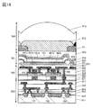
- FIG. 14 is a cross-sectional view illustrating the pixels.
- FIG. 15 is a cross-sectional view illustrating the pixels.
- FIG. 16 is a cross-sectional view illustrating the pixels.
- 17A to 17D are diagrams for explaining an OS transistor.
- FIG. 18 is a cross-sectional view illustrating the pixels.
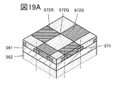
- 19A to 19C are perspective views (cross-sectional views) illustrating pixels.
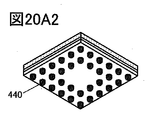
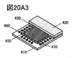
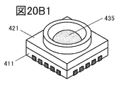
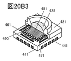
- 20A1 to 20A3 and 20B1 to 20B3 are perspective views of a package and a module containing an imaging device.
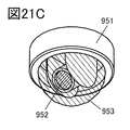
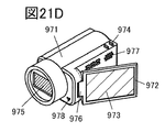
- 21A to 21F are diagrams for explaining electronic devices.
- FIG. 22 is a diagram illustrating an automobile.
- the element may be composed of a plurality of elements as long as there is no functional inconvenience.
- a plurality of transistors operating as switches may be connected in series or in parallel.
- the capacitor may be divided and arranged at a plurality of positions.
- one conductor may have a plurality of functions such as wiring, electrodes, and terminals, and in the present specification, a plurality of names may be used for the same element. Further, even if the elements are shown to be directly connected on the circuit diagram, the elements may actually be connected via one or a plurality of conductors. , In the present specification, such a configuration is also included in the category of direct connection.
- the imaging device holds analog data (image data) acquired in the imaging operation in pixels, and can extract data obtained by multiplying the analog data by an arbitrary weighting coefficient.
- the difference data between the adjacent light receiving devices can be acquired, and the information of the luminance gradient can be obtained.
- the information By incorporating the information into a neural network or the like, it is possible to infer distance information or the like. Further, since a huge amount of image data can be held in the pixels in the state of analog data, processing can be performed efficiently.
- the distance information in the image it is possible to support the picking work by the robot, the automatic driving of the moving body, the distance measurement, and the like. Further, in smartphones and the like, a plurality of cameras are used to acquire distance information, but distance information can be obtained with one camera, and the manufacturing cost can be reduced.
- FIG. 1 is a block diagram illustrating an imaging device according to an aspect of the present invention.
- the imaging device includes a pixel array 300, a circuit 301, a circuit 302, a circuit 303, a circuit 304, and a circuit 305.
- Each of the circuits 301 to 305 is not limited to a single circuit configuration, and may be configured by a combination of a plurality of circuits. Alternatively, any one of the above circuits may be integrated. Further, a circuit other than the above may be connected.
- the pixel array 300 has an imaging function and a calculation function.
- the circuit 301 has an arithmetic function.
- the circuit 302 has an arithmetic function or a data conversion function.
- the circuits 303 and 304 have a selection function.
- the circuit 305 has a function of supplying a potential for multiply-accumulate calculation to the pixels.
- a shift register, a decoder, or the like can be used for the circuit having the selection function.
- the circuits 301 and 302 may be provided externally.
- the pixel array 300 has a plurality of pixel blocks 200. As shown in FIG. 2, the pixel block 200 has a pixel array 210 and a circuit 220.
- the pixel array 210 has a plurality of pixels 100 arranged in a matrix, and each pixel 100 is electrically connected to the wiring 151 and the wiring 152, and the wiring 151 and the wiring 152 are electrically connected to the circuit 220, respectively. Connected to.
- the circuit 220 is a read circuit and has a circuit 230 and a circuit 240.
- the circuit 230 is a current source circuit and has a function of controlling the current flowing through the pixel array 210 and the circuit 240.
- the circuit 240 is a difference extraction circuit, and for example, a correlated double sampling circuit (CDS circuit) can be used.
- CDS circuit correlated double sampling circuit
- the circuit 230, the circuit 240, and the pixel array 210 are preferably formed so that any two or more of them have an overlapping region. With this configuration, the area of the pixel block 200 can be reduced and the resolution can be increased.
- the circuit 240 can also be provided outside the pixel block 200.
- the number of pixels of the pixel array 210 is set to 3 ⁇ 3 as an example, but the number of pixels is not limited to this. For example, it can be 2 ⁇ 2, 4 ⁇ 4, or the like. Alternatively, the number of pixels in the horizontal direction and the number of pixels in the vertical direction may be different. Alternatively, a switch or the like may be provided between the pixel 100 and the wiring 151 and the wiring 152 to make the number of pixels variable. Further, some pixels may be shared by adjacent pixel blocks 200. Further, an amplifier circuit or a gain adjustment circuit may be electrically connected to the wiring 151.
- the pixel 100 can acquire image data, generate arithmetic data using the image data, generate data obtained by adding the arithmetic data and a weighting coefficient, and the like. Further, the pixel block 200 having the above configuration can be operated as a product-sum calculation circuit.
- FIG. 10 A configuration example of the pixel 100 is shown in FIG.
- the pixel 100 has circuits 10a and 10b, a circuit 20, and a circuit 30.
- the circuits 10a and 10b are light receiving circuits and have a function of generating imaging data by a photoelectric conversion device.
- the circuit 20 is a differential amplifier circuit, and has a function of outputting an amplified data potential according to a difference in data input from the circuit 10a and the circuit 10b.
- the circuit 30 is an arithmetic circuit, and has a function of holding a data potential output from the circuit 20 and a function of giving a weight (potential corresponding to a weighting coefficient) to the data potential.
- the circuits 10a and 10b can have the same configuration, and include a photoelectric conversion device 101 (photoelectric conversion devices 101a and 101b), transistors 102 (transistors 102a and 102b), transistors 103 (transistors 103a and 103b), and a capacitor 106. (Capacitors 106a, 106b) can be provided.
- One electrode of the photoelectric conversion device 101 is electrically connected to one of the source and drain of the transistor 102.
- the other of the source or drain of the transistor 102 is electrically connected to one of the source or drain of the transistor 103 and one of the electrodes of the capacitor 106.
- the other electrode of the photoelectric conversion device 101 is electrically connected to the wiring 114.
- the other of the source or drain of the transistor 103 is electrically connected to the wiring 115.
- the gate of the transistor 102 is electrically connected to the wiring 116.
- the gate of the transistor 103 is electrically connected to the wiring 117.
- a node FD (node FDa, node FDb) is an electrical connection point between the other of the source or drain of the transistor 102, one of the source or drain of the transistor 103, and one electrode of the capacitor 106.
- the wirings 114 and 115 can have a function as a power supply line.
- the wiring 114 can function as a high-potential power supply line
- the wiring 115 can function as a low-potential power supply line.
- the wirings 116 and 117 can function as signal lines for controlling the continuity of each transistor.
- a photodiode can be used as the photoelectric conversion device 101. Regardless of the type of photodiode, a Si photodiode having silicon in the photoelectric conversion layer, an organic photodiode having an organic photoconductive film in the photoelectric conversion layer, or the like can be used. If it is desired to increase the light detection sensitivity at low illuminance, it is preferable to use an avalanche photodiode.
- the transistor 102 can have a function of controlling the potential of the node FD.
- the transistor 103 can have a function of initializing the potential of the node FD.
- a high voltage may be applied, and it is preferable to use a high voltage transistor for the transistor connected to the photoelectric conversion device 101.
- a high voltage transistor for example, a transistor using a metal oxide in the channel forming region (hereinafter, OS transistor) or the like can be used. Specifically, it is preferable to apply an OS transistor to the transistor 102.
- the OS transistor also has a characteristic that the off-current is extremely low.
- the period during which the electric charge can be held in the node FD can be extremely extended. Therefore, it is possible to apply the global shutter method in which charge accumulation operation is performed simultaneously in all pixels without complicating the circuit configuration and operation method. Further, while holding the image data in the node FD, it is possible to perform a plurality of operations using the image data.
- Si transistor silicon in the channel forming region
- an OS transistor and a Si transistor may be arbitrarily combined and applied.
- the Si transistor include a transistor having amorphous silicon, a transistor having crystalline silicon (microcrystalline silicon, low temperature polysilicon, single crystal silicon), and the like.
- the above is an example of the circuit configuration of the circuits 10a and 10b, and the photoelectric conversion operation can be performed by another circuit configuration.
- the circuits 10a and 10b may have a configuration including transistors 175 (transistors 175a and 175b) and transistors 176 (transistors 176a and 176b).
- the gate of transistor 175 is electrically connected to the node FD.
- One of the source or drain of the transistor 175 is electrically connected to the wiring 118, and the other of the source or drain of the transistor 175 is electrically connected to one of the source or drain of the transistor 176.
- the other of the source or drain of the transistor 176 is electrically connected to the wiring OUT.
- the wiring 118 can function as a power supply line and may be connected to the wiring 115.
- the transistor 175 is a source follower element that outputs data according to the potential of the node FD. Further, the transistor 176 functions as a selection transistor for selecting a light receiving circuit to be read. Therefore, by using the circuits 10a and 10b having the configuration of FIG. 4A, the image data can be read out from each light receiving circuit to the wiring OUT. Further, in this configuration, image data can be read out in parallel with the operation of the circuit 20.
- the circuit 20 can include a transistor 104 (transistors 104a, 104b), a transistor 105 (transistors 105a, 105b), a transistor 107, a transistor 108, and a transistor 131 (transistors 131a, 131b).
- One of the source or drain of transistor 104a is electrically connected to one of the gate of transistor 105a and one of the source or drain of transistor 107.
- One of the source or drain of transistor 104b is electrically connected to the gate of transistor 105b and the other of source or drain of transistor 107.
- One of the source or drain of the transistor 105a is electrically connected to one of the source or drain of the transistor 131a and the gate.
- One of the source or drain of transistor 105b is electrically connected to one of the source or drain of transistor 131b and the gate.
- the other of the source or drain of the transistor 105a is electrically connected to the other of the source or drain of the transistor 105b and one of the source or drain of the transistor 108.
- the other of the source or drain of the transistor 131 is electrically connected to the wiring 124.
- the other of the source or drain of the transistor 108 is electrically connected to a reference potential line or a low potential power supply line such as GND wiring.
- the gate of the transistor 104a is electrically connected to the wiring 121.
- the gate of the transistor 104b is electrically connected to the wiring 122.
- the gate of the transistor 107 is electrically connected to the wiring 123.
- the wiring 124 can have a function as, for example, a power supply line for supplying a high potential power source.
- the wiring 121, the wiring 122, and the wiring 123 can have a function as a signal line for controlling the continuity of each transistor.
- the transistor 104 functions as a switch.
- the other of the source or drain of the transistor 104a is electrically connected to the node FDa of the circuit 10a.
- the other side of the source or drain of the transistor 104b is electrically connected to the node FDb of the circuit 10b. Therefore, it can be said that the transistor 104 is an element of the circuits 10a and 10b.
- the transistor 105 functions as a differential transistor pair in the differential amplifier circuit.
- the gate of the transistor 105a functions as a first input terminal of the circuit 20.
- the gate of the transistor 105b functions as a second input terminal of the circuit 20. Therefore, the data generated by the circuit 10a can be input to the first input terminal. Further, the data generated by the circuit 10b can be input to the second input terminal.
- the transistor 107 functions as a switch, and the first input terminal and the second input terminal can have the same potential.
- the switch can be used when acquiring reference data.
- the transistor 108 functions as a current source, and an appropriate potential (Bias) is supplied to the gate.
- An appropriate potential (Bias) is supplied to the gate.
- a resistance element may be used instead of the transistor 108.
- the transistor 131 functions as a voltage conversion circuit. Although the transistor 131 is illustrated as a diode-connected p-channel transistor in FIG. 3, it may be a diode-connected n-channel transistor. Alternatively, a diode element, a resistance element, or a cascode circuit may be used instead of the transistor 131.
- a part of the wiring connecting one of the source or drain of the transistor 105b and one of the source or drain of the transistor 131b also functions as an output terminal, and is represented as a node N in FIG.
- An amplified data potential can be output to the output terminal (node N) according to the difference between the output data of the circuit 10a and the output data of the circuit 10b.
- the circuit 20 may have a configuration in which the transistor 104 and the transistor 107 are omitted.
- the transistor 104 and the transistor 107 are provided so that the first input terminal and the second input terminal have the same potential, but if the potential (reset potential) of the wiring 115 supplied from the transistor 103 is used as the potential, the potential of the wiring 115 (reset potential) can be used.
- the transistor 104 and the transistor 107 can be omitted.
- the circuit 30 can have a configuration including a transistor 132, a transistor 133, a transistor 134, a transistor 142, a transistor 143, a transistor 144, a capacitor 135, and a capacitor 145.
- One of the source or drain of transistor 132 is electrically connected to one electrode of capacitor 135 and the gate of transistor 133.
- the other electrode of the capacitor 135 is electrically connected to one of the source or drain of the transistor 134.
- One of the source or drain of the transistor 142 is electrically connected to one electrode of the capacitor 145 and the gate of the transistor 143.
- the other electrode of the capacitor 145 is electrically connected to one of the source or drain of the transistor 144.
- the gate of the transistor 132 is electrically connected to the wiring 125.
- the gate of the transistor 142 is electrically connected to the wiring 126.
- the gate of the transistor 134 and the gate of the transistor 144 are electrically connected to the wiring 127.
- the other source or drain of transistor 132 and the other source or drain of transistor 142 are electrically connected to node N.
- the other of the source or drain of the transistor 134 and the other of the source or drain of the transistor 144 are electrically connected to the wiring 128.
- One of the source and drain of the transistor 133 is electrically connected to the wiring 151.
- One of the source or drain of the transistor 143 is electrically connected to the wiring 152.
- the other of the source or drain of the transistor 133 and the other of the source or drain of the transistor 143 are electrically connected to a reference or low potential line of force such as GND wiring.
- the wiring 125, the wiring 126, and the wiring 127 can have a function as a signal line for controlling the continuity of each transistor.
- the wiring 128 is, for example, a wiring capable of supplying a potential corresponding to a weighting coefficient (such as a filter for convolution processing), and is electrically connected to the circuit 305 (see FIG. 1).
- the wiring 151 is a wiring electrically connected to the circuit 230 and the circuit 240, and the wiring 152 is a wiring electrically connected to the circuit 230 (see FIG. 2).
- a point (wiring) to which one of the source or drain of the transistor 132, one electrode of the capacitor 135, and the gate of the transistor 133 are connected is referred to as a node P1.
- a point (wiring) to which one of the source or drain of the transistor 142, one electrode of the capacitor 145, and the gate of the transistor 143 is connected is referred to as a node P2.
- Data output by the circuit 20 can be stored in the node P1 and the node P2. Further, the node P1 and the node P2 can be made floating. Therefore, the potential (weighting coefficient) supplied from the wiring 128 can be given to the data held in the node P1 and the node P2 by the capacitive coupling of the capacitor 135 or the capacitor 145.
- the readout circuit 220 includes a circuit 230 that functions as a current source circuit and a circuit 240 that functions as a difference extraction circuit.
- the circuit 230 can flow a current according to the data held in the pixel 100, and can be configured as shown in FIG. 5A, for example.
- the circuit 230 can be configured to include a current supply unit 225 and a current mirror unit 226.
- FIG. 5A shows a configuration using an n-ch type transistor.
- the current supply unit 225 may have a configuration including transistors 222 and 252 and transistors 223 and 253.
- One of the source and drain of the transistor 222 is electrically connected to the signal line FG.
- the other of the source or drain of transistor 222 is electrically connected to the gate of transistor 223.
- One of the source and drain of the transistor 252 is electrically connected to the signal line FGREF.
- the other of the source or drain of transistor 252 is electrically connected to the gate of transistor 253.
- the gate of transistor 222 and the gate of transistor 252 are electrically connected to wiring 213.
- One of the source or drain of the transistor 223 is electrically connected to the wiring 151.
- One of the source or drain of the transistor 253 is electrically connected to the wiring 152.
- the other of the source or drain of the transistor 223 and the other of the source or drain of the transistor 253 are electrically connected to the high potential power line (VDD).
- an appropriate signal potential is supplied to the signal lines FG and FGREF, and by supplying a high potential (“H”) to the wiring 213, the transistors 222 and 252 and the transistors 223 and 253 become conductive.
- the wiring 151 and the wiring 152 can be supplied with an electric current.
- the current mirror unit 226 may have a transistor 254 and a transistor 224.
- One of the gate and source or drain of transistor 254 is electrically connected to wire 152.
- One of the source or drain of the transistor 224 is electrically connected to the wiring 151.
- the other source or drain of transistor 224 and the other source or drain of transistor 254 are electrically connected to a low potential power line (VSS).
- the gate of the transistor 224 is electrically connected to the gate of the transistor 254, and the same current (ICM) as that of the transistor 254 can be passed through the transistor 224.
- the current supply unit 225 may have a configuration using a p-ch type transistor as shown in FIG. 5B.
- the output side of the transistor 262 is electrically connected to the wiring 152 and the gate of the transistor 261.
- the circuit 240 is a difference extraction circuit, and the product of the data and the weighting coefficient (product-sum calculation result) can be extracted by using the current flowing through the pixel 100 and the circuit 230. As shown in FIG. 2, each pixel 100 is electrically connected to each other by wiring 151. The circuit 240 can perform calculations using the sum of the currents flowing through the transistors 133 of each pixel 100.
- the circuit 240 includes a capacitor 202, a transistor 203, a transistor 204, a transistor 205, a transistor 206, and a transistor 207 as a voltage conversion circuit.
- An appropriate analog potential (Bias) is applied to the gate of transistor 207.
- One electrode of the capacitor 202 is electrically connected to one of the source or drain of transistor 203 and the gate of transistor 204.
- One of the source or drain of transistor 204 is electrically connected to one of the source or drain of transistor 205 and one of the source or drain of transistor 206.
- the other electrode of the capacitor 202 is electrically connected to one of the wires 151 and the source or drain of the transistor 207.
- a point connecting one electrode of the capacitor 202, one of the source or drain of the transistor 203, and the gate of the transistor 204 is referred to as a node C.
- the other of the source or drain of transistor 203 is electrically connected to wiring 218.
- the other of the source or drain of transistor 204 is electrically connected to wire 219.
- the other of the source or drain of the transistor 205 is electrically connected to a reference power line such as GND wiring.
- the other of the source or drain of the transistor 206 is electrically connected to the wiring 212.
- the other of the source or drain of transistor 207 is electrically connected to a reference power line such as GND wiring.
- the gate of transistor 203 is electrically connected to wiring 216.
- the gate of the transistor 205 is electrically connected to the wiring 215.
- the gate of transistor 206 is electrically connected to wiring 214.
- Wiring 218 and 219 can have a function as a power supply line.
- the wiring 218 can have a function as a wiring for supplying a reset potential (Vr) for reading.
- the wiring 219 can function as a high-potential power supply line.
- the wirings 214, 215, and 216 can function as signal lines for controlling the continuity of each transistor.
- the wiring 212 is an output line and can be electrically connected to, for example, the circuit 301 shown in FIG.
- the transistor 203 can have a function of resetting the potential of the node C to the potential of the wiring 218.
- the transistors 204 and 205 can have a function as a source follower circuit.
- the transistor 206 can have a function of controlling reading.
- the circuit 240 has a function as a correlated double sampling circuit (CDS circuit), and can be replaced with a circuit having another configuration having the function.
- CDS circuit correlated double sampling circuit
- the data obtained by voltage-converting the current flowing from the circuit 230 to the circuit 240 based on the reference data and the difference data and the current flowing from the circuit 230 to the circuit 240 when the reference data and the difference data are weighted are voltage-converted.
- the differential potential with the data is extracted by the circuit 240.
- the differential potential corresponds to data obtained by removing various offset components from the current flowing through the circuit 220, and is data obtained by voltage-converting the current represented by the term of the product of the difference data and the weighting coefficient. That is, the product of the difference data and the weighting coefficient can be extracted.
- the description of the operation of the pixel 100 is omitted, and the difference data (obtained by photoelectric conversion) of the circuit 10a and the circuit 10b is connected to the node P1.
- the data potential X corresponding to the difference between the data) is stored, and the data potential (reference data, ideally 0) output by the circuit 20 when there is no difference between the outputs of the circuit 10a and the circuit 10b is stored in the node P2. It will be described as being in the stored state. The detailed operation of the pixel 100 will be described later.
- an offset component other than the product of the difference data (potential X) and the weighting coefficient (potential W) can be removed to extract the target WX.
- the flow of WX extraction when the circuit shown in FIG. 5A is used as the circuit 230 is as follows.
- the transistor 203 is brought into a conductive state, and the potential Vr is written from the wiring 218 to the node C.
- the potential Vr is a reset potential used for the read operation.
- the difference data (potential X) is written in the node P1 of the circuit 30 of the pixel 100. Further, it is assumed that the reference data 0 is written in the node P2. Further, the weighting coefficient written from the wiring 128 is set to 0.
- the total current flowing from the circuit 230 to the transistor 133 of each pixel 100 is k ⁇ (XV th ) 2 . Further, the total current flowing from the circuit 230 to the transistor 143 of each pixel 100 is k ⁇ (0 ⁇ V th ) 2 .
- k is a constant and Vth is the threshold voltage of each transistor.
- the total current flowing through the transistor 223 is defined as an IC
- the total current flowing through the transistor 253 is defined as an ICFEF
- the total current flowing through the transistor 224 and the transistor 254 is defined as an ICM (see FIG. 5A).
- ICM 0 ICREF 0- k ⁇ (0-V th ) 2 .
- the transistor 203 of the circuit 240 is brought into a non-conducting state, and the potential Vr is held at the node C.
- a potential corresponding to the weighting coefficient (W) is supplied to the wiring 128, and the weighting coefficient (W) is given to the node P1 and the node P2 by capacitive coupling.
- the total current flowing from the circuit 230 to the transistor 133 of each pixel 100 is k ⁇ (X + W ⁇ V th ) 2 . Further, the total current flowing from the circuit 230 to the transistor 143 of each pixel 100 is k ⁇ (WV th ) 2 .
- the difference can be extracted by the circuit 240.
- IR 0 is initialized as the potential Vr of the node C, and the potential of the wiring 151 changes from the state of the weight coefficient 0 to the state of the weight coefficient W when the node C is floating. ( Corresponding to the difference between IR 0 and IR) is added to the node C by the capacitive coupling of the capacitor 202.
- the pixel 100 described here has the configuration shown in FIG. Further, it is assumed that a predetermined potential is supplied to the power supply line and the like.
- the transistor 104b and the transistor 107 are conductive, and the potential of the node FDb is input to the first input terminal (gate of the transistor 105a) and the second input terminal (gate of the transistor 105b) of the circuit 20.
- the output terminal (node N) of the circuit 20 outputs the amplified data potential according to the difference between the data input to the first input terminal and the data input to the second input terminal. ..
- the data potential output to the output terminal (node N) of the circuit 20 can be referred to as reference data.
- the reference data is data that is output when there is no difference between the data input to the first input terminal and the data input to the second input terminal.
- the reference data may be output when the node FDa and the node FDb are set to the reset potentials.
- the potential of the wiring 126 is "H" at time T4
- the potential of the output terminal (node N) of the circuit 20 is written to the node P2 of the circuit 30.
- the potential of the wiring 126 is set to “L”, and the potential of the node P2 is held.
- the potential of the wiring 127 is set to "H”
- the potential of the other electrode of the capacitors 135 and 145 is set to the potential of the wiring 128 (for example, 0).
- the data potential amplified according to the difference between the node FDa and the node FDb is output to the output terminal (node N) of the circuit 20.
- the data potential output to the output terminal (node N) of the circuit 20 is a potential amplified according to the difference between the image data acquired by the circuit 10a and the image data acquired by the circuit 10b, and is different from the difference data. Can be called. Alternatively, it can also be called image data or imaging data.
- the potential of the wiring 125 is "H” at time T6
- the potential of the output terminal (node N) of the circuit 20 is written to the node P1 of the circuit 30.
- the potential of the wiring 125 is set to “L”, and the potential of the node P1 is held.
- the ICREF is the sum of the current (ICM) flowing through the transistor 254 and the current flowing through the transistor 143 of the circuit 30.
- the current IC is the sum of the current (ICM) flowing through the transistor 224, the current flowing through the transistor 133 of the circuit 30, and the current flowing through the transistor 207 of the circuit 240.
- the potential of the wiring 151 is determined in the above state, the potential of the wiring 216 is set to "H”, and the potential “Vr" of the wiring 218 is written to the node C. Then, the potential of the wiring 216 is set to "L”, the node C is set to floating, and the potential "Vr" is held.
- the circuit 240 can output the signal potential corresponding to the WX to the wiring 212 by the source follower operation.
- the potential of the wiring 127 is set to "L”
- the potential of the wiring 213 is set to “L”
- the potential of the wiring 214 is set to “L”
- the potential of the wiring 215 is set to “L”
- the WX output from the circuit 240 by the above operation can be input to the circuit 301.
- the data of the node P1 and the node P2 may have a time difference.
- information including motion parallax can be extracted.
- Depth (distance) information can be obtained from motion parallax, and a stereoscopic image can be constructed.
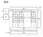
- FIG. 7A is a diagram illustrating a circuit 301 and a circuit 302 connected to the circuit 240.
- the product-sum calculation result data output from the circuit 240 is sequentially input to the circuit 301.
- the circuit 301 may have various arithmetic functions. Alternatively, the function of the circuit 301 may be replaced by software processing.
- the circuit 301 can have a circuit that performs an operation of an activation function.
- a comparator circuit can be used for the circuit.
- the comparator circuit outputs the result of comparing the input data with the set threshold value as binary data. That is, the pixel block 200 and the circuit 301 can act as a part of the neural network.
- the circuit 301 may have an A / D converter.
- the circuit 301 can convert the analog data into digital data.
- the circuit 10a and the circuit 10b shown in FIG. 4A can be electrically connected to the circuit 301 via the wiring OUT.
- the data output by the pixel block 200 corresponds to the image data of a plurality of bits, but if it can be binarized by the circuit 301, it can be said that the image data is compressed.
- the data output from the circuit 301 is sequentially input to the circuit 302.
- the circuit 302 can be configured to include, for example, a latch circuit and a shift register. With this configuration, parallel serial conversion can be performed, and the data input in parallel can be output to the wiring 311 as serial data.
- the connection destination of the wiring 311 is not limited. For example, it can be connected to a neural network, a storage device, a communication device, or the like.
- the circuit 302 may have a neural network.
- the neural network has memory cells arranged in a matrix, and each memory cell holds a weighting coefficient.
- the data output from the circuit 301 is input to each of the memory cells 320, and the product-sum operation can be performed.
- the number of memory cells shown in FIG. 7B is an example and is not limited.
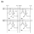
- the neural network shown in FIG. 7B has memory cells 320 and reference memory cells 325 installed in a matrix, a circuit 330, a circuit 350, a circuit 360, and a circuit 370.
- FIG. 8 shows an example of the memory cell 320 and the reference memory cell 325.
- Reference memory cells 325 are provided in an arbitrary row.
- the memory cell 320 and the reference memory cell 325 have a similar configuration and include a transistor 161 and a transistor 162 and a capacitor 163.
- One of the source or drain of transistor 161 is electrically connected to the gate of transistor 162.
- the gate of transistor 162 is electrically connected to one electrode of capacitor 163.
- a node NM is a point where one of the source and drain of the transistor 161, the gate of the transistor 162, and one electrode of the capacitor 163 are connected.
- the gate of the transistor 161 is electrically connected to the wiring WL.
- the other electrode of the capacitor 163 is electrically connected to the wiring RW.
- One of the source and drain of the transistor 162 is electrically connected to a reference potential wiring such as a GND wiring.
- the other of the source or drain of the transistor 161 is electrically connected to the wiring WD.
- the other of the source or drain of the transistor 162 is electrically connected to the wiring BL.
- the other of the source or drain of the transistor 161 is electrically connected to the wiring WDref.
- the other of the source or drain of the transistor 162 is electrically connected to the wiring BLref.
- the wiring WL is electrically connected to the circuit 330.
- a decoder, a shift register, or the like can be used for the circuit 330.
- the wiring RW is electrically connected to the circuit 301.
- Binary data output from the circuit 301 is written to each memory cell.
- a sequential circuit such as a shift register may be provided between the circuit 301 and each memory cell.
- the wiring WD and the wiring WDref are electrically connected to the circuit 350.
- a decoder, a shift register, or the like can be used for the circuit 350.
- the circuit 350 may have a D / A converter and an SRAM.
- the circuit 350 can output the weighting factor written to the node NM.
- the wiring BL and the wiring BLref are electrically connected to the circuit 360.
- the circuit 360 can have the same configuration as the circuit 240.
- the circuit 360 can obtain a signal obtained by removing the offset component from the product-sum calculation result.
- the circuit 360 is electrically connected to the circuit 370.
- the circuit 370 can also be rephrased as an activation function circuit.
- the activation function circuit has a function of performing an operation for converting a signal input from the circuit 360 according to a predefined activation function.
- As the activation function for example, a sigmoid function, a tanh function, a softmax function, a ReLU function, a threshold function, and the like can be used.
- the signal converted by the activation function circuit is output to the outside as output data.
- the neural network NN can be composed of an input layer IL, an output layer OL, and an intermediate layer (hidden layer) HL.
- the input layer IL, the output layer OL, and the intermediate layer HL each have one or more neurons (units).
- the intermediate layer HL may be one layer or two or more layers.
- a neural network having two or more intermediate layers HL can also be called a DNN (deep neural network). Learning using a deep neural network can also be called deep learning.
- Input data is input to each neuron in the input layer IL.
- the output signals of the neurons in the anterior layer or the posterior layer are input to each neuron in the middle layer HL.
- the output signals of the neurons in the presheaf layer are input to each neuron in the output layer OL.
- Each neuron may be connected to all neurons in the anterior and posterior layers (fully connected), or may be connected to some neurons.
- FIG. 9B shows an example of calculation by neurons.
- two neurons in the presheaf layer that output a signal to the neuron N and the neuron N are shown.
- the output x 1 of the presheaf neuron and the output x 2 of the presheaf neuron are input to the neuron N.
- the sum of the multiplication result of the output x 1 and the weight w 1 (x 1 w 1 ) and the multiplication result of the output x 2 and the weight w 2 (x 2 w 2 ) is x 1 w 1 + x 2 w 2.
- the operation by the neuron includes the operation of adding the product of the output of the neuron in the previous layer and the weight, that is, the product-sum operation (x 1 w 1 + x 2 w 2 above ).
- This product-sum operation may be performed by software using a program or by hardware.
- the product-sum calculation is performed using an analog circuit as hardware.
- an analog circuit is used for the product-sum calculation circuit, the processing speed can be improved and the power consumption can be reduced by reducing the circuit scale of the product-sum calculation circuit or reducing the number of times the memory is accessed.
- the product-sum calculation circuit preferably has an OS transistor. Since the OS transistor has an extremely small off current, it is suitable as a transistor constituting an analog memory of a product-sum calculation circuit.
- the product-sum calculation circuit may be configured by using both the Si transistor and the OS transistor.
- FIG. 10A is a diagram showing an example of the pixel structure of the image pickup apparatus, and can be a laminated structure of layers 561 and 563.
- Layer 561 has a photoelectric conversion device 101.
- the photoelectric conversion device 101 can have a layer 565a and a layer 565b as shown in FIG. 11A. In some cases, the layer may be referred to as an area.
- the photoelectric conversion device 101 shown in FIG. 11A is a pn junction type photodiode.
- a p-type semiconductor can be used for the layer 565a and an n-type semiconductor can be used for the layer 565b.
- an n-type semiconductor may be used for the layer 565a and a p-type semiconductor may be used for the layer 565b.
- the pn junction type photodiode can be typically formed by using single crystal silicon.
- a photodiode having a single crystal silicon as a photoelectric conversion layer has a relatively wide spectral sensitivity characteristic from ultraviolet light to near infrared light, and can detect light of various wavelengths by combining with an optical conversion layer described later. Can be done.
- a compound semiconductor may be used as the photoelectric conversion layer of the pn junction type photodiode.
- the compound semiconductor include gallium-arsenide-phosphorus compound (GaAsP), gallium-phosphorus compound (GaP), indium-gallium-arsenide compound (InGaAs), lead-sulfur compound (PbS), and lead-selenium compound (PbSe). ), Indium-arsenide compound (InAs), indium-antimonide compound (InSb), mercury-cadmium-tellulu compound (HgCdTe) and the like can be used.
- the compound semiconductor includes a compound semiconductor having Group 13 elements (aluminum, gallium, indium, etc.) and Group 15 elements (nitrogen, phosphorus, arsenic, antimony, etc.) (also referred to as Group 3-5 compound semiconductor), or Group 12 elements. It is preferably a compound semiconductor (also referred to as a Group 2-6 compound semiconductor) having (magnesium, zinc, cadmium, mercury, etc.) and Group 16 elements (oxygen, sulfur, selenium, tellurium, etc.).
- the band gap of a compound semiconductor can be changed according to the combination of constituent elements and the atomic number ratio thereof, a photodiode having sensitivity in various wavelength ranges from ultraviolet light to infrared light can be formed.
- the wavelength of ultraviolet light is around 0.01 ⁇ m to 0.38 ⁇ m
- the wavelength of visible light is around 0.38 ⁇ m to 0.75 ⁇ m
- the wavelength of near infrared light is around 0.75 ⁇ m to 2.5 ⁇ m.
- the wavelength of mid-infrared light can be generally defined as around 2.5 ⁇ m to 4 ⁇ m
- the wavelength of far-infrared light can be generally defined as near 4 ⁇ m to around 1000 ⁇ m.
- GaP gallium phosphide
- the photoelectric conversion layer in order to form a photodiode having light sensitivity from ultraviolet light to visible light, GaP or the like can be used for the photoelectric conversion layer.
- the above-mentioned silicon or GaAsP can be used for the photoelectric conversion layer.
- InGaAs or the like in order to form a photodiode having light sensitivity from visible light to mid-infrared light.
- PbS, InAs, or the like can be used for the photoelectric conversion layer.
- PbSe, InSb, HgCdTe or the like can be used for the photoelectric conversion layer.
- the photodiode using the compound semiconductor may be a pin junction as well as a pn junction. Further, the pn junction and the pin junction are not limited to the homozygous structure, and may be a heterojunction structure.
- a first compound semiconductor can be used for one layer of the pn junction structure, and a second compound semiconductor different from the first compound semiconductor can be used for the other layer.
- a first compound semiconductor can be used for any one or two layers of the pin junction structure, and a second compound semiconductor different from the first compound semiconductor can be used for the other layers.
- One of the first compound semiconductor and the second compound semiconductor may be a single semiconductor such as silicon.
- the photoelectric conversion layer of the photodiode may be formed by using a different material for each pixel. Pixels that detect ultraviolet light by using this configuration. It is possible to form an image pickup apparatus having any two types of pixels, such as a pixel that detects visible light and a pixel that detects infrared light, or three types of pixels.
- the photoelectric conversion device 101 included in the layer 561 may be a laminate of the layer 566a, the layer 566b, the layer 566c, and the layer 566d.
- the photoelectric conversion device 101 shown in FIG. 11B is an example of an avalanche photodiode, in which layers 566a and 566d correspond to electrodes, and layers 566b and 566c correspond to photoelectric conversion units.
- the layer 566a is preferably a low resistance metal layer or the like.
- a low resistance metal layer or the like aluminum, titanium, tungsten, tantalum, silver or a laminate thereof can be used.
- the layer 566d it is preferable to use a conductive layer having high translucency with respect to visible light.
- a conductive layer having high translucency with respect to visible light For example, indium oxide, tin oxide, zinc oxide, indium-tin oxide, gallium-zinc oxide, indium-gallium-zinc oxide, graphene and the like can be used.
- the layer 566d may be omitted.
- the layers 566b and 566c of the photoelectric conversion unit can be configured as a pn junction type photodiode using, for example, a selenium-based material as a photoelectric conversion layer. It is preferable that a selenium-based material, which is a p-type semiconductor, is used as the layer 566b, and gallium oxide, which is an n-type semiconductor, is used as the layer 566c.
- a photoelectric conversion device using a selenium-based material has a characteristic of high external quantum efficiency with respect to visible light.
- the amplification of electrons with respect to the amount of incident light can be increased by utilizing the avalanche multiplication.
- the selenium-based material has a high light absorption coefficient, it has a production advantage such that the photoelectric conversion layer can be formed of a thin film.
- a thin film of a selenium-based material can be formed by a vacuum vapor deposition method, a sputtering method, or the like.
- selenium-based material crystalline selenium (single crystal selenium, polycrystalline selenium) and amorphous selenium can be used. These have photosensitivity from ultraviolet light to visible light. Further, a compound of copper, indium and selenium (CIS), a compound of copper, indium, gallium and selenium (CIGS) and the like can be used. These have photosensitivity from ultraviolet light to near infrared light.
- CIS copper, indium and selenium
- CGS indium, gallium and selenium
- the n-type semiconductor is preferably formed of a material having a wide bandgap and translucency with respect to visible light.
- a material having a wide bandgap and translucency with respect to visible light For example, zinc oxide, gallium oxide, indium oxide, tin oxide, or an oxide in which they are mixed can be used.
- these materials also have a function as a hole injection blocking layer, and can reduce the dark current.
- the photoelectric conversion device 101 included in the layer 561 may be a laminate of the layer 567a, the layer 567b, the layer 567c, the layer 567d, and the layer 567e.
- the photoelectric conversion device 101 shown in FIG. 11C is an example of an organic photoconductive film, layer 567a is a lower electrode, layer 567e is a translucent upper electrode, and layers 567b, 567c, and 567d correspond to a photoelectric conversion unit. ..
- One of the layers 567b and 567d of the photoelectric conversion unit can be a hole transport layer and the other can be an electron transport layer. Further, the layer 567c can be a photoelectric conversion layer.
- the hole transport layer for example, molybdenum oxide or the like can be used.
- the electron transport layer for example, fullerenes such as C 60 and C 70 , or derivatives thereof and the like can be used.
- the photoelectric conversion layer a mixed layer (bulk heterojunction structure) of an n-type organic semiconductor and a p-type organic semiconductor can be used.
- a mixed layer bulk heterojunction structure
- organic semiconductors There are various types of organic semiconductors, and a material having photosensitivity at a target wavelength may be selected for the photoelectric conversion layer.
- a silicon substrate can be used as the layer 563 shown in FIG. 10A.
- the silicon substrate has a Si transistor and the like.
- the Si transistor can be used to form a circuit for driving the pixel circuit, an image signal readout circuit, an image processing circuit, a neural network, a communication circuit, and the like.
- a storage circuit such as a DRAM (Dynamic Random Access Memory), a CPU (Central Processing Unit), an MCU (Micro Controller Unit), or the like may be formed.
- the above circuit excluding the pixel circuit is referred to as a functional circuit.
- a part or all of them may be provided on the layer 563. can.
- the layer 563 may be a stack of a plurality of layers as shown in FIG. 10B.
- FIG. 10B three layers of layers 563a, 563b, and 563c are illustrated, but two layers may be used.
- the layer 563 may be a stack of four or more layers. These layers can be laminated by using, for example, a bonding step. With this configuration, the pixel circuit and the functional circuit can be dispersed in a plurality of layers, and the pixel circuit and the functional circuit can be provided in an overlapping manner, so that a compact and highly functional imaging device can be manufactured.
- the pixel may have a laminated structure of layers 561, 562, and 563.
- Layer 562 can have an OS transistor.
- One or more of the above-mentioned functional circuits may be formed of OS transistors.
- one or more functional circuits may be formed by using the Si transistor included in the layer 563 and the OS transistor included in the layer 562.
- the layer 563 may be used as a support substrate such as a glass substrate, and the functional circuit may be formed by the OS transistor included in the layer 562.
- a normally-off CPU (also referred to as "Noff-CPU") can be realized by using an OS transistor and a Si transistor.
- the Nonf-CPU is an integrated circuit including a normally-off type transistor that is in a non-conducting state (also referred to as an off state) even when the gate voltage is 0V.
- the Noff-CPU can stop the power supply to the unnecessary circuit in the Noff-CPU and put the circuit in the standby state. No power is consumed in the circuit where the power supply is stopped and the circuit is in the standby state. Therefore, the Nonf-CPU can minimize the amount of power used. Further, the Nonf-CPU can retain information necessary for operation such as setting conditions for a long period of time even if the power supply is stopped. To return from the standby state, it is only necessary to restart the power supply to the circuit, and it is not necessary to rewrite the setting conditions and the like. That is, high-speed recovery from the standby state is possible. In this way, the Nonf-CPU can reduce the power consumption without significantly reducing the operating speed.
- the layer 562 may be a stack of a plurality of layers as shown in FIG. 10D.
- FIG. 10D two layers of layers 562a and 563b are illustrated, but three or more layers may be laminated. These layers can be formed so as to be stacked on, for example, layer 563.
- the layer formed on the layer 563 and the layer formed on the layer 561 may be bonded together.
- a metal oxide having an energy gap of 2 eV or more, preferably 2.5 eV or more, more preferably 3 eV or more can be used.
- a typical example is an oxide semiconductor containing indium, and for example, CAAC-OS or CAC-OS, which will be described later, can be used.
- CAAC-OS is suitable for transistors and the like in which the atoms constituting the crystal are stable and reliability is important. Further, since CAC-OS exhibits high mobility characteristics, it is suitable for a transistor or the like that performs high-speed driving.
- the OS transistor Since the OS transistor has a large energy gap in the semiconductor layer, it exhibits an extremely low off-current characteristic of several yA / ⁇ m (current value per 1 ⁇ m of channel width). Further, the OS transistor has features different from those of the Si transistor such as impact ionization, avalanche breakdown, and short channel effect, and can form a circuit having high withstand voltage and high reliability. In addition, variations in electrical characteristics due to crystallinity non-uniformity, which is a problem with Si transistors, are unlikely to occur with OS transistors.
- the semiconductor layer of the OS transistor includes, for example, indium, zinc and M (one or more selected from metals such as indium, titanium, gallium, germanium, yttrium, zirconium, lanthanum, cerium, tin, neodymium or hafnium). It can be a film represented by an In—M—Zn-based oxide containing.
- the In—M—Zn-based oxide can be typically formed by a sputtering method. Alternatively, it may be formed by using an ALD (Atomic layer deposition) method.
- the atomic number ratio of the metal element of the sputtering target used for forming the In—M—Zn-based oxide by the sputtering method preferably satisfies In ⁇ M and Zn ⁇ M.
- the atomic number ratio of the semiconductor layer to be formed includes fluctuations of plus or minus 40% of the atomic number ratio of the metal element contained in the sputtering target.
- the semiconductor layer an oxide semiconductor having a low carrier density is used.
- the semiconductor layer has a carrier density of 1 ⁇ 10 17 / cm 3 or less, preferably 1 ⁇ 10 15 / cm 3 or less, more preferably 1 ⁇ 10 13 / cm 3 or less, and more preferably 1 ⁇ 10 11 / cm. 3 or less, more preferably less than 1 ⁇ 10 10 / cm 3, it is possible to use an oxide semiconductor of 1 ⁇ 10 -9 / cm 3 or more carrier density.
- Such oxide semiconductors are referred to as high-purity intrinsic or substantially high-purity intrinsic oxide semiconductors. It can be said that the oxide semiconductor is an oxide semiconductor having a low defect level density and stable characteristics.
- a transistor having an appropriate composition may be used according to the required semiconductor characteristics and electrical characteristics (field effect mobility, threshold voltage, etc.) of the transistor. Further, in order to obtain the required semiconductor characteristics of the transistor, it is preferable that the carrier density, impurity concentration, defect density, atomic number ratio of metal element and oxygen, interatomic distance, density and the like of the semiconductor layer are appropriate. ..
- the concentration of silicon or carbon in the semiconductor layer is set to 2 ⁇ 10 18 atoms / cm 3 or less, preferably 2 ⁇ 10 17 atoms / cm 3 or less.
- the concentration of alkali metal or alkaline earth metal in the semiconductor layer is 1 ⁇ 10 18 atoms / cm 3 or less, preferably 2 ⁇ 10 16 atoms / cm 3 or less.
- the nitrogen concentration in the semiconductor layer is preferably 5 ⁇ 10 18 atoms / cm 3 or less.
- the oxide semiconductor constituting the semiconductor layer when the oxide semiconductor constituting the semiconductor layer contains hydrogen, it reacts with oxygen bonded to a metal atom to become water, which may form an oxygen deficiency in the oxide semiconductor. If the channel formation region in the oxide semiconductor contains oxygen deficiency, the transistor may have a normally-on characteristic. In addition, a defect containing hydrogen in an oxygen deficiency may function as a donor and generate electrons as carriers. In addition, a part of hydrogen may be combined with oxygen that is bonded to a metal atom to generate an electron as a carrier. Therefore, a transistor using an oxide semiconductor containing a large amount of hydrogen tends to have a normally-on characteristic.
- Defects containing hydrogen in oxygen deficiencies can function as donors for oxide semiconductors. However, it is difficult to quantitatively evaluate the defect. Therefore, in oxide semiconductors, the carrier concentration may be evaluated instead of the donor concentration. Therefore, in the present specification and the like, as the parameter of the oxide semiconductor, the carrier concentration assuming a state in which an electric field is not applied may be used instead of the donor concentration. That is, the "carrier concentration" described in the present specification and the like may be paraphrased as the "donor concentration".
- the hydrogen concentration obtained by secondary ion mass spectrometry is less than 1 ⁇ 10 20 atoms / cm 3 , preferably 1 ⁇ 10 19 atoms / cm. It is less than 3, more preferably less than 5 ⁇ 10 18 atoms / cm 3 , and even more preferably less than 1 ⁇ 10 18 atoms / cm 3 .
- the semiconductor layer may have a non-single crystal structure, for example.
- the non-single crystal structure includes, for example, a CAAC-OS (C-Axis Aligned Crystalline Oxide Semiconductor) having crystals oriented on the c-axis, a polycrystalline structure, a microcrystal structure, or an amorphous structure.
- CAAC-OS C-Axis Aligned Crystalline Oxide Semiconductor
- the amorphous structure has the highest defect level density
- CAAC-OS has the lowest defect level density.
- An oxide semiconductor film having an amorphous structure has, for example, a disordered atomic arrangement and no crystal component.
- the oxide film having an amorphous structure has, for example, a completely amorphous structure and has no crystal portion.
- the semiconductor layer is a mixed film having two or more of an amorphous structure region, a microcrystal structure region, a polycrystalline structure region, a CAAC-OS region, and a single crystal structure region. good.
- the mixed film may have, for example, a single-layer structure or a laminated structure including any two or more of the above-mentioned regions.
- CAC Cloud-Aligned Composite
- the CAC-OS is, for example, a composition of a material in which the elements constituting the oxide semiconductor are unevenly distributed in a size of 0.5 nm or more and 10 nm or less, preferably 1 nm or more and 2 nm or less, or a size close thereto.
- the oxide semiconductor one or more metal elements are unevenly distributed, and the region having the metal elements is 0.5 nm or more and 10 nm or less, preferably 1 nm or more and 2 nm or less, or a size in the vicinity thereof.
- the state of being mixed with is also called a mosaic shape or a patch shape.
- the oxide semiconductor preferably contains at least indium. In particular, it preferably contains indium and zinc. Also, in addition to them, aluminum, gallium, yttrium, copper, vanadium, beryllium, boron, silicon, titanium, iron, nickel, germanium, zirconium, molybdenum, lanthanum, cerium, neodymium, hafnium, tantalum, tungsten, or magnesium, etc. One or more selected from the above may be included.
- CAC-OS in In-Ga-Zn oxide is indium oxide (hereinafter, InO).
- InO indium oxide
- X1 is a real number greater than 0
- In X2 Zn Y2 O Z2 X2, Y2, and Z2 are real numbers greater than 0
- GaO X3 (X3 is a real number larger than 0)
- gallium zinc oxide hereinafter, Ga X4 Zn Y4 O Z4 (X4, Y4, and Z4 are real numbers larger than 0)
- the material is separated into a mosaic-like structure, and the mosaic-like InO X1 or In X2 Zn Y2 O Z2 is uniformly distributed in the film (hereinafter, also referred to as cloud-like).
- CAC-OS is a composite oxide semiconductor having a structure in which a region containing GaO X3 as a main component and a region containing In X2 Zn Y2 O Z2 or InO X1 as a main component are mixed.
- the atomic number ratio of In to the element M in the first region is larger than the atomic number ratio of In to the element M in the second region. It is assumed that the concentration of In is higher than that of region 2.
- IGZO is a common name, and may refer to one compound consisting of In, Ga, Zn, and O. As a typical example, it is represented by InGaO 3 (ZnO) m1 (m1 is a natural number) or In (1 + x0) Ga (1-x0) O 3 (ZnO) m0 (-1 ⁇ x0 ⁇ 1, m0 is an arbitrary number). Crystalline compounds can be mentioned.
- the crystalline compound has a single crystal structure, a polycrystalline structure, or a CAAC structure.
- the CAAC structure is a crystal structure in which a plurality of IGZO nanocrystals have a c-axis orientation and are connected without being oriented on the ab plane.
- CAC-OS relates to the material composition of oxide semiconductors.
- CAC-OS is a region that is partially observed as nanoparticles containing Ga as a main component and nanoparticles containing In as a main component in a material composition containing In, Ga, Zn, and O. The regions observed in the shape are randomly dispersed in a mosaic pattern. Therefore, in CAC-OS, the crystal structure is a secondary element.
- the CAC-OS does not include a laminated structure of two or more types of films having different compositions. For example, it does not include a structure consisting of two layers, a film containing In as a main component and a film containing Ga as a main component.
- CAC-OS has a region observed in the form of nanoparticles containing the metal element as a main component and a nano having In as a main component in a part.
- the regions observed in the form of particles refer to a configuration in which the regions are randomly dispersed in a mosaic pattern.
- the CAC-OS can be formed by a sputtering method, for example, under the condition that the substrate is not intentionally heated.
- a sputtering method one or more selected from an inert gas (typically argon), an oxygen gas, and a nitrogen gas may be used as the film forming gas. good.
- the lower the flow rate ratio of the oxygen gas to the total flow rate of the film-forming gas at the time of film formation is preferable.
- the flow rate ratio of the oxygen gas is preferably 0% or more and less than 30%, preferably 0% or more and 10% or less. ..
- CAC-OS is characterized by the fact that no clear peak is observed when measured using the ⁇ / 2 ⁇ scan by the Out-of-plane method, which is one of the X-ray diffraction (XRD) measurement methods. Have. That is, from the X-ray diffraction measurement, it can be seen that the orientation of the measurement region in the ab plane direction and the c-axis direction is not observed.
- XRD X-ray diffraction
- CAC-OS has a ring-shaped region with high brightness (ring region) and the ring in an electron diffraction pattern obtained by irradiating an electron beam having a probe diameter of 1 nm (also referred to as a nanobeam electron beam). Multiple bright spots are observed in the area. Therefore, from the electron diffraction pattern, it can be seen that the crystal structure of CAC-OS has an nc (nano-crystal) structure having no orientation in the planar direction and the cross-sectional direction.
- GaO X3 is the main component by EDX mapping acquired by using energy dispersive X-ray spectroscopy (EDX). It can be confirmed that the region and the region containing In X2 Zn Y2 O Z2 or InO X1 as the main component have a structure in which they are unevenly distributed and mixed.
- EDX energy dispersive X-ray spectroscopy
- CAC-OS has a structure different from that of the IGZO compound in which metal elements are uniformly distributed, and has properties different from those of the IGZO compound. That is, the CAC-OS is a region in which GaO X3 or the like is the main component and a region in which In X2 Zn Y2 O Z2 or InO X1 is the main component are phase-separated from each other and each element is the main component. Has a mosaic-like structure.
- the region in which In X2 Zn Y2 O Z2 or InO X1 is the main component is a region having higher conductivity than the region in which GaO X3 or the like is the main component. That is, when the carrier flows through the region where In X2 Zn Y2 O Z2 or InO X1 is the main component, the conductivity as an oxide semiconductor is exhibited. Therefore, a high field effect mobility ( ⁇ ) can be realized by distributing the region containing In X2 Zn Y2 O Z2 or InO X1 as the main component in the oxide semiconductor in a cloud shape.
- the region in which GaO X3 or the like is the main component is a region having higher insulating property than the region in which In X2 Zn Y2 O Z2 or InO X1 is the main component. That is, since the region containing GaO X3 or the like as the main component is distributed in the oxide semiconductor, the leakage current can be suppressed and a good switching operation can be realized.
- CAC-OS when CAC-OS is used for a semiconductor element, the insulation property caused by GaO X3 and the like and the conductivity caused by In X2 Zn Y2 O Z2 or InO X1 act complementarily to be high. On current (I on ) and high field effect mobility ( ⁇ ) can be achieved.
- CAC-OS is suitable as a constituent material for various semiconductor devices.
- ⁇ Laminate structure 1> Next, the laminated structure of the image pickup apparatus will be described with reference to a cross-sectional view.
- the elements such as the insulating layer and the conductive layer shown below are examples, and other elements may be included. Alternatively, some of the elements shown below may be omitted.
- the laminated structure shown below can be formed by using a bonding step, a polishing step, or the like, if necessary.
- FIG. 12 is an example of a cross-sectional view of a laminated body having layers 560, 561 and 563 and having a bonding surface between the layers 563a and 563b constituting the layer 563.
- the layer 563b can have a functional circuit provided on the silicon substrate 611.
- the transistor 105, the transistor 108, and the transistor 131 included in the circuit 20 are shown as a part of the functional circuit.
- the layer 563b is provided with a silicon substrate 611 and insulating layers 612, 613, 614, 616, 617, and 618.
- the insulating layer 612 has a function as a protective film.
- the insulating layers 613, 613, 616, and 617 have functions as an interlayer insulating film and a flattening film.
- the insulating layer 618 and the conductive layer 619 have a function as a bonding layer.
- the conductive layer 619 is electrically connected to the gate of the transistor 105.
- a silicon nitride film, a silicon oxide film, an aluminum oxide film, or the like can be used as the protective film.
- an inorganic insulating film such as a silicon oxide film or an organic insulating film such as an acrylic resin or a polyimide resin can be used.
- a silicon nitride film, a silicon oxide film, an aluminum oxide film, or the like can be used as the dielectric layer of the capacitor. The bonding layer will be described later.
- Conductors that can be used as wiring, electrodes, and plugs for electrical connections between devices include aluminum, chromium, copper, silver, gold, platinum, tantalum, nickel, titanium, molybdenum, tungsten, and hafnium. , Vanadium, niobium, manganese, magnesium, zirconium, beryllium, indium, ruthenium, iridium, strontium, lanthanum, etc. Etc. may be appropriately selected and used.
- the conductor is not limited to a single layer, and may be a plurality of layers made of different materials.
- Layer 563a has elements of pixel 100. Further, it may have an element of a functional circuit. Here, the transistor 102 is shown as a part of the elements of the pixel 100. Further, as an element of the functional circuit, the transistor 104 included in the circuit 20 is shown.
- the layer 563a is provided with a silicon substrate 632 and insulating layers 631, 633, 634, 635, 637, 638. Further, conductive layers 636 and 639 are provided.
- the insulating layer 631 and the conductive layer 639 have a function as a bonding layer.
- the insulating layers 634, 635, and 637 have a function as an interlayer insulating film and a flattening film.
- the insulating layer 633 has a function as a protective film.
- the insulating layer 638 has a function of insulating the silicon substrate 632 and the conductive layer 639.
- the insulating layer 638 can be formed of the same material as other insulating layers. Further, the insulating layer 638 may be made of the same material as the insulating layer 631.
- the conductive layer 639 is electrically connected to the other of the source or drain of the transistor 105 and to the conductive layer 619. Further, the conductive layer 636 is electrically connected to the wiring 114 (see FIG. 3).
- the Si transistor shown in FIG. 12 is a fin type having a channel forming region on a silicon substrate (silicon substrates 611, 632). A cross section in the channel width direction (cross section of A1-A2 shown in layer 563a of FIG. 12) is shown in FIG. 13A.
- the Si transistor may be a planar type as shown in FIG. 13B.
- the transistor may have a semiconductor layer 545 of a silicon thin film.
- the semiconductor layer 545 can be, for example, single crystal silicon (SOI (Silicon on Insulator)) formed on the insulating layer 546 on the silicon substrate 611.
- SOI Silicon on Insulator
- Layer 561 has a photoelectric conversion device 101.
- the photoelectric conversion device 101 can be formed on the layer 563a.
- FIG. 12 shows a configuration in which the organic photoconductive film shown in FIG. 11C is used for the photoelectric conversion layer as the photoelectric conversion device 101.
- the layer 567a is used as a cathode and the layer 567e is used as an anode.
- the layer 561 is provided with insulating layers 651, 652, 653, 654, and a conductive layer 655.
- the insulating layers 651, 653, and 654 have a function as an interlayer insulating film and a flattening film. Further, the insulating layer 654 is provided so as to cover the end portion of the photoelectric conversion device 101, and has a function of preventing a short circuit between the layer 567e and the layer 567a.
- the insulating layer 652 has a function as an element separation layer. It is preferable to use an organic insulating film or the like as the element separation layer.
- the layer 567a corresponding to the cathode of the photoelectric conversion device 101 is electrically connected to one of the source and drain of the transistor 102 included in the layer 563a.
- the layer 567e corresponding to the anode of the photoelectric conversion device 101 is electrically connected to the conductive layer 636 of the layer 563a via the conductive layer 655.
- Layer 560 is formed on layer 561.
- Layer 560 includes a light-shielding layer 671, an optical conversion layer 672, and a microlens array 673.
- the light-shielding layer 671 can suppress the inflow of light to adjacent pixels.
- a metal layer such as aluminum or tungsten can be used for the light-shielding layer 671. Further, the metal layer and a dielectric film having a function as an antireflection film may be laminated.
- a color filter can be used for the optical conversion layer 672.
- a color image can be obtained by assigning colors such as (red), G (green), B (blue), Y (yellow), C (cyan), and M (magenta) to the color filter for each pixel.
- colors such as (red), G (green), B (blue), Y (yellow), C (cyan), and M (magenta) to the color filter for each pixel.
- the color filter 672R (red), the color filter 672G (green), and the color filter 672B (blue) can be assigned to different pixels.
- an image pickup device capable of obtaining images in various wavelength regions can be obtained.
- the infrared imaging apparatus can be obtained.
- the optical conversion layer 672 uses a filter that blocks light having a wavelength of near infrared rays or less, a far infrared ray imaging device can be obtained.
- the optical conversion layer 672 uses an ultraviolet filter that blocks light having a wavelength equal to or higher than that of visible light, the optical conversion layer 672 can be used as an ultraviolet imaging device.
- a plurality of different optical conversion layers may be arranged in one image pickup apparatus.
- the color filter 672R red
- the color filter 672G green
- the color filter 672B blue
- the infrared filter 672IR can be assigned to different pixels. In this configuration, a visible light image and an infrared light image can be acquired at the same time.
- the color filter 672R red
- the color filter 672G green
- the color filter 672B blue
- the ultraviolet filter 672UV can be assigned to different pixels.
- a visible light image and an ultraviolet light image can be acquired at the same time.
- the image pickup device can obtain an image that visualizes the intensity of radiation used in an X-ray image pickup device or the like.
- radiation such as X-rays transmitted through a subject
- a scintillator it is converted into light (fluorescence) such as visible light or ultraviolet light by a photoluminescence phenomenon.
- the image data is acquired by detecting the light with the photoelectric conversion device 101.
- an imaging device having the above configuration may be used as a radiation detector or the like.
- Scintillators include substances that, when irradiated with radiation such as X-rays or gamma rays, absorb the energy and emit visible or ultraviolet light.
- radiation such as X-rays or gamma rays
- Gd 2 O 2 S Tb
- Gd 2 O 2 S Pr
- Gd 2 O 2 S Eu
- BaFCl Eu
- NaI, CsI, CaF 2 , BaF 2 , CeF 3 LiF, LiI, ZnO, etc.
- Those dispersed in resin or ceramics can be used.
- an inspection function, a security function, a sensor function, and the like can be added to the imaging device.
- an inspection function, a security function, a sensor function, and the like can be added to the imaging device.
- an inspection function, a security function, a sensor function, and the like can be added to the imaging device.
- non-destructive inspection of products selection of agricultural products (sugar content meter function, etc.), vein authentication, medical inspection, etc.
- vein authentication e.g., vein authentication, medical inspection, etc.
- ultraviolet light it is possible to detect ultraviolet light emitted from a light source or a flame, and it is possible to manage a light source, a heat source, a production apparatus, and the like.
- a microlens array 673 is provided on the optical conversion layer 672. Light passing through the individual lenses of the microlens array 673 passes through the optical conversion layer 672 directly below and irradiates the photoelectric conversion device 101. By providing the microlens array 673, the focused light can be incident on the photoelectric conversion device 101, so that photoelectric conversion can be performed efficiently.
- the microlens array 673 is preferably formed of a resin or glass having high translucency with respect to light of a target wavelength.
- the layer 563b is provided with an insulating layer 618 and a conductive layer 619.
- the conductive layer 619 has a region embedded in the insulating layer 618. Further, the surfaces of the insulating layer 618 and the conductive layer 619 are flattened so that their heights match.
- the layer 563a is provided with an insulating layer 631 and a conductive layer 639.
- the conductive layer 639 has a region embedded in the insulating layer 631. Further, the surfaces of the insulating layer 631 and the conductive layer 639 are flattened so that their heights match.
- the conductive layer 619 and the conductive layer 639 are metal elements having the same main components. Further, it is preferable that the insulating layer 618 and the insulating layer 631 are composed of the same components.
- Cu, Al, Sn, Zn, W, Ag, Pt, Au, or the like can be used for the conductive layers 619 and 639.
- Cu, Al, W, or Au is preferably used because of the ease of joining.
- silicon oxide, silicon oxide nitride, silicon nitride oxide, silicon nitride, titanium nitride and the like can be used for the insulating layers 618 and 631.
- the conductive layer 619 and the conductive layer 639 may have a multi-layer structure of a plurality of layers, and in that case, the surface layer (bonding surface) may be the same metal material. Further, the insulating layer 618 and the insulating layer 631 may also have a multi-layer structure of a plurality of layers, in which case, the insulating materials having the same surface layer (bonding surface) may be used.
- a surface-activated bonding method can be used in which the oxide film on the surface and the adsorption layer of impurities are removed by sputtering or the like, and the cleaned and activated surfaces are brought into contact with each other for bonding. ..
- a diffusion bonding method or the like in which surfaces are bonded to each other by using both temperature and pressure can be used. Since bonds occur at the atomic level in both cases, excellent bonding can be obtained not only electrically but also mechanically.
- the surfaces treated with hydrophilicity by oxygen plasma or the like are brought into contact with each other for temporary bonding, and then main bonding is performed by dehydration by heat treatment.
- a joining method or the like can be used. Since the hydrophilic bonding method also causes bonding at the atomic level, it is possible to obtain mechanically excellent bonding.
- a method can be used in which the surface is cleaned after polishing, the surface of the metal layer is subjected to an antioxidant treatment, and then a hydrophilic treatment is performed to join the metal layer.
- the surface of the metal layer may be made of a refractory metal such as Au and subjected to hydrophilic treatment.
- a joining method other than the above-mentioned method may be used.
- the circuit of the layer 563b and the element of the pixel 100 of the layer 563a can be electrically connected.
- FIG. 14 is a modification of the laminated structure shown in FIG. 12, in which the configuration of the photoelectric conversion device 101 included in the layer 561 and the partial configuration of the layer 563a are different, and the bonded surface is also formed between the layer 561 and the layer 563a. It is a configuration having.
- the layer 561 has a photoelectric conversion device 101, insulating layers 661, 662, 664, 665 and conductive layers 685, 686.
- the photoelectric conversion device 101 is a pn junction type photodiode, and has a layer 565b corresponding to a p-type region and a layer 565a corresponding to an n-type region.
- a pn junction type photodiode is formed on a silicon substrate.
- the photoelectric conversion device 101 is an embedded photodiode, and a thin p-type region (a part of the layer 565b) provided on the surface side (current extraction side) of the layer 565a can suppress dark current and reduce noise. can.
- the insulating layer 661 and the conductive layers 685 and 686 have a function as a bonding layer.
- the insulating layer 662 has a function as an interlayer insulating film and a flattening film.
- the insulating layer 664 has a function as an element separation layer.
- the silicon substrate is provided with a groove for separating pixels, and the insulating layer 665 is provided on the upper surface of the silicon substrate and the groove.
- the insulating layer 665 By providing the insulating layer 665, it is possible to prevent the carriers generated in the photoelectric conversion device 101 from flowing out to the adjacent pixels.
- the insulating layer 665 also has a function of suppressing the intrusion of stray light. Therefore, the insulating layer 665 can suppress color mixing.
- An antireflection film may be provided between the upper surface of the silicon substrate and the insulating layer 665.
- the insulating layer 664 can be formed by using the LOCOS (LOCOxidation of Silicon) method. Alternatively, it may be formed by using an STI (Shallow Trench Isolation) method or the like.
- LOCOS LOCxidation of Silicon
- STI Shallow Trench Isolation
- an inorganic insulating film such as silicon oxide or silicon nitride, or an organic insulating film such as a polyimide resin or an acrylic resin can be used.
- the insulating layer 665 may have a multi-layer structure. Further, a space may be provided in a part of the insulating layer 665. The space may have a gas such as air or an inert gas. Further, the space may be in a decompressed state.
- the layer 565a (n-type region, corresponding to the cathode) of the photoelectric conversion device 101 is electrically connected to the conductive layer 685.
- the layer 565b (p-type region, corresponding to the anode) is electrically connected to the conductive layer 686.
- the conductive layers 685 and 686 have a region embedded in the insulating layer 661. Further, the surfaces of the insulating layer 661 and the conductive layers 685 and 686 are flattened so that their heights match.
- an insulating layer 638 is formed on the insulating layer 637. Further, a conductive layer 683 that is electrically connected to one of the source and drain of the transistor 102 and a conductive layer 684 that is electrically connected to the conductive layer 636 are formed.
- the insulating layer 638 and the conductive layers 683 and 684 have a function as a bonding layer.
- the conductive layers 683 and 684 have a region embedded in the insulating layer 638. Further, the surfaces of the insulating layer 638 and the conductive layers 683 and 684 are flattened so that their heights match.
- the conductive layers 683, 684, 685, and 686 are the same bonded layers as the conductive layers 619 and 639 described above. Further, the insulating layers 638 and 661 are the same bonded layers as the above-mentioned insulating layers 618 and 631.
- the conductive layer 683 and the conductive layer 685 one of the source or drain of the transistor 102 can be electrically connected to the layer 565a (n-type region, corresponding to the cathode) of the photoelectric conversion device 101. Further, by laminating the conductive layer 684 and the conductive layer 686, the layer 565b (p-type region, corresponding to the anode) of the photoelectric conversion device 101 and the wiring 114 (see FIG. 3) can be electrically connected. Further, by laminating the insulating layer 638 and the insulating layer 661, the layer 561 and the layer 563a can be electrically and mechanically bonded.
- FIG. 15 is a modification different from the above, and the transistor 102 is provided on the layer 561.
- one of the source or drain of the transistor 102 is directly connected to the photoelectric conversion device 101, and the other of the source or drain acts as a node FD.
- the charge accumulated by the photoelectric conversion device 101 can be completely transferred, and an image pickup device with less noise can be obtained.
- the other of the source or drain of the transistor 102 included in the layer 561 is electrically connected to the conductive layer 692.
- one of the source and drain of the transistor 104 included in the layer 563 is electrically connected to the conductive layer 691.
- the conductive layers 691 and 692 are the same bonded layers as the conductive layers 619 and 639 described above.
- FIG. 16 is an example of a cross-sectional view of a laminated body having layers 560, 561, 562, and 563 and having no bonding surface.
- a Si transistor is provided on the layer 563.
- An OS transistor is provided on the layer 562. Since the configurations of the layers 563, 561 and 560 are the same as those shown in FIG. 12, the description thereof will be omitted here.
- Layer 562 is formed on layer 563.
- Layer 562 has an OS transistor.
- the transistor 102 and the transistor 104 are shown. In the cross-sectional view shown in FIG. 16, the electrical connection between the two is not shown.
- the layer 562 is provided with insulating layers 621, 622, 623, 624, 625, 626, 628. Further, a conductive layer 627 is provided. The conductive layer 627 can be electrically connected to the wiring 114 (see FIG. 3).
- the insulating layer 621 has a function as a blocking layer.
- the insulating layers 622, 623, 625, 626, and 628 have functions as an interlayer insulating film and a flattening film.
- the insulating layer 624 has a function as a protective film.
- the blocking layer it is preferable to use a film having a function of preventing the diffusion of hydrogen.
- hydrogen is required to terminate dangling bonds, but hydrogen in the vicinity of the OS transistor becomes one of the factors that generate carriers in the oxide semiconductor layer, which reduces reliability. .. Therefore, it is preferable to provide a hydrogen blocking film between the layer on which the Si device is formed and the layer on which the OS transistor is formed.
- the blocking film for example, aluminum oxide, aluminum nitride, gallium oxide, gallium oxide, yttrium oxide, yttrium oxide, hafnium oxide, hafnium oxide, yttria-stabilized zirconia (YSZ) and the like can be used.
- aluminum oxide, aluminum nitride, gallium oxide, gallium oxide, yttrium oxide, yttrium oxide, hafnium oxide, hafnium oxide, yttria-stabilized zirconia (YSZ) and the like can be used.
- the other of the source or drain of the transistor 104 is electrically connected to the gate of the transistor 105 via a plug. Further, the conductive layer 627 is electrically connected to the wiring 114 (see FIG. 3A).
- One of the source and drain of the transistor 102 is electrically connected to the cathode of the photoelectric conversion device 101 included in the layer 561.
- the conductive layer 627 is electrically connected to the anode of the photoelectric conversion device 101 included in the layer 561.
- FIG. 17A shows the details of the OS transistor.
- the OS transistor shown in FIG. 17A is a self-aligned type in which an insulating layer is provided on a laminate of an oxide semiconductor layer and a conductive layer, and an opening reaching the oxide semiconductor layer is provided to form a source electrode 705 and a drain electrode 706. It is the composition of.
- the OS transistor may have a channel forming region 708, a source region 703, and a drain region 704 formed in the oxide semiconductor layer, as well as a gate electrode 701 and a gate insulating film 702. At least the gate insulating film 702 and the gate electrode 701 are provided in the opening. An oxide semiconductor layer 707 may be further provided in the opening.
- the OS transistor may have a self-aligned configuration in which the source region 703 and the drain region 704 are formed in the semiconductor layer using the gate electrode 701 as a mask.
- FIG. 17C it may be a non-self-aligned top gate type transistor having a region where the source electrode 705 or the drain electrode 706 and the gate electrode 701 overlap.
- the OS transistor shows a structure having a back gate 735, it may have a structure without a back gate.
- the back gate 735 may be electrically connected to the front gate of the transistor provided opposite to each other as shown in the cross-sectional view of the transistor in the channel width direction shown in FIG. 17D.
- FIG. 17D shows a cross section of the transistor B1-B2 of FIG. 17A as an example, but the same applies to transistors having other structures.
- the back gate 735 may be configured to be able to supply a fixed potential different from that of the front gate.
- FIG. 18 is a modification of the laminated structure shown in FIG. 17, in which the configuration of the photoelectric conversion device 101 included in the layer 561 and the partial configuration of the layer 562 are different, and a bonded surface is formed between the layer 561 and the layer 562. It is a structure to have.
- the photoelectric conversion device 101 included in the layer 561 is a pn junction type photodiode, and has the same configuration as shown in FIG.
- an insulating layer 648 is formed on the insulating layer 628. Further, a conductive layer 688 electrically connected to one of the source or drain of the transistor 102 and a conductive layer 689 electrically connected to the conductive layer 627 are formed.
- the insulating layer 648 and the conductive layers 688 and 689 have a function as a bonding layer.
- the conductive layers 688 and 689 have a region embedded in the insulating layer 648. Further, the surfaces of the insulating layer 648 and the conductive layers 683 and 684 are flattened so that their heights match.
- the conductive layers 688 and 689 are the same bonded layers as the above-mentioned conductive layers 619 and 639.
- the insulating layer 648 is the same bonded layer as the above-mentioned insulating layers 618 and 631.
- the conductive layer 688 and the conductive layer 685 by laminating the conductive layer 688 and the conductive layer 685, one of the source or drain of the transistor 102 can be electrically connected to the layer 565a (n-type region, corresponding to the cathode) of the photoelectric conversion device. Further, by laminating the conductive layer 689 and the conductive layer 686, the layer 565b (p-type region, corresponding to the anode) of the photoelectric conversion device and the wiring 114 (see FIG. 3) can be electrically connected. Further, by laminating the insulating layer 648 and the insulating layer 661, the layer 561 and the layer 562a can be electrically and mechanically bonded.
- a configuration in which the transistor 102 is provided on the layer 561 shown in FIG. 15 may be applied to the configuration.
- FIG. 20A1 is an external perspective view of the upper surface side of the package containing the image sensor chip.
- the package has a package substrate 410 for fixing the image sensor chip 450 (see FIG. 20A3), a cover glass 420, an adhesive 430 for adhering both, and the like.
- FIG. 20A2 is an external perspective view of the lower surface side of the package.
- BGA Ball grid array
- LGA Land grid array
- PGA Peripheral array
- FIG. 20A3 is a perspective view of the package shown by omitting a part of the cover glass 420 and the adhesive 430.
- An electrode pad 460 is formed on the package substrate 410, and the electrode pad 460 and the bump 440 are electrically connected via a through hole.
- the electrode pad 460 is electrically connected to the image sensor chip 450 by a wire 470.
- FIG. 20B1 is an external perspective view of the upper surface side of the camera module in which the image sensor chip is housed in a lens-integrated package.
- the camera module has an image sensor chip 451 (a package substrate 411 for fixing FIG. 20B3, a lens cover 421, a lens 435, etc.
- An IC chip 490 having a function such as a signal conversion circuit (FIG. 20B3 is also provided, and has a configuration as a SiP (Sensem in package)).
- FIG. 20B2 is an external perspective view of the lower surface side of the camera module.
- the lower surface and the side surface of the package substrate 411 have a QFN (Quad flat no-lead package) configuration in which a land 441 for mounting is provided.
- the configuration is an example, and QFP (Quad flat package) or the above-mentioned BGA may be provided.
- FIG. 20B3 is a perspective view of the module shown by omitting a part of the lens cover 421 and the lens 435.
- the land 441 is electrically connected to the electrode pad 461, and the electrode pad 461 is electrically connected to the image sensor chip 451 or the IC chip 490 by a wire 471.
- the image sensor chip By housing the image sensor chip in a package having the above-mentioned form, it can be easily mounted on a printed circuit board or the like, and the image sensor chip can be incorporated into various semiconductor devices and electronic devices.
- Electronic devices that can use the imaging device according to one aspect of the present invention include a display device, a personal computer, an image storage device or image reproduction device provided with a recording medium, a mobile phone, a game machine including a portable type, and a portable data terminal.
- Electronic book terminals video cameras, cameras such as digital still cameras, goggles type displays (head mount displays), navigation systems, sound reproduction devices (car audio, digital audio players, etc.), copiers, facsimiles, printers, multifunction printers , Automatic cash deposit / payment machine (ATM), vending machine, etc. Specific examples of these electronic devices are shown in FIGS. 21A to 21F.
- FIG. 21A is an example of a portable information terminal, which includes a housing 981, a display unit 982, an operation button 983, an external connection port 984, a speaker 985, a microphone 986, a camera 987, and the like.
- the portable information terminal includes a touch sensor on the display unit 982. All operations such as making a phone call or inputting characters can be performed by touching the display unit 982 with a finger or a stylus.
- An imaging device according to an aspect of the present invention and an operation method thereof can be applied to the portable information terminal.
- the camera 987 has an imaging device according to an aspect of the present invention, and can acquire distance information of a subject from an image acquired by the camera 987. Based on the distance information, a part of the image acquired by the camera 987 can be processed. For example, image processing that blurs the front and back of the main subject can be performed.
- FIG. 21B is an information terminal, which includes a housing 911, a display unit 912, a speaker 913, a camera 919, and the like. Information can be input and output by the touch panel function of the display unit 912. In addition, characters and the like can be recognized from the image acquired by the camera 919, and the characters can be output as voice by the speaker 913.
- An imaging device according to an aspect of the present invention and an operation method thereof can be applied to the portable data terminal.
- FIG. 21C is a surveillance camera, which has a support base 951, a camera unit 952, a protective cover 953, and the like.
- the camera unit 952 is provided with a rotation mechanism or the like, and by installing it on the ceiling, it is possible to take an image of the entire surroundings.
- An image pickup apparatus according to an aspect of the present invention and an operation method thereof can be applied to an element for image acquisition in the camera unit.
- the surveillance camera is an idiomatic name and does not limit its use.
- a device having a function as a surveillance camera is also called a camera or a video camera.
- FIG. 21D is a video camera, which includes a first housing 971, a second housing 972, a display unit 973, an operation key 974, a lens 975, a connection unit 976, a speaker 977, a microphone 978, and the like.
- the operation key 974 and the lens 975 are provided in the first housing 971, and the display unit 973 is provided in the second housing 972.
- An imaging device according to one aspect of the present invention and an operation method thereof can be applied to the video camera.
- FIG. 21E is a digital camera, which includes a housing 961, a shutter button 962, a microphone 963, a light emitting unit 967, a lens 965, and the like.
- An imaging device according to one aspect of the present invention and an operation method thereof can be applied to the digital camera.
- FIG. 21F is a wristwatch-type information terminal, which includes a display unit 932, a housing / wristband 933, a camera 939, and the like.
- the display unit 932 includes a touch panel for operating the information terminal.
- the display unit 932 and the housing / wristband 933 have flexibility and are excellent in wearability to the body.
- An imaging device according to an aspect of the present invention and an operation method thereof can be applied to the information terminal.
- FIG. 22A illustrates an external view of an automobile as an example of a moving body.
- the automobile 890 has a plurality of cameras 891 and the like, and can acquire information on the front, rear, left, right, and above of the automobile 890.
- An image pickup apparatus according to an aspect of the present invention and an operation method thereof can be applied to the camera 891.
- the automobile 890 is equipped with various sensors (not shown) such as an infrared radar, a millimeter wave radar, and a laser radar.
- the automobile 890 can analyze the images acquired by the camera 891 for a plurality of imaging directions 892, determine the surrounding traffic conditions such as the presence or absence of guardrails and pedestrians, and perform automatic driving. It can also be used in systems for road guidance, danger prediction, and the like.
- the obtained image data is subjected to arithmetic processing such as a neural network to increase the resolution of the image, reduce image noise, face recognition (for security purposes, etc.), and object recognition. It can perform processing such as (purpose of automatic operation, etc.), image compression, image correction (wide dynamic range), image restoration of lensless image sensor, positioning, character recognition, and reduction of reflection reflection.
- arithmetic processing such as a neural network to increase the resolution of the image, reduce image noise, face recognition (for security purposes, etc.), and object recognition. It can perform processing such as (purpose of automatic operation, etc.), image compression, image correction (wide dynamic range), image restoration of lensless image sensor, positioning, character recognition, and reduction of reflection reflection.
- the automobile is described as an example of the moving body, but the automobile may be an automobile having an internal combustion engine, an electric vehicle, a hydrogen vehicle, or the like.
- the moving body is not limited to the automobile.
- moving objects include trains, monorails, ships, flying objects (helicopters, unmanned aerial vehicles (drones), airplanes, rockets), etc., and the computer of one aspect of the present invention is applied to these moving objects. Therefore, a system using artificial intelligence can be provided.
- 10a circuit, 10b: circuit, 20: circuit, 30: circuit, 100: pixel, 101: photoelectric conversion device, 101a: photoelectric conversion device, 101b: photoelectric conversion device, 102: transistor, 102a: transistor, 102b: transistor, 103: Transistor, 103a: Transistor, 103b: Transistor, 104: Transistor, 104a: Transistor, 104b: Transistor, 105: Transistor, 105a: Transistor, 105b: Transistor, 106: Capacitor, 106a: Capacitor, 106b: Transistor, 107: Transistor, 108: Transistor, 114: Wiring, 115: Wiring, 116: Wiring, 117: Wiring, 118: Wiring, 121: Wiring, 122: Wiring, 123: Wiring, 124: Wiring, 125: Wiring, 126: Wiring, 127: Wiring, 128: Wiring, 131: Transistor
Abstract
Description
図2は、画素ブロック200および回路240を説明する図である。
図3は、画素100を説明する図である。
図4Aは、受光回路を説明する図である。図4Bは、差動増幅回路を説明する図である。
図5A、図5Bは、電流源回路を説明する図である。
図6は、画素ブロック200の動作を説明するタイミングチャートである。
図7A、図7Bは、回路301および回路302を説明する図である。
図8は、メモリセルを説明する図である。
図9A、図9Bは、ニューラルネットワークの構成例を示す図である。
図10A乃至図10Dは、撮像装置の画素の構成を説明する図である。
図11A乃至図11Cは、光電変換デバイスの構成を説明する図である。
図12は、画素を説明する断面図である。
図13A乃至図13Cは、Siトランジスタを説明する図である。
図14は、画素を説明する断面図である。
図15は、画素を説明する断面図である。
図16は、画素を説明する断面図である。
図17A乃至図17Dは、OSトランジスタを説明する図である。
図18は、画素を説明する断面図である。
図19A乃至図19Cは、画素を説明する斜視図(断面図)である。
図20A1乃至図20A3、図20B1乃至図20B3は、撮像装置を収めたパッケージ、モジュールの斜視図である。
図21A乃至図21Fは、電子機器を説明する図である。
図22は、自動車を説明する図である。
本実施の形態では、本発明の一態様である撮像装置について、図面を参照して説明する。
図1は、本発明の一態様の撮像装置を説明するブロック図である。撮像装置は、画素アレイ300と、回路301と、回路302と、回路303と、回路304と、回路305を有する。なお、回路301乃至回路305のそれぞれは、単一の回路構成に限らず、複数の回路の組み合わせで構成される場合がある。または、上記いずれか複数の回路が統合されていてもよい。また、上記以外の回路が接続されてもよい。
画素100の構成例を図3に示す。画素100は、回路10a、10b、回路20、回路30を有する。
回路10a、10bは同様の構成とすることができ、光電変換デバイス101(光電変換デバイス101a、101b)と、トランジスタ102(トランジスタ102a、102b)と、トランジスタ103(トランジスタ103a、103b)と、キャパシタ106(キャパシタ106a、106b)を有することができる。
回路20は、トランジスタ104(トランジスタ104a、104b)と、トランジスタ105(トランジスタ105a、105b)と、トランジスタ107と、トランジスタ108と、トランジスタ131(トランジスタ131a、131b)を有する構成とすることができる。
回路30は、トランジスタ132と、トランジスタ133と、トランジスタ134と、トランジスタ142と、トランジスタ143と、トランジスタ144と、キャパシタ135と、キャパシタ145を有する構成とすることができる。
トランジスタ133のソースまたはドレインの他方およびトランジスタ143のソースまたはドレインの他方は、GND配線などの基準電位線または低電位電源線と電気的に接続される。
次に、読み出し回路220の構成について説明する。読み出し回路220は、電流源回路として機能する回路230と、差分抽出回路として機能する回路240を有する。
回路230は画素100に保持されたデータに従って電流を流すことができ、例えば、図5Aに示す構成とすることができる。回路230は、電流供給部225およびカレントミラー部226を有する構成とすることができる。
回路240は差分抽出回路であり、画素100および回路230に流れる電流を用いて、データと重み係数との積(積和演算結果)を抽出することができる。図2に示すように、各画素100は、配線151で互いに電気的に接続される。回路240は、各画素100のトランジスタ133に流れる電流の和を用いて演算を行うことができる。
次に、本発明の一態様の撮像装置の動作を説明する。本発明の一態様では、まず、画素100において、回路10aと回路10bの出力に差がないときのデータ(参照データ)を取得する。次に、回路10aと回路10bのそれぞれにおいて、光電変換により画像データを取得し、それらの差分データを取得する。
時刻T1に、配線116の電位を“H”、配線117の電位を“H”、配線121の電位を“H”、配線122の電位を“H”、配線123の電位を“L”とすると、回路10aおよび回路10bにおいて、トランジスタ102、トランジスタ103が導通し、ノードFDaの電位およびノードFDbの電位がリセット電位(配線115の電位)となる。
また、時刻T7に、配線213の電位を“H”とすると、回路230において、トランジスタ222、トランジスタ252のゲートに適切なバイアスが供給され、トランジスタ223に電流ICが流れ、トランジスタ253に電流ICREFが流れる(図5A参照)。そして、配線213の電位を“L”とする。
図7Aは、回路240と接続する回路301および回路302を説明する図である。回路240から出力される積和演算結果のデータは、回路301に順次入力される。回路301は、様々な演算機能を有していてもよい。または、回路301の機能をソフトウェア処理で代替えしてもよい。
本実施の形態では、本発明の一態様の撮像装置の構造例などについて説明する。
図10Aは、撮像装置の画素の構造の一例を示す図であり、層561および層563の積層構造とすることができる。
次に、撮像装置の積層構造について、断面図を用いて説明する。なお、以下に示す絶縁層および導電層などの要素は一例であり、さらに他の要素が含まれていてもよい。または、以下に示す要素の一部が省かれていてもよい。また、以下に示す積層構造は、必要に応じて、貼り合わせ工程、研磨工程などを用いて形成することができる。
層563bは、シリコン基板611に設けられた機能回路を有することができる。ここでは、機能回路の一部として、回路20が有するトランジスタ105、トランジスタ108およびトランジスタ131を示している。
層563aは、画素100の要素を有する。また、機能回路の要素を有していてもよい。ここでは、画素100の要素の一部として、トランジスタ102を示している。また、機能回路の要素として、回路20が有するトランジスタ104を示している。
層561は、光電変換デバイス101を有する。光電変換デバイス101は、層563a上に形成することができる。図12では、光電変換デバイス101として、図11Cに示す有機光導電膜を光電変換層に用いた構成を示している。なお、ここでは、層567aをカソード、層567eをアノードとする。
層560は、層561上に形成される。層560は、遮光層671、光学変換層672およびマイクロレンズアレイ673を有する。
次に、層563bと層563aの貼り合わせについて説明する。
図14は、図12に示す積層構造の変形例であり、層561が有する光電変換デバイス101の構成、および層563aの一部構成が異なり、層561と層563aとの間にも貼り合わせ面を有する構成である。
図16は、層560、561、562、563を有し、貼り合わせ面を有さない積層体の断面図の一例である。層563には、Siトランジスタが設けられる。層562には、OSトランジスタが設けられる。なお、層563、層561および層560の構成は、図12に示す構成と同一であるため、ここでは説明を省略する。
層562は、層563上に形成される。層562は、OSトランジスタを有する。ここでは、トランジスタ102およびトランジスタ104を示している。図16に示す断面図では、両者の電気的な接続は図示されていない。
図18は、図17に示す積層構造の変形例であり、層561が有する光電変換デバイス101の構成、および層562の一部構成が異なり、層561と層562との間に貼り合わせ面を有する構成である。
図20A1は、イメージセンサチップを収めたパッケージの上面側の外観斜視図である。当該パッケージは、イメージセンサチップ450(図20A3参照)を固定するパッケージ基板410、カバーガラス420および両者を接着する接着剤430等を有する。
本発明の一態様に係る撮像装置を用いることができる電子機器として、表示機器、パーソナルコンピュータ、記録媒体を備えた画像記憶装置または画像再生装置、携帯電話、携帯型を含むゲーム機、携帯データ端末、電子書籍端末、ビデオカメラ、デジタルスチルカメラ等のカメラ、ゴーグル型ディスプレイ(ヘッドマウントディスプレイ)、ナビゲーションシステム、音響再生装置(カーオーディオ、デジタルオーディオプレイヤー等)、複写機、ファクシミリ、プリンタ、プリンタ複合機、現金自動預け入れ払い機(ATM)、自動販売機などが挙げられる。これら電子機器の具体例を図21A乃至図21Fに示す。
Claims (11)
- 画素と、読み出し回路と、を有し、
前記画素は、第1の受光回路と、第2の受光回路と、増幅回路と、演算回路と、を有し、
前記増幅回路は、前記第1の受光回路に保持された第1のデータと、前記第2の受光回路に保持された第2のデータとの差分に応じて増幅した電位を前記演算回路に出力することができ、
前記演算回路は、第1のノードと、第2のノードと、を有し、
前記第1のノードには、前記第1のデータと前記第2のデータを同じ値としたときに前記増幅回路が出力する第1の電位が書き込まれ、
前記第2のノードには、前記第1のデータおよび前記第2のデータが光電変換により生成されたときに前記増幅回路が出力する第2の電位が書き込まれ、
前記第1のノードおよび前記第2のノードのそれぞれには、第3の電位を加算することができ、
前記読み出し回路は、前記第1のノードの電位に従って流れる電流と、前記第2のノードの電位に従って流れる電流を用いた演算により、前記第2の電位と前記第3の電位との積を抽出することができる撮像装置。 - 請求項1において、
前記読み出し回路は、カレントミラー回路と、相関二重サンプリング回路と、を有し、
前記カレントミラー回路は、第1のトランジスタと、第2のトランジスタと、を有し、
前記第1のトランジスタのソースまたはドレインの一方およびゲートは、前記第1のノードと電気的に接続され、
前記第2のトランジスタのソースまたはドレインの一方は、前記第2のノードおよび前記相関二重サンプリング回路と電気的に接続される撮像装置。 - 画素と、読み出し回路と、を有し、
前記画素は、第1の受光回路と、第2の受光回路と、増幅回路と、演算回路と、を有し、
前記増幅回路は、第1の入力端子と、第2の入力端子と、を有し、
前記演算回路は、第1のノードと、第2のノードと、第1のキャパシタと、第2のキャパシタと、第1のトランジスタと、第2のトランジスタと、を有し、
前記第1のノードには、前記第1のキャパシタの一方の電極および前記第1のトランジスタのゲートが電気的に接続され、
前記第2のノードには、前記第2のキャパシタの一方の電極および前記第2のトランジスタのゲートが電気的に接続され、
前記第1のトランジスタのソースまたはドレインの一方、および前記第2のトランジスタのソースまたはドレインの一方には、前記読み出し回路が電気的に接続され、
前記第1の受光回路は、前記第1の入力端子と電気的に接続され、
前記第2の受光回路は、前記第2の入力端子と電気的に接続され、
前記第1のノードには、前記第1の入力端子および前記第2の入力端子に同じ電位が入力されたときに前記増幅回路が出力する第1の電位が書き込まれ、
前記第2のノードには、前記第1の受光回路が生成するデータと、前記第2の受光回路が生成するデータとの差分に応じて前記増幅回路が出力する第2の電位が書き込まれ、
前記第1のノードおよび前記第2のノードのそれぞれには、前記第1のキャパシタまたは前記第2のキャパシタを介して、第3の電位を加算することができ、
前記読み出し回路は、前記第1のトランジスタに流れる電流と、前記第2のトランジスタに流れる電流を用いた演算により、前記第2の電位と前記第3の電位との積を抽出することができる撮像装置。 - 請求項3において、
前記読み出し回路は、カレントミラー回路と、相関二重サンプリング回路と、を有し、
前記カレントミラー回路は、第3のトランジスタと、第4のトランジスタと、を有し、
前記第3のトランジスタのソースまたはドレインの一方およびゲートは、前記第1のトランジスタのソースまたはドレインの一方と電気的に接続され、
前記第4のトランジスタのソースまたはドレインの一方は、前記第2のトランジスタのソースまたはドレインの一方および前記相関二重サンプリング回路と電気的に接続される撮像装置。 - 請求項3または4において、
前記第1の受光回路および前記第2の受光回路のそれぞれは、光電変換デバイスと、第5のトランジスタと、第6のトランジスタと、第3のキャパシタと、を有し、
前記光電変換デバイスの一方の電極は、前記第5のトランジスタのソースまたはドレインの一方と電気的に接続され、前記第5のトランジスタのソースまたはドレインの他方は、前記第6のトランジスタのソースまたはドレインの一方、および前記第3のキャパシタの一方の電極と電気的に接続され、
前記第1の受光回路が有する前記第6のトランジスタのソースまたはドレインの他方は、前記第1の入力端子と電気的に接続され、
前記第2の受光回路が有する前記第6のトランジスタのソースまたはドレインの他方は、前記第2の入力端子と電気的に接続される撮像装置。 - 請求項5において、
前記第5のトランジスタおよび前記第6のトランジスタは、チャネル形成領域に金属酸化物を有し、前記金属酸化物は、Inと、Znと、M(MはAl、Ti、Ga、Ge、Sn、Y、Zr、La、Ce、NdまたはHfの一つまたは複数)と、を有する撮像装置。 - 請求項5または6において、
前記第1の受光回路および前記第2の受光回路のそれぞれは、さらに第7のトランジスタと、第8のトランジスタと、を有し、
前記第7のトランジスタのゲートは、前記第3のキャパシタの一方の電極と電気的に接続され、
前記第7のトランジスタのソースまたはドレインの一方は、前記第8のトランジスタのソースまたはドレインの一方と電気的に接続される撮像装置。 - 請求項5乃至7のいずれか一項において、
前記増幅回路は、第9のトランジスタと、第10のトランジスタと、第11のトランジスタと、を有し、
前記第9のトランジスタのソースまたはドレインの一方は、前記第1の受光回路が有する前記第3のキャパシタの一方の電極と電気的に接続され、
前記第9のトランジスタのソースまたはドレインの他方は、前記第1の入力端子と電気的に接続され、
前記第10のトランジスタのソースまたはドレインの一方は、前記第2の受光回路が有する前記第3のキャパシタの一方の電極と電気的に接続され、
前記第10のトランジスタのソースまたはドレインの他方は、前記第2の入力端子と電気的に接続され、
前記第11のトランジスタのソースまたはドレインの一方は、前記第1の入力端子と電気的に接続され、
前記第11のトランジスタのソースまたはドレインの他方は、前記第2の入力端子と電気的に接続される撮像装置。 - 請求項8において、
前記第9のトランジスタ乃至第11のトランジスタは、チャネル形成領域に金属酸化物を有し、前記金属酸化物は、Inと、Znと、M(MはAl、Ti、Ga、Ge、Sn、Y、Zr、La、Ce、NdまたはHfの一つまたは複数)と、を有する撮像装置。 - 請求項1乃至9のいずれか一項において、
一つの前記読み出し回路には、複数の前記画素が電気的に接続されている撮像装置。 - 請求項1乃至10のいずれか一項に記載の撮像装置を有し、前記撮像装置で撮像した画像と、前記撮像装置で解析した前記画像における被写体の距離情報に基づき、前記画像の一部を加工する電子機器。
Priority Applications (4)
| Application Number | Priority Date | Filing Date | Title |
|---|---|---|---|
| CN202180024385.3A CN115336254A (zh) | 2020-03-27 | 2021-03-15 | 摄像装置及电子设备 |
| US17/911,193 US20230109524A1 (en) | 2020-03-27 | 2021-03-15 | Imaging device and electronic device |
| JP2022509744A JPWO2021191719A1 (ja) | 2020-03-27 | 2021-03-15 | |
| KR1020227034842A KR20220160007A (ko) | 2020-03-27 | 2021-03-15 | 촬상 장치 및 전자 기기 |
Applications Claiming Priority (2)
| Application Number | Priority Date | Filing Date | Title |
|---|---|---|---|
| JP2020057810 | 2020-03-27 | ||
| JP2020-057810 | 2020-03-27 |
Publications (1)
| Publication Number | Publication Date |
|---|---|
| WO2021191719A1 true WO2021191719A1 (ja) | 2021-09-30 |
Family
ID=77890986
Family Applications (1)
| Application Number | Title | Priority Date | Filing Date |
|---|---|---|---|
| PCT/IB2021/052110 WO2021191719A1 (ja) | 2020-03-27 | 2021-03-15 | 撮像装置および電子機器 |
Country Status (5)
| Country | Link |
|---|---|
| US (1) | US20230109524A1 (ja) |
| JP (1) | JPWO2021191719A1 (ja) |
| KR (1) | KR20220160007A (ja) |
| CN (1) | CN115336254A (ja) |
| WO (1) | WO2021191719A1 (ja) |
Families Citing this family (1)
| Publication number | Priority date | Publication date | Assignee | Title |
|---|---|---|---|---|
| US20220147799A1 (en) * | 2020-11-12 | 2022-05-12 | Samsung Electronics Co., Ltd. | Neural computer including image sensor capable of controlling photocurrent |
Citations (3)
| Publication number | Priority date | Publication date | Assignee | Title |
|---|---|---|---|---|
| JP2016123087A (ja) * | 2014-12-10 | 2016-07-07 | 株式会社半導体エネルギー研究所 | 半導体装置および電子機器 |
| WO2018215882A1 (ja) * | 2017-05-26 | 2018-11-29 | 株式会社半導体エネルギー研究所 | 撮像装置および電子機器 |
| WO2019012369A1 (ja) * | 2017-07-14 | 2019-01-17 | 株式会社半導体エネルギー研究所 | 撮像装置、及び電子機器 |
Family Cites Families (8)
| Publication number | Priority date | Publication date | Assignee | Title |
|---|---|---|---|---|
| JP3642591B2 (ja) * | 1994-11-29 | 2005-04-27 | 株式会社日立メディコ | 画像処理装置 |
| US7151844B2 (en) * | 2001-12-06 | 2006-12-19 | General Motors Corporation | Image sensor method and apparatus having hardware implemented edge detection processing |
| US7215370B2 (en) * | 2003-07-23 | 2007-05-08 | Alphaplus Semiconductor Inc. | Pseudo-BJT based retinal focal-plane sensing system |
| CN104485341A (zh) | 2009-11-06 | 2015-04-01 | 株式会社半导体能源研究所 | 半导体装置 |
| US9762834B2 (en) * | 2014-09-30 | 2017-09-12 | Qualcomm Incorporated | Configurable hardware for computing computer vision features |
| US20160328642A1 (en) * | 2015-05-06 | 2016-11-10 | Indiana University Research And Technology Corporation | Sensor signal processing using an analog neural network |
| JP2017063420A (ja) * | 2015-09-25 | 2017-03-30 | 株式会社半導体エネルギー研究所 | 半導体装置 |
| KR102631381B1 (ko) * | 2016-11-07 | 2024-01-31 | 삼성전자주식회사 | 컨볼루션 신경망 처리 방법 및 장치 |
-
2021
- 2021-03-15 WO PCT/IB2021/052110 patent/WO2021191719A1/ja active Application Filing
- 2021-03-15 JP JP2022509744A patent/JPWO2021191719A1/ja active Pending
- 2021-03-15 CN CN202180024385.3A patent/CN115336254A/zh active Pending
- 2021-03-15 US US17/911,193 patent/US20230109524A1/en active Pending
- 2021-03-15 KR KR1020227034842A patent/KR20220160007A/ko unknown
Patent Citations (3)
| Publication number | Priority date | Publication date | Assignee | Title |
|---|---|---|---|---|
| JP2016123087A (ja) * | 2014-12-10 | 2016-07-07 | 株式会社半導体エネルギー研究所 | 半導体装置および電子機器 |
| WO2018215882A1 (ja) * | 2017-05-26 | 2018-11-29 | 株式会社半導体エネルギー研究所 | 撮像装置および電子機器 |
| WO2019012369A1 (ja) * | 2017-07-14 | 2019-01-17 | 株式会社半導体エネルギー研究所 | 撮像装置、及び電子機器 |
Also Published As
| Publication number | Publication date |
|---|---|
| JPWO2021191719A1 (ja) | 2021-09-30 |
| KR20220160007A (ko) | 2022-12-05 |
| US20230109524A1 (en) | 2023-04-06 |
| CN115336254A (zh) | 2022-11-11 |
Similar Documents
| Publication | Publication Date | Title |
|---|---|---|
| JP7467587B2 (ja) | 撮像装置及び電子機器 | |
| US11728355B2 (en) | Imaging device and electronic device | |
| US20220321794A1 (en) | Imaging device and electronic device | |
| WO2021191719A1 (ja) | 撮像装置および電子機器 | |
| WO2021033065A1 (ja) | 撮像装置および電子機器 | |
| WO2020222059A1 (ja) | 撮像装置、その動作方法、および電子機器 | |
| WO2021214616A1 (ja) | 撮像装置 | |
| WO2021209868A1 (ja) | 撮像装置および電子機器 | |
| WO2021165781A1 (ja) | 撮像装置、電子機器および移動体 | |
| WO2022018561A1 (ja) | 撮像装置および電子機器 | |
| JP7480137B2 (ja) | 撮像装置および電子機器 | |
| WO2021053449A1 (ja) | 撮像システムおよび電子機器 | |
| WO2022064307A1 (ja) | 撮像装置および電子機器 | |
| CN115211101A (zh) | 摄像装置及电子设备 | |
| JP2018164139A (ja) | 撮像装置および電子機器 |
Legal Events
| Date | Code | Title | Description |
|---|---|---|---|
| 121 | Ep: the epo has been informed by wipo that ep was designated in this application |
Ref document number: 21775432 Country of ref document: EP Kind code of ref document: A1 |
|
| ENP | Entry into the national phase |
Ref document number: 2022509744 Country of ref document: JP Kind code of ref document: A |
|
| ENP | Entry into the national phase |
Ref document number: 20227034842 Country of ref document: KR Kind code of ref document: A |
|
| NENP | Non-entry into the national phase |
Ref country code: DE |
|
| 122 | Ep: pct application non-entry in european phase |
Ref document number: 21775432 Country of ref document: EP Kind code of ref document: A1 |