WO2019012369A1 - 撮像装置、及び電子機器 - Google Patents
撮像装置、及び電子機器 Download PDFInfo
- Publication number
- WO2019012369A1 WO2019012369A1 PCT/IB2018/054888 IB2018054888W WO2019012369A1 WO 2019012369 A1 WO2019012369 A1 WO 2019012369A1 IB 2018054888 W IB2018054888 W IB 2018054888W WO 2019012369 A1 WO2019012369 A1 WO 2019012369A1
- Authority
- WO
- WIPO (PCT)
- Prior art keywords
- transistor
- signal line
- signal
- electrically connected
- circuit
- Prior art date
Links
- 238000003384 imaging method Methods 0.000 title claims abstract description 157
- 238000006243 chemical reaction Methods 0.000 claims abstract description 58
- 238000013528 artificial neural network Methods 0.000 claims abstract description 40
- 230000006870 function Effects 0.000 claims description 109
- 238000000034 method Methods 0.000 claims description 30
- BUGBHKTXTAQXES-UHFFFAOYSA-N Selenium Chemical compound [Se] BUGBHKTXTAQXES-UHFFFAOYSA-N 0.000 claims description 19
- 229910052711 selenium Inorganic materials 0.000 claims description 19
- 239000011669 selenium Substances 0.000 claims description 19
- 238000011176 pooling Methods 0.000 claims description 12
- 230000008569 process Effects 0.000 claims description 12
- 239000003990 capacitor Substances 0.000 claims description 11
- 230000015572 biosynthetic process Effects 0.000 claims description 10
- 229910052782 aluminium Inorganic materials 0.000 claims description 8
- 210000002569 neuron Anatomy 0.000 claims description 8
- 150000001875 compounds Chemical class 0.000 claims description 4
- 229910052738 indium Inorganic materials 0.000 claims description 4
- 229910044991 metal oxide Inorganic materials 0.000 claims description 4
- 150000004706 metal oxides Chemical class 0.000 claims description 4
- 229910052733 gallium Inorganic materials 0.000 claims description 3
- 229910052718 tin Inorganic materials 0.000 claims description 3
- 229910052719 titanium Inorganic materials 0.000 claims description 3
- 229910052725 zinc Inorganic materials 0.000 claims description 3
- 229910052684 Cerium Inorganic materials 0.000 claims description 2
- 229910052779 Neodymium Inorganic materials 0.000 claims description 2
- 229910052746 lanthanum Inorganic materials 0.000 claims description 2
- 229910052727 yttrium Inorganic materials 0.000 claims description 2
- 229910052726 zirconium Inorganic materials 0.000 claims description 2
- 239000004065 semiconductor Substances 0.000 description 43
- 238000012545 processing Methods 0.000 description 18
- 239000010408 film Substances 0.000 description 17
- 239000000758 substrate Substances 0.000 description 16
- XUIMIQQOPSSXEZ-UHFFFAOYSA-N Silicon Chemical compound [Si] XUIMIQQOPSSXEZ-UHFFFAOYSA-N 0.000 description 14
- 229910052710 silicon Inorganic materials 0.000 description 14
- 239000010703 silicon Substances 0.000 description 14
- 238000010586 diagram Methods 0.000 description 13
- 229910052751 metal Inorganic materials 0.000 description 13
- 239000002184 metal Substances 0.000 description 13
- OKTJSMMVPCPJKN-UHFFFAOYSA-N Carbon Chemical compound [C] OKTJSMMVPCPJKN-UHFFFAOYSA-N 0.000 description 12
- 239000000463 material Substances 0.000 description 12
- 239000004973 liquid crystal related substance Substances 0.000 description 10
- 230000008859 change Effects 0.000 description 9
- XLOMVQKBTHCTTD-UHFFFAOYSA-N Zinc monoxide Chemical compound [Zn]=O XLOMVQKBTHCTTD-UHFFFAOYSA-N 0.000 description 8
- 229910052739 hydrogen Inorganic materials 0.000 description 8
- 239000001257 hydrogen Substances 0.000 description 8
- 239000012535 impurity Substances 0.000 description 8
- 230000003287 optical effect Effects 0.000 description 8
- UFHFLCQGNIYNRP-UHFFFAOYSA-N Hydrogen Chemical compound [H][H] UFHFLCQGNIYNRP-UHFFFAOYSA-N 0.000 description 7
- 230000000694 effects Effects 0.000 description 7
- 238000004364 calculation method Methods 0.000 description 6
- 229910021389 graphene Inorganic materials 0.000 description 6
- 238000004519 manufacturing process Methods 0.000 description 5
- 239000002096 quantum dot Substances 0.000 description 5
- 230000005855 radiation Effects 0.000 description 5
- 239000011787 zinc oxide Substances 0.000 description 5
- XAGFODPZIPBFFR-UHFFFAOYSA-N aluminium Chemical compound [Al] XAGFODPZIPBFFR-UHFFFAOYSA-N 0.000 description 4
- 238000013473 artificial intelligence Methods 0.000 description 4
- 229910052802 copper Inorganic materials 0.000 description 4
- 239000010949 copper Substances 0.000 description 4
- 239000013078 crystal Substances 0.000 description 4
- AJNVQOSZGJRYEI-UHFFFAOYSA-N digallium;oxygen(2-) Chemical compound [O-2].[O-2].[O-2].[Ga+3].[Ga+3] AJNVQOSZGJRYEI-UHFFFAOYSA-N 0.000 description 4
- 229910001195 gallium oxide Inorganic materials 0.000 description 4
- 229910002804 graphite Inorganic materials 0.000 description 4
- 239000010439 graphite Substances 0.000 description 4
- 239000012212 insulator Substances 0.000 description 4
- 239000010409 thin film Substances 0.000 description 4
- 229910052721 tungsten Inorganic materials 0.000 description 4
- 229910052581 Si3N4 Inorganic materials 0.000 description 3
- 239000000853 adhesive Substances 0.000 description 3
- 230000001070 adhesive effect Effects 0.000 description 3
- QVGXLLKOCUKJST-UHFFFAOYSA-N atomic oxygen Chemical compound [O] QVGXLLKOCUKJST-UHFFFAOYSA-N 0.000 description 3
- 239000006059 cover glass Substances 0.000 description 3
- 238000009792 diffusion process Methods 0.000 description 3
- 238000005516 engineering process Methods 0.000 description 3
- 229910000449 hafnium oxide Inorganic materials 0.000 description 3
- WIHZLLGSGQNAGK-UHFFFAOYSA-N hafnium(4+);oxygen(2-) Chemical compound [O-2].[O-2].[Hf+4] WIHZLLGSGQNAGK-UHFFFAOYSA-N 0.000 description 3
- 238000007689 inspection Methods 0.000 description 3
- 230000001151 other effect Effects 0.000 description 3
- 229910052760 oxygen Inorganic materials 0.000 description 3
- 239000001301 oxygen Substances 0.000 description 3
- 239000011347 resin Substances 0.000 description 3
- 229920005989 resin Polymers 0.000 description 3
- HQVNEWCFYHHQES-UHFFFAOYSA-N silicon nitride Chemical compound N12[Si]34N5[Si]62N3[Si]51N64 HQVNEWCFYHHQES-UHFFFAOYSA-N 0.000 description 3
- 229910052709 silver Inorganic materials 0.000 description 3
- 238000004544 sputter deposition Methods 0.000 description 3
- IJGRMHOSHXDMSA-UHFFFAOYSA-N Atomic nitrogen Chemical compound N#N IJGRMHOSHXDMSA-UHFFFAOYSA-N 0.000 description 2
- RYGMFSIKBFXOCR-UHFFFAOYSA-N Copper Chemical compound [Cu] RYGMFSIKBFXOCR-UHFFFAOYSA-N 0.000 description 2
- 229910052688 Gadolinium Inorganic materials 0.000 description 2
- VYPSYNLAJGMNEJ-UHFFFAOYSA-N Silicium dioxide Chemical compound O=[Si]=O VYPSYNLAJGMNEJ-UHFFFAOYSA-N 0.000 description 2
- 230000004913 activation Effects 0.000 description 2
- 238000004458 analytical method Methods 0.000 description 2
- 229910052795 boron group element Inorganic materials 0.000 description 2
- 239000000919 ceramic Substances 0.000 description 2
- 238000004891 communication Methods 0.000 description 2
- 238000012937 correction Methods 0.000 description 2
- 230000001419 dependent effect Effects 0.000 description 2
- 239000002274 desiccant Substances 0.000 description 2
- 238000001514 detection method Methods 0.000 description 2
- 230000006866 deterioration Effects 0.000 description 2
- 238000011161 development Methods 0.000 description 2
- 229910052737 gold Inorganic materials 0.000 description 2
- APFVFJFRJDLVQX-UHFFFAOYSA-N indium atom Chemical compound [In] APFVFJFRJDLVQX-UHFFFAOYSA-N 0.000 description 2
- 229910003437 indium oxide Inorganic materials 0.000 description 2
- PJXISJQVUVHSOJ-UHFFFAOYSA-N indium(iii) oxide Chemical compound [O-2].[O-2].[O-2].[In+3].[In+3] PJXISJQVUVHSOJ-UHFFFAOYSA-N 0.000 description 2
- 238000009413 insulation Methods 0.000 description 2
- 239000012528 membrane Substances 0.000 description 2
- 238000002156 mixing Methods 0.000 description 2
- 229910021421 monocrystalline silicon Inorganic materials 0.000 description 2
- 150000004767 nitrides Chemical class 0.000 description 2
- SIWVEOZUMHYXCS-UHFFFAOYSA-N oxo(oxoyttriooxy)yttrium Chemical compound O=[Y]O[Y]=O SIWVEOZUMHYXCS-UHFFFAOYSA-N 0.000 description 2
- 229910052696 pnictogen Inorganic materials 0.000 description 2
- 238000005498 polishing Methods 0.000 description 2
- 230000001681 protective effect Effects 0.000 description 2
- 230000009467 reduction Effects 0.000 description 2
- 229910052814 silicon oxide Inorganic materials 0.000 description 2
- 239000004332 silver Substances 0.000 description 2
- 239000000126 substance Substances 0.000 description 2
- XOLBLPGZBRYERU-UHFFFAOYSA-N tin dioxide Chemical compound O=[Sn]=O XOLBLPGZBRYERU-UHFFFAOYSA-N 0.000 description 2
- 229910001887 tin oxide Inorganic materials 0.000 description 2
- 239000010936 titanium Substances 0.000 description 2
- WFKWXMTUELFFGS-UHFFFAOYSA-N tungsten Chemical compound [W] WFKWXMTUELFFGS-UHFFFAOYSA-N 0.000 description 2
- 239000010937 tungsten Substances 0.000 description 2
- 229910001233 yttria-stabilized zirconia Inorganic materials 0.000 description 2
- 239000011701 zinc Substances 0.000 description 2
- 229910016036 BaF 2 Inorganic materials 0.000 description 1
- ZOXJGFHDIHLPTG-UHFFFAOYSA-N Boron Chemical compound [B] ZOXJGFHDIHLPTG-UHFFFAOYSA-N 0.000 description 1
- 229910004261 CaF 2 Inorganic materials 0.000 description 1
- 229910020156 CeF Inorganic materials 0.000 description 1
- GYHNNYVSQQEPJS-UHFFFAOYSA-N Gallium Chemical compound [Ga] GYHNNYVSQQEPJS-UHFFFAOYSA-N 0.000 description 1
- DGAQECJNVWCQMB-PUAWFVPOSA-M Ilexoside XXIX Chemical compound C[C@@H]1CC[C@@]2(CC[C@@]3(C(=CC[C@H]4[C@]3(CC[C@@H]5[C@@]4(CC[C@@H](C5(C)C)OS(=O)(=O)[O-])C)C)[C@@H]2[C@]1(C)O)C)C(=O)O[C@H]6[C@@H]([C@H]([C@@H]([C@H](O6)CO)O)O)O.[Na+] DGAQECJNVWCQMB-PUAWFVPOSA-M 0.000 description 1
- WHXSMMKQMYFTQS-UHFFFAOYSA-N Lithium Chemical compound [Li] WHXSMMKQMYFTQS-UHFFFAOYSA-N 0.000 description 1
- OAICVXFJPJFONN-UHFFFAOYSA-N Phosphorus Chemical compound [P] OAICVXFJPJFONN-UHFFFAOYSA-N 0.000 description 1
- 229910052777 Praseodymium Inorganic materials 0.000 description 1
- BQCADISMDOOEFD-UHFFFAOYSA-N Silver Chemical compound [Ag] BQCADISMDOOEFD-UHFFFAOYSA-N 0.000 description 1
- 229910052771 Terbium Inorganic materials 0.000 description 1
- RTAQQCXQSZGOHL-UHFFFAOYSA-N Titanium Chemical compound [Ti] RTAQQCXQSZGOHL-UHFFFAOYSA-N 0.000 description 1
- NRTOMJZYCJJWKI-UHFFFAOYSA-N Titanium nitride Chemical compound [Ti]#N NRTOMJZYCJJWKI-UHFFFAOYSA-N 0.000 description 1
- 230000001133 acceleration Effects 0.000 description 1
- 230000009471 action Effects 0.000 description 1
- 229910021417 amorphous silicon Inorganic materials 0.000 description 1
- 230000003321 amplification Effects 0.000 description 1
- 230000003667 anti-reflective effect Effects 0.000 description 1
- 230000008901 benefit Effects 0.000 description 1
- 230000000903 blocking effect Effects 0.000 description 1
- 229910052796 boron Inorganic materials 0.000 description 1
- XQPRBTXUXXVTKB-UHFFFAOYSA-M caesium iodide Inorganic materials [I-].[Cs+] XQPRBTXUXXVTKB-UHFFFAOYSA-M 0.000 description 1
- 229910052799 carbon Inorganic materials 0.000 description 1
- 229910052800 carbon group element Inorganic materials 0.000 description 1
- 239000002041 carbon nanotube Substances 0.000 description 1
- 229910021393 carbon nanotube Inorganic materials 0.000 description 1
- 239000000969 carrier Substances 0.000 description 1
- 239000003795 chemical substances by application Substances 0.000 description 1
- 239000003086 colorant Substances 0.000 description 1
- 239000004020 conductor Substances 0.000 description 1
- 230000018044 dehydration Effects 0.000 description 1
- 238000006297 dehydration reaction Methods 0.000 description 1
- 230000009977 dual effect Effects 0.000 description 1
- 238000001914 filtration Methods 0.000 description 1
- 238000007667 floating Methods 0.000 description 1
- 239000012530 fluid Substances 0.000 description 1
- -1 for example Substances 0.000 description 1
- 230000007274 generation of a signal involved in cell-cell signaling Effects 0.000 description 1
- 239000011521 glass Substances 0.000 description 1
- 238000010438 heat treatment Methods 0.000 description 1
- 150000002431 hydrogen Chemical class 0.000 description 1
- 230000006872 improvement Effects 0.000 description 1
- AMGQUBHHOARCQH-UHFFFAOYSA-N indium;oxotin Chemical compound [In].[Sn]=O AMGQUBHHOARCQH-UHFFFAOYSA-N 0.000 description 1
- 238000003331 infrared imaging Methods 0.000 description 1
- 238000002347 injection Methods 0.000 description 1
- 239000007924 injection Substances 0.000 description 1
- 239000011810 insulating material Substances 0.000 description 1
- 238000005305 interferometry Methods 0.000 description 1
- 230000031700 light absorption Effects 0.000 description 1
- 229910052744 lithium Inorganic materials 0.000 description 1
- 238000007726 management method Methods 0.000 description 1
- 230000007246 mechanism Effects 0.000 description 1
- 239000007769 metal material Substances 0.000 description 1
- 238000002488 metal-organic chemical vapour deposition Methods 0.000 description 1
- 229910021424 microcrystalline silicon Inorganic materials 0.000 description 1
- 239000000203 mixture Substances 0.000 description 1
- 238000012544 monitoring process Methods 0.000 description 1
- 229910052757 nitrogen Inorganic materials 0.000 description 1
- 238000003199 nucleic acid amplification method Methods 0.000 description 1
- 230000003647 oxidation Effects 0.000 description 1
- 238000007254 oxidation reaction Methods 0.000 description 1
- TWNQGVIAIRXVLR-UHFFFAOYSA-N oxo(oxoalumanyloxy)alumane Chemical compound O=[Al]O[Al]=O TWNQGVIAIRXVLR-UHFFFAOYSA-N 0.000 description 1
- 230000003071 parasitic effect Effects 0.000 description 1
- 238000002161 passivation Methods 0.000 description 1
- 229910052698 phosphorus Inorganic materials 0.000 description 1
- 239000011574 phosphorus Substances 0.000 description 1
- 238000005424 photoluminescence Methods 0.000 description 1
- 229910052697 platinum Inorganic materials 0.000 description 1
- 229910021420 polycrystalline silicon Inorganic materials 0.000 description 1
- 239000000843 powder Substances 0.000 description 1
- 229910052708 sodium Inorganic materials 0.000 description 1
- 239000011734 sodium Substances 0.000 description 1
- FVAUCKIRQBBSSJ-UHFFFAOYSA-M sodium iodide Inorganic materials [Na+].[I-] FVAUCKIRQBBSSJ-UHFFFAOYSA-M 0.000 description 1
- 229910000679 solder Inorganic materials 0.000 description 1
- 238000001179 sorption measurement Methods 0.000 description 1
- 229910052715 tantalum Inorganic materials 0.000 description 1
- GUVRBAGPIYLISA-UHFFFAOYSA-N tantalum atom Chemical compound [Ta] GUVRBAGPIYLISA-UHFFFAOYSA-N 0.000 description 1
- 229910052723 transition metal Inorganic materials 0.000 description 1
- 150000003624 transition metals Chemical class 0.000 description 1
- 238000002834 transmittance Methods 0.000 description 1
- 238000001771 vacuum deposition Methods 0.000 description 1
- XLYOFNOQVPJJNP-UHFFFAOYSA-N water Substances O XLYOFNOQVPJJNP-UHFFFAOYSA-N 0.000 description 1
- 238000009736 wetting Methods 0.000 description 1
- 210000000707 wrist Anatomy 0.000 description 1
Images


Classifications
-
- H—ELECTRICITY
- H04—ELECTRIC COMMUNICATION TECHNIQUE
- H04N—PICTORIAL COMMUNICATION, e.g. TELEVISION
- H04N25/00—Circuitry of solid-state image sensors [SSIS]; Control thereof
- H04N25/70—SSIS architectures; Circuits associated therewith
- H04N25/71—Charge-coupled device [CCD] sensors; Charge-transfer registers specially adapted for CCD sensors
- H04N25/75—Circuitry for providing, modifying or processing image signals from the pixel array
-
- H—ELECTRICITY
- H04—ELECTRIC COMMUNICATION TECHNIQUE
- H04N—PICTORIAL COMMUNICATION, e.g. TELEVISION
- H04N25/00—Circuitry of solid-state image sensors [SSIS]; Control thereof
- H04N25/70—SSIS architectures; Circuits associated therewith
- H04N25/76—Addressed sensors, e.g. MOS or CMOS sensors
- H04N25/77—Pixel circuitry, e.g. memories, A/D converters, pixel amplifiers, shared circuits or shared components
-
- H—ELECTRICITY
- H01—ELECTRIC ELEMENTS
- H01L—SEMICONDUCTOR DEVICES NOT COVERED BY CLASS H10
- H01L27/00—Devices consisting of a plurality of semiconductor or other solid-state components formed in or on a common substrate
- H01L27/14—Devices consisting of a plurality of semiconductor or other solid-state components formed in or on a common substrate including semiconductor components sensitive to infrared radiation, light, electromagnetic radiation of shorter wavelength or corpuscular radiation and specially adapted either for the conversion of the energy of such radiation into electrical energy or for the control of electrical energy by such radiation
- H01L27/144—Devices controlled by radiation
- H01L27/146—Imager structures
- H01L27/14601—Structural or functional details thereof
- H01L27/14609—Pixel-elements with integrated switching, control, storage or amplification elements
-
- G—PHYSICS
- G06—COMPUTING; CALCULATING OR COUNTING
- G06G—ANALOGUE COMPUTERS
- G06G7/00—Devices in which the computing operation is performed by varying electric or magnetic quantities
- G06G7/48—Analogue computers for specific processes, systems or devices, e.g. simulators
- G06G7/60—Analogue computers for specific processes, systems or devices, e.g. simulators for living beings, e.g. their nervous systems ; for problems in the medical field
-
- G—PHYSICS
- G06—COMPUTING; CALCULATING OR COUNTING
- G06N—COMPUTING ARRANGEMENTS BASED ON SPECIFIC COMPUTATIONAL MODELS
- G06N3/00—Computing arrangements based on biological models
- G06N3/02—Neural networks
- G06N3/04—Architecture, e.g. interconnection topology
-
- G—PHYSICS
- G06—COMPUTING; CALCULATING OR COUNTING
- G06N—COMPUTING ARRANGEMENTS BASED ON SPECIFIC COMPUTATIONAL MODELS
- G06N3/00—Computing arrangements based on biological models
- G06N3/02—Neural networks
- G06N3/06—Physical realisation, i.e. hardware implementation of neural networks, neurons or parts of neurons
- G06N3/063—Physical realisation, i.e. hardware implementation of neural networks, neurons or parts of neurons using electronic means
- G06N3/065—Analogue means
-
- H—ELECTRICITY
- H01—ELECTRIC ELEMENTS
- H01L—SEMICONDUCTOR DEVICES NOT COVERED BY CLASS H10
- H01L27/00—Devices consisting of a plurality of semiconductor or other solid-state components formed in or on a common substrate
- H01L27/14—Devices consisting of a plurality of semiconductor or other solid-state components formed in or on a common substrate including semiconductor components sensitive to infrared radiation, light, electromagnetic radiation of shorter wavelength or corpuscular radiation and specially adapted either for the conversion of the energy of such radiation into electrical energy or for the control of electrical energy by such radiation
- H01L27/144—Devices controlled by radiation
- H01L27/146—Imager structures
- H01L27/14601—Structural or functional details thereof
- H01L27/14609—Pixel-elements with integrated switching, control, storage or amplification elements
- H01L27/14612—Pixel-elements with integrated switching, control, storage or amplification elements involving a transistor
-
- H—ELECTRICITY
- H01—ELECTRIC ELEMENTS
- H01L—SEMICONDUCTOR DEVICES NOT COVERED BY CLASS H10
- H01L27/00—Devices consisting of a plurality of semiconductor or other solid-state components formed in or on a common substrate
- H01L27/14—Devices consisting of a plurality of semiconductor or other solid-state components formed in or on a common substrate including semiconductor components sensitive to infrared radiation, light, electromagnetic radiation of shorter wavelength or corpuscular radiation and specially adapted either for the conversion of the energy of such radiation into electrical energy or for the control of electrical energy by such radiation
- H01L27/144—Devices controlled by radiation
- H01L27/146—Imager structures
- H01L27/14601—Structural or functional details thereof
- H01L27/14636—Interconnect structures
-
- H—ELECTRICITY
- H01—ELECTRIC ELEMENTS
- H01L—SEMICONDUCTOR DEVICES NOT COVERED BY CLASS H10
- H01L27/00—Devices consisting of a plurality of semiconductor or other solid-state components formed in or on a common substrate
- H01L27/14—Devices consisting of a plurality of semiconductor or other solid-state components formed in or on a common substrate including semiconductor components sensitive to infrared radiation, light, electromagnetic radiation of shorter wavelength or corpuscular radiation and specially adapted either for the conversion of the energy of such radiation into electrical energy or for the control of electrical energy by such radiation
- H01L27/144—Devices controlled by radiation
- H01L27/146—Imager structures
- H01L27/14643—Photodiode arrays; MOS imagers
- H01L27/14645—Colour imagers
-
- H—ELECTRICITY
- H04—ELECTRIC COMMUNICATION TECHNIQUE
- H04N—PICTORIAL COMMUNICATION, e.g. TELEVISION
- H04N25/00—Circuitry of solid-state image sensors [SSIS]; Control thereof
- H04N25/60—Noise processing, e.g. detecting, correcting, reducing or removing noise
- H04N25/67—Noise processing, e.g. detecting, correcting, reducing or removing noise applied to fixed-pattern noise, e.g. non-uniformity of response
-
- H—ELECTRICITY
- H04—ELECTRIC COMMUNICATION TECHNIQUE
- H04N—PICTORIAL COMMUNICATION, e.g. TELEVISION
- H04N25/00—Circuitry of solid-state image sensors [SSIS]; Control thereof
- H04N25/70—SSIS architectures; Circuits associated therewith
- H04N25/76—Addressed sensors, e.g. MOS or CMOS sensors
- H04N25/77—Pixel circuitry, e.g. memories, A/D converters, pixel amplifiers, shared circuits or shared components
- H04N25/771—Pixel circuitry, e.g. memories, A/D converters, pixel amplifiers, shared circuits or shared components comprising storage means other than floating diffusion
-
- H—ELECTRICITY
- H04—ELECTRIC COMMUNICATION TECHNIQUE
- H04N—PICTORIAL COMMUNICATION, e.g. TELEVISION
- H04N25/00—Circuitry of solid-state image sensors [SSIS]; Control thereof
- H04N25/70—SSIS architectures; Circuits associated therewith
- H04N25/79—Arrangements of circuitry being divided between different or multiple substrates, chips or circuit boards, e.g. stacked image sensors
-
- H—ELECTRICITY
- H01—ELECTRIC ELEMENTS
- H01L—SEMICONDUCTOR DEVICES NOT COVERED BY CLASS H10
- H01L27/00—Devices consisting of a plurality of semiconductor or other solid-state components formed in or on a common substrate
- H01L27/14—Devices consisting of a plurality of semiconductor or other solid-state components formed in or on a common substrate including semiconductor components sensitive to infrared radiation, light, electromagnetic radiation of shorter wavelength or corpuscular radiation and specially adapted either for the conversion of the energy of such radiation into electrical energy or for the control of electrical energy by such radiation
- H01L27/144—Devices controlled by radiation
- H01L27/146—Imager structures
- H01L27/14601—Structural or functional details thereof
- H01L27/1462—Coatings
- H01L27/14621—Colour filter arrangements
-
- H—ELECTRICITY
- H01—ELECTRIC ELEMENTS
- H01L—SEMICONDUCTOR DEVICES NOT COVERED BY CLASS H10
- H01L27/00—Devices consisting of a plurality of semiconductor or other solid-state components formed in or on a common substrate
- H01L27/14—Devices consisting of a plurality of semiconductor or other solid-state components formed in or on a common substrate including semiconductor components sensitive to infrared radiation, light, electromagnetic radiation of shorter wavelength or corpuscular radiation and specially adapted either for the conversion of the energy of such radiation into electrical energy or for the control of electrical energy by such radiation
- H01L27/144—Devices controlled by radiation
- H01L27/146—Imager structures
- H01L27/14601—Structural or functional details thereof
- H01L27/1462—Coatings
- H01L27/14623—Optical shielding
-
- H—ELECTRICITY
- H01—ELECTRIC ELEMENTS
- H01L—SEMICONDUCTOR DEVICES NOT COVERED BY CLASS H10
- H01L27/00—Devices consisting of a plurality of semiconductor or other solid-state components formed in or on a common substrate
- H01L27/14—Devices consisting of a plurality of semiconductor or other solid-state components formed in or on a common substrate including semiconductor components sensitive to infrared radiation, light, electromagnetic radiation of shorter wavelength or corpuscular radiation and specially adapted either for the conversion of the energy of such radiation into electrical energy or for the control of electrical energy by such radiation
- H01L27/144—Devices controlled by radiation
- H01L27/146—Imager structures
- H01L27/14601—Structural or functional details thereof
- H01L27/14625—Optical elements or arrangements associated with the device
- H01L27/14627—Microlenses
Definitions
- One embodiment of the present invention relates to an imaging device and an electronic device.
- one embodiment of the present invention is not limited to the above technical field.
- the technical field of one embodiment of the invention disclosed in the present specification and the like relates to an object, a method, or a method of manufacturing.
- one embodiment of the present invention relates to a semiconductor device, a display device, a light-emitting device, a power storage device, a memory device, a driving method thereof, or a manufacturing method thereof.
- a semiconductor device refers to an element, a circuit, a device, or the like that can function by utilizing semiconductor characteristics.
- a semiconductor element such as a transistor or a diode is a semiconductor device.
- a circuit including a semiconductor element is a semiconductor device.
- a device including a circuit including a semiconductor element is a semiconductor device.
- IoT Internet of things
- AI Artificial Intelligence
- the amount of data of image data increases with the increase in resolution and gradation of a display device, an efficient management method is required. Further, the increase in the amount of data increases the amount of calculation for processing image data, so the power consumption and the calculation processing time also increase.
- Patent Document 1 discloses a technique for adding an arithmetic function to an imaging device.
- an imaging apparatus provided with a solid-state imaging device such as a CMOS image sensor, high-quality images can be easily taken by technological development. In the next generation, it is required that the imaging apparatus be equipped with more intelligent functions.
- advanced image processing In order to recognize an object from image data, advanced image processing is required.
- advanced image processing various analysis processes for analyzing an image, such as filtering process and comparison operation process, are used.
- analysis processing for image processing the amount of computation increases according to the number of pixels to be processed, and the processing time increases according to the amount of computation. For example, in an in-vehicle image system or the like, there is a problem that an increase in processing time affects safety. In addition, in the image system, there is a problem that the power consumption increases due to the increase in the amount of calculation.
- an object of one embodiment of the present invention is to provide an imaging device with a novel configuration.
- an object of one embodiment of the present invention is to provide an imaging device having a pooling layer of a neural network.
- an object of one embodiment of the present invention is to provide an imaging device with a novel configuration which can reduce the amount of calculation and shorten the processing time.
- an object of one embodiment of the present invention is to provide an imaging device with a novel structure which can reduce power consumption.
- One embodiment of the present invention is an imaging device having a neural network interface, wherein the imaging device includes a pixel area (10), a first circuit (11), a second circuit (12), and a third.
- the pixel region includes a plurality of pixels (P), and the pixel includes a first transistor (25), a circuit (13), a fourth circuit (14), and a first signal line Wx.
- the fourth circuit has a neural network interface.
- the pixel is electrically connected to the third circuit through the first signal line Wx, the third circuit is electrically connected to the fourth circuit, and the first circuit is a scan signal to the pixel
- the second circuit has a function of applying a weight potential to the pixel selected by the scanning signal.
- the pixel has a function of obtaining a first signal by photoelectric conversion from light, and the pixel has a function of multiplying a first signal by a first transistor and a weight potential by a first transistor.
- the transistor of has a function of generating a multiplication term of the first signal, the weight potential, a first offset term (C4), and a second offset term (C6).
- the third circuit has a function of subtracting the first offset term
- the fourth circuit has a function of subtracting the second offset term.
- the fourth circuit has a function of determining a multiplication term, and the fourth circuit is an imaging device characterized by outputting a determination result through a neural network interface.
- the second circuit further has a function of applying an offset potential to the pixel selected by the scanning signal, and the pixel generates the second signal by adding the offset potential to the first signal.
- the pixel has a function of generating a third signal by adding a weight potential to the offset potential, and the pixel has a fourth function of adding an offset potential and a weight potential to the first signal.
- Has a function of generating a signal of The first transistor has a function of multiplying the second signal by an arbitrary magnification to generate a fifth signal, and the first transistor multiplies the third signal by an arbitrary magnification and the sixth signal.
- the first transistor has a function of multiplying the fourth signal by an arbitrary factor to generate a seventh signal.
- the third circuit has a function of storing a second signal, and the third circuit has a function of generating an eighth signal by computing the seventh signal and the fifth signal. ing.
- the fourth circuit has a function of storing an eighth signal, and the fourth circuit has a function of generating a ninth signal by calculating the eighth signal and the sixth signal.
- the multiplication term of the first signal and the weight potential is output to the ninth signal, the fourth circuit has a function of determining the ninth signal, and the fourth circuit is a neural network.
- an imaging device is characterized in that the determination result is output via an interface.
- the imaging device further includes an analog-to-digital converter (15), a signal line Pio, and a wiring VRS, and the pixel analog-digital converts the first data via the signal line Pio. It has a function of outputting to a circuit, and has a function of inputting a first potential applied to the wiring VRS to the pixel through the signal line Pio, and supplies the wiring VRS to the pixel through the signal line Pio.
- the imaging device is characterized in that it functions as a neuron of a neural network when a first potential to be generated is input.
- the imaging device further includes the wiring VPD, the wiring VDM, the signal line G1, the signal line G2, the signal line G3, the signal line Tx, the signal line Res, the signal line S1, and the signal line S2, Are the photoelectric conversion element (50), the first transistor (21), the second transistor (22), the third transistor (23), the fourth transistor (24), the fifth transistor (25), the fifth The sixth transistor (26), the seventh transistor (27), the first capacitive element (C1), the second capacitive element (C2), and the third capacitive element (C3) are included.
- the first circuit (11) is electrically connected to the pixel through the signal line G1, the first circuit is electrically connected to the pixel through the signal line G2, and the first circuit is a signal
- the second circuit (12) is electrically connected to the pixel through the signal line S1, and the second circuit is electrically connected to the pixel through the signal line S2. It is electrically connected.
- One of the electrodes of the photoelectric conversion element is electrically connected to the wiring VPD
- the other of the electrodes of the photoelectric conversion element is electrically connected to one of the source or the drain of the first transistor
- the gate of the first transistor Is electrically connected to the signal line Tx
- the other of the source or the drain of the first transistor is one of the source or the drain of the second transistor, the gate of the third transistor, and the first capacitive element.
- the other of the source or the drain of the second transistor is electrically connected to the wiring VRS
- the gate of the second transistor is electrically connected to the signal line Res.
- One of the source and the drain of the third transistor is electrically connected to the wiring VDM, and the other of the source and the drain of the third transistor is a fourth transistor.
- One of the source or the drain and one of the electrodes of the second capacitor element are electrically connected, and the other of the source or the drain of the fourth transistor is electrically connected to the wiring Pio, and the gate of the fourth transistor Is electrically connected to the signal line G3, and the other electrode of the second capacitive element is the gate of the fifth transistor, one of the source or drain of the sixth transistor, and the electrode of the third capacitive element
- One of the source or the drain of the fifth transistor is electrically connected to the first signal line Wx, and the other one of the source or the drain of the sixth transistor is the signal line S1.
- the gate of the sixth transistor is electrically connected to the signal line G1, and the other electrode of the third capacitive element is connected to one of the source and the drain of the seventh transistor.
- the other of the source and the drain of the seventh transistor is electrically connected to the signal line S2, and the gate of the seventh transistor is formed by being electrically connected to the signal line G2.
- the imaging device further includes the signal line Csw, the signal line Cswb, the signal line Eabs, the signal line Osp, the signal line Ewx, the signal line Mac, and the wiring VIV
- the third circuit is a current mirror
- a current mirror circuit includes an eighth transistor (31), a ninth transistor (32), a tenth transistor (33), and an eleventh transistor (34).
- a twelfth transistor (35) and the memory circuit includes a thirteenth transistor (36), a fourteenth transistor (37), a fifteenth transistor (38), and a fourth capacitive element (C4).
- the output circuit includes a sixteenth transistor (39) and a resistor element R1.
- the wiring VDM is electrically connected to one of the source or drain of the eighth transistor (31) and one of the source or drain of the ninth transistor (32), and the gate of the eighth transistor (31) is The eighth transistor is electrically connected to the gate of the ninth transistor (32), one of the source or drain of the tenth transistor (33), and one of the source or drain of the eleventh transistor (34).
- the other of the source or the drain of (31) is electrically connected to the other of the source or the drain of the tenth transistor (33) and one of the source or the drain of the twelfth transistor (35).
- the gate of (33) is electrically connected to the signal line Cswb, and the gate of the eleventh transistor (34) is connected to the signal line Csw.
- the gate of the twelfth transistor (35) is electrically connected to the signal line Eabs, and the other of the source or the drain of the twelfth transistor (35) is connected to the first signal line Wx,
- the other of the source or drain of the ninth (32) transistor is electrically connected to one of the source or drain of the sixteenth transistor (36), and the other of the source or drain of the eleventh transistor (34);
- the gate of the fourteenth transistor (37) is electrically connected to one of the source or drain of the thirteenth transistor (36) and one of the fourteenth transistor (37), and the signal line Osp.
- the other of the source or drain of the fourteenth transistor (37) is one of the source or drain of the fifteenth transistor (38) and the fourth capacitor
- the gate of the fifteenth transistor (38) is electrically connected to one of the electrodes of the element (C4) and the gate of the thirteenth transistor (36), and is electrically connected to the signal line Res.
- the other of the source and the drain of the transistor (39) is electrically connected to one of the electrodes of the resistance element R1 and the signal line Mac, and the gate of the sixteenth transistor (39) is electrically connected to the signal line Ewx
- the other of the electrodes of the resistance element R1 is electrically connected to the wiring VIV.
- the imaging device further includes the signal line Sh, the signal line CL, the signal line Out, the wiring VCDS, and the wiring JD
- the fourth circuit includes the CDS circuit and the determination circuit.
- the CDS circuit includes a fifth capacitance element (C5), a sixth capacitance element (C6), an operational amplifier OP1, and a seventeenth transistor (41), and the determination circuit includes a seventh capacitance element (C7). , An operational amplifier OP2, and an eighteenth transistor (41).
- the signal line Mac is electrically connected to one of the electrodes of the fifth capacitive element (C5), and the first input terminal of the operational amplifier OP1 is the other of the electrodes of the fifth capacitive element (C5), and the sixth
- the gate of the seventeenth (41) transistor is electrically connected to the signal line CL.
- the gate of the seventeenth (41) transistor is electrically connected to one of the electrodes of the capacitor element (C6) and one of the source or drain of the seventeenth transistor (41).
- the second input terminal of the operational amplifier OP1 is electrically connected to the wiring VCDS, and the output terminal of the operational amplifier OP1 is the other of the electrodes of the sixth capacitive element (C6) and the seventeenth transistor (41)
- the gate of the eighteenth transistor is electrically connected to the signal line Sh, and the eighteenth transistor is electrically connected to the other of the source or the drain of the transistor and the one of the source or the drain of the eighteenth transistor (42).
- the other of the source and the drain of the inverter is electrically connected to the first input terminal of the operational amplifier OP2 and one of the electrodes of the seventh capacitive element (C7), and the second input terminal of the operational amplifier OP2 is connected to the wiring JD It is preferable that the imaging device is electrically connected to the output terminal of the operational amplifier OP2 and the signal line Out, and the signal line Out is connected to the neural network.
- the imaging device further includes a second signal line Wx, a signal line Bsel1, and a switch Bsw.
- the switch Bsw has a function of electrically connecting the first signal line Wx and the second signal line Wx by a signal applied to the wiring Bsel
- the third circuit includes the first signal line Wx.
- a plurality of fifth signals, a plurality of sixth signals, and a plurality of seventh signals are provided from the plurality of connected pixels and the plurality of pixels connected to the second signal line Wx.
- the third circuit has a function of adding the fifth signal, the sixth signal, and the seventh signal supplied from the respective pixels and then subtracting the first offset term.
- the imaging apparatus preferably has a function of selecting a selection range of a plurality of pixels according to a signal supplied to the switch Bsw, and the imaging apparatus is preferably an imaging apparatus characterized in that pooling processing according to the selection range of the pixels is performed.
- the photoelectric conversion element is preferably an imaging device including selenium or a compound containing selenium.
- an imaging device is preferable in which the thirteenth transistor (36) has the same size as the channel length and the channel width of the fifth transistor (25).
- the imaging device is characterized in that the second voltage applied to the wiring VIV is smaller than the third voltage applied to the wiring VDM.
- an imaging device is preferable in which the metal oxide is In, Zn, and M (M is Al, Ti, Ga, Sn, Y, Zr, La, Ce, Nd, or Hf).
- An electronic device including the imaging device according to any one of the above and a display device is preferable.
- an aspect of the present invention can provide an imaging device with a novel configuration.
- one aspect of the present invention can provide an imaging device having a pooling layer of a neural network.
- one embodiment of the present invention can provide an imaging device with a novel configuration which can reduce the amount of calculation and shorten the processing time.
- one embodiment of the present invention can provide an imaging device with a novel configuration which can reduce power consumption.
- the effects of one embodiment of the present invention are not limited to the effects listed above.
- the above listed effects do not disturb the existence of other effects.
- the other effects are the effects not mentioned in this item described in the following description.
- the effects not mentioned in this item can be derived by the person skilled in the art from the description such as the specification or the drawings, and can be appropriately extracted from these descriptions.
- one embodiment of the present invention has at least one of the effects and / or other effects listed above. Therefore, one aspect of the present invention may not have the effects listed above in some cases.
- FIG. 2 is a block diagram illustrating an imaging device.
- FIG. 2 is a circuit diagram illustrating an imaging device.
- FIG. 2 is a circuit diagram illustrating an imaging device.
- 7 is a timing chart illustrating the operation of the imaging device.
- FIG. 3 is a diagram illustrating a configuration of a pixel of an imaging device.
- FIG. 3 is a diagram illustrating a configuration of a pixel of an imaging device.
- FIG. 3 is a diagram illustrating a configuration of a pixel of an imaging device.
- FIG. 3 is a diagram illustrating a configuration of a pixel of an imaging device.
- FIG. 3 is a diagram illustrating a configuration of a pixel of an imaging device.
- FIG. 3 is a diagram illustrating a configuration of a pixel of an imaging device.
- FIG. 3 is a diagram illustrating a configuration of a pixel of an imaging device.
- BRIEF DESCRIPTION OF THE DRAWINGS The package which accommodated the imaging device, and the perspective view of a module.
- FIG. 8 is a block diagram illustrating an electronic device.
- FIG. 2 shows an example of the configuration of an electronic device.
- FIG. 2 shows an example of the configuration of an electronic device.
- Embodiment 1 In this embodiment mode, an imaging device which reduces an offset component generated when performing multiplication by a transistor will be described with reference to FIGS.
- the imaging device 100 is connected to the neural network 17 and the processor 18.
- the imaging device 100 can output data to the neural network 17 via a neural network interface, and can further output imaging data to the processor 18.
- the processor 18 can control the imaging device 100 and a neural network.
- the imaging device 100 includes a pixel area 10, a circuit 11, a circuit 12, circuits 13 (1) to 13 (m / 2), circuits 14 (1) to 14 (m / 2), and an analog digital conversion circuit 15 (1).
- an analog-to-digital converter 15 (m) To the analog-to-digital converter 15 (m), and the switch module 16 (1) to the switch module (m / 2).
- the circuit 13, the circuit 14, the analog-to-digital converter circuit 15, and the switch module 16 will be described.
- m and n are positive integers of 1 or more.
- the imaging device 100 includes the signal line Pio (1) to the signal line Pio (m), the first signal line Wx to the signal line Wx (m / 2), the signal line Out, the signal line IOsel, the wiring VRS, and a plurality of A switch Bsw, a plurality of switches Bsw2 and a plurality of signal lines Bsel1 are provided. Furthermore, although not shown in FIG. 1, the signal lines G1 (1) to G1 (n), the signal lines G2 (1) to G2 (n), the signal lines G3 (1) to G3 ( n) signal lines S1 (1) to S1 (m) and signal lines S2 (1) to S2 (m).
- the pixel area 10 includes pixels P (1, 1) to P (m, n).
- the pixel area 10 can group the pixels P into any selection range.
- the selection range can be determined by the switch Bsw, the switch Bsw2, the signal line Bsel1, and the signal line Bsel2. Therefore, it is preferable to arrange the switch Bsw, the switch Bsw2, the signal line Bsel1, and the signal line Bsel2 according to the selection range.
- the pixel P or the pixel P (i, j) in the i-th column and the j-th row of the pixel area is described.
- i is a positive integer less than or equal to m
- j is a positive integer less than or equal to n.
- the range AG1, the range AG2, or the range AG3 indicates a selectable range having different numbers of pixels.
- the selectable range is not limited to the above, and it is preferable that pixels in different ranges can be selected.
- the selectable range is the selection range of the pooling process in the neural network.
- the neural network can reduce the amount of operation and make it easier to obtain features by the pooling process with different selection ranges. Therefore, the imaging apparatus 100 can reduce the operation amount of the neural network, and reduce the power consumption and the processing time by outputting the imaging data subjected to the pooling process to the neural network.
- the circuit 11 is electrically connected to the pixel extending in the column direction through the signal line G1, and the circuit 11 extends in the column direction through the signal line G2.
- the circuit 11 is electrically connected to the existing pixel, and the circuit 11 is electrically connected to the pixel extending in the column direction through the signal line G3.
- Circuit 12 is electrically connected to the pixels extending in the row direction through signal line S1, and circuit 12 is electrically connected to the pixels extending in the row direction through signal line S2.
- the pixel P (1,1) to the pixel P (2, n) are electrically connected to the circuit 13 (1) through the first signal line Wx, and the circuit 13 (1) is , And the circuit 14 (1).
- the output of the circuit 14 (1) is electrically connected to the neural network via the signal line Out.
- the circuit 11 has a function of providing a scan signal to the pixel P (i, j) through the signal line G1 (j) to the signal line G3 (j), and the circuit 12 selects the pixel P selected by the scan signal
- the offset potential W and the weight potential w (i, j) can be given to i, j).
- the pixel P (i, j) can obtain the first signal by photoelectric conversion from light. Furthermore, the pixel P (i, j) can generate a second signal by adding an offset potential to the first signal. In addition, the pixel P (i, j) can generate a third signal by adding a weight potential to the offset potential. In addition, the pixel P (i, j) can generate a fourth signal by adding the offset potential and the weight potential to the first signal.
- the pixel P (i, j) can multiply the second signal by an arbitrary magnification to generate a fifth signal. Also, the pixel P (i, j) can generate the sixth signal by multiplying the third signal by an arbitrary magnification. In addition, the pixel P (i, j) can generate the seventh signal by multiplying the fourth signal by an arbitrary magnification.
- the circuit 13 can store the second signal. Furthermore, the circuit 13 can generate an eighth signal by calculating the seventh signal and the fifth signal.
- the circuit 14 can store an eighth signal. Furthermore, the circuit 14 can generate a ninth signal by calculating the eighth signal and the sixth signal. The multiplication term of the first signal and the weight potential is output as the ninth signal. Therefore, the circuit 14 can output the determination result of the ninth signal to the neural network. That is, the circuit 14 has the function of a neural network interface.
- the pixel P (1, 1) is electrically connected to the switch module 16 (1) via the signal line Pio (1).
- the switch module (1) can connect the signal line Pio (1) to either the analog-to-digital converter 15 (1) or the wiring VRS by a signal supplied to the signal line IOsel.
- the pixel P (1, 1) functions as an imaging device by providing the first data to the analog-to-digital converter 15 (1) through the signal line Pio.
- the pixel P (1, 1) functions as a neuron of a neural network.
- the imaging device 100 further includes a signal line Tx, a signal line Res, a signal line Csw, a signal line Cswb, a signal line Eabs, a signal line Osp, a signal line Ewx, a signal line Mac, a signal line Sh, a signal line CL, and a signal line Out. And a wiring VPD, a wiring VDM, a wiring VRS, a wiring VIV, a wiring VCDS, a wiring JD, and a wiring GND.
- the pixel P (i, j) includes a photoelectric conversion element 50, a transistor 21, a transistor 22, a transistor 23, a transistor 24, a transistor 25, a transistor 26, a transistor 27, a capacitive element C1, a capacitive element C2, a capacitive element C3, a node FN1, It has nodes FN2 and FN3.
- One of the electrodes of the photoelectric conversion element 50 is electrically connected to the wiring VPD, the other of the electrodes of the photoelectric conversion element 50 is electrically connected to one of the source or drain of the transistor 21, and the gate of the transistor 21 is a signal It is electrically connected to the line Tx.
- the other of the source and the drain of the transistor 21 is electrically connected to one of the source or the drain of the transistor 22, the gate of the transistor 23, and one of the electrodes of the capacitor C1, and the other of the source or the drain of the transistor 22 is
- the gate of the transistor 22 is electrically connected to the wiring VRS, and the gate of the transistor 22 is electrically connected to the signal line Res.
- One of the source or drain of the transistor 23 is electrically connected to the wiring VDM, and the other of the source or drain of the transistor 23 is electrically connected to one of the source or drain of the transistor 24 and one of the electrodes of the capacitive element C2. It is connected.
- the other of the source and the drain of the transistor 24 is electrically connected to the wiring Pio (i), and the gate of the transistor 24 is electrically connected to the signal line G3.
- the other electrode of the capacitive element C2 is electrically connected to the gate of the transistor 25, one of the source or drain of the transistor 26, and one of the electrodes of the capacitive element C3.
- One of the source and the drain of the transistor 25 is electrically connected to the signal line Wx.
- the other of the source and the drain of the transistor 25 is electrically connected to the wiring GND.
- the other of the source and the drain of the transistor 26 is electrically connected to the signal line S1 (i), and the gate of the transistor 26 is electrically connected to the signal line G1 (j).
- the other electrode of capacitive element C3 is electrically connected to one of the source or drain of transistor 27, and the other one of the source or drain of transistor 27 is electrically connected to signal line S2 (i).
- the gate is electrically connected to the signal line G2 (j).
- the node FN1 is formed by connecting the other of the source and the drain of the transistor 21, one of the source and the drain of the transistor 22, the gate of the transistor 23, and one of the electrodes of the capacitive element C1.
- the node FN2 is formed by connecting the other of the source and the drain of the transistor 23, one of the source and the drain of the transistor 24, and one of the electrodes of the capacitor C2.
- the node FN3 is formed by connecting the other electrode of the capacitive element C2, the gate of the transistor 25, one of the source and the drain of the transistor 26, and one of the electrodes of the capacitive element C3.
- the circuit 13 includes a current mirror circuit, a memory circuit, and an output circuit.
- the current mirror circuit includes a transistor 31, a transistor 32, a transistor 33, a transistor 34, and a transistor 35.
- the memory circuit includes a transistor 36, a transistor 37, a transistor 38, and a capacitor C4.
- the output circuit includes a transistor 39 and a resistance element R1.
- the wiring VDM is electrically connected to one of the source or drain of the transistor 31 and one of the source or drain of the transistor 32.
- the gate of the transistor 31 is the gate of the transistor 32 and one of the source or drain of the transistor 33.
- the source or drain of the transistor 34 is electrically connected.
- the other of the source or the drain of the transistor 31 is electrically connected to the other of the source or the drain of the transistor 33 and one of the source or the drain of the transistor 35.
- the gate of the transistor 33 is electrically connected to the signal line Cswb
- the gate of the transistor 34 is electrically connected to the signal line Csw
- the gate of the transistor 35 is electrically connected to the signal line Eabs.
- the other of the source and the drain of the transistor 35 is electrically connected to the signal line Wx and one of the source or the drain of the transistor 39.
- the other of the source or the drain of the transistor 32 is electrically connected to the other of the source or the drain of the transistor 34, one of the source or the drain of the transistor 36, and one of the transistors 37.
- the other of the source and the drain of the transistor 36 is electrically connected to the wiring GND.
- the gate of transistor 37 is electrically connected to signal line Osp, and the other of the source or drain of transistor 37 is one of the source or drain of transistor 38, one of the electrodes of capacitive element C4, and the gate of transistor 36.
- the gate of the transistor 38 is electrically connected to the signal line Res.
- the other of the source and the drain of the transistor 38 is electrically connected to the other of the electrodes of the capacitor C4 and the wiring GND.
- the other of the source and the drain of the transistor 39 is electrically connected to one of the electrodes of the resistive element R1 and the signal line Mac, the gate of the transistor 39 is electrically connected to the signal line Ewx, and the electrode of the resistive element R1 The other is electrically connected to the wiring VIV.
- the circuit 14 includes a CDS circuit and a determination circuit.
- the CDS circuit includes a capacitive element C5, a capacitive element C6, an operational amplifier OP1, and a transistor 41.
- the determination circuit includes a capacitive element C6, an operational amplifier OP2, and a transistor.
- the signal line Mac is electrically connected to one of the electrodes of the capacitive element C5.
- the first input terminal of the operational amplifier OP1 is electrically connected to the other of the electrodes of the capacitive element C5, one of the electrodes of the capacitive element C6, and one of the source or drain of the transistor 41.
- the gate of the transistor 41 is electrically connected to the signal line CL.
- the second input terminal of the operational amplifier OP1 is electrically connected to the wiring VCDS, and the output terminal of the operational amplifier OP1 is the other of the electrode of the capacitive element C6, the other of the source or drain of the transistor 41, and the source of the transistor 42 or the source It is electrically connected to one of the drains.
- the gate of the transistor 42 is electrically connected to the signal line Sh.
- the other of the source and the drain of the transistor 42 is electrically connected to the first input terminal of the operational amplifier OP2 and one of the electrodes of the capacitive element C7, and the second input terminal of the operational amplifier OP2 is electrically connected to the wiring JD. It is connected.
- the output terminal of the operational amplifier OP1 is electrically connected to the signal line Out, and the signal line Out is connected to the neural network.
- the pixel P (i, j) preferably has two functions.
- the first function has a function as an imaging device.
- the second function functions as a neuron and has a function of multiplying imaging data by a weighting factor.
- the weighting factor is preferably given by voltage as a weighting potential.
- the imaging data vi (i, j) is output to the signal line Pio (i) through the transistor 24.
- the imaging data vi (i, j) is supplied to the analog-to-digital converter 15 (i) via the switch module 16 (i / 2), and the analog-to-digital converter (i) i, j) can be output to processor 18;
- a potential as a power supply of the photoelectric conversion element 50 is applied to the wiring VPD, and a reset potential for resetting the node FN1 is applied to the wiring VRS through the transistor 22.
- the transistor 21 is turned on by a signal supplied to the signal line Tx, and the photoelectric conversion element 50 can supply a photocurrent generated by photoelectric conversion to the capacitive element C1.
- the photocurrent applied to the capacitive element C1 is voltage-converted by the capacitive element C1 to update the node FN1.
- a voltage lower than the potential of the node FN1 by the threshold voltage Vth23 of the transistor 23 is applied to the node FN2 as imaging data vi (i, j).
- the imaging data vi (i, j) is output to the signal line Pio (i) through the transistor 24, and is further applied to the analog-to-digital converter 15 (i) through the signal line Pio (i).
- the imaging data vi (i, j) corresponds to a first signal.
- the pixel P (i, j) can have the multiplication function of the product-sum operation function of a neuron.
- the pixel P (i, j) can perform multiplication using a transistor by controlling the node FN3 with the capacitor C2, the capacitor C3, and the transistors 25 to 27. That is, the pixel P (i, j) can obtain a multiplication result as a change in the potential of the node FN3 as a change in the drain current of the transistor 25.
- the drain current Id of the transistor 25 can be expressed by equation (1).
- variable ⁇ can be expressed by equation (2).
- the variable ⁇ is a variable that the transistor 25 has.
- the weighting potential w (i, j) is applied to the node FN3 from the signal line S1 (i) through the transistor 26.
- the reset potential applied to the wiring VRS is supplied to the node FN2 through the transistor 22, and it is preferable that the imaging data vi (i, j) be obtained when the reset potential is supplied to the node FN1.
- imaging data vi (i, j) generated by the photoelectric conversion element 50 is supplied to the node FN2. Accordingly, the potential Vgs of the transistor 25 is such that the imaging data vi (i, j) is added to the weight potential w (i, j) stored in the node FN3 via the capacitive element C2. Therefore, the drain current Id of the transistor 25 is expressed by Equation (3).
- the threshold value Vth of Expression (3) indicates the threshold value of the transistor 25.
- the potential of the node FN3 is converted by a capacitance ratio A of the capacitive element C2, the capacitive element C3, and the gate capacitance of the transistor 25.
- the capacity ratio A will be described as 1.
- Formula (4) can be obtained by expanding and arranging Formula (3.1). Expression (4) can be organized into a multiplication term of imaging data using a transistor 25 and a weight potential, and an offset term A1 (Expression (4.1)) other than the multiplication term.
- the offset term A1 is preferably reduced by the circuit. Therefore, in the equation (5), in order to reduce the offset term A1, the offset term A2 shown in the equation (5.1) depending on the imaging data vi (i, j) from the equation (3.1) It is preferable to subtract the offset term A3 shown in the dependent equation (5.2).
- Formula (5.3) can be obtained by expanding Formula (5).
- Formula (6) can be obtained by arranging each term. Therefore, by subtracting the offset term A2 and the offset term A3 from Expression 3.1, the offset term A1 can be reduced to a size that can be represented only by the threshold value Vth of the transistor 25.
- the weight potential w (i, j) can be reworded as a weighting factor.
- the weighting factors can be set from positive values to negative values. However, even if the weighting factor is a negative value, it is preferable that the weighting potential w (i, j) is a positive potential. Therefore, even if the weighting factor is a negative value, it is preferable to add the offset potential W to the weighting potential w (i, j) so that the weighting potential w (i, j) is a positive potential. Therefore, the equation (5.4) adds the offset potential W to each term of the equation (5).
- Formula (7) can be obtained by expanding and arranging Formula (5.4). Therefore, the offset component of the offset term A1 can be reduced to the offset potential W and the threshold value Vth of the transistor 25.
- the circuits 13 and 14 are used to subtract the offset components. It is preferable to do.
- the circuit 13 subtracts the offset term A2 depending on the imaging data vi (i, j) represented by the equation (5.1), and the circuit 14 reduces the weight potential w (i, j) represented by the equation (5.2).
- An offset term A3 which depends on j) can be subtracted.
- the offset potential W is applied to the node FN3 from the signal line S1 (i) through the transistor 26.
- the offset potential W is applied to the other of the electrodes of the capacitive element C3 from the signal line S2 (i) through the transistor 27. Therefore, the same offset potential W is given to any electrode of the capacitive element C3.
- the reset potential applied to the wiring VRS via the transistor 24 is applied to the node FN2. Further, it is preferable that the node FN1 be supplied with a reset potential through the transistor 22 by a signal supplied to the signal line Res.
- the potential applied to the wiring GND is applied to the capacitive element C4 through the transistor 38 by the signal applied to the signal line Res.
- the reset potential may be the same as the potential applied to the wiring VRS, or may be any of the reference potentials of the imaging device 100. Note that the potential applied to the wiring GND may be the same as the reference potential of the imaging device 100.
- the operational amplifier OP1 forms a voltage follower. Therefore, the potential applied to the wiring VCDS connected to the second input terminal of the operational amplifier OP1 is output to the output terminal of the operational amplifier OP1.
- the node Cdsin connected to the first input terminal of the operational amplifier OP1 is supplied with the potential supplied to the wiring VCDS through the transistor 41. That is, the capacitive element C6 is reset by the potential applied to the wiring VCDS.
- the transistor 42 is turned on by the signal supplied to the signal line Sh, and the first input terminal of the operational amplifier OP2 is supplied with the potential supplied to the wiring VCDS output to the output terminal of the operational amplifier OP1.
- the capacitive element C7 is reset by the potential applied to the wiring VCDS.
- Vgs of the transistor 25 is a voltage obtained by adding the imaging data vi (i, j) output to the node FN2 via the capacitive element C2 to the offset potential W stored in the node FN3. That is, the second signal is generated by adding the offset potential W to the imaging data vi (i, j).
- the result of multiplication of the transistor 25 in accordance with the second signal applied to the gate of the transistor 25 is applied to the signal line Wx as a drain current. At this time, the signal applied to the signal line Wx can be used as a fifth signal.
- the transistors 33, 35, and 37 are turned on by signals supplied to the signal line Eabs, the signal line Cswb, and the signal line Osp.
- the transistors 33 and 35 are turned on, the transistors 31, 32 and 33 form a circuit of a current mirror.
- the fifth signal flowing to the transistor 31 is copied to the transistor 32, and is applied to the capacitive element C4 via the transistor 37.
- the transistor 36 is preferably a transistor having the same channel length and channel width as the transistor 25.
- Node FN 4 can store a second signal of the same size as node FN 3 as transistor 36 flows a current of the same size as the current flowing through transistor 25.
- the transistors 33 and 37 are turned off. Furthermore, the weight potential w (i, j) is given to the other of the electrodes of the capacitive element C3 through the transistor 27.
- the node FN3 generates a fourth signal obtained by adding the weight potential w (i, j) to the second signal.
- the result of multiplication of the transistor 25 in accordance with the signal applied to the gate of the transistor 25 is applied to the signal line Wx as the drain current. At this time, the signal applied to the signal line Wx can be used as a seventh signal.
- the signals supplied to the signal line Eabs, the signal line Csw, and the signal line Ewx turn on the transistors 34, 35, and 39.
- the transistors 34 and 35 With the transistors 34 and 35 turned on, the transistors 31, 32 and 34 form a circuit of a current mirror.
- the fifth signal flowing to the transistor 32 is copied to the transistor 31, and the fifth signal can be subtracted from the seventh signal flowing to the signal line Wx. Therefore, in the signal line Wx, the offset term A2 depending on the imaging data vi (i, j) is subtracted from the seventh signal.
- the resistance element R1 is connected to the signal line Wx via the transistor 39.
- the eighth signal is generated by converting the current obtained by subtracting the fifth signal from the seventh signal into a voltage by the resistor element R1. It is preferable that the potential applied to the wiring VIV be smaller than the power supply voltage of the current mirror circuit applied to the wiring VDM. As an example, when an intermediate potential between the wiring VDM and the reference potential GND of the circuit is applied to the wiring VIV, it is preferable for the weighting factor to calculate either a positive value or a negative value.
- the eighth signal is applied to the signal line Mac.
- the eighth signal applied to the wiring Mac is applied to the node Cdsin through the capacitive element C5 included in the circuit 14. Thereafter, the transistor 41 is turned off by the signal supplied to the signal line CL.
- the node Cdsin can store the eighth signal because it becomes a floating node. Furthermore, the transistor 35 is turned off by the signal applied to the signal line Eabs.
- the reset potential is applied to the node FN2 through the transistor 24.
- a third signal obtained by adding the weight potential w (i, j) to the offset potential W is generated.
- the transistor 25 applies the result multiplied by the signal applied to the gate to the signal line Wx as a drain current.
- the signal line Mac is provided with a sixth signal generated by converting the potential of the signal line Wx into a voltage by the resistor element R1.
- the sixth signal is applied to node Cdsin via capacitive element C5.
- the node Cdsout connected to the output terminal of the operational amplifier OP1 is supplied with a ninth signal generated by subtracting the sixth signal from the eighth signal. Therefore, an offset term A3 dependent on the weight potential w (i, j) is subtracted from the eighth signal from the eighth signal. Therefore, the ninth signal is a multiplication term of the imaging data vi (i, j) and the weight potential w (i, j) as shown by the equation (7), and the offset component is It is possible to reduce the offset term depending on the threshold value Vth.
- the ninth signal is applied via the transistor 42 to the first input terminal of the operational amplifier OP2.
- the timing of applying the ninth signal to the operational amplifier OP2 can be controlled by the signal applied to the signal line Sh.
- the determination voltage is applied to the second input terminal of the operational amplifier OP2 from the wiring JD.
- the determination result is given to the signal line Out from the output terminal of the operational amplifier OP2.
- a transistor with small off current is preferable to use as each of the transistor 21, the transistor 22, the transistor 24, the transistor 26, and the transistor 27. Deterioration of imaging data stored in the nodes FN1 and FN2 can be suppressed by using transistors with small off current as the transistors 21, 22 and 24. In addition, deterioration of the second signal, the third signal, and the fourth signal stored in the node FN3 can be suppressed by using a transistor with small off current as the transistor 26 and the transistor 27. A transistor with a small off current is described in detail in Embodiment 2.
- FIG. 3 shows an example in which a plurality of pixels P (i, j) to pixels P (i + 1, j + 1) are connected to the circuit 13 through the signal line Wx.
- the number of pixels P connected to the signal line Wx is not limited.
- a plurality of pixels P included in a range AG selected by the pooling process can be connected to the circuit 13 as shown in FIG.
- the pixel P has a function of multiplying the imaging data vi (i, j), the weight potential w (i, j), and the offset potential W, and the circuit 13 and the circuit 14 are generated when multiplying by the pixel P And the function of subtracting the offset term.
- the signal line Wx has a function of adding the outputs of the plurality of pixels P by connecting the plurality of pixels P via the signal line Wx. Therefore, the plurality of pixels P, the circuit 13 and the circuit 14 can have the function of the product-sum operation that the neuron of the neural network has. Therefore, the product-sum operation calculated by the plurality of pixels P, the circuit 13 and the circuit 14 can be expressed by equation (8).
- reset potential (* 1) is applied to nodes FN1, FN2, and FN4, respectively.
- the nodes Cdsin and Cdsout are each reset by the potential applied to the wiring VCDS.
- a signal of “H” is given to the signal line G1 (j) and the signal line G2 (j) to set the signal line S1 (i to the other of the electrodes of the node FN3 and the capacitive element C3 connected to the node FN3.
- the signal line S2 (i) can apply an offset potential W.
- the node FN1 can be updated with the imaging data data (i, j) (* 2) output from the photoelectric conversion element 50 through the transistor 21 by applying the signal of “H” to the signal line Tx.
- the imaging data vi (i, j) (* 3) which is lower than the imaging data data (i, j) by the threshold voltage Vth23 of the transistor 23, is supplied to the node FN2.
- the imaging data vi (i, j) means the first data.
- the node FN3 stores a second signal to which the imaging data vi (i, j) and the offset potential are added.
- the current mirror circuit of FIG. 13 is activated by giving the signal of “L” to the signal line Cswb and the signal line Eabs, and further, the signal of “H” is given to the signal line Osp. Can be copied and stored in the node FN4.
- the offset potential W and the weight potential w (i) are applied to the other of the electrodes of the capacitive element C3 connected to the node FN3 via the signal line S2 (i).
- J) can be applied to give a third signal (* 5). Therefore, the fourth signal (* 6) to which the imaging data vi (i, j), the offset potential and the weight potential w (i, j) are added is stored in the node FN3.
- the fifth signal generated by the transistor 36 can be subtracted from the seventh signal generated by the transistor 25 by applying a signal of “L” to the signal line Csw. Furthermore, at T5, an eighth signal is generated by the resistance element R1 by giving a signal of “H” to the signal line Ewx, and an eighth signal (* 7) to be supplied to the node Cdsin of the circuit 14 is provided. it can.
- the current mirror circuit of the circuit 13 is stopped by supplying a signal of "H” to the signal line Csw and the signal line Eabs.
- the eighth signal (* 7) can be stored in the node Cdsin by giving the signal line “L” to the signal line CL.
- a signal of "H” is applied to the signal line G3 (j) to update the node FN2 with the reset potential. Therefore, the node FN3 is updated to the third signal (* 5), and the ninth signal (* 8) is generated at the node Cdsin of the circuit 14.
- the ninth signal (* 8) is determined by the determination voltage applied to the wiring JD by providing the signal line “H” to the signal line Sh, and the operational amplifier OP2 determines the determination result Result (*) to the signal line Out. 9) can be given.
- the timing chart shown in FIG. 4 shows an example in which the pixel P (i, j) in FIG. 2, the circuit 13 and the circuit 14 are used, as shown in FIG. It is good also as composition used.
- the imaging apparatus 100 perform the pooling process by one imaging using the global shutter method.
- the imaging apparatus 100 can reduce power consumption and processing time by providing a neural network interface that outputs data after the pooling process.
- the imaging device 100 can reduce the offset term generated by the multiplication operation of the imaging data vi (i, j) by the pixel P and the weight potential w (i, j).
- FIG. 5 shows an imaging device 100 having pixels different from those in FIG. In FIG. 5, points different from FIG. 2 will be described.
- the pixel P (i, j) shown in FIG. 5 further has a signal line Res2 (j), and includes a transistor 27 included in the pixel P (i, j) in FIG. 2 and a capacitive element C3. It is different in not having a point.
- a reset potential (* 1) is applied to the node FN1, the node FN2, and the node FN4 by applying a signal of “H” to the signal line Res, the signal line Res2, the signal line CL, the signal line Sh, and the signal line G3.
- the nodes Cdsin and Cdsout are each reset by the potential applied to the wiring VCDS. Further, by applying a signal of "H” to the signal line G1 (j), the offset potential W can be applied to the node FN3 through the signal line S1 (i).
- the node FN1 can be updated with the imaging data data (i, j) (* 2) output from the photoelectric conversion element 50 through the transistor 21 by providing the signal line “H” to the signal line Tx.
- the imaging data vi (i, j) means first data.
- the node FN3 stores a second signal to which the imaging data vi (i, j) and the offset potential are added.
- the current mirror circuit of FIG. 13 is activated by giving the signal of “L” to the signal line Cswb and the signal line Eabs, and further, by giving the signal of “H” to the signal line Osp, the node FN3 Can be copied and stored in the node FN4.
- the reset potential (* 1) is applied to the node FN1, the node FN2, and the node FN4 by applying the signal of “H” to the signal line Res, the signal line CL, the signal line Sh, and the signal line G3.
- a signal of “H” is applied to signal line G1 (j) to add the third potential obtained by adding offset potential W and weight potential w (i, j) to node FN3 via signal line S1 (i).
- Signal (* 5) can be given.
- the node FN1 can be updated with the imaging data data (i, j) (* 2) output from the photoelectric conversion element 50 through the transistor 21 by providing the signal line “H” to the signal line Tx. .
- the imaging data vi (i, j) (* 3) is output to the node FN2. Therefore, the fourth signal (* 6) to which the imaging data vi (i, j), the offset potential and the weight potential w (i, j) are added is stored in the node FN3.
- the fifth signal generated by the transistor 36 can be subtracted from the seventh signal generated by the transistor 25 by applying a signal of “L” to the signal line Csw.
- an eighth signal is generated by the resistance element R1 by giving a signal of “H” to the signal line Ewx, and an eighth signal (* 7) to be supplied to the node Cdsin of the circuit 14 is provided. it can.
- the current mirror circuit of the circuit 13 is stopped by supplying a signal of "H” to the signal line Csw and the signal line Eabs.
- the eighth signal (* 7) can be stored in the node Cdsin by giving the signal line “L” to the signal line CL.
- a signal of "H” is applied to the signal line G3 (j) to update the node FN2 with the reset potential. Therefore, the node FN3 is updated with the third signal (* 5), and the ninth signal (* 8) is generated at the node Cdsin of the circuit 14.
- the ninth signal (* 8) is determined by the determination voltage applied to the wiring JD by providing the signal line “H” to the signal line Sh, and the operational amplifier OP2 determines the determination result Result (* 9) to the signal line Out. ) Can be given.
- the timing chart shown in FIG. 6 is characterized in that the pixel P (i, j) in FIG. 5 is imaged twice.
- the imaging device 100 having the pixel P described in FIG. 5 is suitable for use under a light source which is always stable as in the inspection process in a factory.
- the imaging device 100 can have more pixels P by reducing the components of the pixels P. Therefore, in the inspection process and the like, it is possible to carry out detailed inspection with higher definition.
- FIG. 7A illustrates the configuration of a pixel including the pixel circuit described in Embodiment 1.
- the pixel illustrated in FIG. 7A is an example having a stacked-layer structure of the layer 261 and the layer 262.
- the layer 261 includes the photoelectric conversion element 50.
- the photoelectric conversion element 50 can be a stack of the layer 265a, the layer 265b, and the layer 265c as illustrated in FIG. 7C.
- the photoelectric conversion element 50 illustrated in FIG. 7C is a pn junction photodiode.
- a p + -type semiconductor can be used for the layer 265a, an n-type semiconductor for the layer 265b, and an n + -type semiconductor for the layer 265c.
- an n + -type semiconductor may be used for the layer 265a
- a p-type semiconductor may be used for the layer 265b
- a p + -type semiconductor may be used for the layer 265c.
- it may be a pin junction photodiode in which the layer 265 b is an i-type semiconductor.
- the pn junction photodiode or the pin junction photodiode can be formed using single crystal silicon.
- the pin junction photodiode can be formed using a thin film of amorphous silicon, microcrystalline silicon, polycrystalline silicon, or the like.
- the photoelectric conversion element 50 included in the layer 261 may be a stack of the layer 266a, the layer 266b, the layer 266c, and the layer 266d.
- the photoelectric conversion element 50 illustrated in FIG. 7D is an example of an avalanche photodiode, the layer 266a and the layer 266d correspond to electrodes, and the layer 266b and the layer 266c correspond to a photoelectric conversion portion.
- the layer 266a is preferably a low-resistance metal layer or the like.
- a low-resistance metal layer or the like aluminum, titanium, tungsten, tantalum, silver or laminates thereof can be used.
- the layer 266 d is preferably a conductive layer having high transparency to visible light.
- a conductive layer having high transparency to visible light For example, indium oxide, tin oxide, zinc oxide, indium-tin oxide, gallium-zinc oxide, indium-gallium-zinc oxide, or graphene can be used. Note that the layer 266d may be omitted.
- the layers 266 b and the layers 266 c of the photoelectric conversion portion can be formed as, for example, a pn junction photodiode in which a selenium-based material is used as a photoelectric conversion layer. It is preferable to use a selenium-based material which is a p-type semiconductor as the layer 266b, and a gallium oxide or the like which is an n-type semiconductor as the layer 266c.
- a photoelectric conversion element using a selenium-based material has high external quantum efficiency with respect to visible light.
- amplification of the carrier with respect to the incident light quantity can be enlarged by utilizing avalanche multiplication.
- a selenium-based material has a high light absorption coefficient, it has a production advantage such as being able to form a photoelectric conversion layer as a thin film.
- the thin film of a selenium-based material can be formed by a vacuum evaporation method, a sputtering method, or the like.
- crystalline selenium such as single crystal selenium or polycrystalline selenium, amorphous selenium, a compound of copper, indium, selenium (CIS), or a compound of copper, indium, gallium, selenium (CIGS), etc. Can be used.
- the n-type semiconductor is preferably formed of a material having a wide band gap and a light transmitting property with respect to visible light.
- a material having a wide band gap and a light transmitting property with respect to visible light For example, zinc oxide, gallium oxide, indium oxide, tin oxide, an oxide in which they are mixed, or the like can be used.
- these materials also function as a hole injection blocking layer and can also reduce dark current.
- a silicon substrate can be used, for example.
- a Si transistor or the like is provided, and in addition to the above-described pixel circuit, a circuit for driving the pixel circuit, an image signal reading circuit, an image processing circuit, or the like can be provided.
- the pixel may have a stacked-layer structure of the layer 261, the layer 263, and the layer 262 as illustrated in FIG. 7B.
- the layer 263 can include an OS transistor (eg, the transistors 21 and 22 of the pixel circuit).
- the layer 262 preferably includes a Si transistor (eg, the transistors 23 and 25 of the pixel circuit).
- the elements included in the pixel circuit can be dispersed in a plurality of layers, and the elements can be stacked to be provided, so that the area of the imaging device can be reduced.
- the layer 262 may be a supporting substrate and the pixel circuit may be provided in the layer 261 and the layer 263.
- FIG. 8A is a view for explaining an example of the cross section of the pixel shown in FIG. 7A.
- the layer 261 includes, as the photoelectric conversion element 50, a pn junction type photodiode in which silicon is used as a photoelectric conversion layer.
- the layer 262 includes a Si transistor or the like which constitutes a pixel circuit.
- the layer 265a can be a p + -type region
- the layer 265b can be an n-type region
- the layer 265c can be an n + -type region.
- the layer 265b is provided with a region 236 for connecting the power supply line and the layer 265c.
- region 236 can be a p + -type region.
- the Si transistor shows a planar type structure having a channel formation region in the silicon substrate 240.
- the silicon transistor has a fin type.
- the semiconductor layer may be included.
- FIG. 10A corresponds to a cross section in the channel length direction
- FIG. 10B corresponds to a cross section in the channel width direction.
- the transistor may be a transistor including a semiconductor layer 245 of a silicon thin film.
- the semiconductor layer 245 can be, for example, single crystal silicon (SOI (Silicon on Insulator)) formed over the insulating layer 246 over the silicon substrate 240.
- SOI Silicon on Insulator
- FIG. 8A illustrates a configuration example in which electrical connection between an element included in the layer 261 and an element included in the layer 262 is obtained by a bonding technique.
- the layer 261 is provided with an insulating layer 242, a conductive layer 233, and a conductive layer 234.
- the conductive layer 233 and the conductive layer 234 each have a region embedded in the insulating layer 242.
- the conductive layer 233 is electrically connected to the layer 265a.
- the conductive layer 234 is electrically connected to the region 236.
- the surfaces of the insulating layer 242, the conductive layer 233, and the conductive layer 234 are planarized so that the heights thereof coincide with each other.
- the insulating layer 241, the conductive layer 231, and the conductive layer 232 are provided.
- the conductive layer 231 and the conductive layer 232 each have a region embedded in the insulating layer 241.
- the conductive layer 232 is electrically connected to the power supply line.
- the conductive layer 231 is electrically connected to the source or the drain of the transistor 21.
- the surfaces of the insulating layer 241, the conductive layer 231, and the conductive layer 232 are planarized so that the heights thereof coincide with each other.
- the conductive layer 231 and the conductive layer 233 preferably contain the same metal element as the main component.
- the conductive layer 232 and the conductive layer 234 preferably have the same main component as the metal element.
- the insulating layer 241 and the insulating layer 242 preferably include the same components.
- the conductive layers 231, 232, 233, and 234 Cu, Al, Sn, Zn, W, Ag, Pt, Au, or the like can be used.
- Cu, Al, W or Au is used because of ease of bonding.
- silicon oxide, silicon oxynitride, silicon nitride oxide, silicon nitride, titanium nitride, or the like can be used.
- the same insulating material described above is preferably used in each of the insulating layer 241 and the insulating layer 242.
- connection of the combination of the conductive layer 231 and the conductive layer 233 and the combination of the conductive layer 232 and the conductive layer 234 can be obtained.
- a connection having mechanical strength between the insulating layer 241 and the insulating layer 242 can be obtained.
- a surface activation bonding method can be used in which the oxide film on the surface, the adsorption layer of impurities and the like are removed by sputtering or the like and the cleaned and activated surfaces are brought into contact with each other for bonding.
- a diffusion bonding method of bonding surfaces to each other by using temperature and pressure in combination can be used. In both cases, bonding at the atomic level occurs, so that not only electrical but also mechanically excellent bonding can be obtained.
- the surfaces treated with hydrophilic treatment with oxygen plasma etc. are brought into contact with each other for temporary bonding, and the hydrophilicity is to perform main bonding by dehydration by heat treatment.
- a bonding method or the like can be used.
- Hydrophilic bonding also results in bonding at the atomic level, so that mechanically superior bonding can be obtained.
- an insulating layer and a metal layer are mixed in each bonding surface, and thus, for example, a surface activation bonding method and a hydrophilic bonding method may be performed in combination.
- the surface may be cleaned, the surface of the metal layer may be treated to prevent oxidation, and then the surface may be subjected to hydrophilic treatment for bonding.
- the surface of the metal layer may be made of a non-oxidizable metal such as Au and subjected to hydrophilic treatment.
- FIG. 8B is a cross-sectional view of a case where a pn junction photodiode having a selenium-based material as a photoelectric conversion layer is used for the layer 261 of the pixel shown in FIG. 7A. It has a layer 266a as one electrode, layers 266b and 266c as a photoelectric conversion layer, and a layer 266d as the other electrode.
- the layer 261 can be formed directly on the layer 262.
- the layer 266 a is electrically connected to the source or the drain of the transistor 21.
- the layer 266 d is electrically connected to the power supply line through the conductive layer 237.
- FIG. 9A is a view for explaining an example of the cross section of the pixel shown in FIG. 7B.
- the layer 261 includes, as the photoelectric conversion element 50, a pn junction type photodiode in which silicon is used as a photoelectric conversion layer.
- the layer 262 has a Si transistor or the like.
- the layer 263 includes an OS transistor or the like.
- the layer 261 and the layer 263 illustrate a structural example in which electrical connection is obtained by bonding.
- the OS transistor is a self-aligned structure, but as shown in FIG. 10D, it may be a non-self-aligned top gate transistor.
- the transistor 21 is shown to have a back gate 235, it may have no back gate.
- the back gate 235 may be electrically connected to the front gate of a transistor provided opposite to the back gate 235 as illustrated in FIG.
- the back gate 235 may be configured to be able to supply a fixed potential different from that of the front gate.
- the capacitive element C2 can be formed using insulating layers 251, 252, and 253 provided between the conductive layer forming the back gate 235 and the conductive layer 231.
- An insulating layer 243 having a function of preventing diffusion of hydrogen is provided between the region where the OS transistor is formed and the region where the Si transistor is formed. Hydrogen in the insulating layer provided in the vicinity of the channel formation regions of the transistors 23 and 25 terminates dangling bonds of silicon. On the other hand, hydrogen in the insulating layer provided in the vicinity of the channel formation region of the transistor 21 is one of the factors generating carriers in the oxide semiconductor layer.
- the insulating layer 243 can improve the reliability of the transistors 23 and 25 by confining hydrogen in one of the layers. In addition, by suppressing the diffusion of hydrogen from one layer to the other layer, the reliability of the transistor 21 can also be improved.
- the insulating layer 243 for example, aluminum oxide, aluminum oxynitride, gallium oxide, gallium oxide, yttrium oxide, yttrium oxide, hafnium oxide, hafnium oxide, yttria stabilized zirconia (YSZ), or the like can be used.
- aluminum oxide, aluminum oxynitride, gallium oxide, gallium oxide, yttrium oxide, yttrium oxide, hafnium oxide, hafnium oxide, yttria stabilized zirconia (YSZ), or the like can be used.
- FIG. 9B is a cross-sectional view of a case where a pn junction photodiode having a selenium-based material as a photoelectric conversion layer is used for the layer 261 of the pixel shown in FIG. 7B.
- the layer 261 can be formed directly on the layer 263.
- the details of the layers 261, 262, 263 can be referred to the above description.
- FIG. 11A is a perspective view illustrating an example in which a color filter or the like is added to a pixel of the imaging device of one embodiment of the present invention.
- An insulating layer 280 is formed over the layer 261 where the photoelectric conversion element 50 is formed.
- the insulating layer 280 can be formed using a silicon oxide film or the like which has high transparency to visible light.
- a silicon nitride film may be stacked as a passivation layer.
- a dielectric film such as hafnium oxide may be stacked as the antireflective layer.
- the light shielding layer 281 may be formed on the insulating layer 280.
- the light shielding layer 281 has a function of preventing color mixing of light passing through the upper color filter.
- a metal film such as aluminum or tungsten can be used.
- the metal film and a dielectric film having a function as an antireflection layer may be stacked.
- An organic resin layer 282 can be provided over the insulating layer 280 and the light shielding layer 281 as a planarization film.
- color filters 283 (color filters 283a, 283b, 283c) are formed for each pixel. For example, by assigning colors such as R (red), G (green), B (blue), Y (yellow), C (cyan), M (magenta) to the color filters 283 a, 283 b and 283 c, a color image You can get
- An insulating layer 286 or the like which transmits light with respect to visible light can be provided over the color filter 283.
- an optical conversion layer 285 may be used instead of the color filter 283.
- an infrared imaging device can be obtained by using, as the optical conversion layer 285, a filter that blocks light having a wavelength of visible light or less.
- a filter that blocks light of a wavelength less than or equal to the near infrared light is used as the optical conversion layer 285, a far infrared light imaging device can be obtained.
- an ultraviolet imaging device can be obtained.
- a visible light color filter and an infrared or ultraviolet filter may be combined.
- an imaging device that obtains an image that visualizes the intensity of radiation used for an X-ray imaging device or the like can be obtained.
- radiation such as X-rays transmitted through an object
- light fluorescent light
- the photoelectric conversion element 50 the imaging device having the configuration may be used as a radiation detector or the like.
- the scintillator contains a substance that absorbs the energy and emits visible light or ultraviolet light when irradiated with radiation such as X-rays or gamma rays.
- Gd 2 O 2 S Tb
- Gd 2 O 2 S Pr
- Gd 2 O 2 S Eu
- BaFCl Eu
- distributed to resin or ceramics can be used.
- a microlens array 284 may be provided on the color filter 283. Light passing through the individual lenses of the microlens array 284 passes through the color filter 283 immediately below and is irradiated to the photoelectric conversion element 50. Further, a microlens array 284 may be provided over the optical conversion layer 285 shown in FIG.
- Example of package and module configuration Hereinafter, an example of a package containing an image sensor chip and a camera module will be described.
- the configuration of the imaging device can be used for the image sensor chip.
- FIG. 12A1 is an external perspective view of the top side of the package containing the image sensor chip.
- the package includes a package substrate 410 for fixing the image sensor chip 450, a cover glass 420, and an adhesive 430 for bonding the two.
- FIG. 12A2 is an external perspective view of the lower surface side of the package.
- a BGA Ball grid array
- LGA Land grid array
- PGA Peripheral Component Interconnect Express
- FIG. 12A3 is a perspective view of the package without the cover glass 420 and part of the adhesive 430.
- An electrode pad 460 is formed on the package substrate 410, and the electrode pad 460 and the bump 440 are electrically connected through a through hole.
- the electrode pad 460 is electrically connected to the image sensor chip 450 by a wire 470.
- FIG. 12B1 is an external perspective view of the upper surface side of the camera module in which the image sensor chip is housed in a lens integrated type package.
- the camera module includes a package substrate 411 for fixing the image sensor chip 451, a lens cover 421, a lens 435, and the like.
- an IC chip 490 having a function as a drive circuit of an imaging device and a signal conversion circuit is also provided between the package substrate 411 and the image sensor chip 451 and has a configuration as a system in package (SiP). There is.
- FIG. 12B2 is an external perspective view of the lower surface side of the camera module.
- the lower and side surfaces of the package substrate 411 have a configuration of a quad flat no-lead package (QFN) in which lands 441 for mounting are provided.
- QFN quad flat no-lead package
- the configuration is an example, and a quad flat package (QFP) or the above-described BGA may be provided.
- FIG. 12B3 is a perspective view of the module illustrated with the lens cover 421 and a part of the lens 435 omitted.
- the land 441 is electrically connected to the electrode pad 461, and the electrode pad 461 is electrically connected to the image sensor chip 451 or the IC chip 490 by a wire 471.
- the image sensor chip By mounting the image sensor chip in a package of the above-described form, mounting on a printed circuit board or the like becomes easy, and the image sensor chip can be incorporated into various semiconductor devices and electronic devices.
- a display device As an electronic device that can use the imaging device according to one aspect of the present invention, a display device, a personal computer, an image storage device or an image reproduction device provided with a recording medium, a mobile phone, a game machine including a mobile type , E-book reader, video camera, camera such as digital still camera, goggle type display (head mounted display), navigation system, sound reproduction device (car audio, digital audio player etc), copier, facsimile, printer, printer complex machine , Automated teller machines (ATMs), vending machines, etc.
- ATMs Automated teller machines
- These electronic devices preferably include the imaging device of one embodiment of the present invention. Furthermore, the electronic device preferably comprises a neural network 17.
- the neural network 17 can reduce arithmetic processing and further reduce power consumption in image recognition as compared to feature detection by a processor. Therefore, the imaging device according to one embodiment of the present invention includes a neural network interface that outputs the data subjected to pooling processing to the neural network 17.
- FIG. 13 shows a common control unit of the electronic device as an example.
- the control unit of the electronic device preferably includes the imaging device of one embodiment of the present invention, the neural network 17, the processor 18, and the communication module 19.
- the imaging apparatus has a circuit 14 functioning as a neural network interface, and an analog-to-digital converter 15 which outputs imaging data as an image.
- the neural network 17 includes a GPU (Graphics Processing Unit) 17a, a storage device 17b, and a plurality of sensors 17c.
- GPU Graphics Processing Unit
- the output of the circuit 14 is preferably connected directly to the GPU 17a.
- the output of circuit 14 may be connected to the shared bus of neural network 17.
- the sensor may include any one or more of an acceleration sensor, an orientation sensor, a pressure sensor, a temperature sensor, a humidity sensor, an illuminance sensor, a positioning sensor (for example, a GPS (Global Positioning System)), and the like.
- the electronic device manages or monitors the state in which the electronic device is in use and the state of an object that the electronic device wants to manage by managing data acquired by the imaging device and data acquired from the sensor. Can.
- FIG. 1 Specific examples of these electronic devices are shown in FIG. 1
- FIG. 14A illustrates a monitoring camera, which includes a support 951, a camera unit 952, a protective cover 953, and the like.
- the camera unit 952 is provided with a rotation mechanism and the like, and by being installed on a ceiling, imaging of the entire surroundings becomes possible.
- the imaging device of one embodiment of the present invention can be provided as one of components for obtaining an image in the camera unit.
- the surveillance camera is a conventional name and does not limit the application.
- a device having a function as a surveillance camera is also called a camera or a video camera.
- FIG. 14B illustrates a video camera, which includes a first housing 971, a second housing 972, a display portion 973, operation keys 974, a lens 975, a connection portion 976, and the like.
- the operation key 974 and the lens 975 are provided in the first housing 971, and the display unit 973 is provided in the second housing 972.
- the imaging device of one embodiment of the present invention can be provided as one of components for capturing an image in the video camera.
- FIG. 14C illustrates a digital camera, which includes a housing 961, a shutter button 962, a microphone 963, a light emitting portion 967, a lens 965, and the like.
- the imaging device of one embodiment of the present invention can be provided as one of components for capturing an image in the digital camera.
- FIG. 14D illustrates a watch-type information terminal, which includes a display portion 932, a housing and wristband 933, a camera 939, and the like.
- the display unit 932 includes a touch panel for operating the information terminal.
- the display portion 932 and the housing / wristband 933 have flexibility and can be easily worn on the body.
- the imaging device of one embodiment of the present invention can be provided as one of the components for obtaining an image in the information terminal.
- FIG. 14E illustrates an example of a mobile phone, which includes a housing 981, a display portion 982, operation buttons 983, an external connection port 984, a speaker 985, a microphone 986, a camera 987, and the like.
- the mobile phone includes the touch sensor in the display portion 982. All operations such as making a call and inputting characters can be performed by touching the display portion 982 with a finger, a stylus, or the like.
- the imaging device of one embodiment of the present invention can be provided as one of components for obtaining an image in the mobile phone.
- FIG. 14F illustrates a portable data terminal, which includes a housing 911, a display portion 912, a camera 919, and the like. Information can be input / output by the touch panel function of the display portion 912.
- the imaging device of one embodiment of the present invention can be provided as one of components for obtaining an image in the portable data terminal.
- a display element, a display device which is a device having a display element, a light emitting element, and a light emitting device which is a device having a light emitting element have various modes or have various elements.
- the display element, the display device, the light emitting element or the light emitting device is, for example, an EL (electroluminescent) element (EL element including organic and inorganic substances, organic EL element, inorganic EL element), LED chip (white LED chip, red LED chip, Green LED chip, blue LED chip, etc., transistor (transistor that emits light according to current), plasma display panel (PDP), electron emitting element, display element using carbon nanotube, liquid crystal element, electron ink, electro wetting element , Electrophoretic elements, display elements using MEMS (micro-electro-mechanical system) (eg, grating light valve (GLV), digital micro mirror device (DMD), DMS (digital micro shutter), MIRASOL R), IMOD (interferometric modul
- MEMS micro-
- the display element, the display device, the light emitting element, or the light emitting device may have a display medium in which the contrast, the luminance, the reflectance, the transmittance, and the like are changed by electric or magnetic action.
- An example of a display device using an EL element is an EL display.
- As an example of a display device using an electron emission element there is a field emission display (FED) or a surface-conduction electron-emitter display (SED).
- FED field emission display
- SED surface-conduction electron-emitter display
- Examples of a display device using a liquid crystal element include a liquid crystal display (transmissive liquid crystal display, semi-transmissive liquid crystal display, reflective liquid crystal display, direct view liquid crystal display, projection liquid crystal display) and the like.
- Examples of a display device using an electronic ink, an electronic powder fluid (registered trademark), or an electrophoretic element include electronic paper.
- An example of a display using quantum dots for each pixel is a quantum dot display. Note that the quantum dots may be provided not in the display element but in part of the backlight. By using quantum dots, display with high color purity can be performed.
- part or all of the pixel electrodes may have a function as a reflective electrode.
- part or all of the pixel electrode may contain aluminum, silver, or the like.
- a storage circuit such as an SRAM can be provided under the reflective electrode. This further reduces power consumption.
- graphene or graphite may be disposed under an electrode of the LED chip or a nitride semiconductor.
- Graphene or graphite may have a plurality of layers stacked to form a multilayer film.
- a nitride semiconductor for example, an n-type GaN semiconductor layer having a crystal can be easily formed thereon.
- a p-type GaN semiconductor layer or the like having a crystal can be provided thereon to form an LED chip.
- an AlN layer may be provided between graphene or graphite and an n-type GaN semiconductor layer having a crystal.
- the GaN semiconductor layer included in the LED chip may be deposited by MOCVD.
- the GaN semiconductor layer included in the LED chip can also be deposited by a sputtering method.
- a space in which the display element is sealed for example, an element substrate on which the display element is disposed and an element substrate are disposed opposite to each other
- the desiccant may be disposed between the opposing substrate and the By arranging the desiccant, it is possible to prevent the movement of the MEMS or the like due to moisture from becoming difficult to move or being easily deteriorated.
- FIG. 15A shows the appearance of the vehicle 5000.
- the vehicle 5000 includes a plurality of cameras 5005 (in FIG. 15A, a camera 5005a, a camera 5005b, a camera 5005c, a camera 5005d, a camera 5005e, and a camera 5005f).
- the camera 5005a has a function of imaging a front situation
- the camera 5005b has a function of imaging a rear situation
- the camera 5005c has a function of imaging a right front situation
- the camera 5005d Has a function of imaging the situation in the left front
- a camera 5005e has a function of imaging the situation in the right rear
- a camera 5005f has a function of imaging the situation in the left rear.
- the number and functions of the cameras for imaging the surroundings of the vehicle are not limited to the above configuration.
- a camera for capturing an image of the rear of the vehicle may be provided in front of the vehicle.
- the room of the vehicle 5000 is shown in FIG.
- the vehicle 5000 includes a display portion 5001, a display panel 5008a, a display panel 5008b, and a display panel 5009.
- the display portion of the display system of one embodiment of the present invention can be used for one or more of the display portion 5001, the display panel 5008a, the display panel 5008b, and the display panel 5009.
- FIG. 15B shows an example in which the display unit 5001 is mounted on a vehicle with a right handle
- the present invention is not particularly limited, and the display unit 5001 can also be mounted on a vehicle with a left handle. In this case, the left and right arrangement of the configuration shown in FIG.
- FIG. 15B shows a dashboard 5002, a steering wheel 5003, a windshield 5004, and the like disposed around the driver's seat and the passenger's seat.
- the display unit 5001 is disposed at a predetermined position of the dashboard 5002, specifically, around the driver, and has an approximate T-shape.
- FIG. 15B illustrates an example in which one display portion 5001 formed using a plurality of display panels 5007 (display panels 5007 a, 5007 b, 5007 c, 5007 d) is provided along the dashboard 5002.
- the display unit 5001 may be divided into a plurality of places.
- the plurality of display panels 5007 may have flexibility.
- the display portion 5001 can be processed into a complicated shape, and the display portion 5001 is provided along a curved surface of the dashboard 5002 or the like, a connection portion of a handle, a display portion of an instrument, an air outlet 5006, or the like A configuration in which the display area of the portion 5001 is not provided can be easily realized.
- the display panels 5008 a and 5008 b are each provided in a pillar portion.
- an imaging unit for example, the camera 5005 shown in FIG. 15A
- the view blocked by the pillar can be complemented.
- a video captured by the camera 5005 d can be displayed as a video 5008 c on the display panel 5008 a.
- the display panel 5009 may have a function of displaying an image from a rear imaging unit (for example, the camera 5005 b).
- the display panels 5007, 5008a, 5008b, and 5009 may have a function of displaying legal speed, traffic information, and the like.
- Each of the display panels 5008 a and 5008 b preferably has flexibility. This makes it easy to provide the display panels 5008 a and 5008 b along the curved surface of the pillar portion.
- the display panel preferably has a function capable of displaying an image corrected so as to reduce distortion of an image.
- image processing using a neural network is preferable.
- FIGS. 15A and 15B show an example in which the cameras 5005c and 5005d are installed instead of the side mirrors, both the side mirrors and the camera may be installed.
- a CCD camera, a CMOS camera, or the like can be used.
- infrared cameras may be used in combination.
- the infrared camera has a higher output level as the temperature of the subject is higher, so it can detect or extract a living body such as a person or an animal.
- the images captured by the camera 5005 can be output to any one or more of the display panel 5007, the display panel 5008a, the display panel 5008b, and the display panel 5009.
- the driving of the vehicle is mainly supported using the display unit 5001, the display panel 5008a, the display panel 5008b, and the display panel 5009.
- the driver's blind spot can be viewed by capturing the situation around the vehicle at a wide angle of view with the camera 5005 and displaying the image on the display panel 5007, the display panel 5008a, the display panel 5008b, and the display panel 5009 And prevent the occurrence of an accident.
- image discontinuity at a joint between the display panels 5007a, 5007b, 5007c, and 5007d can be corrected.
- a distance image sensor may be provided on the roof of a car or the like, and an image obtained by the distance image sensor may be displayed on the display unit 5001.
- a distance image sensor an image sensor, a rider (LIDAR: Light Detection and Ranging) or the like can be used.
- LIDAR Light Detection and Ranging
- the display unit 5001 may have a function of displaying map information, traffic information, television video, DVD video, and the like.
- the map information can be largely displayed as one display screen of the display panels 5007a, 5007b, 5007c, and 5007d. Note that the number of display panels 5007 can be increased according to the displayed image.
- the images displayed on the display panels 5007a, 5007b, 5007c, and 5007d can be freely set according to the driver's preference. For example, a television image or DVD image is displayed on the left display panel 5007d, map information is displayed on the central display panel 5007b, instruments are displayed on the right display panel 5007c, and audio is near the shift lever (or Can be displayed on the display panel 5007a). Further, by combining a plurality of display panels 5007, a failsafe function can be added to the display portion 5001. For example, even if a certain display panel 5007 fails due to any cause, the display area can be changed and display can be performed using another display panel 5007.
- the windshield 5004 has a display panel 5004a.
- the display panel 5004 a has a function of transmitting visible light. The driver can visually recognize the background through the display panel 5004a.
- the display panel 5004 a has a function of performing display for prompting the driver to call attention.
- FIG. 15B illustrates the configuration in which the display panel 5004 a is provided on the windshield 5004, the present invention is not limited to this.
- the windshield 5004 may be replaced with a display panel 5004a.
- contents described in one embodiment may be other contents described in the embodiment (or part of the contents) and one or more other implementations.
- Application, combination, replacement, or the like can be performed on at least one of the contents described in the form of (or some of the contents).
- FIG. 1 a figure (or a part) described in one embodiment may be another part of the figure, another figure (or a part) described in the embodiment, and one or more other figures. More drawings can be configured by combining with at least one of the drawings described in the embodiment (which may be part of the drawings).
- the terms indicating the arrangement such as “above” and “below” are used for the sake of convenience to explain the positional relationship between the configurations with reference to the drawings.
- the positional relationship between the components changes appropriately in accordance with the direction in which each component is depicted. Therefore, the phrase indicating the arrangement is not limited to the description described in the specification, and can be appropriately rephrased depending on the situation.
- the terms “upper” and “lower” do not limit that the positional relationship between components is directly above or below and in direct contact with each other.
- the electrode Y does not have to be formed in direct contact with the insulating layer X, and another configuration may be provided between the insulating layer X and the electrode Y Do not exclude those that contain elements.
- the sizes, the thicknesses of layers, or the regions are shown in arbitrary sizes for the convenience of description. Therefore, it is not necessarily limited to the scale.
- the drawings are schematically shown for the sake of clarity, and are not limited to the shapes or values shown in the drawings. For example, variations in signal, voltage or current due to noise, or variations in signal, voltage or current due to timing deviation can be included.
- the gates may be referred to as a first gate or a second gate, or as a front gate.
- the words “front gate” can be reworded to each other simply as the word “gate”.
- the phrase “back gate” can be rephrased to each other simply as the phrase “gate”.
- a bottom gate refers to a terminal formed before a channel formation region in manufacturing a transistor, and a “top gate” is formed after a channel formation region in manufacturing a transistor. Refers to the terminal.
- the transistor has three terminals called a gate, a source, and a drain.
- the gate is a terminal that functions as a control terminal that controls the conduction state of the transistor.
- Two input / output terminals functioning as a source or a drain become one source and the other becomes a drain depending on the type of transistor and the level of the potential applied to each terminal. Therefore, in this specification and the like, the terms “source” and “drain” can be used interchangeably.
- electrode and “wiring” do not functionally limit these components.
- electrodes may be used as part of “wirings” and vice versa.
- the terms “electrode” and “wiring” include the case where a plurality of “electrodes” and “wirings” are integrally formed.
- the voltage and the potential can be appropriately rephrased.
- the voltage is a potential difference from a reference potential.
- the reference potential is a ground potential (ground potential)
- the voltage can be rephrased as a potential.
- the ground potential does not necessarily mean 0 V. Note that the potential is relative, and the potential given to the wiring or the like may be changed depending on the reference potential.
- membrane and layer can be replaced with each other depending on the situation or depending on the situation.
- the terms “insulating layer” and “insulating film” may be able to be changed to the term "insulator”.
- terms such as “wiring”, “signal line”, and “power supply line” can be replaced with each other depending on the case or depending on the situation. For example, it may be possible to change the term “wiring” to the term “signal line”. Also, for example, it may be possible to change the term “wiring” to a term such as "power supply line”. Also, the reverse is also true, and it may be possible to change the terms such as “signal line” and “power supply line” to the term “wiring”. Terms such as “power supply line” may be able to be changed to terms such as “signal line”. Also, the reverse is also true, and terms such as “signal line” may be able to be changed to terms such as "power supply line”.
- the term “potential” applied to the wiring may be changed to the term “signal” or the like. Also, the reverse is also true, and a term such as “signal” may be able to be changed to the term “potential”.
- the impurity of the semiconductor means, for example, elements other than the main components of the semiconductor layer.
- an element having a concentration of less than 0.1 atomic% is an impurity.
- the inclusion of impurities may cause, for example, formation of DOS (Density of States) in a semiconductor, reduction in carrier mobility, or reduction in crystallinity.
- examples of the impurity that changes the characteristics of the semiconductor include elements other than the group 1 element, the group 2 element, the group 13 element, the group 14 element, the group 15 element, and the main component.
- transition metals and the like there are transition metals and the like, and in particular, for example, hydrogen (also included in water), lithium, sodium, silicon, boron, phosphorus, carbon, nitrogen and the like.
- oxygen vacancies may be formed by mixing of impurities such as hydrogen.
- the semiconductor is a silicon layer
- examples of the impurity that changes the characteristics of the semiconductor include oxygen, a group 1 element excluding hydrogen, a group 2 element, a group 13 element, and a group 15 element.
- a transistor is an element having at least three terminals of a gate, a drain, and a source.
- a channel formation region is provided between the drain (drain terminal, drain region or drain electrode) and the source (source terminal, source region or source electrode).
- the functions of the source and the drain may be switched when adopting transistors of different polarities or when the direction of current changes in circuit operation. Therefore, in this specification and the like, the terms “source” and “drain” can be used interchangeably.
- a switch is a switch which is turned on (on) or turned off (off) and has a function of controlling whether current flows or not.
- a switch refers to one having a function of selecting a path through which current flows.
- an electrical switch or a mechanical switch can be used. That is, the switch may be any switch that can control the current, and is not limited to a specific switch.
- Examples of electrical switches include transistors (eg, bipolar transistors, MOS transistors, etc.), diodes (eg, PN diodes, PIN diodes, Schottky diodes, MIM (Metal Insulator Metal) diodes, MIS (Metal Insulator Semiconductor) diodes. , A diode-connected transistor, or a logic circuit combining these.
- transistors eg, bipolar transistors, MOS transistors, etc.
- diodes eg, PN diodes, PIN diodes, Schottky diodes, MIM (Metal Insulator Metal) diodes, MIS (Metal Insulator Semiconductor) diodes.
- MIM Metal Insulator Metal
- MIS Metal Insulator Semiconductor
- the “conductive state” of the transistor refers to a state in which the source electrode and the drain electrode of the transistor can be regarded as being electrically shorted.
- the “non-conductive state” of a transistor refers to a state in which the source electrode and the drain electrode of the transistor can be regarded as being electrically disconnected.
- the polarity (conductivity type) of the transistor is not particularly limited.
- a mechanical switch is a switch using MEMS (micro-electro-mechanical system) technology, such as a digital micro mirror device (DMD).
- MEMS micro-electro-mechanical system
- DMD digital micro mirror device
- the switch has a mechanically movable electrode, and the movement of the electrode operates to control conduction and non-conduction.
- connection relation for example, the connection relation shown in the figure or the sentence, and includes other than the connection relation shown in the figure or the sentence.
- X, Y, and the like used here are objects (eg, devices, elements, circuits, wirings, electrodes, terminals, conductive films, layers, and the like).
- an element for example, a switch, a transistor, a capacitor, an inductor, a resistor, a diode, a display, or the like
- the switch has a function of controlling on and off. That is, the switch has a function of turning on (on) or non-conducting (off) and controlling whether current flows or not.
- a circuit for example, a logic circuit (for example, an inverter, a NAND circuit, a NOR circuit, etc.) that enables functional connection of X and Y, signal conversion Circuits (DA converter circuit, AD converter circuit, gamma correction circuit, etc.), potential level converter circuits (power supply circuits (boost circuit, step-down circuit etc.), level shifter circuits for changing the potential level of signals, etc.) voltage source, current source, switching A circuit, an amplifier circuit (a circuit capable of increasing the signal amplitude or current amount, etc., an operational amplifier, a differential amplifier circuit, a source follower circuit, a buffer circuit, etc.), a signal generation circuit, a memory circuit, a control circuit, etc. It is possible to connect one or more in between. As an example, even if another circuit is interposed between X and Y, X and Y are functionally connected if the signal output from X is transmitted to Y. Do.
- the source (or the first terminal or the like) of the transistor is electrically connected to X via (or not via) Z1 and the drain (or the second terminal or the like) of the transistor is or the transistor Z2
- the source of the transistor (or the first terminal or the like) is directly connected to a part of Z1
- another part of Z1 Is directly connected to X
- the drain (or the second terminal, etc.) of the transistor is directly connected to a part of Z2
- another part of Z2 is directly connected to Y
- X and Y, the source (or the first terminal or the like) of the transistor and the drain (or the second terminal or the like) are electrically connected to each other, and X, the source of the transistor (or the first And the like), the drain (or the second terminal or the like) of the transistor, and Y are electrically connected in this order.
- the source of the transistor (or the first terminal, etc.) is electrically connected to X, the drain of the transistor (or the second terminal, etc. is electrically connected to Y, X, the source of the transistor ( Alternatively, it can be expressed that “the drain (or the second terminal) of the transistor (such as the second terminal) and Y are electrically connected in this order”.
- X is electrically connected to Y through the source (or the first terminal or the like) and the drain (or the second terminal or the like) of the transistor
- X, the source of the transistor (or the first A terminal or the like), a drain (or a second terminal or the like) of the transistor, and Y can be expressed as “provided in this order of connection”.
- the source (or the first terminal or the like) and the drain (or the second terminal or the like) of the transistor can be defined.
- these expression methods are an example and are not limited to these expression methods.
- X, Y, Z1, and Z2 each denote an object (eg, a device, an element, a circuit, a wiring, an electrode, a terminal, a conductive film, a layer, or the like).
- parallel refers to a state in which two straight lines are arranged at an angle of ⁇ 10 ° or more and 10 ° or less. Therefore, the case of -5 degrees or more and 5 degrees or less is also included.
- substantially parallel means the state by which two straight lines are arrange
- vertical means that two straight lines are arranged at an angle of 80 ° or more and 100 ° or less. Therefore, the case of 85 degrees or more and 95 degrees or less is also included.
- substantially perpendicular refers to a state in which two straight lines are arranged at an angle of 60 ° or more and 120 ° or less.
- Bsw switch, Bsw2: switch, C1: capacitive element, C2: capacitive element, C3: capacitive element, C4: capacitive element, C5: capacitive element, C6: capacitive element, C7: capacitive element, FN1: node, FN2: node , FN3: node, FN4: node, OP1: operational amplifier, OP2: operational amplifier, R1: resistive element, 10: pixel region, 11: circuit, 12: circuit, 13: circuit, 14: circuit, 15: analog-digital conversion circuit, 16: switch module, 17: neural network, 17a: GPU, 17b: storage device, 17c: sensor, 18: processor, 19: communication module, 21: transistor, 22: transistor, 23: transistor, 24: transistor, 25: 25 Transistor, 26: transistor, 27: transistor, 31: transistor Ta: 32: transistor 33: transistor 34: transistor 35: transistor 36: transistor 37: transistor 38: transistor 39: transistor 41: transistor 42: transistor 50: photoelectric
Landscapes
- Engineering & Computer Science (AREA)
- Physics & Mathematics (AREA)
- Power Engineering (AREA)
- General Physics & Mathematics (AREA)
- Computer Hardware Design (AREA)
- Theoretical Computer Science (AREA)
- Microelectronics & Electronic Packaging (AREA)
- Condensed Matter Physics & Semiconductors (AREA)
- Electromagnetism (AREA)
- Health & Medical Sciences (AREA)
- Biomedical Technology (AREA)
- Multimedia (AREA)
- Signal Processing (AREA)
- Life Sciences & Earth Sciences (AREA)
- Biophysics (AREA)
- General Health & Medical Sciences (AREA)
- Mathematical Physics (AREA)
- Data Mining & Analysis (AREA)
- Software Systems (AREA)
- General Engineering & Computer Science (AREA)
- Computing Systems (AREA)
- Molecular Biology (AREA)
- Evolutionary Computation (AREA)
- Computational Linguistics (AREA)
- Artificial Intelligence (AREA)
- Neurology (AREA)
- Neurosurgery (AREA)
- Physiology (AREA)
- Transforming Light Signals Into Electric Signals (AREA)
- Solid State Image Pick-Up Elements (AREA)
- Metal-Oxide And Bipolar Metal-Oxide Semiconductor Integrated Circuits (AREA)
- Thin Film Transistor (AREA)
Abstract
Description
本実施の形態では、トランジスタによる乗算をする場合に生成されるオフセット成分を低減する撮像装置について、図1乃至図6を用いて説明する。


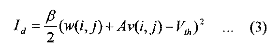


本実施の形態では、撮像装置の一例について図面を参照して説明する。
図7(A)に、実施の形態1で説明した画素回路を有する画素の構成を例示する。図7(A)に示す画素は、層261及び層262の積層構成を有する例である。
図11(A)は、本発明の一態様の撮像装置の画素にカラーフィルタ等を付加した例を示す斜視図である。当該斜視図では、複数の画素の断面もあわせて図示している。光電変換素子50が形成される層261上には、絶縁層280が形成される。絶縁層280は可視光に対して透光性の高い酸化シリコン膜などを用いることができる。また、パッシベーション層として窒化シリコン膜を積層してもよい。また、反射防止層として、酸化ハフニウムなどの誘電体膜を積層してもよい。
以下では、イメージセンサチップを収めたパッケージ及びカメラモジュールの一例について説明する。当該イメージセンサチップには、上記撮像装置の構成を用いることができる。
本発明の一態様に係る撮像装置を用いることができる電子機器として、表示機器、パーソナルコンピュータ、記録媒体を備えた画像記憶装置又は画像再生装置、携帯電話、携帯型を含むゲーム機、携帯データ端末、電子書籍端末、ビデオカメラ、デジタルスチルカメラ等のカメラ、ゴーグル型ディスプレイ(ヘッドマウントディスプレイ)、ナビゲーションシステム、音響再生装置(カーオーディオ、デジタルオーディオプレイヤー等)、複写機、ファクシミリ、プリンタ、プリンタ複合機、現金自動預け入れ払い機(ATM)、自動販売機などが挙げられる。
以上の実施の形態における各構成の説明について、以下に付記する。
各実施の形態に示す構成は、他の実施の形態に示す構成と適宜組み合わせて、本発明の一態様とすることができる。また、1つの実施の形態の中に、複数の構成例が示される場合は、互いに構成例を適宜組み合わせることが可能である。
本明細書等において、「第1」、「第2」、「第3」という序数詞は、構成要素の混同を避けるために付したものである。したがって、構成要素の数を限定するものではない。また、構成要素の順序を限定するものではない。また例えば、本明細書等の実施の形態の一において「第1」に言及された構成要素が、他の実施の形態、あるいは特許請求の範囲において「第2」に言及された構成要素とすることもありうる。また例えば、本明細書等の実施の形態の一において「第1」に言及された構成要素を、他の実施の形態、あるいは特許請求の範囲において省略することもありうる。
実施の形態について図面を参照しながら説明している。ただし、実施の形態は多くの異なる態様で実施することが可能であり、趣旨及びその範囲から逸脱することなく、その形態及び詳細を様々に変更し得ることは当業者であれば容易に理解される。したがって、本発明は、実施の形態の記載内容に限定して解釈されるものではない。なお、実施の形態の発明の構成において、同一部分又は同様な機能を有する部分には同一の符号を異なる図面間で共通して用い、その繰り返しの説明は省略する。
本明細書等において、トランジスタの接続関係を説明する際、「ソース又はドレインの一方」(又は第1電極、又は第1端子)、「ソース又はドレインの他方」(又は第2電極、又は第2端子)と表記している。これは、トランジスタのソースとドレインは、トランジスタの構造又は動作条件等によって変わるためである。なおトランジスタのソースとドレインの呼称については、ソース(ドレイン)端子や、ソース(ドレイン)電極等、状況に応じて適切に言い換えることができる。また、本明細書等では、ゲート以外の2つの端子を第1端子、第2端子と呼ぶ場合や、第3端子、第4端子と呼ぶ場合がある。また、本明細書等に記載するトランジスタが2つ以上のゲートを有するとき(この構成をデュアルゲート構造という場合がある)、それらのゲートを第1ゲート、第2ゲートと呼ぶ場合や、フロントゲート、バックゲートと呼ぶ場合がある。特に、「フロントゲート」という語句は、単に「ゲート」という語句に互いに言い換えることができる。また、「バックゲート」という語句は、単に「ゲート」という語句に互いに言い換えることができる。なお、ボトムゲートとは、トランジスタの作製時において、チャネル形成領域よりも先に形成される端子のことをいい、「トップゲート」とは、トランジスタの作製時において、チャネル形成領域よりも後に形成される端子のことをいう。
以下では、上記実施の形態中で言及した語句の定義について説明する。
半導体の不純物とは、例えば、半導体層を構成する主成分以外をいう。例えば、濃度が0.1原子%未満の元素は不純物である。不純物が含まれることにより、例えば、半導体にDOS(Density of States)が形成されることや、キャリア移動度が低下することや、結晶性が低下することなどが起こる場合がある。半導体が酸化物半導体である場合、半導体の特性を変化させる不純物としては、例えば、第1族元素、第2族元素、第13族元素、第14族元素、第15族元素、主成分以外の遷移金属などがあり、特に、例えば、水素(水にも含まれる)、リチウム、ナトリウム、シリコン、ホウ素、リン、炭素、窒素などがある。酸化物半導体の場合、例えば水素などの不純物の混入によって酸素欠損を形成する場合がある。また、半導体がシリコン層である場合、半導体の特性を変化させる不純物としては、例えば、酸素、水素を除く第1族元素、第2族元素、第13族元素、第15族元素などがある。
本明細書において、トランジスタとは、ゲートと、ドレインと、ソースとを含む少なくとも三つの端子を有する素子である。そして、ドレイン(ドレイン端子、ドレイン領域又はドレイン電極)とソース(ソース端子、ソース領域又はソース電極)の間にチャネル形成領域を有する。ゲート−ソース間にしきい値電圧を超える電圧を与えることによって、チャネル形成領域にチャネルが形成され、ソース‐ドレイン間に電流を流すことができる。
本明細書等において、スイッチとは、導通状態(オン状態)、又は、非導通状態(オフ状態)になり、電流を流すか流さないかを制御する機能を有するものをいう。又は、スイッチとは、電流を流す経路を選択する機能を有するものをいう。
本明細書等において、XとYとが接続されている、と記載する場合は、XとYとが電気的に接続されている場合と、XとYとが機能的に接続されている場合と、XとYとが直接接続されている場合とを含むものとする。したがって、所定の接続関係、例えば、図又は文章に示された接続関係に限定されず、図又は文章に示された接続関係以外のものも含むものとする。
本明細書において、「平行」とは、二つの直線が−10°以上10°以下の角度で配置されている状態をいう。したがって、−5°以上5°以下の場合も含まれる。また、「略平行」とは、二つの直線が−30°以上30°以下の角度で配置されている状態をいう。また、「垂直」とは、二つの直線が80°以上100°以下の角度で配置されている状態をいう。したがって、85°以上95°以下の場合も含まれる。また、「略垂直」とは、二つの直線が60°以上120°以下の角度で配置されている状態をいう。
Claims (13)
- ニューラルネットワークインターフェースを有する撮像装置であって、
前記撮像装置は、画素領域と、第1の回路と、第2の回路と、第3の回路と、第4の回路と、第1の信号線Wxと、を有し、
前記画素領域は、複数の画素を有し、
前記画素は、第1のトランジスタを有し、
前記第4の回路は、前記ニューラルネットワークインターフェースを有し、
前記画素は、前記第1の信号線Wxを介して前記第3の回路と電気的に接続され、
前記第3の回路は、前記第4の回路と電気的に接続され、
前記第1の回路は、前記画素に走査信号を与える機能を有し、
前記第2の回路は、前記走査信号によって選択される前記画素に重み電位を与える機能を有し、
前記画素は、光から光電変換することで第1の信号を取得する機能を有し、
前記画素は、前記第1のトランジスタによって前記第1の信号と、前記重み電位と、を乗算する機能を有し、
前記第1のトランジスタは、前記第1の信号と、前記重み電位との乗算項と、第1のオフセット項と、第2のオフセット項とを生成する機能を有し、
前記第3の回路は、前記第1のオフセット項を減算する機能を有し、
前記第4の回路は、前記第2のオフセット項を減算する機能を有し、
前記第4の回路は、前記乗算項を判定する機能を有し、
前記第4の回路は、前記ニューラルネットワークインターフェースを介して判定結果を出力することを特徴とする撮像装置。 - 請求項1において、
前記第2の回路は、さらに、前記走査信号によって選択される前記画素にオフセット電位を与える機能を有し、
前記画素は、前記第1の信号に前記オフセット電位を加えることで第2の信号を生成する機能を有し、
前記画素は、前記オフセット電位に前記重み電位を加えることで第3の信号を生成する機能を有し、
前記画素は、前記第1の信号に前記オフセット電位と前記重み電位とを加えることで第4の信号を生成する機能を有し、
前記第1のトランジスタは、前記第2の信号を任意の倍率で乗算し第5の信号を生成する機能を有し、
前記第1のトランジスタは、前記第3の信号を任意の倍率で乗算し第6の信号を生成する機能を有し、
前記第1のトランジスタは、前記第4の信号を任意の倍率で乗算し第7の信号を生成する機能を有し、
前記第3の回路は、前記第2の信号を記憶する機能を有し、
前記第3の回路は、前記第7の信号と前記第5の信号とを演算することで第8の信号を生成する機能を有し、
前記第4の回路は、前記第8の信号を記憶する機能を有し、
前記第4の回路は、前記第8の信号と前記第6の信号とを演算することで第9の信号を生成する機能を有し、
前記第9の信号には、前記第1の信号と、前記重み電位との乗算項が出力され、
前記第4の回路は、前記第9の信号を判定する機能を有し、
前記第4の回路は、前記ニューラルネットワークインターフェースを介して判定結果を出力することを特徴とする撮像装置。 - 請求項1又は請求項2において、
前記撮像装置は、さらに、アナログデジタル変換回路と、信号線Pioと、配線VRSと、を有し、
前記画素は、前記信号線Pioを介して前記第1のデータを前記アナログデジタル変換回路に出力する機能を有し、
前記画素には、前記信号線Pioを介して前記配線VRSに与えられる第1の電位が入力される機能を有し、
前記画素は、前記信号線Pioを介して前記配線VRSに与えられる第1の電位が入力されるときニューラルネットワークのニューロンとして機能することを特徴とする撮像装置。 - 請求項1又は請求項2において、
前記撮像装置は、さらに、配線VPD、配線VDM、信号線G1、信号線G2、信号線G3、信号線Tx、信号線Res、信号線S1、及び信号線S2を有し、
前記画素は、光電変換素子、第2のトランジスタ、第3のトランジスタ、第4のトランジスタ、第5のトランジスタ、第6のトランジスタ、第7のトランジスタ、第1の容量素子、第2の容量素子、及び第3の容量素子を有し、
前記第1の回路は、前記信号線G1を介して画素と電気的に接続され、
前記第1の回路は、前記信号線G2を介して画素と電気的に接続され、
前記第1の回路は、前記信号線G3を介して画素と電気的に接続され、
前記第2の回路は、前記信号線S1を介して画素と電気的に接続され、
前記第2の回路は、前記信号線S2を介して画素と電気的に接続され、
前記光電変換素子の電極の一方は、前記配線VPDと電気的に接続され、
前記光電変換素子の電極の他方は、前記第2のトランジスタのソース又はドレインの一方と電気的に接続され、
前記第2のトランジスタのゲートは、前記信号線Txと電気的に接続され、
前記第2のトランジスタのソース又はドレインの他方は、前記第3のトランジスタのソース又はドレインの一方と、前記第4のトランジスタのゲートと、前記第1の容量素子の電極の一方と電気的に接続され、
前記第3のトランジスタのソース又はドレインの他方は、前記配線VRSと電気的に接続され、
前記第3のトランジスタのゲートは、前記信号線Resと電気的に接続され、
前記第4のトランジスタのソース又はドレインの一方は、前記配線VDMと電気的に接続され、
前記第4のトランジスタのソース又はドレインの他方は、前記第5のトランジスタのソース又はドレインの一方と、前記第2の容量素子の電極の一方と電気的に接続され、
前記第5のトランジスタのソース又はドレインの他方は、前記配線Pioと電気的に接続され、
前記第5のトランジスタのゲートは、前記信号線G3と電気的に接続され、
前記第2の容量素子の他方の電極は、前記第1のトランジスタのゲートと、前記第6のトランジスタのソース又はドレインの一方と、前記第3の容量素子の電極の一方と電気的に接続され、
前記第1のトランジスタのソース又はドレインの一方は、前記第1の信号線Wxと電気的に接続され、
前記第6のトランジスタのソース又はドレインの他方は、前記信号線S1と電気的に接続され、
前記第6のトランジスタのゲートは、前記信号線G1と電気的に接続され、
前記第3の容量素子の他方の電極は、前記第7のトランジスタのソース又はドレインの一方と電気的に接続され、
前記第7のトランジスタのソース又はドレインの他方は、前記信号線S2と電気的に接続され、
前記第7のトランジスタのゲートは、前記信号線G2と電気的に接続されることで形成されることを特徴とする撮像装置。 - 請求項4において、
前記撮像装置は、さらに、信号線Csw、信号線Cswb、信号線Eabs、信号線Osp、信号線Ewx、信号線Mac、及び配線VIVを有し、
前記第3の回路は、カレントミラー回路と、記憶回路と、出力回路と、を有し、
前記カレントミラー回路は、第8のトランジスタ、第9のトランジスタ、第10のトランジスタ、第11のトランジスタ、及び第12のトランジスタを有し、
前記記憶回路は、第13のトランジスタ、第14のトランジスタ、第15のトランジスタ、及び第4の容量素子を有し、
前記出力回路は、第16のトランジスタ、及び抵抗素子R1を有し、
前記配線VDMは、前記第8のトランジスタのソース又はドレインの一方と、前記第9のトランジスタのソース又はドレインの一方と電気的に接続され、
前記第8のトランジスタのゲートは、前記第9のトランジスタのゲートと、前記第10のトランジスタのソース又はドレインの一方と、前記第11のトランジスタのソース又はドレインの一方と電気的に接続され、
前記第8のトランジスタのソース又はドレインの他方は、前記第10のトランジスタのソース又はドレインの他方と、前記第12のトランジスタのソース又はドレインの一方と電気的に接続され、
前記第10のトランジスタのゲートは、前記信号線Cswbと電気的に接続され、
前記第11のトランジスタのゲートは、前記信号線Cswと電気的に接続され、
前記第12のトランジスタのゲートは、前記信号線Eabsと電気的に接続され、
前記第12のトランジスタのソース又はドレインの他方は、前記第1の信号線Wxと、前記第15のトランジスタのソース又はドレインの一方と電気的に接続され、
前記第9のトランジスタのソース又はドレインの他方は、前記第11のトランジスタのソース又はドレインの他方と、前記第13のトランジスタのソース又はドレインの一方と、前記第14のトランジスタの一方と電気的に接続され、
前記第14のトランジスタのゲートは、前記信号線Ospと電気的に接続され、
前記第14のトランジスタのソース又はドレインの他方は、前記第15のトランジスタのソース又はドレインの一方と、前記第4の容量素子の電極の一方と、前記第13のトランジスタのゲートと電気的に接続され、
前記第15のトランジスタのゲートは、前記信号線Resと電気的に接続され、
前記第16のトランジスタのソース又はドレインの他方は、前記抵抗素子R1の電極の一方と、前記信号線Macと電気的に接続され、
前記第16のトランジスタのゲートは、前記信号線Ewxと電気的に接続され、
前記抵抗素子R1の電極の他方は、前記配線VIVに電気的に接続されることを特徴とする撮像装置。 - 請求項1又は請求項2において、
前記撮像装置は、さらに、信号線Sh、信号線CL、信号線Out、配線VCDS、及び配線JDを有し、
前記第4の回路は、CDS回路と、判定回路と、を有し、
前記CDS回路は、第5の容量素子、第6の容量素子、オペアンプOP1、及び第17のトランジスタを有し、
前記判定回路は、第7の容量素子、オペアンプOP2、及び第18のトランジスタを有し、
前記信号線Macは、前記第5の容量素子の電極の一方と電気的に接続され、
前記オペアンプOP1の第1の入力端子は、前記第5の容量素子の電極の他方と、前記第6の容量素子の電極の一方と、前記第17のトランジスタのソース又はドレインの一方と電気的に接続され、
前記第17のトランジスタのゲートは、前記信号線CLと電気的に接続され、
前記オペアンプOP1の第2の入力端子は、前記配線VCDSと電気的に接続され、
前記オペアンプOP1の出力端子は、前記第6の容量素子の電極の他方と、前記第17のトランジスタのソース又はドレインの他方と、前記第18のトランジスタのソース又はドレインの一方と電気的に接続され、
前記第18のトランジスタのゲートは、前記信号線Shと電気的に接続され、
前記第18のトランジスタのソース又はドレインの他方は、前記オペアンプOP2の第1の入力端子と、前記第7の容量素子の電極の一方と電気的に接続され、
前記オペアンプOP2の第2の入力端子は、前記配線JDと電気的に接続され、
前記オペアンプOP2の出力端子は、前記信号線Outと電気的に接続され、
前記信号線Outは、前記ニューラルネットワークと接続されることを特徴とする撮像装置。 - 請求項1又は請求項2において、
前記撮像装置は、さらに、前記第2の信号線Wxと、信号線Bsel1と、スイッチBswと、を有し、
前記スイッチBswは、前記配線Bselに与えられる信号によって前記第1の信号線Wxと前記第2の信号線Wxとを電気的に接続する機能を有し、
前記第3の回路には、前記第1の信号線Wxに接続される複数の前記画素と、前記第2の信号線Wxに接続される複数の前記画素とから、複数の前記第5の信号と、複数の前記第6の信号と、複数の前記第7の信号とが与えられる機能を有し、
第3の回路は、それぞれの画素から与えられる第5の信号、第6の信号、及び第7の信号を加算してから、第1のオフセット項を減算する機能を有し、
前記撮像装置は、前記スイッチBswに与える信号によって複数の前記画素の選択範囲を選択できる機能を有し、
前記撮像装置は、前記画素の選択範囲に応じたプーリング処理がされることを特徴とする撮像装置。 - 請求項4において、
前記光電変換素子は、セレン又はセレンを含む化合物を有する撮像装置。 - 請求項4において、
前記第1のトランジスタ、前記第2のトランジスタ、前記第4のトランジスタ、前記第6のトランジスタ、及び前記第7のトランジスタのいずれか一もしくは複数が、チャネル形成領域に金属酸化物を有する撮像装置。 - 請求項4において、
前記第13のトランジスタは、前記第5のトランジスタのチャネル長及びチャネル幅と同じ大きさを有することを特徴とする撮像装置。 - 請求項5において、
前記配線VIVに与えられる第2の電位は、前記配線VDMに与えられる第3の電位よりも小さいことを特徴とする撮像装置。 - 請求項10において、
前記金属酸化物は、Inと、Znと、M(MはAl、Ti、Ga、Sn、Y、Zr、La、Ce、Nd又はHf)と、を有する撮像装置。 - 請求項1又は請求項2に記載の前記撮像装置と、表示装置と、を有する電子機器。
Priority Applications (5)
| Application Number | Priority Date | Filing Date | Title |
|---|---|---|---|
| KR1020207003452A KR20200028967A (ko) | 2017-07-14 | 2018-07-02 | 촬상 장치 및 전자 기기 |
| US16/628,914 US10951850B2 (en) | 2017-07-14 | 2018-07-02 | Imaging device and electronic device |
| JP2019529317A JP7144413B2 (ja) | 2017-07-14 | 2018-07-02 | 撮像装置 |
| CN201880045145.XA CN110832845B (zh) | 2017-07-14 | 2018-07-02 | 摄像装置及电子设备 |
| EP18831474.4A EP3654635A4 (en) | 2017-07-14 | 2018-07-02 | IMAGING DEVICE AND ELECTRONIC DEVICE |
Applications Claiming Priority (2)
| Application Number | Priority Date | Filing Date | Title |
|---|---|---|---|
| JP2017137910 | 2017-07-14 | ||
| JP2017-137910 | 2017-07-14 |
Publications (1)
| Publication Number | Publication Date |
|---|---|
| WO2019012369A1 true WO2019012369A1 (ja) | 2019-01-17 |
Family
ID=65002562
Family Applications (1)
| Application Number | Title | Priority Date | Filing Date |
|---|---|---|---|
| PCT/IB2018/054888 WO2019012369A1 (ja) | 2017-07-14 | 2018-07-02 | 撮像装置、及び電子機器 |
Country Status (6)
| Country | Link |
|---|---|
| US (1) | US10951850B2 (ja) |
| EP (1) | EP3654635A4 (ja) |
| JP (1) | JP7144413B2 (ja) |
| KR (1) | KR20200028967A (ja) |
| CN (1) | CN110832845B (ja) |
| WO (1) | WO2019012369A1 (ja) |
Cited By (6)
| Publication number | Priority date | Publication date | Assignee | Title |
|---|---|---|---|---|
| WO2020250095A1 (ja) * | 2019-06-14 | 2020-12-17 | 株式会社半導体エネルギー研究所 | 撮像装置および電子機器 |
| WO2021033065A1 (ja) * | 2019-08-22 | 2021-02-25 | 株式会社半導体エネルギー研究所 | 撮像装置および電子機器 |
| WO2021048695A1 (ja) * | 2019-09-13 | 2021-03-18 | 株式会社半導体エネルギー研究所 | 撮像装置、及びその駆動方法 |
| WO2021053449A1 (ja) * | 2019-09-20 | 2021-03-25 | 株式会社半導体エネルギー研究所 | 撮像システムおよび電子機器 |
| WO2021165781A1 (ja) * | 2020-02-20 | 2021-08-26 | 株式会社半導体エネルギー研究所 | 撮像装置、電子機器および移動体 |
| WO2021191719A1 (ja) * | 2020-03-27 | 2021-09-30 | 株式会社半導体エネルギー研究所 | 撮像装置および電子機器 |
Families Citing this family (1)
| Publication number | Priority date | Publication date | Assignee | Title |
|---|---|---|---|---|
| CN109786399B (zh) * | 2017-11-13 | 2022-04-05 | 睿生光电股份有限公司 | 检测装置 |
Citations (3)
| Publication number | Priority date | Publication date | Assignee | Title |
|---|---|---|---|---|
| JP2016123087A (ja) | 2014-12-10 | 2016-07-07 | 株式会社半導体エネルギー研究所 | 半導体装置および電子機器 |
| JP2017054502A (ja) * | 2015-08-31 | 2017-03-16 | 株式会社半導体エネルギー研究所 | 半導体装置、又は該半導体装置を有する電子機器 |
| JP2017063420A (ja) * | 2015-09-25 | 2017-03-30 | 株式会社半導体エネルギー研究所 | 半導体装置 |
Family Cites Families (9)
| Publication number | Priority date | Publication date | Assignee | Title |
|---|---|---|---|---|
| JP3642591B2 (ja) * | 1994-11-29 | 2005-04-27 | 株式会社日立メディコ | 画像処理装置 |
| JP3810725B2 (ja) * | 2001-09-21 | 2006-08-16 | 株式会社半導体エネルギー研究所 | 発光装置及び電子機器 |
| US7151844B2 (en) * | 2001-12-06 | 2006-12-19 | General Motors Corporation | Image sensor method and apparatus having hardware implemented edge detection processing |
| US7215370B2 (en) * | 2003-07-23 | 2007-05-08 | Alphaplus Semiconductor Inc. | Pseudo-BJT based retinal focal-plane sensing system |
| CN104520896B (zh) * | 2012-01-27 | 2017-09-29 | 韩国科学技术院 | 视觉神经电路装置及利用视觉神经电路装置的视觉神经模仿系统 |
| US9762834B2 (en) * | 2014-09-30 | 2017-09-12 | Qualcomm Incorporated | Configurable hardware for computing computer vision features |
| US20160328642A1 (en) * | 2015-05-06 | 2016-11-10 | Indiana University Research And Technology Corporation | Sensor signal processing using an analog neural network |
| KR102631381B1 (ko) * | 2016-11-07 | 2024-01-31 | 삼성전자주식회사 | 컨볼루션 신경망 처리 방법 및 장치 |
| US11403833B2 (en) | 2017-05-18 | 2022-08-02 | Semiconductor Energy Laboratory Co., Ltd. | Image detection module and information management system |
-
2018
- 2018-07-02 JP JP2019529317A patent/JP7144413B2/ja active Active
- 2018-07-02 EP EP18831474.4A patent/EP3654635A4/en not_active Withdrawn
- 2018-07-02 KR KR1020207003452A patent/KR20200028967A/ko not_active Application Discontinuation
- 2018-07-02 US US16/628,914 patent/US10951850B2/en active Active
- 2018-07-02 CN CN201880045145.XA patent/CN110832845B/zh active Active
- 2018-07-02 WO PCT/IB2018/054888 patent/WO2019012369A1/ja unknown
Patent Citations (3)
| Publication number | Priority date | Publication date | Assignee | Title |
|---|---|---|---|---|
| JP2016123087A (ja) | 2014-12-10 | 2016-07-07 | 株式会社半導体エネルギー研究所 | 半導体装置および電子機器 |
| JP2017054502A (ja) * | 2015-08-31 | 2017-03-16 | 株式会社半導体エネルギー研究所 | 半導体装置、又は該半導体装置を有する電子機器 |
| JP2017063420A (ja) * | 2015-09-25 | 2017-03-30 | 株式会社半導体エネルギー研究所 | 半導体装置 |
Non-Patent Citations (1)
| Title |
|---|
| See also references of EP3654635A4 |
Cited By (8)
| Publication number | Priority date | Publication date | Assignee | Title |
|---|---|---|---|---|
| WO2020250095A1 (ja) * | 2019-06-14 | 2020-12-17 | 株式会社半導体エネルギー研究所 | 撮像装置および電子機器 |
| JP7480137B2 (ja) | 2019-06-14 | 2024-05-09 | 株式会社半導体エネルギー研究所 | 撮像装置および電子機器 |
| WO2021033065A1 (ja) * | 2019-08-22 | 2021-02-25 | 株式会社半導体エネルギー研究所 | 撮像装置および電子機器 |
| WO2021048695A1 (ja) * | 2019-09-13 | 2021-03-18 | 株式会社半導体エネルギー研究所 | 撮像装置、及びその駆動方法 |
| WO2021053449A1 (ja) * | 2019-09-20 | 2021-03-25 | 株式会社半導体エネルギー研究所 | 撮像システムおよび電子機器 |
| US11956570B2 (en) | 2019-09-20 | 2024-04-09 | Semiconductor Energy Laboratory Co., Ltd. | Imaging system and electronic device |
| WO2021165781A1 (ja) * | 2020-02-20 | 2021-08-26 | 株式会社半導体エネルギー研究所 | 撮像装置、電子機器および移動体 |
| WO2021191719A1 (ja) * | 2020-03-27 | 2021-09-30 | 株式会社半導体エネルギー研究所 | 撮像装置および電子機器 |
Also Published As
| Publication number | Publication date |
|---|---|
| US10951850B2 (en) | 2021-03-16 |
| US20200145600A1 (en) | 2020-05-07 |
| CN110832845B (zh) | 2022-07-05 |
| CN110832845A (zh) | 2020-02-21 |
| JP7144413B2 (ja) | 2022-09-29 |
| JPWO2019012369A1 (ja) | 2020-07-27 |
| EP3654635A4 (en) | 2020-12-30 |
| KR20200028967A (ko) | 2020-03-17 |
| EP3654635A1 (en) | 2020-05-20 |
Similar Documents
| Publication | Publication Date | Title |
|---|---|---|
| JP7144413B2 (ja) | 撮像装置 | |
| JP7322239B2 (ja) | 撮像装置および電子機器 | |
| JP7335990B2 (ja) | 撮像装置 | |
| JP7224429B2 (ja) | 撮像装置、及び電子機器 | |
| JP7217227B2 (ja) | 撮像装置、及び電子機器 | |
| WO2020222059A1 (ja) | 撮像装置、その動作方法、および電子機器 | |
| WO2021191719A1 (ja) | 撮像装置および電子機器 | |
| US20220359592A1 (en) | Imaging device and electronic device | |
| JP2019009640A (ja) | 撮像装置および電子機器 | |
| WO2021214616A1 (ja) | 撮像装置 | |
| WO2021209868A1 (ja) | 撮像装置および電子機器 | |
| WO2021165781A1 (ja) | 撮像装置、電子機器および移動体 | |
| WO2021053449A1 (ja) | 撮像システムおよび電子機器 | |
| WO2020250095A1 (ja) | 撮像装置および電子機器 | |
| JP2018164139A (ja) | 撮像装置および電子機器 |
Legal Events
| Date | Code | Title | Description |
|---|---|---|---|
| 121 | Ep: the epo has been informed by wipo that ep was designated in this application |
Ref document number: 18831474 Country of ref document: EP Kind code of ref document: A1 |
|
| ENP | Entry into the national phase |
Ref document number: 2019529317 Country of ref document: JP Kind code of ref document: A |
|
| NENP | Non-entry into the national phase |
Ref country code: DE |
|
| ENP | Entry into the national phase |
Ref document number: 20207003452 Country of ref document: KR Kind code of ref document: A |
|
| ENP | Entry into the national phase |
Ref document number: 2018831474 Country of ref document: EP Effective date: 20200214 |