WO2021009956A1 - 温度補償回路及び温度補償水晶発振器 - Google Patents
温度補償回路及び温度補償水晶発振器 Download PDFInfo
- Publication number
- WO2021009956A1 WO2021009956A1 PCT/JP2020/006087 JP2020006087W WO2021009956A1 WO 2021009956 A1 WO2021009956 A1 WO 2021009956A1 JP 2020006087 W JP2020006087 W JP 2020006087W WO 2021009956 A1 WO2021009956 A1 WO 2021009956A1
- Authority
- WO
- WIPO (PCT)
- Prior art keywords
- temperature
- circuit
- temperature side
- crystal oscillator
- low
- Prior art date
- Legal status (The legal status is an assumption and is not a legal conclusion. Google has not performed a legal analysis and makes no representation as to the accuracy of the status listed.)
- Ceased
Links
Images





Classifications
-
- H—ELECTRICITY
- H03—ELECTRONIC CIRCUITRY
- H03B—GENERATION OF OSCILLATIONS, DIRECTLY OR BY FREQUENCY-CHANGING, BY CIRCUITS EMPLOYING ACTIVE ELEMENTS WHICH OPERATE IN A NON-SWITCHING MANNER; GENERATION OF NOISE BY SUCH CIRCUITS
- H03B5/00—Generation of oscillations using amplifier with regenerative feedback from output to input
- H03B5/30—Generation of oscillations using amplifier with regenerative feedback from output to input with frequency-determining element being electromechanical resonator
- H03B5/32—Generation of oscillations using amplifier with regenerative feedback from output to input with frequency-determining element being electromechanical resonator being a piezoelectric resonator
Definitions
- the present invention relates to a temperature compensation circuit and a temperature compensation crystal oscillator.
- the resonance frequency of the crystal vibrating element (Crystal Resonator) included in the crystal oscillator (Crystal Oscillator) changes according to the temperature.
- a temperature-compensated crystal oscillator Tempoture Compensated crystal Oscillator, hereinafter sometimes referred to as "TCXO”
- TCXO Temperatur Compensated crystal Oscillator
- VXO Voltage Controlled crystal Oscillator
- It has a temperature compensation circuit that generates a voltage applied to the oscillator. With this temperature compensation circuit, it is possible to control the oscillation frequency of the temperature compensation type crystal oscillator to be constant even if the temperature changes.
- Patent Document 1 describes a TCXO that applies a compensation voltage to the VCXO by adding a plurality of voltages output from a plurality of Nth-order function generation circuits.
- the temperature compensation circuit including the Nth function generation circuit includes a circuit (primary adjustment circuit) that rotationally corrects the primary compensation voltage output from the primary function generation circuit.
- a circuit primary adjustment circuit
- the slope (rate of change) of the primary component of the frequency temperature characteristic of the crystal vibrating element is not constant over the entire operating temperature range of the TCXO.
- the present invention has been invented in view of the above problems, and an object of the present invention is to suppress a correction error.
- the resonance frequency is maximized at the first temperature, the resonance frequency is minimized at the second temperature higher than the first temperature, and the reference temperature is higher than the first temperature and lower than the second temperature.
- the low temperature side circuit When the temperature of the high temperature side circuit that outputs the high temperature side compensation signal to cancel the temperature change and the temperature of the crystal oscillator is lower than the reference temperature, the low temperature side circuit is operated and the temperature of the crystal oscillator is higher than the reference temperature. In some cases, it includes a switching circuit that operates the high temperature side circuit.
- the low temperature side circuit outputs the low temperature side compensation signal by adding the signals of a plurality of integer order components to the low temperature side primary adjustment circuit that adjusts the inclination of the primary component of the low temperature side compensation signal. Includes a compensation circuit.
- the high temperature side circuit outputs the high temperature side compensation signal by adding the signals of a plurality of integer order components to the high temperature side primary adjustment circuit that adjusts the inclination of the primary component of the high temperature side compensation signal. Includes a compensation circuit.
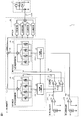
- FIG. 1 is a diagram showing a configuration of a temperature-compensated crystal oscillator according to the first embodiment.
- the temperature-compensated crystal oscillator (TCXO) 1 includes a voltage-controlled crystal oscillator (VCXO) 2, which is a frequency-variable crystal oscillator, a first temperature detection circuit 3-1 and a second temperature detection circuit 3-2, and temperature compensation. Includes circuit 4.
- VCXO voltage-controlled crystal oscillator
- the VCXO2 includes a crystal oscillator 11, a resistor 12 as a feedback resistor, an inverter (inverting) circuit 13 as an amplifier circuit, a variable capacitance circuit 14, and a capacitor 15.
- the crystal vibrating element 11 includes an AT-cut crystal piece and excitation electrodes provided on both main surfaces of the crystal piece.
- the variable capacitance circuit 14 is a variable capacitance diode (varicap), but the present disclosure is not limited to this.
- the variable capacitance circuit 14 is composed of a plurality of capacitors, and the connection state of one or a plurality of capacitors may be selected based on the control voltage VCTR described later.
- the crystal vibrating element 11, the resistor 12, and the inverter circuit 13 are connected in parallel.
- the variable capacitance circuit 14 is electrically connected between one end of the crystal vibrating element 11 and the reference potential.
- the reference potential is exemplified by the ground potential, but the present disclosure is not limited to this.
- the capacitor 15 is electrically connected between the other end of the crystal vibrating element 11 and the reference potential.
- the capacitor 15 may be replaced with a variable capacitance circuit. In this case, the replaced variable capacitance circuit is connected to the temperature compensation circuit 4.
- the crystal vibrating element 11 has a characteristic that the resonance frequency changes according to the temperature.
- the ideal waveform indicated by the frequency / temperature characteristic may be hereinafter referred to as a "model waveform”.
- FIG. 2 is a diagram showing a change in the resonance frequency deviation with respect to a temperature change of the crystal vibrating element.
- Model waveform 200 showing the change in the resonance frequency deviation against temperature change of the quartz crystal resonator element 11 of the AT-cut becomes a maximum at temperatures T 1 becomes a minimum at a higher temperature T 2 than the temperatures T 1, temperatures T 1 than the high and the temperature T It is a waveform similar to a cubic curve in which an inflection point exists at a reference temperature T 0 lower than 2 .
- the temperature T 1 is exemplified by a temperature of ⁇ 20 ° C. or higher and ⁇ 10 ° C. or lower, for example, ⁇ 15 ° C., but the present disclosure is not limited thereto.
- the temperature T 2 is exemplified by a temperature of 65 ° C. or higher and 75 ° C. or lower, for example, 70 ° C., but the present disclosure is not limited thereto.
- the reference temperature T 0 is a temperature that serves as a reference for the oscillation frequency of the VCXO2, and a temperature of 25 ° C. or higher and 30 ° C. or lower is exemplified, but the present disclosure is not limited thereto.
- the reference temperature T 0 may be 27 ° C. (300 Kelvin).
- the reference temperature T 0 may be the central temperature in the temperature range of temperature T 1 or higher and temperature T 2 or lower.
- the temperature compensation circuit 4 outputs a control voltage VCTR that stabilizes the frequency temperature characteristic to the VCXO2 by canceling the change in the frequency temperature characteristic of the crystal vibrating element 11.
- the control voltage VCTR has a waveform similar to a cubic curve, which becomes a minimum at a temperature T 1 , a maximum at a temperature T 2 , and an inflection point at a reference temperature T 0 .
- the capacitance of the variable capacitance circuit 14 changes according to the control voltage VCTR.
- the time constant of the VCXO2 changes, so that the oscillation frequency of the VCXO2 changes.
- the temperature compensation circuit 4 cancels the temperature change of the oscillation frequency of the VCXO2 by the change of the time constant of the VCXO2.
- the temperature compensation circuit 4 includes an analog circuit capable of reproducing an ideal waveform of a change in resonance frequency with respect to a change in temperature in the crystal vibrating element 11, and generates a signal for suppressing a temperature change in the oscillation frequency of VCXO2 based on this ideal waveform. ..
- the temperature compensation circuit 4 can be controlled so that the oscillation frequency of the VCXO2 becomes constant.
- the temperature compensation circuit 4 performs temperature compensation by an Nth-order compensation circuit (N is a predetermined integer of 3 or more). Therefore, before the explanation of the temperature compensation circuit 4, the principle of temperature compensation by the Nth order compensation circuit will be described.
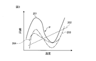
- FIG. 3 is a diagram for simplifying and explaining the principle of temperature compensation by the Nth order compensation circuit.
- Waveform 201 is an example of a waveform in which the voltage applied to VCXO2 is simplified. Actually, the voltage of the waveform obtained by inverting the waveform 201 upside down is applied to the VCXO2. Waveform 201 has an inflection point P.
- the waveform 201 is output from the waveform 202 which simplifies the primary compensation voltage output from the primary compensation circuit, the waveform 203 which simplifies the tertiary compensation voltage output from the tertiary compensation circuit, and the fifth compensation circuit.
- the fifth-order compensation voltage to be generated can be represented by the sum of the simplified waveform 204 and. Further, a fourth-order compensation voltage or a sixth-order or higher compensation voltage may be added.
- FIG. 4 is a diagram for explaining the output waveform of the temperature detection circuit in a simplified manner.
- the waveform 205 is a linear waveform having a polarity (rising to the right) in which the voltage increases as the temperature increases.
- the output waveform of the temperature detection circuit may be a linear waveform having a polarity (downward to the right) in which the voltage decreases as the temperature increases.
- FIG. 5 is a diagram for explaining the operation of the primary adjustment circuit in a simplified manner.
- the primary adjustment circuit can increase the slope of the waveform 205, as shown by arrow 206, for example, by multiplying the primary compensation voltage by a gain greater than 1. Further, for example, in the primary adjustment circuit, the slope of the waveform 205 can be reduced as shown by arrow 207 by multiplying the primary compensation voltage by a gain larger than 0 and smaller than 1. As a result, the primary adjustment circuit can match the slope of the waveform 205 with the slope of the primary component of the model waveform 200.
- the low temperature is defined as a temperature range lower than the reference temperature T 0 .
- the high temperature is defined as a temperature range higher than the reference temperature T 0 .
- the temperature compensation circuit 4 includes a low temperature side primary adjustment circuit 51 that corrects the primary compensation voltage on the low temperature side and a high temperature side primary adjustment circuit 53 that corrects the primary compensation voltage on the high temperature side. did.
- the low temperature side primary adjustment circuit 51 can suppress the correction error of the low temperature side primary component
- the high temperature side primary adjustment circuit 53 suppresses the correction error of the high temperature side primary component. it can. Therefore, the temperature compensation circuit 4 can suppress the correction error of the primary component in the entire operating temperature range.
- the first temperature detection circuit 3-1 and the second temperature detection circuit 3-2 are arranged in the vicinity of the crystal vibration element 11, detect the temperature of the VCXO2, and represent the temperature state of the VCXO2.
- VS1 and VS2 are output to the temperature compensation circuit 4, respectively.
- the voltages VS1 and VS2 correspond to the "temperature signal" of the present disclosure.
- the first temperature detection circuit 3-1 and the second temperature detection circuit 3-2 output voltages VS1 and VS2 having polarities (downward to the right) that decrease as the temperature increases. Disclosure is not limited to this.
- the first temperature detection circuit 3-1 and the second temperature detection circuit 3-2 may output voltages VS1 and VS2 having polarities (rising upward) as the temperature rises.
- the first temperature detection circuit 3-1 includes a temperature sensor 21 and a differential amplifier 22.
- the temperature sensor 21 is electrically connected between the non-inverting input terminal of the differential amplifier 22 and the reference potential.
- the inverting input terminal of the differential amplifier 22 is electrically connected to the reference potential.
- the second temperature detection circuit 3-2 includes a temperature sensor 23 and a differential amplifier 24, and has the same circuit configuration as the first temperature detection circuit 3-1.
- the slope of the voltage VS1 and the slope of the voltage VS2 may be the same or different.
- the first temperature detection circuit 3-1 is calibrated to match the primary component on the low temperature side of the model waveform 200
- the second temperature detection circuit 3-2 is on the high temperature side of the model waveform 200. It should be calibrated to match the primary component. As a result, the accuracy of temperature compensation can be further improved on each of the low temperature side and the high temperature side.
- the temperature compensation circuit 4 includes a low temperature side circuit 31, a high temperature side circuit 32, a switching circuit 33, and an adjusting circuit 34.
- Cold side circuit 31 is a temperature range lower than the reference temperature T 0, on the basis of the voltage VS1, and outputs the low-temperature-side compensation voltage VL for canceling the temperature change of the oscillation frequency of VCXO2.
- High-temperature side circuit 32 is a temperature range higher than the reference temperature T 0, on the basis of the voltage VS2, and outputs the high-temperature-side compensation voltage VH to cancel the temperature change of the oscillation frequency of VCXO2.
- the switching circuit 33 operates the low temperature side circuit 31 and does not operate the high temperature side circuit 32 in a temperature range lower than the reference temperature T 0 . Further, the switching circuit 33 operates the high temperature side circuit 32 and does not operate the low temperature side circuit 31 in a temperature range higher than the reference temperature T 0 .
- the adjustment circuit 34 adjusts the low temperature side compensation voltage VL and the high temperature side compensation voltage VH, and outputs the adjusted control voltage VCTR to the VCXO2.
- the switching circuit 33 operates the low temperature side circuit 31 and does not operate the high temperature side circuit 32 when the temperature of the VCXO2 is the reference temperature T 0. Not limited. Switching circuit 33, when the temperature of VCXO2 is the reference temperature T 0, to operate the high-temperature side circuit 32, it is also possible not to operate the low-temperature side circuit 31.
- the switching circuit 33 includes comparators 41 and 42.
- the voltage VS1 is input to the non-inverting input terminal of the comparator 41.
- the reference voltage VT0 is input from the power supply circuit to the inverting input terminal of the comparator 41.
- Reference voltage VT0 in the case where the temperature of VCXO2 of the reference temperature T 0, a voltage of the same voltage first temperature detection circuit 3-1 and the second temperature detection circuit 3-2 outputs.
- the first temperature detection circuit 3-1 and the second temperature detection circuit 3-2 are calibrated so as to output the same voltage as the reference voltage VT 0 when the temperature of the VCXO2 is the reference temperature T 0 .
- the comparator 41 when the voltage VS1 is the reference voltage VT0 above, that is, if the temperature of VCXO2 is the reference temperature T 0 or less, and outputs a control signal ICL at a high level to the low temperature side circuit 31.
- the comparator 41 when the voltage VS1 is lower than the reference voltage VT0, i.e., the temperature of VCXO2 is higher than the reference temperature T 0, and outputs a control signal ICL of low level to the low temperature side circuit 31.
- the reference voltage VT0 is input to the non-inverting input terminal of the comparator 42.
- the voltage VS1 is input to the inverting input terminal of the comparator 42.
- Comparator 42 when the voltage VS1 is lower than the reference voltage VT0, i.e., the temperature of VCXO2 is higher than the reference temperature T 0, and outputs a control signal ICH at a high level to the high temperature side circuit 32.
- Comparator 42 when the voltage VS1 is the reference voltage VT0 above, that is, if the temperature of VCXO2 is the reference temperature T 0 or less, and outputs a control signal ICH low level to the high temperature side circuit 32.
- the voltage VS1 is input to the non-inverting input terminal of the comparator 41 and the inverting input terminal of the comparator 42, but the present disclosure is not limited to this.
- the voltage VS2 may be input to the non-inverting input terminal of the comparator 41 and the inverting input terminal of the comparator 42.
- the voltage VS1 may be input to the non-inverting input terminal of the comparator 41, and the voltage VS2 may be input to the inverting input terminal of the comparator 42.
- the present disclosure is not limited to this.
- the non-inverting input terminal of the comparator 41 The reference voltage VT0 may be input from the power supply circuit, and the voltage VS1 may be input to the inverting input terminal of the comparator 41.
- the voltage VS1 may be input to the non-inverting input terminal of the comparator 42, and the reference voltage VT0 may be input to the inverting input terminal of the comparator 42.
- the low temperature side circuit 31 includes a low temperature side primary adjustment circuit 51 and a low temperature side temperature compensation circuit 52.
- the low temperature side primary adjustment circuit 51 adjusts the slope of the primary component of the low temperature side compensation voltage VL when the control signal ICL is at a high level.
- the low temperature side primary adjustment circuit 51 does not operate when the control signal ICL is at a low level.
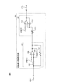
- FIG. 6 is a diagram showing the configuration of the low temperature side primary adjustment circuit.
- the low temperature side primary adjustment circuit 51 includes a first circuit 91 and a second circuit 92.
- the first circuit 91 is a circuit that changes the polarity (upward or downward) of the voltage VS1.
- the first circuit 91 includes a switch element 101, a resistor 102, an operational amplifier 103, and a resistor 104.
- the switch element 101 is controlled to be in the ON state when it is not necessary to change the polarity of the voltage VS1, and the voltage VS1 is output to the second circuit 92 as it is.
- the switch element 101 is controlled to an off state when it is necessary to change the polarity of the voltage VS1.
- the voltage VS1 is input to one end of the resistor 102.
- the other end of the resistor 102 is electrically connected to the inverting input terminal of the operational amplifier 103.
- the reference voltage VREF1 is input from the power supply circuit to the non-inverting input terminal of the operational amplifier 103.
- the operational amplifier 103 operates when the control signal ICL is at a high level, and does not operate when the control signal ICL is at a low level.
- One end of the resistor 104 is electrically connected to the inverting input terminal of the operational amplifier 103.
- the other end of the resistor 104 is electrically connected to the output terminal of the operational amplifier 103. That is, the resistor 102, the operational amplifier 103, and the resistor 104 form an inverting amplifier circuit.
- the inverting amplifier circuit changes the polarity of the voltage VS1.
- the low temperature side primary adjustment circuit 51 can adjust the inclination regardless of the polarity of the voltage VS1 (whether it rises to the right or falls to the right).
- the second circuit 92 includes a variable resistor 111, an operational amplifier 112, and a resistor 113.
- the output voltage of the first circuit 91 is input to one end of the variable resistor 111.
- the other end of the variable resistor 111 is electrically connected to the inverting input terminal of the operational amplifier 112.
- the reference voltage VREF2 is input from the power supply circuit to the non-inverting input terminal of the operational amplifier 112.
- the operational amplifier 112 operates when the control signal ICL is at a high level and does not operate when the control signal ICL is at a low level.
- One end of the resistor 113 is electrically connected to the inverting input terminal of the operational amplifier 112.
- the other end of the resistor 113 is electrically connected to the output terminal of the operational amplifier 112. That is, the second circuit 92 is an inverting amplifier circuit.
- the second circuit 92 outputs a voltage VTL obtained by multiplying the output voltage of the first circuit 91 by a gain to the low temperature side temperature compensation circuit 52.
- the gain of the second circuit 92 can be adjusted by adjusting the variable resistor 111. That is, the second circuit 92 can adjust the slope of the voltage VTL by adjusting the variable resistor 111. As a result, the second circuit 92 can match the slope of the voltage VTL with the slope of the primary component on the low temperature side of the model waveform 200.
- the low temperature side temperature compensation circuit 52 includes a primary compensation circuit 61, a tertiary compensation circuit 62, a fourth compensation circuit 63, and a fifth compensation circuit 64.
- the low temperature side temperature compensation circuit 52 has the voltage of the primary component output from the primary compensation circuit 61, the voltage of the tertiary component output from the tertiary compensation circuit 62, and the voltage of the tertiary component output from the fourth compensation circuit 63.
- the low temperature side compensation voltage VL is output by adding the voltage of the next component and the voltage of the fifth component output from the fifth compensation circuit 64.
- the low temperature side temperature compensation circuit 52 is not limited to this.
- the low temperature side temperature compensation circuit 52 may include at least a primary compensation circuit 61 and a tertiary compensation circuit 62.
- the low temperature side temperature compensation circuit 52 may include only the primary compensation circuit 61 and the tertiary compensation circuit 62.
- the low temperature side temperature compensation circuit 52 may include only the primary compensation circuit 61, the tertiary compensation circuit 62, and the fifth compensation circuit 64.
- the low temperature side temperature compensation circuit 52 may further include a compensation circuit of the sixth order or higher.
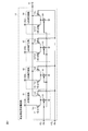
- FIG. 7 is a diagram showing the configuration of the low temperature side temperature compensation circuit.
- the primary compensation circuit 61 includes transistors Tr1 and Tr2 and a constant current source 121.
- the drain of the transistor Tr1 is electrically connected to the power supply potential VDD.
- a reference voltage V1 is input from the power supply circuit to the gate of the transistor Tr1.
- the source of the transistor Tr1 is electrically connected to the source of the transistor Tr2.
- a voltage VTL is input to the gate of the transistor Tr2 from the low temperature side primary adjustment circuit 51.
- the source of the transistor Tr2 is electrically connected to the source of the transistor Tr1.
- each transistor is a field effect transistor (FET), but the present disclosure is not limited to this.
- Each transistor may be a bipolar transistor. FETs are preferable from the viewpoint of cost, mounting area, and low power consumption. However, the FET has more phase noise than the bipolar transistor. Therefore, from the viewpoint of suppressing phase noise, a bipolar transistor is preferable.
- the constant current source 121 causes a constant current to flow between the source of the transistors Tr1 and Tr2 and the reference potential when the control signal ICL is at a high level.
- the constant current source 121 does not pass a current when the control signal ICL is at a low level.
- the primary compensation circuit 61 is a source-coupled amplifier circuit (emitter-coupled amplifier circuit).
- the tertiary compensation circuit 62 includes transistors Tr3 and Tr4 and a constant current source 122.
- the internal connection relationship of the tertiary compensation circuit 62 is the same as the internal connection relationship of the primary compensation circuit 61. That is, the tertiary compensation circuit 62 is a source coupling amplifier circuit.
- the reference voltage V2 is input from the power supply circuit to the gate of the transistor Tr3.
- a voltage VTL is input to the gate of the transistor Tr4 from the low temperature side primary adjustment circuit 51.
- the constant current source 122 causes a constant current to flow between the source of the transistors Tr3 and Tr4 and the reference potential when the control signal ICL is at a high level.
- the constant current source 122 does not carry current when the control signal ICL is at a low level.
- the fourth-order compensation circuit 63 includes transistors Tr5 and Tr6, and a constant current source 123.
- the internal connection relationship of the fourth compensation circuit 63 is the same as the internal connection relationship of the primary compensation circuit 61. That is, the fourth-order compensation circuit 63 is a source coupling amplifier circuit.
- the reference voltage V3 is input from the power supply circuit to the gate of the transistor Tr5.
- a voltage VTL is input to the gate of the transistor Tr6 from the low temperature side primary adjustment circuit 51.
- the constant current source 123 causes a constant current to flow between the source of the transistors Tr5 and Tr6 and the reference potential when the control signal ICL is at a high level.
- the constant current source 123 does not carry current when the control signal ICL is at a low level.
- the fifth-order compensation circuit 64 includes transistors Tr7 and Tr8 and a constant current source 124.
- the internal connection relationship of the fifth-order compensation circuit 64 is the same as the internal connection relationship of the primary compensation circuit 61. That is, the fifth-order compensation circuit 64 is a source coupling amplifier circuit.
- the reference voltage V4 is input from the power supply circuit to the gate of the transistor Tr7.
- a voltage VTL is input to the gate of the transistor Tr8 from the low temperature side primary adjustment circuit 51.
- the constant current source 124 causes a constant current to flow between the source of the transistors Tr7 and Tr8 and the reference potential when the control signal ICL is at a high level.
- the constant current source 124 does not carry current when the control signal ICL is low level.
- the drains of the transistors Tr2, Tr4, Tr6 and Tr8 are connected by wiring and output the low temperature side compensation voltage VL.
- the low temperature side compensation voltage VL corresponds to the "low temperature side compensation signal" of the present disclosure.
- the high temperature side primary adjustment circuit 53 adjusts the inclination of the primary component of the high temperature side compensation voltage VH when the control signal ICH is at a high level.
- the high temperature side primary adjustment circuit 53 does not operate when the control signal ICH is at a low level. Since the configuration of the high temperature side primary adjustment circuit 53 is the same as the configuration of the low temperature side primary adjustment circuit 51 (see FIG. 6), illustration and description thereof will be omitted.
- the high temperature side temperature compensation circuit 54 includes a primary compensation circuit 71, a tertiary compensation circuit 72, a fourth compensation circuit 73, and a fifth compensation circuit 74. Since the configuration of the high temperature side temperature compensation circuit 54 is the same as that of the low temperature side temperature compensation circuit 52 (see FIG. 7), illustration and description thereof will be omitted.
- the low temperature side temperature compensation circuit 52 has the voltage of the primary component output from the primary compensation circuit 71, the voltage of the tertiary component output from the tertiary compensation circuit 72, and the voltage of the tertiary component output from the fourth compensation circuit 73.
- the high temperature side compensation voltage VH is output by adding the voltage of the next component and the voltage of the fifth component output from the fifth compensation circuit 74.
- the high temperature side compensation voltage VH corresponds to the "high temperature side compensation signal" of the present disclosure.
- the output terminal of the low temperature side temperature compensation circuit 52 and the output terminal of the high temperature side temperature compensation circuit 54 are connected by wiring, and the compensation voltage VSUM is output to the adjustment circuit 34.
- the adjusting circuit 34 includes a 0th order adjusting circuit 81, a 3rd order adjusting circuit 82, a 4th order adjusting circuit 83, and a 5th order adjusting circuit 84.
- the compensation voltage VSUM is input to the 0th adjustment circuit 81, the 3rd adjustment circuit 82, the 4th adjustment circuit 83, and the 5th adjustment circuit 84.
- the adjustment circuit 34 is not limited to this.
- the adjustment circuit 34 may correspond to the configuration of the low temperature side temperature compensation circuit 52 (and the high temperature side temperature compensation circuit 54). For example, when the low temperature side temperature compensation circuit 52 does not include the fourth compensation circuit 63, the adjustment circuit 34 may not include the fourth adjustment circuit 83. Further, for example, when the low temperature side temperature compensation circuit 52 does not include the fifth-order compensation circuit 64, the adjustment circuit 34 may not include the fifth-order adjustment circuit 84. Further, for example, when the low temperature side temperature compensation circuit 52 further includes a compensation circuit of 6th order or higher, the adjustment circuit 34 may further include an adjustment circuit of 6th order or higher.
- the adjustment circuit 34 adjusts components of orders other than the first order of the compensation voltage VSUM (compensation voltage VL on the low temperature side and compensation voltage VH on the high temperature side). It is exemplified that the 0th-order adjustment circuit 81 adjusts the 0th-order component (DC component, bias) of the compensation voltage VSUM. It is exemplified that the third-order adjustment circuit 82 adjusts the amplitude of the third-order component of the compensation voltage VSUM. It is exemplified that the fourth-order adjustment circuit 83 adjusts the slope of the fourth-order component of the compensation voltage VSUM. It is exemplified that the fifth-order adjustment circuit 84 adjusts the slope of the fifth-order component of the compensation voltage VSUM.
- the output terminal of the 0th adjustment circuit 81, the output terminal of the 3rd adjustment circuit 82, the output terminal of the 4th adjustment circuit 83, and the output terminal of the 5th adjustment circuit 84 are connected by wiring, and the control voltage VCTR is set to VCXO2. Output to.
- FIG. 8 is a diagram for explaining the operation of the temperature compensation circuit in a simplified manner.
- the first temperature detection circuit 3-1 outputs a voltage VS1 having a linear waveform having a polarity (downward to the right) whose voltage decreases as the temperature rises to the low temperature side primary adjustment circuit 51.
- the low temperature side primary adjustment circuit 51 outputs the voltage VTL adjusted so that the slope of the voltage VS1 is indicated by the arrow 210 to the low temperature side temperature compensation circuit 52.
- the low temperature side temperature compensation circuit 52 and the adjustment circuit 34 output the control voltage VCTR to the VCXO2 based on the voltage VTL.
- the slope of the primary component of the control voltage VCTR is adjusted as shown by the arrow 212.
- the second temperature detection circuit 3-2 outputs a voltage VS2 having a linear waveform having a polarity (downward to the right) whose voltage decreases as the temperature rises to the high temperature side primary adjustment circuit 53.
- the high temperature side primary adjustment circuit 53 outputs the voltage VTH adjusted by adjusting the slope of the voltage VS2 as indicated by the arrow 211 to the high temperature side temperature compensation circuit 54.
- the high temperature side temperature compensation circuit 54 and the adjustment circuit 34 output the control voltage VCTR to the VCXO2 based on the voltage VTH.
- the slope of the primary component of the control voltage VCTR is adjusted as shown by the arrow 213.
- the temperature compensation circuit 4 can separately adjust the inclination of the primary component of the control voltage VCTR on the low temperature side and the inclination of the primary component of the control voltage VCTR on the high temperature side.
- the low temperature side primary adjustment circuit 51 can suppress the correction error of the low temperature side primary component
- the high temperature side primary adjustment circuit 53 suppresses the correction error of the high temperature side primary component. it can. Therefore, the temperature compensation circuit 4 can suppress the correction error of the primary component in the entire operating temperature range.
- FIG. 9 is a diagram showing the configuration of the temperature compensated crystal oscillator (TCXO) of the second embodiment.
- the first temperature detection circuit 3-1 outputs the voltage VS1 to the low temperature side primary adjustment circuit 51, and the second temperature detection circuit 3-2 outputs the voltage VS2 to the high temperature side 1 It was output to the next adjustment circuit 53.
- the first temperature detection circuit 3-1 outputs the voltage VS1 to the low temperature side primary adjustment circuit 51 and the high temperature side primary adjustment circuit 53. Therefore, TCXO1A does not include the second temperature detection circuit 3-2.
- the TCXO1A can reduce the number of parts, the mounting area, and the manufacturing cost.
Landscapes
- Oscillators With Electromechanical Resonators (AREA)
Priority Applications (1)
| Application Number | Priority Date | Filing Date | Title |
|---|---|---|---|
| JP2021532668A JPWO2021009956A1 (https=) | 2019-07-17 | 2020-02-17 |
Applications Claiming Priority (2)
| Application Number | Priority Date | Filing Date | Title |
|---|---|---|---|
| JP2019131974 | 2019-07-17 | ||
| JP2019-131974 | 2019-07-17 |
Publications (1)
| Publication Number | Publication Date |
|---|---|
| WO2021009956A1 true WO2021009956A1 (ja) | 2021-01-21 |
Family
ID=74210530
Family Applications (1)
| Application Number | Title | Priority Date | Filing Date |
|---|---|---|---|
| PCT/JP2020/006087 Ceased WO2021009956A1 (ja) | 2019-07-17 | 2020-02-17 | 温度補償回路及び温度補償水晶発振器 |
Country Status (2)
| Country | Link |
|---|---|
| JP (1) | JPWO2021009956A1 (https=) |
| WO (1) | WO2021009956A1 (https=) |
Cited By (3)
| Publication number | Priority date | Publication date | Assignee | Title |
|---|---|---|---|---|
| JP2023125261A (ja) * | 2022-02-28 | 2023-09-07 | セイコーエプソン株式会社 | 回路装置及び発振器 |
| US12126294B2 (en) | 2022-11-29 | 2024-10-22 | Alpha And Omega Semiconductor International Lp | Post measurement calibrating translation circuit |
| US12394964B2 (en) | 2023-01-30 | 2025-08-19 | Banner Engineering Corp. | Self-fitting pressure equalizing waterproof electronics enclosure |
Citations (3)
| Publication number | Priority date | Publication date | Assignee | Title |
|---|---|---|---|---|
| JP2004172877A (ja) * | 2002-11-19 | 2004-06-17 | Nippon Dempa Kogyo Co Ltd | 非線形関数発生回路及びこれを用いた温度補償発振器 |
| JP2006253974A (ja) * | 2005-03-09 | 2006-09-21 | Epson Toyocom Corp | 温度補償型圧電発振器 |
| JP2017212637A (ja) * | 2016-05-26 | 2017-11-30 | 旭化成エレクトロニクス株式会社 | 調整装置、調整方法、および発振装置 |
-
2020
- 2020-02-17 JP JP2021532668A patent/JPWO2021009956A1/ja active Pending
- 2020-02-17 WO PCT/JP2020/006087 patent/WO2021009956A1/ja not_active Ceased
Patent Citations (3)
| Publication number | Priority date | Publication date | Assignee | Title |
|---|---|---|---|---|
| JP2004172877A (ja) * | 2002-11-19 | 2004-06-17 | Nippon Dempa Kogyo Co Ltd | 非線形関数発生回路及びこれを用いた温度補償発振器 |
| JP2006253974A (ja) * | 2005-03-09 | 2006-09-21 | Epson Toyocom Corp | 温度補償型圧電発振器 |
| JP2017212637A (ja) * | 2016-05-26 | 2017-11-30 | 旭化成エレクトロニクス株式会社 | 調整装置、調整方法、および発振装置 |
Cited By (5)
| Publication number | Priority date | Publication date | Assignee | Title |
|---|---|---|---|---|
| JP2023125261A (ja) * | 2022-02-28 | 2023-09-07 | セイコーエプソン株式会社 | 回路装置及び発振器 |
| US12244268B2 (en) | 2022-02-28 | 2025-03-04 | Seiko Epson Corporation | Circuit device and oscillator |
| JP7815851B2 (ja) | 2022-02-28 | 2026-02-18 | セイコーエプソン株式会社 | 回路装置及び発振器 |
| US12126294B2 (en) | 2022-11-29 | 2024-10-22 | Alpha And Omega Semiconductor International Lp | Post measurement calibrating translation circuit |
| US12394964B2 (en) | 2023-01-30 | 2025-08-19 | Banner Engineering Corp. | Self-fitting pressure equalizing waterproof electronics enclosure |
Also Published As
| Publication number | Publication date |
|---|---|
| JPWO2021009956A1 (https=) | 2021-01-21 |
Similar Documents
| Publication | Publication Date | Title |
|---|---|---|
| US7852164B2 (en) | Piezoelectric oscillator | |
| US20140327486A1 (en) | RC Oscillator | |
| US8659361B2 (en) | Function generator circuit | |
| KR100324002B1 (ko) | 안정화발진회로 | |
| JP2010130141A (ja) | 電圧制御型温度補償圧電発振器 | |
| JP5129394B2 (ja) | 発振器 | |
| WO2021009956A1 (ja) | 温度補償回路及び温度補償水晶発振器 | |
| US7348859B2 (en) | Crystal oscillator | |
| US11356057B2 (en) | Temperature control circuit, oscillation control circuit, and temperature control method | |
| Ates et al. | Fully integrated frequency reference with 1.7 ppm temperature accuracy within 0–80° C | |
| JP6377192B2 (ja) | 温度補償型水晶発振器 | |
| US11018625B1 (en) | Frequency reference generator | |
| US11211898B2 (en) | Oscillator circuits | |
| JP5034772B2 (ja) | 温度補償圧電発振器 | |
| JP2007318397A (ja) | 電圧制御型発振器及びその周波数制御方法 | |
| US8610513B2 (en) | Crystal oscillator | |
| JP4428124B2 (ja) | 温度補償発振器 | |
| JP2002135051A (ja) | 圧電発振器 | |
| JP4311313B2 (ja) | 圧電発振器 | |
| JP2001060828A (ja) | 温度補償発振器 | |
| WO2020067341A1 (ja) | 温度補償回路及び温度補償水晶発振器 | |
| WO2020066672A1 (ja) | 温度補償回路及び温度補償水晶発振器 | |
| WO2023234141A1 (ja) | 温度補償型圧電発振器 | |
| JP5918546B2 (ja) | 温度補償型水晶発振器 | |
| JP4314988B2 (ja) | 温度補償型圧電発振器 |
Legal Events
| Date | Code | Title | Description |
|---|---|---|---|
| 121 | Ep: the epo has been informed by wipo that ep was designated in this application |
Ref document number: 20841370 Country of ref document: EP Kind code of ref document: A1 |
|
| ENP | Entry into the national phase |
Ref document number: 2021532668 Country of ref document: JP Kind code of ref document: A |
|
| NENP | Non-entry into the national phase |
Ref country code: DE |
|
| 122 | Ep: pct application non-entry in european phase |
Ref document number: 20841370 Country of ref document: EP Kind code of ref document: A1 |