WO2021002225A1 - 半導体装置 - Google Patents
半導体装置 Download PDFInfo
- Publication number
- WO2021002225A1 WO2021002225A1 PCT/JP2020/024238 JP2020024238W WO2021002225A1 WO 2021002225 A1 WO2021002225 A1 WO 2021002225A1 JP 2020024238 W JP2020024238 W JP 2020024238W WO 2021002225 A1 WO2021002225 A1 WO 2021002225A1
- Authority
- WO
- WIPO (PCT)
- Prior art keywords
- lead
- semiconductor device
- back surface
- resin
- terminal
- Prior art date
- Legal status (The legal status is an assumption and is not a legal conclusion. Google has not performed a legal analysis and makes no representation as to the accuracy of the status listed.)
- Ceased
Links
Images







Classifications
-
- H—ELECTRICITY
- H10—SEMICONDUCTOR DEVICES; ELECTRIC SOLID-STATE DEVICES NOT OTHERWISE PROVIDED FOR
- H10D—INORGANIC ELECTRIC SEMICONDUCTOR DEVICES
- H10D64/00—Electrodes of devices having potential barriers
- H10D64/20—Electrodes characterised by their shapes, relative sizes or dispositions
- H10D64/23—Electrodes carrying the current to be rectified, amplified, oscillated or switched, e.g. sources, drains, anodes or cathodes
- H10D64/251—Source or drain electrodes for field-effect devices
- H10D64/254—Source or drain electrodes for field-effect devices for lateral devices wherein the source or drain electrodes extend entirely through the semiconductor bodies, e.g. via-holes for back side contacts
-
- H—ELECTRICITY
- H10—SEMICONDUCTOR DEVICES; ELECTRIC SOLID-STATE DEVICES NOT OTHERWISE PROVIDED FOR
- H10W—GENERIC PACKAGES, INTERCONNECTIONS, CONNECTORS OR OTHER CONSTRUCTIONAL DETAILS OF DEVICES COVERED BY CLASS H10
- H10W20/00—Interconnections in chips, wafers or substrates
- H10W20/40—Interconnections external to wafers or substrates, e.g. back-end-of-line [BEOL] metallisations or vias connecting to gate electrodes
- H10W20/482—Interconnections external to wafers or substrates, e.g. back-end-of-line [BEOL] metallisations or vias connecting to gate electrodes for individual devices provided for in groups H10D8/00 - H10D48/00, e.g. for power transistors
- H10W20/484—Interconnections having extended contours, e.g. pads having mesh shape or interconnections comprising connected parallel stripes
-
- H—ELECTRICITY
- H10—SEMICONDUCTOR DEVICES; ELECTRIC SOLID-STATE DEVICES NOT OTHERWISE PROVIDED FOR
- H10W—GENERIC PACKAGES, INTERCONNECTIONS, CONNECTORS OR OTHER CONSTRUCTIONAL DETAILS OF DEVICES COVERED BY CLASS H10
- H10W70/00—Package substrates; Interposers; Redistribution layers [RDL]
- H10W70/40—Leadframes
- H10W70/481—Leadframes for devices being provided for in groups H10D8/00 - H10D48/00
-
- H—ELECTRICITY
- H10—SEMICONDUCTOR DEVICES; ELECTRIC SOLID-STATE DEVICES NOT OTHERWISE PROVIDED FOR
- H10W—GENERIC PACKAGES, INTERCONNECTIONS, CONNECTORS OR OTHER CONSTRUCTIONAL DETAILS OF DEVICES COVERED BY CLASS H10
- H10W72/00—Interconnections or connectors in packages
-
- H—ELECTRICITY
- H10—SEMICONDUCTOR DEVICES; ELECTRIC SOLID-STATE DEVICES NOT OTHERWISE PROVIDED FOR
- H10W—GENERIC PACKAGES, INTERCONNECTIONS, CONNECTORS OR OTHER CONSTRUCTIONAL DETAILS OF DEVICES COVERED BY CLASS H10
- H10W74/00—Encapsulations, e.g. protective coatings
- H10W74/10—Encapsulations, e.g. protective coatings characterised by their shape or disposition
- H10W74/111—Encapsulations, e.g. protective coatings characterised by their shape or disposition the semiconductor body being completely enclosed
-
- H—ELECTRICITY
- H10—SEMICONDUCTOR DEVICES; ELECTRIC SOLID-STATE DEVICES NOT OTHERWISE PROVIDED FOR
- H10W—GENERIC PACKAGES, INTERCONNECTIONS, CONNECTORS OR OTHER CONSTRUCTIONAL DETAILS OF DEVICES COVERED BY CLASS H10
- H10W74/00—Encapsulations, e.g. protective coatings
- H10W74/40—Encapsulations, e.g. protective coatings characterised by their materials
- H10W74/47—Encapsulations, e.g. protective coatings characterised by their materials comprising organic materials, e.g. plastics or resins
-
- H—ELECTRICITY
- H10—SEMICONDUCTOR DEVICES; ELECTRIC SOLID-STATE DEVICES NOT OTHERWISE PROVIDED FOR
- H10D—INORGANIC ELECTRIC SEMICONDUCTOR DEVICES
- H10D30/00—Field-effect transistors [FET]
- H10D30/40—FETs having zero-dimensional [0D], one-dimensional [1D] or two-dimensional [2D] charge carrier gas channels
- H10D30/47—FETs having zero-dimensional [0D], one-dimensional [1D] or two-dimensional [2D] charge carrier gas channels having two-dimensional [2D] charge carrier gas channels, e.g. nanoribbon FETs or high electron mobility transistors [HEMT]
- H10D30/471—High electron mobility transistors [HEMT] or high hole mobility transistors [HHMT]
- H10D30/475—High electron mobility transistors [HEMT] or high hole mobility transistors [HHMT] having wider bandgap layer formed on top of lower bandgap active layer, e.g. undoped barrier HEMTs such as i-AlGaN/GaN HEMTs
-
- H—ELECTRICITY
- H10—SEMICONDUCTOR DEVICES; ELECTRIC SOLID-STATE DEVICES NOT OTHERWISE PROVIDED FOR
- H10D—INORGANIC ELECTRIC SEMICONDUCTOR DEVICES
- H10D62/00—Semiconductor bodies, or regions thereof, of devices having potential barriers
- H10D62/10—Shapes, relative sizes or dispositions of the regions of the semiconductor bodies; Shapes of the semiconductor bodies
- H10D62/17—Semiconductor regions connected to electrodes not carrying current to be rectified, amplified or switched, e.g. channel regions
- H10D62/343—Gate regions of field-effect devices having PN junction gates
-
- H—ELECTRICITY
- H10—SEMICONDUCTOR DEVICES; ELECTRIC SOLID-STATE DEVICES NOT OTHERWISE PROVIDED FOR
- H10D—INORGANIC ELECTRIC SEMICONDUCTOR DEVICES
- H10D62/00—Semiconductor bodies, or regions thereof, of devices having potential barriers
- H10D62/80—Semiconductor bodies, or regions thereof, of devices having potential barriers characterised by the materials
- H10D62/85—Semiconductor bodies, or regions thereof, of devices having potential barriers characterised by the materials being Group III-V materials, e.g. GaAs
- H10D62/8503—Nitride Group III-V materials, e.g. AlN or GaN
-
- H—ELECTRICITY
- H10—SEMICONDUCTOR DEVICES; ELECTRIC SOLID-STATE DEVICES NOT OTHERWISE PROVIDED FOR
- H10D—INORGANIC ELECTRIC SEMICONDUCTOR DEVICES
- H10D64/00—Electrodes of devices having potential barriers
- H10D64/111—Field plates
-
- H—ELECTRICITY
- H10—SEMICONDUCTOR DEVICES; ELECTRIC SOLID-STATE DEVICES NOT OTHERWISE PROVIDED FOR
- H10D—INORGANIC ELECTRIC SEMICONDUCTOR DEVICES
- H10D64/00—Electrodes of devices having potential barriers
- H10D64/20—Electrodes characterised by their shapes, relative sizes or dispositions
- H10D64/23—Electrodes carrying the current to be rectified, amplified, oscillated or switched, e.g. sources, drains, anodes or cathodes
- H10D64/251—Source or drain electrodes for field-effect devices
- H10D64/257—Source or drain electrodes for field-effect devices for lateral devices wherein the source or drain electrodes are characterised by top-view geometrical layouts, e.g. interdigitated, semi-circular, annular or L-shaped electrodes
Definitions
- This disclosure relates to semiconductor devices.
- a semiconductor device that is a HEMT (High Electron Mobility Transistor) using a Group III-V nitride semiconductor (hereinafter, may be referred to as "nitride semiconductor") such as gallium nitride (GaN).
- nitride semiconductor Group III-V nitride semiconductor
- GaN gallium nitride
- a semiconductor element is mounted, a source lead conducting to the source electrode, a drain lead conducting to the drain electrode, a gate lead conducting to the gate electrode, and a sealing resin covering the semiconductor element and each lead. It has. A part of each lead is exposed from the sealing resin and serves as a terminal for mounting on a circuit board.
- the main current to be switched is input from the drain lead and flows to the drain electrode, flows in the HEMT from the drain electrode to the source electrode, and flows from the source electrode to the source lead and is output. ..
- the inductance increases with the length of this current path. The inductance may affect the switching performance of the semiconductor device.
- one object of the present disclosure is to provide a semiconductor device capable of reducing inductance.
- the semiconductor device provided by the present disclosure includes an electron traveling layer made of a nitride semiconductor, an element main surface and an element back surface facing opposite sides in the thickness direction, and a gate electrode and a source electrode arranged on the element main surface. , And a semiconductor element having a drain electrode, a first lead to which the drain electrode is bonded, a second lead to which the source electrode is bonded, and the element connected to the second lead.
- a connection lead arranged so as to overlap the semiconductor element in the thickness direction is provided on the back surface side, and a main current to be switched flows through the connection lead.
- the main current is input from the first lead and flows to the drain electrode, flows in the semiconductor element from the drain electrode to the source electrode, flows from the source electrode to the second lead, and flows from the second lead to the connecting lead. .. Since the drain electrode is bonded to the first lead and the source electrode is bonded to the second lead, the inductance is reduced as compared with the case where the drain electrode is bonded by a bonding wire. Further, the connection leads are arranged on the back surface side of the element so as to overlap the semiconductor element, and the main current flows in the direction opposite to the current path from the first lead to the second lead. Since the magnetic field generated by the main current flowing in the current path from the first lead to the second lead cancels out the magnetic field generated by the main current flowing in the connecting lead, the generated inductance is reduced.
- FIG. It is a perspective view which shows the semiconductor device which concerns on 1st Embodiment. It is a top view of the semiconductor device shown in FIG. It is a top view of the semiconductor device shown in FIG. It is a front view of the semiconductor device shown in FIG. It is a bottom view of the semiconductor device shown in FIG. It is a right side view of the semiconductor device shown in FIG. It is sectional drawing which follows the line VII-VII of FIG. It is a top view which shows the semiconductor element. It is a schematic cross-sectional view which shows the semiconductor element. It is sectional drawing which shows the semiconductor device which concerns on 2nd Embodiment. It is sectional drawing which shows the semiconductor device which concerns on 3rd Embodiment.
- the semiconductor device A1 according to the first embodiment of the present disclosure will be described with reference to FIGS. 1 to 9.
- the semiconductor device A1 includes a plurality of leads 1 to 5, a connection lead 6, a semiconductor element 7, and a sealing resin 8.
- FIG. 1 is a perspective view showing the semiconductor device A1.
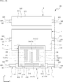
- 2 and 3 are plan views showing the semiconductor device A1.
- the outer shape of the sealing resin 8 is shown by an imaginary line (dashed line) through the sealing resin 8 and the connecting lead 6.
- the semiconductor element 7 is further transmitted.
- FIG. 4 is a front view showing the semiconductor device A1.
- FIG. 5 is a bottom view showing the semiconductor device A1.
- FIG. 6 is a right side view showing the semiconductor device A1.
- FIG. 7 is a cross-sectional view taken along the line VII-VII of FIG.
- FIG. 8 is a plan view showing the semiconductor element 7.
- FIG. 9 is a schematic cross-sectional view showing the semiconductor element 7.
- the semiconductor device A1 shown in these figures is a device that is surface-mounted on the circuit boards of various devices.
- the shape of the semiconductor device A1 in the thickness direction is rectangular.
- the thickness direction of the semiconductor device A1 is the z direction, and the directions along one side of the semiconductor device A1 orthogonal to the z direction (the left-right direction in FIG. 2) are orthogonal to the x direction, the z direction, and the x direction.
- the direction (vertical direction in FIG. 2) is the y direction.
- the z direction corresponds to the "thickness direction" of the present disclosure.
- the size of the semiconductor device A1 is not particularly limited, and in the present embodiment, for example, the x-direction dimension is about 1 to 10 mm, the y-direction dimension is about 1 to 20 mm, and the z-direction dimension is about 0.3 to 3 mm.
- the plurality of leads 1 to 5 support the semiconductor element 7 and are electrically connected to the semiconductor element 7.
- Leads 1-5 are made of metal, preferably either Cu or Ni, or alloys thereof, 42 alloys, and the like. In this embodiment, the case where the leads 1 to 5 are made of Cu will be described as an example.
- the thickness of the leads 1 to 5 is, for example, 0.08 to 1 mm, and in the present embodiment, it is about 0.5 mm.
- the leads 1 to 5 are formed by, for example, etching a metal plate.
- the leads 1 to 5 may be formed by punching, bending, or the like on a metal plate. In the following description, when the leads 1 to 5 are described individually, they are described as the first lead 1, the second lead 2, the third lead 3, the fourth lead 4, and the fifth lead 5. When they are collectively shown, they are described as leads 1 to 5.
- the first lead 1 is arranged substantially in the center of the semiconductor device A1 in the y direction and extends in the entire x direction.
- the second lead 2 and the third lead 3 are arranged on opposite sides of the first lead 1 in the y direction, respectively, apart from the first lead 1.
- the second lead 2 is an end portion on one side (lower side in FIG. 3) in the y direction, and is arranged substantially at the center in the x direction.
- the third lead 3 is arranged at the end on the other side in the y direction (upper side in FIG. 3) and extends in the entire x direction.
- the fourth lead 4 and the fifth lead 5 are arranged on the same side as the second lead 2 (lower side in FIG.
- the third lead 3, the second lead 2, the fourth lead 4, and the fifth lead 5 are arranged on opposite sides of the first lead 1. Further, the fourth lead 4 and the fifth lead 5 are arranged on opposite sides of the second lead 2 in the x direction, respectively, separated from the second lead 2.
- the fourth lead 4 is an end portion on one side in the y direction and is arranged at an end portion on one side (left side in FIG. 3) in the x direction.
- the fifth lead 5 is an end portion on one side in the y direction and is arranged at the end portion on the other side (right side in FIG. 3) in the x direction.
- the first lead 1 has a larger z-direction visual dimension than the other leads 2 to 5. The z-direction visual dimension becomes smaller in the order of the third lead 3 and the second lead 2, and the fourth lead 4 and the fifth lead 5 are the same and the smallest.
- the first lead 1 includes a terminal portion 110, a connecting portion 120, and an extending portion 130.
- the terminal portion 110 has a rectangular shape that is long in the x direction when viewed in the z direction.
- the terminal portion 110 has a terminal portion main surface 111 and a terminal portion back surface 112.
- the terminal main surface 111 and the terminal back surface 112 face opposite to each other in the z direction.
- the terminal portion main surface 111 is a surface facing upward in FIGS. 4, 6 and 7.
- the terminal portion main surface 111 is a surface to which a part of the semiconductor element 7 is joined.
- the back surface 112 of the terminal portion is a surface facing downward in FIGS. 4, 6 and 7.
- the back surface 112 of the terminal portion is exposed from the sealing resin 8 and becomes a back surface terminal.
- the terminal portion 110 may be formed by, for example, half-etching a recess on the back surface side in which a part of the terminal portion 110 is recessed from the back surface 112 of the terminal portion in the z direction.
- the connecting portion 120 is connected to the terminal portion 110 and has a rectangular shape in the z direction.
- One connecting portion 120 is arranged on one end surface of the terminal portion 110 in the x direction. Further, one connecting portion 120 is also arranged on the other end face of the terminal portion 110 in the x direction. That is, a total of two connecting portions 120 are arranged.
- Each connecting portion 120 has a connecting portion main surface 121, a connecting portion back surface 122, and a connecting portion end surface 123.
- the main surface 121 of the connecting portion and the back surface 122 of the connecting portion face each other in the z direction.
- the main surface 121 of the connecting portion is a surface facing upward in FIGS. 4, 6 and 7.
- the main surface 121 of the connecting portion and the main surface 111 of the terminal portion are flush with each other.
- the back surface 122 of the connecting portion is a surface facing downward in FIGS. 4, 6 and 7.
- the thickness of the connecting portion 120 (dimension in the z direction) is about half the thickness of the terminal portion 110.
- the connecting portion 120 is formed by, for example, a half etching process.
- the connecting portion end surface 123 is a surface connecting the connecting portion main surface 121 and the connecting portion back surface 122, and faces outward in the x direction. The end face 123 of the connecting portion is exposed from the sealing resin 8 (see FIGS. 1 and 6).
- the extending portion 130 is connected to the terminal portion 110 and has a rectangular shape that is long in the y direction in the z direction.
- the extending portion 130 extends in the y direction from one end surface (lower end surface in FIG. 3) of the terminal portion 110 in the y direction. That is, the extending portion 130 extends from the terminal portion 110 toward the second lead 2 side.
- three extension portions 130 are arranged side by side at equal intervals in the x direction. That is, the first lead 1 is formed in a comb-teeth shape as a whole in the z-direction view.
- Each extension portion 130 has an extension portion main surface 131 and an extension portion back surface 132.
- the extension portion main surface 131 and the extension portion back surface 132 face opposite to each other in the z direction.
- the extension portion main surface 131 is a surface facing upward in FIGS. 4, 6 and 7.
- the extension portion main surface 131 is a surface to which a part of the semiconductor element 7 is joined.
- the main surface 131 of the extension portion and the main surface 111 of the terminal portion are flush with each other. Therefore, the terminal portion main surface 111, the connecting portion main surface 121, and the extending portion main surface 131 are flush with each other (see FIG. 3).
- the back surface 132 of the extending portion is a surface facing downward in FIGS. 4, 6 and 7.
- the thickness (dimension in the z direction) of the extending portion 130 is about half the thickness of the terminal portion 110.
- the extending portion 130 is formed by, for example, a half etching process.
- the extending portion 130 is entirely covered with the sealing resin 8 and is not exposed from the sealing resin 8.
- the extension unit 130 corresponds to the “first extension
- the second lead 2 includes a support portion 210 and an extension portion 230.
- the support portion 210 has a rectangular shape that is long in the x direction when viewed in the z direction.
- the support portion 210 has a support portion main surface 211, a support portion back surface 212, and a support portion end surface 213.
- the support portion main surface 211 and the support portion back surface 212 face each other in the z direction.
- the support portion main surface 211 is a surface facing upward in FIGS. 4, 6 and 7.
- the main surface 211 of the support portion is a surface to which a part of the semiconductor element 7 is joined.
- the back surface 212 of the support portion is a surface facing downward in FIGS. 4, 6 and 7.
- the thickness of the support portion 210 (dimension in the z direction) is about half the thickness of the terminal portion 110 of the first lead 1.
- the support portion 210 is formed by, for example, a half-etching process.
- the main surface 211 of the support portion and the back surface 212 of the support portion are not exposed from the sealing resin 8.
- the support portion end surface 213 is a surface connecting the support portion main surface 211 and the support portion back surface 212, and faces the outer side in the y direction (lower side in FIG. 3).
- the end face 213 of the support portion is exposed from the sealing resin 8 (see FIGS. 1 and 4).
- the extending portion 230 is connected to the supporting portion 210 and has a rectangular shape that is long in the y direction in the z direction.
- the extending portion 230 extends in the y direction from the other end surface (upper end surface in FIG. 3) of the supporting portion 210 in the y direction. That is, the extending portion 230 extends from the supporting portion 210 toward the first lead 1 side.
- two extension portions 230 are arranged side by side in the x direction. That is, the second lead 2 is formed in a comb-teeth shape as a whole in the z-direction view. Further, each extension portion 230 is arranged between the extension portions 130 of the first lead 1.
- each extension portion 230 has an extension portion main surface 231 and an extension portion back surface 232.
- the main surface of the extension portion 231 and the back surface of the extension portion 232 face each other in the z direction.
- the extension portion main surface 231 is a surface facing upward in FIGS. 4, 6 and 7.
- the extension portion main surface 231 is a surface to which a part of the semiconductor element 7 is joined.
- the main surface 231 of the extending portion and the main surface 211 of the supporting portion are flush with each other.
- the back surface 232 of the extension portion is a surface facing downward in FIGS. 4, 6 and 7.
- the back surface 232 of the extension portion and the back surface 212 of the support portion are flush with each other. That is, the thickness of the extending portion 230 (dimension in the z direction) is about the same as the thickness of the supporting portion 210.
- the extending portion 230 is formed by, for example, a half etching process.
- the extending portion 230 is entirely covered with the sealing resin 8 and is not exposed from the sealing resin 8.
- the extension section 230 corresponds to the “second extension section” of the present disclosure.
- the third reed 3 includes a terminal portion 310 and a connecting portion 320.
- the terminal portion 310 has a rectangular shape that is long in the x direction when viewed in the z direction.
- the terminal portion 310 has a terminal portion main surface 311 and a terminal portion back surface 312, and a terminal portion end surface 313.
- the terminal main surface 311 and the terminal back surface 312 face opposite to each other in the z direction.
- the terminal portion main surface 311 is a surface facing upward in FIGS. 4, 6 and 7.
- the terminal portion main surface 311 is a surface to which a part of the semiconductor element 7 is joined.
- the terminal back surface 312 is a surface facing downward in FIGS. 4, 6 and 7.
- the back surface 312 of the terminal portion is exposed from the sealing resin 8 and becomes a back surface terminal.
- the thickness of the terminal portion 310 (dimension in the z direction) is about the same as the thickness of the terminal portion 110 of the first lead 1.
- the terminal portion 310 may be formed by, for example, half-etching a back surface side recess in which a part of the terminal portion 310 is recessed from the terminal portion back surface 312 in the z direction.
- the terminal end surface 313 is a surface connecting the terminal main surface 311 and the terminal back surface 312, and faces the outside in the y direction (upper side in FIG. 3), that is, the side opposite to the first lead 1.
- the terminal end surface 313 is exposed from the sealing resin 8 and becomes a terminal.
- the terminal end face 313 corresponds to the "third end face" of the present disclosure.
- the connecting portion 320 is connected to the terminal portion 310 and has a rectangular shape in the z direction.
- One connecting portion 320 is arranged on one end surface of the terminal portion 310 in the x direction. Further, one connecting portion 320 is also arranged on the other end face of the terminal portion 310 in the x direction. That is, a total of two connecting portions 320 are arranged.
- Each connecting portion 320 has a connecting portion main surface 321 and a connecting portion back surface 322, and a connecting portion end surface 323.
- the main surface 321 of the connecting portion and the back surface 322 of the connecting portion face each other in the z direction.
- the main surface 321 of the connecting portion is a surface facing upward in FIGS. 4, 6 and 7.
- the main surface 321 of the connecting portion and the main surface 311 of the terminal portion are flush with each other.
- the back surface 322 of the connecting portion is a surface facing downward in FIGS. 4, 6 and 7.
- the thickness of the connecting portion 320 (dimension in the z direction) is about half the thickness of the terminal portion 310.
- the connecting portion 320 is formed by, for example, a half etching process.
- the connecting portion end surface 323 is a surface connecting the connecting portion main surface 321 and the connecting portion back surface 322, and faces outward in the x direction. The end face 323 of the connecting portion is exposed from the sealing resin 8 (see FIGS. 1 and 6).
- the fourth lead 4 includes a terminal portion 410 and a connecting portion 420.
- the terminal portion 410 has a rectangular shape that is long in the x direction when viewed in the z direction.
- the terminal portion 410 has a terminal portion main surface 411, a terminal portion back surface 412, and a terminal portion end surface 413.
- the terminal main surface 411 and the terminal back surface 412 face each other in the z direction.
- the terminal portion main surface 411 is a surface facing upward in FIGS. 4, 6 and 7.
- the terminal portion main surface 411 is a surface to which a part of the semiconductor element 7 is joined.
- the terminal back surface 412 is a surface facing downward in FIGS. 4, 6 and 7.
- the back surface 412 of the terminal portion is exposed from the sealing resin 8 and becomes a back surface terminal.
- the thickness of the terminal portion 410 (dimension in the z direction) is about the same as the thickness of the terminal portion 110 of the first lead 1.
- the terminal portion 410 may be formed by, for example, half-etching a back surface side recess in which a part of the terminal portion 410 is recessed from the terminal back surface 412 in the z direction.
- the terminal end surface 413 is a surface connecting the terminal main surface 411 and the terminal back surface 412, and faces the outside in the y direction (lower side in FIG. 3), that is, the side opposite to the first lead 1.
- the terminal end surface 413 is exposed from the sealing resin 8 to become a terminal.
- the terminal end face 413 corresponds to the "fourth end face" of the present disclosure.
- the connecting portion 420 is connected to the terminal portion 410 and has a rectangular shape that is long in the x direction in the z direction.
- One connecting portion 420 is arranged on one end surface (the left end surface in FIG. 3) of the terminal portion 410 in the x direction.
- the connecting portion 420 has a connecting portion main surface 421, a connecting portion back surface 422, and a connecting portion end surface 423.
- the main surface 421 of the connecting portion and the back surface 422 of the connecting portion face each other in the z direction.
- the main surface 421 of the connecting portion is a surface facing upward in FIGS. 4, 6 and 7.
- the main surface 421 of the connecting portion and the main surface 411 of the terminal portion are flush with each other.
- the back surface 422 of the connecting portion is a surface facing downward in FIGS. 4, 6 and 7.
- the thickness of the connecting portion 420 (dimension in the z direction) is about half the thickness of the terminal portion 410.
- the connecting portion 420 is formed by, for example, a half etching process.
- the connecting portion end surface 423 is a surface connecting the connecting portion main surface 421 and the connecting portion back surface 422, and faces outward in the x direction. The end face 423 of the connecting portion is exposed from the sealing resin 8.
- the fifth lead 5 includes a terminal portion 510 and a connecting portion 520.
- the terminal portion 510 has a rectangular shape that is long in the x direction when viewed in the z direction.
- the terminal portion 510 has a terminal portion main surface 511, a terminal portion back surface 512, and a terminal portion end surface 513.
- the terminal portion main surface 511 and the terminal portion back surface 512 face opposite to each other in the z direction.
- the terminal portion main surface 511 is a surface facing upward in FIGS. 4, 6 and 7.
- the terminal portion main surface 511 is a surface to which a part of the semiconductor element 7 is joined.
- the terminal back surface 512 is a surface facing downward in FIGS. 4, 6 and 7.
- the back surface 512 of the terminal portion is exposed from the sealing resin 8 and becomes a back surface terminal.
- the thickness of the terminal portion 510 (dimension in the z direction) is about the same as the thickness of the terminal portion 110 of the first lead 1.
- the terminal portion 510 may be formed by, for example, half-etching a recess on the back surface side in which a part of the terminal portion 510 is recessed from the back surface 512 of the terminal portion in the z direction.
- the terminal end surface 513 is a surface connecting the terminal main surface 511 and the terminal back surface 512, and faces the outside in the y direction (lower side in FIG. 3). The terminal end surface 513 is exposed from the sealing resin 8 and becomes a terminal.
- the connecting portion 520 is connected to the terminal portion 510 and has a rectangular shape that is long in the x direction in the z direction.
- One connecting portion 520 is arranged on the other end face (the right end face in FIG. 3) of the terminal portion 510 in the x direction.
- the connecting portion 520 has a connecting portion main surface 521, a connecting portion back surface 522, and a connecting portion end surface 523.
- the main surface of the connecting portion 521 and the back surface of the connecting portion 522 face opposite to each other in the z direction.
- the main surface 521 of the connecting portion is a surface facing upward in FIGS. 4, 6 and 7.
- the main surface 521 of the connecting portion and the main surface 511 of the terminal portion are flush with each other.
- the back surface 522 of the connecting portion is a surface facing downward in FIGS. 4, 6 and 7.
- the thickness of the connecting portion 520 (dimension in the z direction) is about half the thickness of the terminal portion 510.
- the connecting portion 520 is formed by, for example, a half etching process.
- the connecting portion end surface 523 is a surface connecting the connecting portion main surface 521 and the connecting portion back surface 522, and faces outward in the x direction. The end face 523 of the connecting portion is exposed from the sealing resin 8 (see FIGS. 1 and 6).
- the semiconductor element 7 is an element that exerts an electrical function of the semiconductor device A1.
- the semiconductor element 7 is a semiconductor element using a nitride semiconductor, and in the present embodiment, it is a HEMT using gallium nitride (GaN).
- the semiconductor element 7 includes an element body 70, a drain electrode 71, a source electrode 72, gate electrodes 73 and 74, and a back surface electrode 75.
- the semiconductor element 7 switches the main current flowing from the drain electrode 71 to the source electrode 72 between a flowing state and a non-flowing state according to the voltage signals applied to the gate electrodes 73 and 74. That is, the semiconductor element 7 switches the main current.
- the element main body 70 includes an element main surface 7a and an element back surface 7b. As shown in FIGS. 4, 6 and 7, the element main surface 7a and the element back surface 7b face opposite to each other in the z direction.
- the element main surface 7a is a surface facing upward in FIGS. 4, 6 and 7.
- the back surface 7b of the element is a surface facing downward in FIGS. 4, 6 and 7.
- the element body 70 includes a substrate 701, a buffer layer 702, a first nitride semiconductor layer 703, a second nitride semiconductor layer 704, a third nitride semiconductor layer 705, a protective film 706, and wiring. It includes a 709 and a conductive portion 707.
- the wiring 709 includes the wirings 709a, 709b, 709c.
- the substrate 701 is, for example, a low resistance Si substrate.
- the thickness (dimension in the z direction) of the substrate 701 is about 250 to 400 ⁇ m.
- the buffer layer 702 is composed of a multilayer buffer layer of a nitride semiconductor film formed on the substrate 701.
- the buffer layer 702 is composed of a first buffer layer made of an AlN film in contact with the substrate 701 and a second buffer layer made of an AlGaN film laminated on the first buffer layer.
- the second buffer layer may have a superlattice structure in which AlN films and GaN films are alternately laminated.
- the first nitride semiconductor layer 703 is composed of a GaN layer laminated on the buffer layer 702 by epitaxial growth, and constitutes an electron traveling layer.
- the second nitride semiconductor layer 704 is composed of an AlGaN layer laminated by epitaxial growth on the first nitride semiconductor layer 703, and constitutes an electron supply layer.
- the combined thickness (dimension in the z direction) of the buffer layer 702, the first nitride semiconductor layer 703, and the second nitride semiconductor layer 704 is about 2 ⁇ m, which is thinner than the thickness of the substrate 701.
- Two-dimensional electron gas (2DEG: 2DimensionalElectronGas) generated at a position near the interface between the first nitride semiconductor layer 703 and the second nitride semiconductor layer 704 is used for the energization path.
- the third nitride semiconductor layer 705 is composed of a p-type GaN layer laminated on the second nitride semiconductor layer 704 by epitaxial growth.
- Wiring 709a is formed on the third nitride semiconductor layer 705.
- the protective film 706 is made of, for example, a SiN film, and covers the second nitride semiconductor layer 704, the third nitride semiconductor layer 705, and the wiring 709a. A part of the wiring 709a is exposed from the protective film 706 and is connected to the gate electrodes 73 and 74.
- the gate electrodes 73 and 74 function as gate electrodes of the semiconductor element 7.
- Wiring 709b and 709c are formed on the protective film 706.
- the wirings 709b and 709c are arranged apart from each other, and a part of each wire penetrates the protective film 706 and is in contact with the second nitride semiconductor layer 704.
- the wiring 709b is formed so as to cover the third nitride semiconductor layer 705 and the wiring 709a, and is connected to the source electrode 72.
- the source electrode 72 functions as a source electrode of the semiconductor element 7.
- the wiring 709c is formed adjacent to the wiring 709b and is connected to the drain electrode 71.
- the drain electrode 71 functions as a drain electrode of the semiconductor element 7.
- the drain electrode 71, the source electrode 72, the gate electrode 73, and the gate electrode 74 are arranged on the element main surface 7a.
- the electrodes 71 to 74 are separated from each other and are arranged according to the arrangement of the leads 1 to 5.
- the drain electrode 71 is arranged on one side (lower side in FIG. 8) of the element main surface 7a in the y direction and extends in the entire x direction.
- the drain electrode 71 has a strip-shaped portion 711 and three extending portions 712.
- the band-shaped portion 711 has a rectangular shape that is long in the x direction in the z-direction view, and is arranged at one end of the element main surface 7a in the y direction.
- Each extending portion 712 extends in the y direction from both ends and the center of the strip-shaped portion 711 in the x direction, and has a rectangular shape that is long in the y direction in the z-direction view.
- the source electrode 72 is arranged at the center in the x direction on the other side (upper side in FIG. 8) of the element main surface 7a in the y direction.
- the source electrode 72 has a band-shaped portion 721 and two extending portions 722.
- the band-shaped portion 721 has a rectangular shape that is long in the x direction in the z direction, and is arranged at the other end of the element main surface 7a in the y direction.
- Each extending portion 722 extends in the y direction from both ends of the strip-shaped portion 721 in the x direction, and has a rectangular shape that is long in the y direction in the z-direction view.
- Each extension portion 722 is arranged between the extension portions 712. That is, the extension portions 712 and the extension portions 722 are alternately arranged in the x direction.
- the gate electrode 73 is arranged on the other side of the element main surface 7a in the y direction and on one side in the x direction (left side in FIG. 8).
- the gate electrode 73 has a rectangular shape that is long in the x direction in the z direction.
- the gate electrode 74 is arranged on the other side of the element main surface 7a in the y direction and on the other side in the x direction (right side in FIG. 8).
- the gate electrode 74 has a rectangular shape that is long in the x direction in the z direction.
- the arrangement and shape of the electrodes 71 to 74 are not limited, and the electrodes 1 to 5 are designed in conjunction with the arrangement and shape.
- the back surface electrode 75 is formed on the back surface of the substrate 701 (the surface facing the side opposite to the surface on which the buffer layer 702 is formed), and is arranged on the back surface 7b of the element.
- the conductive portion 707 is, for example, a via hole, and reaches the substrate 701 through the second nitride semiconductor layer 704, the first nitride semiconductor layer 703, and the buffer layer 702.
- the conductive portion 707 is in contact with the wiring 709b penetrating the protective film 706 and is electrically connected to the back surface electrode 75 via the substrate 701. Therefore, the source electrode 72 and the back surface electrode 75 are conductive and have the same potential.
- the conductive portion 707 may also penetrate the substrate 701 and reach the back surface electrode 75. Further, as will be described later, since the source electrode 72 and the back surface electrode 75 conduct with each other via the second lead 2 and the connecting lead 6 and have the same potential, the semiconductor element 7 does not need to include the conductive portion 707. Good.
- the semiconductor element 7 is flip-chip bonded to the first lead 1, the second lead 2, the fourth lead 4, and the fifth lead 5. That is, the semiconductor element 7 is joined to the leads 1, 2, 4, 5 via a conductive bonding material (not shown) with the element main surface 7a facing the main surfaces of the leads 1, 2, 4, and 5. There is.
- the semiconductor element 7 overlaps the extending portion 130 of the first lead 1 and the extending portion 230 of the second lead 2 in the z-direction view, and the terminal portion 110 of the first lead 1 and the supporting portion 210 of the second lead 2
- the terminal portion 410 of the fourth lead 4 and the terminal portion 510 of the fifth lead 5 are arranged so as to partially overlap each other. That is, the semiconductor element 7 is supported by the extension portion 130 and the extension portion 230, and a part of each of the terminal portion 110, the support portion 210, the terminal portion 410, and the terminal portion 510.
- the drain electrode 71 is joined to the first lead 1. More specifically, the strip-shaped portion 711 of the drain electrode 71 is joined to the terminal portion main surface 111 of the first lead 1, and each extension portion 712 of the drain electrode 71 is the extension portion main of the first lead 1, respectively. It is joined to the surface 131. As a result, the first lead 1 is electrically connected to the drain electrode 71 of the semiconductor element 7 and functions as a drain terminal of the semiconductor element 7.
- the source electrode 72 is joined to the second lead 2. More specifically, the strip-shaped portion 721 of the source electrode 72 is joined to the support portion main surface 211 of the second lead 2, and each extension portion 722 of the source electrode 72 is the extension portion main of the second lead 2, respectively. It is joined to the surface 231.
- the second lead 2 is electrically connected to the third lead 3 by the connection lead 6.
- the third reed 3 is electrically connected to the source electrode 72 of the semiconductor element 7 and functions as a source terminal of the semiconductor element 7.
- the gate electrode 73 is joined to the terminal portion main surface 411 of the fourth lead 4.
- the fourth lead 4 is electrically connected to the gate electrode 73 of the semiconductor element 7 and functions as a gate terminal of the semiconductor element 7.
- the gate electrode 74 is joined to the terminal portion main surface 511 of the fifth lead 5.
- the fifth lead 5 is electrically connected to the gate electrode 74 of the semiconductor element 7 and functions as a gate terminal of the semiconductor element 7.
- connection lead 6 is a member that electrically connects the second lead 2 and the third lead 3 and serves as a current path for the main current.
- the connecting lead 6 is made of a metal plate, preferably either Cu or Ni, or an alloy thereof, 42 alloys, or the like. In this embodiment, the case where the connection lead 6 is made of Cu will be described as an example.
- the thickness of the connection lead 6 is, for example, 0.08 to 1 mm, and in this embodiment, it is about 0.5 mm.
- the connection lead 6 is formed by, for example, punching, bending, or the like on a metal plate.
- the connection lead 6 has a first plate portion 61, a second plate portion 62, and a third plate portion 63.
- the first plate portion 61 has a substantially rectangular plate shape, and is arranged on the element back surface 7b side of the semiconductor element 7 so as to be orthogonal to the z direction. A part of the first plate portion 61 overlaps with the semiconductor element 7 in the z-direction view. Further, the first plate portion 61 overlaps the first lead 1, the second lead 2, and the third lead 3 in the z-direction view. The semiconductor element 7 is sandwiched between the first plate portion 61 and the first lead 1 and the second lead 2 in the z-direction view.
- the first plate portion 61 has a first plate portion main surface 61a and a first plate portion back surface 61b.
- the main surface 61a of the first plate portion and the back surface 61b of the first plate portion face opposite to each other in the z direction.
- the main surface 61a of the first plate portion is a surface facing upward in FIGS. 4, 6 and 7.
- the main surface 61a of the first plate portion is exposed from the sealing resin 8.
- the back surface 61b of the first plate portion is a surface facing downward in FIGS. 4, 6 and 7.
- the back surface 61b of the first plate portion is in contact with the back surface 7b of the semiconductor element 7, and is joined to the back surface 7b of the element via a conductive bonding material (not shown).
- the back surface electrode 75 formed on the back surface 7b of the element is bonded to the back surface 61b of the first plate portion via a conductive bonding material.
- the first plate portion 61 is connected to the second plate portion 62 and the third plate portion 63 at each end in the y direction.
- the x-direction dimension of the end portion of the first plate portion 61 connected to the second plate portion 62 matches the x-direction dimension of the second plate portion 62, and the end portion connected to the third plate portion 63 of the first plate portion 61.
- the x-direction dimension of the third plate portion 63 matches the x-direction dimension of the third plate portion 63.
- the second plate portion 62 has a substantially rectangular plate shape, and is arranged on one side (left side in FIGS. 6 and 7) of the semiconductor element 7 in the y direction so as to be parallel to the z direction and the x direction. ..
- One end (upper end in FIGS. 6 and 7) of the second plate portion 62 in the z direction is connected to the first plate portion 61.
- the first plate portion 61 and the second plate portion 62 are orthogonal to each other.
- the other end of the second plate portion 62 in the z direction (lower end in FIGS. 6 and 7) is connected to the main surface 211 of the support portion of the second lead 2 via a conductive bonding material (not shown).
- the second plate portion 62 and the second lead 2 are orthogonal to each other.
- the second plate portion 62 is covered with the sealing resin 8 and is not exposed from the resin side surface 83.
- the third plate portion 63 has a substantially rectangular plate shape, and is arranged on the other side (right side in FIGS. 6 and 7) of the semiconductor element 7 in the y direction so as to be parallel to the z direction and the x direction. ..
- One end (upper end in FIGS. 6 and 7) of the third plate portion 63 in the z direction is connected to the first plate portion 61.
- the first plate portion 61 and the third plate portion 63 are orthogonal to each other.
- the other end (lower end in FIGS. 6 and 7) of the third plate portion 63 in the z direction is connected to the terminal portion main surface 311 of the third lead 3 via a conductive bonding material (not shown).
- the third plate portion 63 and the third lead 3 are orthogonal to each other.
- the third plate portion 63 is covered with the sealing resin 8 and is not exposed from the resin side surface 83.
- a current flows inside the semiconductor device A1 as shown by the broken line arrow in FIG. That is, the current is input from the first lead 1 which is a drain terminal and flows from the first lead 1 to the drain electrode 71 of the semiconductor element 7. Then, the current flows from the drain electrode 71 to the source electrode 72 inside the semiconductor element 7. Inside the semiconductor element 7, currents flow in various directions, but the currents cancel each other out and, when viewed comprehensively, flow in the direction of the broken line arrow shown inside the semiconductor element 7 of FIG.
- the current output from the source electrode 72 flows through the second lead 2 and the connection lead 6, and is output from the third lead 3 which is the source terminal.
- the sealing resin 8 covers each of the leads 1 to 5 and a part of the connecting leads 6 and the semiconductor element 7.
- the sealing resin 8 is made of, for example, a black epoxy resin.
- the sealing resin 8 has a resin main surface 81, a resin back surface 82, and a resin side surface 83.
- the resin main surface 81 and the resin back surface 82 face each other in the z direction.
- the resin main surface 81 is a surface facing upward in FIGS. 4, 6 and 7, and the resin back surface 82 is a surface facing downward in FIGS. 4, 6 and 7.
- the resin side surface 83 is a surface connecting the resin main surface 81 and the resin back surface 82, and faces the x direction or the y direction.
- the connecting portion end surface 123 of the first lead 1, the supporting portion end surface 213 of the second lead 2, the terminal portion end surface 313 of the third lead 3, the connecting portion end surface 323, and the terminal of the fourth lead 4 The end surface 413 and the end surface of the connecting portion 423 and the end surface 513 of the terminal portion and the end surface 523 of the connecting portion of the fifth reed 5 are flush with each other with the resin side surface 83 of the sealing resin 8. Further, the back surface 112 of the terminal portion of the first lead 1, the back surface 312 of the terminal portion of the third lead 3, the back surface 412 of the terminal portion of the fourth lead 4, and the back surface 512 of the terminal portion of the fifth lead 5 are sealed resins. It is flush with the resin back surface 82 of 8. Further, the main surface 61a of the first plate portion of the connection lead 6 is flush with the resin main surface 81 of the sealing resin 8.
- the lead frame is a plate-shaped material that serves as each lead 1 to 5.
- the connecting portion 120 and the extending portion 130 of the first lead 1, the supporting portion 210 and the extending portion 230 of the second lead 2, the connecting portion 320 of the third lead 3, and the fourth lead 4 The region of the connecting portion 420 and the connecting portion 520 of the fifth lead 5 is formed to be thinner (dimension in the z direction) than the other regions by, for example, half-etching.
- the base material of the lead frame is made of Cu.
- the semiconductor element 7 is flip-chip bonded with a conductive bonding material at a predetermined position on the lead frame.
- the separately formed connection leads 6 are arranged so as to straddle the semiconductor element 7, and the region of the lead frame to be the second lead 2 and the third lead 3 and the element of the semiconductor element 7 are provided by the conductive bonding material. Join to the back surface 7b.
- the resin material is cured to form a sealing resin that covers the semiconductor element 7, a part of the lead frame, and a part of the connecting lead 6.
- the lead frame and sealing resin are then cut along the cutting line. As a result, individual pieces to be the semiconductor device A1 are formed. By going through the above steps, the above-mentioned semiconductor device A1 can be obtained.
- the main current to be switched is input from the first lead 1 which is a drain terminal, and is input from the first lead 1 to the drain electrode 71 of the semiconductor element 7.
- the main current output from the source electrode 72 flows through the second lead 2 and the connection lead 6, and is output from the third lead 3 which is the source terminal.
- the semiconductor element 7 is flip-chip bonded, the drain electrode 71 is bonded to the first lead 1, and the source electrode 72 is bonded to the second lead 2. Therefore, the inductance is reduced because the current path is shortened as compared with the case where they are connected by bonding wires.
- connection lead 6 the first plate portion 61 is arranged on the element back surface 7b side of the semiconductor element 7 so that a part thereof overlaps the semiconductor element 7 in the z-direction view, and the second lead 2 and the third lead 3 are arranged. Is connected to. Therefore, the main current flows through the connection lead 6 in the direction opposite to the current path from the first lead 1 to the second lead 2. Since the magnetic field generated by the main current flowing through the current path from the first lead 1 to the second lead 2 and the magnetic field generated by the main current flowing through the connecting lead 6 cancel each other out, the generated inductance is reduced.
- the back surface 61b of the first plate portion is joined to the element back surface 7b of the semiconductor element 7, and the main surface 61a of the first plate portion is a sealing resin. It is exposed from 8. That is, the first plate portion 61 functions as a heat radiating plate that dissipates heat generated from the semiconductor element 7. As a result, the temperature rise of the semiconductor element 7 is suppressed.
- the connection lead 6 also functions as a shielding plate for noise generated from the semiconductor element 7. As a result, the noise radiated from the semiconductor device A1 is reduced.
- the first lead 1 is provided with an extension portion 130
- the second lead 2 is provided with an extension portion 230.
- the semiconductor element 7 is appropriately supported, and the drain electrode 71 and the first lead 1 and the source electrode 72 and the second lead 2 are more reliably conducted.
- the extension portion 130 and the extension portion 230 are not exposed from the resin back surface 82.
- the semiconductor device A1 is mounted, the extension portion 130 and the extension portion 230 are not connected by the solder paste, and a short circuit between the first lead 1 and the second lead 2 is prevented.
- the semiconductor element 7 is a HEMT has been described, but the present invention is not limited to this.
- the semiconductor element 7 may be such that the drain electrode 71 and the source electrode 72 are arranged on the same surface, and the main current flows inside the semiconductor element 7 in a direction orthogonal to the z direction.
- the back surface 61b of the first plate portion is joined to the element back surface 7b of the semiconductor element 7 has been described, but the present invention is not limited to this.
- the back surface 61b of the first plate portion may not be joined to the back surface 7b of the element, or the sealing resin 8 may be filled between the back surface 61b of the first plate and the back surface 7b of the element.
- the semiconductor device A2 according to the second embodiment of the present disclosure will be described with reference to FIG. In FIG. 10, elements that are the same as or similar to the semiconductor device A1 described above are designated by the same reference numerals, and redundant description will be omitted.
- FIG. 10 is a cross-sectional view showing the semiconductor device A2, and is a diagram corresponding to FIG. 7 in the first embodiment.
- connection lead 6 of the semiconductor device A2 is different from that of the semiconductor device A1.
- the second plate portion 62 and the third plate portion 63 are inclined with respect to the z direction.
- the semiconductor element 7 is flip-chip bonded, the inductance is reduced. Further, since the main current flows in the connection lead 6 in the direction opposite to the current path from the first lead 1 to the second lead 2, the generated magnetic fields cancel each other out, and the generated inductance is reduced. Therefore, the same effect as that of the first embodiment can be obtained in this embodiment as well.
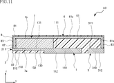
- the semiconductor device A3 according to the third embodiment of the present disclosure will be described with reference to FIG. In FIG. 11, elements that are the same as or similar to the semiconductor device A1 described above are designated by the same reference numerals, and duplicate description will be omitted.
- FIG. 11 is a cross-sectional view showing the semiconductor device A3, and is a diagram corresponding to FIG. 7 in the first embodiment.
- the semiconductor device A3 according to the present embodiment is different from the semiconductor device A1 in that the main surface 61a of the first plate portion is not exposed from the resin main surface 81 of the sealing resin 8.
- the connection lead 6 according to the third embodiment is entirely covered with the sealing resin 8.
- the semiconductor element 7 is flip-chip bonded, the inductance is reduced. Further, since the main current flows in the connection lead 6 in the direction opposite to the current path from the first lead 1 to the second lead 2, the generated magnetic fields cancel each other out, and the generated inductance is reduced. Further, since the connection lead 6 functions as a shielding plate for noise generated from the semiconductor element 7, the noise radiated from the semiconductor device A1 is reduced.
- the semiconductor device A4 according to the fourth embodiment of the present disclosure will be described with reference to FIG. In FIG. 12, elements that are the same as or similar to the semiconductor device A1 described above are designated by the same reference numerals, and duplicate description will be omitted.
- FIG. 12 is a cross-sectional view showing the semiconductor device A4, and is a diagram corresponding to FIG. 7 in the first embodiment.
- the semiconductor device A4 according to the present embodiment is different from the semiconductor device A1 in that the second plate portion 62 and the third plate portion 63 of the connection lead 6 are exposed from the resin side surface 83.
- the same effect as that of the first embodiment can be obtained. Further, according to the present embodiment, since the second plate portion 62 and the third plate portion 63 of the connection lead 6 are also exposed from the resin side surface 83, the heat dissipation property is further improved.
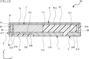
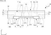
- FIGS. 13 and 14 elements that are the same as or similar to those of the semiconductor device A1 described above are designated by the same reference numerals, and redundant description will be omitted.
- FIG. 13 is a cross-sectional view showing the semiconductor device A5, which corresponds to FIG. 7 in the first embodiment.
- FIG. 14 is a front view showing the semiconductor device A5, and is a view corresponding to FIG. 4 in the first embodiment.
- the semiconductor device A5 according to the present embodiment is different from the semiconductor device A1 in that the connection method between the connection lead 6 and the second lead 2 and the third lead 3 is different.
- connection lead 6 does not include the second plate portion 62 and the third plate portion 63, but is only the first plate portion 61.
- the connection lead 6, the second lead 2, and the third lead 3 are each connected by two columnar portions 65.
- the columnar portion 65 is a conductor that connects the connection lead 6, the second lead 2, and the third lead 3.
- the columnar portion 65 has a prismatic shape having a rectangular cross section orthogonal to the z direction.
- the shape of the columnar portion 65 is not limited, and may be, for example, a cylindrical shape.
- One end (upper end in FIGS. 13 and 14) of the columnar portion 65 in the z direction is connected to the first plate portion 61 via a conductive bonding material (not shown).
- the other end of the columnar portion 65 in the z direction is a terminal portion main of the support portion main surface 211 of the second lead 2 or the third lead 3 via a conductive bonding material (not shown). It is connected to surface 311.
- the columnar portion 65 is made of, for example, Cu. The material, forming method, shape, and number of columnar portions 65 are not limited.
- connection lead 6, the second lead 2, and the third lead 3 are connected by the columnar portion 65
- connection lead 6, the second lead 2 and the third lead 3 may be connected by another conductive member such as a bonding wire.
- the semiconductor device A6 according to the sixth embodiment of the present disclosure will be described with reference to FIG. In FIG. 15, elements that are the same as or similar to those of the semiconductor device A1 described above are designated by the same reference numerals, and redundant description will be omitted.
- FIG. 15 is a cross-sectional view showing the semiconductor device A6, and is a diagram corresponding to FIG. 7 in the first embodiment.
- the semiconductor device A6 according to the present embodiment is different from the semiconductor device A1 in that the source terminal is arranged on a surface facing the opposite side of the drain terminal (first lead 1).
- the semiconductor device A6 according to the sixth embodiment does not include the second lead 2. Further, the connection lead 6 according to the sixth embodiment does not include the third plate portion 63.
- the first plate portion 61 of the connection lead 6 includes a protruding surface 61c protruding in the z direction from the main surface 61a of the first plate portion.
- the main surface 61a of the first plate portion is covered with the sealing resin 8.
- the protruding surface 61c is exposed from the sealing resin 8 and is flush with the resin main surface 81.
- the protruding surface 61c exposed from the sealing resin 8 serves as a source terminal.
- the same effect as that of the first embodiment can be obtained. Further, according to the present embodiment, since the second lead 2 is not arranged, the dimension in the y direction can be reduced.
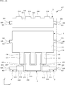
- FIGS. 16 and 17 elements that are the same as or similar to those of the semiconductor device A1 described above are designated by the same reference numerals, and redundant description will be omitted.
- FIG. 16 is a plan view showing the semiconductor device A7, and is a diagram corresponding to FIG. 3 in the first embodiment.
- the outer shape of the sealing resin 8 is shown by an imaginary line (dashed line) through the sealing resin 8, the connecting lead 6, and the semiconductor element 7.
- FIG. 17 is a right side view showing the semiconductor device A7, and is a view corresponding to FIG. 6 in the first embodiment.
- the semiconductor device A7 according to the present embodiment is different from the semiconductor device A1 in the shapes of the gate terminals (4th reed 4 and 5th reed 5) and the source terminals (3rd reed 3).
- the third reed 3 according to the seventh embodiment includes a protruding portion 314 protruding from the terminal end surface 313 in the y direction.
- the protruding portion 314 has a rectangular shape that is long in the x direction in the z direction.
- Four projecting portions 314 are arranged side by side at equal intervals in the x direction on the end surface of the terminal portion 310 facing outward in the y direction.
- the number of protrusions 314 is not limited.
- the terminal end surface 413 of the fourth lead 4 and the terminal end surface 513 of the fifth lead 5 are not flush with the resin side surface 83, but protrude from the resin side surface 83.
- the terminal end surface 413 of the 4th reed 4 and the terminal end surface 513 of the 5th reed 5 may be recessed from the resin side surface 83. Further, each of these end faces may be flat, curved, or uneven. Further, the shape of each of these end faces is not limited. Further, the terminal end surface 313 of the third lead 3 may be covered with the resin side surface 83, and the protruding portion 314 may be exposed from the resin side surface 83. Further, the third reed 3 may not have the protruding portion 314, and the terminal portion end surface 313 may be covered with the resin side surface 83.
- the semiconductor device A8 according to the eighth embodiment of the present disclosure will be described with reference to FIG. In FIG. 18, elements that are the same as or similar to the semiconductor device A1 described above are designated by the same reference numerals, and redundant description will be omitted.
- FIG. 18 is a plan view showing the semiconductor device A8, and is a diagram corresponding to FIG. 2 in the first embodiment.
- the outer shape of the sealing resin 8 is shown by an imaginary line (dashed line) through the sealing resin 8 and the connecting lead 6.
- the semiconductor device A8 according to the present embodiment is different from the semiconductor device A1 in the shapes of the drain electrode 71 and the source electrode 72 of the semiconductor element 7 and the shapes of the first lead 1 and the second lead 2.
- the first lead 1 has two extension portions 130, and the second lead 2 has one extension portion 230. Further, the drain electrode 71 includes two extension portions 712, and the source electrode 72 includes one extension portion 722.
- the number of extension portions 130 of the first lead 1 and the number of extension portions 230 of the second lead 2 are not limited. For example, there may be one extension portion 130 and two extension portions 230.
- the semiconductor device A9 according to the ninth embodiment of the present disclosure will be described with reference to FIG. In FIG. 19, elements that are the same as or similar to the semiconductor device A1 described above are designated by the same reference numerals, and redundant description will be omitted.
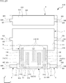
- FIG. 19 is a plan view showing the semiconductor device A9, and is a diagram corresponding to FIG. 2 in the first embodiment.
- the outer shape of the sealing resin 8 is shown by an imaginary line (dashed line) through the sealing resin 8 and the connecting lead 6.
- the semiconductor device A9 according to the present embodiment is different from the semiconductor device A1 in the shapes of the drain electrode 71 and the source electrode 72 of the semiconductor element 7 and the shapes of the first lead 1 and the second lead 2.
- the first lead 1 does not have the extension portion 130
- the second lead 2 does not have the extension portion 230
- the drain electrode 71 does not have an extension portion 712
- the source electrode 72 does not have an extension portion 722. That is, the semiconductor element 7 is a part of the terminal portion 110 of the first lead 1, a part of the support portion 210 of the second lead 2, a part of the terminal portion 410 of the fourth lead 4, and the terminal of the fifth lead 5. It is supported only by a part of part 510.
- the drain electrode 71 is bonded to the terminal main surface 111 of the first lead 1 only by the band-shaped portion 711
- the source electrode 72 is bonded to the support main surface 211 of the second lead 2 only by the band-shaped portion 721. There is.
- the semiconductor element 7 is flip-chip bonded, the inductance is reduced. Further, since the main current flows in the connection lead 6 in the direction opposite to the current path from the first lead 1 to the second lead 2, the generated magnetic fields cancel each other out, and the generated inductance is reduced. Further, since the connection lead 6 functions as a heat radiating plate that dissipates heat generated from the semiconductor element 7, the temperature rise of the semiconductor element 7 is suppressed. Further, since the connection lead 6 functions as a shielding plate for noise generated from the semiconductor element 7, the noise radiated from the semiconductor device A1 is reduced.
- the semiconductor device A10 according to the tenth embodiment of the present disclosure will be described with reference to FIG. In FIG. 20, elements that are the same as or similar to those of the semiconductor device A1 described above are designated by the same reference numerals, and redundant description will be omitted.
- FIG. 20 is a plan view showing the semiconductor device A10, and is a diagram corresponding to FIG. 2 in the first embodiment.
- the outer shape of the sealing resin 8 is shown by an imaginary line (dashed line) through the sealing resin 8 and the connecting lead 6.
- the shapes of the drain electrode 71 and the source electrode 72 of the semiconductor element 7 are different from those of the semiconductor device A1.
- the drain electrode 71 does not have a strip-shaped portion 711, and the source electrode 72 does not have a strip-shaped portion 721. That is, the drain electrode 71 is joined to the extension portion main surface 131 and the terminal portion main surface 111 of the first lead 1 only by the extension portion 712, and the source electrode 72 is joined to the second lead 2 only by the extension portion 722. It is joined to the main surface 231 of the extension portion and the main surface 211 of the support portion.
- the semiconductor device A11 according to the eleventh embodiment of the present disclosure will be described with reference to FIG. In FIG. 21, elements that are the same as or similar to the semiconductor device A1 described above are designated by the same reference numerals, and duplicate description will be omitted.
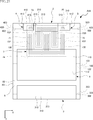
- FIG. 21 is a bottom view showing the semiconductor device A11, and is a diagram corresponding to FIG. 5 in the first embodiment.
- the back surface 212 of the support portion of the second lead 2 is exposed from the back surface 82 of the resin of the sealing resin 8, and the back surface 212 of the support portion and the back surface 82 of the resin are flush with each other. It is different from the semiconductor device A1.
- the semiconductor device A11 is surface-mounted on the circuit board, the second lead 2 is not joined to the wiring of the circuit board as a source terminal.
- the semiconductor device A12 according to the twelfth embodiment of the present disclosure will be described with reference to FIG. In FIG. 22, elements that are the same as or similar to those of the semiconductor device A1 described above are designated by the same reference numerals, and redundant description will be omitted.
- FIG. 22 is a bottom view showing the semiconductor device A12, and is a diagram corresponding to FIG. 5 in the first embodiment.
- the extension portion back surface 132 of the first lead 1 is exposed from the resin back surface 82 of the sealing resin 8, and the extension portion back surface 132 and the resin back surface 82 are flush with each other. Therefore, it is different from the semiconductor device A1. Since the back surface 232 of the extension portion of the second lead 2 is not exposed from the back surface 82 of the resin, the extension portion 130 and the extension portion 230 are connected by solder paste when the semiconductor device A12 is surface-mounted on the circuit board. Therefore, a short circuit between the first lead 1 and the second lead 2 is prevented.
- the same effect as that of the first embodiment can be obtained.
- the back surface 132 of the extension portion is exposed from the back surface 82 of the resin, when the semiconductor device A12 is surface-mounted on the circuit board, heat can be dissipated through the back surface 132 of the extension portion. it can. Therefore, the heat dissipation is further improved.
- the case where the back surface 132 of the extension portion of the first lead 1 is exposed from the back surface 82 of the resin and the back surface 232 of the extension portion of the second lead 2 is not exposed from the back surface 82 of the resin has been described. The same applies when the back surface 232 of the extension portion of the lead 2 is exposed from the back surface 82 of the resin and the back surface 132 of the extension portion of the first lead 1 is not exposed from the back surface 82 of the resin.
- the semiconductor device according to the present disclosure is not limited to the above-described embodiment.
- the specific configuration of each part of the semiconductor device according to the present disclosure can be freely redesigned.
- [Appendix 1] A semiconductor device having an electron traveling layer made of a nitride semiconductor, an element main surface and an element back surface facing opposite sides in the thickness direction, and a gate electrode, a source electrode, and a drain electrode arranged on the element main surface.
- the main current which is the target of switching, flows through the connection lead.
- Semiconductor device Semiconductor device.
- Appendix 2 The semiconductor device according to Appendix 1, wherein the connection lead is in contact with the back surface of the device.
- the semiconductor element further includes a back surface electrode arranged on the back surface of the device and electrically connected to the source electrode.
- the semiconductor device according to Appendix 2 wherein the back surface electrode is bonded to the connection lead.
- [Appendix 4] Further provided with a sealing resin covering the semiconductor element, The semiconductor device according to any one of Supplementary note 1 to 3, wherein a part of the connection lead is exposed from the sealing resin.
- [Appendix 5] The semiconductor device according to Appendix 4, wherein the sealing resin has a resin main surface and a resin back surface facing opposite sides in the thickness direction, and a resin side surface connected to the resin main surface and the resin back surface.
- connection lead The semiconductor device according to Appendix 5, wherein the second lead is not exposed from the resin main surface and the resin back surface.
- connection lead is a metal plate.
- the connection lead includes a first plate-shaped portion that overlaps the semiconductor element in the thickness direction, and A second plate-shaped portion connected to the second lead and the first plate-shaped portion, 7.
- a third lead arranged on the side opposite to the second lead is further provided with respect to the first lead.
- the semiconductor device according to Appendix 8, wherein the connection lead further includes a third plate-shaped portion that connects the third lead and the first plate-shaped portion.
- [Appendix 10] The semiconductor device according to Appendix 9, wherein the second plate-shaped portion and the third plate-shaped portion are parallel to the thickness direction.
- Appendix 11 The semiconductor device according to Appendix 9 or 10, wherein the first lead and a part of the third lead are exposed from the back surface of the resin.
- Appendix 12 The third lead has a third end surface that faces the opposite side of the first lead and is exposed from the resin side surface.
- the semiconductor device according to any one of Supplementary note 5 to 12, further comprising a fourth lead arranged on the same side as the second lead with respect to the first lead and to which the gate electrode is bonded. ..
- the fourth lead has a fourth end surface that faces the opposite side of the first lead and is exposed from the resin side surface.
- the semiconductor device according to Appendix 13, wherein the fourth end surface and the resin side surface are flush with each other.
- the first lead includes a plurality of first extending portions extending toward the second lead side in the thickness direction.
- the second lead includes a second extension portion that extends toward the first lead side in the thickness direction and is arranged between the plurality of first extension portions.
- the semiconductor device according to any one of Supplementary note 4 to 14, wherein the semiconductor element is supported by the first extension portion and the second extension portion.
- the second lead includes a plurality of second extending portions extending toward the first lead side in the thickness direction.
- the first lead includes a first extension portion that extends toward the second lead side in the thickness direction and is arranged between the plurality of second extension portions.
- the semiconductor device according to any one of Supplementary note 4 to 14, wherein the semiconductor element is supported by the first extension portion and the second extension portion.
- the first lead includes two or more of the first extending portions.
- the second lead includes two or more of the second extending portions.
- the first extension portion and the second extension portion are alternately arranged in a direction orthogonal to the extension direction and the thickness direction of the first extension portion, according to Appendix 15 or 16.
- Semiconductor device [Appendix 18] The semiconductor device according to any one of Appendix 15 to 17, wherein the first extending portion and the second extending portion are covered with the sealing resin.
- A1 to A12 Semiconductor device 1: First lead 110: Terminal 111: Terminal main surface 112: Terminal back surface 120: Connecting unit 121: Connecting unit main surface 122: Connecting unit back surface 123: Connecting unit end surface 130: Extension Part 131: Extension part main surface 132: Extension part back surface 2: Second lead 210: Support part 211: Support part main surface 212: Support part back surface 213: Support part end surface 230: Extension part 231: Extension part main surface Surface 232: Extended portion back surface 3: Third lead 310: Terminal portion 311: Terminal portion main surface 312: Terminal portion back surface 313: Terminal portion end surface 314: Protruding portion 320: Connecting portion 321: Connecting portion main surface 322: Connecting portion Back surface 323: Connection part end surface 4: Fourth lead 410: Terminal part 411: Terminal part main surface 412: Terminal part back surface 413: Terminal part end surface 420: Connection part 421: Connection part main surface 422: Connection part back surface 423: Connection part End face 5: Fifth lead
Landscapes
- Electrodes Of Semiconductors (AREA)
- Junction Field-Effect Transistors (AREA)
- Structures Or Materials For Encapsulating Or Coating Semiconductor Devices Or Solid State Devices (AREA)
- Lead Frames For Integrated Circuits (AREA)
Priority Applications (2)
| Application Number | Priority Date | Filing Date | Title |
|---|---|---|---|
| JP2021529962A JP7562529B2 (ja) | 2019-07-01 | 2020-06-19 | 半導体装置 |
| US17/596,926 US12165957B2 (en) | 2019-07-01 | 2020-06-19 | Semiconductor device |
Applications Claiming Priority (2)
| Application Number | Priority Date | Filing Date | Title |
|---|---|---|---|
| JP2019122873 | 2019-07-01 | ||
| JP2019-122873 | 2019-07-01 |
Publications (1)
| Publication Number | Publication Date |
|---|---|
| WO2021002225A1 true WO2021002225A1 (ja) | 2021-01-07 |
Family
ID=74100598
Family Applications (1)
| Application Number | Title | Priority Date | Filing Date |
|---|---|---|---|
| PCT/JP2020/024238 Ceased WO2021002225A1 (ja) | 2019-07-01 | 2020-06-19 | 半導体装置 |
Country Status (3)
| Country | Link |
|---|---|
| US (1) | US12165957B2 (https=) |
| JP (1) | JP7562529B2 (https=) |
| WO (1) | WO2021002225A1 (https=) |
Cited By (2)
| Publication number | Priority date | Publication date | Assignee | Title |
|---|---|---|---|---|
| JP2022144459A (ja) * | 2021-03-19 | 2022-10-03 | ローム株式会社 | 半導体装置 |
| WO2024181293A1 (ja) * | 2023-03-01 | 2024-09-06 | ローム株式会社 | 半導体装置 |
Citations (5)
| Publication number | Priority date | Publication date | Assignee | Title |
|---|---|---|---|---|
| JPH05121615A (ja) * | 1991-10-25 | 1993-05-18 | Rohm Co Ltd | 半導体装置 |
| JPH07201914A (ja) * | 1993-12-29 | 1995-08-04 | Nippon Steel Corp | 半導体装置及びその製造方法 |
| JP2005175512A (ja) * | 2005-02-16 | 2005-06-30 | Nec Electronics Corp | 半導体装置 |
| JP2013222781A (ja) * | 2012-04-16 | 2013-10-28 | Sharp Corp | 半導体装置のデバイス実装構造 |
| JP2018056538A (ja) * | 2016-09-26 | 2018-04-05 | 株式会社パウデック | 半導体パッケージ、モジュールおよび電気機器 |
Family Cites Families (4)
| Publication number | Priority date | Publication date | Assignee | Title |
|---|---|---|---|---|
| JP6211829B2 (ja) | 2013-06-25 | 2017-10-11 | 株式会社東芝 | 半導体装置 |
| KR20150127440A (ko) | 2014-05-07 | 2015-11-17 | 삼성전기주식회사 | 탄탈륨 캐패시터 및 그 제조방법 |
| JP6827776B2 (ja) | 2016-11-15 | 2021-02-10 | ローム株式会社 | 半導体デバイス |
| JP7009157B2 (ja) | 2016-12-28 | 2022-01-25 | ローム株式会社 | 半導体装置 |
-
2020
- 2020-06-19 US US17/596,926 patent/US12165957B2/en active Active
- 2020-06-19 WO PCT/JP2020/024238 patent/WO2021002225A1/ja not_active Ceased
- 2020-06-19 JP JP2021529962A patent/JP7562529B2/ja active Active
Patent Citations (5)
| Publication number | Priority date | Publication date | Assignee | Title |
|---|---|---|---|---|
| JPH05121615A (ja) * | 1991-10-25 | 1993-05-18 | Rohm Co Ltd | 半導体装置 |
| JPH07201914A (ja) * | 1993-12-29 | 1995-08-04 | Nippon Steel Corp | 半導体装置及びその製造方法 |
| JP2005175512A (ja) * | 2005-02-16 | 2005-06-30 | Nec Electronics Corp | 半導体装置 |
| JP2013222781A (ja) * | 2012-04-16 | 2013-10-28 | Sharp Corp | 半導体装置のデバイス実装構造 |
| JP2018056538A (ja) * | 2016-09-26 | 2018-04-05 | 株式会社パウデック | 半導体パッケージ、モジュールおよび電気機器 |
Cited By (3)
| Publication number | Priority date | Publication date | Assignee | Title |
|---|---|---|---|---|
| JP2022144459A (ja) * | 2021-03-19 | 2022-10-03 | ローム株式会社 | 半導体装置 |
| JP7636219B2 (ja) | 2021-03-19 | 2025-02-26 | ローム株式会社 | 半導体装置 |
| WO2024181293A1 (ja) * | 2023-03-01 | 2024-09-06 | ローム株式会社 | 半導体装置 |
Also Published As
| Publication number | Publication date |
|---|---|
| US20220319964A1 (en) | 2022-10-06 |
| JP7562529B2 (ja) | 2024-10-07 |
| US12165957B2 (en) | 2024-12-10 |
| JPWO2021002225A1 (https=) | 2021-01-07 |
Similar Documents
| Publication | Publication Date | Title |
|---|---|---|
| JP7520177B2 (ja) | 半導体装置 | |
| JP7441287B2 (ja) | 半導体装置 | |
| JP6726112B2 (ja) | 半導体装置および電力変換装置 | |
| CN102074538A (zh) | 半导体装置及其引线框 | |
| JP2020188177A (ja) | 半導体装置 | |
| JP2022143169A (ja) | 半導体装置 | |
| US10535625B2 (en) | Semiconductor device with first and second transistors and support part | |
| JP7562529B2 (ja) | 半導体装置 | |
| JP7222822B2 (ja) | 半導体装置 | |
| JP7835681B2 (ja) | 半導体装置 | |
| JP7582301B2 (ja) | 半導体装置 | |
| KR101824725B1 (ko) | 반도체 패키지 | |
| JP2021190556A (ja) | 半導体装置の実装構造 | |
| JP2023104908A (ja) | 半導体装置 | |
| JP7385414B2 (ja) | 半導体装置 | |
| US12463119B2 (en) | Semiconductor device and semiconductor device manufacturing method | |
| JP2006294729A (ja) | 半導体装置 | |
| JP2020167233A (ja) | モジュールおよびその製造方法 | |
| WO2024057876A1 (ja) | 半導体装置 | |
| WO2024225011A1 (ja) | 半導体装置、および、半導体装置の製造方法 | |
| CN110892527A (zh) | 半导体装置以及半导体装置的制造方法 |
Legal Events
| Date | Code | Title | Description |
|---|---|---|---|
| 121 | Ep: the epo has been informed by wipo that ep was designated in this application |
Ref document number: 20834379 Country of ref document: EP Kind code of ref document: A1 |
|
| ENP | Entry into the national phase |
Ref document number: 2021529962 Country of ref document: JP Kind code of ref document: A |
|
| NENP | Non-entry into the national phase |
Ref country code: DE |
|
| 122 | Ep: pct application non-entry in european phase |
Ref document number: 20834379 Country of ref document: EP Kind code of ref document: A1 |