WO2020262368A1 - 静電チャックヒータ - Google Patents
静電チャックヒータ Download PDFInfo
- Publication number
- WO2020262368A1 WO2020262368A1 PCT/JP2020/024573 JP2020024573W WO2020262368A1 WO 2020262368 A1 WO2020262368 A1 WO 2020262368A1 JP 2020024573 W JP2020024573 W JP 2020024573W WO 2020262368 A1 WO2020262368 A1 WO 2020262368A1
- Authority
- WO
- WIPO (PCT)
- Prior art keywords
- layer
- electrostatic chuck
- heater
- ceramic
- thickness
- Prior art date
- Legal status (The legal status is an assumption and is not a legal conclusion. Google has not performed a legal analysis and makes no representation as to the accuracy of the status listed.)
- Ceased
Links
Images

Classifications
-
- H—ELECTRICITY
- H10—SEMICONDUCTOR DEVICES; ELECTRIC SOLID-STATE DEVICES NOT OTHERWISE PROVIDED FOR
- H10P—GENERIC PROCESSES OR APPARATUS FOR THE MANUFACTURE OR TREATMENT OF DEVICES COVERED BY CLASS H10
- H10P72/00—Handling or holding of wafers, substrates or devices during manufacture or treatment thereof
- H10P72/70—Handling or holding of wafers, substrates or devices during manufacture or treatment thereof for supporting or gripping
- H10P72/72—Handling or holding of wafers, substrates or devices during manufacture or treatment thereof for supporting or gripping using electrostatic chucks
-
- H—ELECTRICITY
- H10—SEMICONDUCTOR DEVICES; ELECTRIC SOLID-STATE DEVICES NOT OTHERWISE PROVIDED FOR
- H10P—GENERIC PROCESSES OR APPARATUS FOR THE MANUFACTURE OR TREATMENT OF DEVICES COVERED BY CLASS H10
- H10P72/00—Handling or holding of wafers, substrates or devices during manufacture or treatment thereof
- H10P72/04—Apparatus for manufacture or treatment
- H10P72/0431—Apparatus for thermal treatment
- H10P72/0432—Apparatus for thermal treatment mainly by conduction
-
- B—PERFORMING OPERATIONS; TRANSPORTING
- B23—MACHINE TOOLS; METAL-WORKING NOT OTHERWISE PROVIDED FOR
- B23Q—DETAILS, COMPONENTS, OR ACCESSORIES FOR MACHINE TOOLS, e.g. ARRANGEMENTS FOR COPYING OR CONTROLLING; MACHINE TOOLS IN GENERAL CHARACTERISED BY THE CONSTRUCTION OF PARTICULAR DETAILS OR COMPONENTS; COMBINATIONS OR ASSOCIATIONS OF METAL-WORKING MACHINES, NOT DIRECTED TO A PARTICULAR RESULT
- B23Q3/00—Devices holding, supporting, or positioning work or tools, of a kind normally removable from the machine
- B23Q3/15—Devices for holding work using magnetic or electric force acting directly on the work
-
- H—ELECTRICITY
- H02—GENERATION; CONVERSION OR DISTRIBUTION OF ELECTRIC POWER
- H02N—ELECTRIC MACHINES NOT OTHERWISE PROVIDED FOR
- H02N13/00—Clutches or holding devices using electrostatic attraction, e.g. using Johnson-Rahbek effect
-
- H—ELECTRICITY
- H05—ELECTRIC TECHNIQUES NOT OTHERWISE PROVIDED FOR
- H05B—ELECTRIC HEATING; ELECTRIC LIGHT SOURCES NOT OTHERWISE PROVIDED FOR; CIRCUIT ARRANGEMENTS FOR ELECTRIC LIGHT SOURCES, IN GENERAL
- H05B1/00—Details of electric heating devices
- H05B1/02—Automatic switching arrangements specially adapted to apparatus ; Control of heating devices
- H05B1/0227—Applications
- H05B1/023—Industrial applications
- H05B1/0233—Industrial applications for semiconductors manufacturing
-
- H—ELECTRICITY
- H05—ELECTRIC TECHNIQUES NOT OTHERWISE PROVIDED FOR
- H05B—ELECTRIC HEATING; ELECTRIC LIGHT SOURCES NOT OTHERWISE PROVIDED FOR; CIRCUIT ARRANGEMENTS FOR ELECTRIC LIGHT SOURCES, IN GENERAL
- H05B3/00—Ohmic-resistance heating
- H05B3/02—Details
-
- H—ELECTRICITY
- H05—ELECTRIC TECHNIQUES NOT OTHERWISE PROVIDED FOR
- H05B—ELECTRIC HEATING; ELECTRIC LIGHT SOURCES NOT OTHERWISE PROVIDED FOR; CIRCUIT ARRANGEMENTS FOR ELECTRIC LIGHT SOURCES, IN GENERAL
- H05B3/00—Ohmic-resistance heating
- H05B3/02—Details
- H05B3/06—Heater elements structurally combined with coupling elements or holders
-
- H—ELECTRICITY
- H05—ELECTRIC TECHNIQUES NOT OTHERWISE PROVIDED FOR
- H05B—ELECTRIC HEATING; ELECTRIC LIGHT SOURCES NOT OTHERWISE PROVIDED FOR; CIRCUIT ARRANGEMENTS FOR ELECTRIC LIGHT SOURCES, IN GENERAL
- H05B3/00—Ohmic-resistance heating
- H05B3/20—Heating elements having extended surface area substantially in a two-dimensional [2D] plane, e.g. plate-heater
- H05B3/22—Heating elements having extended surface area substantially in a two-dimensional [2D] plane, e.g. plate-heater non-flexible
- H05B3/28—Heating elements having extended surface area substantially in a two-dimensional [2D] plane, e.g. plate-heater non-flexible heating conductor embedded in insulating material
- H05B3/283—Heating elements having extended surface area substantially in a two-dimensional [2D] plane, e.g. plate-heater non-flexible heating conductor embedded in insulating material the insulating material being an inorganic material, e.g. ceramic
-
- H—ELECTRICITY
- H05—ELECTRIC TECHNIQUES NOT OTHERWISE PROVIDED FOR
- H05B—ELECTRIC HEATING; ELECTRIC LIGHT SOURCES NOT OTHERWISE PROVIDED FOR; CIRCUIT ARRANGEMENTS FOR ELECTRIC LIGHT SOURCES, IN GENERAL
- H05B3/00—Ohmic-resistance heating
- H05B3/68—Heating arrangements specially adapted for cooking plates or analogous hot-plates
- H05B3/74—Non-metallic plates, e.g. vitroceramic, ceramic or glassceramic hobs, also including power or control circuits
- H05B3/748—Resistive heating elements, i.e. heating elements exposed to the air, e.g. coil wire heater
-
- H—ELECTRICITY
- H10—SEMICONDUCTOR DEVICES; ELECTRIC SOLID-STATE DEVICES NOT OTHERWISE PROVIDED FOR
- H10P—GENERIC PROCESSES OR APPARATUS FOR THE MANUFACTURE OR TREATMENT OF DEVICES COVERED BY CLASS H10
- H10P72/00—Handling or holding of wafers, substrates or devices during manufacture or treatment thereof
- H10P72/04—Apparatus for manufacture or treatment
- H10P72/0431—Apparatus for thermal treatment
- H10P72/0434—Apparatus for thermal treatment mainly by convection
-
- H—ELECTRICITY
- H10—SEMICONDUCTOR DEVICES; ELECTRIC SOLID-STATE DEVICES NOT OTHERWISE PROVIDED FOR
- H10P—GENERIC PROCESSES OR APPARATUS FOR THE MANUFACTURE OR TREATMENT OF DEVICES COVERED BY CLASS H10
- H10P72/00—Handling or holding of wafers, substrates or devices during manufacture or treatment thereof
- H10P72/70—Handling or holding of wafers, substrates or devices during manufacture or treatment thereof for supporting or gripping
- H10P72/72—Handling or holding of wafers, substrates or devices during manufacture or treatment thereof for supporting or gripping using electrostatic chucks
- H10P72/722—Details of electrostatic chucks
-
- H—ELECTRICITY
- H10—SEMICONDUCTOR DEVICES; ELECTRIC SOLID-STATE DEVICES NOT OTHERWISE PROVIDED FOR
- H10P—GENERIC PROCESSES OR APPARATUS FOR THE MANUFACTURE OR TREATMENT OF DEVICES COVERED BY CLASS H10
- H10P72/00—Handling or holding of wafers, substrates or devices during manufacture or treatment thereof
- H10P72/70—Handling or holding of wafers, substrates or devices during manufacture or treatment thereof for supporting or gripping
- H10P72/76—Handling or holding of wafers, substrates or devices during manufacture or treatment thereof for supporting or gripping using mechanical means, e.g. clamps or pinches
- H10P72/7604—Handling or holding of wafers, substrates or devices during manufacture or treatment thereof for supporting or gripping using mechanical means, e.g. clamps or pinches the wafers being placed on a susceptor, stage or support
- H10P72/7616—Handling or holding of wafers, substrates or devices during manufacture or treatment thereof for supporting or gripping using mechanical means, e.g. clamps or pinches the wafers being placed on a susceptor, stage or support characterised by a coating, a hardness or a material
Definitions
- the present invention relates to an electrostatic chuck heater.
- an electrostatic chuck heater that adsorbs and holds a wafer is used in a film forming process such as transporting, exposing, and CVD of a semiconductor wafer, and in microfabrication such as cleaning, etching, and dicing.
- a film forming process such as transporting, exposing, and CVD of a semiconductor wafer
- microfabrication such as cleaning, etching, and dicing.
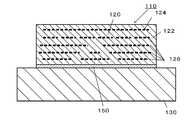
- an electrostatic chuck heater as shown in FIG. 3, an electrostatic chuck 120 in which an electrostatic electrode 124 and a plurality of metal layers 126 (including a resistance heating element layer) are embedded in a ceramic sintered body 122, and a static electricity chuck 120 thereof.
- An electrostatic chuck heater 110 in which a cooling member 130 for cooling an electric chuck 120 is bonded with an adhesive layer 150 is known.
- Patent Document 1 As shown in FIG. 4, an electrostatic chuck 220 in which an electrostatic electrode 224 is embedded in a ceramic sintered body 222, a cooling member 230 for cooling the electrostatic chuck 220, and electrostatic electricity
- An electrostatic chuck heater 210 including a seat heater 240 provided between the chuck 220 and the cooling member 230 is also known.
- a plurality of metal layers 242 including a resistance heating element layer are embedded in a resin sheet 241 in multiple stages.
- the sheet heater 240 is adhered to the electrostatic chuck 220 and the cooling member 230 via an adhesive layer 250, respectively.
- the combined thickness of the electrostatic chuck 220 and the sheet heater 240 in the electrostatic chuck heater 210 of FIG. 4 can be made thinner than the thickness of the ceramic sintered body 122 of FIG.
- the seat heater 240 provided between the electrostatic chuck 220 and the cooling member 230 has a large thermal resistance, the wafer electrostatically attracted to the electrostatic chuck 220 receives external heat such as plasma heat input. There was a problem that it was difficult to cool quickly in some cases.
- the present invention has been made to solve such a problem, and its main purpose is to improve the processing capacity against external heat input.
- the electrostatic chuck heater of the present invention An electrostatic chuck with electrostatic electrodes embedded in a ceramic sintered body, A cooling member that cools the electrostatic chuck and A heater layer provided between the electrostatic chuck and the cooling member, in which a plurality of metal layers including a resistance heating element layer are embedded in multiple stages.
- the heater layer has a ceramic insulating layer having a thickness of 2 ⁇ m or more and 50 ⁇ m or less between the metal layers. It is a thing.
- the heater layer has a ceramic insulating layer having a thickness of 2 ⁇ m or more and 50 ⁇ m or less between the metal layers.
- the thickness of the ceramic insulating layer is within this numerical range, the withstand voltage normally required for the resistance heating element layer is satisfied.
- the overall thickness of the heater layer is reduced, and the heat capacity of the heater layer is reduced.
- ceramic is superior in thermal conductivity to resin. As a result, the thermal resistance of the heater layer provided between the electrostatic chuck and the cooling member becomes small, and when the wafer electrostatically adsorbed by the electrostatic chuck receives external heat such as plasma heat input, it is quick. Can be cooled to.
- the processing capacity against external heat input is improved.
- the withstand voltage per layer of the ceramic insulating layer is preferably AC200V or more. In this way, it is possible to sufficiently prevent dielectric breakdown when used as an electrostatic chuck heater.
- the porosity of the ceramic insulating layer is preferably 0.5% or less.
- the heater layer preferably has three or more ceramic insulating layers, and more preferably five or more layers. In this way, it is possible to easily design a multi-zone heater (an electrostatic chuck is divided into a plurality of zones and a resistance heating element is arranged in each zone).
- the ceramic insulating layer may be an aerosol deposition (AD) film.
- AD is suitable for accurately forming a thin film of fine ceramic particles. Further, since AD can form ceramic particles by the impact solidification phenomenon, it is not necessary to sinter the ceramic particles at a high temperature.
- the metal layer may be an AD film, a CVD film, a PVD film, or a plating film.
- the metal layer may be formed by printing or the like, but is preferably formed by an AD method (including a plasma AD method), a CVD method, a PVD method, a plating method, or the like. These are suitable for accurately forming a thin film of fine metal particles. Moreover, it is not necessary to use a paste in which metal particles are mixed with a resin component.
- the metal layer may include a jumper wire layer in which a jumper wire for supplying electric power to the resistance heating element layer is wired.
- a jumper wire layer in which a jumper wire for supplying electric power to the resistance heating element layer is wired.
- one resistance heating element layer is divided into a plurality of zones and resistance heating elements are arranged in each zone, it is preferable to provide a jumper wire layer.
- the vertical sectional view of the electrostatic chuck heater of this embodiment A vertical cross-sectional view of a sample prototyped in an experimental example. Longitudinal section of a conventional electrostatic chuck heater. Longitudinal section of a conventional electrostatic chuck heater.
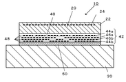
- FIG. 1 is a vertical cross-sectional view of the electrostatic chuck heater of the present embodiment.
- the electrostatic chuck heater 10 includes an electrostatic chuck 20, a cooling member 30, and a heater layer 40.
- the electrostatic chuck 20 has an electrostatic electrode 24 embedded in a disk-shaped ceramic sintered body 22, and is placed on the upper surface of the electrostatic chuck 20 when a voltage is applied to the electrostatic electrode 24.
- the wafer (not shown) is electrostatically attracted.
- the cooling member 30 is a metal member having a refrigerant passage (not shown) inside, and cools the electrostatic chuck 20.
- the heater layer 40 is provided between the electrostatic chuck 20 and the cooling member 30, and a plurality of metal layers 42 including resistance heating element layers 44a and 44b and jumper wire layers 46a and 46b are embedded in multiple stages. ..
- the heater layer 40 is directly formed on the surface of the electrostatic chuck 20 opposite to the wafer adsorption surface, and is adhered to the cooling member 30 via the adhesive layer 50.
- the heater layer 40 has a ceramic insulating layer 48 having a thickness of 2 ⁇ m or more and 50 ⁇ m or less between the metal layers 42.
- the ceramic insulating layer 48 is preferably an AD film formed by an AD method using ceramic particles.
- the AD film has higher insulating properties than the thermal sprayed film and can be made thinner.
- the metal layer 42 is preferably an AD film formed by an AD method using metal particles, or a metal layer 42 formed by a CVD method, a PVD method, or a plating method.
- the metal layer 42 includes an upper resistance heating element layer 44a, an upper jumper wire layer 46a, a lower jumper wire layer 46b, and a lower resistance heating element layer 44b.
- the upper resistance heating element layer 44a is divided into a large number of zones, and a resistance heating element is wired for each zone.
- the resistance heating element is wired from one end to the other end in a one-stroke manner so as to cover the entire zone.
- the lower resistance heating element layer 44b is divided into a smaller number of zones than the upper resistance heating element layer, and the resistance heating element is wired for each zone.
- the upper and lower jumper wire layers 46a and 46b each have a plurality of jumper wires. The jumper wire supplies electric power from the heater power supply to each of the resistance heating elements included in the upper and lower resistance heating element layers 44a and 44b.
- the heater layer 40 has a ceramic insulating layer 48 having a thickness of 2 ⁇ m or more and 50 ⁇ m or less between the metal layers 42.
- the thickness of the ceramic insulating layer 48 is within this numerical range, the withstand voltage normally required for the resistance heating element layers 44a and 44b is satisfied.
- the overall thickness of the heater layer 40 is reduced, and the heat capacity of the heater layer 40 is reduced.
- ceramic is superior in thermal conductivity to resin. As a result, the thermal resistance of the heater layer 40 provided between the electrostatic chuck 20 and the cooling member 30 becomes small, and the wafer electrostatically attracted to the electrostatic chuck 20 receives external heat such as plasma heat input. If it does, it can be cooled quickly.
- the processing capacity for external heat input is improved.
- the withstand voltage (dielectric strength) per layer of the ceramic insulating layer 48 is preferably AC200V or more. By doing so, it is possible to sufficiently prevent dielectric breakdown from occurring when the electrostatic chuck heater 10 is used.
- the porosity of the ceramic insulating layer 48 is preferably 0.5% or less.
- the heater layer 40 preferably has three or more ceramic insulating layers 48, and more preferably five or more layers. In this way, a multi-zone heater can be easily designed.
- the ceramic insulating layer 48 is preferably an AD film.
- AD is suitable for accurately forming a thin layer of fine ceramic particles. Further, since AD can form ceramic particles by the impact solidification phenomenon, it is not necessary to sinter the ceramic particles at a high temperature.
- the metal layer 42 includes jumper wire layers 46a and 46b in which jumper wires for supplying electric power to the resistance heating element layers 44a and 44b are wired.
- jumper wire layers 46a and 46b in which jumper wires for supplying electric power to the resistance heating element layers 44a and 44b are wired.
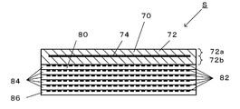
- Example 1-6 As shown in FIG. 2, a sample S in which the electrostatic chuck 70 and the heater layer 80 are laminated was prepared.
- the electrostatic chuck 70 has a structure in which an electrostatic electrode 74 is embedded in an alumina ceramic sintered body 72 having a diameter of ⁇ 300 mm.
- the upper layer is referred to as a dielectric layer 72a and the lower layer is referred to as an insulating layer 72b with the electrostatic electrode 74 as a boundary.
- the thickness of the dielectric layer 72a was 0.4 [mm]
- the thickness of the insulating layer 72b was 0.5 [mm].
- the heater layer 80 has a structure having six metal layers 82 inside, an interlayer insulating film 84 made of alumina ceramic is provided between the metal layers 82, and the back surface insulation made of alumina ceramic is provided on the back surface of the metal layer 82 of the lowermost layer.
- the film 86 was provided.
- Experimental Example 1-4 first, an electrostatic chuck 70 was manufactured. Subsequently, one metal layer 82 was formed on the back surface of the electrostatic chuck 70, and then one insulating film (interlayer insulating film 84) was formed so as to cover the metal layer 82 by the AD method. Subsequently, a sample S was prepared by repeatedly forming one metal layer 82 on the back surface of the insulating film and then forming one insulating film so as to cover the metal layer 82 by the AD method. The last insulating film was the back surface insulating film 86. In Experimental Example 5, Sample S was prepared in the same manner as in Experimental Example 1-4 except that the thermal spraying method was adopted instead of the AD method.
- Table 1 summarizes the thickness of the dielectric layer 72a, the thickness of the insulating layer 72b, the total number of metal layers 82, the information on the interlayer insulating film 84, the thickness of the backside insulating film 86, and the information on the sample S.
- the information regarding the interlayer insulating film 84 the material, the number of layers, the manufacturing method, the thickness, the withstand voltage, and the total thickness are shown.
- the withstand voltage was measured by applying a potential difference of AC to both sides of the interlayer insulating film 84.
- the total thickness, thermal resistance (heat removal performance), and time required for raising the temperature to 50 ° C. at 1 kW are shown.
- the thickness of the interlayer insulating film 84 (AD film) was 60 ⁇ m, cracks occurred.
- the cause of the crack is considered to be that the internal stress of the AD film has increased. From the above, it was found that the thickness of the interlayer insulating film 84 is preferably 2 ⁇ m or more and 50 ⁇ m or less.
- the withstand voltage (AC200 V or more) normally required for each layer was satisfied.
- the overall thickness of the heater layer 80 was as thin as 0.5 mm or less, the heat capacity and thermal resistance of the heater layer 80 were relatively small, and the time required to raise the temperature to 50 ° C. at 1 kW was also relatively short. However, the time was slightly longer than that of the AD film. It is considered that the cause is that the porosity of the sprayed film was several percent, which was higher than the porosity of the AD film (0.5% or less).
- the overall thickness of the heater layer 80 was 1 although the withstand voltage (AC200V or more) normally required for each layer was satisfied. As thick as .25 mm, the heat capacity and thermal resistance of the heater layer 80 increased, and the time required to raise the temperature to 50 ° C. at 1 kW became longer. Although not shown in Table 1, even when powder molding is used instead of tape molding, the overall thickness of the heater layer 80 is further increased to 3 mm, and the time required to raise the temperature to 50 ° C. at 1 kW is long. It exceeded 40 seconds.
- the buried position inside the ceramic varies due to firing strain, so that the back surface insulating film 84 needs to be thicker than when manufactured by the AD method or the thermal spraying method. This increases the heat capacity and thermal resistance.
- Experimental Examples 1, 2 and 5 correspond to Examples of the present invention
- Experimental Examples 3, 4 and 6 correspond to Comparative Examples. It goes without saying that these examples do not limit the present invention in any way.
- the electrostatic chuck heater of the present invention can be used, for example, for film forming processes such as semiconductor wafer transfer, exposure, and CVD, and for microfabrication such as cleaning, etching, and dicing.
Landscapes
- Engineering & Computer Science (AREA)
- Chemical & Material Sciences (AREA)
- Ceramic Engineering (AREA)
- Inorganic Chemistry (AREA)
- Mechanical Engineering (AREA)
- Manufacturing & Machinery (AREA)
- Container, Conveyance, Adherence, Positioning, Of Wafer (AREA)
- Resistance Heating (AREA)
Abstract
Description
セラミック焼結体に静電電極が埋設された静電チャックと、
前記静電チャックを冷却する冷却部材と、
前記静電チャックと前記冷却部材との間に設けられ、抵抗発熱体層を含む複数の金属層が多段に埋設されたヒータ層と、
を備え、
前記ヒータ層は、前記金属層同士の間に厚さが2μm以上50μm以下のセラミック絶縁層を有する、
ものである。
図2に示すように、静電チャック70とヒータ層80とを積層したサンプルSを作製した。静電チャック70は、直径φ300mmのアルミナセラミック焼結体72に静電電極74を埋設した構造とした。アルミナセラミック焼結体72のうち静電電極74を境界にして上側の層を誘電体層72a、下側の層を絶縁層72bと称する。誘電体層72aの厚みは0.4[mm]、絶縁層72bの厚みは0.5[mm]とした。ヒータ層80は、内部に金属層82を6層有する構造とし、金属層82同士の間にアルミナセラミック製の層間絶縁膜84を設け、最下層の金属層82の裏面にアルミナセラミック製の裏面絶縁膜86を設けた。

Claims (7)
- セラミック焼結体に静電電極が埋設された静電チャックと、
前記静電チャックを冷却する冷却部材と、
前記静電チャックと前記冷却部材との間に設けられ、抵抗発熱体層を含む複数の金属層が多段に埋設されたヒータ層と、
を備え、
前記ヒータ層は、前記金属層同士の間に厚さが2μm以上50μm以下のセラミック絶縁層を有する、
静電チャックヒータ。 - 前記セラミック絶縁層の1層当たりの耐電圧は、AC200V以上である、
請求項1に記載の静電チャックヒータ。 - 前記セラミック絶縁層の気孔率は、0.5%以下である、
請求項1又は2に記載の静電チャックヒータ。 - 前記ヒータ層は、前記セラミック絶縁層を3層以上有する、
請求項1~3のいずれか1項に記載の静電チャックヒータ。 - 前記セラミック絶縁層は、エアロゾルデポジション膜である、
請求項1~4のいずれか1項に記載の静電チャックヒータ。 - 前記金属層は、エアロゾルデポジション膜である、
請求項1~5のいずれか1項に記載の静電チャックヒータ。 - 前記金属層は、前記抵抗発熱体層に電力を供給するジャンパ線が配線されたジャンパ線層を含む、
請求項1~6のいずれか1項に記載の静電チャックヒータ。
Priority Applications (4)
| Application Number | Priority Date | Filing Date | Title |
|---|---|---|---|
| JP2021527636A JP7522110B2 (ja) | 2019-06-28 | 2020-06-23 | 静電チャックヒータ |
| KR1020217033742A KR102797839B1 (ko) | 2019-06-28 | 2020-06-23 | 정전 척 히터 |
| CN202080047681.0A CN114080670B (zh) | 2019-06-28 | 2020-06-23 | 静电卡盘加热器 |
| US17/451,504 US12230526B2 (en) | 2019-06-28 | 2021-10-20 | Electrostatic chuck heater |
Applications Claiming Priority (2)
| Application Number | Priority Date | Filing Date | Title |
|---|---|---|---|
| JP2019121489 | 2019-06-28 | ||
| JP2019-121489 | 2019-06-28 |
Related Child Applications (1)
| Application Number | Title | Priority Date | Filing Date |
|---|---|---|---|
| US17/451,504 Continuation US12230526B2 (en) | 2019-06-28 | 2021-10-20 | Electrostatic chuck heater |
Publications (1)
| Publication Number | Publication Date |
|---|---|
| WO2020262368A1 true WO2020262368A1 (ja) | 2020-12-30 |
Family
ID=74061721
Family Applications (1)
| Application Number | Title | Priority Date | Filing Date |
|---|---|---|---|
| PCT/JP2020/024573 Ceased WO2020262368A1 (ja) | 2019-06-28 | 2020-06-23 | 静電チャックヒータ |
Country Status (5)
| Country | Link |
|---|---|
| US (1) | US12230526B2 (ja) |
| JP (1) | JP7522110B2 (ja) |
| KR (1) | KR102797839B1 (ja) |
| CN (1) | CN114080670B (ja) |
| WO (1) | WO2020262368A1 (ja) |
Cited By (1)
| Publication number | Priority date | Publication date | Assignee | Title |
|---|---|---|---|---|
| WO2026120923A1 (ja) * | 2024-12-02 | 2026-06-11 | Ngk株式会社 | 半導体製造装置用部材 |
Families Citing this family (1)
| Publication number | Priority date | Publication date | Assignee | Title |
|---|---|---|---|---|
| CN119943736B (zh) * | 2024-12-24 | 2026-04-24 | 君原电子科技(海宁)有限公司 | 一种静电卡盘的内置加热器陶瓷盘的制备方法 |
Citations (6)
| Publication number | Priority date | Publication date | Assignee | Title |
|---|---|---|---|---|
| JP2009067662A (ja) * | 2007-09-18 | 2009-04-02 | Taiheiyo Cement Corp | 窒化アルミニウム焼結体およびそれを用いた基板載置装置 |
| JP2009170509A (ja) * | 2008-01-11 | 2009-07-30 | Hitachi High-Technologies Corp | ヒータ内蔵静電チャックを備えたプラズマ処理装置 |
| JP2012119120A (ja) * | 2010-11-30 | 2012-06-21 | Kyocera Corp | セラミックヒータ |
| JP2013235879A (ja) * | 2012-05-07 | 2013-11-21 | Tocalo Co Ltd | 静電チャック及び静電チャックの製造方法 |
| JP2015515713A (ja) * | 2012-02-28 | 2015-05-28 | ラム リサーチ コーポレーションLam Research Corporation | 半導体処理用の交流駆動を用いる多重ヒータアレイ |
| WO2015198942A1 (ja) * | 2014-06-23 | 2015-12-30 | 日本特殊陶業株式会社 | 静電チャック |
Family Cites Families (7)
| Publication number | Priority date | Publication date | Assignee | Title |
|---|---|---|---|---|
| JP4565136B2 (ja) * | 2000-10-11 | 2010-10-20 | 独立行政法人産業技術総合研究所 | 静電チャック |
| JP3821075B2 (ja) * | 2002-09-20 | 2006-09-13 | 住友電気工業株式会社 | セラミックスヒータ及びその製造方法 |
| WO2013130918A1 (en) * | 2012-02-29 | 2013-09-06 | Harris, Jonathan, H. | Transient liquid phase, pressureless joining of aluminum nitride components |
| JP5633766B2 (ja) * | 2013-03-29 | 2014-12-03 | Toto株式会社 | 静電チャック |
| JP2017029876A (ja) | 2015-07-29 | 2017-02-09 | 寿典 幕田 | 気泡から作る中空粒子およびその製造方法 |
| KR101776562B1 (ko) | 2015-08-20 | 2017-09-07 | 엔지케이 인슐레이터 엘티디 | 정전 척 히터 |
| US11631574B2 (en) * | 2017-11-24 | 2023-04-18 | Tocalo Co., Ltd. | Heater component |
-
2020
- 2020-06-23 CN CN202080047681.0A patent/CN114080670B/zh active Active
- 2020-06-23 JP JP2021527636A patent/JP7522110B2/ja active Active
- 2020-06-23 WO PCT/JP2020/024573 patent/WO2020262368A1/ja not_active Ceased
- 2020-06-23 KR KR1020217033742A patent/KR102797839B1/ko active Active
-
2021
- 2021-10-20 US US17/451,504 patent/US12230526B2/en active Active
Patent Citations (6)
| Publication number | Priority date | Publication date | Assignee | Title |
|---|---|---|---|---|
| JP2009067662A (ja) * | 2007-09-18 | 2009-04-02 | Taiheiyo Cement Corp | 窒化アルミニウム焼結体およびそれを用いた基板載置装置 |
| JP2009170509A (ja) * | 2008-01-11 | 2009-07-30 | Hitachi High-Technologies Corp | ヒータ内蔵静電チャックを備えたプラズマ処理装置 |
| JP2012119120A (ja) * | 2010-11-30 | 2012-06-21 | Kyocera Corp | セラミックヒータ |
| JP2015515713A (ja) * | 2012-02-28 | 2015-05-28 | ラム リサーチ コーポレーションLam Research Corporation | 半導体処理用の交流駆動を用いる多重ヒータアレイ |
| JP2013235879A (ja) * | 2012-05-07 | 2013-11-21 | Tocalo Co Ltd | 静電チャック及び静電チャックの製造方法 |
| WO2015198942A1 (ja) * | 2014-06-23 | 2015-12-30 | 日本特殊陶業株式会社 | 静電チャック |
Cited By (1)
| Publication number | Priority date | Publication date | Assignee | Title |
|---|---|---|---|---|
| WO2026120923A1 (ja) * | 2024-12-02 | 2026-06-11 | Ngk株式会社 | 半導体製造装置用部材 |
Also Published As
| Publication number | Publication date |
|---|---|
| US20220037188A1 (en) | 2022-02-03 |
| JP7522110B2 (ja) | 2024-07-24 |
| KR20210134046A (ko) | 2021-11-08 |
| CN114080670A (zh) | 2022-02-22 |
| US12230526B2 (en) | 2025-02-18 |
| JPWO2020262368A1 (ja) | 2020-12-30 |
| CN114080670B (zh) | 2025-06-03 |
| KR102797839B1 (ko) | 2025-04-17 |
Similar Documents
| Publication | Publication Date | Title |
|---|---|---|
| US9984912B2 (en) | Locally heated multi-zone substrate support | |
| KR100420456B1 (ko) | 반도체 제조 장치용 웨이퍼 지지체와 그 제조 방법 및반도체 제조 장치 | |
| JP5969488B2 (ja) | 試料保持具 | |
| US9711386B2 (en) | Electrostatic chuck for high temperature process applications | |
| US7672111B2 (en) | Electrostatic chuck and method for manufacturing same | |
| JPWO2015198942A1 (ja) | 静電チャック | |
| WO2020261991A1 (ja) | 静電チャック | |
| JP2006332204A (ja) | 静電チャック | |
| JP2003282688A (ja) | 静電チャック | |
| US12230526B2 (en) | Electrostatic chuck heater | |
| US10068783B2 (en) | Sample holder | |
| JP4879771B2 (ja) | 静電チャック | |
| JP4849887B2 (ja) | 静電チャック | |
| JP2005116686A (ja) | 双極型静電チャック | |
| JP2010166086A (ja) | 静電チャックを用いた半導体製造装置 | |
| JP6370115B2 (ja) | 静電チャック | |
| JP2010177698A (ja) | 静電チャックの製造方法 | |
| JP2012178415A (ja) | 静電チャック | |
| JP2015142100A (ja) | 電極内蔵プレートおよび静電チャック | |
| JP2007243149A (ja) | 静電チャック |
Legal Events
| Date | Code | Title | Description |
|---|---|---|---|
| 121 | Ep: the epo has been informed by wipo that ep was designated in this application |
Ref document number: 20832784 Country of ref document: EP Kind code of ref document: A1 |
|
| ENP | Entry into the national phase |
Ref document number: 2021527636 Country of ref document: JP Kind code of ref document: A |
|
| ENP | Entry into the national phase |
Ref document number: 20217033742 Country of ref document: KR Kind code of ref document: A |
|
| NENP | Non-entry into the national phase |
Ref country code: DE |
|
| 122 | Ep: pct application non-entry in european phase |
Ref document number: 20832784 Country of ref document: EP Kind code of ref document: A1 |
|
| WWG | Wipo information: grant in national office |
Ref document number: 202080047681.0 Country of ref document: CN |