WO2020255572A1 - 発光装置の製造管理方法 - Google Patents
発光装置の製造管理方法 Download PDFInfo
- Publication number
- WO2020255572A1 WO2020255572A1 PCT/JP2020/018426 JP2020018426W WO2020255572A1 WO 2020255572 A1 WO2020255572 A1 WO 2020255572A1 JP 2020018426 W JP2020018426 W JP 2020018426W WO 2020255572 A1 WO2020255572 A1 WO 2020255572A1
- Authority
- WO
- WIPO (PCT)
- Prior art keywords
- light emitting
- emitting device
- sealing member
- contact angle
- light
- Prior art date
- Legal status (The legal status is an assumption and is not a legal conclusion. Google has not performed a legal analysis and makes no representation as to the accuracy of the status listed.)
- Ceased
Links
Images









Classifications
-
- H—ELECTRICITY
- H10—SEMICONDUCTOR DEVICES; ELECTRIC SOLID-STATE DEVICES NOT OTHERWISE PROVIDED FOR
- H10H—INORGANIC LIGHT-EMITTING SEMICONDUCTOR DEVICES HAVING POTENTIAL BARRIERS
- H10H20/00—Individual inorganic light-emitting semiconductor devices having potential barriers, e.g. light-emitting diodes [LED]
- H10H20/80—Constructional details
- H10H20/85—Packages
- H10H20/852—Encapsulations
- H10H20/853—Encapsulations characterised by their shape
-
- H—ELECTRICITY
- H10—SEMICONDUCTOR DEVICES; ELECTRIC SOLID-STATE DEVICES NOT OTHERWISE PROVIDED FOR
- H10H—INORGANIC LIGHT-EMITTING SEMICONDUCTOR DEVICES HAVING POTENTIAL BARRIERS
- H10H20/00—Individual inorganic light-emitting semiconductor devices having potential barriers, e.g. light-emitting diodes [LED]
- H10H20/80—Constructional details
- H10H20/85—Packages
- H10H20/855—Optical field-shaping means, e.g. lenses
Definitions
- the present invention relates to a manufacturing control method for a light emitting device.
- Patent Document 1 describes that the light extraction efficiency of the light emitting device is improved because the contact angle of the sealing member on the submount on which the light emitting element is mounted differs depending on the location.
- An object of the present invention is a method for manufacturing and controlling a light emitting device in which a light emitting element is sealed in a lens-shaped sealing member, and shortens the light distribution characteristics of the light emitting device depending on the contact angle and the contact angle of the sealing member.
- An object of the present invention is to provide a manufacturing control method for a light emitting device that can be easily inspected in time.
- One aspect of the present invention provides the manufacturing control method for the light emitting device according to the following [1] to [10] in order to achieve the above object.
- a method for manufacturing and controlling a light emitting device which includes a step of determining pass / fail depending on whether or not it is within the pass range corresponding to the range of.
- the above-mentioned pass range is obtained based on a regression line obtained by regression analysis with the measured value of the diameter of the lens-shaped resin made of the same material as the sealing member and the measured value of the contact angle as variables.
- the step of determining pass / fail based on whether or not the light is within the pass range corresponding to the desired range is included, and the axial relative intensity of the light emitting device is 0 ° with respect to the maximum light emitting intensity of the light emitting device.
- the manufacturing control method of the light emitting device which is the ratio of the light emitting intensity at the time of.
- the pass range is based on the first regression line obtained by regression analysis with the measured value of the diameter of the lens-shaped resin made of the same material as the sealing member and the predicted value of the axial relative strength as variables.
- the predicted values of the axial relative intensities obtained are the measured values of the axial relative intensities of the second light emitting device in which the second light emitting element is sealed by the lens-shaped second sealing member and the second.
- the second light emitting device obtained by converting the measured value of the contact angle of the resin by using the second regression line obtained by the regression analysis using the measured value of the contact angle of the sealing member as a variable.
- the method for manufacturing and controlling a light emitting device according to the above [5], wherein the relative intensity on the axis is the ratio of the light emitting intensity when the light distribution angle is 0 ° to the maximum light emitting intensity of the second light emitting device.
- the method for manufacturing and controlling a light emitting device according to the above [6] which is obtained from the upper limit and the lower limit of the variation in the axial relative intensity of the device and the upper limit of the desired range of the axial relative intensity of the light emitting device.
- the light-reflecting film is made of methyl silicone, dimethyl silicone, a fluorinated silane coating material, or an epoxy acrylate-based resist
- the sealing member is made of methyl phenyl silicone, phenyl silicone, or organically modified silicone.
- the present invention is a manufacturing control method of a light emitting device in which a light emitting element is sealed in a lens-shaped sealing member, and the light distribution characteristic of the light emitting device depending on the contact angle and the contact angle of the sealing member is shortened. It is possible to provide a manufacturing control method for a light emitting device that can be easily inspected in time.
- FIG. 1A is a vertical sectional view of a light emitting device according to the first embodiment of the present invention.
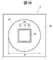
- FIG. 1B is a top view of the light emitting device according to the first embodiment of the present invention.
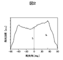
- FIG. 2 is a graph showing an example of a wide batwing-shaped light distribution characteristic.
- FIG. 3A is a vertical cross-sectional view showing the flow of the manufacturing process of the light emitting device according to the first embodiment of the present invention.
- FIG. 3B is a vertical cross-sectional view showing the flow of the manufacturing process of the light emitting device according to the first embodiment of the present invention.
- FIG. 3C is a vertical cross-sectional view showing the flow of the manufacturing process of the light emitting device according to the first embodiment of the present invention.
- FIG. 3A is a vertical sectional view of a light emitting device according to the first embodiment of the present invention.
- FIG. 1B is a top view of the light emitting device according to the first embodiment of the present invention.
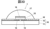
- FIG. 3D is a vertical cross-sectional view showing the flow of the manufacturing process of the light emitting device according to the first embodiment of the present invention.
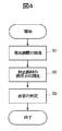
- FIG. 4 is a flowchart showing the flow of the manufacturing control process of the light emitting device according to the first embodiment of the present invention.
- FIG. 5 is a flowchart showing a flow of a process of acquiring a pass range of the diameter of the sealing member according to the first embodiment of the present invention.
- FIG. 6 is an example of a scatter plot in which the diameter of the lens resin is on the horizontal axis and the contact angle is on the vertical axis.
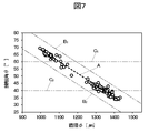
- FIG. 7 is a diagram in which two straight lines parallel to the regression line with the regression line as the center line are added to FIG. FIG.
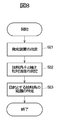
- FIG. 8 is a flowchart showing a flow of a step of acquiring a desired range of the contact angle of the sealing member according to the first embodiment of the present invention.
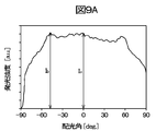
- FIG. 9A is an example of the light distribution characteristics of the light emitting device for obtaining a desired range of the contact angle.
- FIG. 9B is an example of the light distribution characteristics of the light emitting device for obtaining a desired range of the contact angle.
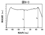
- FIG. 9C is an example of the light distribution characteristics of the light emitting device for obtaining a desired range of the contact angle.
- FIG. 10A is an example of the light distribution characteristics of the light emitting device for obtaining a desired range of the contact angle.
- FIG. 10B is an example of the light distribution characteristics of the light emitting device for obtaining a desired range of the contact angle.
- FIG. 11 is a flowchart showing a flow of a process of acquiring a pass range of the diameter of the sealing member according to the second embodiment of the present invention.
- FIG. 12 is an example of a scatter plot in which the diameter of the lens resin is on the horizontal axis and the relative strength on the axis is on the vertical axis.
- FIG. 13 is a diagram in which two straight lines parallel to the regression line with the regression line as the center line are added to FIG.
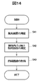
- FIG. 14 is a flowchart showing the flow of a process of acquiring a regression line for converting the measured value of the contact angle of the lens resin into the predicted value of the relative strength on the axis.
- the light emitting device 1 includes a substrate and 10, a light emitting element 13 with a DBR (Distributed Bragg Reflector) film 14 mounted on the substrate 10, a light reflecting film 16 provided on the surface of the substrate 10, and a bottom edge.
- a lens-shaped sealing member 17 for sealing the light emitting element 13 is provided on the substrate 10 so as to be in contact with the light reflecting film 16.
- the substrate 10 has a plate-shaped base material 11 and wiring 12 formed on the surface of the base material 11.
- the light emitting element 13 is connected to the wiring 12 by a conductive joining member 15 made of AuSn, solder, or the like.
- the light emitting element 13 is, for example, a light emitting diode (LED) having a chip substrate and a crystal layer including a light emitting layer provided on the chip substrate, and is, for example, an LED called a mini LED having a chip size of 100 to 200 ⁇ m. is there.
- the mounting form of the light emitting element 13 on the substrate 10 is not particularly limited, but is shown in FIGS. 1A and 1B rather than face-up mounting because it does not require a joining member such as a wire and does not hinder sealing at high speed. Flip chip mounting such as is preferable.
- the light emitting element 13 may be a light emitting element other than an LED such as a laser diode (LD).
- LD laser diode
- the DBR film 14 is provided on the opposite side (upper side in FIG. 1A) of the light emitting element 13 from the substrate 10.
- the DBR film 14 is made of, for example, a multilayer film of a dielectric such as SiO 2 and TiO 2 .
- the light emitted from the light emitting element 13 and taken out through the DBR film 14 has a peak of light emission intensity on the wide-angle side.
- the light reflecting film 16 is a member for reflecting light emitted from the light emitting element 13 toward the substrate 10, and the brightness of the light emitting device 1 can be improved by using the light reflecting film 16.
- the light reflecting film 16 is made of, for example, methyl silicone, dimethyl silicone, a silane fluoride coating material, an epoxy acrylate resist, or the like.
- the sealing member 17 is a drop-molded product formed by curing the dropped resin, and is formed without using a dam. Further, the sealing member 17 which is a drop-molded product has a lens shape whose surface is a convex curved surface, and functions as a lens that spreads the light distribution of the light emitted from the light emitting element 13. The planar shape of the sealing member 17 is circular, as shown in FIG. 1B.
- the sealing member 17 is made of a transparent resin that can be dropped, such as methylphenyl silicone, phenyl silicone, and organically modified silicone.
- the contact angle ⁇ of the sealing member 17 with the upper surface of the light reflecting film 16 depends on the material of the sealing member 17, the material of the light reflecting film 16 with which the edges of the sealing member 17 are in contact, and the like. Further, the contact angle ⁇ affects the light distribution characteristics of the light emitting device 1. For example, by combining the sealing member 17 having a contact angle ⁇ of 40 ° or more with the light emitting element 13 with the DBR film 14, a desired batwing-like wide light distribution characteristic can be obtained.
- the above-mentioned desired butt-wing-like wide light distribution characteristic is that the light emission has a peak between 0 and ⁇ 90 °, and the light emission intensity at the peak when the light distribution angle is 0 °.
- the emission characteristic is smaller than the intensity.
- the ratio of the emission intensity when the light distribution angle is 0 ° to the maximum emission intensity (hereinafter referred to as axial relative intensity) is 90. % Or less light distribution characteristics.
- the light distribution angle is an in-plane angle perpendicular to the substrate 10 including the axial direction with respect to the axial direction of the light emitting device 1 (upward direction in FIG. 1A).
- the sealing member 17 is formed from a resin having a thixotropic property such that the contact angle ⁇ of the sealing member 17 formed by the dropping method with the upper surface of the light reflecting film 16 becomes large, the sealing member 17 is formed.
- a protrusion is formed at the upper end of the light source to collect light on an axis having a light distribution angle of 0 °, and a batwing-like light distribution characteristic cannot be obtained. Therefore, the contact angle ⁇ is preferably 60 ° or less.
- the light emitting device 1 Since the light emitting device 1 has a wide light distribution characteristic like a bat wing, it is suitable for a direct type backlight used for, for example, a liquid crystal television. By using the light emitting device 1 as a light source, the uniformity of the brightness of the light emitting surface can be maintained even if the distance from the light emitting surface is reduced, so that the lighting device can be made thinner.
- FIG. 2 is a graph showing an example of a wide batwing-shaped light distribution characteristic.
- the emission intensity I a when the light distribution angle is 0 ° is about 76% of the maximum emission intensity I b , that is, the axial relative intensity is 76%.
- the on-axis relative intensity is a parameter used as an index of the quality of the batwing-shaped light distribution characteristic, and is judged to be a good characteristic when the on-axis relative intensity is smaller than a predetermined value (for example, 90%).
- a predetermined value for example, 90%
- the sealing member 17 may contain a filler made of SiO 2 or the like for scattering light, or particles of a phosphor.
- FIGS. 3A to 3D are vertical cross-sectional views showing the flow of the manufacturing process of the light emitting device 1 according to the first embodiment of the present invention.
- the light reflecting film 16 is formed on the substrate 10.
- the light reflecting film 16 is formed by screen printing or the like.
- the light emitting element 13 is mounted on the substrate 10. If there is no problem in forming the light reflecting film 16, the light emitting element 13 may be mounted before forming the light reflecting film 16.
- the sealing member 17 is formed.
- the sealing member 17 is formed by dropping the liquid resin 170, which is the material of the sealing member 17, onto the substrate 10 from the nozzle 20 of the dropping device and curing the liquid resin 170.
- the edge of the bottom surface of the sealing member 17 is in contact with the upper surface of the light reflecting film 16.
- FIG. 4 is a flowchart showing the flow of the manufacturing control process of the light emitting device 1 according to the first embodiment of the present invention.
- the light emitting device 1 which is the object of manufacturing control is manufactured by the above-mentioned method or the like (step S1).
- the diameter ⁇ of the sealing member 17 is measured (step S2).
- the diameter ⁇ of the sealing member 17 is measured, for example, by an image inspection using an image of the sealing member 17 taken from above.
- pass / fail is determined based on whether or not the diameter ⁇ of the sealing member 17 is within the pass range (step S3).
- the pass range is the range of the diameter ⁇ for obtaining the contact angle ⁇ of the sealing member 17 within the desired range, that is, the range of the diameter ⁇ corresponding to the desired range of the contact angle ⁇ of the sealing member 17. is there.
- step S3 The light emitting device 1 determined to pass in step S3 is treated as a passed product having desired light distribution characteristics.
- the light emitting device 1 determined to be unacceptable in step S3 is reshaped by removing the sealing member 17 by using, for example, a rework device. Then, steps S2 and S3 are performed again for the light emitting device 1 in which the sealing member 17 is reshaped.
- FIG. 5 is a flowchart showing a flow of a process for acquiring a pass range of the diameter ⁇ of the sealing member 17 according to the first embodiment of the present invention.
- lens resins a plurality of lens-shaped resins (hereinafter referred to as lens resins) are formed by drop molding using the same material as the sealing member 17 of the light emitting device 1, which is the object of manufacturing control (step S11). It is preferable that the discharge amount of the resin in the drop molding of the lens resin is set to the same amount as the discharge amount of the resin 170 in the drop molding of the sealing member 17.
- the lens resin can be formed by dropping the resin onto the flat plate-shaped base material.
- the diameter ⁇ and contact angle ⁇ of the lens resin change depending on the material of the base material on which the resin is dropped. Therefore, in order to obtain measured values in a wide range, it is preferable to drop-mold the lens resin on a plurality of base materials made of different materials.
- the diameter ⁇ and the contact angle ⁇ of each of the formed plurality of lens resins are measured (step S12).
- the diameter ⁇ of the sealing member 17 is measured, for example, by an image inspection using an image of the sealing member 17 taken from the side.
- the regression line A is obtained by regression analysis using the measured value of the diameter ⁇ of the lens resin and the measured value of the contact angle ⁇ as variables (step S13). This regression analysis is performed, for example, by the method of least squares.
- FIG. 6 is an example of a scatter plot in which the diameter ⁇ of the lens resin is the horizontal axis and the contact angle ⁇ is the vertical axis.
- FIG. 6 shows data points each having a measured value of the corresponding diameter ⁇ and a measured value of the contact angle ⁇ , and a regression line A obtained by their regression analysis.
- the coefficient of determination R 2 of the regression line A is 0.9853.
- the data points included in the region R 1 in FIG. 6 were obtained when a silane fluoride-based coating material was used as the base for the drop molding of the lens resin, and the data points included in the region R 2 were obtained. , Obtained when transparent dimethyl silicone was used as the base for the drop molding of the lens resin, and the data points included in region R 3 are white epoxy acrylate-based resists for the base for the drop molding of the lens resin. It was obtained when used.
- the pass range of the diameter ⁇ is obtained in consideration of the variation accuracy of the contact angle ⁇ (step S14).
- FIG. 7 is a diagram in which two straight lines B 1 and B 2 parallel to the regression line A with the regression line A as the center line are added to FIG.
- the straight lines B 1 and B 2 indicate the upper limit and the lower limit of the variation of the contact angle ⁇ of the lens resin on the regression line A, respectively, and the regression lines A and the straight lines B 1 and B 2 representing the variation accuracy of the contact angle ⁇ , respectively.
- the distance between the regression line A and the straight lines B 1 and B 2 calculated as 6 ⁇ in the vertical axis direction is 7.5 °.
- the desired range of the contact angle ⁇ is the range of the contact angle ⁇ for obtaining the desired light distribution characteristic, for example, the range of the contact angle ⁇ corresponding to the desired range of the axial relative strength. ..
- the desired range of the contact angle ⁇ is a range of 40 ° or more and 60 ° or less, and the upper limit and the lower limit thereof are shown by straight lines C 1 and C 2 , respectively.
- the pass range of the diameter ⁇ is the range of the diameter ⁇ in which the contact angle ⁇ falls within a desired range even when the variation in the contact angle ⁇ is taken into consideration.
- the upper limit of the pass range of the diameter ⁇ is 1250 ⁇ m, which is the diameter ⁇ at the intersection of the straight line B 2 and the straight line C 2
- the lower limit of the pass range of the diameter ⁇ is the straight line B 1 and the straight line C. It is 1190 ⁇ m, which is the diameter ⁇ at the intersection of 1 .
- step S14 Using the pass range of the diameter ⁇ acquired in step S14, it is possible to determine the pass / fail of the light emitting device 1 in step S3.
- FIG. 8 is a flowchart showing a flow of a process of acquiring a desired range of the contact angle ⁇ of the sealing member 17 according to the first embodiment of the present invention.
- a plurality of light emitting devices (hereinafter referred to as light emitting device Y) in which the light emitting element is sealed by a lens-shaped sealing member (hereinafter referred to as sealing member X) are prepared (step S21).
- the relationship between the contact angle of the sealing member and the axial relative strength of the light emitting device (the ratio of the light emitting intensity when the light distribution angle is 0 ° to the maximum light emitting intensity) hardly depends on the material of the sealing member.
- the material of the sealing member X may be different from the material of the sealing member 17.
- the contact angle ⁇ of the sealing member X and the axial relative strength are measured for each of the plurality of light emitting devices Y (step S22).
- the on-axis relative intensity is obtained by measuring the light distribution characteristic of the light emitting device Y.
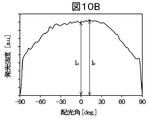
- FIG. 9A-9C, 10A, and 10B are examples of light distribution characteristics of the light emitting device Y for acquiring a desired range of the contact angle ⁇ .
- Figure 9A ⁇ Figure 9C, FIG. 10A, I a in FIG. 10B is a light emitting intensity when the light distribution angle is 0 °, I b is the maximum luminous intensity. Therefore, the ratio of I a to I b is the axial relative strength.
- the axial relative intensity in the light distribution characteristics shown in FIG. 9A is 99%. Further, the contact angle ⁇ of the sealing member X in the light emitting device Y having the light distribution characteristic shown in FIG. 9A was 64.2 °.
- the axial relative intensity in the light distribution characteristics shown in FIG. 9B is 76%. Further, the contact angle ⁇ of the sealing member X in the light emitting device Y having the light distribution characteristic shown in FIG. 9B was 56.2 °.
- the axial relative intensity in the light distribution characteristics shown in FIG. 9C is 87%. Further, the contact angle ⁇ of the sealing member X in the light emitting device Y having the light distribution characteristic shown in FIG. 9C was 47.1 °.
- the axial relative intensity in the light distribution characteristics shown in FIG. 10A is 91%. Further, the contact angle ⁇ of the sealing member X in the light emitting device Y having the light distribution characteristic shown in FIG. 10A was 35.6 °.
- the axial relative intensity in the light distribution characteristics shown in FIG. 10B is 98%. Further, the contact angle ⁇ of the sealing member X in the light emitting device Y having the light distribution characteristic shown in FIG. 10B was 27.6 °.
- the range of the contact angle ⁇ at which the axial relative strength of the target range can be obtained is specified from the contact angle ⁇ and the axial relative strength of the sealing members X obtained from the plurality of light emitting devices Y (step S23). ..
- the axial relative strength is 90%. It can be specified that the contact angle ⁇ for obtaining the following light distribution characteristics is in the range of about 40 ° or more and 60 ° or less. In this case, the range of 40 ° or more and 60 ° or less is set as the desired range of the contact angle ⁇ used in step S14.
- the light emitting device 1 which is the object of manufacturing control is manufactured by the above-mentioned method or the like (step S1).
- the diameter ⁇ of the sealing member 17 is measured (step S2).
- the diameter ⁇ of the sealing member 17 is measured, for example, by an image inspection.
- the pass range is a range of diameter ⁇ for obtaining the axial relative intensity of the light emitting device 1 within a desired range, that is, a range of diameter ⁇ corresponding to a desired range of the axial relative intensity of the light emitting device 1. is there.
- step S3 The light emitting device 1 determined to pass in step S3 is treated as a passed product having desired light distribution characteristics.
- the light emitting device 1 determined to be unacceptable in step S3 is reshaped by removing the sealing member 17 by using, for example, a rework device. Then, steps S2 and S3 are performed again for the light emitting device 1 in which the sealing member 17 is reshaped.
- FIG. 11 is a flowchart showing a flow of a process for acquiring a pass range of the diameter ⁇ of the sealing member 17 according to the second embodiment of the present invention.
- a plurality of lens resins are formed by drop molding using the same material as the sealing member 17 of the light emitting device 1, which is the object of manufacturing control (step S31).
- the diameter ⁇ and the contact angle ⁇ of each of the formed plurality of lens resins are measured (step S32).
- step S33 convert the measured value of the contact angle ⁇ of the lens resin into the predicted value of the axial relative intensity I r by using the regression line H to be described later.
- a regression straight line E (step S34). This regression analysis is performed, for example, by the method of least squares.
- the horizontal axis the diameter ⁇ of the lens resin is an example of a scatter diagram with the ordinate axis on the relative intensity I r.
- the scatter diagram of FIG. 12 is obtained by converting the measured value of the contact angle ⁇ of the scatter diagram of FIG. 6 into a predicted value of the axial relative strength.
- Figure 12 is a data points each having a predicted value of the measured value and the on-axis relative intensity I r of a corresponding diameter phi, regression line E obtained by their regression analysis are shown.
- the coefficient of determination R 2 of the regression line E is 0.9853.
- step S35 the desired range of the regression line E and the axial relative intensity I r, taking into account the variation accuracy of the axial relative intensity I r, to obtain the adequate range of the diameter phi.
- FIG. 13 is a diagram in which two straight lines F 1 and F 2 parallel to the regression line E having the regression line E as the center line are added to FIG.
- Straight F 1, F 2 are indicative of upper and lower limits of the variation of the predicted value of the axial relative intensity on each regression line E, the regression line E and the straight line F representing the variation accuracy of the axial relative intensity I r
- the distance in the vertical axis direction from 1 and F 2 is calculated as 6 ⁇ ( ⁇ is the standard deviation of the contact angle ⁇ ) based on, for example, the variation in the weight and volume of the lens resin and the relationship between the diameter ⁇ and the height. ..
- the distance between the regression line E and the straight lines F 1 and F 2 calculated as 6 ⁇ in the vertical axis direction is 4.7%.
- the desired range of axial relative intensity I r is the range of 90% or less, the upper limit is indicated by a straight line G.
- the adequate range of the diameter ⁇ is axial relative intensity I r even considering the variations of the axial relative intensity I r is in the range of diameter ⁇ falling within the desired range.
- the upper limit of the pass range of the diameter ⁇ is 1220 ⁇ m, which is the diameter ⁇ at the intersection of the straight line F 1 and the straight line G.
- step S35 Using the pass range of the diameter ⁇ acquired in step S35, it is possible to determine the pass / fail of the light emitting device 1 in step S3.
- step S33 a flow chart showing the flow of a process of obtaining the regression line H for converting the measured value of the contact angle ⁇ of the lens resin into the predicted value of the axial relative intensity I r.
- step S41 a plurality of light emitting devices Y in which the light emitting element is sealed by the lens-shaped sealing member X are prepared. Then, for each of a plurality of light emitting devices Y, measuring the contact angle ⁇ and the axial relative intensity I r of the sealing member X (step S42). These steps S41 and S42 are the same as steps S21 and S22 according to the first embodiment.
- a regression straight line H (step S43). This regression analysis is performed, for example, by the method of least squares.
- step S33 the lens resin converting the measured value of the contact angle ⁇ to the predicted value of the axial relative intensity I r.
- the prediction of the formula variables I r on the axis relative intensity I r of the regression line H at that time Obtained as a value.
- the contact angle of the sealing member and the axial relative strength of the light emitting device can be inspected by measuring the diameter of the sealing member. Since the diameter of the sealing member can be easily measured in a short time as compared with the measurement of the contact angle of the sealing member and the measurement of the light emitting characteristics of the light emitting device, the target is the light emitting device which is a controlled object. Whether or not it has light distribution characteristics can be easily determined in a short time.
- a method for manufacturing and controlling a light emitting device that can be used.
Landscapes
- Led Device Packages (AREA)
- Testing Of Optical Devices Or Fibers (AREA)
- Led Devices (AREA)
Abstract
発光素子13がレンズ形状の封止部材17により封止された発光装置1を製造する工程(S1)と、封止部材17の直径φを測定する工程(S2)と、直径φが、封止部材17の接触角θの所望の範囲に対応する合格範囲内にあるか否かにより、合否を判定する工程(S3)と、を含む、発光装置の製造管理方法を提供する。
Description
本発明は、発光装置の製造管理方法に関する。
従来、発光素子がレンズ形状の封止部材に封止された発光装置であって、光取り出し効率を向上させるために封止部材の接触角に制限を設けたものが知られている(例えば、特許文献1参照)。
特許文献1は、発光素子が搭載されたサブマウント上の封止部材の接触角が場所によって異なることにより、発光装置の光取り出し効率が向上すると記載している。
しかしながら、特許文献1の発光装置の製造管理においては、封止部材の接触角が場所によって異なっているかどうかの検査が必要であると考えられるが、個々の発光装置に対して封止部材の接触角を検査するには膨大な時間と労力が必要とされ、発光装置の生産効率を低下させる原因となる。また、一般的に、封止部材の接触角に特徴を有する発光装置の製造管理においては、封止部材の接触角の検査において同様の問題がある。
本発明の目的は、発光素子がレンズ形状の封止部材に封止された発光装置の製造管理方法であって、封止部材の接触角や接触角に依存する発光装置の配光特性を短時間で簡便に検査することのできる発光装置の製造管理方法を提供することにある。
本発明の一態様は、上記目的を達成するために、下記[1]~[10]の発光装置の製造管理方法を提供する。
[1]発光素子がレンズ形状の封止部材により封止された発光装置を製造する工程と、前記封止部材の直径を測定する工程と、前記直径が、前記封止部材の接触角の所望の範囲に対応する合格範囲内にあるか否かにより、合否を判定する工程と、を含む、発光装置の製造管理方法。
[2]前記合格範囲が、前記封止部材と同じ材料からなるレンズ形状の樹脂の直径の測定値と接触角の測定値を変数とする回帰分析により得られる回帰直線に基づいて得られる、上記[1]に記載の発光装置の製造管理方法。
[3]前記合格範囲が、前記回帰直線を中心線とする前記回帰直線に平行な2本の直線で表される、前記回帰直線上の前記樹脂の接触角のばらつきの上限と下限と、前記封止部材の接触角の前記所望の範囲の上限と下限から得られる、上記[2]に記載の発光装置の製造管理方法。
[4]前記所望の範囲が、40°以上、60°以下の範囲である、上記[1]~[3]のいずれか1項に記載の発光装置の製造管理方法。
[5]発光素子がレンズ形状の封止部材により封止された発光装置を製造する工程と、前記封止部材の直径を測定する工程と、前記直径が、前記発光装置の軸上相対強度の所望の範囲に対応する合格範囲内にあるか否かにより、合否を判定する工程と、を含み、前記発光装置の軸上相対強度が、前記発光装置の最大発光強度に対する配光角が0°のときの発光強度の割合である、発光装置の製造管理方法。
[6]前記合格範囲が、前記封止部材と同じ材料からなるレンズ形状の樹脂の直径の測定値と軸上相対強度の予測値を変数とする回帰分析により得られる第1の回帰直線に基づいて得られ、前記軸上相対強度の予測値が、第2の発光素子がレンズ形状の第2の封止部材により封止された第2の発光装置の軸上相対強度の測定値と第2の封止部材の接触角の測定値を変数とする回帰分析により得られる第2の回帰直線を用いて、前記樹脂の接触角の測定値を変換することにより得られ、前記第2の発光装置の軸上相対強度が、前記第2の発光装置の最大発光強度に対する配光角が0°のときの発光強度の割合である、上記[5]に記載の発光装置の製造管理方法。
[7]前記合格範囲が、前記第1の回帰直線を中心線とする前記第1の回帰直線に平行な2本の直線で表される、前記第1の回帰直線上の前記第2の発光装置の軸上相対強度のばらつきの上限と下限と、前記発光装置の軸上相対強度の前記所望の範囲の上限から得られる、上記[6]に記載の発光装置の製造管理方法。
[8]前記所望の範囲が、90%以下の範囲である、上記[5]~[7]のいずれか1項に記載の発光装置の製造管理方法。
[9]前記発光素子が、DBR膜付き発光素子である、上記[1]~[8]のいずれか1項に記載の発光装置の製造管理方法。
[10]前記発光素子が、光反射膜が表面上に設けられた基板上に実装され、前記封止部材が、底面の縁が前記光反射膜に接するように前記基板上に設けられ、前記光反射膜が、メチルシリコーン、ジメチルシリコーン、フッ化シラン系コーティング材、又はエポキシアクリレート系レジストからなり、前記封止部材が、メチルフェニルシリコーン、フェニルシリコーン、又は有機変性シリコーンからなる、上記[1]~[9]のいずれか1項に記載の発光装置の製造管理方法。
[2]前記合格範囲が、前記封止部材と同じ材料からなるレンズ形状の樹脂の直径の測定値と接触角の測定値を変数とする回帰分析により得られる回帰直線に基づいて得られる、上記[1]に記載の発光装置の製造管理方法。
[3]前記合格範囲が、前記回帰直線を中心線とする前記回帰直線に平行な2本の直線で表される、前記回帰直線上の前記樹脂の接触角のばらつきの上限と下限と、前記封止部材の接触角の前記所望の範囲の上限と下限から得られる、上記[2]に記載の発光装置の製造管理方法。
[4]前記所望の範囲が、40°以上、60°以下の範囲である、上記[1]~[3]のいずれか1項に記載の発光装置の製造管理方法。
[5]発光素子がレンズ形状の封止部材により封止された発光装置を製造する工程と、前記封止部材の直径を測定する工程と、前記直径が、前記発光装置の軸上相対強度の所望の範囲に対応する合格範囲内にあるか否かにより、合否を判定する工程と、を含み、前記発光装置の軸上相対強度が、前記発光装置の最大発光強度に対する配光角が0°のときの発光強度の割合である、発光装置の製造管理方法。
[6]前記合格範囲が、前記封止部材と同じ材料からなるレンズ形状の樹脂の直径の測定値と軸上相対強度の予測値を変数とする回帰分析により得られる第1の回帰直線に基づいて得られ、前記軸上相対強度の予測値が、第2の発光素子がレンズ形状の第2の封止部材により封止された第2の発光装置の軸上相対強度の測定値と第2の封止部材の接触角の測定値を変数とする回帰分析により得られる第2の回帰直線を用いて、前記樹脂の接触角の測定値を変換することにより得られ、前記第2の発光装置の軸上相対強度が、前記第2の発光装置の最大発光強度に対する配光角が0°のときの発光強度の割合である、上記[5]に記載の発光装置の製造管理方法。
[7]前記合格範囲が、前記第1の回帰直線を中心線とする前記第1の回帰直線に平行な2本の直線で表される、前記第1の回帰直線上の前記第2の発光装置の軸上相対強度のばらつきの上限と下限と、前記発光装置の軸上相対強度の前記所望の範囲の上限から得られる、上記[6]に記載の発光装置の製造管理方法。
[8]前記所望の範囲が、90%以下の範囲である、上記[5]~[7]のいずれか1項に記載の発光装置の製造管理方法。
[9]前記発光素子が、DBR膜付き発光素子である、上記[1]~[8]のいずれか1項に記載の発光装置の製造管理方法。
[10]前記発光素子が、光反射膜が表面上に設けられた基板上に実装され、前記封止部材が、底面の縁が前記光反射膜に接するように前記基板上に設けられ、前記光反射膜が、メチルシリコーン、ジメチルシリコーン、フッ化シラン系コーティング材、又はエポキシアクリレート系レジストからなり、前記封止部材が、メチルフェニルシリコーン、フェニルシリコーン、又は有機変性シリコーンからなる、上記[1]~[9]のいずれか1項に記載の発光装置の製造管理方法。
本発明によれば、発光素子がレンズ形状の封止部材に封止された発光装置の製造管理方法であって、封止部材の接触角や接触角に依存する発光装置の配光特性を短時間で簡便に検査することのできる発光装置の製造管理方法を提供することができる。
〔第1の実施の形態〕
まず、本実施の形態に係る発光装置の製造管理方法の対象物である発光装置1の構成例について説明する。
まず、本実施の形態に係る発光装置の製造管理方法の対象物である発光装置1の構成例について説明する。
(発光装置の構成)
図1Aと図1Bは、本発明の第1の実施の形態に係る発光装置1の垂直断面図と上面図である。発光装置1は、基板と10と、基板10上に実装された、DBR(Distributed Bragg Reflector)膜14付き発光素子13と、基板10の表面上に設けられた光反射膜16と、底面の縁が光反射膜16に接するように基板10上に設けられた、発光素子13を封止するレンズ形状の封止部材17とを備える。
図1Aと図1Bは、本発明の第1の実施の形態に係る発光装置1の垂直断面図と上面図である。発光装置1は、基板と10と、基板10上に実装された、DBR(Distributed Bragg Reflector)膜14付き発光素子13と、基板10の表面上に設けられた光反射膜16と、底面の縁が光反射膜16に接するように基板10上に設けられた、発光素子13を封止するレンズ形状の封止部材17とを備える。
基板10は、板状の基材11と、基材11の表面上に形成された配線12とを有する。発光素子13は、AuSnや半田などからなる導電性の接合部材15により配線12に接続されている。
発光素子13は、例えば、チップ基板と、チップ基板上に設けられた発光層を含む結晶層とを有する発光ダイオード(LED)であり、例えば、チップサイズが100~200μmのミニLEDと呼ばれるLEDである。発光素子13の基板10への実装形態は特に限定されないが、ワイヤーなどの接合部材を要せず、高速での封止を阻害しないため、フェイスアップ実装よりも、図1A、図1Bに示されるようなフリップチップ実装が好ましい。なお、発光素子13は、レーザーダイオード(LD)等のLED以外の発光素子であってもよい。
DBR膜14は、発光素子13の基板10と反対側(図1Aにおける上側)に設けられている。DBR膜14は、例えば、SiO2、TiO2等の誘電体の多層膜からなる。発光素子13から発せられてDBR膜14を介して取り出された光は、広角側に発光強度のピークを有する。
光反射膜16は、発光素子13から発せられて基板10側へ向かう光を反射するための部材であり、光反射膜16を用いることにより発光装置1の明るさを向上させることができる。光反射膜16は、例えば、メチルシリコーン、ジメチルシリコーン、フッ化シラン系コーティング材、エポキシアクリレート系レジストなどからなる。
封止部材17は、滴下した樹脂を硬化させることにより形成される滴下成形物であり、ダムを用いずに形成される。また、滴下成形物である封止部材17は、表面が凸状の曲面であるレンズ形状を有し、発光素子13から発せられた光の配光を広げるレンズとして機能する。封止部材17の平面形状は、図1Bに示されるように、円形である。封止部材17は、メチルフェニルシリコーン、フェニルシリコーン、有機変性シリコーンなどの滴下可能な透明樹脂からなる。
封止部材17の光反射膜16の上面との接触角θは、封止部材17の材料や、封止部材17の縁が接触する光反射膜16の材料などに依存する。また、接触角θは、発光装置1の配光特性に影響を与える。例えば、接触角θが40°以上の封止部材17をDBR膜14付き発光素子13と組み合わせることにより、所望のバットウィング状の広い配光特性が得ることができる。
ここで、上記の所望のバットウィング状の広い配光特性とは、0~±90°の配光角の間にピークを有し、配光角が0°のときの発光強度がピークの発光強度よりも小さい発光特性であり、例えば、配光角と発光強度の関係において、最大発光強度に対する配光角が0°のときの発光強度の割合(以下、軸上相対強度と呼ぶ)が90%以下である配光特性をいう。配光角は、発光装置1の軸方向(図1Aにおける上方向)を基準とした、軸方向を含む基板10に垂直な面内の角度である。
一方で、滴下法により形成される封止部材17の光反射膜16の上面との接触角θが大きくなるようなチクソトロピー性を有する樹脂から封止部材17が形成される場合、封止部材17の上端に突起が生じて配光角が0°の軸上に集光し、バットウィング状の配光特性が得られない場合がある。このため、接触角θは、60°以下であることが好ましい。
発光装置1は、バットウィング状の広い配光特性を有するため、例えば、液晶テレビなどに用いられる直下型バックライトに好適である。発光装置1を光源に用いることにより、発光面との距離を小さくしても、発光面の明るさの均一性を保つことができるため、照明装置を薄型化することができる。
図2は、バットウィング状の広い配光特性の一例を示すグラフである。図2に示される例では、配光角が0°のときの発光強度Iaが、最大発光強度Ibのおよそ76%、すなわち、軸上相対強度が76%となっている。軸上相対強度は、バットウィング状の配光特性の良し悪しの指標として用いられるパラメータであり、軸上相対強度が所定の値(例えば90%)よりも小さいときに良い特性であると判断される。
封止部材17は、光を散乱させるためのSiO2等からなるフィラーや、蛍光体の粒子を含んでもよい。
次に、本実施の形態に係る発光装置1の製造方法の一例について説明する。
(発光装置の製造方法)
図3A~図3Dは、本発明の第1の実施の形態に係る発光装置1の製造工程の流れを示す垂直断面図である。
図3A~図3Dは、本発明の第1の実施の形態に係る発光装置1の製造工程の流れを示す垂直断面図である。
まず、図3Aに示されるように、基板10上に光反射膜16を形成する。光反射膜16は、スクリーン印刷などにより形成される。
次に、図3Bに示されるように、基板10上に発光素子13を実装する。なお、光反射膜16の形成に支障がない場合は、光反射膜16を形成する前に発光素子13を実装してもよい。
次に、図3C、図3Dに示されるように、封止部材17を形成する。封止部材17の材料である液状の樹脂170を滴下装置のノズル20から基板10上に滴下し、これを硬化させることにより、封止部材17が形成される。封止部材17の底面の縁は、光反射膜16の上面に接する。
次に、本実施の形態に係る発光装置の製造管理方法の一例について説明する。
(発光装置の製造管理方法)
図4は、本発明の第1の実施の形態に係る発光装置1の製造管理工程の流れを示すフローチャートである。
図4は、本発明の第1の実施の形態に係る発光装置1の製造管理工程の流れを示すフローチャートである。
まず、製造管理の対象物である発光装置1を上述の方法などにより製造する(ステップS1)。
次に、封止部材17の直径φを測定する(ステップS2)。封止部材17の直径φは、例えば、封止部材17を上方から撮影した画像を用いる画像検査により測定される。
次に、封止部材17の直径φが合格範囲内にあるか否かにより、合否を判定する(ステップS3)。ここで、合格範囲は、所望の範囲内の封止部材17の接触角θを得るための直径φの範囲、すなわち封止部材17の接触角θの所望の範囲に対応した直径φの範囲である。
ステップS3において合格と判定された発光装置1は、所望の配光特性を有する合格品として扱われる。一方、ステップS3において不合格と判定された発光装置1は、例えば、リワーク装置を用いて封止部材17が除去され、再形成される。そして、封止部材17が再形成された発光装置1について、再びステップS2、ステップS3が実施される。
図5は、本発明の第1の実施の形態に係る封止部材17の直径φの合格範囲を取得する工程の流れを示すフローチャートである。
まず、製造管理の対象物である発光装置1の封止部材17と同じ材料を用いて、複数のレンズ形状の樹脂(以下、レンズ樹脂と呼ぶ)を滴下成形により形成する(ステップS11)。レンズ樹脂の滴下成形における樹脂の吐出量は、封止部材17の滴下成形における樹脂170の吐出量と同量に設定されることが好ましい。
なお、レンズ樹脂が発光素子を封止しているか否かは、レンズ樹脂の接触角にほとんど影響を与えないため、レンズ樹脂が発光素子を封止する必要はない。このため、例えば、平坦な板状の下地材の上に樹脂を滴下してレンズ樹脂を形成することができる。
レンズ樹脂の直径φや接触角θは、樹脂を滴下する下地材の材料によって変化する。このため、広い範囲での測定値を取得するために、異なる材質からなる複数の下地材の上にレンズ樹脂を滴下成形することが好ましい。
次に、形成した複数のレンズ樹脂の各々の直径φと接触角θを測定する(ステップS12)。封止部材17の直径φは、例えば、封止部材17を側方から撮影した画像を用いる画像検査により測定される。
次に、レンズ樹脂の直径φの測定値と接触角θの測定値を変数とする回帰分析により、回帰直線Aを求める(ステップS13)。この回帰分析は、例えば、最小二乗法により行われる。
ステップS13により得られる回帰直線Aは、レンズ樹脂の直径φと接触角θの関係を示す直線であり、θ=aφ+bという一次方程式で表される(aは回帰直線の傾き、bは切片)。
図6は、レンズ樹脂の直径φを横軸、接触角θを縦軸とする散布図の例である。図6には、対応する直径φの測定値と接触角θの測定値を各々が有するデータ点と、それらの回帰分析により得られた回帰直線Aが示されている。図6の回帰直線Aは、一次方程式θ=-0.0822φ+150.49で表される。回帰直線Aの決定係数R2は0.9853である。
なお、図6の領域R1に含まれるデータ点は、レンズ樹脂の滴下成形の下地にフッ化シラン系コーティング材を用いた場合に得られたものであり、領域R2に含まれるデータ点は、レンズ樹脂の滴下成形の下地に透明なジメチルシリコーンを用いた場合に得られたものであり、領域R3に含まれるデータ点は、レンズ樹脂の滴下成形の下地に白色のエポキシアクリレート系レジストを用いた場合に得られたものである。
次に、回帰直線Aと接触角θの所望の範囲から、接触角θのばらつき精度を考慮して、直径φの合格範囲を取得する(ステップS14)。
図7は、回帰直線Aを中心線とする回帰直線Aに平行な2本の直線B1、B2を図6に加えた図である。直線B1、B2は、それぞれ回帰直線A上のレンズ樹脂の接触角θのばらつきの上限と下限を示すものであり、接触角θのばらつき精度を表す回帰直線Aと直線B1、B2との縦軸方向の距離は、例えば、レンズ樹脂の重量と体積のばらつきや、直径φと高さの関係に基づいて6σ(σは接触角θの標準偏差)と算出される。図7に示される例では、6σとして算出される回帰直線Aと直線B1、B2の縦軸方向の距離は、7.5°である。
ここで、接触角θの所望の範囲とは、所望の配光特性を得るための接触角θの範囲であり、例えば、軸上相対強度の所望の範囲に対応した接触角θの範囲である。図7に示される例では、接触角θの所望の範囲は、40°以上、60°以下の範囲であり、その上限と下限がそれぞれ直線C1、C2で示されている。
直径φの合格範囲は、接触角θのばらつきを考慮しても接触角θが所望の範囲内に収まる直径φの範囲である。図7に示される例では、直径φの合格範囲の上限は、直線B2と直線C2の交点における直径φである1250μmであり、直径φの合格範囲の下限は、直線B1と直線C1の交点における直径φである1190μmである。
ステップS14で取得した直径φの合格範囲を用いて、ステップS3の発光装置1の合否の判定を行うことができる。
図8は、本発明の第1の実施の形態に係る封止部材17の接触角θの所望の範囲を取得する工程の流れを示すフローチャートである。
まず、発光素子がレンズ形状の封止部材(以下、封止部材Xと呼ぶ)により封止された、複数の発光装置(以下、発光装置Yと呼ぶ)を用意する(ステップS21)。
なお、封止部材の接触角と発光装置の軸上相対強度(最大発光強度に対する配光角が0°のときの発光強度の割合)との関係は、封止部材の材料にほとんど依存しないため、封止部材Xの材料は封止部材17の材料と異なっていてもよい。
次に、複数の発光装置Yの各々に対して、封止部材Xの接触角θと軸上相対強度を測定する(ステップS22)。軸上相対強度は、発光装置Yの配光特性を測定することにより得られる。
図9A~図9C、図10A、図10Bは、接触角θの所望の範囲を取得するための発光装置Yの配光特性の例である。図9A~図9C、図10A、図10BのIaは配光角が0°のときの発光強度であり、Ibは最大発光強度である。このため、IaのIbに対する割合が軸上相対強度である。
図9Aに示される配光特性における軸上相対強度は99%である。また、図9Aに示される配光特性を有する発光装置Yにおける封止部材Xの接触角θは64.2°であった。
図9Bに示される配光特性における軸上相対強度は76%である。また、図9Bに示される配光特性を有する発光装置Yにおける封止部材Xの接触角θは56.2°であった。
図9Cに示される配光特性における軸上相対強度は87%である。また、図9Cに示される配光特性を有する発光装置Yにおける封止部材Xの接触角θは47.1°であった。
図10Aに示される配光特性における軸上相対強度は91%である。また、図10Aに示される配光特性を有する発光装置Yにおける封止部材Xの接触角θは35.6°であった。
図10Bに示される配光特性における軸上相対強度は98%である。また、図10Bに示される配光特性を有する発光装置Yにおける封止部材Xの接触角θは27.6°であった。
次に、複数の発光装置Yから得られた封止部材Xの接触角θと軸上相対強度から、目的の範囲の軸上相対強度が得られる接触角θの範囲を特定する(ステップS23)。
図9A~図9C、図10A、図10Bに係るものを含む発光装置Yから得られる封止部材Xの接触角θと軸上相対強度の測定値からは、例えば、軸上相対強度が90%以下の配光特性を得るための接触角θがおよそ40°以上、60°以下の範囲にあると特定することができる。この場合、40°以上、60°以下の範囲を、ステップS14で用いる接触角θの所望の範囲とする。
〔第2の実施の形態〕
第2の実施の形態は、発光装置1の製造管理方法において、封止部材17の直径が、所望の範囲内の軸上相対強度を得るための合格範囲内にあるか否かにより、合否を判定する点において、第1の実施の形態と異なる。なお、製造管理の対象物である発光装置1の構成及びその製造方法など、第1の実施の形態と同様の点については、その説明を省略又は簡略化する。
第2の実施の形態は、発光装置1の製造管理方法において、封止部材17の直径が、所望の範囲内の軸上相対強度を得るための合格範囲内にあるか否かにより、合否を判定する点において、第1の実施の形態と異なる。なお、製造管理の対象物である発光装置1の構成及びその製造方法など、第1の実施の形態と同様の点については、その説明を省略又は簡略化する。
(発光装置の製造管理方法)
第1の実施の形態と同様に、図4のフローチャートを用いて発光装置の製造管理工程の流れを説明する。
第1の実施の形態と同様に、図4のフローチャートを用いて発光装置の製造管理工程の流れを説明する。
まず、製造管理の対象物である発光装置1を上述の方法などにより製造する(ステップS1)。
次に、封止部材17の直径φを測定する(ステップS2)。封止部材17の直径φは、例えば、画像検査により測定される。
次に、封止部材17の直径φが合格範囲内にあるか否かにより、合否を判定する(ステップS3)。ここで、合格範囲は、所望の範囲内の発光装置1の軸上相対強度を得るための直径φの範囲、すなわち発光装置1の軸上相対強度の所望の範囲に対応した直径φの範囲である。
ステップS3において合格と判定された発光装置1は、所望の配光特性を有する合格品として扱われる。一方、ステップS3において不合格と判定された発光装置1は、例えば、リワーク装置を用いて封止部材17が除去され、再形成される。そして、封止部材17が再形成された発光装置1について、再びステップS2、ステップS3が実施される。
図11は、本発明の第2の実施の形態に係る封止部材17の直径φの合格範囲を取得する工程の流れを示すフローチャートである。
まず、製造管理の対象物である発光装置1の封止部材17と同じ材料を用いて、複数のレンズ樹脂を滴下成形により形成する(ステップS31)。次に、形成した複数のレンズ樹脂の各々の直径φと接触角θを測定する(ステップS32)。これらステップS31、ステップS32は、第1の実施の形態に係るステップS11、ステップS12と同様である。
次に、後述する回帰直線Hを用いてレンズ樹脂の接触角θの測定値を軸上相対強度Irの予測値に変換する(ステップS33)。
次に、レンズ樹脂の直径φの測定値と軸上相対強度Irの予測値を変数とする回帰分析により、回帰直線Eを求める(ステップS34)。この回帰分析は、例えば、最小二乗法により行われる。
ステップS34により得られる回帰直線Eは、レンズ樹脂の直径φと軸上相対強度Irの関係を示す直線であり、Ir=aφ+bという一次方程式で表される(aは回帰直線の傾き、bは切片)。
図12は、レンズ樹脂の直径φを横軸、軸上相対強度Irを縦軸とする散布図の例である。図12の散布図は、図6の散布図の接触角θの測定値を軸上相対強度の予測値に変換したものである。図12には、対応する直径φの測定値と軸上相対強度Irの予測値を各々が有するデータ点と、それらの回帰分析により得られた回帰直線Eが示されている。図12の回帰直線Eは、一次方程式Ir=0.0513φ+22.596で表される。回帰直線Eの決定係数R2は0.9853である。
次に、回帰直線Eと軸上相対強度Irの所望の範囲から、軸上相対強度Irのばらつき精度を考慮して、直径φの合格範囲を取得する(ステップS35)。
図13は、回帰直線Eを中心線とする回帰直線Eに平行な2本の直線F1、F2を図12に加えた図である。直線F1、F2は、それぞれ回帰直線E上の軸上相対強度の予測値のばらつきの上限と下限を示すものであり、軸上相対強度Irのばらつき精度を表す回帰直線Eと直線F1、F2との縦軸方向の距離は、例えば、レンズ樹脂の重量と体積のばらつきや、直径φと高さの関係に基づいて6σ(σは接触角θの標準偏差)と算出される。図13に示される例では、6σとして算出される回帰直線Eと直線F1、F2の縦軸方向の距離は、4.7%である。
図13に示される例では、軸上相対強度Irの所望の範囲は、90%以下の範囲であり、その上限が直線Gで示されている。
直径φの合格範囲は、軸上相対強度Irのばらつきを考慮しても軸上相対強度Irが所望の範囲内に収まる直径φの範囲である。図13に示される例では、直径φの合格範囲の上限は、直線F1と直線Gの交点における直径φである1220μmである。
ステップS35で取得した直径φの合格範囲を用いて、ステップS3の発光装置1の合否の判定を行うことができる。
図14は、ステップS33で用いられる、レンズ樹脂の接触角θの測定値を軸上相対強度Irの予測値に変換するための回帰直線Hを取得する工程の流れを示すフローチャートである。
まず、発光素子がレンズ形状の封止部材Xにより封止された、複数の発光装置Yを用意する(ステップS41)。次に、複数の発光装置Yの各々に対して、封止部材Xの接触角θと軸上相対強度Irを測定する(ステップS42)。これらステップS41、ステップS42は、第1の実施の形態に係るステップS21、ステップS22と同様である。
次に、封止部材Xの接触角θの測定値と発光装置Yの軸上相対強度Irの測定値を変数とする回帰分析により、回帰直線Hを求める(ステップS43)。この回帰分析は、例えば、最小二乗法により行われる。
この封止部材Xの接触角θの測定値と発光装置Yの軸上相対強度Irの測定値を変数とする一次方程式で表される回帰直線Hを用いて、ステップS33において、レンズ樹脂の接触角θの測定値を軸上相対強度Irの予測値に変換する。具体的には、回帰直線Hの式の変数θにレンズ樹脂の接触角θの測定値を代入することにより、そのときの回帰直線Hの式の変数Irが軸上相対強度Irの予測値として得られる。
(実施の形態の効果)
上記実施の形態に係る発光装置の製造管理方法によれば、封止部材の直径を測定することにより、封止部材の接触角や発光装置の軸上相対強度を検査することができる。封止部材の直径の測定は、封止部材の接触角の測定や発光装置の発光特性の測定と比較して短時間で簡便に行うことができるため、管理対象物である発光装置が目的の配光特性を有するか否かを短時間で簡便に判定することができる。
上記実施の形態に係る発光装置の製造管理方法によれば、封止部材の直径を測定することにより、封止部材の接触角や発光装置の軸上相対強度を検査することができる。封止部材の直径の測定は、封止部材の接触角の測定や発光装置の発光特性の測定と比較して短時間で簡便に行うことができるため、管理対象物である発光装置が目的の配光特性を有するか否かを短時間で簡便に判定することができる。
以上、本発明の実施の形態を説明したが、本発明は、上記実施の形態に限定されず、発明の主旨を逸脱しない範囲内において種々変形実施が可能である。
また、上記に記載した実施の形態は特許請求の範囲に係る発明を限定するものではない。また、実施の形態の中で説明した特徴の組合せの全てが発明の課題を解決するための手段に必須であるとは限らない点に留意すべきである。
発光素子がレンズ形状の封止部材に封止された発光装置の製造管理方法であって、封止部材の接触角や接触角に依存する発光装置の配光特性を短時間で簡便に検査することのできる発光装置の製造管理方法を提供する。
1 発光装置
10 基板
13 発光素子
14 DBR膜
16 光反射膜
17 封止部材
10 基板
13 発光素子
14 DBR膜
16 光反射膜
17 封止部材
Claims (10)
- 発光素子がレンズ形状の封止部材により封止された発光装置を製造する工程と、
前記封止部材の直径を測定する工程と、
前記直径が、前記封止部材の接触角の所望の範囲に対応する合格範囲内にあるか否かにより、合否を判定する工程と、
を含む、発光装置の製造管理方法。 - 前記合格範囲が、前記封止部材と同じ材料からなるレンズ形状の樹脂の直径の測定値と接触角の測定値を変数とする回帰分析により得られる回帰直線に基づいて得られる、
請求項1に記載の発光装置の製造管理方法。 - 前記合格範囲が、前記回帰直線を中心線とする前記回帰直線に平行な2本の直線で表される、前記回帰直線上の前記樹脂の接触角のばらつきの上限と下限と、前記封止部材の接触角の前記所望の範囲の上限と下限から得られる、
請求項2に記載の発光装置の製造管理方法。 - 前記所望の範囲が、40°以上、60°以下の範囲である、
請求項1~3のいずれか1項に記載の発光装置の製造管理方法。 - 発光素子がレンズ形状の封止部材により封止された発光装置を製造する工程と、
前記封止部材の直径を測定する工程と、
前記直径が、前記発光装置の軸上相対強度の所望の範囲に対応する合格範囲内にあるか否かにより、合否を判定する工程と、
を含み、
前記発光装置の軸上相対強度が、前記発光装置の最大発光強度に対する配光角が0°のときの発光強度の割合である、
発光装置の製造管理方法。 - 前記合格範囲が、前記封止部材と同じ材料からなるレンズ形状の樹脂の直径の測定値と軸上相対強度の予測値を変数とする回帰分析により得られる第1の回帰直線に基づいて得られ、
前記軸上相対強度の予測値が、第2の発光素子がレンズ形状の第2の封止部材により封止された第2の発光装置の軸上相対強度の測定値と第2の封止部材の接触角の測定値を変数とする回帰分析により得られる第2の回帰直線を用いて、前記樹脂の接触角の測定値を変換することにより得られ、
前記第2の発光装置の軸上相対強度が、前記第2の発光装置の最大発光強度に対する配光角が0°のときの発光強度の割合である、
請求項5に記載の発光装置の製造管理方法。 - 前記合格範囲が、前記第1の回帰直線を中心線とする前記第1の回帰直線に平行な2本の直線で表される、前記第1の回帰直線上の前記第2の発光装置の軸上相対強度のばらつきの上限と下限と、前記発光装置の軸上相対強度の前記所望の範囲の上限から得られる、
請求項6に記載の発光装置の製造管理方法。 - 前記所望の範囲が、90%以下の範囲である、
請求項5~7のいずれか1項に記載の発光装置の製造管理方法。 - 前記発光素子が、DBR膜付き発光素子である、
請求項1~8のいずれか1項に記載の発光装置の製造管理方法。 - 前記発光素子が、光反射膜が表面上に設けられた基板上に実装され、
前記封止部材が、底面の縁が前記光反射膜に接するように前記基板上に設けられ、
前記光反射膜が、メチルシリコーン、ジメチルシリコーン、フッ化シラン系コーティング材、又はエポキシアクリレート系レジストからなり、
前記封止部材が、メチルフェニルシリコーン、フェニルシリコーン、又は有機変性シリコーンからなる、
請求項1~9のいずれか1項に記載の発光装置の製造管理方法。
Applications Claiming Priority (2)
| Application Number | Priority Date | Filing Date | Title |
|---|---|---|---|
| JP2019115442A JP7180552B2 (ja) | 2019-06-21 | 2019-06-21 | 発光装置の製造管理方法 |
| JP2019-115442 | 2019-06-21 |
Publications (1)
| Publication Number | Publication Date |
|---|---|
| WO2020255572A1 true WO2020255572A1 (ja) | 2020-12-24 |
Family
ID=73995125
Family Applications (1)
| Application Number | Title | Priority Date | Filing Date |
|---|---|---|---|
| PCT/JP2020/018426 Ceased WO2020255572A1 (ja) | 2019-06-21 | 2020-05-01 | 発光装置の製造管理方法 |
Country Status (2)
| Country | Link |
|---|---|
| JP (1) | JP7180552B2 (ja) |
| WO (1) | WO2020255572A1 (ja) |
Citations (8)
| Publication number | Priority date | Publication date | Assignee | Title |
|---|---|---|---|---|
| US20060244969A1 (en) * | 2005-04-07 | 2006-11-02 | Ryan Tom W | Apparatus and methods for scatterometry of optical devices |
| JP2013080799A (ja) * | 2011-10-03 | 2013-05-02 | Panasonic Corp | 封止材料検査装置および封止材料検査方法 |
| JP2014082284A (ja) * | 2012-10-15 | 2014-05-08 | Dow Corning Toray Co Ltd | 凸状硬化物及び基材を備える一体化物の製造方法 |
| JP2015045164A (ja) * | 2013-08-28 | 2015-03-12 | 株式会社奥村組 | 繊維補強コンクリートの打設管理方法 |
| JP2017073549A (ja) * | 2015-10-08 | 2017-04-13 | 日亜化学工業株式会社 | 発光装置、集積型発光装置および発光モジュール |
| JP2018040422A (ja) * | 2016-09-07 | 2018-03-15 | 株式会社Subaru | 無段変速機の制御装置 |
| US20180212106A1 (en) * | 2017-01-20 | 2018-07-26 | Lite-On Opto Technology (Changzhou) Co., Ltd. | Light-emitting package structure provided with predetermined view angle, light-emitting package module and method for forming the same |
| JP2019057559A (ja) * | 2017-09-20 | 2019-04-11 | 日亜化学工業株式会社 | 発光装置の検査方法 |
Family Cites Families (1)
| Publication number | Priority date | Publication date | Assignee | Title |
|---|---|---|---|---|
| JP5893916B2 (ja) | 2011-12-28 | 2016-03-23 | ミネベア株式会社 | 照明装置及びそれが備える配光制御部材の作製方法 |
-
2019
- 2019-06-21 JP JP2019115442A patent/JP7180552B2/ja active Active
-
2020
- 2020-05-01 WO PCT/JP2020/018426 patent/WO2020255572A1/ja not_active Ceased
Patent Citations (8)
| Publication number | Priority date | Publication date | Assignee | Title |
|---|---|---|---|---|
| US20060244969A1 (en) * | 2005-04-07 | 2006-11-02 | Ryan Tom W | Apparatus and methods for scatterometry of optical devices |
| JP2013080799A (ja) * | 2011-10-03 | 2013-05-02 | Panasonic Corp | 封止材料検査装置および封止材料検査方法 |
| JP2014082284A (ja) * | 2012-10-15 | 2014-05-08 | Dow Corning Toray Co Ltd | 凸状硬化物及び基材を備える一体化物の製造方法 |
| JP2015045164A (ja) * | 2013-08-28 | 2015-03-12 | 株式会社奥村組 | 繊維補強コンクリートの打設管理方法 |
| JP2017073549A (ja) * | 2015-10-08 | 2017-04-13 | 日亜化学工業株式会社 | 発光装置、集積型発光装置および発光モジュール |
| JP2018040422A (ja) * | 2016-09-07 | 2018-03-15 | 株式会社Subaru | 無段変速機の制御装置 |
| US20180212106A1 (en) * | 2017-01-20 | 2018-07-26 | Lite-On Opto Technology (Changzhou) Co., Ltd. | Light-emitting package structure provided with predetermined view angle, light-emitting package module and method for forming the same |
| JP2019057559A (ja) * | 2017-09-20 | 2019-04-11 | 日亜化学工業株式会社 | 発光装置の検査方法 |
Also Published As
| Publication number | Publication date |
|---|---|
| JP2021002582A (ja) | 2021-01-07 |
| JP7180552B2 (ja) | 2022-11-30 |
Similar Documents
| Publication | Publication Date | Title |
|---|---|---|
| JP4808244B2 (ja) | 半導体発光装置およびその製造方法 | |
| JP4891626B2 (ja) | 液晶表示装置 | |
| US20130285087A1 (en) | Light emitting device and manufacturing method thereof | |
| CN106684225A (zh) | 封装结构及其制法 | |
| JP2008172239A (ja) | Ledパッケージ | |
| WO2011016295A1 (ja) | 発光装置及び発光装置の製造方法 | |
| WO2008046583A1 (en) | Cover for optoelectronic components | |
| JP2019080065A (ja) | 発光装置 | |
| TWI787693B (zh) | 顯示基板及其製備方法、顯示裝置 | |
| US20220238761A1 (en) | Light-emitting device and method for manufacturing same | |
| US20230069298A1 (en) | Light emitting device | |
| EP2475017A2 (en) | LED Package with a lens | |
| KR101039424B1 (ko) | 반도체 패키지 | |
| JP7180552B2 (ja) | 発光装置の製造管理方法 | |
| JP2016146452A (ja) | Ledモジュール及びその製造方法 | |
| CN108682732B (zh) | Led封装结构及led芯片封装方法 | |
| JP5549519B2 (ja) | 発光モジュールおよびその設計方法 | |
| JP2020102512A (ja) | 封止部材の形成方法 | |
| JP6887255B2 (ja) | 発光装置及び発光装置を用いた撮像装置 | |
| JP2019050326A (ja) | プロジェクター用等の指向性を有するled光源装置 | |
| US10763407B2 (en) | Light emitting device | |
| CN224111582U (zh) | 白光led器件 | |
| JP2013182955A (ja) | 発光装置および発光装置の製造方法 | |
| JP2014011197A (ja) | 発光装置 | |
| US20240079539A1 (en) | Light emitting device |
Legal Events
| Date | Code | Title | Description |
|---|---|---|---|
| 121 | Ep: the epo has been informed by wipo that ep was designated in this application |
Ref document number: 20826695 Country of ref document: EP Kind code of ref document: A1 |
|
| NENP | Non-entry into the national phase |
Ref country code: DE |
|
| 122 | Ep: pct application non-entry in european phase |
Ref document number: 20826695 Country of ref document: EP Kind code of ref document: A1 |