WO2020255448A1 - 半導体記憶装置 - Google Patents
半導体記憶装置 Download PDFInfo
- Publication number
- WO2020255448A1 WO2020255448A1 PCT/JP2019/048379 JP2019048379W WO2020255448A1 WO 2020255448 A1 WO2020255448 A1 WO 2020255448A1 JP 2019048379 W JP2019048379 W JP 2019048379W WO 2020255448 A1 WO2020255448 A1 WO 2020255448A1
- Authority
- WO
- WIPO (PCT)
- Prior art keywords
- memory
- magnetic resistance
- resistance memory
- storage device
- logic unit
- Prior art date
- Legal status (The legal status is an assumption and is not a legal conclusion. Google has not performed a legal analysis and makes no representation as to the accuracy of the status listed.)
- Ceased
Links
Images


Classifications
-
- G—PHYSICS
- G11—INFORMATION STORAGE
- G11C—STATIC STORES
- G11C11/00—Digital stores characterised by the use of particular electric or magnetic storage elements; Storage elements therefor
- G11C11/005—Digital stores characterised by the use of particular electric or magnetic storage elements; Storage elements therefor comprising combined but independently operative RAM-ROM, RAM-PROM, RAM-EPROM cells
-
- G—PHYSICS
- G11—INFORMATION STORAGE
- G11C—STATIC STORES
- G11C11/00—Digital stores characterised by the use of particular electric or magnetic storage elements; Storage elements therefor
- G11C11/02—Digital stores characterised by the use of particular electric or magnetic storage elements; Storage elements therefor using magnetic elements
- G11C11/16—Digital stores characterised by the use of particular electric or magnetic storage elements; Storage elements therefor using magnetic elements using elements in which the storage effect is based on magnetic spin effect
-
- G—PHYSICS
- G11—INFORMATION STORAGE
- G11C—STATIC STORES
- G11C11/00—Digital stores characterised by the use of particular electric or magnetic storage elements; Storage elements therefor
- G11C11/02—Digital stores characterised by the use of particular electric or magnetic storage elements; Storage elements therefor using magnetic elements
- G11C11/16—Digital stores characterised by the use of particular electric or magnetic storage elements; Storage elements therefor using magnetic elements using elements in which the storage effect is based on magnetic spin effect
- G11C11/165—Auxiliary circuits
- G11C11/1673—Reading or sensing circuits or methods
-
- G—PHYSICS
- G11—INFORMATION STORAGE
- G11C—STATIC STORES
- G11C11/00—Digital stores characterised by the use of particular electric or magnetic storage elements; Storage elements therefor
- G11C11/02—Digital stores characterised by the use of particular electric or magnetic storage elements; Storage elements therefor using magnetic elements
- G11C11/16—Digital stores characterised by the use of particular electric or magnetic storage elements; Storage elements therefor using magnetic elements using elements in which the storage effect is based on magnetic spin effect
- G11C11/165—Auxiliary circuits
- G11C11/1675—Writing or programming circuits or methods
-
- G—PHYSICS
- G11—INFORMATION STORAGE
- G11C—STATIC STORES
- G11C11/00—Digital stores characterised by the use of particular electric or magnetic storage elements; Storage elements therefor
- G11C11/56—Digital stores characterised by the use of particular electric or magnetic storage elements; Storage elements therefor using storage elements with more than two stable states represented by steps, e.g. of voltage, current, phase, frequency
- G11C11/5607—Digital stores characterised by the use of particular electric or magnetic storage elements; Storage elements therefor using storage elements with more than two stable states represented by steps, e.g. of voltage, current, phase, frequency using magnetic storage elements
-
- H—ELECTRICITY
- H10—SEMICONDUCTOR DEVICES; ELECTRIC SOLID-STATE DEVICES NOT OTHERWISE PROVIDED FOR
- H10B—ELECTRONIC MEMORY DEVICES
- H10B61/00—Magnetic memory devices, e.g. magnetoresistive RAM [MRAM] devices
-
- H—ELECTRICITY
- H10—SEMICONDUCTOR DEVICES; ELECTRIC SOLID-STATE DEVICES NOT OTHERWISE PROVIDED FOR
- H10N—ELECTRIC SOLID-STATE DEVICES NOT OTHERWISE PROVIDED FOR
- H10N50/00—Galvanomagnetic devices
- H10N50/10—Magnetoresistive devices
Definitions
- the present invention relates to a semiconductor storage device.
- this memory controller includes a storage circuit (15) as a semiconductor storage device. Then, as described in paragraphs 0021 and 0022 of Patent Document 1, this memory controller (C) uses the storage circuit (15) as a work memory for storing working data, and performs replacement processing. It is configured to perform various processes such as restoration processing and restoration processing.
- volatile memory has been generally used for semiconductor storage devices (work memory and the like described above) in which data is rewritten relatively frequently, but this volatile memory can be rewritten as non-volatile.
- MRAM magnetoresistive memory
- the magnetoresistive memory due to the structure of the magnetoresistive memory, if an attempt is made to secure a large number of data rewritable times, the data retention period becomes short, so that the number of rewritable times that can be replaced with the volatile memory can be obtained.
- the retention period of infrequently rewritten data such as setting data tends to be shortened. As a result, it becomes necessary to load the setting data from another storage device when the device in which the semiconductor storage device is used starts up, which may increase the start-up time and increase the power consumption due to such processing. is there.
- the semiconductor storage device includes a first magnetic resistance memory and a second magnetic resistance memory, which are two types of magnetic resistance memories accessed by a target logic unit which is one logic unit, and the target logic unit.
- the first magnetic resistance memory and the second magnetic resistance memory are formed on one semiconductor chip, and the first magnetic resistance memory has a larger coercive force than the second magnetic resistance memory.
- the coercive force of the second magnetoresistive memory is relatively small to secure a large number of data rewritable times.
- the coercive force can be made relatively large to secure a long data retention period. That is, by using two types of magnetic resistance memories, a memory area formed by the second magnetic resistance memory and having a large number of data rewritable times and a first magnetic resistance memory are formed in the semiconductor storage device. , Two types of memory areas can be formed, one is a memory area having a long data retention period. Then, according to the above configuration, it is possible to realize a semiconductor chip in which the target logic unit can access such two types of memory areas.
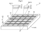
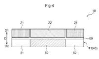
- Block diagram showing a schematic configuration of an example of a semiconductor chip Block diagram showing a schematic configuration of an example of a functional module Perspective view showing a schematic configuration of an example of a semiconductor storage device Diagram showing an example of the arrangement relationship between the semiconductor storage device and the target logic unit
- the semiconductor storage device 20 is a storage device formed on the semiconductor chip 1. Therefore, the semiconductor storage device 20 (for example, a memory cell constituting the semiconductor storage device 20 or a rewriting circuit for rewriting data to the memory cell) is formed by using a semiconductor material.
- FIG. 1 shows an example of a semiconductor chip 1 on which a semiconductor storage device 20 is formed.
- the semiconductor chip 1 is, for example, a SoC (System on a Chip).
- the semiconductor chip 1 includes a plurality of circuits (semiconductor integrated circuits) integrated on one chip.
- the semiconductor chip 1 is formed with a circuit constituting a logic unit 40 described later and a circuit constituting a semiconductor storage device 20 (memory unit).
- a circuit constituting another functional unit for example, an analog unit
- the plurality of circuits included in the semiconductor chip 1 are formed on a semiconductor substrate (semiconductor die such as a silicon die) incorporated in the semiconductor chip 1.
- the semiconductor chip 1 may include one semiconductor substrate, and all the circuits included in the semiconductor chip 1 may be formed on the one semiconductor substrate.
- the semiconductor chip 1 includes a plurality of functional modules 10 connected to each other by an internal bus 12. Further, the semiconductor chip 1 includes a processor 11 such as a CPU (Central Processing Unit), and the processor 11 is connected to each of the functional modules 10 by an internal bus 12.
- Each of the function modules 10 functions as a peripheral logic unit that realizes peripheral functions (support functions, etc.) of the processor 11, or has a semiconductor chip 1 and an external device 2 (a device provided outside the semiconductor chip 1). It functions as an interface unit for exchanging data or signals between them.
- the external device 2 is, for example, a storage device provided outside the semiconductor chip 1, a sensor, or the like.
- a part of the plurality of functional modules 10 is a functional module 10 for exchanging data or signals with the external device 2.
- Each of the function module 10 and the processor 11 includes a logic unit 40.
- the logic unit 40 includes a logic circuit (logic circuit), and performs processing (calculation processing, conversion processing, etc.) using the logic circuit.
- the semiconductor storage device 20 is a semiconductor storage device attached to the functional module 10, and is accessed by the logic unit 40 included in the functional module 10. That is, assuming that one logic unit 40 that accesses the semiconductor storage device 20 is the target logic unit 41, in the present embodiment, the target logic unit 41 is the logic unit 40 included in one functional module 10.
- the semiconductor storage device 20 functions as a register of the function module 10 including the target logic unit 41, and the target logic unit 41 (specifically, the arithmetic circuit 50 described later) is stored in the semiconductor storage device 20. It works based on the data that is being stored.
- FIG. 2 shows an example of the function module 10 including the target logic unit 41.
- the function module 10 other than the function module 10 shown in FIG. 2 will be referred to as another function module 10.
- the target logic unit 41 includes an arithmetic circuit 50 and a first circuit 51.
- the arithmetic circuit 50 is configured to perform arithmetic processing according to an operation program.
- the operation program for operating the arithmetic circuit 50 is stored in the semiconductor storage device 20 (specifically, the first magnetic resistance memory 21 described later).
- the first circuit 51 is connected to the internal bus 12 and the semiconductor storage device 20, and controls data transmission via the internal bus 12 between the semiconductor storage device 20 and the other functional module 10 or the processor 11. It is configured to do. That is, the first circuit 51 is a control circuit that functions as an internal bus control unit. An address bus for designating an address in the semiconductor storage device 20 and a data bus for exchanging data are formed between the first circuit 51 and the semiconductor storage device 20, and the first circuit 51 Is configured to read and write data at the specified address.
- the functional module 10 shown in FIG. 2 is a functional module that exchanges signals with the external device 2, and the target logic unit 41 includes a second circuit 52.
- the second circuit 52 is connected to the arithmetic circuit 50 and is also connected to the external device 2 via an external bus.
- the second circuit 52 is a control circuit that functions as an external signal control unit.
- the second circuit 52 is configured to convert the data input from the arithmetic circuit 50 into a signal and output it to the external device 2, and also converts the signal input from the external device 2 into data and the arithmetic circuit. It is configured to output to 50. It should be noted that the configuration may be such that only one of the output of the signal from the second circuit 52 to the external device 2 and the input of the signal from the external device 2 to the second circuit 52 is performed.
- the semiconductor storage device 20 includes a first magnetic resistance memory 21 and a second magnetic resistance memory 22, which are two types of magnetic resistance memories accessed by the target logic unit 41.
- Magnetoresistive Random Access Memory is a non-volatile memory having a magnetic tunnel junction as a memory cell 30.
- the second layer 32 which is an insulator layer, is combined with the first layer 31, which is two ferromagnetic layers. It has a structure sandwiched between the third layer 33 and the third layer 33.
- the ferromagnetic layer is formed using, for example, a ferromagnetic semiconductor material.
- One of the first layer 31 and the third layer 33 is a fixed layer in which the magnetization is fixed, and the other of the first layer 31 and the third layer 33 is a free layer in which the magnetization is variable.
- the memory cells 30 are arranged side by side in an array (two-dimensional array) on a plane orthogonal to the thickness direction D of the semiconductor chip 1. Although details are omitted, a rewriting circuit for rewriting data to the memory cells 30. Is configured to select a memory cell 30 to be rewritten by using a transistor (cell selection transistor).
- the target logic unit 41, the first magnetic resistance memory 21, and the second magnetic resistance memory 22 are formed on one semiconductor chip 1. That is, the first magnetic resistance memory 21 and the second magnetic resistance memory 22 are embedded MRAMs.
- the target logic unit 41, the first magnetic resistance memory 21, and the second magnetic resistance memory 22 are mixedly mounted on the same semiconductor substrate (semiconductor die).
- the first magnetic resistance memory 21 and the second magnetic resistance memory 22 are integrally formed on the front side D1 (surface layer side) with respect to the target logic unit 41.
- the target logic unit 41 is formed on the back side D2 (inner layer side) of the semiconductor chip 1 with respect to the first magnetic resistance memory 21 and the second magnetic resistance memory 22.
- the front side D1 is one side of the thickness direction D (the side where each element is formed with respect to the semiconductor substrate)
- the back side D2 is the other side of the thickness direction D (the side opposite to the front side D1). Is.
- the first magnetic resistance memory 21 has a larger coercive force than the second magnetic resistance memory 22.
- the coercive force of the memory cell 30 constituting the first magnetoresistive memory 21 is the coercive force of the memory cell 30 constituting the second magnetoresistive memory 22. Specifically, it is larger than the coercive force of the free layer).
- the first magnetic resistance memory 21 is configured by making the volume of the memory cells 30 constituting the first magnetic resistance memory 21 larger than the volume of the memory cells 30 constituting the second magnetic resistance memory 22.
- the coercive force of the memory cell 30 is made larger than the coercive force of the memory cell 30 constituting the second magnetoresistive memory 22.
- the volume of the memory cell 30 can be, for example, the total volume of each of the first layer 31, the second layer 32, and the third layer 33.
- the memory cell 30 constituting the first magnetic resistance memory 21 As an example of a configuration in which the volume of the memory cell 30 constituting the first magnetic resistance memory 21 is larger than the volume of the memory cell 30 constituting the second magnetic resistance memory 22, the memory cell 30 constituting the first magnetic resistance memory 21
- the area of (the area in the direction along the thickness direction D, the same applies hereinafter) can be larger than the area of the memory cells 30 constituting the second magnetoresistive memory 22.
- the thickness of the first layer 31, the thickness of the second layer 32, and the thickness of the third layer 33 should be the same between the first magnetoresistive memory 21 and the second magnetoresistive memory 22. Therefore, it is possible to suppress the complexity of the manufacturing process due to the formation of the two types of magnetoresistive memories on the semiconductor chip 1.
- the coercive force of the second magnetic resistance memory 22 is relatively small to reduce the number of times data can be rewritten.
- the first magnetoresistive memory 21 it is possible to secure a relatively large coercive force and secure a long data retention period while securing a large amount. That is, as a memory area accessible to the target logic unit 41, a memory area formed by the second magnetoresistive memory 22 and having a large number of data rewritable times and a data holding formed by the first magnetic resistance memory 21. It is possible to form two types of memory areas on the semiconductor chip 1, one is a memory area having a long period.
- the data required by the target logic unit 41 at the time of starting the device is the first magnetor from the viewpoint of shortening the start-up time of the device in which the semiconductor chip 1 is used. It is desirable that the configuration is stored in the resistance memory 21.
- the setting data is stored in the first magnetic resistance memory 21.
- the setting data stored in the first magnetic resistance memory 21 includes an operation program of the target logic unit 41 (specifically, the arithmetic circuit 50).
- the setting data stored in the first magnetic resistance memory 21 may include further data, for example, a configuration in which the initial setting data of the target logic unit 41 (specifically, the arithmetic circuit 50) is included.
- the data of constants (control constants and the like) used for the calculation in the target logic unit 41 can be included.
- the work data is stored in the second magnetic resistance memory 22.
- the work data stored in the second magnetic resistance memory 22 includes the calculation result by the target logic unit 41 (specifically, the calculation circuit 50).
- the work data stored in the second magnetic resistance memory 22 may include further data, for example, input data input to the target logic unit 41 (specifically, the arithmetic circuit 50). It can be configured or configured to include output data output from the target logic unit 41 (specifically, the arithmetic circuit 50).
- the second magnetoresistive memory 22 is arranged at a position closer to the arithmetic circuit 50 than the first magnetic resistance memory 21.
- the second magnetic resistance memory 22 is connected to the arithmetic circuit 50 as compared with the first magnetic resistance memory 21. Data is exchanged more frequently. Therefore, by arranging the second magnetoresistive memory 22 in which data is frequently exchanged with the arithmetic circuit 50 near the arithmetic circuit 50, the second magnetic resistance memory 22 is between the arithmetic circuit 50 and the second magnetic resistance memory 22.
- the wiring path length can be kept short. As a result, the length of the clock tree 60 for supplying the clock signal to each part can be kept short, and the power consumption can be reduced.
- the second magnetoresistive memory 22 is arranged at a position overlapping the arithmetic circuit 50 in a directional view along the thickness direction D, and at least a part of the first magnetic resistance memory 21 is viewed in the direction.
- the configuration is realized in which the second magnetoresistive memory 22 is arranged at a position closer to the arithmetic circuit 50 than the first magnetoresistive memory 21. be able to.
- the semiconductor storage device 20 is used as a register (register file) has been described as an example.
- the configuration is not limited to such a configuration, and the semiconductor storage device 20 may be used as a storage device other than the register.
- the semiconductor storage device 20 can be configured to be used as a cache for the processor 11.
- the target logic unit 41 is the logic unit 40 included in the processor 11.
- the tag (address) of the cached block is stored in the first magnetic resistance memory 21, and the contents of the cached block are stored in the second magnetic resistance memory 22.
- the first magnetoresistive memory 21 is a tag array (address array)
- the second magnetoresistive memory 22 is a data array.
- the processor 11 may be a GPU (Graphics Processing Unit) or the like in addition to the CPU.
- the semiconductor storage device 20 may be configured to be used as a storage device connected to the processor 11 via the internal bus 12.
- the target logic unit 41 is the logic unit 40 included in the processor 11.
- the memory area formed by the first magnetoresistive memory 21 is used as a program area
- the memory area formed by the second magnetic resistance memory 22 is used as a data area.
- the volume of the memory cell 30 constituting the first magnetic resistance memory 21 is made larger than the volume of the memory cell 30 constituting the second magnetic resistance memory 22, so that the first magnetic resistance is obtained.
- the configuration in which the coercive force of the memory 21 is made larger than the coercive force of the second magnetoresistive memory 22 has been described as an example. However, without being limited to such a configuration, if at least one of the structure and the material is different between the memory cell 30 constituting the first magnetoresistive memory 21 and the memory cell 30 constituting the second magnetoresistive memory 22.
- the coercive force of the first magnetoresistive memory 21 may be larger than the coercive force of the second magnetoresistive memory 22.
- the volume of the memory cell 30 constituting the first magnetic resistance memory 21 may be equal to or less than the volume of the memory cell 30 constituting the second magnetic resistance memory 22. ..
- the configuration in which the second magnetic resistance memory 22 is arranged at a position closer to the arithmetic circuit 50 than the first magnetic resistance memory 21 has been described as an example.
- the configuration is not limited to such a configuration, and for example, the first magnetic resistance memory 21 may be arranged at a position closer to the arithmetic circuit 50 than the second magnetic resistance memory 22.
- the semiconductor storage device (20) is a first magnetic resistance memory (21) and a second magnetic resistance memory, which are two types of magnetic resistance memories accessed by the target logic unit (41), which is one logic unit (40).
- the target logic unit (41), the first magnetic resistance memory (21), and the second magnetic resistance memory (22) are formed on one semiconductor chip (1), and the first magnetic resistance memory (21) is provided.
- the magnetic resistance memory (21) has a larger coercive force than the second magnetic resistance memory (22).
- the first magnetic resistance memory (21) has a larger coercive force than the second magnetic resistance memory (22). Therefore, the coercive force of the second magnetic resistance memory (22) is relatively small.
- the first magnetoresistive memory (21) it is possible to secure a long data retention period by relatively increasing the coercive force while securing a large number of times the data can be rewritten. That is, by using two types of magnetic resistance memories (21, 22), a memory area formed by the second magnetic resistance memory (22) in the semiconductor storage device (20) and having a large number of data rewritable times. And a memory area having a long data retention period formed by the first magnetoresistive memory (21), two types of memory areas can be formed. Then, according to the above configuration, it is possible to realize the semiconductor chip (1) in which the target logic unit (41) can access such two types of memory areas.
- the volume of the memory cell (30) constituting the first magnetoresistive memory (21) is larger than the volume of the memory cell (30) constituting the second magnetic resistance memory (22). ..
- the first magnetoresistive memory (21) and the second magnetoresistive memory (22) share the same structure and material, but the volume of the memory cell (30) is different.
- the coercive force of the resistance memory (21) can be made larger than the coercive force of the second magnetoresistive memory (22). Therefore, the manufacturing cost of the semiconductor chip (1) can be reduced as compared with the case where it is necessary to make the structure and the material different between the first magnetic resistance memory (21) and the second magnetic resistance memory (22). Can be done.
- the first magnetic resistance memory (21) stores setting data including the operation program of the target logic unit (41)
- the second magnetic resistance memory (22) stores the target logic unit (41). It is preferable that the work data including the calculation result by) is stored.
- the setting data is stored in the first magnetic resistance memory (21) having a long data retention period, so that the setting data is stored in the first magnetic resistance memory (21) when the device in which the semiconductor chip (1) is used is started.
- the need to write to 21) can be basically eliminated, the startup time can be shortened, and the power consumption required for such a writing process can be reduced.
- the life of the semiconductor storage device (20) is appropriately stored by storing the work data that is rewritten relatively frequently in the second magnetic resistance memory (22) that can be rewritten a large number of times. It can also be secured.
- the second magnetoresistive memory (22) can also retain the data for a certain period of time. Therefore, if work data is stored in the second magnetoresistive memory (22) when the device in which the semiconductor chip (1) is used is started, the start-up time can be further shortened by using the work data. You can also do it.
- the target logic unit (41) The second magnetoresistive memory (22) is closer to the arithmetic circuit (50) than the first magnetoresistive memory (21), and includes an arithmetic circuit (50) that performs arithmetic processing according to the operation program. It is preferable that it is arranged in.
- the second magnetic resistance memory is compared with the first magnetic resistance memory (21).
- data is exchanged with the arithmetic circuit (50) more frequently.
- the semiconductor storage device according to the present disclosure may be capable of exerting at least one of the above-mentioned effects.
Landscapes
- Engineering & Computer Science (AREA)
- Computer Hardware Design (AREA)
- Mram Or Spin Memory Techniques (AREA)
- Memory System (AREA)
- Semiconductor Memories (AREA)
- Hall/Mr Elements (AREA)
Abstract
Description
次に、半導体記憶装置のその他の実施形態について説明する。
以下、上記において説明した半導体記憶装置の概要について説明する。
20:半導体記憶装置
21:第1磁気抵抗メモリ
22:第2磁気抵抗メモリ
30:メモリセル
40:ロジック部
41:対象ロジック部
50:演算回路
Claims (4)
- 1つのロジック部である対象ロジック部によりアクセスされる2種類の磁気抵抗メモリである、第1磁気抵抗メモリと第2磁気抵抗メモリとを備え、
前記対象ロジック部と前記第1磁気抵抗メモリと前記第2磁気抵抗メモリとが1つの半導体チップに形成され、
前記第1磁気抵抗メモリは、前記第2磁気抵抗メモリよりも保磁力が大きい、半導体記憶装置。 - 前記第1磁気抵抗メモリを構成するメモリセルの体積が、前記第2磁気抵抗メモリを構成するメモリセルの体積よりも大きい、請求項1に記載の半導体記憶装置。
- 前記第1磁気抵抗メモリには、前記対象ロジック部の動作プログラムを含む設定データが記憶され、
前記第2磁気抵抗メモリには、前記対象ロジック部による演算結果を含むワークデータが記憶される、請求項1又は2に記載の半導体記憶装置。 - 前記対象ロジック部は、前記動作プログラムに従った演算処理を行う演算回路を備え、
前記第2磁気抵抗メモリは、前記第1磁気抵抗メモリよりも前記演算回路に近い位置に配置されている、請求項3に記載の半導体記憶装置。
Priority Applications (3)
| Application Number | Priority Date | Filing Date | Title |
|---|---|---|---|
| KR1020217040960A KR102578013B1 (ko) | 2019-06-17 | 2019-12-11 | 반도체 기억 장치 |
| US17/439,623 US12062388B2 (en) | 2019-06-17 | 2019-12-11 | Semiconductor storage device having magnetoresistive memories with a different coercive force |
| CN201980096069.XA CN113795935B (zh) | 2019-06-17 | 2019-12-11 | 半导体存储装置 |
Applications Claiming Priority (2)
| Application Number | Priority Date | Filing Date | Title |
|---|---|---|---|
| JP2019111966A JP7211273B2 (ja) | 2019-06-17 | 2019-06-17 | 半導体記憶装置 |
| JP2019-111966 | 2019-06-17 |
Publications (1)
| Publication Number | Publication Date |
|---|---|
| WO2020255448A1 true WO2020255448A1 (ja) | 2020-12-24 |
Family
ID=73838498
Family Applications (1)
| Application Number | Title | Priority Date | Filing Date |
|---|---|---|---|
| PCT/JP2019/048379 Ceased WO2020255448A1 (ja) | 2019-06-17 | 2019-12-11 | 半導体記憶装置 |
Country Status (5)
| Country | Link |
|---|---|
| US (1) | US12062388B2 (ja) |
| JP (1) | JP7211273B2 (ja) |
| KR (1) | KR102578013B1 (ja) |
| CN (1) | CN113795935B (ja) |
| WO (1) | WO2020255448A1 (ja) |
Families Citing this family (2)
| Publication number | Priority date | Publication date | Assignee | Title |
|---|---|---|---|---|
| JP7538085B2 (ja) | 2021-05-27 | 2024-08-21 | ルネサスエレクトロニクス株式会社 | 半導体装置 |
| TW202441505A (zh) | 2022-11-07 | 2024-10-16 | 日商索尼半導體解決方案公司 | 記憶裝置、電子機器及記憶裝置之控制方法 |
Citations (3)
| Publication number | Priority date | Publication date | Assignee | Title |
|---|---|---|---|---|
| JP2005101123A (ja) * | 2003-09-24 | 2005-04-14 | Sony Corp | 磁気記憶装置、磁気記憶装置の書き込み方法および磁気記憶装置の製造方法 |
| JP2012014787A (ja) * | 2010-06-30 | 2012-01-19 | Sony Corp | 記憶装置 |
| US20190066746A1 (en) * | 2017-08-28 | 2019-02-28 | Qualcomm Incorporated | VARYING ENERGY BARRIERS OF MAGNETIC TUNNEL JUNCTIONS (MTJs) IN DIFFERENT MAGNETO-RESISTIVE RANDOM ACCESS MEMORY (MRAM) ARRAYS IN A SEMICONDUCTOR DIE TO FACILITATE USE OF MRAM FOR DIFFERENT MEMORY APPLICATIONS |
Family Cites Families (10)
| Publication number | Priority date | Publication date | Assignee | Title |
|---|---|---|---|---|
| JP2002358777A (ja) * | 2001-05-30 | 2002-12-13 | Toshiba Corp | 半導体記憶装置及びそれを含む半導体装置 |
| JP2004363527A (ja) * | 2003-04-11 | 2004-12-24 | Toshiba Corp | 磁気記憶装置、データ複写装置、データ複写システム、データ複写プログラム、及びデータ複写方法 |
| JP2006135292A (ja) * | 2004-10-08 | 2006-05-25 | Toshiba Corp | 磁気抵抗効果素子 |
| JP5488833B2 (ja) * | 2008-03-07 | 2014-05-14 | 日本電気株式会社 | Mram混載システム |
| JP2010124373A (ja) * | 2008-11-21 | 2010-06-03 | Renesas Technology Corp | 半導体装置 |
| JP4745414B2 (ja) * | 2009-03-30 | 2011-08-10 | 株式会社東芝 | 磁気抵抗素子及び磁気メモリ |
| JP5472832B2 (ja) * | 2009-09-28 | 2014-04-16 | 日本電気株式会社 | 磁気メモリ |
| KR20130008929A (ko) * | 2011-07-13 | 2013-01-23 | 에스케이하이닉스 주식회사 | 개선된 자성층의 두께 마진을 갖는 자기 메모리 디바이스 |
| US9437272B1 (en) * | 2015-03-11 | 2016-09-06 | Qualcomm Incorporated | Multi-bit spin torque transfer magnetoresistive random access memory with sub-arrays |
| JP6414497B2 (ja) | 2015-03-25 | 2018-10-31 | アイシン・エィ・ダブリュ株式会社 | メモリコントローラ |
-
2019
- 2019-06-17 JP JP2019111966A patent/JP7211273B2/ja active Active
- 2019-12-11 CN CN201980096069.XA patent/CN113795935B/zh active Active
- 2019-12-11 KR KR1020217040960A patent/KR102578013B1/ko active Active
- 2019-12-11 WO PCT/JP2019/048379 patent/WO2020255448A1/ja not_active Ceased
- 2019-12-11 US US17/439,623 patent/US12062388B2/en active Active
Patent Citations (3)
| Publication number | Priority date | Publication date | Assignee | Title |
|---|---|---|---|---|
| JP2005101123A (ja) * | 2003-09-24 | 2005-04-14 | Sony Corp | 磁気記憶装置、磁気記憶装置の書き込み方法および磁気記憶装置の製造方法 |
| JP2012014787A (ja) * | 2010-06-30 | 2012-01-19 | Sony Corp | 記憶装置 |
| US20190066746A1 (en) * | 2017-08-28 | 2019-02-28 | Qualcomm Incorporated | VARYING ENERGY BARRIERS OF MAGNETIC TUNNEL JUNCTIONS (MTJs) IN DIFFERENT MAGNETO-RESISTIVE RANDOM ACCESS MEMORY (MRAM) ARRAYS IN A SEMICONDUCTOR DIE TO FACILITATE USE OF MRAM FOR DIFFERENT MEMORY APPLICATIONS |
Also Published As
| Publication number | Publication date |
|---|---|
| JP7211273B2 (ja) | 2023-01-24 |
| KR20220008327A (ko) | 2022-01-20 |
| JP2020205329A (ja) | 2020-12-24 |
| CN113795935A (zh) | 2021-12-14 |
| US12062388B2 (en) | 2024-08-13 |
| KR102578013B1 (ko) | 2023-09-14 |
| CN113795935B (zh) | 2025-09-12 |
| US20220157362A1 (en) | 2022-05-19 |
Similar Documents
| Publication | Publication Date | Title |
|---|---|---|
| KR100506062B1 (ko) | 복합형 메모리 장치 | |
| US9953702B2 (en) | Semiconductor memory devices, memory systems including the same and methods of operating the same | |
| US7023726B1 (en) | Hybrid magnetoresistive random access memory (MRAM) architecture | |
| EP1094467A2 (en) | Processing equipment with embedded MRAMS including dual read ports | |
| KR20170062614A (ko) | 상대 주소를 사용하는 메모리 장치의 접근 방법 | |
| US12062388B2 (en) | Semiconductor storage device having magnetoresistive memories with a different coercive force | |
| US20250329350A1 (en) | Centralized placement of command and address signals in devices and systems | |
| JPH11306750A (ja) | 磁気型半導体集積記憶装置 | |
| US20140098599A1 (en) | Semiconductor memory device with data path option function | |
| JP2005050337A (ja) | 不揮発性メモリ並列プロセッサ | |
| JP2004200641A (ja) | Nand型磁気抵抗ラム | |
| KR20140044121A (ko) | 멀티 인터페이스를 갖는 멀티포트 반도체 메모리 장치 | |
| US7652920B2 (en) | Semiconductor integrated circuit device | |
| US9946466B2 (en) | Mobile electronic device including embedded memory | |
| US20230005514A1 (en) | Command and address interface regions, and associated devices and systems | |
| US10847198B2 (en) | Memory system utilizing heterogeneous magnetic tunnel junction types in a single chip | |
| US7206221B2 (en) | Upside-down magnetoresistive random access memory | |
| JP4879172B2 (ja) | 半導体記憶装置、及びそれを搭載した半導体集積回路 | |
| JP2009049354A (ja) | 磁性装置を備えた集積回路チップ | |
| JP2005190312A (ja) | マルチチップパッケージ型メモリシステムおよびコンピュータシステム | |
| JP7756993B1 (ja) | 不揮発集積回路 |
Legal Events
| Date | Code | Title | Description |
|---|---|---|---|
| 121 | Ep: the epo has been informed by wipo that ep was designated in this application |
Ref document number: 19933624 Country of ref document: EP Kind code of ref document: A1 |
|
| ENP | Entry into the national phase |
Ref document number: 20217040960 Country of ref document: KR Kind code of ref document: A |
|
| NENP | Non-entry into the national phase |
Ref country code: DE |
|
| 122 | Ep: pct application non-entry in european phase |
Ref document number: 19933624 Country of ref document: EP Kind code of ref document: A1 |
|
| WWG | Wipo information: grant in national office |
Ref document number: 201980096069.X Country of ref document: CN |