WO2020255248A1 - 液晶素子 - Google Patents
液晶素子 Download PDFInfo
- Publication number
- WO2020255248A1 WO2020255248A1 PCT/JP2019/024083 JP2019024083W WO2020255248A1 WO 2020255248 A1 WO2020255248 A1 WO 2020255248A1 JP 2019024083 W JP2019024083 W JP 2019024083W WO 2020255248 A1 WO2020255248 A1 WO 2020255248A1
- Authority
- WO
- WIPO (PCT)
- Prior art keywords
- liquid crystal
- retardation
- wall portion
- electrode
- crystal element
- Prior art date
- Legal status (The legal status is an assumption and is not a legal conclusion. Google has not performed a legal analysis and makes no representation as to the accuracy of the status listed.)
- Ceased
Links
Images









Classifications
-
- G—PHYSICS
- G02—OPTICS
- G02F—OPTICAL DEVICES OR ARRANGEMENTS FOR THE CONTROL OF LIGHT BY MODIFICATION OF THE OPTICAL PROPERTIES OF THE MEDIA OF THE ELEMENTS INVOLVED THEREIN; NON-LINEAR OPTICS; FREQUENCY-CHANGING OF LIGHT; OPTICAL LOGIC ELEMENTS; OPTICAL ANALOGUE/DIGITAL CONVERTERS
- G02F1/00—Devices or arrangements for the control of the intensity, colour, phase, polarisation or direction of light arriving from an independent light source, e.g. switching, gating or modulating; Non-linear optics
- G02F1/01—Devices or arrangements for the control of the intensity, colour, phase, polarisation or direction of light arriving from an independent light source, e.g. switching, gating or modulating; Non-linear optics for the control of the intensity, phase, polarisation or colour
- G02F1/13—Devices or arrangements for the control of the intensity, colour, phase, polarisation or direction of light arriving from an independent light source, e.g. switching, gating or modulating; Non-linear optics for the control of the intensity, phase, polarisation or colour based on liquid crystals, e.g. single liquid crystal display cells
- G02F1/133—Constructional arrangements; Operation of liquid crystal cells; Circuit arrangements
- G02F1/1333—Constructional arrangements; Manufacturing methods
- G02F1/1343—Electrodes
- G02F1/134309—Electrodes characterised by their geometrical arrangement
- G02F1/134381—Hybrid switching mode, i.e. for applying an electric field with components parallel and orthogonal to the substrates
-
- G—PHYSICS
- G02—OPTICS
- G02F—OPTICAL DEVICES OR ARRANGEMENTS FOR THE CONTROL OF LIGHT BY MODIFICATION OF THE OPTICAL PROPERTIES OF THE MEDIA OF THE ELEMENTS INVOLVED THEREIN; NON-LINEAR OPTICS; FREQUENCY-CHANGING OF LIGHT; OPTICAL LOGIC ELEMENTS; OPTICAL ANALOGUE/DIGITAL CONVERTERS
- G02F1/00—Devices or arrangements for the control of the intensity, colour, phase, polarisation or direction of light arriving from an independent light source, e.g. switching, gating or modulating; Non-linear optics
- G02F1/01—Devices or arrangements for the control of the intensity, colour, phase, polarisation or direction of light arriving from an independent light source, e.g. switching, gating or modulating; Non-linear optics for the control of the intensity, phase, polarisation or colour
- G02F1/13—Devices or arrangements for the control of the intensity, colour, phase, polarisation or direction of light arriving from an independent light source, e.g. switching, gating or modulating; Non-linear optics for the control of the intensity, phase, polarisation or colour based on liquid crystals, e.g. single liquid crystal display cells
- G02F1/133—Constructional arrangements; Operation of liquid crystal cells; Circuit arrangements
- G02F1/1333—Constructional arrangements; Manufacturing methods
- G02F1/1339—Gaskets; Spacers; Sealing of cells
- G02F1/13394—Gaskets; Spacers; Sealing of cells spacers regularly patterned on the cell subtrate, e.g. walls, pillars
-
- G—PHYSICS
- G02—OPTICS
- G02F—OPTICAL DEVICES OR ARRANGEMENTS FOR THE CONTROL OF LIGHT BY MODIFICATION OF THE OPTICAL PROPERTIES OF THE MEDIA OF THE ELEMENTS INVOLVED THEREIN; NON-LINEAR OPTICS; FREQUENCY-CHANGING OF LIGHT; OPTICAL LOGIC ELEMENTS; OPTICAL ANALOGUE/DIGITAL CONVERTERS
- G02F1/00—Devices or arrangements for the control of the intensity, colour, phase, polarisation or direction of light arriving from an independent light source, e.g. switching, gating or modulating; Non-linear optics
- G02F1/01—Devices or arrangements for the control of the intensity, colour, phase, polarisation or direction of light arriving from an independent light source, e.g. switching, gating or modulating; Non-linear optics for the control of the intensity, phase, polarisation or colour
- G02F1/13—Devices or arrangements for the control of the intensity, colour, phase, polarisation or direction of light arriving from an independent light source, e.g. switching, gating or modulating; Non-linear optics for the control of the intensity, phase, polarisation or colour based on liquid crystals, e.g. single liquid crystal display cells
- G02F1/133—Constructional arrangements; Operation of liquid crystal cells; Circuit arrangements
- G02F1/1333—Constructional arrangements; Manufacturing methods
- G02F1/133377—Cells with plural compartments or having plurality of liquid crystal microcells partitioned by walls, e.g. one microcell per pixel
-
- G—PHYSICS
- G02—OPTICS
- G02F—OPTICAL DEVICES OR ARRANGEMENTS FOR THE CONTROL OF LIGHT BY MODIFICATION OF THE OPTICAL PROPERTIES OF THE MEDIA OF THE ELEMENTS INVOLVED THEREIN; NON-LINEAR OPTICS; FREQUENCY-CHANGING OF LIGHT; OPTICAL LOGIC ELEMENTS; OPTICAL ANALOGUE/DIGITAL CONVERTERS
- G02F1/00—Devices or arrangements for the control of the intensity, colour, phase, polarisation or direction of light arriving from an independent light source, e.g. switching, gating or modulating; Non-linear optics
- G02F1/01—Devices or arrangements for the control of the intensity, colour, phase, polarisation or direction of light arriving from an independent light source, e.g. switching, gating or modulating; Non-linear optics for the control of the intensity, phase, polarisation or colour
- G02F1/13—Devices or arrangements for the control of the intensity, colour, phase, polarisation or direction of light arriving from an independent light source, e.g. switching, gating or modulating; Non-linear optics for the control of the intensity, phase, polarisation or colour based on liquid crystals, e.g. single liquid crystal display cells
- G02F1/133—Constructional arrangements; Operation of liquid crystal cells; Circuit arrangements
- G02F1/1333—Constructional arrangements; Manufacturing methods
- G02F1/1337—Surface-induced orientation of the liquid crystal molecules, e.g. by alignment layers
-
- G—PHYSICS
- G02—OPTICS
- G02F—OPTICAL DEVICES OR ARRANGEMENTS FOR THE CONTROL OF LIGHT BY MODIFICATION OF THE OPTICAL PROPERTIES OF THE MEDIA OF THE ELEMENTS INVOLVED THEREIN; NON-LINEAR OPTICS; FREQUENCY-CHANGING OF LIGHT; OPTICAL LOGIC ELEMENTS; OPTICAL ANALOGUE/DIGITAL CONVERTERS
- G02F1/00—Devices or arrangements for the control of the intensity, colour, phase, polarisation or direction of light arriving from an independent light source, e.g. switching, gating or modulating; Non-linear optics
- G02F1/01—Devices or arrangements for the control of the intensity, colour, phase, polarisation or direction of light arriving from an independent light source, e.g. switching, gating or modulating; Non-linear optics for the control of the intensity, phase, polarisation or colour
- G02F1/13—Devices or arrangements for the control of the intensity, colour, phase, polarisation or direction of light arriving from an independent light source, e.g. switching, gating or modulating; Non-linear optics for the control of the intensity, phase, polarisation or colour based on liquid crystals, e.g. single liquid crystal display cells
- G02F1/133—Constructional arrangements; Operation of liquid crystal cells; Circuit arrangements
- G02F1/1333—Constructional arrangements; Manufacturing methods
- G02F1/1339—Gaskets; Spacers; Sealing of cells
- G02F1/13398—Spacer materials; Spacer properties
-
- G—PHYSICS
- G02—OPTICS
- G02F—OPTICAL DEVICES OR ARRANGEMENTS FOR THE CONTROL OF LIGHT BY MODIFICATION OF THE OPTICAL PROPERTIES OF THE MEDIA OF THE ELEMENTS INVOLVED THEREIN; NON-LINEAR OPTICS; FREQUENCY-CHANGING OF LIGHT; OPTICAL LOGIC ELEMENTS; OPTICAL ANALOGUE/DIGITAL CONVERTERS
- G02F1/00—Devices or arrangements for the control of the intensity, colour, phase, polarisation or direction of light arriving from an independent light source, e.g. switching, gating or modulating; Non-linear optics
- G02F1/29—Devices or arrangements for the control of the intensity, colour, phase, polarisation or direction of light arriving from an independent light source, e.g. switching, gating or modulating; Non-linear optics for the control of the position or the direction of light beams, i.e. deflection
- G02F1/294—Variable focal length devices
Definitions
- the present invention relates to a liquid crystal element.
- the liquid crystal lens array described in Patent Document 1 includes a pattern electrode layer, a ground electrode layer, a liquid crystal layer, and an upright portion.
- the pattern electrode layer is composed of a first pattern electrode layer and a second pattern electrode layer.
- the erection portion projects from the substrate having the ground electrode layer toward the inside of the liquid crystal layer toward the pattern electrode layer.
- the erection part has conductivity.
- the surface of the upright portion is a weak anchoring surface.
- the weak anchoring surface is a surface having a weaker binding force (alignment regulating force) with respect to liquid crystal molecules than the surface of the alignment film constituting the liquid crystal layer.
- the influence of the electric field leaking from the electrode on the high potential side is shielded by the vertical portion, so that the potential of the electrode on the low potential side does not increase effectively. Therefore, the maximum value of the optical phase difference increases, the deflection angle increases, and the optical phase difference (corresponding to retardation) becomes close to a straight line.
- the relationship between the upright portion and the optical phase difference is not clear. For example, if the minimum value of the optical phase difference is located corresponding to one of the standing portions adjacent to each other, and the maximum value of the optical phase difference is located corresponding to the other standing portion. Can be considered.
- the inventor of the present application responded to a narrow unit electrode when the width of the unit electrode composed of the first electrode and the second electrode was narrowed in a liquid crystal element having a wavy attenuation. , Found that the amplitude difference of the wavy retardation is attenuated.
- An object of the present invention is to provide a liquid crystal element capable of suppressing attenuation of the amplitude difference of wavy retardation.
- the liquid crystal element includes a plurality of unit electrodes, a liquid crystal layer, and a plurality of wall portions.
- Each of the plurality of unit electrodes includes a first electrode and a second electrode.
- a voltage is applied to the liquid crystal layer from each of the plurality of unit electrodes.
- the plurality of wall portions are arranged on the liquid crystal layer.
- the liquid crystal layer has a wavy retardation. Two or more peaks of the plurality of retardation peaks correspond to the positions of the plurality of wall portions, respectively.
- the wall surface of the wall portion is preferably composed of a polymer, a substance having a polar portion, or a polymer having a polar moiety.
- the director of the liquid crystal molecules in contact with the wall portion preferably faces the direction along the interface of the liquid crystal layer.
- the anchoring energy of the wall portion is preferably 1 ⁇ 10 -6 (J / m 2 ) or more.
- the wall portion faces the region between the first electrode and the second electrode constituting the unit electrode.
- the wall portion faces the region between the unit electrode and the unit electrode.
- the wall portion faces either the first electrode or the second electrode.
- the wall portion extends from one interface side of the liquid crystal layer to the other interface side.
- the plurality of unit electrodes are arranged concentrically with respect to the optical axis.
- the width of the plurality of unit electrodes is preferably smaller than that of the unit electrodes located outside the radial direction with respect to the optical axis.
- the wall portion is arranged corresponding to the unit electrode located outside the predetermined position in the radial direction among the plurality of unit electrodes.
- liquid crystal element capable of suppressing attenuation of the amplitude difference of wavy retardation.
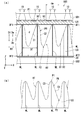
- FIG. 1A is a diagram showing a state (pre-twist angle: 45 degrees) of liquid crystal molecules in contact with the wall portion of the liquid crystal element according to the first embodiment.
- FIG. (B) is a diagram showing a state (pre-twist angle: 0 degrees) of liquid crystal molecules in contact with the wall portion of the liquid crystal element according to the first embodiment.
- FIG. 3C is a diagram showing a state (pre-twist angle: 90 degrees) of liquid crystal molecules in contact with the wall portion of the liquid crystal element according to the first embodiment.
- FIG. 1D is a diagram showing a state (pre-twist angle: 0 degrees ⁇ 90 degrees) of liquid crystal molecules in contact with the wall portion of the liquid crystal element according to the first embodiment.
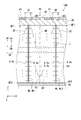
- (A) is a cross-sectional view showing a liquid crystal element (V1 ⁇ V2) according to the first modification of the first embodiment of the present invention.
- (B) is a figure which shows the retardation of the liquid crystal element (V1> V2) which concerns on the 1st modification. It is sectional drawing which shows the liquid crystal element which concerns on the 2nd modification of Embodiment 1 of this invention.
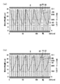
- (A) is a figure which shows the retardation of the liquid crystal element which comprises the wall part (directly below the unit electrode, V1 ⁇ V2) which concerns on Example 12A of this invention.
- (B) is a figure which shows the retardation of the liquid crystal element which comprises the wall part (directly under the unit electrode, V1> V2) which concerns on Example 12B of this invention. It is a figure which shows the retardation of the liquid crystal element which comprises the wall part (directly under the 1st electrode) which concerns on Example 13 of this invention. It is a figure which shows the retardation of the liquid crystal element which comprises the wall part (directly under the 2nd electrode) which concerns on Example 14 of this invention.
- the liquid crystal element 100 can function as, for example, a liquid crystal lens.
- the liquid crystal element 100 that functions as a liquid crystal lens can be used as a lens of an optical device.
- the optical device is, for example, eyeglasses, a head-mounted display, an endoscope, or a camera, but the application of the liquid crystal element 100 is not particularly limited.
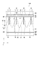
- FIG. 1A is a cross-sectional view showing the liquid crystal element 100.
- the liquid crystal element 100 includes a substrate SB1, a plurality of unit electrodes 10, an insulating layer LR, an alignment film AF1, a liquid crystal layer LQ, an alignment film AF2, and a counter electrode 20.
- a plurality of wall portions WL and a substrate SB2 are provided.
- the counter electrode 20 corresponds to an example of an “electrode”.
- a plurality of unit electrodes 10, an insulating layer LR, an alignment film AF1, a liquid crystal layer LQ, an alignment film AF2, a counter electrode 20, and a plurality of wall portions WL are arranged between the substrate SB1 and the substrate SB2.
- An insulating layer LR, an alignment film AF1, a liquid crystal layer LQ, an alignment film AF2, and a plurality of wall portions WL are arranged between the plurality of unit electrodes 10 and the counter electrode 20.
- the insulating layer LR and the alignment film AF1 are arranged between the plurality of unit electrodes 10 and the liquid crystal layer LQ.
- the alignment film AF1 is arranged at the interface BF1 of the liquid crystal layer LQ.
- the interface BF1 indicates a surface of the liquid crystal layer LQ on the side of the plurality of unit electrodes 10.
- An alignment film AF1, a liquid crystal layer LQ, an alignment film AF2, and a plurality of wall portions WL are arranged between the insulating layer LR and the counter electrode 20.
- the alignment film AF2 is arranged at the interface BF2 of the liquid crystal layer LQ.
- the interface BF2 indicates a surface of the liquid crystal layer LQ on the side of the counter electrode 20.
- the interface BF1 and the interface BF2 face the first direction D1.
- the first direction D1 indicates a direction substantially orthogonal to the unit electrode 10 and the counter electrode 20.
- the first direction D1 is substantially orthogonal to the interface BF1 and the interface BF2 of the liquid crystal layer LQ.
- the first direction D1 includes direction Da and direction Db.
- the direction Da indicates a direction from the side of the counter electrode 20 toward the side of the plurality of unit electrodes 10.
- the direction Db is a direction opposite to the direction Da, and indicates a direction from the side of the plurality of unit electrodes 10 toward the side of the counter electrode 20.
- the second direction D2 is substantially orthogonal to the first direction D1. In other words, the second direction D2 is substantially parallel to the interface BF1 and the interface BF2.
- the substrate SB1 has a substantially flat plate shape.
- the substrate SB1 is, for example, transparent and is made of glass or synthetic resin. As used herein, transparency includes colorless transparent, colored transparent, and translucent.
- Each of the plurality of unit electrodes 10 is arranged in the same layer.
- the plurality of unit electrodes 10 are arranged at intervals from each other.
- Each of the plurality of unit electrodes 10 includes a first electrode 1 and a second electrode 2.
- the first electrode 1 and the second electrode 2 constituting each unit electrode 10 are arranged at intervals from each other.
- Each of the first electrode 1 and the second electrode 2 is transparent, for example, and is formed of ITO (Indium Tin Oxide).
- Each of the first electrode 1 and the second electrode 2 has, for example, a metal mesh such as copper, a laminated structure of ITO and metal mesh, or a laminated structure or mixture of conductive carbon black fiber and ITO. It may be formed by the body, and the material is not particularly limited.
- a first voltage V1 is applied to the first electrode 1. Then, the first electrode 1 applies the first voltage V1 to the liquid crystal layer LQ.
- the first voltage V1 is an AC voltage.
- a second voltage V2 is applied to the second electrode 2. Then, the second electrode 2 applies a second voltage V2 to the liquid crystal layer LQ.
- the second voltage V2 is an AC voltage.
- the first voltage V1 and the second voltage V2 are different.
- the effective value of the first voltage V1 and the effective value of the second voltage V2 are different.
- the frequency of the first voltage V1 and the frequency of the second voltage V2 may be the same or different.
- the insulating layer LR is an electrical insulator.
- the insulating layer LR is, for example, transparent and is made of silicon dioxide (SiO 2 ).
- the insulating layer LR may be formed of, for example, a metal oxide other than silicon dioxide or an organic thin film, and the material is not particularly limited.
- the alignment film AF1 determines the orientation of the liquid crystal molecules in the liquid crystal layer LQ.
- the alignment film AF1 is, for example, a transparent and polyimide film.
- the liquid crystal layer LQ is composed of liquid crystal. Therefore, the liquid crystal layer LQ contains a large number of liquid crystal molecules.
- the liquid crystal constituting the liquid crystal layer LQ is, for example, a nematic liquid crystal and is transparent.
- the orientation of the liquid crystal is a homogeneous orientation in an environment without an electric field. Homogeneous orientation indicates a state in which the director of the liquid crystal molecule is substantially parallel to the second direction D2.
- the orientation of the liquid crystal may be homeotropic orientation in an environment without an electric field.
- the homeotropic orientation indicates a state in which the director of the liquid crystal molecule is substantially perpendicular to the second direction D2.
- the alignment film AF2 determines the orientation of the liquid crystal molecules in the liquid crystal layer LQ.
- the alignment film AF2 is, for example, a transparent and polyimide film.
- the counter electrode 20 faces the plurality of unit electrodes 10 via the insulating layer LR and the liquid crystal layer LQ.
- the counter electrode 20 is a substantially planar electrode.
- the counter electrode 20 is, for example, transparent and is formed of ITO.
- a third voltage V3 is applied to the counter electrode 20.
- the counter electrode 20 applies a third voltage V3 to the liquid crystal layer LQ.
- the counter electrode 20 is grounded, and the third voltage V3 is set to the ground potential (0V).
- the substrate SB2 has a substantially flat plate shape.
- the substrate SB2 is, for example, transparent and is made of glass.
- the plurality of wall portions WL are arranged on the liquid crystal layer LQ. Each of the plurality of wall portions WL extends along the second direction D2. The plurality of wall portions WL are substantially parallel to each other. Each of the plurality of wall portions WL faces the plurality of unit electrodes 10.
- the wall WL is, for example, transparent.
- the wall portion WL is composed of an electric insulator, a high resistor, or an electric conductor. In the present specification, the electrical resistivity of a high resistor is larger than the electrical resistivity of an electric conductor and smaller than the electrical resistivity of an electric insulator.
- the surface resistance of a high resistor is 5 ⁇ 10 3 ⁇ / ⁇ or more and 5 ⁇ 10 9 ⁇ / ⁇ or less
- the surface resistance of an electric conductor is 5 ⁇ 10 -1 ⁇ / ⁇ or more and 5 ⁇ 10 2 ⁇ / It is ⁇ or less
- the surface resistance of the electrical insulator is 1 ⁇ 10 11 ⁇ / ⁇ or more and 1 ⁇ 10 15 ⁇ / ⁇ or less.
- the surface resistance of a high resistor is 1 ⁇ 10 2 ⁇ / ⁇ or more and 1 ⁇ 10 11 ⁇ / ⁇ or less
- the surface resistance of an electric conductor is 1 ⁇ 10 -2 ⁇ / ⁇ or more and 1 ⁇ 10 2 ⁇ / ⁇ or less
- the surface resistance of the electrical insulator may be 1 ⁇ 10 11 ⁇ / ⁇ or more and 1 ⁇ 10 16 ⁇ / ⁇ or less. It should be noted that these examples do not limit the surface resistance of the high resistor, the surface resistance of the electric conductor, and the surface resistance of the electric conductor in the application of the present invention.
- the liquid crystal layer LQ has a wavy retardation RT.
- Has. "Wavy” indicates a continuous shape in which large and small extrema are repeated alternately.
- the retardation is an amount indicating the phase difference between the two waves caused by the phenomenon that the light incident on the liquid crystal layer LQ is divided into two light waves (for example, normal light and abnormal light) having vibration directions perpendicular to each other.
- R is retardation
- ⁇ n is birefringence of the liquid crystal layer LQ
- d is the thickness of the liquid crystal layer LQ.
- ⁇ n can change depending on the tilt angle of the liquid crystal molecule with respect to the second direction D2. Therefore, the retardation can also change depending on the tilt angle of the liquid crystal molecule with respect to the second direction D2.
- ⁇ n ne ( ⁇ ) -no. no indicates the refractive index for normal light. no does not depend on the angle of the incident light with respect to the optical axis OP. In other words, no does not depend on the inclination angle ⁇ of the optical axis OP with respect to the second direction D2.
- the optical axis OP indicates the optical axis of the liquid crystal molecule, and is a direction in which light is not separated even if light is incident on the liquid crystal having optical anisotropy.
- ne ( ⁇ ) indicates the refractive index for abnormal light. ne ( ⁇ ) changes depending on the angle of the incident light with respect to the optical axis OP.
- ne ( ⁇ ) changes depending on the inclination angle ⁇ of the optical axis OP with respect to the second direction D2. Therefore, the retardation also changes depending on the inclination angle ⁇ of the optical axis OP of the liquid crystal molecule with respect to the second direction D2.
- a plurality of liquid crystal molecules located along the first direction D1 (Z direction) on a certain X coordinate X1.
- the tilt angle ⁇ of the optical axis OP of (may be described) is a plurality of liquid crystal molecules (hereinafter, “plurality of liquid crystals”) located along the first direction D1 (Z direction) on the other X coordinate X2. It may be described as "molecule ML2"), which is different from the tilt angle ⁇ of the optical axis OP, and the retardation at the X coordinate X1 and the retardation at the X coordinate X2 are different.
- the inclination angles ⁇ of the optical axes OP of the plurality of liquid crystal molecules ML1 on the X coordinate X1 are the same, and the plurality of liquid crystal molecules on the X coordinate X2 are made the same.
- the tilt angle ⁇ of the optical axis OP of the ML2 was made the same.
- the retardation at a certain X coordinate X1 can be calculated as follows. That is, in the liquid crystal layer LQ, a plurality of liquid crystal molecules ML1 exist along the first direction D1 (Z direction) on a certain X coordinate X1. In reality, the inclination angles ⁇ of the optical axes OP of the plurality of liquid crystal molecules ML1 are not the same in the liquid crystal driving state. Therefore, the retardation at the X coordinate X1 is calculated by integrating ⁇ n for each of the plurality of liquid crystal molecules ML1 from the thickness 0 to the thickness d.
- the retardation of the liquid crystal portion in which the director of the liquid crystal molecule is substantially orthogonal to the interface BF1 or the interface BF2 is minimized.
- the retardation of the liquid crystal portion in which the director of the liquid crystal molecules is substantially parallel to the interface BF1 or the interface BF2 is maximized.
- a plurality of unit electrodes 10 are arranged, the first voltage V1 is applied to the first electrode 1, and the second voltage V2 is applied to the second electrode 2, so that the liquid crystal layer LQ is subjected to. Wavy retardation RT occurs.
- the plurality of peaks P1 of the wavy retardation RT correspond to the positions of the plurality of wall portions WL, respectively. Therefore, according to the first embodiment, by arranging the plurality of wall portions WL on the liquid crystal layer LQ, even in the portion of the liquid crystal layer LQ corresponding to the unit electrode 10 having a relatively small width dw, the wavy attenuation RT can be formed. It is possible to suppress the attenuation of the amplitude difference (P1-P2). As a result, a relatively large refraction angle of light can be realized even in the liquid crystal portion corresponding to the unit electrode 10 having a relatively small width dw in the liquid crystal layer LQ.
- the plurality of peaks P1 of the wavy retardation RT are located at the positions of the plurality of wall portions WL, respectively. That is, the position of the peak P1 in the second direction D2 (X direction) is substantially the same as the position of the wall portion WL in the second direction D2 (X direction). However, the peak P1 may be located at a position close to the wall portion WL in the second direction D2.
- the "position close to the wall portion WL" is a position within ⁇ 15% of the interval DT with respect to the wall portion WL in the second direction D2, and the interval with respect to the wall portion WL in the second direction D2.
- the position is preferably within the range of ⁇ 10% of the DT, and more preferably the position is within the range of ⁇ 5% of the interval DT with respect to the wall portion WL in the second direction D2.
- the interval DT indicates the interval in the second direction D2 between the wall portion WL and the wall portion WL adjacent to each other.
- the position of the peak P1 in the first direction D1 (Z direction) is not particularly limited.
- the "amplitude difference" indicates the difference between the peak P1 and the extremum P2 adjacent to the peak P1 in the wavy retardation RT.
- Peak P1 indicates the local maximum value of wavy retardation RT. Therefore, the magnitudes of the plurality of peaks P1 may be different or the same.
- the extremum P2 indicates the local minimum value of wavy retardation RT. Therefore, the magnitudes of the plurality of extremums P2 may be different or the same.
- the retardation RT can be measured as follows.
- the liquid crystal element 100 is arranged between the orthogonal polarizers. Then, when the transmittance is obtained by measuring the transmission spectrum between the orthogonal polarizers, ⁇ n can be obtained from the transmittance.
- the thickness d of the liquid crystal layer LQ is measured by a thickness measuring device. Then, the retardation is calculated by ⁇ n ⁇ d. Further, for example, when the cross Nicol observation of the liquid crystal element 100 is performed with a polarizing microscope, the interference fringes represent the retardation RT.
- FIG. 2 is a cross-sectional view schematically showing the state of the liquid crystal molecules 5 contained in the liquid crystal layer LQ.
- the first voltage V1 applied to the first electrode 1 is smaller than the second voltage V2 applied to the second electrode 2.
- the substrates SB1 and SB2 are omitted for simplification of the drawings.
- the liquid crystal layer LQ contains a large number of liquid crystal molecules 5.
- the director of the liquid crystal molecules 5y is substantially orthogonal to the interfaces BF1 and BF2 by the second voltage V2, for example. Therefore, the extreme value P2 of the retardation RT occurs in the region AR.
- the director of the liquid crystal molecules 5x in contact with the wall portion WL faces, for example, a direction substantially parallel to the interface BF1 and the interface BF2 of the liquid crystal layer LQ. That is, among the liquid crystal molecules 5 constituting the liquid crystal layer LQ, the director of the liquid crystal molecules 5x in contact with the wall portion WL faces the direction along the interface BF1 and the interface BF2 of the liquid crystal layer LQ. Therefore, according to the first embodiment, the peak P1 of the retardation RT becomes large at the position of the wall portion WL. As a result, the attenuation of the amplitude difference of the wavy retardation RT can be suppressed.
- the director of the liquid crystal molecules 5x is directed along the interface BF1 and the interface BF2 even by the interaction between the wall portion WL, the liquid crystal molecules 5x, and the electric field. It is presumed to face.
- the director of the liquid crystal molecule 5x in contact with the wall portion WL is relative to the interface BF1 and the interface BF2. It may be oriented in the direction of inclination.
- the liquid crystal molecules 5 are separated from the wall portion WL1 due to the continuity of the liquid crystal molecules 5. It gradually changes from a lying state to an upright state toward the region AR. Further, also in the region between the region AR and the other wall portion WL2, the orientation of the liquid crystal molecules 5 changes from the standing state to the lying state from the region AR toward the wall portion WL2 due to the continuity of the liquid crystal molecules 5. It changes gradually. As a result, as shown in FIG. 2, a wavy retardation RT having a plurality of peaks P1 and a plurality of extremums P2 is generated.
- the wall portion WL extends from the side of the counter electrode 20 to the side of the unit electrode 10 in the liquid crystal layer LQ. Therefore, in the liquid crystal layer LQ, the director of the liquid crystal molecules 5x in contact with the wall portion WL faces the direction along the interface BF1 and the interface BF2 from the side of the counter electrode 20 to the side of the unit electrode 10. As a result, the peak P1 of the wavy retardation RT becomes large, and the attenuation of the amplitude difference of the retardation RT can be effectively suppressed.
- the wall portion WL extends from the interface BF2 of the liquid crystal layer LQ to the interface BF1.
- the director of the liquid crystal molecule 5 can be measured as follows. For example, directly observe the orientation or order parameters of the liquid crystal by polarized Raman spectroscopy or polarized infrared spectroscopy. For example, as an indirect optical method, the direction of refractive index anisotropy or the dielectric anisotropy is observed.
- the thickness t of the wall portion WL indicates the thickness of the wall portion WL in the second direction D2.
- the thickness t of the wall portion WL is preferably smaller than, for example, the width of the first electrode 1 or the width of the second electrode 2.
- the thickness t of the wall portion WL is preferably smaller than, for example, the width of the region 90 or the width of the region 92.
- the thickness t of the wall portion WL is, for example, preferably 5 ⁇ m or less, and more preferably 1 ⁇ m or less.
- the region 90 indicates a region of the insulating layer LR between the first electrode 1 and the second electrode 2 constituting the unit electrode 10.
- the area 90 may be a space.
- the region 92 indicates a region of the insulating layer LR between the unit electrodes 10 adjacent to each other.
- the area 92 may be a space.
- the wavy retardation RT has a plurality of convex portion PRs.
- Each of the convex portions PR is asymmetric with respect to the peak P1.
- Each of the convex portions PR shows, for example, an asymmetrical mountain shape.
- the wall portion WL faces the region 90 of the insulating layer LR and the first direction D1 via the alignment film AF1. Therefore, when the first voltage V1 applied to the first electrode 1 is smaller than the second voltage V2 applied to the second electrode 2, each of the plurality of convex portions PR has a gently sloping portion C1 with the peak P1 in between. And the steeply inclined portion C2.
- the gently inclined portion C1 corresponds to the first electrode 1.
- the steeply inclined portion C2 corresponds to the second electrode 2.
- the inclination of the gently inclined portion C1 is gentler than the inclination of the steeply inclined portion C2.
- the retardation RT has, for example, a shape that repeats a substantially inverted N shape. The case where the first voltage V1 is larger than the second voltage V2 will be described later.
- the focal length of the convex lens when switching the magnitude relationship between the first voltage V1 and the second voltage V2 and switching the liquid crystal element 100 functioning as a liquid crystal lens between the convex lens and the concave lens, the focal length of the convex lens
- the magnitude of (for example, a positive value) and the magnitude of the focal length (for example, a negative value) of a concave lens can be substantially matched. As a result, it is highly convenient for the user or designer of the liquid crystal element 100.
- the width of the region 92 of the insulating layer LR is substantially the same as the width of the region 90.
- the width of the region 92 and the width of the region 90 are not particularly limited.
- the width of the region 92 is smaller than the width of the region 90, by arranging the wall portion WL facing the region 90, the wall portion WL is arranged so as to face the region 92 as compared with the case where the wall portion WL is arranged facing the region 92. The formation of WL becomes easy.
- region AR1 in the liquid crystal layer LQ, in a certain region (hereinafter, referred to as “region AR1”) between the wall portions WL adjacent to each other, the director of the liquid crystal molecule 5y is subjected to the first voltage V1. For example, it faces a direction substantially orthogonal to the interface BF1 and the interface BF2. Therefore, in the liquid crystal layer LQ, the extreme value P2 of the retardation RT is generated in the region AR1 between the wall portions WL adjacent to each other.
- FIG. 1B is a diagram showing a retardation RT when the first voltage V1 applied to the first electrode 1 is larger than the second voltage V2 applied to the second electrode 2.
- each of the plurality of convex portion PRs constituting the wavy retardation RT is a steeply inclined portion with the peak P1 in between.
- the steeply inclined portion C3 corresponds to the first electrode 1.
- the gently inclined portion C4 corresponds to the second electrode 2.
- the inclination of the gently inclined portion C4 is gentler than the inclination of the steeply inclined portion C3.
- the retardation RT has, for example, a shape that repeats a substantially N-shape.
- the light incident substantially perpendicular to the liquid crystal layer LQ is refracted toward the gently inclined portion C4.
- light incident substantially perpendicular to the liquid crystal layer LQ is refracted diagonally upward to the right.
- the anchoring energy of the wall portion WL is preferably 1 ⁇ 10 -6 (J / m 2 ) or more.
- the wall WL can secure sufficient anchoring energy to direct the director of the liquid crystal molecules 5x in contact with the wall WL in the direction along the interfaces BF1 and BF2.
- the anchoring energy can be measured as follows.
- anchoring energy can be measured by the saturation threshold voltage method derived from a generalized surface anchoring model.
- the wall surface of the wall portion WL is composed of a polymer. Therefore, since the anchoring energy of the wall portion WL is increased by the polymer chain, the liquid crystal molecules 5x in contact with the wall portion WL are effectively oriented along the interfaces BF1 and BF2 of the liquid crystal layer LQ. As a result, the attenuation of the amplitude difference of the wavy retardation RT can be effectively suppressed.
- the polymer is, for example, an electrical insulator or a high resistor.
- the polymer is, for example, polyimide.
- the polymer may be, for example, an electric conductor (for example, a conductive polymer).
- the conductive polymer is, for example, PEDOT: PSS (poly (4-styrene sulfonic acid) doped poly (3,4-ethylenedioxythiophene)) or polypyrrole.
- the entire wall portion WL may be composed of a polymer, or only the wall surface of the wall portion WL may be composed of a polymer.
- the wall portion WL may be composed of a wall portion main body and a polymer film formed on the surface of the wall portion main body.
- the material of the wall body is not particularly limited.
- the wall body may be an electrical insulator, a high resistor, or an electrical conductor.
- the wall surface of the wall portion WL is composed of a substance having a polar portion. Therefore, since the anchoring energy of the wall portion WL increases depending on the polar portion, the liquid crystal molecules 5x in contact with the wall portion WL are effectively oriented along the interfaces BF1 and BF2 of the liquid crystal layer LQ. As a result, the attenuation of the amplitude difference of the wavy retardation RT can be effectively suppressed.
- a substance having a polar moiety is, for example, an electrical insulator or a high resistor.
- the substance having a polar moiety is, for example, polyimide.
- the entire wall portion WL may be composed of a substance having a polar portion, or only the wall surface of the wall portion WL may be composed of a substance having a polar portion.
- the wall portion WL may be composed of a wall portion main body and a film of a substance having a polar portion formed on the surface of the wall portion main body.
- the material of the wall body is not particularly limited.
- the wall body may be an electrical insulator, a high resistor, or an electrical conductor.
- the wall surface of the wall portion WL is composed of a polymer having a polar portion. Therefore, since the anchoring energy of the wall portion WL is increased by the polar portion and the polymer chain, the liquid crystal molecules 5x in contact with the wall portion WL are effectively oriented along the interfaces BF1 and BF2 of the liquid crystal layer LQ. As a result, the attenuation of the amplitude difference of the wavy retardation RT can be effectively suppressed.
- the polymer having a polar moiety is, for example, an electrical insulator or a high resistor.
- the polymer having a polar moiety is, for example, polyimide.
- the entire wall portion WL may be composed of a polymer having a polar portion, or only the wall surface of the wall portion WL may be composed of a polymer having a polar portion.
- the wall portion WL may be composed of a wall portion main body and a polymer film having a polar portion formed on the surface of the wall portion main body.
- the material of the wall body is not particularly limited.
- the wall body may be an electrical insulator, a high resistor, or an electrical conductor.
- a liquid crystal for example, a biphenyl liquid crystal
- a solution of a photocurable liquid crystal monomer are irradiated with light, and this monomer is polymerized to form a wall portion WL as a high-density polymer network structure.
- the liquid crystal / liquid crystal monomer solution is sandwiched between the substrates with the polyimide alignment film, the liquid crystal monomer having an elongated molecular structure is spontaneously oriented together with the liquid crystal. Then, the polymer is selectively precipitated and hardened on the irradiated portion by the pattern exposure of ultraviolet rays.
- the monomer in the non-irradiated region of ultraviolet rays is thermally diffused or concentrated and captured in the irradiated portion, so that the polymer aggregate grows on the substrate surface and the polymer wall as the wall portion WL.
- the wall portion WL is composed of a polymer formed from a photocurable liquid crystal monomer.
- photocurable liquid crystal monomers are lined up. Therefore, the liquid crystal molecules 5 in contact with the wall portion WL are oriented along the arrangement of the photocurable liquid crystal monomers. In other words, the orientation of the liquid crystal molecules 5 in contact with the wall portion WL can be determined by the initial orientation state of the photocurable liquid crystal monomer.
- the wall portion WL may be manufactured by using nanoimprint lithography (for example, optical imprint or thermal imprint) or photolithography.
- the wall portion WL when the wall portion WL is composed of an electric insulator, the wall portion WL may be formed of a photopolymerizable resin.
- conductive particles are added or filled in the semi-conductive resin, or carbon black fibers are dispersed in the semi-conductive resin to disperse the wall portion WL. To create.
- a specific process may be executed on the surface of the wall portion WL.
- the specific treatment is, for example, a hydrophobizing treatment, a hydrophilization treatment, or a plasma treatment.
- the pre-twist angle of the liquid crystal molecule 5 indicates the angle formed by the long axis of the liquid crystal molecules 5 with respect to the reference line BL when the liquid crystal molecules 5 are viewed in a plan view.
- plane view indicates that the object is viewed from the first direction D1.
- the pre-twist angle is determined by the alignment films AF1 and AF2.
- FIGS. 3A to 3D are views showing the state of the liquid crystal molecules 5 in contact with the wall portion WL.
- the wall portion WL and the liquid crystal molecule 5 are viewed from the direction Dz of FIG.
- the pre-twist angle formed by the long axis of the liquid crystal molecule 5 with respect to the reference line BL is 45 degrees.
- the reference line BL is substantially orthogonal to the wall portion WL.
- the pre-twist angle formed by the long axis of the liquid crystal molecule 5 with respect to the reference line BL is 0 degrees.
- the pre-twist angle formed by the long axis of the liquid crystal molecule 5 with respect to the reference line BL is 90 degrees.
- the pre-twist angle formed by the long axis of the liquid crystal molecules 5 with respect to the reference line BL in the alignment film AF2 is 0 degrees.
- the pre-twist angle formed by the major axis of the liquid crystal molecule 5 with respect to the reference line BL in the alignment film AF1 is 90 degrees. Therefore, the plurality of liquid crystal molecules 5 are arranged so as to be twisted between the alignment film AF1 and the alignment film AF2.
- the present invention can be applied without depending on the pre-twist angle of the liquid crystal molecule 5. This is because the retardation RT increases as the director of the liquid crystal molecule 5 approaches the direction along the interfaces BF1 and BF2 of the liquid crystal layer LQ (the direction parallel to the interfaces BF1 and BF2), while the pre-twist angle of the liquid crystal molecule 5 increases. Is independent. For example, as long as the director of the liquid crystal molecules 5x in contact with the wall portion WL points in the direction along the interfaces BF1 and BF2 of the liquid crystal layer LQ, it is wavy without depending on the pre-twist angle of the liquid crystal molecules 5. It is possible to suppress the attenuation of the amplitude difference of the retardation RT.
- the first modification to the fifth modification of the first embodiment will be described with reference to FIGS. 4A to 8.
- the arrangement of the wall portion WL is mainly different from that of the first embodiment described with reference to FIGS. 1 and 2.
- the length of the wall portion WL is mainly different from that of the first embodiment described with reference to FIGS. 1 and 2.
- the points that the first modification to the fifth modification are different from the first embodiment will be mainly described.
- FIG. 4A is a cross-sectional view showing the liquid crystal element 100B according to the first modification.
- the wall portion WL is formed in the region 92 between the unit electrodes 10 and the unit electrodes 10 adjacent to each other and the first direction D1 via the alignment film AF1. opposite. Therefore, when the first voltage V1 applied to the first electrode 1 is smaller than the second voltage V2 applied to the second electrode 2, each of the plurality of convex portion PRs constituting the wavy retardation RT has a peak P1. A steeply inclined portion C3 and a gently inclined portion C4 are included. That is, the convex portion PR has a shape in which the convex portion PR shown in FIG. 1A of the first embodiment is horizontally inverted.
- the retardation RT has, for example, a shape that repeats a substantially N-shape.
- FIG. 4B is a diagram showing a retardation RT when the first voltage V1 applied to the first electrode 1 is larger than the second voltage V2 applied to the second electrode 2.
- each of the plurality of convex portion PRs constituting the wavy retardation RT has a gently sloping portion with the peak P1 in between. Includes C1 and steeply inclined portion C2. That is, the convex portion PR has a shape in which the convex portion PR shown in FIG. 1 (b) of the first embodiment is horizontally inverted.
- the retardation RT has, for example, a shape that repeats a substantially inverted N shape.
- FIG. 5 is a cross-sectional view showing the liquid crystal element 100B according to the second modification.
- the wall portion WL faces the first electrode 1 and the first direction D1 via the alignment film AF1.
- the first voltage V1 applied to the first electrode 1 is smaller than the second voltage V2 applied to the second electrode 2. Therefore, each of the plurality of convex portion PRs constituting the wavy retardation RT includes a steeply inclined portion C3 and a gently inclined portion C4 with the peak P1 in between.
- the retardation RT has, for example, a shape that repeats a substantially N-shape.
- FIG. 6 is a cross-sectional view showing the liquid crystal element 100D according to the third modification.
- the wall portion WL faces the second electrode 2 and the first direction D1 via the alignment film AF1.
- the first voltage V1 applied to the first electrode 1 is smaller than the second voltage V2 applied to the second electrode 2. Therefore, each of the plurality of convex portion PRs constituting the wavy retardation RT includes a gently sloping portion C1 and a steeply sloping portion C2 with the peak P1 in between.
- the retardation RT has, for example, a shape that repeats a substantially inverted N shape.
- FIG. 7 is a cross-sectional view showing the liquid crystal element 100E according to the fourth modification.
- the length L of the wall portion WL is shorter than the thickness d of the liquid crystal layer LQ.
- the length L indicates the length of the wall portion WL in the first direction D1.
- the wall portion WL extends in the direction Da from the side of the counter electrode 20 toward the side of the plurality of unit electrodes 10.
- the wall portion WL faces the unit electrode 10. Specifically, the wall portion WL faces the region 90.
- FIG. 8 is a cross-sectional view showing the liquid crystal element 100F according to the fifth modification.
- the length L of the wall portion WL is shorter than the thickness d of the liquid crystal layer LQ.
- the length L indicates the length of the wall portion WL in the first direction D1.
- the wall portion WL extends in the direction Db from the side of the plurality of unit electrodes 10 toward the side of the counter electrode 20.
- the wall portion WL faces the unit electrode 10. Specifically, the wall portion WL faces the region 90.
- the fifth modification by shortening the length L of the wall portion WL, it is possible to suppress that the light passing through the liquid crystal layer LQ is directly affected by the wall portion WL.
- the wall portion WL may face the region 92, the first electrode 1, or the second electrode 2.
- the liquid crystal elements 100, 100A to 100F may be provided with a high resistance layer (resistance layer) composed of a high resistor instead of the insulating layer LR. Good. Further, as long as the liquid crystal elements 100, 100A to 100F include the unit electrode 10, the liquid crystal layer LQ, and the wall portion WL, the present invention can be applied, and the liquid crystal elements 100, 100A to 100F can be applied.
- the structure is not particularly limited. Similarly, the present invention can be applied without particularly limiting the specific structures of the unit electrode 10, the liquid crystal layer LQ, and the wall portion WL.
- the liquid crystal element 100G according to the second embodiment of the present invention will be described with reference to FIG.
- the second embodiment is mainly different from the first embodiment in that the liquid crystal element 100G includes the high resistance layer 30.
- the points that the second embodiment differs from the first embodiment will be mainly described.
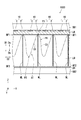
- FIG. 9 is a cross-sectional view showing the liquid crystal element 100G according to the second embodiment.
- the liquid crystal element 100G includes a plurality of high resistance layers 30 (plurality of resistance layers) in addition to the configuration of the liquid crystal element 100 according to the first embodiment described with reference to FIG. 1A.
- the high resistance layer 30 is composed of a high resistance body (resistor). Therefore, the resistivity of the high resistivity layer 30 is larger than the resistivity of the electric conductor and smaller than the resistivity of the electric insulator.
- a plurality of high resistance layers 30 are arranged in the same layer.
- the plurality of high resistance layers 30 are arranged between the plurality of unit electrodes 10 and the liquid crystal layer LQ.
- the insulating layer LR is sandwiched between the plurality of unit electrodes 10 and the plurality of high resistance layers 30.
- the plurality of high resistance layers 30 face each of the plurality of unit electrodes 10 and the first direction D1 via the insulating layer LR.
- the wall portion WL faces the high resistance layer 30 and the first direction D1 via the alignment film AF1.
- the wall portion WL faces the region 90 and the first direction D1 via the alignment film AF1 and the high resistance layer 30.
- the high resistance layer 30 is transparent and is formed of zinc oxide (ZnO).
- the material of the high resistance layer 30 is not particularly limited as long as the high resistance layer 30 is composed of the high resistance body.
- the high resistance layer 30 may be a mixture of zinc oxide and another substance, or may be an organic thin film.
- the high resistance layer 30 is provided, so that the liquid crystal layer LQ has a smooth potential.
- a gradient is formed.
- the light incident on the liquid crystal element 100G can be accurately refracted at a refraction angle corresponding to the potential gradient.
- a substantially serrated potential gradient is formed in the liquid crystal layer LQ corresponding to the plurality of unit electrodes 10.
- the substantially serrated potential gradient is composed of a plurality of linear or curved potential gradients, and each potential gradient has a smooth linear shape or curved shape.
- the second embodiment includes a plurality of wall portions WL as in the first embodiment. Therefore, in the second embodiment, as in the first embodiment, the amplitude difference (P1-P2) of the wavy retardation RT is attenuated even in the portion of the liquid crystal layer LQ corresponding to the unit electrode 10 having a relatively small width dw. Can be suppressed.
- the liquid crystal element 100G according to the second embodiment has the same effect as the liquid crystal element 100 according to the first embodiment.
- the characteristics of the shape of the retardation RT of the liquid crystal element 100G are the same as the characteristics of the shape of the retardation RT of the liquid crystal element 100 according to the first embodiment (FIGS. 1 (a) and 1 (b)). Note that FIG. 9 shows an example in which the first voltage V1 is smaller than the second voltage V2.
- the liquid crystal elements 100B to 100F may include a plurality of high resistance layers 30.
- the wall portion WL faces the first electrode 1 or the second electrode 2 and the first direction D1 via the high resistance layer 30.
- the characteristics of the shape of the retardation RT are the same as the characteristics of the shape of the retardation RT when the high resistance layer 30 does not exist. ..
- the structure of the liquid crystal element 100G is an example, and the present invention can be applied as long as the liquid crystal element 100G includes a unit electrode 10, a liquid crystal layer LQ, and a wall portion WL.
- the structure of the liquid crystal element 100G is not particularly limited.
- the present invention can be applied without particularly limiting the specific structures of the unit electrode 10, the liquid crystal layer LQ, and the wall portion WL.
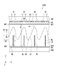
- the liquid crystal element 100H according to the third embodiment of the present invention will be described with reference to FIGS. 10 and 11.
- the third embodiment is mainly different from the second embodiment in that the liquid crystal element 100H constitutes a liquid crystal lens (specifically, a Fresnel lens).
- a liquid crystal lens specifically, a Fresnel lens
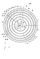
- FIG. 10 is a schematic plan view showing the liquid crystal element 100H according to the third embodiment.
- the liquid crystal element 100H has an optical axis AX.
- the optical axis AX corresponds to the optical axis of the liquid crystal element 100H that functions as a liquid crystal lens.
- the optical axis AX is a virtual straight line passing through the center and the focal point of the liquid crystal element 100H that functions as a liquid crystal lens. That is, the optical axis AX is a virtual straight line that coincides with the rotational symmetry axis of the liquid crystal element 100H that functions as a liquid crystal lens and is orthogonal to the liquid crystal element 100H.
- the liquid crystal element 100H includes a liquid crystal layer LQ, a core electrode CR, a center electrode CT, a plurality of unit electrodes rn, a plurality of wall portions WL, a first lead wire 71, and a second lead wire 72.
- Each of the plurality of unit electrodes rn includes a first electrode 1 and a second electrode 2.
- the center electrode CT, the first electrode 1, the second electrode 2, the plurality of wall portions WL, the first lead wire 71, and the second lead wire 72 are shown in a simplified manner.
- n of the reference code “rn” assigned to the unit electrode rn is assigned to each of the plurality of unit electrodes in ascending order from the unit electrode having the smallest radius to the unit electrode having the largest radius among the plurality of unit electrodes. It is an integer of 1 or more and N or less. In the example of FIG. 10, since the liquid crystal element 100H includes five unit electrodes rn, N is “5”.
- the unit electrode rn has a radius Rn.
- the subscript n of the reference code "Rn” corresponds to the subscript n of the reference code "rn”.
- the radius Rn of the unit electrode rn is larger than the unit electrode rn outside the radial direction RD (R5> R4> R3> R2> R1).
- the radius Rn of the unit electrode rn indicates the distance from the optical axis AX to the second electrode 2 constituting the unit electrode rn.
- the core electrode CR, the center electrode CT, and the plurality of unit electrodes rn are arranged substantially concentrically with respect to the optical axis AX.
- the width dn of the plurality of unit electrodes rn is as small as the unit electrode rn located outside the radial RD with respect to the optical axis AX.
- the subscript n of the reference code "dn" corresponds to the subscript n of the reference code "rn”.
- the width dn indicates the width of the radial RD of the unit electrode rn.
- the core electrode CR has a disk-like shape and is arranged on the optical axis AX of the liquid crystal element 100H.
- the core electrode CR is formed of the same material as the first electrode 1.
- the core electrode CR applies a first voltage V1 to the liquid crystal layer LQ.
- the center electrode CT surrounds the core electrode CR.
- the plurality of unit electrodes rn are arranged outside the radial RD with respect to the center electrode CT.
- the center electrode CT applies a second voltage V2 to the liquid crystal layer LQ.
- the center electrode CT is formed of the same material as the second electrode 2.
- each of the center electrode CT, the first electrode 1, and the second electrode 2 has a substantially annular shape.
- each of the center electrode CT, the first electrode 1, and the second electrode 2 has a substantially annular shape that is partially interrupted.
- each of the first electrodes 1 may be configured to form a substantially circular ring by a plurality of arcuate electrodes.
- each of the second electrodes 2 may be configured to form a substantially circular ring by a plurality of arcuate electrodes.
- the first lead wire 71 is connected to the core electrode CR and a plurality of first electrodes 1. Then, the first lead wire 71 applies a first voltage V1 to the core electrode CR and the plurality of first electrodes 1.
- the second lead wire 72 is connected to the center electrode CT and the plurality of second electrodes 2. Then, the second lead wire 72 applies a second voltage V2 to the center electrode CT and the plurality of second electrodes 2.
- the plurality of wall portions WL are arranged substantially concentrically with respect to the optical axis AX.
- Each of the plurality of wall portions WL has a substantially annular shape in a plan view.
- each of the plurality of wall portions WL may be configured to form a substantially circular ring by the plurality of arcuate wall portions in a plan view.
- the wavy attenuation is also performed in the portion of the liquid crystal layer LQ corresponding to the relatively small unit electrode rn having a width dn. It is possible to suppress the attenuation of the RT amplitude difference.
- the liquid crystal element 100H according to the third embodiment has the same effect as the liquid crystal elements 100 and 100G according to the first and second embodiments.
- the plurality of wall portions WL are arranged corresponding to the unit electrode rn located outside the radial direction RD from the predetermined position PS (dashed line) among the plurality of unit electrodes rn. That is, the wall portion WL is arranged corresponding to the unit electrode rn located outside the radial RD in which the decrease in the amplitude difference of the retardation RT is relatively large. Therefore, it is not necessary to arrange the wall portion WL with respect to the unit electrode rn located inside the radial RD in which the decrease in the amplitude difference of the retardation RT is relatively small. As a result, in the region inside the liquid crystal layer LQ, it is possible to suppress that the light passing through the liquid crystal layer LQ is directly affected by the wall portion WL. In other words, the number of wall WLs can be optimized.
- the attenuation of the amplitude difference of the retardation RT in the radial RD is set to the wall portion. Suppressed by WL.
- the liquid crystal portion driven by the unit electrode rn located inside the radial RD from the predetermined position PS has a relatively large width dn of the unit electrode rn, so that the retardation in the radial RD The attenuation of the RT amplitude difference does not occur or is very small.
- a sufficient amplitude difference of the retardation RT can be secured for each unit electrode rn over the entire liquid crystal layer LQ.
- the wave surface aberration of the liquid crystal element 100H that functions as a liquid crystal lens can be effectively reduced.
- the amplitude difference of the retardation RT is substantially constant in the plurality of liquid crystal portions corresponding to the plurality of unit electrodes rn from the inside to the outside of the radial RD in the liquid crystal layer LQ.
- a plurality of wall portions WL are arranged in the wall.
- the predetermined position PS indicates a position outside the innermost unit electrode rn in the radial direction among the plurality of unit electrodes rn.
- the predetermined position PS is the radial RD rather than the position in the liquid crystal layer LQ where the amplitude difference of the retardation RT of the liquid crystal portion driven by each unit electrode rn is substantially constant over the two or more unit electrodes rn. Indicates the position outside of.
- the distance between the first electrode 1 and the second electrode 2 sandwiching the alternate long and short dash line indicating the predetermined position PS is shown slightly larger than the others.
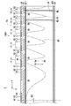
- FIG. 11 is a cross-sectional view showing the liquid crystal element 100H.
- the liquid crystal element 100H further includes an insulating layer LR, a high resistance layer 30, an alignment film AF1, an alignment film AF2, and a counter electrode 20.
- the counter electrode 20 corresponds to an example of an “electrode”.
- the plurality of high resistance layers 30 are arranged substantially concentrically with respect to the optical axis AX.
- the liquid crystal element 100H includes a substrate similar to the substrate SB1 shown in FIG. 1A and a substrate similar to the substrate SB2, but is omitted for simplification of the drawings.
- the effective value of the first voltage V1 is smaller than the effective value of the second voltage V2.
- FIG. 11 shows an example in which the first voltage V1 is smaller than the second voltage V2.
- Two or more peaks P1 of the plurality of peaks P1 of the wavy retardation RT correspond to the positions of the plurality of wall portions WL, respectively. Specifically, two or more peaks P1 of the plurality of peaks P1 of the wavy retardation RT are respectively located at the positions of the plurality of wall portions WL.
- the unit electrode rn located outside the radial direction RD from the predetermined position PS is the unit electrode r4 and the unit electrode r5. Therefore, two peaks P1 of the plurality of peaks P1 of the wavy retardation RT correspond to the position of the wall portion WL corresponding to the unit electrode r4 and the position of the wall portion WL corresponding to the unit electrode r5, respectively. ing.
- the wavy retardation RT has a plurality of extrema P2.
- the extremum P2 indicates the local minimum value of wavy retardation RT.
- the plurality of wall portions WL are arranged outside the radial direction RD from the predetermined position PS.
- the wall portion WL is arranged outside the predetermined position PS in the radial direction RD so as to face the unit electrode rn.
- the wall portion WL faces the region 90 of the insulating layer LR and the first direction D1.
- the director of the liquid crystal molecules in contact with the wall portion WL is along the radial direction RD. That is, in the liquid crystal driving state, the director of the liquid crystal molecules in contact with the wall portion WL is substantially parallel to the radial RD. Therefore, the peak P1 of the retardation RT can be increased in the wall portion WL.
- the first voltage V1 is applied to the core electrode CR
- the second voltage V2 is applied to the center electrode CT
- the first voltage V2 is applied to the unit electrode rn.
- a voltage V1 and a second voltage V2 are applied. Therefore, a serrated potential gradient symmetrical with respect to the optical axis AX can be formed on the liquid crystal layer LQ.
- the liquid crystal element 100H can function as a Fresnel lens.
- the liquid crystal element 100H can form a convex Fresnel lens.
- the maximum amplitude or effective value of the second voltage V2 is made larger than the maximum amplitude or effective value of the first voltage V1
- the liquid crystal element 100H can form a concave Fresnel lens.
- the wall portion WL may face the region 92, the first electrode 1, or the second electrode 2 and the first direction D1. Further, the length of the wall portion WL may be shorter than the thickness d of the liquid crystal layer LQ, as in the fourth modification or the fifth modification. Further, the core electrode CR may not be provided.
- the structure of the liquid crystal element 100H is an example, and the present invention can be applied as long as the liquid crystal element 100H includes a unit electrode rn, a liquid crystal layer LQ, and a wall portion WL.
- the structure of the liquid crystal element 100H is not particularly limited.
- the present invention can be applied without particularly limiting the specific structures of the unit electrode rn, the liquid crystal layer LQ, and the wall portion WL.
- the unit electrode rn may be divided into circumferential CDs.
- the unit electrode rn may be arranged so that a substantially elliptical shape is formed.
- the liquid crystal element 100H may have multiple focal points.
- the wall portion WL may have the same arrangement and configuration as the first modified example to the fifth modified example described with reference to FIGS. 4 (a) to 8. Even in these cases, the shape characteristics of the retardation RT are the same as the shape characteristics of the retardation RT in the absence of the high resistance layer 30. Further, for example, the wall portion WL may face the first electrode 1 or the second electrode 2 and the first direction D1 via the high resistance layer 30.
- a wall portion WL may be arranged for each unit electrode rn.
- the liquid crystal element 100H does not have to include a plurality of high resistance layers 30.
- each element for example, the wall portion WL, the unit electrode 10, rn constituting the liquid crystal elements 100 and 100A to 100H.
- the color of the insulating layer LR, the high resistance layer 30, the core electrode CR, the center electrode CT, and the counter electrode 20) is not limited to transparent, and may be any color.
- the retardation RT was calculated by simulation.
- the software "LCD Master 2D” (Shintech Co., Ltd.) was used.
- the insulator of the electrical resistivity 1 ⁇ 10 9 when the wall portion WL is composed of an electrical insulator ( ⁇ ⁇ cm), the dielectric constant was 4.00.
- the electrical insulator was silicon dioxide (SiO 2 ).
- Electrical resistivity of the high resistance element when the wall portion WL is composed of a high resistor, 1 ⁇ 10 5 ( ⁇ ⁇ cm), the dielectric constant was 8.15.
- the high resistor was zinc oxide (ZnO).
- the electrical resistivity of the electric conductor was 1.3 ⁇ 10 -4 ( ⁇ ⁇ cm), and the dielectric constant was 3.72.
- the electrical conductor was ITO.
- the wavelength of the incident light was 630 nm.
- the frequencies of the first voltage V1 and the second voltage V2 were 1 kHz, respectively.
- the pre-twist angle was the initial value of the twist angle at the time of simulation.
- the pre-tilt angle was the initial value of the tilt angle at the time of simulation.
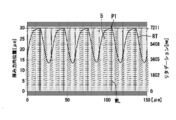
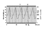
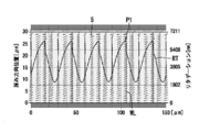
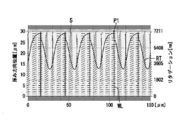
- FIGS. 12 and 17 scales are shown on the horizontal axis and the vertical axis.
- the horizontal axis indicates the position ( ⁇ m) of the second direction D2 in the liquid crystal element 100.
- the vertical axis indicates the position ( ⁇ m: position in the thickness direction) of the first direction D1 in the liquid crystal layer LQ of the liquid crystal element 100.
- the scales of the horizontal axis and the left vertical axis are the same as the scales of the horizontal axis and the vertical axis shown in FIG. 12, respectively. Further, in FIGS.
- the scales of the horizontal axis and the left vertical axis are the same as the scales of the horizontal axis and the vertical axis shown in FIG. 17, respectively.
- the scale on the horizontal axis is the same as the scale on the horizontal axis shown in FIG.
- the scale on the left vertical axis shows 0 ⁇ m to 15 ⁇ m, which is different from the scale on the horizontal axis shown in FIG. 17 (0 ⁇ m to 30 ⁇ m).
- the vertical axis on the right side indicates retardation (nm).
- liquid crystal molecule 5 is indicated by a “short line segment”.
- Examples 1 to 3 The liquid crystal element 100 according to Examples 1 to 3 and the liquid crystal element according to Comparative Example 1 of the present invention will be described with reference to FIGS. 12 to 16.
- FIG. 12 is a cross-sectional view showing a liquid crystal element 100 according to an embodiment of the present invention. As shown in FIG. 12, the configuration of the liquid crystal element 100 according to the present embodiment is the same as the configuration of the liquid crystal element 100 according to the first embodiment described with reference to FIG. 1 (a).
- the first voltage V1 applied to the first electrode 1 was 0.5 V (effective value).
- the second voltage V2 applied to the second electrode 2 was 3.0 V (effective value).
- the pre-twist angle of the alignment film AF1 and the alignment film AF2 was 45 degrees (see FIG. 3A).
- the pretilt angle was 0.1 degrees.
- the thickness d of the liquid crystal layer LQ was 30 ⁇ m.
- the width dw of the unit electrode 10 was 23 ⁇ m.
- the width of each of the first electrode 1 and the second electrode 2 was 10 ⁇ m.
- the thickness t of the wall portion WL was 1 ⁇ m.
- the anchoring energy of the wall WL was 1 ⁇ 10 30 (J / m 2 ).
- Example 1 the retardation RT was calculated by simulation under the conditions of the liquid crystal element 100 of FIG.
- the liquid crystal element according to Comparative Example 1 had a configuration in which the wall portion WL was removed from the liquid crystal element 100 of FIG. Comparative Example 1 and Examples 1 to 3 will be described with reference to FIGS. 13 to 16.
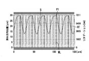
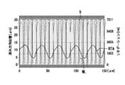
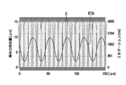
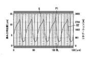
- FIG. 13 shows the retardation RTA of the liquid crystal element according to Comparative Example 1. As shown in FIG. 13, in the liquid crystal device according to Comparative Example 1, the amplitude difference of the retardation RTA was about 2200 (nm).
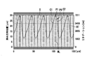
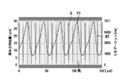
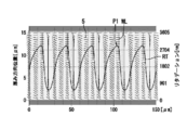
- FIG. 14 shows the retardation RT of the liquid crystal element 100 according to the first embodiment.
- the material of the wall WL was an electrical insulator.
- the amplitude difference of the retardation RT was about 5000 (nm). Therefore, in Example 1, the attenuation of the amplitude difference of the retardation RT could be suppressed as compared with Comparative Example 1.
- the convex portion PR of the retardation RT had a gently inclined portion C1 and a steeply inclined portion C2.
- the retardation RT had a shape that repeated a substantially inverted N-shape.
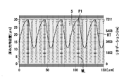
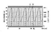
- FIG. 15 shows the retardation RT of the liquid crystal element 100 according to the second embodiment.
- the material of the wall portion WL was a high resistor.
- the amplitude difference of the retardation RT was about 4300 (nm). Therefore, in Example 2, the attenuation of the amplitude difference of the retardation RT could be suppressed as compared with Comparative Example 1.
- FIG. 16 shows the retardation RT of the liquid crystal element 100 according to the third embodiment.
- the material of the wall portion WL was an electric conductor.
- the amplitude difference of the retardation RT was about 4300 (nm). Therefore, in Example 3, the attenuation of the amplitude difference of the retardation RT could be suppressed as compared with Comparative Example 1.
- the wall part WL suppresses the attenuation of the amplitude difference of the wavy retardation RT without depending on the electrical resistivity of the wall part WL. It was.
- the shapes of the retardation RTs of Examples 2 and 3 had the same characteristics as the shapes of the retardation RTs of Example 1.
- Example 4 The liquid crystal element 100 according to Examples 4 to 7 and the liquid crystal element according to Comparative Example 1 of the present invention will be described with reference to FIGS. 17 to 22.
- FIG. 17 is a cross-sectional view showing a liquid crystal element 100 according to an embodiment of the present invention. As shown in FIG. 17, the configuration of the liquid crystal element 100 according to the present embodiment was the same as the configuration of the liquid crystal element 100G according to the second embodiment described with reference to FIG.
- the liquid crystal element 100 shown in FIG. 17 includes a plurality of high resistance layers 30 in addition to the configuration of the liquid crystal element 100 shown in FIG.
- the conditions of the liquid crystal element 100 shown in FIG. 17 were the same as the conditions of the liquid crystal element 100 shown in FIG. 12, except for the high resistance layer 30.
- the anchoring energy of the wall WL was 1 ⁇ 10 30 (J / m 2 ).
- the retardation RT was calculated by simulation under the conditions of the liquid crystal element 100 of FIG.
- the liquid crystal element according to Comparative Example 2 had a configuration in which the wall portion WL was removed from the liquid crystal element 100 of FIG.
- the first voltage V1 applied to the first electrode 1 was 0.5 V (effective value).
- the second voltage V2 applied to the second electrode 2 was 3.0 V (effective value).
- Example 7 the first voltage V1 applied to the first electrode 1 was 3.0 V (effective value).
- the second voltage V2 applied to the second electrode 2 was 0.5 V (effective value).
- FIG. 18 shows the retardation RTA of the liquid crystal element according to Comparative Example 2. As shown in FIG. 18, in the liquid crystal device according to Comparative Example 2, the amplitude difference of the retardation RTA was about 1800 (nm).
- FIG. 19 shows the retardation RT of the liquid crystal element 100 according to the fourth embodiment.
- the material of the wall portion WL was an electrical insulator.
- the amplitude difference of the retardation RT was about 5000 (nm). Therefore, in Example 4, when the liquid crystal element 100 has the high resistance layer 30, the attenuation of the amplitude difference of the retardation RT can be suppressed as compared with Comparative Example 2.
- the convex portion PR of the retardation RT had a gently inclined portion C1 and a steeply inclined portion C2.
- the retardation RT had a shape that repeated a substantially inverted N-shape.
- FIG. 20 shows the retardation RT of the liquid crystal element 100 according to the fifth embodiment.
- the material of the wall WL was a high resistor.
- the amplitude difference of the retardation RT was about 4500 (nm). Therefore, in Example 5, when the liquid crystal element 100 has the high resistance layer 30, the attenuation of the amplitude difference of the retardation RT can be suppressed as compared with Comparative Example 2.
- FIG. 21 shows the retardation RT of the liquid crystal element 100 according to the sixth embodiment.
- the material of the wall portion WL was an electric conductor.
- the amplitude difference of the retardation RT was about 4000 (nm). Therefore, in Example 6, when the liquid crystal element 100 has the high resistance layer 30, the attenuation of the amplitude difference of the retardation RT can be suppressed as compared with Comparative Example 2.
- the wall portion WL does not depend on the electrical resistivity of the wall portion WL.
- the attenuation of the amplitude difference of the wavy retardation RT was suppressed.
- the shapes of the retardation RTs of Examples 5 and 6 had the same characteristics as the shapes of the retardation RTs of Example 4.
- FIG. 22 shows the retardation RT of the liquid crystal element 100 according to the seventh embodiment.
- the seventh embodiment is different from the fourth embodiment in that the first voltage V1 is larger than the second voltage V2 and the first voltage V1 is smaller than the second voltage V2.
- the material of the wall portion WL was an electric insulator as in Example 4.
- the amplitude difference of the retardation RT was about 5000 (nm). Therefore, in Example 7, when the liquid crystal element 100 has the high resistance layer 30, the attenuation of the amplitude difference of the retardation RT can be suppressed as compared with Comparative Example 2.
- Example 8 to 11 The liquid crystal element 100 according to the eighth to eleventh embodiments of the present invention will be described with reference to FIGS. 23 to 26.
- the retardation RT was calculated by simulation under the conditions of the liquid crystal element 100 of FIG.
- the first voltage V1 was 0.5 V (effective value)
- the second voltage V2 was 3.0 V (effective value).
- the anchoring energy of the wall portion WL was set to be smaller than the anchoring energy of the wall portion WL of Examples 4 to 6.
- FIG. 23 shows the retardation RT of the liquid crystal element 100 according to the eighth embodiment.
- the wall portion WL was composed of an electric insulator, and the anchoring energy of the wall portion WL was 1 ⁇ 10 -6 (J / m 2 ).
- the amplitude difference of the retardation RT was about 3500 (nm). Therefore, in Example 8, when the wall portion WL is an electric insulator, even if the anchoring energy is 1 ⁇ 10 -6 (J / m 2 ), the attenuation is as opposed to Comparative Example 2 (FIG. 18). The attenuation of the RT amplitude difference could be suppressed.
- FIG. 24 shows the retardation RT of the liquid crystal element 100 according to the ninth embodiment.
- the wall portion WL was composed of an electric insulator, and the anchoring energy of the wall portion WL was 1 ⁇ 10 -5 (J / m 2 ).
- the amplitude difference of the retardation RT was about 5400 (nm). Therefore, in Example 9, when the wall portion WL is an electrical insulator, even when the anchoring energy of the wall portion WL is 1 ⁇ 10 -5 (J / m 2 ), Comparative Example 2 (FIG. 18) shows. On the other hand, the attenuation of the amplitude difference of the retardation RT could be suppressed.
- the fourth embodiment has an anchoring energy of 1 ⁇ 10 30 (J / m 2 ).
- An amplitude difference of the retardation RT similar to that in FIG. 19 could be secured.
- a sufficient amplitude difference of the retardation RT can be secured by setting the anchoring energy of the wall portion WL to 1 ⁇ 10 -5 (J / m 2 ) or more.
- FIG. 25 shows the retardation RT of the liquid crystal element 100 according to the tenth embodiment.
- the wall portion WL was composed of a high resistor, and the anchoring energy of the wall portion WL was 1 ⁇ 10 -6 (J / m 2 ).
- the amplitude difference of the retardation RT was about 3600 (nm). Therefore, in Example 10, when the wall portion WL is a high resistor, even when the anchoring energy of the wall portion WL is 1 ⁇ 10 -6 (J / m 2 ), in Comparative Example 2 (FIG. 18). On the other hand, the attenuation of the amplitude difference of the retardation RT could be suppressed.
- FIG. 26 shows the retardation RT of the liquid crystal element 100 according to the eleventh embodiment.
- the wall portion WL was composed of an electric conductor, and the anchoring energy of the wall portion WL was 1 ⁇ 10 -6 (J / m 2 ).
- the amplitude difference of the retardation RT was about 3600 (nm). Therefore, in Example 11, when the wall portion WL is an electric conductor, even when the anchoring energy of the wall portion WL is 1 ⁇ 10 -6 (J / m 2 ), in Comparative Example 2 (FIG. 18). On the other hand, the attenuation of the amplitude difference of the retardation RT could be suppressed.
- the anchoring energy of the wall portion WL is set to 1 ⁇ 10 -5 (J / m 2 ) or more as in the case of Example 9.
- the amplitude difference of the wavy retardation RT is attenuated by the wall portion WL without depending on the electrical resistivity of the wall portion WL. Is suppressed.
- Example 12 to 14 The liquid crystal element 100 according to Examples 12 to 14 of the present invention will be described with reference to FIGS. 27 (a) to 29.
- Example 12 includes Example 12A and Example 12B.
- the retardation RT was calculated by simulation under the conditions of the liquid crystal element 100 of FIG.
- Example 12 the position of the wall portion WL was different from the position of the wall portion WL of Examples 4 to 6.
- Example 12A Example 13, and Example 14, the first voltage V1 was 0.5V (effective value), and the second voltage V2 was 3.0V (effective value).
- Example 12B the first voltage V1 was 3.0 V (effective value), and the second voltage V2 was 0.5 V (effective value).
- Example 12A and Example 12B the wall portion WL was composed of an electric insulator, and the wall portion WL faced the region 92 (FIG. 17) between the unit electrodes 10 adjacent to each other. That is, the configuration of the liquid crystal element 100 according to the twelfth embodiment was a configuration in which a plurality of high resistance layers 30 shown in FIG. 9 were added to the configuration of the liquid crystal element 100B shown in FIG. 4A.
- FIG. 27A shows the retardation RT (V1 ⁇ V2) of the liquid crystal element 100 according to Example 12A.
- FIG. 27B shows the retardation RT (V1> V2) of the liquid crystal element 100 according to the 12B embodiment.
- the amplitude difference of the retardation RT was about 5400 (nm). Therefore, in Example 12A and Example 12B, even when the wall portion WL faces the region 92, the attenuation of the amplitude difference of the retardation RT can be suppressed as compared with Comparative Example 2 (FIG. 18).
- the convex portion PR of the retardation RT of Example 12A had a steeply inclined portion C3 and a gently inclined portion C4.
- the retardation RT of Example 12A had a shape that repeated a substantially N-shape.
- the convex portion PR of the retardation RT of Example 12B had a gently inclined portion C1 and a steeply inclined portion C2.
- the retardation RT of Example 12B had a shape that repeated a substantially inverted N-shape.
- FIG. 28 shows the retardation RT of the liquid crystal element 100 according to the thirteenth embodiment.
- the wall portion WL was formed of an electric insulator, and the wall portion WL faced the first electrode 1 (FIG. 17). That is, the configuration of the liquid crystal element 100 according to the thirteenth embodiment is a configuration in which a plurality of high resistance layers 30 shown in FIG. 9 are added to the configuration of the liquid crystal element 100C shown in FIG.
- the amplitude difference of the retardation RT was about 5400 (nm). Therefore, in Example 13, even when the wall portion WL faces the first electrode 1, the attenuation of the amplitude difference of the retardation RT can be suppressed as compared with Comparative Example 2 (FIG. 18).
- the convex portion PR of the retardation RT had a steeply inclined portion C3 and a gently inclined portion C4.
- the retardation RT had a shape that repeated a substantially N-shape.
- FIG. 29 shows the retardation RT of the liquid crystal element 100 according to the fourteenth embodiment.
- the wall portion WL was formed of an electric insulator, and the wall portion WL faced the second electrode 2 (FIG. 17). That is, the configuration of the liquid crystal element 100 according to the 14th embodiment is a configuration in which a plurality of high resistance layers 30 shown in FIG. 9 are added to the configuration of the liquid crystal element 100D shown in FIG.
- the amplitude difference of the retardation RT was about 4500 (nm). Therefore, in Example 14, even when the wall portion WL faces the second electrode 2, the attenuation of the amplitude difference of the retardation RT can be suppressed as compared with Comparative Example 2 (FIG. 18).
- the convex portion PR of the retardation RT had a gently sloping portion C1 and a steeply sloping portion C2.
- the retardation RT had a shape that repeated a substantially inverted N-shape.
- the wall portion WL is composed of a high resistor and an electric conductor, as in the 12th to 14th embodiments, the wall portion WL does not depend on the position of the wall portion WL, and is compared with the comparative example 2. , It could be easily estimated that the attenuation of the amplitude difference of the retardation RT could be suppressed. This is because, as is clear from Examples 4 to 6 of FIGS. 19 to 21, the amplitude difference of the wavy retardation RT is attenuated by the wall portion WL without depending on the electrical resistivity of the wall portion WL. Is suppressed.
- Example 15 to 17 The liquid crystal element 100 according to Examples 15 to 17 of the present invention will be described with reference to FIGS. 30 to 32.
- the retardation RT was calculated by simulation under the conditions of the liquid crystal element 100 of FIG.
- the first voltage V1 was 0.5 V (effective value)
- the second voltage V2 was 3.0 V (effective value).
- FIG. 30 shows the retardation RT of the liquid crystal element 100 according to the fifteenth embodiment.
- the wall portion WL was composed of an electric insulator, and the pre-twist angle by the alignment film AF1 and the alignment film AF2 was 0 degrees (see FIG. 3B).
- the amplitude difference of the retardation RT was about 4500 (nm). Therefore, in Example 15, even when the pre-twist angle was 0 degrees, the attenuation of the amplitude difference of the retardation RT could be suppressed as compared with Comparative Example 2 (FIG. 18).
- FIG. 31 shows the retardation RT of the liquid crystal element 100 according to the sixteenth embodiment.
- the wall portion WL was composed of an electric insulator, and the pre-twist angle by the alignment film AF1 and the alignment film AF2 was 90 degrees (see FIG. 3C).
- the amplitude difference of the retardation RT was about 5500 (nm). Therefore, in Example 16, even when the pre-twist angle was 90 degrees, the attenuation of the amplitude difference of the retardation RT could be suppressed as compared with Comparative Example 2 (FIG. 18).
- FIG. 32 shows the retardation RT of the liquid crystal element 100 according to the seventeenth embodiment.
- the wall portion WL was composed of an electric insulator
- the pre-twist angle by the alignment film AF2 was 0 degrees
- the pre-twist angle by the alignment film AF1 was 90 degrees (see FIG. 3D). ..
- the amplitude difference of the retardation RT was about 5400 (nm). Therefore, in Example 17, even when the liquid crystal molecules 5 are twisted between the interface BF1 and the interface BF2 of the liquid crystal layer LQ, the attenuation of the amplitude difference of the retardation RT is reduced with respect to Comparative Example 2 (FIG. 18). I was able to suppress it.
- Example 18 The liquid crystal element 100 and Comparative Example 3 according to Examples 18 and 19 of the present invention will be described with reference to FIGS. 33 to 35.
- the retardation RT was calculated by simulation under the conditions of the liquid crystal element 100 of FIG.
- the first voltage V1 was 0.5 V (effective value)
- the second voltage V2 was 3.0 V (effective value).
- Example 18 Example 19, and Comparative Example 3
- the thickness d of the liquid crystal layer LQ was 15 ⁇ m.
- the length of the wall portion WL was made different from that of Examples 4 to 6.
- the liquid crystal element according to Comparative Example 3 did not have a wall portion WL.
- FIG. 33 shows the retardation RT of the liquid crystal element according to Comparative Example 3. As shown in FIG. 33, in the liquid crystal device according to Comparative Example 3, the amplitude difference of the retardation RTA was about 1800 (nm).
- FIG. 34 shows the retardation RT of the liquid crystal element 100 according to the eighteenth embodiment.
- the wall portion WL extends from the side of the counter electrode 20 toward the side of the plurality of unit electrodes 10, and the length L of the wall portion WL is 6 ⁇ m. That is, the configuration of the liquid crystal element 100 according to Example 18 was a configuration in which a plurality of high resistance layers 30 shown in FIG. 9 were added to the configuration of the liquid crystal element 100E shown in FIG. 7.
- the amplitude difference of the retardation RT was about 2600 (nm). Therefore, in Example 18, even when the length L of the wall portion WL was 6 ⁇ m, the attenuation of the amplitude difference of the retardation RT could be suppressed as compared with Comparative Example 3.
- FIG. 35 shows the retardation RT of the liquid crystal element 100 according to the nineteenth embodiment.
- the wall portion WL extends from the side of the plurality of unit electrodes 10 toward the side of the counter electrode 20, and the length L of the wall portion WL is 6 ⁇ m. That is, the configuration of the liquid crystal element 100 according to the nineteenth embodiment is a configuration in which a plurality of high resistance layers 30 shown in FIG. 9 are added to the configuration of the liquid crystal element 100F shown in FIG.
- the amplitude difference of the retardation RT was about 2500 (nm). Therefore, in Example 19, even when the length of the wall portion WL was 6 ⁇ m, the attenuation of the amplitude difference of the retardation RT could be suppressed as compared with Comparative Example 3.
- the following (1) to (5) can be easily estimated from the analogies of Examples 4 to 19.
- the characteristics of the retardation RT of the liquid crystal layer LQ according to Examples 1 to 3 having no high resistance layer 30 are the characteristics of the retardation RT of the liquid crystal layer LQ according to Examples 4 to 6 having the high resistance layer 30. Because it was the same.
- Attenuation of the amplitude difference of the retardation RT can be suppressed without depending on the magnitude relationship between the first voltage V1 and the second voltage V2.
- the anchoring energy of the wall portion WL is set to 1 ⁇ 10 -5 (J / m 2 ) or more.
- Attenuation of the amplitude difference of the retardation RT can be suppressed without depending on the position of the wall portion WL.
- Attenuation of the amplitude difference of the retardation RT can be suppressed without depending on the pre-twist angle.
- Attenuation of the amplitude difference of the retardation RT can be suppressed without depending on the extending direction of the wall portion WL.
- the present invention has been described above with reference to the drawings. However, the present invention is not limited to the above-described embodiment, and can be implemented in various aspects without departing from the gist thereof.
- the plurality of components disclosed in the above embodiment can be appropriately modified. For example, one component of all components shown in one embodiment may be added to another component of another embodiment, or some component of all components shown in one embodiment. The element may be removed from the embodiment.
- the present invention provides a liquid crystal element and has industrial applicability.
Landscapes
- Physics & Mathematics (AREA)
- Nonlinear Science (AREA)
- General Physics & Mathematics (AREA)
- Optics & Photonics (AREA)
- Mathematical Physics (AREA)
- Chemical & Material Sciences (AREA)
- Crystallography & Structural Chemistry (AREA)
- Geometry (AREA)
- Spectroscopy & Molecular Physics (AREA)
- Liquid Crystal (AREA)
Abstract
液晶素子(100)は、複数の単位電極(10)と、液晶層(LQ)と、複数の壁部(WL)とを備える。複数の単位電極(10)の各々が第1電極(1)および第2電極(2)を含む。液晶層(LQ)には、複数の単位電極(10)の各々から電圧が印加される。複数の壁部(WL)は、液晶層(LQ)に配置される。液晶層(LQ)は、波状のリタデーション(RT)を有する。リタデーション(RT)の複数のピーク(P1)のうちの2以上のピーク(P1)は、それぞれ、複数の壁部(WL)の位置に対応する。
Description
本発明は、液晶素子に関する。
特許文献1に記載された液晶レンズアレイは、パターン電極層、グランド電極層、液晶層、および、立設部を備える。パターン電極層は、第1パターン電極層と、第2パターン電極層とからなる。立設部は、グランド電極層を有する基板からパターン電極層に向かって液晶層の内部へと突出している。立設部は導電性を有する。また、特許文献1では、好ましい例として、立設部の表面が弱アンカリング面であることが記載されている。弱アンカリング面とは、液晶層を構成する配向膜の面よりも液晶分子に対する束縛力(配向規制力)が弱い面のことである。
液晶レンズアレイでは、立設部によって、高電位側の電極からの漏れ電界の影響がシールドされるため、低電位側の電極の電位が実効的に高くならない。従って、光学位相差の最大値が増加し、偏向角が増大するとともに光学位相差(リタデーションに相当)が直線状に近くなる。
しかしながら、特許文献1に記載された液晶レンズアレイでは、立設部と光学位相差との関係が明らかではない。例えば、光学位相差の最小値は、互いに隣り合う立設部のうちの一方の立設部に対応して位置し、光学位相差の最大値は、他方の立設部に対応して位置すると考えられ得る。
一方、本願の発明者は、鋭意研究によって、波状のリタデーションを有する液晶素子において、第1電極と第2電極とから構成される単位電極の幅が狭くなると、幅の狭い単位電極に対応して、波状のリタデーションの振幅差が減衰することを見出した。
本発明の目的は、波状のリタデーションの振幅差の減衰を抑制できる液晶素子を提供することにある。
本発明の一局面によれば、液晶素子は、複数の単位電極と、液晶層と、複数の壁部とを備える。複数の単位電極の各々が第1電極および第2電極を含む。液晶層には、前記複数の単位電極の各々から電圧が印加される。複数の壁部は、前記液晶層に配置される。前記液晶層は、波状のリタデーションを有する。前記リタデーションの複数のピークのうちの2以上のピークは、それぞれ、前記複数の壁部の位置に対応する。
本発明の液晶素子において、前記壁部の壁面は、高分子によって構成されるか、極性部位を有する物質によって構成されるか、または、極性部位を有する高分子によって構成されることが好ましい。
本発明の液晶素子において、前記液晶層を構成する液晶分子のうち前記壁部に接触している液晶分子のダイレクターは、前記液晶層の界面に沿った方向を向いていることが好ましい。
本発明の液晶素子において、前記壁部のアンカリングエネルギーは、1×10⁻⁶(J/m2)以上であることが好ましい。
本発明の液晶素子において、前記壁部は、前記単位電極を構成する前記第1電極と前記第2電極との間の領域に対向することが好ましい。
本発明の液晶素子において、前記壁部は、前記単位電極と前記単位電極との間の領域に対向することが好ましい。
本発明の液晶素子において、前記壁部は、前記第1電極と前記第2電極とのうちのいずれかに対向することが好ましい。
本発明の液晶素子において、前記壁部は、前記液晶層の一方の界面の側から他方の界面の側まで延びていることが好ましい。
本発明の液晶素子において、前記複数の単位電極は、光軸に対して同心円状に配置されることが好ましい。前記複数の単位電極の幅は、前記光軸に対する径方向の外側に位置する前記単位電極ほど小さいことが好ましい。前記壁部は、前記複数の単位電極のうち所定位置よりも前記径方向の外側に位置する単位電極に対応して配置されることが好ましい。
本発明によれば、波状のリタデーションの振幅差の減衰を抑制できる液晶素子を提供できる。
以下、本発明の実施形態について、図面を参照しながら説明する。なお、図中、同一または相当部分については同一の参照符号を付して説明を繰り返さない。また、本発明の実施形態において、図面の理解を容易にするために、三次元直交座標系のX軸、Y軸、およびZ軸を適宜付記している。なお、図面の簡略化のため、断面を示す斜線を適宜省略する。
(実施形態1)
図1(a)~図3(d)を参照して、本発明の実施形態1に係る液晶素子100について説明する。液晶素子100は、例えば、液晶レンズとして機能することができる。例えば、液晶レンズとして機能する液晶素子100は、光学機器のレンズに採用できる。光学機器は、例えば、眼鏡、ヘッドマウントディスプレイ、内視鏡、または、カメラであるが、液晶素子100の適用は特に限定されない。
図1(a)~図3(d)を参照して、本発明の実施形態1に係る液晶素子100について説明する。液晶素子100は、例えば、液晶レンズとして機能することができる。例えば、液晶レンズとして機能する液晶素子100は、光学機器のレンズに採用できる。光学機器は、例えば、眼鏡、ヘッドマウントディスプレイ、内視鏡、または、カメラであるが、液晶素子100の適用は特に限定されない。
図1(a)は、液晶素子100を示す断面図である。図1(a)に示すように、液晶素子100は、基板SB1と、複数の単位電極10と、絶縁層LRと、配向膜AF1と、液晶層LQと、配向膜AF2と、対向電極20と、複数の壁部WLと、基板SB2とを備える。対向電極20は、「電極」の一例に相当する。
基板SB1と基板SB2との間に、複数の単位電極10、絶縁層LR、配向膜AF1、液晶層LQ、配向膜AF2、対向電極20、および、複数の壁部WLが配置される。複数の単位電極10と対向電極20との間に、絶縁層LR、配向膜AF1、液晶層LQ、配向膜AF2、および、複数の壁部WLが配置される。
複数の単位電極10と液晶層LQとの間に、絶縁層LRおよび配向膜AF1が配置される。配向膜AF1は、液晶層LQの界面BF1に配置される。界面BF1は、液晶層LQのうち複数の単位電極10の側の面を示す。絶縁層LRと対向電極20との間に、配向膜AF1、液晶層LQ、配向膜AF2、および、複数の壁部WLが配置される。配向膜AF2は、液晶層LQの界面BF2に配置される。界面BF2は、液晶層LQのうち対向電極20の側の面を示す。界面BF1と界面BF2とは、第1方向D1に対向している。
第1方向D1は、単位電極10および対向電極20に対して略直交する方向を示す。換言すれば、第1方向D1は、液晶層LQの界面BF1および界面BF2に対して略直交する。第1方向D1は、方向Daおよび方向Dbを含む。方向Daは、対向電極20の側から複数の単位電極10の側に向かう方向を示す。方向Dbは、方向Daの反対方向であり、複数の単位電極10の側から対向電極20の側に向かう方向を示す。第2方向D2は、第1方向D1に対して略直交する。換言すれば、第2方向D2は、界面BF1および界面BF2に対して略平行である。
基板SB1は略平板状である。基板SB1は、例えば、透明であり、ガラスまたは合成樹脂により形成される。本明細書において、透明は、無色透明、有色透明、および、半透明を含む。
複数の単位電極10の各々は、同一階層に配置される。複数の単位電極10は互いに間隔をあけて配置される。複数の単位電極10の各々は、第1電極1と、第2電極2とを含む。各単位電極10を構成する第1電極1と第2電極2とは、互いに間隔をあけて配置される。第1電極1および第2電極2の各々は、例えば、透明であり、ITO(インジウム・スズ酸化物:Indium Tin Oxide)により形成される。なお、第1電極1および第2電極2の各々は、例えば、銅等の金属メッシュ、ITOと金属メッシュとの積層構造、または、導電性のカーボンブラック製のファイバーとITOとの積層構造もしくは混合体により形成されていてもよく、素材は特に限定されない。
第1電極1には第1電圧V1が印加される。そして、第1電極1は、液晶層LQに第1電圧V1を印加する。第1電圧V1は交流電圧である。第2電極2には第2電圧V2が印加される。そして、第2電極2は、液晶層LQに第2電圧V2を印加する。第2電圧V2は交流電圧である。第1電圧V1と第2電圧V2とは異なる。実施形態1では、第1電圧V1の実効値と第2電圧V2の実効値とは異なる。第1電圧V1の周波数と第2電圧V2の周波数とは、同じであってもよいし、異なっていてもよい。
絶縁層LRは電気絶縁体である。絶縁層LRは、例えば、透明であり、二酸化ケイ素(SiO2)により形成される。なお、絶縁層LRは、例えば、二酸化ケイ素以外の金属酸化物、または、有機薄膜により形成されていてもよく、素材は特に限定されない。
配向膜AF1は、液晶層LQの液晶分子の配向を定める。配向膜AF1は、例えば、透明であり、ポリイミド膜である。
液晶層LQは液晶によって構成される。従って、液晶層LQは、多数の液晶分子を含む。液晶層LQを構成する液晶は、例えば、ネマティック液晶であり、透明である。また、実施形態1では、液晶の配向は、無電場の環境下において、ホモジニアス配向である。ホモジニアス配向とは、液晶分子のダイレクターが第2方向D2に略平行な状態を示す。なお、液晶の配向は、無電場の環境下において、ホメオトロピック配向であってもよい。ホメオトロピック配向とは、液晶分子のダイレクターが第2方向D2に略垂直な状態を示す。
配向膜AF2は、液晶層LQの液晶分子の配向を定める。配向膜AF2は、例えば、透明であり、ポリイミド膜である。
対向電極20は、絶縁層LRおよび液晶層LQを介して、複数の単位電極10に対向する。対向電極20は略面状の電極である。対向電極20は、例えば、透明であり、ITOにより形成される。対向電極20には第3電圧V3が印加される。そして、対向電極20は液晶層LQに第3電圧V3を印加する。例えば、対向電極20は接地されており、第3電圧V3は接地電位(0V)に設定される。
基板SB2は略平板状である。基板SB2は、例えば、透明であり、ガラスにより形成される。
複数の壁部WLは、液晶層LQに配置される。複数の壁部WLの各々は、第2方向D2に沿って延びている。複数の壁部WLは互いに略平行である。複数の壁部WLは、それぞれ、複数の単位電極10に対向している。壁部WLは、例えば、透明である。壁部WLは、電気絶縁体、高抵抗体、または、電気伝導体によって構成される。本明細書において、高抵抗体の電気抵抗率は、電気伝導体の電気抵抗率より大きく、電気絶縁体の電気抵抗率より小さい。
例えば、高抵抗体の面抵抗は5×10³Ω/□以上5×109Ω/□以下であり、電気伝導体の面抵抗は5×10-1Ω/□以上5×102Ω/□以下であり、電気絶縁体の面抵抗は1×1011Ω/□以上1×1015Ω/□以下である。例えば、高抵抗体の面抵抗は1×102Ω/□以上1×1011Ω/□以下であり、電気伝導体の面抵抗は1×10-2Ω/□以上1×102Ω/□以下であり、電気絶縁体の面抵抗は1×1011Ω/□以上1×1016Ω/□以下であってもよい。なお、これらの例示は、本発明の適用において、高抵抗体の面抵抗、電気伝導体の面抵抗、および、電気伝導体の面抵抗を限定しない。
引き続き図1(a)を参照して、液晶素子100の光学特性を説明する。第1電圧V1が第1電極1に印加され、第2電圧V2が第2電極2に印加され、第3電圧V3が対向電極20に印加された状態では、液晶層LQは、波状のリタデーションRTを有する。「波状」は、大小の極値が交互に繰り返される連続した形状を示す。
以下、第1電圧V1が第1電極1に印加され、第2電圧V2が第2電極2に印加され、第3電圧V3が対向電極20に印加された状態を、「液晶駆動状態」と記載する場合がある。
リタデーションとは、液晶層LQに入射した光が互いに垂直な振動方向を持つ2つの光波(例えば、通常光および異常光)に分かれる現象によって生じる両波の位相差を示す量のことである。リタデーションは、R=△n×dで表される。Rはリタデーション、△nは液晶層LQの複屈折、dは液晶層LQの厚みを示す。Δnは、液晶分子のダイレクターの第2方向D2に対するチルト角によって変化し得る。従って、リタデーションもまた、液晶分子のダイレクターの第2方向D2に対するチルト角によって変化し得る。
例えば、Δn=ne(φ)-no、である。noは、通常光についての屈折率を示す。noは、入射光の光学軸OPに対する角度には依存しない。換言すれば、noは、第2方向D2に対する光学軸OPの傾き角φに依存しない。光学軸OPは、液晶分子の光学軸を示し、光学異方性を有する液晶において、光を入射しても光が分かれない方向のことである。ne(φ)は、異常光についての屈折率を示す。ne(φ)は、入射光の光学軸OPに対する角度によって変化する。換言すれば、ne(φ)は、第2方向D2に対する光学軸OPの傾き角φによって変化する。従って、リタデーションもまた、第2方向D2に対する液晶分子の光学軸OPの傾き角φによって変化する。その結果、例えば、液晶駆動状態の液晶層LQにおいて、あるX座標X1上で第1方向D1(Z方向)に沿って位置している複数の液晶分子(以下、「複数の液晶分子ML1」と記載する場合がある。)の光学軸OPの傾き角φは、他のX座標X2上で第1方向D1(Z方向)に沿って位置している複数の液晶分子(以下、「複数の液晶分子ML2」と記載する場合がある。)の光学軸OPの傾き角φと異なり、X座標X1におけるリタデーションとX座標X2におけるリタデーションとは異なる。なお、この例では、説明の簡略化のために、液晶駆動状態において、X座標X1上の複数の液晶分子ML1の光学軸OPの傾き角φを同一とし、X座標X2上の複数の液晶分子ML2の光学軸OPの傾き角φを同一とした。
例えば、あるX座標X1におけるリタデーションは、次のようにして算出できる。すなわち、液晶層LQにおいて、あるX座標X1上には、複数の液晶分子ML1が、第1方向D1(Z方向)に沿って存在する。そして、実際には、液晶駆動状態において、複数の液晶分子ML1の光学軸OPの傾き角φは、同一ではない。そこで、複数の液晶分子ML1ごとのΔnを、厚み0から厚みdまで積算することで、X座標X1におけるリタデーションを算出する。
なお、例えば、液晶層LQのうち、液晶分子のダイレクターが界面BF1または界面BF2に略直交する液晶部分のリタデーションは、最小になる。例えば、液晶層LQのうち、液晶分子のダイレクターが界面BF1または界面BF2に略平行である液晶部分のリタデーションは、最大になる。
実施形態1では、複数の単位電極10を配置して、第1電極1に第1電圧V1を印加するとともに、第2電極2に第2電圧V2を印加することによって、液晶層LQには、波状のリタデーションRTが発生する。
実施形態1では、図1(a)に示すように、波状のリタデーションRTの複数のピークP1は、それぞれ、複数の壁部WLの位置に対応する。従って、実施形態1によれば、複数の壁部WLを液晶層LQに配置することによって、液晶層LQのうち幅dwの比較的小さな単位電極10に対応する部分においても、波状のリタデーションRTの振幅差(P1-P2)が減衰することを抑制できる。その結果、液晶層LQのうち幅dwの比較的小さな単位電極10に対応する液晶部分においても、比較的大きな光の屈折角を実現できる。
図1(a)の例では、波状のリタデーションRTの複数のピークP1は、それぞれ、複数の壁部WLの位置に位置する。つまり、第2方向D2(X方向)におけるピークP1の位置は、第2方向D2(X方向)における壁部WLの位置と略同じである。ただし、ピークP1は、第2方向D2において壁部WLに近接する位置に位置していてもよい。例えば、「壁部WLに近接する位置」は、第2方向D2において壁部WLに対して間隔DTの±15%の範囲内の位置であり、第2方向D2において壁部WLに対して間隔DTの±10%の範囲内の位置であることが好ましく、第2方向D2において壁部WLに対して間隔DTの±5%の範囲内の位置であることがさらに好ましい。間隔DTは、互いに隣り合う壁部WLと壁部WLとの間の第2方向D2における間隔を示す。なお、第1方向D1(Z方向)におけるピークP1の位置は、特に限定されない。
なお、波状のリタデーションRTの振幅差(P1-P2)が大きい程、光の屈折角は大きくなる一方、波状のリタデーションRTの振幅差(P1-P2)が小さくなる程、光の屈折角は小さくなる。「振幅差」は、波状のリタデーションRTにおいて、ピークP1と、ピークP1の隣の極値P2との差分を示す。
ピークP1は、波状のリタデーションRTの局所的な最大値を示す。従って、複数のピークP1の大きさは、異なっていてもよいし、同じであってもよい。極値P2は、波状のリタデーションRTの局所的な最小値を示す。従って、複数の極値P2の大きさは、異なっていてもよいし、同じであってもよい。
リタデーションRTは、次のようにして測定することができる。例えば、直交偏光子間に液晶素子100を配置する。そして、直交偏光子間の透過スペクトルの測定によって透過率を求めると、透過率からΔnを求めることができる。一方、厚み測定器によって液晶層LQの厚みdを測定する。そして、Δn×dによって、リタデーションを算出する。また、例えば、偏光顕微鏡によって、液晶素子100のクロスニコル観察を行うと、干渉縞がリタデーションRTを表す。
次に、図2を参照して、液晶層LQのリタデーションRTを説明する。図2は、液晶層LQに含まれる液晶分子5の状態を模式的に示す断面図である。図2では、第1電極1に印加する第1電圧V1は、第2電極2に印加する第2電圧V2よりも小さい。なお、図2では、図面の簡略化のため、基板SB1、SB2を省略している。
図2に示すように、液晶層LQは多数の液晶分子5を含む。液晶層LQにおいて、互いに隣り合う壁部WLの間の領域ARでは、液晶分子5yのダイレクターは、第2電圧V2によって、例えば、界面BF1、BF2に対して略直交する。従って、領域ARにおいて、リタデーションRTの極値P2が発生する。
一方、液晶層LQを構成する液晶分子5のうち壁部WLに接触している液晶分子5xのダイレクターは、例えば、液晶層LQの界面BF1および界面BF2に略平行な方向を向いている。つまり、液晶層LQを構成する液晶分子5のうち壁部WLに接触している液晶分子5xのダイレクターは、液晶層LQの界面BF1および界面BF2に沿った方向を向いている。従って、実施形態1によれば、壁部WLの位置において、リタデーションRTのピークP1が大きくなる。その結果、波状のリタデーションRTの振幅差の減衰を抑制できる。
なお、壁部WLが電気伝導体によって構成される場合には、液晶分子5xのダイレクターは、壁部WLと液晶分子5xと電場との相互作用によっても、界面BF1および界面BF2に沿った方向を向くと推定される。
また、壁部WLを設けない場合における波状のリタデーションRTの振幅差よりも、振幅差が大きくなる限りにおいては、壁部WLに接触する液晶分子5xのダイレクターは、界面BF1および界面BF2に対して傾斜する方向を向いていてもよい。
さらに、液晶層LQのうち、互いに隣り合う壁部WLのうちの一方の壁部WL1と領域ARとの間の領域においては、液晶分子5の連続性により、液晶分子5は、壁部WL1から領域ARに向かって、平臥状態から起立状態に徐々に変化する。また、領域ARと他方の壁部WL2との間の領域においても、液晶分子5の連続性により、液晶分子5の配向は、領域ARから壁部WL2に向かって、起立状態から平臥状態に徐々に変化する。その結果、図2に示すように、複数のピークP1および複数の極値P2を有する波状のリタデーションRTが発生する。
特に、実施形態1では、壁部WLは、液晶層LQにおいて対向電極20の側から単位電極10の側まで延びている。従って、液晶層LQにおいて対向電極20の側から単位電極10の側にわたって、壁部WLに接触する液晶分子5xのダイレクターが、界面BF1および界面BF2に沿った方向を向く。その結果、波状のリタデーションRTのピークP1が大きくなって、リタデーションRTの振幅差の減衰を効果的に抑制できる。図2の例では、壁部WLは、液晶層LQの界面BF2から界面BF1まで延びている。
なお、液晶分子5のダイレクターは次のようにして測定できる。例えば、直接的には、偏光ラマン分光法または偏光赤外分光法によって、液晶の配向またはオーダーパラメーターを観測する。例えば、間接的な光学的手法として、屈折率異方性の方向または誘電率異方性を観測する。
また、壁部WLの厚みtは、薄いほど好ましい。液晶層LQを通過する光が、壁部WLから直接影響を受けることを抑制できるからである。壁部WLの厚みtは、第2方向D2における壁部WLの厚みを示す。壁部WLの厚みtは、例えば、第1電極1の幅または第2電極2の幅よりも小さいことが好ましい。壁部WLの厚みtは、例えば、領域90の幅または領域92の幅よりも小さいことが好ましい。壁部WLの厚みtは、例えば、5μm以下であることが好ましく、1μm以下であることがさらに好ましい。
領域90は、絶縁層LRのうち、単位電極10を構成する第1電極1と第2電極2との間の領域を示す。なお、領域90は、空間であってもよい。領域92は、絶縁層LRのうち、互いに隣り合う単位電極10の間の領域を示す。なお、領域92は、空間であってもよい。
さらに、実施形態1では、図1(a)に示すように、波状のリタデーションRTは複数の凸状部分PRを有する。凸状部分PRの各々は、ピークP1に対して非対称である。凸状部分PRの各々は、例えば、非対称の略山形状を示す。また、壁部WLは、配向膜AF1を介して絶縁層LRの領域90と第1方向D1に対向する。従って、第1電極1に印加する第1電圧V1が第2電極2に印加する第2電圧V2よりも小さい場合において、複数の凸状部分PRの各々は、ピークP1を挟んで緩傾斜部分C1と急傾斜部分C2とを含む。緩傾斜部分C1は第1電極1に対応している。急傾斜部分C2は第2電極2に対応している。緩傾斜部分C1の傾斜は、急傾斜部分C2の傾斜よりも緩やかである。第1電圧V1が第2電圧V2よりも小さい場合、リタデーションRTは、例えば、略逆N字形状を繰り返す形状を有している。第1電圧V1が第2電圧V2よりも大きい場合については後述する。
なお、例えば、液晶層LQに対して略垂直に入射した光は、緩傾斜部分C1の側に屈折する。図1(a)では、例えば、液晶層LQに対して略垂直に入射した光は、左斜め上方に向かって屈折する。
さらに、実施形態1では、例えば、第1電圧V1と第2電圧V2との大小関係を切り替えて、液晶レンズとして機能する液晶素子100を凸レンズと凹レンズとの間で切り替える際に、凸レンズの焦点距離(例えば正の値)の大きさと凹レンズの焦点距離(例えば負の値)の大きさとを略一致させることができる。その結果、液晶素子100の利用者または設計者にとって利便性が高い。
なお、図2では、絶縁層LRの領域92の幅は領域90の幅と略同じである。しかしながら、領域92の幅および領域90の幅は特に限定されない。例えば、領域92の幅が領域90の幅よりも小さい場合に、壁部WLを領域90に対向して配置することで、壁部WLを領域92に対向して配置する場合よりも、壁部WLの形成が容易になる。
なお、第1電極1に印加する第1電圧V1が、第2電極2に印加する第2電圧V2よりも大きい場合でも、第1電圧V1が第2電圧V2よりも小さい場合と同様に、波状のリタデーションRTが発生する。この場合も、壁部WLのアンカリングによって、壁部WLに接触する液晶分子5xのダイレクターが界面BF1および界面BF2に沿った方向を向く。従って、壁部WLの位置において、リタデーションRTのピークP1が大きくなる。その結果、波状のリタデーションRTの振幅差の減衰を抑制できる。なお、この場合、液晶層LQにおいて、互いに隣り合う壁部WLの間の、ある領域(以下、「領域AR1」と記載する。)では、液晶分子5yのダイレクターは、第1電圧V1によって、例えば、界面BF1および界面BF2に略直交する方向を向いている。従って、液晶層LQにおいて、互いに隣り合う壁部WLの間の領域AR1では、リタデーションRTの極値P2が発生する。
また、第1電圧V1が第2電圧V2よりも大きい場合でも、壁部WL1と領域AR1との間の液晶分子5の連続性、および、領域AR1と壁部WL2との間の液晶分子5の連続性は、第1電圧V1が第2電圧V2よりも小さい場合と同様である。従って、複数のピークP1および複数の極値P2を有する波状のリタデーションRTが発生する。
図1(b)は、第1電極1に印加する第1電圧V1が第2電極2に印加する第2電圧V2よりも大きい場合のリタデーションRTを示す図である。図1(b)に示すように、第1電圧V1が第2電圧V2よりも大きい場合において、波状のリタデーションRTを構成する複数の凸状部分PRの各々は、ピークP1を挟んで急傾斜部分C3と緩傾斜部分C4とを含む。実施形態1では、壁部WLが、配向膜AF1を介して絶縁層LRの領域90と第1方向D1に対向しているからである。急傾斜部分C3は第1電極1に対応する。緩傾斜部分C4は第2電極2に対応する。緩傾斜部分C4の傾斜は、急傾斜部分C3の傾斜よりも緩やかである。第1電圧V1が第2電圧V2よりも大きい場合、リタデーションRTは、例えば、略N字形状を繰り返す形状を有している。
なお、例えば、液晶層LQに対して略垂直に入射した光は、緩傾斜部分C4の側に屈折する。図1(b)では、例えば、液晶層LQに対して略垂直に入射した光は、右斜め上方に向かって屈折する。
ここで、壁部WLのアンカリングとは、液晶分子5に対する配向規制力または束縛力のことである。つまり、壁部WLのアンカリングは、配向膜のアンカリングと同様に定義される。アンカリングの大きさは、例えば、アンカリングエネルギー(J/m2)によって表される。液晶分子5は、液晶材料と壁部WLの材料とで定まる配向容易軸方向に配向する。そして、アンカリングエネルギーは、配向容易軸方向から液晶分子5を引き離すために要求されるエネルギーである。つまり、アンカリングエネルギーは、液晶分子と配向膜との間で定まるアンカリングエネルギーと同様に定義される。
例えば、壁部WLのアンカリングエネルギーは、1×10⁻⁶(J/m2)以上であることが好ましい。この好ましい例では、壁部WLは、壁部WLに接触する液晶分子5xのダイレクターを界面BF1、BF2に沿った方向に向かせるために十分なアンカリングエネルギーを確保できる。
なお、アンカリングエネルギーは次のようにして測定できる。例えば、アンカリングエネルギーは、一般化表面アンカリングモデルにより導かれる飽和閾値電圧法によって測定できる。
次に、壁部WLの材質を例示する。
例えば、壁部WLの壁面は、高分子によって構成される。従って、高分子鎖によって、壁部WLのアンカリングエネルギー大きくなるため、壁部WLに接触する液晶分子5xは、液晶層LQの界面BF1、BF2に沿って効果的に配向する。その結果、波状のリタデーションRTの振幅差の減衰を効果的に抑制できる。高分子は、例えば、電気絶縁体または高抵抗体である。高分子は、例えば、ポリイミドである。なお、高分子は、例えば、電気伝導体(例えば、導電性高分子)であってもよい。導電性高分子は、例えば、PEDOT:PSS(ポリ(4-スチレンスルホン酸)をドープしたポリ(3、4-エチレンジオキシチオフェン))、または、ポリピロールである。なお、壁部WLの全体が高分子によって構成されてもよいし、壁部WLの壁面だけが高分子によって構成されてよい。例えば、壁部WLが、壁部本体と、壁部本体の表面に形成された高分子膜とによって構成されていてもよい。この場合、壁部本体の材料は、特に限定されない。例えば、壁部本体は、電気絶縁体、高抵抗体、または、電気伝導体であってよい。
例えば、壁部WLの壁面は、極性部位を有する物質によって構成される。従って、極性部位によって、壁部WLのアンカリングエネルギー大きくなるため、壁部WLに接触する液晶分子5xは、液晶層LQの界面BF1、BF2に沿って効果的に配向する。その結果、波状のリタデーションRTの振幅差の減衰を効果的に抑制できる。極性部位を有する物質は、例えば、電気絶縁体または高抵抗体である。極性部位を有する物質は、例えば、ポリイミドである。なお、壁部WLの全体が極性部位を有する物質によって構成されてもよいし、壁部WLの壁面だけが極性部位を有する物質によって構成されてよい。例えば、壁部WLが、壁部本体と、壁部本体の表面に形成された極性部位を有する物質の膜とによって構成されていてもよい。この場合、壁部本体の材料は、特に限定されない。例えば、壁部本体は、電気絶縁体、高抵抗体、または、電気伝導体であってよい。
例えば、壁部WLの壁面は、極性部位を有する高分子によって構成される。従って、極性部位および高分子鎖によって、壁部WLのアンカリングエネルギー大きくなるため、壁部WLに接触する液晶分子5xは、液晶層LQの界面BF1、BF2に沿って効果的に配向する。その結果、波状のリタデーションRTの振幅差の減衰を効果的に抑制できる。極性部位を有する高分子は、例えば、電気絶縁体または高抵抗体である。極性部位を有する高分子は、例えば、ポリイミドである。なお、壁部WLの全体が極性部位を有する高分子によって構成されてもよいし、壁部WLの壁面だけが極性部位を有する高分子によって構成されてよい。例えば、壁部WLが、壁部本体と、壁部本体の表面に形成された極性部位を有する高分子膜とによって構成されていてもよい。この場合、壁部本体の材料は、特に限定されない。例えば、壁部本体は、電気絶縁体、高抵抗体、または、電気伝導体であってよい。
次に、壁部WLの作製方法の一例を説明する。液晶(例えば、ビフェニル系液晶)と光硬化型液晶性モノマーの溶液とに光を照射し、このモノマーを重合させて、高密度の高分子網目構造として壁部WLを形成する。具体的には、液晶・液晶性モノマー溶液をポリイミド配向膜付き基板の間に挟み込むと、液晶とともに細長い分子構造の液晶性モノマーが自発的に配向する。その後、紫外線のパターン露光により照射部に高分子を選択的に析出・硬化させる。その際、紫外線の非照射領域のモノマーは、照射部へと熱拡散または濃度拡散して捕捉されていくため、高分子の凝集体が基板面に成長して、壁部WLとしての高分子壁が構築される。つまり、壁部WLは、光硬化型液晶性モノマーから形成された高分子によって構成される。例えば、壁部WLの内部では、光硬化型液晶性モノマーが揃って並んでいる。従って、壁部WLに接触する液晶分子5は、光硬化型液晶性モノマーの並びに沿って配向する。換言すれば、光硬化型液晶性モノマーの初期配向状態によって、壁部WLに接触する液晶分子5の配向を定めることができる。
なお、例えば、壁部WLは、ナノインプリント・リソグラフィ(例えば、光インプリントまたは熱インプリント)、または、フォトリソグラフィを利用して作製されてもよい。例えば、壁部WLを電気絶縁体で構成する場合には、壁部WLは光重合性樹脂によって形成されてもよい。例えば、壁部WLを電気伝導体で構成する場合には、半導電性樹脂に導電粒子を添加または充填したり、半導電性樹脂にカーボンブラック製のファイバーを分散させたりして、壁部WLを作成する。
また、例えば、壁部WLの表面に対して、特定の処理が実行されていてもよい。特定の処理は、例えば、疎水化処理、親水化処理、または、プラズマ処理である。壁部WLの表面に対して特定の処理を実行することで、分子間相互作用が強くなったり、壁部WLに液晶分子5がしみ込み易くなったりする。その結果、壁部WLに接触する液晶分子5のダイレクターを界面BF1、BF2に沿った方向に向かせるために十分なアンカリングエネルギーを確保できる。
次に、図3(a)~図3(d)を参照して、液晶分子5のプレツイスト角を説明する。プレツイスト角は、液晶分子5を平面視したときに、液晶分子5の長軸が基準線BLに対してなす角度を示す。本明細書において、「平面視」は、第1方向D1から対象を見ることを示す。プレツイスト角は、配向膜AF1、AF2によって定められる。
図3(a)~図3(d)は、壁部WLに接触している液晶分子5の状態を示す図である。図3(a)~図3(d)では、壁部WLおよび液晶分子5を、図2の方向Dzから見ている。
図3(a)に示すように、第1例では、液晶分子5の長軸が基準線BLに対してなすプレツイスト角は、45度である。基準線BLは、壁部WLに略直交する。
図3(b)に示すように、第2例では、液晶分子5の長軸が基準線BLに対してなすプレツイスト角は、0度である。
図3(c)に示すように、第3例では、液晶分子5の長軸が基準線BLに対してなすプレツイスト角は、90度である。
図3(d)に示すように、第4例では、配向膜AF2において液晶分子5の長軸が基準線BLに対してなすプレツイスト角は、0度である。加えて、配向膜AF1において液晶分子5の長軸が基準線BLに対してなすプレツイスト角は、90度である。従って、複数の液晶分子5は、配向膜AF1と配向膜AF2との間で捻じれるように配列する。
本発明は、液晶分子5のプレツイスト角に依存することなく適用できる。なぜなら、リタデーションRTは、液晶分子5のダイレクターが液晶層LQの界面BF1、BF2に沿った方向(界面BF1、BF2に平行な方向)に近づく程大きくなる一方、液晶分子5のプレツイスト角には依存しないからである。例えば、壁部WLに接触している液晶分子5xのダイレクターが液晶層LQの界面BF1、BF2沿った方向を向いている限りは、液晶分子5のプレツイスト角に依存することなく、波状のリタデーションRTの振幅差の減衰を抑制できる。
次に、図4(a)~図8を参照して、実施形態1の第1変形例~第5変形例を説明する。第1変形例~第3変形例では、壁部WLの配置が図1および図2を参照して説明した実施形態1と主に異なる。第4変形例および第5変形例では、壁部WLの長さが図1および図2を参照して説明した実施形態1と主に異なる。以下、第1変形例~第5変形例が実施形態1と異なる点を主に説明する。
(第1変形例)
図4(a)は、第1変形例に係る液晶素子100Bを示す断面図である。図4(a)に示すように、第1変形例では、壁部WLは、配向膜AF1を介して、互いに隣り合う単位電極10と単位電極10との間の領域92と第1方向D1に対向する。従って、第1電極1に印加する第1電圧V1が第2電極2に印加する第2電圧V2よりも小さい場合において、波状のリタデーションRTを構成する複数の凸状部分PRの各々は、ピークP1を挟んで急傾斜部分C3と緩傾斜部分C4とを含む。つまり、凸状部分PRは、実施形態1の図1(a)に示す凸状部分PRを左右反転した形状を有する。第1電圧V1が第2電圧V2よりも小さい場合、リタデーションRTは、例えば、略N字形状を繰り返す形状を有している。
図4(a)は、第1変形例に係る液晶素子100Bを示す断面図である。図4(a)に示すように、第1変形例では、壁部WLは、配向膜AF1を介して、互いに隣り合う単位電極10と単位電極10との間の領域92と第1方向D1に対向する。従って、第1電極1に印加する第1電圧V1が第2電極2に印加する第2電圧V2よりも小さい場合において、波状のリタデーションRTを構成する複数の凸状部分PRの各々は、ピークP1を挟んで急傾斜部分C3と緩傾斜部分C4とを含む。つまり、凸状部分PRは、実施形態1の図1(a)に示す凸状部分PRを左右反転した形状を有する。第1電圧V1が第2電圧V2よりも小さい場合、リタデーションRTは、例えば、略N字形状を繰り返す形状を有している。
図4(b)は、第1電極1に印加する第1電圧V1が第2電極2に印加する第2電圧V2よりも大きい場合のリタデーションRTを示す図である。図4(b)に示すように、第1電圧V1が第2電圧V2よりも大きい場合において、波状のリタデーションRTを構成する複数の凸状部分PRの各々は、ピークP1を挟んで緩傾斜部分C1と急傾斜部分C2とを含む。つまり、凸状部分PRは、実施形態1の図1(b)に示す凸状部分PRを左右反転した形状を有する。第1電圧V1が第2電圧V2よりも大きい場合、リタデーションRTは、例えば、略逆N字形状を繰り返す形状を有している。
(第2変形例)
図5は、第2変形例に係る液晶素子100Bを示す断面図である。図5に示すように、第2変形例では、壁部WLは、配向膜AF1を介して、第1電極1と第1方向D1に対向する。加えて、第1電極1に印加する第1電圧V1が第2電極2に印加する第2電圧V2よりも小さい。従って、波状のリタデーションRTを構成する複数の凸状部分PRの各々は、ピークP1を挟んで急傾斜部分C3と緩傾斜部分C4とを含む。第1電圧V1が第2電圧V2よりも小さい場合、リタデーションRTは、例えば、略N字形状を繰り返す形状を有している。
図5は、第2変形例に係る液晶素子100Bを示す断面図である。図5に示すように、第2変形例では、壁部WLは、配向膜AF1を介して、第1電極1と第1方向D1に対向する。加えて、第1電極1に印加する第1電圧V1が第2電極2に印加する第2電圧V2よりも小さい。従って、波状のリタデーションRTを構成する複数の凸状部分PRの各々は、ピークP1を挟んで急傾斜部分C3と緩傾斜部分C4とを含む。第1電圧V1が第2電圧V2よりも小さい場合、リタデーションRTは、例えば、略N字形状を繰り返す形状を有している。
(第3変形例)
図6は、第3変形例に係る液晶素子100Dを示す断面図である。図6に示すように、第3変形例では、壁部WLは、配向膜AF1を介して、第2電極2と第1方向D1に対向する。加えて、第1電極1に印加する第1電圧V1が第2電極2に印加する第2電圧V2よりも小さい。従って、波状のリタデーションRTを構成する複数の凸状部分PRの各々は、ピークP1を挟んで緩傾斜部分C1と急傾斜部分C2とを含む。第1電圧V1が第2電圧V2よりも大きい場合、リタデーションRTは、例えば、略逆N字形状を繰り返す形状を有している。
図6は、第3変形例に係る液晶素子100Dを示す断面図である。図6に示すように、第3変形例では、壁部WLは、配向膜AF1を介して、第2電極2と第1方向D1に対向する。加えて、第1電極1に印加する第1電圧V1が第2電極2に印加する第2電圧V2よりも小さい。従って、波状のリタデーションRTを構成する複数の凸状部分PRの各々は、ピークP1を挟んで緩傾斜部分C1と急傾斜部分C2とを含む。第1電圧V1が第2電圧V2よりも大きい場合、リタデーションRTは、例えば、略逆N字形状を繰り返す形状を有している。
(第4変形例)
図7は、第4変形例に係る液晶素子100Eを示す断面図である。図7に示すように、壁部WLの長さLは、液晶層LQの厚みdよりも短い。長さLは、壁部WLの第1方向D1の長さを示す。壁部WLは、対向電極20の側から複数の単位電極10の側に向かって方向Daに延びている。壁部WLは単位電極10に対向している。具体的には、壁部WLは領域90に対向している。
図7は、第4変形例に係る液晶素子100Eを示す断面図である。図7に示すように、壁部WLの長さLは、液晶層LQの厚みdよりも短い。長さLは、壁部WLの第1方向D1の長さを示す。壁部WLは、対向電極20の側から複数の単位電極10の側に向かって方向Daに延びている。壁部WLは単位電極10に対向している。具体的には、壁部WLは領域90に対向している。
第4変形例では、壁部WLの長さLを短くすることで、液晶層LQを通過する光が、壁部WLから直接影響を受けることを抑制できる。
(第5変形例)
図8は、第5変形例に係る液晶素子100Fを示す断面図である。図8に示すように、壁部WLの長さLは、液晶層LQの厚みdよりも短い。長さLは、壁部WLの第1方向D1の長さを示す。壁部WLは、複数の単位電極10の側から対向電極20の側に向かって方向Dbに延びている。壁部WLは単位電極10に対向している。具体的には、壁部WLは領域90に対向している。
図8は、第5変形例に係る液晶素子100Fを示す断面図である。図8に示すように、壁部WLの長さLは、液晶層LQの厚みdよりも短い。長さLは、壁部WLの第1方向D1の長さを示す。壁部WLは、複数の単位電極10の側から対向電極20の側に向かって方向Dbに延びている。壁部WLは単位電極10に対向している。具体的には、壁部WLは領域90に対向している。
第5変形例では、壁部WLの長さLを短くすることで、液晶層LQを通過する光が、壁部WLから直接影響を受けることを抑制できる。
なお、第4変形例および第5変形例において、壁部WLは、領域92、第1電極1、または、第2電極2に対向していてもよい。
実施形態1および第1変形例~第5変形例において、液晶素子100、100A~100Fは、絶縁層LRに代えて、高抵抗体から構成される高抵抗層(抵抗層)を備えていてもよい。また、液晶素子100、100A~100Fが、単位電極10、液晶層LQ、および、壁部WLを備えている限りは、本発明を適用することが可能であり、液晶素子100、100A~100Fの構造は特に限定されない。同様に、単位電極10、液晶層LQ、および、壁部WLの具体的な構造も特に限定されることなく、本発明を適用できる。
(実施形態2)
次に、図9を参照して、本発明の実施形態2に係る液晶素子100Gを説明する。実施形態2では、液晶素子100Gが高抵抗層30を備える点で、実施形態2は実施形態1と主に異なる。以下、実施形態2が実施形態1と異なる点を主に説明する。
次に、図9を参照して、本発明の実施形態2に係る液晶素子100Gを説明する。実施形態2では、液晶素子100Gが高抵抗層30を備える点で、実施形態2は実施形態1と主に異なる。以下、実施形態2が実施形態1と異なる点を主に説明する。
図9は、実施形態2に係る液晶素子100Gを示す断面図である。液晶素子100Gは、図1(a)を参照して説明した実施形態1に係る液晶素子100の構成に加えて、複数の高抵抗層30(複数の抵抗層)を備える。高抵抗層30は、高抵抗体(抵抗体)によって構成される。従って、高抵抗層30の電気抵抗率は、電気伝導体の電気抵抗率より大きく、電気絶縁体の電気抵抗率より小さい。
複数の高抵抗層30は同一階層に配置される。複数の高抵抗層30は、複数の単位電極10と液晶層LQとの間に配置される。換言すれば、複数の単位電極10と複数の高抵抗層30とは絶縁層LRを挟む。複数の高抵抗層30は、それぞれ、絶縁層LRを介して、複数の単位電極10と第1方向D1に対向している。壁部WLは、配向膜AF1を介して、高抵抗層30と第1方向D1に対向している。壁部WLは、配向膜AF1および高抵抗層30を介して、領域90と第1方向D1に対向している。例えば、高抵抗層30は、透明であり、酸化亜鉛(ZnO)により形成される。なお、高抵抗層30が高抵抗体により構成される限りにおいては、高抵抗層30の素材は特に限定されない。例えば、高抵抗層30は、酸化亜鉛と他の物質との混合物であってもよいし、有機薄膜であってもよい。
実施形態2では、第1電極1に第1電圧V1を印加するとともに、第2電極2に第2電圧V2を印加すると、高抵抗層30が設けられているため、液晶層LQに滑らかな電位勾配が形成される。その結果、液晶素子100Gに入射した光を、電位勾配に対応した屈折角で精度良く屈折させることができる。具体的には、液晶層LQには、複数の単位電極10に対応して略鋸歯状の電位勾配が形成される。略鋸歯状の電位勾配は、直線状または曲線状の複数の電位勾配から構成され、各電位勾配が滑らかな直線形状または曲線形状を有する。
加えて、実施形態2では、実施形態1と同様に複数の壁部WLを備えている。従って、実施形態2では、実施形態1と同様に、液晶層LQのうち幅dwの比較的小さな単位電極10に対応する部分においても、波状のリタデーションRTの振幅差(P1-P2)が減衰することを抑制できる。その他、実施形態2に係る液晶素子100Gは、実施形態1に係る液晶素子100と同様の効果を有する。なお、液晶素子100GのリタデーションRTの形状の特徴は、実施形態1に係る液晶素子100のリタデーションRTの形状の特徴(図1(a)、図1(b))と同様である。なお、図9では、第1電圧V1が第2電圧V2よりも小さい例を示している。
なお、図4(a)~図8を参照して説明した第1変形例~第5変形例において、液晶素子100B~液晶素子100Fは、複数の高抵抗層30を備えていてもよい。例えば、壁部WLは、高抵抗層30を介して、第1電極1または第2電極2と第1方向D1に対向する。なお、液晶素子100B~液晶素子100Fが複数の高抵抗層30を備えている場合でも、リタデーションRTの形状の特徴は、高抵抗層30が存在しない場合のリタデーションRTの形状の特徴と同様である。
実施形態2において、液晶素子100Gの構造は一例であって、液晶素子100Gが、単位電極10、液晶層LQ、および、壁部WLを備えている限りは、本発明を適用することが可能であり、液晶素子100Gの構造は特に限定されない。同様に、単位電極10、液晶層LQ、および、壁部WLの具体的な構造も特に限定されることなく、本発明を適用できる。
(実施形態3)
次に、図10および図11を参照して、本発明の実施形態3に係る液晶素子100Hを説明する。実施形態3では、液晶素子100Hが液晶レンズ(具体的にはフレネルレンズ)を構成する点で、実施形態3は実施形態2と主に異なる。以下、実施形態3が実施形態2と異なる点を主に説明する。
次に、図10および図11を参照して、本発明の実施形態3に係る液晶素子100Hを説明する。実施形態3では、液晶素子100Hが液晶レンズ(具体的にはフレネルレンズ)を構成する点で、実施形態3は実施形態2と主に異なる。以下、実施形態3が実施形態2と異なる点を主に説明する。
図10は、実施形態3に係る液晶素子100Hを示す模式的平面図である。図10に示すように、液晶素子100Hは光軸AXを有する。光軸AXは、液晶レンズとして機能する液晶素子100Hの光軸に相当する。具体的には、光軸AXは、液晶レンズとして機能する液晶素子100Hの中心と焦点とを通る仮想直線である。つまり、光軸AXは、液晶レンズとして機能する液晶素子100Hの回転対称軸と一致し、液晶素子100Hに対して直交する仮想直線である。
液晶素子100Hは、液晶層LQと、コア電極CRと、センター電極CTと、複数の単位電極rnと、複数の壁部WLと、第1リード線71と、第2リード線72とを備える。複数の単位電極rnの各々は、第1電極1と、第2電極2とを備える。なお、図10では、センター電極CT、第1電極1、第2電極2、複数の壁部WL、第1リード線71、および、第2リード線72を簡略化して図示している。
単位電極rnに付与した参照符号「rn」の添字nは、複数の単位電極のうち半径の最も小さい単位電極から半径の最も大きい単位電極に向かって昇順に、複数の単位電極の各々に割り当てられる1以上N以下の整数である。図10の例では、液晶素子100Hは、5個の単位電極rnを備えるため、Nは「5」である。
単位電極rnは半径Rnを有する。参照符号「Rn」の添字nは、参照符号「rn」の添字nに対応する。液晶素子100Hにおいて、単位電極rnの半径Rnは、径方向RDの外側の単位電極rnほど大きい(R5>R4>R3>R2>R1)。なお、実施形態3では、単位電極rnの半径Rnは、光軸AXから単位電極rnを構成する第2電極2までの距離を示す。
コア電極CRとセンター電極CTと複数の単位電極rnとは、光軸AXに対して略同心円状に配置される。複数の単位電極rnの幅dnは、光軸AXに対する径方向RDの外側に位置する単位電極rnほど小さい。参照符号「dn」の添字nは、参照符号「rn」の添字nに対応する。幅dnは、単位電極rnの径方向RDの幅を示す。
コア電極CRは、円板状形状を有し、液晶素子100Hの光軸AX上に配置される。コア電極CRは、第1電極1と同じ材料により形成される。コア電極CRは、液晶層LQに第1電圧V1を印加する。
センター電極CTは、コア電極CRを囲む。複数の単位電極rnは、センター電極CTよりも径方向RDの外側に配置される。センター電極CTは、液晶層LQに第2電圧V2を印加する。センター電極CTは、第2電極2と同じ材料により形成される。
センター電極CT、第1電極1、および第2電極2の各々は、略円環状形状を有する。図10の例では、センター電極CT、第1電極1、および第2電極2の各々は、一部途切れた略円環状形状を有する。なお、第1電極1の各々は、複数の円弧状電極によって略円環をなすように構成されていてもよい。また、第2電極2の各々は、複数の円弧状電極によって略円環をなすように構成されていてもよい。
第1リード線71は、コア電極CRおよび複数の第1電極1に接続される。そして、第1リード線71は、コア電極CRおよび複数の第1電極1に第1電圧V1を印加する。
第2リード線72は、センター電極CTおよび複数の第2電極2に接続される。そして、第2リード線72は、センター電極CTおよび複数の第2電極2に第2電圧V2を印加する。
複数の壁部WLは、光軸AXに対して略同心円状に配置される。複数の壁部WLの各々は、平面視において、略円環状形状を有する。なお、複数の壁部WLの各々は、平面視において、複数の円弧状壁部によって略円環をなすように構成されていてもよい。
複数の壁部WLを設けることで、実施形態3では、実施形態1および実施形態2と同様に、液晶層LQのうち幅dnの比較的小さな単位電極rnに対応する部分においても、波状のリタデーションRTの振幅差が減衰することを抑制できる。その他、実施形態3に係る液晶素子100Hは、実施形態1および実施形態2に係る液晶素子100、100Gと同様の効果を有する。
特に、複数の壁部WLは、複数の単位電極rnのうち所定位置PS(一点鎖線)よりも径方向RDの外側に位置する単位電極rnに対応して配置される。つまり、リタデーションRTの振幅差の減少が比較的大きな径方向RDの外側に位置する単位電極rnに対応して、壁部WLが配置される。従って、リタデーションRTの振幅差の減少が比較的小さな径方向RDの内側に位置する単位電極rnに対しては壁部WLを配置しなくてもよい。その結果、液晶層LQの内側の領域においては、液晶層LQを通過する光が、壁部WLから直接影響を受けることを抑制できる。換言すれば、壁部WLの数を最適化できる。
実施形態3では、液晶層LQのうち、所定位置PSよりも径方向RDの外側に位置する単位電極rnによって駆動される液晶部分において、径方向RDにおけるリタデーションRTの振幅差の減衰を、壁部WLによって抑制する。一方、液晶層LQのうち、所定位置PSよりも径方向RDの内側に位置する単位電極rnによって駆動される液晶部分については、単位電極rnの幅dnが比較的大きいため、径方向RDにおけるリタデーションRTの振幅差の減衰は、発生しないか、微小である。
すなわち、実施形態3によれば、液晶層LQのうち、所定位置PSよりも径方向RDの外側に位置する単位電極rnによって駆動される液晶部分において、径方向RDにおけるリタデーションRTの振幅差の減衰を壁部WLによって抑制することで、液晶層LQの全体にわたって、単位電極rnごとにリタデーションRTの十分な振幅差を確保できる。その結果、液晶レンズとして機能する液晶素子100Hの波面収差を効果的に低減できる。
換言すれば、実施形態3では、液晶層LQのうち、径方向RDの内側から外側までの複数の単位電極rnにそれぞれ対応する複数の液晶部分において、リタデーションRTの振幅差が略一定になるように、複数の壁部WLが配置される。
ここで、所定位置PSは、複数の単位電極rnのうち、径方向RDの最も内側の単位電極rnよりも外側の位置を示す。好ましくは、所定位置PSは、液晶層LQのうち、各単位電極rnによって駆動される液晶部分のリタデーションRTの振幅差が、2以上の単位電極rnにわたって略一定である位置よりも、径方向RDの外側の位置を示す。なお、図10では、図面を見易くするために、所定位置PSを示す一点鎖線を挟んでいる第1電極1と第2電極2との間隔を他と比較して若干大きく図示している。
次に、図11を参照して、液晶素子100Hを説明する。図11は、液晶素子100Hを示す断面図である。図11に示すように、液晶素子100Hは、絶縁層LRと、高抵抗層30と、配向膜AF1と、配向膜AF2と、対向電極20とをさらに備える。対向電極20は「電極」の一例に相当する。複数の高抵抗層30は、光軸AXに対して略同心円状に配置される。なお、液晶素子100Hは、図1(a)に示す基板SB1と同様の基板および基板SB2と同様の基板を備えるが、図面の簡略化のために省略している。図11では、第1電圧V1の実効値は第2電圧V2の実効値よりも小さい。
コア電極CRおよび複数の第1電極1に第1電圧V1を印加するとともに、センター電極CTおよび複数の第2電極2に第2電圧V2を印加することで、液晶層LQには、波状のリタデーションRTが発生する。波状のリタデーションRTは、光軸AXに対して対称である。その他、液晶素子100HのリタデーションRTの形状の特徴は、実施形態1に係る液晶素子100のリタデーションRTの形状の特徴(図1(a)、図1(b))と同様である。なお、図11では、第1電圧V1が第2電圧V2よりも小さい例を示している。
波状のリタデーションRTの複数のピークP1のうちの2以上のピークP1は、それぞれ、複数の壁部WLの位置に対応する。具体的には、波状のリタデーションRTの複数のピークP1のうちの2以上のピークP1は、それぞれ、複数の壁部WLの位置に位置する。
図11の例では、所定位置PSよりも径方向RDの外側に位置する単位電極rnは、単位電極r4および単位電極r5である。従って、波状のリタデーションRTの複数のピークP1のうちの2つのピークP1が、それぞれ、単位電極r4に対応する壁部WLの位置、および、単位電極r5に対応する壁部WLの位置に対応している。なお、波状のリタデーションRTは、複数の極値P2を有する。極値P2は、波状のリタデーションRTの局所的な最小値を示す。
また、複数の壁部WLは、所定位置PSよりも径方向RDの外側に配置される。具体的には、壁部WLは、所定位置PSよりも径方向RDの外側において、単位電極rnに対向して配置されている。壁部WLは、絶縁層LRの領域90と第1方向D1に対向している。また、液晶駆動状態において、壁部WLに接触している液晶分子のダイレクターは、径方向RDに沿っている。つまり、液晶駆動状態において、壁部WLに接触している液晶分子のダイレクターは、径方向RDに略平行である。従って、壁部WLにおいて、リタデーションRTのピークP1を大きくできる。
以上、図11を参照して説明したように、実施形態3によれば、コア電極CRに第1電圧V1を印加し、センター電極CTに第2電圧V2を印加し、単位電極rnに第1電圧V1および第2電圧V2を印加する。従って、液晶層LQに、光軸AXに対して対称な鋸歯状の電位勾配を形成できる。その結果、液晶素子100Hをフレネルレンズとして機能させることができる。
特に、第2電圧V2の最大振幅または実効値を、第1電圧V1の最大振幅または実効値より大きくすると、液晶素子100Hによって、凸型フレネルレンズを形成できる。一方、第2電圧V2の最大振幅または実効値を、第1電圧V1の最大振幅または実効値より小さくすると、液晶素子100Hによって、凹型フレネルレンズを形成できる。
なお、実施形態3において、壁部WLは、領域92、第1電極1、または、第2電極2と第1方向D1に対向していてもよい。また、壁部WLの長さは、第4変形例または第5変形例と同様に、液晶層LQの厚みdよりも短くてもよい。また、コア電極CRは設けなくてもよい。
実施形態3において、液晶素子100Hの構造は一例であって、液晶素子100Hが、単位電極rn、液晶層LQ、および、壁部WLを備えている限りは、本発明を適用することが可能であり、液晶素子100Hの構造は特に限定されない。同様に、単位電極rn、液晶層LQ、および、壁部WLの具体的な構造も特に限定されることなく、本発明を適用できる。例えば、単位電極rnは周方向CDに分割されていてもよい。例えば、略楕円形状が形成されるように単位電極rnが配置されていてもよい。例えば、液晶素子100Hは多焦点を有していてもよい。例えば、壁部WLは、図4(a)~図8を参照して説明した第1変形例~第5変形例と同様の配置および構成であってもよい。これらの場合でも、リタデーションRTの形状の特徴は、高抵抗層30が存在しない場合のリタデーションRTの形状の特徴と同様である。また、例えば、壁部WLは、高抵抗層30を介して、第1電極1または第2電極2と第1方向D1に対向していてもよい。
また、例えば、単位電極rnごとに、壁部WLを配置してもよい。なお、例えば、液晶素子100Hは、複数の高抵抗層30を備えていなくてもよい。
実施形態1(変形例を含む。)~実施形態3において、壁部WLが存在する限りにおいては、液晶素子100、100A~100Hを構成する各要素(例えば、壁部WL、単位電極10、rn、絶縁層LR、高抵抗層30、コア電極CR、センター電極CT、対向電極20)の色彩は、透明に限定されず、任意の色彩であってよい。
次に、本発明が実施例に基づき具体的に説明されるが、本発明は以下の実施例によって限定されない。
実施例1~実施例19では、シミュレーションによってリタデーションRTを算出した。シミュレーションでは、ソフトウェア「LCDMaster 2D」(シンテック株式会社)を使用した。また、壁部WLが電気絶縁体で構成されるときの絶縁体の電気抵抗率は1×10⁹(Ω・cm)、誘電率は4.00であった。電気絶縁体は二酸化ケイ素(SiO2)であった。壁部WLが高抵抗体で構成されるときの高抵抗体の電気抵抗率は、1×10⁵(Ω・cm)、誘電率は8.15であった。高抵抗体は酸化亜鉛(ZnO)であった。壁部WLが電気伝導体で構成されるときの電気伝導体の電気抵抗率は、1.3×10⁻⁴(Ω・cm)、誘電率は3.72であった。電気伝導体はITOであった。入射光の波長は630nmであった。第1電圧V1および第2電圧V2の各々の周波数は、1kHzであった。プレツイスト角は、シミュレーション時のツイスト角の初期値であった。プレチルト角は、シミュレーション時のチルト角の初期値であった。
以下、図12~図35を参照して、実施例1~実施例19が説明される。この場合、図12および図17において、横軸および縦軸にスケールが記載されている。横軸は、液晶素子100における第2方向D2の位置(μm)を示す。縦軸は、液晶素子100の液晶層LQにおける第1方向D1の位置(μm:厚み方向位置)を示す。図13~図16において、横軸および左側縦軸のスケールは、それぞれ、図12に示す横軸および縦軸のスケールと同じである。また、図18~図32において、横軸および左側縦軸のスケールは、それぞれ、図17に示す横軸および縦軸のスケールと同じである。さらに、図33~図35において、横軸のスケールは、図17に示す横軸のスケールと同じである。また、図33~図35において、左側縦軸のスケールは、0μm~15μmを示しており、図17に示す横軸のスケール(0μm~30μm)とは異なる。さらに、図13~図16および図18~図35において、右側縦軸はリタデーション(nm)を示す。
また、図13~図16および図18~図35においては、液晶分子5が「短い線分」によって示されている。
(実施例1~実施例3)
図12~図16を参照して、本発明の実施例1~実施例3に係る液晶素子100および比較例1に係る液晶素子を説明する。
図12~図16を参照して、本発明の実施例1~実施例3に係る液晶素子100および比較例1に係る液晶素子を説明する。
図12は、本発明の実施例に係る液晶素子100を示す断面図である。図12に示すように、本実施例に係る液晶素子100の構成は、図1(a)を参照して説明した実施形態1に係る液晶素子100の構成と同様であった。
第1電極1に印加した第1電圧V1は、0.5V(実効値)であった。第2電極2に印加した第2電圧V2は、3.0V(実効値)であった。配向膜AF1および配向膜AF2でのプレツイスト角は45度(図3(a)参照)であった。プレチルト角は0.1度であった。液晶層LQの厚みdは、30μmであった。単位電極10の幅dwは、23μmであった。第1電極1および第2電極2の各々の幅は、10μmであった。壁部WLの厚みtは1μmであった。壁部WLのアンカリングエネルギーは、1×1030(J/m2)であった。
実施例1~実施例3では、図12の液晶素子100の条件で、シミュレーションによってリタデーションRTを算出した。比較例1に係る液晶素子では、図12の液晶素子100から壁部WLを除いた構成を有していた。図13~図16を参照して、比較例1および実施例1~実施例3を説明する。
図13は、比較例1に係る液晶素子のリタデーションRTAを示す。図13に示すように、比較例1に係る液晶素子では、リタデーションRTAの振幅差は、約2200(nm)であった。
図14は、実施例1に係る液晶素子100のリタデーションRTを示す。実施例1では、壁部WLの材料は電気絶縁体であった。図14に示すように、実施例1に係る液晶素子100では、リタデーションRTの振幅差は、約5000(nm)であった。従って、実施例1では、比較例1に対して、リタデーションRTの振幅差の減衰を抑制できた。また、リタデーションRTの凸状部分PRは、緩傾斜部分C1および急傾斜部分C2を有していた。リタデーションRTは、略逆N字形状を繰り返す形状を有していた。
図15は、実施例2に係る液晶素子100のリタデーションRTを示す。実施例2では、壁部WLの材料は高抵抗体であった。図15に示すように、実施例2に係る液晶素子100では、リタデーションRTの振幅差は、約4300(nm)であった。従って、実施例2では、比較例1に対して、リタデーションRTの振幅差の減衰を抑制できた。
図16は、実施例3に係る液晶素子100のリタデーションRTを示す。実施例3では、壁部WLの材料は電気伝導体であった。図16に示すように、実施例3に係る液晶素子100では、リタデーションRTの振幅差は、約4300(nm)であった。従って、実施例3では、比較例1に対して、リタデーションRTの振幅差の減衰を抑制できた。
図14~図16に示す実施例1~実施例3から理解できるように、壁部WLの電気抵抗率に依存することなく、壁部WLによって、波状のリタデーションRTの振幅差の減衰が抑制された。なお、実施例2および実施例3のリタデーションRTの形状は、実施例1のリタデーションRTの形状と同様の特徴を有していた。
(実施例4~実施例7)
図17~図22を参照して、本発明の実施例4~実施例7に係る液晶素子100および比較例1に係る液晶素子を説明する。
図17~図22を参照して、本発明の実施例4~実施例7に係る液晶素子100および比較例1に係る液晶素子を説明する。
図17は、本発明の実施例に係る液晶素子100を示す断面図である。図17に示すように、本実施例に係る液晶素子100の構成は、図9を参照して説明した実施形態2に係る液晶素子100Gの構成と同様であった。
また、図17に示す液晶素子100は、図12に示す液晶素子100の構成に加えて、複数の高抵抗層30を備えていた。図17に示す液晶素子100の条件は、高抵抗層30を除いて、図12に示す液晶素子100の条件と同じであった。壁部WLのアンカリングエネルギーは、1×1030(J/m2)であった。
実施例4~実施例7では、図17の液晶素子100の条件で、シミュレーションによってリタデーションRTを算出した。比較例2に係る液晶素子は、図17の液晶素子100から壁部WLを除いた構成を有していた。
比較例2および実施例4~実施例6では、第1電極1に印加する第1電圧V1は、0.5V(実効値)であった。第2電極2に印加する第2電圧V2は、3.0V(実効値)であった。
一方、実施例7では、第1電極1に印加する第1電圧V1は、3.0V(実効値)であった。第2電極2に印加する第2電圧V2は、0.5V(実効値)であった。
図18は、比較例2に係る液晶素子のリタデーションRTAを示す。図18に示すように、比較例2に係る液晶素子では、リタデーションRTAの振幅差は、約1800(nm)であった。
図19は、実施例4に係る液晶素子100のリタデーションRTを示す。実施例4では、壁部WLの材料は電気絶縁体であった。図19に示すように、実施例4に係る液晶素子100では、リタデーションRTの振幅差は、約5000(nm)であった。従って、実施例4では、液晶素子100が高抵抗層30を有している場合に、比較例2に対して、リタデーションRTの振幅差の減衰を抑制できた。また、リタデーションRTの凸状部分PRは、緩傾斜部分C1および急傾斜部分C2を有していた。リタデーションRTは、略逆N字形状を繰り返す形状を有していた。
図20は、実施例5に係る液晶素子100のリタデーションRTを示す。実施例5では、壁部WLの材料は高抵抗体であった。図20に示すように、実施例5に係る液晶素子100では、リタデーションRTの振幅差は、約4500(nm)であった。従って、実施例5では、液晶素子100が高抵抗層30を有している場合に、比較例2に対して、リタデーションRTの振幅差の減衰を抑制できた。
図21は、実施例6に係る液晶素子100のリタデーションRTを示す。実施例6では、壁部WLの材料は電気伝導体であった。図21に示すように、実施例6に係る液晶素子100では、リタデーションRTの振幅差は、約4000(nm)であった。従って、実施例6では、液晶素子100が高抵抗層30を有している場合に、比較例2に対して、リタデーションRTの振幅差の減衰を抑制できた。
図19~図21の実施例4~実施例6から理解できるように、液晶素子100が高抵抗層30を有する場合に、壁部WLの電気抵抗率に依存することなく、壁部WLによって、波状のリタデーションRTの振幅差の減衰が抑制された。なお、実施例5および実施例6のリタデーションRTの形状は、実施例4のリタデーションRTの形状と同様の特徴を有していた。
図22は、実施例7に係る液晶素子100のリタデーションRTを示す。実施例7は、第1電圧V1が第2電圧V2より大きい点で、第1電圧V1が第2電圧V2より小さい実施例4と異なる。実施例7では、実施例4と同様に、壁部WLの材料は電気絶縁体であった。
図22に示すように、実施例7に係る液晶素子100では、リタデーションRTの振幅差は、約5000(nm)であった。従って、実施例7では、液晶素子100が高抵抗層30を有している場合に、比較例2に対して、リタデーションRTの振幅差の減衰を抑制できた。
また、図19に示す実施例4と図22に示す実施例7とを比較すると、第1電圧V1と第2電圧V2との大小関係に依存することなく、比較例2に対して、リタデーションRTの振幅差の減衰を抑制できることを確認できた。さらに、リタデーションRTの凸状部分PRは、急傾斜部分C3および緩傾斜部分C4を有していた。リタデーションRTは、略N字形状を繰り返す形状を有していた。
(実施例8~実施例11)
図23~図26を参照して、本発明の実施例8~実施例11に係る液晶素子100を説明する。実施例8~実施例11では、図17の液晶素子100の条件で、シミュレーションによってリタデーションRTを算出した。第1電圧V1は、0.5V(実効値)であり、第2電圧V2は、3.0V(実効値)であった。
図23~図26を参照して、本発明の実施例8~実施例11に係る液晶素子100を説明する。実施例8~実施例11では、図17の液晶素子100の条件で、シミュレーションによってリタデーションRTを算出した。第1電圧V1は、0.5V(実効値)であり、第2電圧V2は、3.0V(実効値)であった。
ただし、実施例8~実施例11では、壁部WLのアンカリングエネルギーを、実施例4~実施例6の壁部WLのアンカリングエネルギーよりも小さく設定した。
図23は、実施例8に係る液晶素子100のリタデーションRTを示す。実施例8では、壁部WLが電気絶縁体によって構成され、壁部WLのアンカリングエネルギーは、1×10⁻⁶(J/m2)であった。
図23に示すように、実施例8に係る液晶素子100では、リタデーションRTの振幅差は、約3500(nm)であった。従って、実施例8では、壁部WLが電気絶縁体であるときに、アンカリングエネルギーが1×10⁻⁶(J/m2)の場合でも、比較例2(図18)に対して、リタデーションRTの振幅差の減衰を抑制できた。
図24は、実施例9に係る液晶素子100のリタデーションRTを示す。実施例9では、壁部WLが電気絶縁体によって構成され、壁部WLのアンカリングエネルギーは、1×10⁻⁵(J/m2)であった。
図24に示すように、実施例9に係る液晶素子100では、リタデーションRTの振幅差は、約5400(nm)であった。従って、実施例9では、壁部WLが電気絶縁体であるときに、壁部WLのアンカリングエネルギーが1×10⁻⁵(J/m2)の場合でも、比較例2(図18)に対して、リタデーションRTの振幅差の減衰を抑制できた。
また、実施例9では、壁部WLのアンカリングエネルギーが1×10⁻⁵(J/m2)の場合でも、アンカリングエネルギーが1×1030(J/m2)の場合の実施例4(図19)と同程度のリタデーションRTの振幅差を確保できた。その結果、壁部WLのアンカリングエネルギーを1×10-5(J/m2)以上に設定することで、リタデーションRTの十分な振幅差を確保できることが確認できた。
図25は、実施例10に係る液晶素子100のリタデーションRTを示す。実施例10では、壁部WLが高抵抗体によって構成され、壁部WLのアンカリングエネルギーは、1×10⁻⁶(J/m2)であった。
図25に示すように、実施例10に係る液晶素子100では、リタデーションRTの振幅差は、約3600(nm)であった。従って、実施例10では、壁部WLが高抵抗体であるときに、壁部WLのアンカリングエネルギーが1×10⁻⁶(J/m2)の場合でも、比較例2(図18)に対して、リタデーションRTの振幅差の減衰を抑制できた。
図26は、実施例11に係る液晶素子100のリタデーションRTを示す。実施例11では、壁部WLが電気伝導体によって構成され、壁部WLのアンカリングエネルギーは、1×10⁻⁶(J/m2)であった。
図26に示すように、実施例11に係る液晶素子100では、リタデーションRTの振幅差は、約3600(nm)であった。従って、実施例11では、壁部WLが電気伝導体であるときに、壁部WLのアンカリングエネルギーが1×10⁻⁶(J/m2)の場合でも、比較例2(図18)に対して、リタデーションRTの振幅差の減衰を抑制できた。
なお、壁部WLが、高抵抗体および電気伝導体によって構成されている場合でも、実施例9と同様に、壁部WLのアンカリングエネルギーを1×10⁻⁵(J/m2)以上に設定することで、リタデーションRTの十分な振幅差を確保できることが容易に推定できた。なぜなら、図19~図21の実施例4~実施例6から明らかになったように、壁部WLの電気抵抗率に依存することなく、壁部WLによって、波状のリタデーションRTの振幅差の減衰が抑制されたからである。
(実施例12~実施例14)
図27(a)~図29を参照して、本発明の実施例12~実施例14に係る液晶素子100を説明する。実施例12は実施例12Aおよび実施例12Bを含む。実施例12~実施例14では、図17の液晶素子100の条件で、シミュレーションによってリタデーションRTを算出した。
図27(a)~図29を参照して、本発明の実施例12~実施例14に係る液晶素子100を説明する。実施例12は実施例12Aおよび実施例12Bを含む。実施例12~実施例14では、図17の液晶素子100の条件で、シミュレーションによってリタデーションRTを算出した。
ただし、実施例12~実施例14では、壁部WLの位置を、実施例4~実施例6の壁部WLの位置と異ならせた。実施例12A、実施例13、および、実施例14では、第1電圧V1は、0.5V(実効値)であり、第2電圧V2は、3.0V(実効値)であった。実施例12Bでは、第1電圧V1は、3.0V(実効値)であり、第2電圧V2は、0.5V(実効値)であった。
実施例12Aおよび実施例12Bでは、壁部WLが電気絶縁体によって構成され、壁部WLが互いに隣り合う単位電極10の間の領域92(図17)に対向していた。つまり、実施例12に係る液晶素子100の構成は、図4(a)に示す液晶素子100Bの構成に、図9に示す複数の高抵抗層30を追加した構成であった。
図27(a)は、実施例12Aに係る液晶素子100のリタデーションRT(V1<V2)を示す。図27(b)は、実施例12Bに係る液晶素子100のリタデーションRT(V1>V2)を示す。
図27(a)および図27(b)に示すように、実施例12Aおよび実施例12Bに係る液晶素子100では、リタデーションRTの振幅差は、約5400(nm)であった。従って、実施例12Aおよび実施例12Bでは、壁部WLが領域92に対向する場合であっても、比較例2(図18)に対して、リタデーションRTの振幅差の減衰を抑制できた。
また、図27(a)に示すように、実施例12AのリタデーションRTの凸状部分PRは、急傾斜部分C3および緩傾斜部分C4を有していた。実施例12AのリタデーションRTは、略N字形状を繰り返す形状を有していた。一方、図27(b)に示すように、実施例12BのリタデーションRTの凸状部分PRは、緩傾斜部分C1および急傾斜部分C2を有していた。実施例12BのリタデーションRTは、略逆N字形状を繰り返す形状を有していた。
図28は、実施例13に係る液晶素子100のリタデーションRTを示す。実施例13では、壁部WLが電気絶縁体によって構成され、壁部WLが第1電極1(図17)に対向していた。つまり、実施例13に係る液晶素子100の構成は、図5に示す液晶素子100Cの構成に、図9に示す複数の高抵抗層30を追加した構成であった。
図28に示すように、実施例13に係る液晶素子100では、リタデーションRTの振幅差は、約5400(nm)であった。従って、実施例13では、壁部WLが第1電極1に対向する場合であっても、比較例2(図18)に対して、リタデーションRTの振幅差の減衰を抑制できた。リタデーションRTの凸状部分PRは、急傾斜部分C3および緩傾斜部分C4を有していた。リタデーションRTは、略N字形状を繰り返す形状を有していた。
図29は、実施例14に係る液晶素子100のリタデーションRTを示す。実施例14では、壁部WLが電気絶縁体によって構成され、壁部WLが第2電極2(図17)に対向していた。つまり、実施例14に係る液晶素子100の構成は、図6に示す液晶素子100Dの構成に、図9に示す複数の高抵抗層30を追加した構成であった。
図29に示すように、実施例14に係る液晶素子100では、リタデーションRTの振幅差は、約4500(nm)であった。従って、実施例14では、壁部WLが第2電極2に対向する場合であっても、比較例2(図18)に対して、リタデーションRTの振幅差の減衰を抑制できた。リタデーションRTの凸状部分PRは、緩傾斜部分C1および急傾斜部分C2を有していた。リタデーションRTは、略逆N字形状を繰り返す形状を有していた。
図27(a)~図29の実施例12~実施例14から理解できるように、壁部WLの位置に依存することなく、比較例2に対して、リタデーションRTの振幅差の減衰を抑制できることを確認できた。また、図28に示す実施例13(壁部WLが第1電極1の直下)のリタデーションRTの振幅差は、図29に示す実施例14(壁部WLが第2電極2の直下)のリタデーションRTの振幅差よりも大きかった。
なお、壁部WLが、高抵抗体および電気伝導体によって構成されている場合でも、実施例12~実施例14と同様に、壁部WLの位置に依存することなく、比較例2に対して、リタデーションRTの振幅差の減衰を抑制できることを容易に推定できた。なぜなら、図19~図21の実施例4~実施例6から明らかになったように、壁部WLの電気抵抗率に依存することなく、壁部WLによって、波状のリタデーションRTの振幅差の減衰が抑制されたからである。
(実施例15~実施例17)
図30~図32を参照して、本発明の実施例15~実施例17に係る液晶素子100を説明する。実施例15~実施例17では、図17の液晶素子100の条件で、シミュレーションによってリタデーションRTを算出した。第1電圧V1は、0.5V(実効値)であり、第2電圧V2は、3.0V(実効値)であった。
図30~図32を参照して、本発明の実施例15~実施例17に係る液晶素子100を説明する。実施例15~実施例17では、図17の液晶素子100の条件で、シミュレーションによってリタデーションRTを算出した。第1電圧V1は、0.5V(実効値)であり、第2電圧V2は、3.0V(実効値)であった。
ただし、実施例15~実施例17では、プレツイスト角を、実施例4~実施例6と異ならせた。
図30は、実施例15に係る液晶素子100のリタデーションRTを示す。実施例15では、壁部WLが電気絶縁体によって構成され、配向膜AF1および配向膜AF2によるプレツイスト角が0度(図3(b)参照)であった。
図30に示すように、実施例15に係る液晶素子100では、リタデーションRTの振幅差は、約4500(nm)であった。従って、実施例15では、プレツイスト角が0度の場合であっても、比較例2(図18)に対して、リタデーションRTの振幅差の減衰を抑制できた。
図31は、実施例16に係る液晶素子100のリタデーションRTを示す。実施例16では、壁部WLが電気絶縁体によって構成され、配向膜AF1および配向膜AF2によるプレツイスト角が90度(図3(c)参照)であった。
図31に示すように、実施例16に係る液晶素子100では、リタデーションRTの振幅差は、約5500(nm)であった。従って、実施例16では、プレツイスト角が90度の場合であっても、比較例2(図18)に対して、リタデーションRTの振幅差の減衰を抑制できた。
図32は、実施例17に係る液晶素子100のリタデーションRTを示す。実施例17では、壁部WLが電気絶縁体によって構成され、配向膜AF2によるプレツイスト角が0度であり、配向膜AF1によるプレツイスト角が90度であった(図3(d)参照)。
図32に示すように、実施例17に係る液晶素子100では、リタデーションRTの振幅差は、約5400(nm)であった。従って、実施例17では、液晶分子5が液晶層LQの界面BF1と界面BF2との間で捻じれている場合でも、比較例2(図18)に対して、リタデーションRTの振幅差の減衰を抑制できた。
図30~図32の実施例15~実施例17から理解できるように、プレツイスト角に依存することなく、比較例2に対して、リタデーションRTの振幅差の減衰を抑制できることを確認できた。
なお、壁部WLが、高抵抗体および電気伝導体によって構成されている場合でも、実施例15~実施例17と同様に、プレツイスト角に依存することなく、比較例2に対して、リタデーションRTの振幅差の減衰を抑制できることを容易に推定できた。なぜなら、図19~図21の実施例4~実施例6から明らかになったように、壁部WLの電気抵抗率に依存することなく、壁部WLによって、波状のリタデーションRTの振幅差の減衰が抑制されたからである。
(実施例18、実施例19)
図33~図35を参照して、本発明の実施例18および実施例19に係る液晶素子100並びに比較例3を説明する。実施例18および実施例19では、図17の液晶素子100の条件で、シミュレーションによってリタデーションRTを算出した。第1電圧V1は、0.5V(実効値)であり、第2電圧V2は、3.0V(実効値)であった。
図33~図35を参照して、本発明の実施例18および実施例19に係る液晶素子100並びに比較例3を説明する。実施例18および実施例19では、図17の液晶素子100の条件で、シミュレーションによってリタデーションRTを算出した。第1電圧V1は、0.5V(実効値)であり、第2電圧V2は、3.0V(実効値)であった。
ただし、実施例18および実施例19並びに比較例3では、液晶層LQの厚みdが15μmであった。また、実施例18および実施例19では、壁部WLの長さを、実施例4~実施例6と異ならせた。比較例3に係る液晶素子は、壁部WLを有していなかった。
図33は、比較例3に係る液晶素子のリタデーションRTを示す。図33に示すように、比較例3に係る液晶素子では、リタデーションRTAの振幅差は、約1800(nm)であった。
図34は、実施例18に係る液晶素子100のリタデーションRTを示す。実施例18では、壁部WLが対向電極20の側から複数の単位電極10の側に向かって延びており、壁部WLの長さLが6μmであった。つまり、実施例18に係る液晶素子100の構成は、図7に示す液晶素子100Eの構成に、図9に示す複数の高抵抗層30を追加した構成であった。
図34に示すように、実施例18に係る液晶素子100では、リタデーションRTの振幅差は、約2600(nm)であった。従って、実施例18では、壁部WLの長さLが6μmの場合であっても、比較例3に対して、リタデーションRTの振幅差の減衰を抑制できた。
図35は、実施例19に係る液晶素子100のリタデーションRTを示す。実施例19では、壁部WLが複数の単位電極10の側から対向電極20の側に向かって延びており、壁部WLの長さLが6μmであった。つまり、実施例19に係る液晶素子100の構成は、図8に示す液晶素子100Fの構成に、図9に示す複数の高抵抗層30を追加した構成であった。
図35に示すように、実施例19に係る液晶素子100では、リタデーションRTの振幅差は、約2500(nm)であった。従って、実施例19では、壁部WLの長さが6μmの場合であっても、比較例3に対して、リタデーションRTの振幅差の減衰を抑制できた。
図34および図35の実施例18および実施例19から理解できるように、壁部WLの延びる方向に依存することなく、比較例3に対して、リタデーションRTの振幅差の減衰を抑制できることを確認できた。
なお、壁部WLが、高抵抗体および電気伝導体によって構成されている場合でも、実施例18および実施例19と同様に、壁部WLの延びる方向に依存することなく、比較例3に対して、リタデーションRTの振幅差の減衰を抑制できることを容易に推定できた。なぜなら、図19~図21の実施例4~実施例6から明らかになったように、壁部WLの電気抵抗率に依存することなく、壁部WLによって、波状のリタデーションRTの振幅差の減衰が抑制されたからである。
なお、液晶素子100が高抵抗層30を有していない場合でも、実施例4~実施例19の類推から、下記(1)~(5)のことを容易に推定できた。高抵抗層30を有しない実施例1~実施例3に係る液晶層LQのリタデーションRTの特徴は、高抵抗層30を有する実施例4~実施例6に係る液晶層LQのリタデーションRTの特徴と同様であったからである。
(1)第1電圧V1と第2電圧V2との大小関係に依存することなく、リタデーションRTの振幅差の減衰を抑制できる。
(2)壁部WLのアンカリングエネルギーを1×10⁻⁶(J/m2)以上に設定することで、リタデーションRTの十分な振幅差を確保できる。より好ましくは、壁部WLのアンカリングエネルギーを1×10-5(J/m2)以上に設定することである。
(3)壁部WLの位置に依存することなく、リタデーションRTの振幅差の減衰を抑制できる。
(4)プレツイスト角に依存することなく、リタデーションRTの振幅差の減衰を抑制できる。
(5)壁部WLの延びる方向に依存することなく、リタデーションRTの振幅差の減衰を抑制できる。
(2)壁部WLのアンカリングエネルギーを1×10⁻⁶(J/m2)以上に設定することで、リタデーションRTの十分な振幅差を確保できる。より好ましくは、壁部WLのアンカリングエネルギーを1×10-5(J/m2)以上に設定することである。
(3)壁部WLの位置に依存することなく、リタデーションRTの振幅差の減衰を抑制できる。
(4)プレツイスト角に依存することなく、リタデーションRTの振幅差の減衰を抑制できる。
(5)壁部WLの延びる方向に依存することなく、リタデーションRTの振幅差の減衰を抑制できる。
(波状のリタデーションRTのピークP1について)
図14~図16、図19~図32、図34、および、図35によって示される波状のリタデーションRTのピークP1の位置が、壁部WLの位置に対応することが確認できた。具体的には、波状のリタデーションRTのピークP1が、壁部WLの位置に位置することが確認できた。
図14~図16、図19~図32、図34、および、図35によって示される波状のリタデーションRTのピークP1の位置が、壁部WLの位置に対応することが確認できた。具体的には、波状のリタデーションRTのピークP1が、壁部WLの位置に位置することが確認できた。
以上、図面を参照して本発明の実施形態について説明した。ただし、本発明は、上記の実施形態に限られるものではなく、その要旨を逸脱しない範囲で種々の態様において実施できる。また、上記の実施形態に開示される複数の構成要素は適宜改変可能である。例えば、ある実施形態に示される全構成要素のうちのある構成要素を別の実施形態の構成要素に追加してもよく、または、ある実施形態に示される全構成要素のうちのいくつかの構成要素を実施形態から削除してもよい。
また、図面は、発明の理解を容易にするために、それぞれの構成要素を主体に模式的に示しており、図示された各構成要素の厚さ、長さ、個数、間隔等は、図面作成の都合上から実際とは異なる場合もある。また、上記の実施形態で示す各構成要素の構成は一例であって、特に限定されるものではなく、本発明の効果から実質的に逸脱しない範囲で種々の変更が可能であることは言うまでもない。
本発明は、液晶素子を提供するものであり、産業上の利用可能性を有する。
1 第1電極
2 第2電極
10、rn 単位電極
20 対向電極(電極)
100、100A~100H 液晶素子
LQ 液晶層
WL 壁部
2 第2電極
10、rn 単位電極
20 対向電極(電極)
100、100A~100H 液晶素子
LQ 液晶層
WL 壁部
Claims (9)
- 各々が第1電極および第2電極を含む複数の単位電極と、
前記複数の単位電極の各々から電圧が印加される液晶層と、
前記液晶層に配置される複数の壁部と
を備え、
前記液晶層は、波状のリタデーションを有し、
前記リタデーションの複数のピークのうちの2以上のピークは、それぞれ、前記複数の壁部の位置に対応する、液晶素子。 - 前記壁部の壁面は、
高分子によって構成されるか、
極性部位を有する物質によって構成されるか、または、
極性部位を有する高分子によって構成される、請求項1に記載の液晶素子。 - 前記液晶層を構成する液晶分子のうち前記壁部に接触している液晶分子のダイレクターは、前記液晶層の界面に沿った方向を向いている、請求項1または請求項2に記載の液晶素子。
- 前記壁部のアンカリングエネルギーは、1×10⁻⁶(J/m2)以上である、請求項1から請求項3のいずれか1項に記載の液晶素子。
- 前記壁部は、前記単位電極を構成する前記第1電極と前記第2電極との間の領域に対向する、請求項1から請求項4のいずれか1項に記載の液晶素子。
- 前記壁部は、前記単位電極と前記単位電極との間の領域に対向する、請求項1から請求項4のいずれか1項に記載の液晶素子。
- 前記壁部は、前記第1電極と前記第2電極とのうちのいずれかに対向する、請求項1から請求項4のいずれか1項に記載の液晶素子。
- 前記壁部は、前記液晶層の一方の界面の側から他方の界面の側まで延びている、請求項1から請求項5のいずれか1項に記載の液晶素子。
- 前記複数の単位電極は、光軸に対して同心円状に配置され、
前記複数の単位電極の幅は、前記光軸に対する径方向の外側に位置する前記単位電極ほど小さく、
前記壁部は、前記複数の単位電極のうち所定位置よりも前記径方向の外側に位置する単位電極に対応して配置される、請求項1から請求項8のいずれか1項に記載の液晶素子。
Priority Applications (3)
| Application Number | Priority Date | Filing Date | Title |
|---|---|---|---|
| US17/620,349 US11860484B2 (en) | 2019-06-18 | 2019-06-18 | Liquid crystal element |
| PCT/JP2019/024083 WO2020255248A1 (ja) | 2019-06-18 | 2019-06-18 | 液晶素子 |
| JP2021528095A JP7236767B2 (ja) | 2019-06-18 | 2019-06-18 | 液晶素子、眼鏡、ヘッドマウントディスプレイ、及び、光学機器 |
Applications Claiming Priority (1)
| Application Number | Priority Date | Filing Date | Title |
|---|---|---|---|
| PCT/JP2019/024083 WO2020255248A1 (ja) | 2019-06-18 | 2019-06-18 | 液晶素子 |
Publications (1)
| Publication Number | Publication Date |
|---|---|
| WO2020255248A1 true WO2020255248A1 (ja) | 2020-12-24 |
Family
ID=74037021
Family Applications (1)
| Application Number | Title | Priority Date | Filing Date |
|---|---|---|---|
| PCT/JP2019/024083 Ceased WO2020255248A1 (ja) | 2019-06-18 | 2019-06-18 | 液晶素子 |
Country Status (3)
| Country | Link |
|---|---|
| US (1) | US11860484B2 (ja) |
| JP (1) | JP7236767B2 (ja) |
| WO (1) | WO2020255248A1 (ja) |
Cited By (1)
| Publication number | Priority date | Publication date | Assignee | Title |
|---|---|---|---|---|
| WO2022209163A1 (ja) * | 2021-03-29 | 2022-10-06 | 国立大学法人大阪大学 | 液晶デバイス、眼鏡、液晶デバイスの製造方法および電極部材 |
Families Citing this family (1)
| Publication number | Priority date | Publication date | Assignee | Title |
|---|---|---|---|---|
| US12111558B2 (en) * | 2022-03-28 | 2024-10-08 | Chengdu Yeta Technology Co., Ltd. | Liquid crystal optical device, array, electronic product, and driving method thereof |
Citations (2)
| Publication number | Priority date | Publication date | Assignee | Title |
|---|---|---|---|---|
| CN107357110A (zh) * | 2017-08-19 | 2017-11-17 | 四川大学 | 一种采用复合介电层的大口径液晶透镜阵列 |
| JP2018101026A (ja) * | 2016-12-19 | 2018-06-28 | 国立大学法人秋田大学 | 液晶レンズアレイ |
Family Cites Families (8)
| Publication number | Priority date | Publication date | Assignee | Title |
|---|---|---|---|---|
| JP2005274668A (ja) * | 2004-03-23 | 2005-10-06 | Sharp Corp | 液晶表示装置 |
| US8891034B2 (en) | 2008-03-28 | 2014-11-18 | Citizen Holdings Co., Ltd. | Liquid crystal optical element and optical pickup apparatus |
| JP5070190B2 (ja) | 2008-12-03 | 2012-11-07 | シチズンホールディングス株式会社 | 液晶光学素子及び光ピックアップ装置 |
| JP5607558B2 (ja) | 2011-02-24 | 2014-10-15 | 株式会社ジャパンディスプレイ | 画像表示装置及び可変レンズアレイ |
| JP5539279B2 (ja) * | 2011-08-30 | 2014-07-02 | 株式会社ジャパンディスプレイ | 液晶光学素子 |
| WO2016117604A1 (ja) | 2015-01-23 | 2016-07-28 | 国立大学法人大阪大学 | 液晶素子、偏向素子、液晶モジュール、及び電子機器 |
| WO2018016390A1 (ja) | 2016-07-22 | 2018-01-25 | 国立大学法人大阪大学 | 液晶素子、偏向素子、及び眼鏡 |
| JP7026925B2 (ja) | 2017-06-13 | 2022-03-01 | 株式会社エルシオ | 眼鏡 |
-
2019
- 2019-06-18 WO PCT/JP2019/024083 patent/WO2020255248A1/ja not_active Ceased
- 2019-06-18 US US17/620,349 patent/US11860484B2/en active Active
- 2019-06-18 JP JP2021528095A patent/JP7236767B2/ja active Active
Patent Citations (2)
| Publication number | Priority date | Publication date | Assignee | Title |
|---|---|---|---|---|
| JP2018101026A (ja) * | 2016-12-19 | 2018-06-28 | 国立大学法人秋田大学 | 液晶レンズアレイ |
| CN107357110A (zh) * | 2017-08-19 | 2017-11-17 | 四川大学 | 一种采用复合介电层的大口径液晶透镜阵列 |
Cited By (1)
| Publication number | Priority date | Publication date | Assignee | Title |
|---|---|---|---|---|
| WO2022209163A1 (ja) * | 2021-03-29 | 2022-10-06 | 国立大学法人大阪大学 | 液晶デバイス、眼鏡、液晶デバイスの製造方法および電極部材 |
Also Published As
| Publication number | Publication date |
|---|---|
| US11860484B2 (en) | 2024-01-02 |
| JP7236767B2 (ja) | 2023-03-10 |
| US20220365383A1 (en) | 2022-11-17 |
| JPWO2020255248A1 (ja) | 2020-12-24 |
Similar Documents
| Publication | Publication Date | Title |
|---|---|---|
| JP4383005B2 (ja) | 回折型液晶レンズ及び多焦点回折型液晶レンズ | |
| JP5136419B2 (ja) | 投射型表示装置 | |
| CN109541854B (zh) | 液晶衍射光栅、液晶组合物、液晶衍射光栅的制造方法及线栅偏振片 | |
| JP4580188B2 (ja) | 液晶表示装置及びその製造方法 | |
| Kawamura et al. | Liquid-crystal micro-lens array with two-divided and tetragonally hole-patterned electrodes | |
| US20100208185A1 (en) | Beam shaping device | |
| CN112099261A (zh) | 显示装置 | |
| JP2007510172A (ja) | 偏光非依存性位相変調器 | |
| JP5629717B2 (ja) | 液晶レンズ装置及び画像表示装置 | |
| TW201910872A (zh) | 可撓曲液晶單元及透鏡 | |
| KR100376387B1 (ko) | 액정표시장치및억제포일 | |
| CN117280254A (zh) | 具有电活性透镜的光学装置 | |
| WO2020255248A1 (ja) | 液晶素子 | |
| Shang et al. | Fast switching cholesteric liquid crystal optical beam deflector with polarization independence | |
| CN101482665A (zh) | 显示装置及其液晶遮光面板 | |
| Feng et al. | Positive-negative tunable cylindrical liquid crystal lenses | |
| US12210247B2 (en) | Liquid crystal element and eyeglasses | |
| Jones et al. | Polarisation independent liquid crystal lenses and contact lenses using embossed reactive mesogens | |
| JP7458437B2 (ja) | 光学素子、可変焦点素子及びヘッドマウントディスプレイ | |
| US11886094B2 (en) | Optical element, varifocal element and head mounted display | |
| Hsu et al. | Low-voltage tunable liquid crystal lens fabricated with self-assembled polymer gravel arrays | |
| Hirankittiwong et al. | Tunable Focusing Liquid Crystal Lenses: The Challenges and the Opportunities | |
| CN109696777B (zh) | 偏振无关液晶相位调制器 | |
| JP2023121716A (ja) | 光学素子、可変焦点素子及びヘッドマウントディスプレイ | |
| Panchal et al. | Non-mechanical multidirectional optical beam steering using fringing fields in liquid crystals |
Legal Events
| Date | Code | Title | Description |
|---|---|---|---|
| 121 | Ep: the epo has been informed by wipo that ep was designated in this application |
Ref document number: 19933373 Country of ref document: EP Kind code of ref document: A1 |
|
| ENP | Entry into the national phase |
Ref document number: 2021528095 Country of ref document: JP Kind code of ref document: A |
|
| NENP | Non-entry into the national phase |
Ref country code: DE |
|
| 122 | Ep: pct application non-entry in european phase |
Ref document number: 19933373 Country of ref document: EP Kind code of ref document: A1 |