WO2020241875A1 - 半導体ナノ粒子複合体 - Google Patents
半導体ナノ粒子複合体 Download PDFInfo
- Publication number
- WO2020241875A1 WO2020241875A1 PCT/JP2020/021467 JP2020021467W WO2020241875A1 WO 2020241875 A1 WO2020241875 A1 WO 2020241875A1 JP 2020021467 W JP2020021467 W JP 2020021467W WO 2020241875 A1 WO2020241875 A1 WO 2020241875A1
- Authority
- WO
- WIPO (PCT)
- Prior art keywords
- ligand
- nanoparticle composite
- semiconductor nanoparticle
- semiconductor
- group
- Prior art date
Links
Images


Classifications
-
- H—ELECTRICITY
- H10—SEMICONDUCTOR DEVICES; ELECTRIC SOLID-STATE DEVICES NOT OTHERWISE PROVIDED FOR
- H10K—ORGANIC ELECTRIC SOLID-STATE DEVICES
- H10K50/00—Organic light-emitting devices
- H10K50/10—OLEDs or polymer light-emitting diodes [PLED]
- H10K50/11—OLEDs or polymer light-emitting diodes [PLED] characterised by the electroluminescent [EL] layers
- H10K50/115—OLEDs or polymer light-emitting diodes [PLED] characterised by the electroluminescent [EL] layers comprising active inorganic nanostructures, e.g. luminescent quantum dots
-
- C—CHEMISTRY; METALLURGY
- C09—DYES; PAINTS; POLISHES; NATURAL RESINS; ADHESIVES; COMPOSITIONS NOT OTHERWISE PROVIDED FOR; APPLICATIONS OF MATERIALS NOT OTHERWISE PROVIDED FOR
- C09K—MATERIALS FOR MISCELLANEOUS APPLICATIONS, NOT PROVIDED FOR ELSEWHERE
- C09K11/00—Luminescent, e.g. electroluminescent, chemiluminescent materials
- C09K11/08—Luminescent, e.g. electroluminescent, chemiluminescent materials containing inorganic luminescent materials
- C09K11/70—Luminescent, e.g. electroluminescent, chemiluminescent materials containing inorganic luminescent materials containing phosphorus
-
- C—CHEMISTRY; METALLURGY
- C09—DYES; PAINTS; POLISHES; NATURAL RESINS; ADHESIVES; COMPOSITIONS NOT OTHERWISE PROVIDED FOR; APPLICATIONS OF MATERIALS NOT OTHERWISE PROVIDED FOR
- C09K—MATERIALS FOR MISCELLANEOUS APPLICATIONS, NOT PROVIDED FOR ELSEWHERE
- C09K11/00—Luminescent, e.g. electroluminescent, chemiluminescent materials
- C09K11/02—Use of particular materials as binders, particle coatings or suspension media therefor
-
- C—CHEMISTRY; METALLURGY
- C01—INORGANIC CHEMISTRY
- C01B—NON-METALLIC ELEMENTS; COMPOUNDS THEREOF; METALLOIDS OR COMPOUNDS THEREOF NOT COVERED BY SUBCLASS C01C
- C01B25/00—Phosphorus; Compounds thereof
- C01B25/08—Other phosphides
-
- C—CHEMISTRY; METALLURGY
- C08—ORGANIC MACROMOLECULAR COMPOUNDS; THEIR PREPARATION OR CHEMICAL WORKING-UP; COMPOSITIONS BASED THEREON
- C08K—Use of inorganic or non-macromolecular organic substances as compounding ingredients
- C08K9/00—Use of pretreated ingredients
- C08K9/04—Ingredients treated with organic substances
-
- C—CHEMISTRY; METALLURGY
- C09—DYES; PAINTS; POLISHES; NATURAL RESINS; ADHESIVES; COMPOSITIONS NOT OTHERWISE PROVIDED FOR; APPLICATIONS OF MATERIALS NOT OTHERWISE PROVIDED FOR
- C09K—MATERIALS FOR MISCELLANEOUS APPLICATIONS, NOT PROVIDED FOR ELSEWHERE
- C09K11/00—Luminescent, e.g. electroluminescent, chemiluminescent materials
- C09K11/02—Use of particular materials as binders, particle coatings or suspension media therefor
- C09K11/025—Use of particular materials as binders, particle coatings or suspension media therefor non-luminescent particle coatings or suspension media
-
- C—CHEMISTRY; METALLURGY
- C09—DYES; PAINTS; POLISHES; NATURAL RESINS; ADHESIVES; COMPOSITIONS NOT OTHERWISE PROVIDED FOR; APPLICATIONS OF MATERIALS NOT OTHERWISE PROVIDED FOR
- C09K—MATERIALS FOR MISCELLANEOUS APPLICATIONS, NOT PROVIDED FOR ELSEWHERE
- C09K11/00—Luminescent, e.g. electroluminescent, chemiluminescent materials
- C09K11/06—Luminescent, e.g. electroluminescent, chemiluminescent materials containing organic luminescent materials
-
- C—CHEMISTRY; METALLURGY
- C09—DYES; PAINTS; POLISHES; NATURAL RESINS; ADHESIVES; COMPOSITIONS NOT OTHERWISE PROVIDED FOR; APPLICATIONS OF MATERIALS NOT OTHERWISE PROVIDED FOR
- C09K—MATERIALS FOR MISCELLANEOUS APPLICATIONS, NOT PROVIDED FOR ELSEWHERE
- C09K11/00—Luminescent, e.g. electroluminescent, chemiluminescent materials
- C09K11/08—Luminescent, e.g. electroluminescent, chemiluminescent materials containing inorganic luminescent materials
- C09K11/54—Luminescent, e.g. electroluminescent, chemiluminescent materials containing inorganic luminescent materials containing zinc or cadmium
-
- C—CHEMISTRY; METALLURGY
- C09—DYES; PAINTS; POLISHES; NATURAL RESINS; ADHESIVES; COMPOSITIONS NOT OTHERWISE PROVIDED FOR; APPLICATIONS OF MATERIALS NOT OTHERWISE PROVIDED FOR
- C09K—MATERIALS FOR MISCELLANEOUS APPLICATIONS, NOT PROVIDED FOR ELSEWHERE
- C09K11/00—Luminescent, e.g. electroluminescent, chemiluminescent materials
- C09K11/08—Luminescent, e.g. electroluminescent, chemiluminescent materials containing inorganic luminescent materials
- C09K11/62—Luminescent, e.g. electroluminescent, chemiluminescent materials containing inorganic luminescent materials containing gallium, indium or thallium
-
- H—ELECTRICITY
- H10—SEMICONDUCTOR DEVICES; ELECTRIC SOLID-STATE DEVICES NOT OTHERWISE PROVIDED FOR
- H10K—ORGANIC ELECTRIC SOLID-STATE DEVICES
- H10K85/00—Organic materials used in the body or electrodes of devices covered by this subclass
- H10K85/30—Coordination compounds
- H10K85/381—Metal complexes comprising a group IIB metal element, e.g. comprising cadmium, mercury or zinc
-
- B—PERFORMING OPERATIONS; TRANSPORTING
- B82—NANOTECHNOLOGY
- B82Y—SPECIFIC USES OR APPLICATIONS OF NANOSTRUCTURES; MEASUREMENT OR ANALYSIS OF NANOSTRUCTURES; MANUFACTURE OR TREATMENT OF NANOSTRUCTURES
- B82Y20/00—Nanooptics, e.g. quantum optics or photonic crystals
-
- B—PERFORMING OPERATIONS; TRANSPORTING
- B82—NANOTECHNOLOGY
- B82Y—SPECIFIC USES OR APPLICATIONS OF NANOSTRUCTURES; MEASUREMENT OR ANALYSIS OF NANOSTRUCTURES; MANUFACTURE OR TREATMENT OF NANOSTRUCTURES
- B82Y30/00—Nanotechnology for materials or surface science, e.g. nanocomposites
-
- B—PERFORMING OPERATIONS; TRANSPORTING
- B82—NANOTECHNOLOGY
- B82Y—SPECIFIC USES OR APPLICATIONS OF NANOSTRUCTURES; MEASUREMENT OR ANALYSIS OF NANOSTRUCTURES; MANUFACTURE OR TREATMENT OF NANOSTRUCTURES
- B82Y40/00—Manufacture or treatment of nanostructures
-
- C—CHEMISTRY; METALLURGY
- C09—DYES; PAINTS; POLISHES; NATURAL RESINS; ADHESIVES; COMPOSITIONS NOT OTHERWISE PROVIDED FOR; APPLICATIONS OF MATERIALS NOT OTHERWISE PROVIDED FOR
- C09K—MATERIALS FOR MISCELLANEOUS APPLICATIONS, NOT PROVIDED FOR ELSEWHERE
- C09K2211/00—Chemical nature of organic luminescent or tenebrescent compounds
- C09K2211/18—Metal complexes
- C09K2211/188—Metal complexes of other metals not provided for in one of the previous groups
Definitions
- the present invention relates to a semiconductor nanoparticle composite.
- This application claims priority based on Japanese Patent Application No. 2019-103247 filed on May 31, 2019, and incorporates all the contents described in the Japanese Patent Application.
- Semiconductor nanoparticles that are so small that the quantum confinement effect is exhibited have a bandgap that depends on the particle size.
- Excitons formed in semiconductor nanoparticles by means such as photoexcitation and charge injection emit photons with energy corresponding to the bandgap by recombination, so the composition and particle size of the semiconductor nanoparticles are appropriately selected. This makes it possible to obtain light emission at a desired wavelength.
- semiconductor nanoparticles were mainly studied for elements including Cd and Pb, but since Cd and Pb are regulated substances such as restrictions on the use of specific harmful substances, in recent years non-Cd type. Research on non-Pb-based semiconductor nanoparticles has been carried out.
- semiconductor nanoparticles have begun to be formed into films and used as wavelength conversion layers. There is.
- Semiconductor nanoparticles and semiconductor nanoparticles composites are generally dispersed in a dispersion medium, prepared as a dispersion liquid, and applied to various fields. In particular, it is necessary to disperse it in a dispersion medium in order to make it practical.
- the semiconductor nanoparticles and the semiconductor nanoparticles composite may be used in a filming step of semiconductor nanoparticles, a baking step of a semiconductor nanoparticle-containing photoresist, a solvent removal step after inkjet patterning of semiconductor nanoparticles, a resin curing step, or the like.
- it may be exposed to a high temperature of about 200 ° C. in the presence of oxygen.
- the ligand having a weak binding force to the semiconductor nanoparticles is likely to be detached from the surface of the semiconductor nanoparticles at a lower temperature.
- the ligand is desorbed from the surface of the semiconductor nanoparticles, the surface of the semiconductor nanoparticles is oxidized, resulting in a decrease in fluorescence quantum efficiency.
- Patent Document 1 discloses the elimination of a ligand of a semiconductor nanoparticle complex that can be dispersed in a non-polar solvent. Elimination of the ligand is within 70% when the temperature is raised from 350 ° C to 490 ° C.
- the semiconductor nanoparticle composite described in Patent Document 1 can be dispersed in a non-polar solvent, it is not dispersed in a polar solvent.
- the ligand of the semiconductor nanoparticle complex dispersed in the polar solvent needs to have a high desorption temperature.
- Non-Patent Documents 1 to 5 and Patent Document 2 disclose that the dispersible dispersion medium can be changed by exchanging the ligand coordinating on the surface of the semiconductor nanoparticles with a different ligand.
- these semiconductor nanoparticle complexes can be dispersed in a polar solvent, there is a problem that the fluorescence quantum efficiency of the semiconductor nanoparticle composite is lowered by ligand exchange in the first place.
- an object of the present invention is to provide a semiconductor nanoparticle composite that can be dispersed in a polar dispersion medium and has a high ligand desorption temperature.
- the semiconductor nanoparticle composite according to the embodiment of the present invention is A semiconductor nanoparticle complex in which two or more ligands including an aliphatic ligand and a polar ligand are coordinated on the surface of the semiconductor nanoparticles.
- the ligand consists of an organic group and a coordinating group.
- the organic group is an aliphatic hydrocarbon group.
- the polar ligand contains a hydrophilic functional group in the organic group.
- the mass ratio of the aliphatic ligand to the polar ligand (aliphatic ligand / polar ligand) is 0.05 to 1.00.
- Mass fraction (X H ) of the semiconductor nanoparticle composite in the range of 350 ° C. or higher and 550 ° C.
- the semiconductor nanoparticle composite is A semiconductor nanoparticle complex in which two or more ligands including an aliphatic ligand and a polar ligand are coordinated on the surface of the semiconductor nanoparticles.
- the ligand consists of an organic group and a coordinating group. In the aliphatic ligand, the organic group is an aliphatic hydrocarbon group.
- the polar ligand contains a hydrophilic functional group in the organic group.
- the mass ratio of the aliphatic ligand to the polar ligand is 0.05 to 1.00.
- the mass reduction rate ( XH ) of the semiconductor nanoparticle composite in the range of 350 ° C. or higher and 550 ° C. or lower is 2% or more and 15% or less. It is a semiconductor nanoparticle composite.
- the range indicated by "-” is a range including the numbers indicated at both ends thereof. Further, in the present application, "room temperature” means 25 ° C.
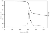
- FIG. 1 is a diagram showing the results of thermogravimetric analysis of the semiconductor nanoparticle composite according to the embodiment of the present invention.
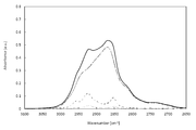
- FIG. 2 is a diagram showing infrared absorption spectra of the semiconductor nanoparticle composite and the ligand alone according to the embodiment of the present invention.
- FIG. 3 is a diagram in which actually measured values and calculated values of the infrared absorption spectrum of the semiconductor nanoparticle composite according to the embodiment of the present invention are fitted.
- FIG. 4 is a diagram showing the composition of the infrared absorption spectrum of each ligand component in the fitting curve for the absorption peak of CH expansion and contraction of the semiconductor nanoparticle composite according to the embodiment of the present invention.
- FIG. 1 is a diagram showing the results of thermogravimetric analysis of the semiconductor nanoparticle composite according to the embodiment of the present invention.
- FIG. 2 is a diagram showing infrared absorption spectra of the semiconductor nanoparticle composite and the ligand alone according to the embodiment of the present invention.
- FIG. 3
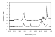
- FIG. 5 is a diagram showing infrared absorption spectra of the semiconductor nanoparticle composite according to the embodiment of the present invention before and after the heat treatment.
- FIG. 6 is a diagram showing the results of thermogravimetric analysis of the semiconductor nanoparticle composite of Example 10.
- FIG. 7 is a diagram showing the results of thermogravimetric analysis of the semiconductor nanoparticle composite of Example 16.
- FIG. 8 is a diagram showing the results of thermogravimetric analysis of the semiconductor nanoparticle composite of Example 17.
- the present invention relates to a semiconductor nanoparticle composite.
- the semiconductor nanoparticle composite is a semiconductor nanoparticle composite having light emitting characteristics.
- the semiconductor nanoparticle composite of the present invention is a particle that absorbs light of 340 nm to 480 nm and emits light having an emission peak wavelength of 400 nm to 750 nm.
- the full width at half maximum (FWHM) of the emission spectrum of the semiconductor nanoparticle composite is preferably 40 nm or less, and more preferably 38 nm or less.
- FWHM full width at half maximum
- the fluorescence quantum efficiency (QY) of the semiconductor nanoparticle composite is preferably 80% or more, and more preferably 85% or more.
- QY fluorescence quantum efficiency
- the fluorescence quantum efficiency of the semiconductor nanoparticle composite can be measured using a quantum efficiency measuring system.
- the semiconductor nanoparticles constituting the semiconductor nanoparticles composite are not particularly limited as long as they satisfy the above-mentioned fluorescence quantum efficiency and light emission characteristics such as half-price width, and may be particles made of one type of semiconductor. It may be a particle composed of two or more different semiconductors. In the case of particles composed of two or more different semiconductors, the core-shell structure may be composed of those semiconductors.
- the type of semiconductor is not particularly limited, and examples thereof include InP, GaP, CdSe, CdS, ZnS, ZnSe, and ZnS. In particular, a non-Cd semiconductor is preferable.
- the semiconductor nanoparticles may contain a composition other than the semiconductor as long as the characteristics of the semiconductor nanoparticles are not impaired.
- a core-shell type having a core containing a group III element and a group V element and a shell containing a group II element and a group VI element covering at least a part of the core. It may be a particle.
- the shell may have a plurality of shells having different compositions, or may have one or more gradient-type shells in which the ratio of the elements constituting the shell changes in the shell.
- Group III element examples include In, Al and Ga.
- Group V element examples include P, N and As.
- the composition for forming the core is not particularly limited, but InP is preferable from the viewpoint of light emission characteristics.
- the group II element is not particularly limited, and examples thereof include Zn and Mg.
- Group VI elements include, for example, S, Se, Te, and O.
- the composition for forming the shell is not particularly limited, but from the viewpoint of the quantum confinement effect, ZnS, ZnSe, ZnSeS, ZnTeS, ZnTeSe and the like are preferable. In particular, when the Zn element is present on the surface of the semiconductor nanoparticles, the effect of the present invention can be more exerted.
- At least one shell having the above-mentioned composition may be included.
- the shell has a gradient type shell in which the ratio of the elements constituting the shell changes, the shell does not necessarily have to have the composition according to the composition notation.
- whether or not the shell covers at least a part of the core and the element distribution inside the shell use, for example, energy dispersive X-ray spectroscopy (TEM-EDX) using a transmission electron microscope. It can be confirmed by composition analysis and analysis.
- TEM-EDX energy dispersive X-ray spectroscopy
- a core of semiconductor nanoparticles can be formed by mixing a group III precursor, a group V precursor, and an additive if necessary in a solvent, and heating the obtained precursor mixture. ..
- a coordinating solvent or a non-coordinating solvent is used as the solvent. Examples of solvents include 1-octadecene, hexadecane, squalene, oleylamine, trioctylphosphine, trioctylphosphine oxide and the like.
- Examples of the Group III precursor include, but are not limited to, acetates, carboxylates, halides and the like containing the Group III elements.
- Examples of the Group V precursor include, but are not limited to, the organic compounds and gases containing the Group V elements.
- the precursor is a gas
- a core can be formed by reacting while injecting a gas into a precursor mixture containing a mixture other than the gas.
- the semiconductor nanoparticles may contain one or more elements other than group III and group V as long as the effects of the present invention are not impaired.
- a precursor of the elements may be added at the time of core formation.
- the additive include, but are not limited to, carboxylic acids, amines, thiols, phosphines, phosphine oxides, phosphinic acids, and phosphonic acids as dispersants.
- the dispersant can also serve as a solvent.
- a halide is added to improve the light emitting characteristics of the semiconductor nanoparticles.
- the In precursor and, if necessary, a metal precursor solution with a dispersant added to the solvent are mixed under vacuum, once heated at 100 ° C. to 300 ° C. for 6 to 24 hours, and then further.
- the P precursor is added and heated at 200 ° C. to 400 ° C. for 3 to 60 minutes and then cooled.
- a halogen precursor and heat-treating at 25 ° C. to 300 ° C., preferably 100 ° C. to 300 ° C., more preferably 150 ° C. to 280 ° C., a core particle dispersion containing core particles can be obtained. ..
- the semiconductor nanoparticles By adding the shell-forming precursor to the synthesized core particle dispersion, the semiconductor nanoparticles have a core-shell structure, and the fluorescence quantum efficiency (QY) and stability can be improved.
- the elements that make up the shell are thought to have a structure such as an alloy, heterostructure, or amorphous structure on the surface of the core particles, but it is also possible that some of them have moved to the inside of the core particles due to diffusion.
- the added shell-forming element mainly exists near the surface of the core particles and has a role of protecting the semiconductor nanoparticles from external factors.
- the shell covers at least a part of the core, and more preferably the entire surface of the core particles is uniformly covered.
- the Zn precursor and the Se precursor are added to the above-mentioned core particle dispersion and then heated at 150 ° C. to 300 ° C., preferably 180 ° C. to 250 ° C., and then the Zn precursor and the S precursor are added. , 200 ° C. to 400 ° C., preferably 250 ° C. to 350 ° C.
- the Zn precursor includes carboxylates such as zinc acetate, zinc propionate and zinc myristate, halides such as zinc chloride and zinc bromide, and organic substances such as diethylzinc. Salt or the like can be used.
- phosphine serenides such as tributylphosphine serenide, trioctylphosphine serenide and tris (trimethylsilyl) phosphine serenide, selenols such as benzenelenol and selenocysteine, and a selenium / octadecene solution are used. can do.
- phosphine sulfides such as tributylphosphine sulfide, trioctylphosphine sulfide and tris (trimethylsilyl) phosphine sulfide, thiols such as octanethiol, dodecanethiol and octadecanethiol, and sulfur / octadecene solutions should be used.
- the shell precursors may be premixed and added once or in multiple doses, or separately, once or in multiple doses. When the shell precursor is added in a plurality of times, the temperature may be changed and heated after each shell precursor is added.
- the method for producing semiconductor nanoparticles is not particularly limited, and in addition to the methods shown above, conventional methods such as a hot injection method, a uniform solvent method, a reverse micelle method, and a CVD method can be used. , Any method may be adopted.
- the semiconductor nanoparticle composite is one in which a ligand is coordinated on the surface of the semiconductor nanoparticles.
- the coordination described here means that the ligand chemically affects the surface of the semiconductor nanoparticles. It may be coordinated to the surface of the semiconductor nanoparticles or in any other bonding mode (eg, covalent bond, ionic bond, hydrogen bond, etc.) or coordinated to at least a portion of the surface of the semiconductor nanoparticles. If it has children, it does not necessarily have to form a bond.
- the ligand that coordinates the semiconductor nanoparticles consists of an organic group and a coordinating group.
- the ligand in the semiconductor nanoparticle composite of the present invention includes an aliphatic ligand in which the organic group is an aliphatic hydrocarbon group and a polar ligand in which the organic group contains a hydrophilic functional group.
- the aliphatic ligand preferably has one coordinating group and at least one or more aliphatic hydrocarbon groups bonded thereto.
- the coordinating group of the aliphatic ligand is preferably selected from the group consisting of an amino group, a carboxyl group, a mercapto group, a phosphine group, and a phosphine oxide group.
- the polar ligand has a hydrophilic functional group as an organic group.
- the organic group of the polar ligand may have at least one of a hydroxyl group, a carboxyl group, a carbonyl group, a mercapto group, an amino group, an ether bond, an ester bond, and a siloxane bond as a hydrophilic functional group.
- Having a hydrophilic functional group in the organic group of the polar ligand enables dispersion in a polar dispersion medium.
- the polar ligand when the coordinating group of the polar ligand is a mercapto group, the polar ligand can strongly coordinate with the semiconductor nanoparticles, so that high fluorescence quantum efficiency can be obtained and the heat resistance of the semiconductor nanoparticles composite can be improved.
- the molecular weight of the polar ligand is preferably 50 or more and 600 or less, and more preferably 50 or more and 450 or less.
- a ligand having a molecular weight of 600 or less it is possible to suppress an increase in the size and volume of the semiconductor nanoparticle composite, and when applying the semiconductor nanoparticle composite to a dispersion liquid, a composition, a cured film, etc. It becomes easy to increase the mass fraction of the semiconductor nanoparticle composite with respect to these.
- the molecular weight is 50 or more, the effect of steric hindrance is sufficiently exhibited, and when the semiconductor nanoparticle composite is dispersed in the dispersion medium, the occurrence of aggregation and the like can be suppressed.
- the mass ratio (aliphatic ligand / polar ligand) of the aliphatic ligand and the polar ligand is preferably 0.05 to 1.00, more preferably 0.10 to 1.00, and 0.20 to 0.20 to 1.00. It is still more preferably 0.80.
- the semiconductor nanoparticle composite can be dispersed in a dispersion medium having a high SP value, and a semiconductor nanoparticle composite having high heat resistance can be obtained.
- the mass ratio of the ligand to the semiconductor nanoparticles is preferably 0.1 to 0.7.
- the mass ratio of the ligand to the semiconductor nanoparticles is in this range, it is possible to suppress an increase in the size and volume of the semiconductor nanoparticles composite, and to use the semiconductor nanoparticles composite in a dispersion liquid, a composition, a cured film, or the like. When applied, the mass ratio of the semiconductor nanoparticle composite to these can be increased.
- the mass ratio of the ligand to the semiconductor nanoparticles (ligand / semiconductor nanoparticles) is more preferably 0.1 to 0.5.
- the method of coordinating the ligand to the semiconductor nanoparticles is not limited, but a ligand exchange method utilizing the coordinating force of the ligand can be used.
- the semiconductor nanoparticles in which the organic compound used in the process of producing the semiconductor nanoparticles described above is coordinated with the surface of the semiconductor nanoparticles are brought into contact with the target ligand in a liquid phase.
- a semiconductor nanoparticle complex in which the target ligand is coordinated on the surface of the semiconductor nanoparticles can be obtained.
- a liquid phase reaction using a solvent as described later is usually carried out, but when the ligand to be used is a liquid under the reaction conditions, the ligand itself is used as a solvent and another solvent is not added. Is also possible.
- the desired ligand can be easily coordinated.
- a non-coordinating solvent is used in the synthesis of the semiconductor nanoparticles, the formation of surface defects of the semiconductor nanoparticles can be minimized when the desired ligand is coordinated, and the fluorescence quantum efficiency is lowered. Can be prevented.
- the semiconductor nanoparticle-containing dispersion after the semiconductor nanoparticles are produced is purified, redispersed, and then a solvent containing an aliphatic ligand is added, and a solvent containing a polar ligand is further added under a nitrogen atmosphere.
- the desired semiconductor nanoparticle composite can be obtained by stirring at 50 ° C. to 200 ° C. for 1 minute to 120 minutes.
- the aliphatic ligand and the polar ligand may be added at the same time.
- the semiconductor nanoparticles and the semiconductor nanoparticle composite can be purified as follows.
- the semiconductor nanoparticle composite can be precipitated from the dispersion by adding a polarity conversion solvent such as acetone.
- the precipitated semiconductor nanoparticle composite can be recovered by filtration or centrifugation, while the supernatant containing unreacted starting material and other impurities can be discarded or reused.
- the precipitated semiconductor nanoparticle composite can then be washed with a further dispersion medium and dispersed again. This purification process can be repeated, for example, 2-4 times, or until the desired purity is reached.
- the method for purifying the semiconductor nanoparticle composite is not particularly limited, and in addition to the methods shown above, for example, aggregation, liquid-liquid extraction, distillation, electrodeposition, size exclusion chromatography and / or ultrafiltration, etc. Any method can be used alone or in combination.
- the state in which the semiconductor nanoparticle composite is dispersed in the dispersion medium means that the semiconductor nanoparticle composite does not precipitate when the semiconductor nanoparticle composite and the dispersion medium are mixed, or is visually turbid. Indicates that the state does not remain as (cloudy).
- a semiconductor nanoparticle composite dispersed in a dispersion medium is referred to as a semiconductor nanoparticle composite dispersion liquid.
- the semiconductor nanoparticle composite of the present invention can be dispersed in a dispersion medium to form a semiconductor nanoparticle composite dispersion liquid. It is preferable that the semiconductor nanoparticle composite can be dispersed in the dispersion medium to form a dispersion liquid even if the SP value of the dispersion medium is 9.0 or more.
- the SP value here is a Hildebrand solubility parameter, which is a value calculated from the Hansen solubility parameter.
- the Hansen solubility parameter is described in the handbook, eg, "Hansen Solubility Parameters: A User's Handbook", 2nd Edition, C.I. M. The values in Hanson (2007), Hanson and Abbot et al. It can be determined using the Practice (HSPiP) program (2nd edition) provided by.
- PMEA propylene glycol monomethyl ether acetate
- PGME propylene glycol monomethyl ether
- IPA ethanol
- methanol methanol
- PGMEA is generally used as a diluting solvent, and if the semiconductor nanoparticle composite can be dispersed in PGMEA, the semiconductor nanoparticle composite can be widely applied in the photoresist field. ..
- a monomer can be selected as a dispersion medium for dispersing the semiconductor nanoparticle composite.
- the monomer is not particularly limited, but an acrylic monomer that can be widely selected for application of semiconductor nanoparticles is preferable.
- the (meth) acrylic monomer is methyl (meth) acrylate, ethyl (meth) acrylate, propyl (meth) acrylate, butyl (meth) acrylate, isobutyl (meth) acrylate, isoamyl, depending on the application of the semiconductor nanoparticle composite dispersion.
- the acrylic monomer may be one or a mixture of two or more selected from lauryl (meth) acrylate and 1,6-hexadioldi (meth) acrylate depending on the application of the semiconductor nanoparticle composite dispersion. preferable.
- the semiconductor nanoparticle composite can be dispersed in the dispersion medium at a high mass fraction.
- the semiconductor nanoparticle composite is preferably dispersible in at least one of the dispersion medium and the monomer so that the mass fraction of the semiconductor nanoparticles is 25% by mass or more.
- FIG. 1 shows the results of thermal analysis of the semiconductor nanoparticle composite of an embodiment of the present invention.
- Thermal analysis is performed by thermogravimetric analysis and ligand identification.
- the thermogravimetric analysis is performed by heating the semiconductor nanoparticle composite to 550 ° C. at 10 ° C./min under a nitrogen atmosphere using differential thermal weight analysis (DTA-TG), holding it for 10 minutes, and lowering the temperature. It was.
- the solid line is the result of thermogravimetric analysis (TG), and the broken line is the result of the derivative of TG ( ⁇ TG).
- TG thermogravimetric analysis
- ⁇ TG derivative of TG
- the ligand in the semiconductor nanoparticle composite is almost desorbed by 500 ° C.
- the ratio of the amount of ligand to the total semiconductor nanoparticles in the form was calculated to be 32%.
- the mass reduction rate ( XH ) of the semiconductor nanoparticle composite of the present embodiment was 6% in the range of 350 ° C. or higher and 550 ° C. or lower.
- the semiconductor nanoparticle composite according to the embodiment of the present invention has a mass fraction (L) of all ligands with respect to the semiconductor nanoparticle composite at room temperature in a range of 350 ° C. or higher and 550 ° C. or lower in thermal weight analysis.
- the ratio of the mass reduction rate ( XH ) of the semiconductor nanoparticle composite ( ⁇ ( XH ) / L ⁇ ⁇ 100) is 10 or more and 55 or less. This means that of all the ligands coordinated to the semiconductor nanoparticles at room temperature, the ligands of 10 to 55 by mass are not in the low temperature range of room temperature to 350 ° C, but 350 ° C or higher and 550.
- the semiconductor nanoparticles are separated from the surface in the high temperature range of °C or less.
- the proportion of the ligand that leaves the surface of the semiconductor nanoparticles in the high temperature range of 350 ° C. or higher and 550 ° C. or lower is 10 to 55, it becomes an index for obtaining a semiconductor nanoparticle composite having high optical characteristics.
- the above ratio ( ⁇ (X H ) / L ⁇ ⁇ 100) is more preferably 10 to 50.
- the semiconductor nanoparticle composite according to another embodiment of the present invention has a mass reduction rate of the semiconductor nanoparticle composite in the range of 350 ° C. or higher and 550 ° C. or lower (semiconductor in the range of (350 ° C. to 550 ° C.).
- (Mass reduction amount of nanoparticle composite) / (mass of semiconductor nanoparticle composite at room temperature) ⁇ 100) is 2% or more and 15% or less.
- the semiconductor nanoparticle composite has high fluorescence quantum efficiency.
- the semiconductor nanoparticle composite according to an embodiment of the present invention has a “mass reduction in the range of room temperature to 350 ° C.” with respect to “mass fraction reduction (X) when the semiconductor nanoparticle composite is heated from room temperature to 700 ° C.”. rate as the ratio of (X L) "(X L / X),” polar ligand to semiconductor nanoparticles complex at "room temperature to the total mass fraction of the ligand (L)” with respect to the semiconductor nanoparticle complex at room temperature relationship between the ratio of the mass fraction (L P) "is preferably a (X L / X) ⁇ ( L P / L).
- the absorption peaks appearing in 2300 cm -1 to 2500 cm -1 are due to carbon dioxide.
- FIGS. 2 (b), 2 (c), and 2 (d) show infrared absorption spectra of the ligand alone, which is considered to be present in the semiconductor nanoparticle composite of the present embodiment.
- one polar ligand and two aliphatic ligands are coordinated to the semiconductor nanoparticles.
- the ligand (b) is a polar ligand
- the ligand (c) and the ligand (d) are aliphatic ligands. Since the absorbance of the infrared absorption spectrum is proportional only to the concentration and thickness of the substance, it is possible to perform quantitative analysis from the peak area.
- the infrared absorption spectrum of the semiconductor nanoparticle conjugate S QD ( ⁇ ), the infrared absorption spectrum of the i-th aliphatic ligand S ai ( ⁇ ), the infrared absorption spectrum of the i-th polar ligand S pi ( ⁇ ) is expressed as the equation (1).
- S QD ( ⁇ ) ⁇ aiS ai ( ⁇ ) + ⁇ piS pi ( ⁇ ) Equation (1)
- ⁇ is a wave number
- ai and pi are constants related to the mole fraction of the aliphatic ligand and the polar ligand, respectively.
- the spectrum of the polar ligand of (b) is S (b) ( ⁇ )
- the spectra of the aliphatic ligands of (c) and (d) are S, respectively. If (c) ( ⁇ ) and S (d) ( ⁇ ), it is expressed as in the equation (2).
- S QD ( ⁇ ) bS (b) ( ⁇ ) + cS (c) ( ⁇ ) + dS (d) ( ⁇ ) Equation (2)
- ⁇ is a wave number
- b, c, and d are constants.
- FIG. 3 is a fitting of the measured value and the calculated value of the infrared absorption spectrum.
- the dotted line is the measured value and the solid line is the calculated value. It can be seen that the calculated values often represent the measured values.
- FIG. 4 shows the composition of the infrared absorption spectrum of each ligand component in the fitting curve of the absorption peak of CH expansion and contraction.
- the dotted line shows the measured infrared absorption spectrum of the semiconductor nanoparticle composite
- the gray solid line shows the measured infrared absorption spectrum of the ligand (b).
- the gray broken lines in are shown by the measured infrared absorption spectra of the ligands (c) and (d), respectively. It can be seen that the solid black line is the calculated value, and the calculated value often represents the measured value.
- the composition of the ligand can be obtained from the peak area ratio of each ligand component obtained by waveform separation.
- the mass fraction of each ligand component was calculated from the peak area ratio, the number of protons in the molecule, and the molecular weight.
- FIG. 4 shows the measurement results of the semiconductor nanoparticle complex obtained in Example 1 described later.
- FIG. 5 shows an infrared absorption spectrum of the semiconductor nanoparticle composite of the present embodiment before and after the heat treatment.
- the solid line is the infrared absorption spectrum of the semiconductor nanoparticle composite before heat treatment
- the broken line is the infrared absorption spectrum of the semiconductor nanoparticle composite heated to 350 ° C. at 10 ° C./min in a nitrogen atmosphere and cooled to room temperature.
- a sharp absorption peak of CO expansion and contraction is observed around 1100 cm -1 , while this peak intensity is considerably high in the semiconductor nanoparticle composite heated to 350 ° C.
- the method for calculating the mass fraction (L) of all ligands with respect to the semiconductor nanoparticle composite at room temperature is as follows.
- the end point is the point where the mass reduction amount of the semiconductor nanoparticle composite is almost constant
- the mass reduction amount up to the end point indicates the total amount of ligands coordinated to the semiconductor nanoparticles at room temperature.
- the desorption temperature of the ligand changes depending on the type of ligand coordinated to the semiconductor nanoparticles. Therefore, in order to calculate the mass fraction (L) of all ligands with respect to the semiconductor nanoparticle composite at room temperature, the thermogravimetric analysis result (mass reduction amount) when the heating temperature is 700 ° C. or higher is used. You just have to judge.
- thermoweight analysis and infrared absorption spectrum Based on the above measurement results of thermoweight analysis and infrared absorption spectrum, it is said that when the semiconductor nanoparticle composite described in the present application is heated, the aliphatic ligand is desorbed from the surface of the semiconductor nanoparticles at a temperature higher than that of the polar ligand. It turns out that there is a feature. Furthermore, at least a part of the components desorbed at 350 ° C. or higher is attributed to the aliphatic ligand. As a reference, it is disclosed that the aliphatic ligand (dodecanethiol) described in Non-Patent Document 6 is eliminated from the bound Zn at about 250 ° C. to 300 ° C.
- the desorption temperature of the aliphatic ligand in the semiconductor nanoparticle complex described in the present application is higher than that in the literature.
- the desorption temperature of the ligand is greatly affected not only by the chemical structure but also by the interaction with surrounding atoms and molecules, such as the coordination form with Zn existing on the surface of the semiconductor nanoparticles and the formation of the crystal structure of the ligand. It is conceivable that the aliphatic ligand coordinated to the semiconductor nanoparticles described in the present application is strongly bound on the surface of the semiconductor nanoparticles due to the factors as described above, and exhibits a high desorption temperature.
- the inventors speculate that the presence of such a strongly bound aliphatic ligand on the surface of the semiconductor nanoparticles improves the fluorescence quantum efficiency of the semiconductor nanoparticles.
- the inventors speculate that the presence of the above-mentioned aliphatic ligand also has the effect of improving heat resistance.
- the semiconductor nanoparticle composite of the present invention adopts the following constitution.
- a semiconductor nanoparticle complex in which two or more ligands including an aliphatic ligand and a polar ligand are coordinated on the surface of semiconductor nanoparticles.
- the ligand consists of an organic group and a coordinating group.
- the organic group is an aliphatic hydrocarbon group.
- the polar ligand contains a hydrophilic functional group in the organic group.
- the mass ratio of the aliphatic ligand to the polar ligand (aliphatic ligand / polar ligand) is 0.05 to 1.00.
- Mass fraction (X H ) of the semiconductor nanoparticle composite in the range of 350 ° C.
- the ligand consists of an organic group and a coordinating group. In the aliphatic ligand, the organic group is an aliphatic hydrocarbon group.
- the polar ligand contains a hydrophilic functional group in the organic group.
- the mass ratio of the aliphatic ligand to the polar ligand is 0.05 to 1.00.
- the mass reduction rate ( XH ) of the semiconductor nanoparticle composite in the range of 350 ° C. or higher and 550 ° C. or lower is 2% or more and 15% or less.
- thermogravimetric analysis The ratio ( XL / X) of the mass loss rate ( XL ) in the range of room temperature to 350 ° C. to the mass loss rate (X) when the semiconductor nanoparticle composite is heated from room temperature to 700 ° C.
- Mass fraction of total ligand to semiconductor nanoparticles complex at room temperature for (L) the mass fraction of polar ligand to semiconductor nanoparticles complex at room temperature with (L P) ratio (L P / L), the Relationship, (X L / X) is ⁇ (L P / L),
- the semiconductor nanoparticle composite according to any one of (1) to (3) above.
- the semiconductor nanoparticle composite can be dispersed in a dispersion medium having an SP value of 9.0 to 15.0.
- the dispersion medium is one or more mixed dispersion media selected from the group consisting of acetone, PGMEA, PGME, IPA, ethanol, and methanol.
- At least a part of the mass loss at 350 ° C. or higher is attributed to the elimination of the aliphatic ligand.
- the aliphatic ligand has one coordinating group and at least one or more aliphatic hydrocarbon groups bonded thereto.
- the molecular weight of the polar ligand is 50 or more and 600 or less.
- the molecular weight of the polar ligand is 50 or more and 450 or less.
- the coordinating group of the aliphatic ligand is selected from the group consisting of an amino group, a carboxyl group, a mercapto group, a phosphine group, and a phosphine oxide group.
- the organic group of the polar ligand has at least one of a hydroxyl group, a carboxyl group, a carbonyl group, a mercapto group, an amino group, an ether bond, an ester bond, and a siloxane bond.
- the coordinating group of the polar ligand is a mercapto group.
- the mass ratio of the ligand to the semiconductor nanoparticles (ligand / semiconductor nanoparticles) is 0.1 to 0.7.
- the mass ratio of the ligand to the semiconductor nanoparticles is 0.1 to 0.5.
- the semiconductor nanoparticles can be dispersed in the dispersion medium so as to have a mass fraction of 25% by mass or more.
- the semiconductor nanoparticles can be dispersed in the dispersion medium so as to have a mass fraction of 35% by mass or more.
- the semiconductor nanoparticles contain Zn on the surface of the semiconductor nanoparticles.
- the reaction mixture was cooled to 25 ° C., octanoic acid chloride (0.45 mmol) was injected, heated at about 250 ° C. for 30 minutes, and then cooled to 25 ° C. Then, the mixture was heated to 200 ° C., 0.75 mL of a Zn precursor solution and 0.3 mmol of selenate trioctylphosphine were simultaneously added, and the mixture was reacted for 30 minutes to form a ZnSe shell on the surface of InP-based semiconductor nanoparticles. Further, 1.5 mL of a Zn precursor solution and 0.6 mmol of trioctylphosphine sulfide were added, and the temperature was raised to 250 ° C.
- the reaction solution of the semiconductor nanoparticles obtained by the synthesis as described above was added to acetone, mixed well, and then centrifuged. The centrifugal acceleration was 4000 G. The precipitate was recovered, and normal hexane was added to the precipitate to prepare a dispersion. This operation was repeated several times to obtain purified semiconductor nanoparticles.
- the semiconductor nanoparticle composite was synthesized according to the following method.
- (Making a single ligand) ⁇ Preparation of PEG-SH>
- the flask contained 210 g of methoxyPEG-OH (molecular weight 400) and 93 g of triethylamine and was dissolved in 420 mL of THF (tetrahydrofuran).
- THF tetrahydrofuran
- the solution was cooled to 0 ° C., and 51 g of methanesulfonic acid chloride was gradually added dropwise under a nitrogen atmosphere, taking care that the temperature of the reaction solution did not exceed 5 ° C. due to the heat of reaction. Then, the reaction solution was heated to room temperature and stirred for 2 hours.
- This solution was extracted with a chloroform-aqueous system to recover the organic phase.
- PEG having a molecular weight of 400 is used in the same manner except that PEG-SH methoxyPEG-OH (molecular weight 400, 210 g) is changed to methoxy PEG-OH (molecular weight 600, 315 g). -SH was obtained.
- the reaction solution was filtered and the filtrate was diluted with chloroform.
- the solution was extracted in the order of 10% HCl aqueous solution, 10% Na 2 CO 3 aqueous solution, and saturated NaCl aqueous solution, and the organic phase was recovered.
- the organic phase was concentrated by evaporation and then purified by column chromatography using a hexane-ethyl acetate mixed solvent as a developing solvent to obtain the desired product.
- a semiconductor nanoparticle 1-octadecene dispersion was prepared by dispersing the purified semiconductor nanoparticles in a flask with 1-octadecene so as to have a mass ratio of 10% by mass. 10.0 g of the prepared semiconductor nanoparticles 1-octadecene dispersion was placed in a flask, 0.2 g of dodecanethiol (DDT) was added as an aliphatic ligand, 4.0 g of PEG-SH was added as a polar ligand, and nitrogen was added. The semiconductor nanoparticle composite was obtained by stirring at 110 ° C. for 60 minutes in an atmosphere and cooling to 25 ° C.
- DDT dodecanethiol
- the reaction solution containing the semiconductor nanoparticle composite was transferred to a centrifuge tube and centrifuged at 4000 G for 20 minutes to separate into a transparent 1-octadecene phase and a semiconductor nanoparticle composite phase.
- the 1-octadecene phase was removed and the remaining semiconductor nanoparticle composite phase was recovered.
- the obtained semiconductor nanoparticle composite is dispersed in a dispersion medium, and a single light of 450 nm is applied to obtain an emission spectrum.
- the fluorescence quantum efficiency (QY) and the half-value width (FWHM) were calculated from the emission spectrum after re-excitation correction excluding the re-excitation fluorescence emission spectrum of the portion that was re-excited and fluorescently emitted from the emission spectrum obtained here.
- PGMEA was used as the dispersion. If it did not disperse in PGMEA, the dispersion was changed to normal hexane.
- FIG. 1 shows a TG curve and its derivative ( ⁇ TG) curve when the semiconductor nanoparticle composite (Example 1) having the above-described configuration is heated from 25 ° C. to 550 ° C. at 10 ° C./min by thermogravimetric analysis (TGA). Shown. The measurement was performed using a Bruker TG-DTA2000SA under a nitrogen flow of 200 ml / min. In the semiconductor nanoparticle composite of Example 1, the mass reduction rate in the range from room temperature to 350 ° C. is 25%, and the mass reduction rate of the semiconductor nanoparticle composite in the range of 350 ° C. or higher and 550 ° C. or lower is 7. %Met. Furthermore, from the ⁇ TG curve, two peaks were confirmed at around 310 ° C and around 430 ° C.
- the total mass reduction rate when the semiconductor nanoparticle composite is heated to 700 ° C. is regarded as the mass fraction (L) of all ligands with respect to the semiconductor nanoparticle composite at room temperature. Further, in the thermogravimetric analysis, the semiconductor nanoparticle composite was heated to 700 ° C., and the residual mass after the measurement was taken as the mass of the semiconductor nanoparticles. From this value, the mass fraction (Q) of the semiconductor nanoparticles with respect to the semiconductor nanoparticles composite at room temperature was confirmed.
- Example 2 In the step of producing the semiconductor nanoparticle composite, the semiconductor nanoparticle composite was prepared in the same manner as in Example 1 except that 0.5 g of dodecanethiol was used as the aliphatic thiol ligand and 4.0 g of PEG-SH was used as the polar ligand. Obtained.
- Example 3 In the process of preparing the semiconductor nanoparticle complex, 1.0 g of dodecanethiol as an aliphatic thiol ligand and 1.5 g of N-acetyl-N- (2-mercaptoethyl) propanamide as a polar ligand were used, and oleic acid was further added. A semiconductor nanoparticle composite was obtained in the same manner as in Example 1 except that 0.5 g was added.
- Example 4 In the step of preparing the semiconductor nanoparticle complex, 0.5 g of dodecanethiol as an aliphatic thiol ligand, 4.0 g of triethylene glycol monomethyl ether thiol (TEG-SH) as a polar ligand was used, and oleic acid was further added to 0. A semiconductor nanoparticle composite was obtained in the same manner as in Example 1 except that 5 g was added.
- TAG-SH triethylene glycol monomethyl ether thiol
- Example 5 Example 1 except that 0.5 g of octanethiol was used as the aliphatic thiol ligand and 4.0 g of N-acetyl-N- (2-mercaptoethyl) propanamide was used as the polar ligand in the step of preparing the semiconductor nanoparticle complex.
- a semiconductor nanoparticle composite was obtained in the same manner as in.
- Example 6 In the step of producing the semiconductor nanoparticle composite, the semiconductor nano was formed in the same manner as in Example 1 except that 0.5 g of dodecanethiol was used as the aliphatic thiol ligand and 6.0 g of PEG-SH (molecular weight 600) was used as the polar ligand. A particle complex was obtained.
- Example 7 In the step of preparing a shell of semiconductor nanoparticles, a mixture of 40 mmol of zinc octanate and 75 mL of octadecene was used as the Zn precursor solution. Further, in the step of preparing the semiconductor nanoparticle complex, 0.5 g of dodecanethiol as an aliphatic thiol ligand and 4.0 g of N-acetyl-N- (2-mercaptoethyl) propanamide as a polar ligand were used. A semiconductor nanoparticle composite was obtained in the same manner as in Example 1 except that 0.5 g of caprylic acid (octanoic acid) was added.
- caprylic acid octanoic acid
- Example 8 Same as Example 1 except that 0.5 g of dodecanethiol was used as the aliphatic thiol ligand and 4.0 g of methyl 3-mercaptopropionate (manufactured by Tokyo Kasei Kogyo Co., Ltd.) was used as the polar ligand in the process of producing the semiconductor nanoparticle complex.
- a semiconductor nanoparticle composite was obtained by the above method.
- Example 9 In the step of producing the semiconductor nanoparticle composite, the semiconductor nanoparticle composite was prepared in the same manner as in Example 1 except that 0.2 g of dodecanethiol was used as the aliphatic thiol ligand and 8.0 g of PEG-SH was used as the polar ligand. Obtained.
- Example 10 Example 1 except that 0.5 g of cyclopentanethiol as an aliphatic thiol ligand, 4.0 g of PEG-SH as a polar ligand, and 0.5 g of oleic acid were added in the step of preparing the semiconductor nanoparticle composite. A semiconductor nanoparticle composite was obtained in the same manner as in.
- FIG. 6 is a graph showing the results of thermal analysis of the semiconductor nanoparticle composite of Example 10.
- the solid line is the TG curve, and the broken line is the ⁇ TG curve.
- cyclopentanethiol is used as the aliphatic ligand and PEG-SH is used as the polar ligand.
- PEG-SH is used as the polar ligand.
- a peak due to desorption of cyclopentanethiol was observed near 230 ° C. and a peak due to PEG-SH was observed near 310 ° C., respectively.
- the fluorescence quantum efficiency of the semiconductor nanoparticles is low.
- Example 11 Example 1 except that 0.5 g of pentane thiol was used as an aliphatic thiol ligand, 4.0 g of PEG-SH was used as a polar ligand, and 0.5 g of oleic acid was further added in the step of preparing the semiconductor nanoparticle composite. A semiconductor nanoparticle composite was obtained in the same manner.
- Example 12 In the step of making a shell of semiconductor nanoparticles, a mixture of 40 mmol zinc acetate and 75 mL octadecene was used as the Zn precursor solution. Further, in the step of preparing the semiconductor nanoparticle complex, Example 1 except that 0.5 g of dodecanethiol was used as an aliphatic thiol ligand, 4.0 g of PEG-SH was used as a polar ligand, and 0.5 g of acetic acid was further added. A semiconductor nanoparticle composite was obtained in the same manner as in.
- Example 13 In the step of preparing the semiconductor nanoparticle composite, 2.0 g of an aliphatic thiol ligand was added, the polar ligand was changed to PEG-SH, and 1.0 g of oleic acid was further added. The mixture was stirred at 110 ° C. for 60 minutes under a nitrogen atmosphere and cooled to 25 ° C. 5.0 mL of normal hexane was added to the reaction solution to prepare a dispersion. 50 mL of ethanol was added to the obtained dispersion, and the mixture was centrifuged at 4000 G for 20 minutes. After centrifugation, the clear supernatant was removed and the precipitate was collected. This operation was repeated several times to obtain a purified semiconductor nanoparticle composite.
- Example 14 In the step of producing the semiconductor nanoparticle composite, the semiconductor nano was formed in the same manner as in Example 1 except that 0.5 g of dodecanethiol was used as the aliphatic thiol ligand and 7.5 g of PEG-SH (molecular weight 750) was used as the polar ligand. A particle complex was obtained.
- Example 15 In the step of producing the semiconductor nanoparticle composite, the semiconductor nano was formed in the same manner as in Example 1 except that 0.5 g of dodecanethiol was used as the aliphatic thiol ligand and 10.0 g of PEG-SH (molecular weight 1000) was used as the polar ligand. A particle complex was obtained.
- Example 16 The flask contained 1.0 g of the semiconductor nanoparticle composite purified in the same manner as in Example 1, 10 mL of isopropanol, and 4.0 g of PEG-SH. The solution was stirred at 80 ° C. for 180 minutes under a nitrogen atmosphere and cooled to 25 ° C. 50 mL of normal hexane was added to the reaction solution, and the mixture was centrifuged at 4000 G for 20 minutes. After centrifugation, the clear supernatant was removed and the precipitate was collected. 5.0 mL of acetone was added to the precipitate to prepare a dispersion.
- FIG. 7 is a graph showing the results of thermal analysis of the semiconductor nanoparticle composite of Example 16.
- the solid line is the TG curve
- the broken line is the ⁇ TG curve.
- ⁇ TG curve of the semiconductor nanoparticle composite of Example 16 a sharp single peak was observed near 300 ° C.
- PEG-SH polar ligand
- the ligand desorbed in the range of 350 ° C. or higher and 550 ° C. or lower was also identified using the infrared absorption spectrum, the ligand desorbed in the range of 350 ° C. or higher and 550 ° C.
- the mass loss rate in the range of 350 ° C. or higher and 550 ° C. or lower was 1%. As described above, when the mass reduction rate in the range of 350 ° C. or higher and 550 ° C. or lower is less than 2%, the fluorescence quantum efficiency of the semiconductor nanoparticle composite becomes low.
- Example 17 Example 1 except that 0.5 g of dodecanethiol as an aliphatic thiol ligand, 2.0 g of PEG-SH as a polar ligand, and 2.0 g of oleic acid were added in the step of preparing the semiconductor nanoparticle composite. A semiconductor nanoparticle composite was obtained in the same manner.
- FIG. 8 is a graph showing the results of thermal analysis of the semiconductor nanoparticle composite of Example 17.
- the solid line is the TG curve, and the broken line is the ⁇ TG curve.
- Dodecanethiol and oleic acid are used as aliphatic ligands, and PEG-SH is used as polar ligands.
- a peak due to desorption of the polar ligand was observed near 310 ° C.
- a peak due to desorption of the aliphatic ligand was observed around 440 ° C.
- Focusing on the mass reduction rate by thermal analysis the mass reduction rate in the range of 350 ° C. or higher and 550 ° C. or lower was 17%. As described above, when the mass reduction rate in the range of 350 ° C. or higher and 550 ° C. or lower is 15% or more, the fluorescence quantum efficiency of the semiconductor nanoparticle composite becomes low.
- Example 18 In the process of preparing the semiconductor nanoparticle complex, 0.5 g of dodecanethiol as an aliphatic thiol ligand and 2.0 g of N-acetyl-N- (2-mercaptoethyl) propanamide as a polar ligand were used, and oleic acid was further added. A semiconductor nanoparticle composite was obtained in the same manner as in Example 1 except that 2.0 g was added.
- Example 19 In the step of producing the semiconductor nanoparticle composite, 4.0 g of dodecanethiol as an aliphatic thiol ligand was used, and the semiconductor nanoparticle composite was obtained in the same manner as in Example 1 except that no polar ligand was added.
- Example 20 In the step of preparing the semiconductor nanoparticle composite, a semiconductor nanoparticle composite was obtained in the same manner as in Example 1 except that 4.0 g of oleic acid was added without adding the aliphatic thiol ligand and the polar ligand.
- Example 21 In the step of producing the semiconductor nanoparticle composite, a semiconductor nanoparticle composite was obtained by the same method as in Example 1 except that 4.0 g of PEG-SH was used as the polar ligand without adding the aliphatic thiol ligand.
- Table 1 shows the constitution of the ligand of the obtained semiconductor nanoparticle composite
- Table 2 shows the emission characteristics and the results of thermal analysis, and the dispersion state in the dispersion medium.
- the semiconductor nanoparticle composite is preferably one that can be dispersed so that the mass fraction of the semiconductor nanoparticles is 25% by mass or more when dispersed in PGMEA.
- the meanings of the abbreviations shown in Table 1 are as follows. DDT: Dodecane Thiol Oct-SH: Octane Thiol OA: Oleic Acid OctA: Octanoic Acid
Landscapes
- Chemical & Material Sciences (AREA)
- Organic Chemistry (AREA)
- Engineering & Computer Science (AREA)
- Materials Engineering (AREA)
- Inorganic Chemistry (AREA)
- Chemical Kinetics & Catalysis (AREA)
- Health & Medical Sciences (AREA)
- Medicinal Chemistry (AREA)
- Polymers & Plastics (AREA)
- Crystallography & Structural Chemistry (AREA)
- Nanotechnology (AREA)
- Physics & Mathematics (AREA)
- Optics & Photonics (AREA)
- Luminescent Compositions (AREA)
- Led Device Packages (AREA)
Priority Applications (4)
| Application Number | Priority Date | Filing Date | Title |
|---|---|---|---|
| KR1020217039055A KR20220015400A (ko) | 2019-05-31 | 2020-05-29 | 반도체 나노입자 복합체 |
| US17/595,924 US20220325174A1 (en) | 2019-05-31 | 2020-05-29 | Semiconductor nanoparticle complex |
| CN202080039962.1A CN113892195A (zh) | 2019-05-31 | 2020-05-29 | 半导体纳米粒子复合体 |
| JP2021521906A JPWO2020241875A1 (ko) | 2019-05-31 | 2020-05-29 |
Applications Claiming Priority (2)
| Application Number | Priority Date | Filing Date | Title |
|---|---|---|---|
| JP2019103247 | 2019-05-31 | ||
| JP2019-103247 | 2019-05-31 |
Publications (1)
| Publication Number | Publication Date |
|---|---|
| WO2020241875A1 true WO2020241875A1 (ja) | 2020-12-03 |
Family
ID=73553216
Family Applications (1)
| Application Number | Title | Priority Date | Filing Date |
|---|---|---|---|
| PCT/JP2020/021467 WO2020241875A1 (ja) | 2019-05-31 | 2020-05-29 | 半導体ナノ粒子複合体 |
Country Status (6)
| Country | Link |
|---|---|
| US (1) | US20220325174A1 (ko) |
| JP (1) | JPWO2020241875A1 (ko) |
| KR (1) | KR20220015400A (ko) |
| CN (1) | CN113892195A (ko) |
| TW (1) | TW202112654A (ko) |
| WO (1) | WO2020241875A1 (ko) |
Citations (6)
| Publication number | Priority date | Publication date | Assignee | Title |
|---|---|---|---|---|
| WO2015156226A1 (ja) * | 2014-04-08 | 2015-10-15 | Nsマテリアルズ株式会社 | 量子ドット及びその製造方法、並びに、前記量子ドットを用いた成形体、シート部材、波長変換部材、発光装置 |
| WO2017038487A1 (ja) * | 2015-08-31 | 2017-03-09 | 富士フイルム株式会社 | 半導体ナノ粒子、分散液、フィルムおよび半導体ナノ粒子の製造方法 |
| WO2017086362A1 (ja) * | 2015-11-20 | 2017-05-26 | Jsr株式会社 | ナノ粒子集合体及びその製造方法、ナノ粒子集合体組成物、波長変換層、並びにリガンド |
| JP2017533875A (ja) * | 2014-08-11 | 2017-11-16 | ヘンケル・アクチェンゲゼルシャフト・ウント・コムパニー・コマンディットゲゼルシャフト・アウフ・アクチェンHenkel AG & Co. KGaA | 反応性コロイド状ナノ結晶及びナノ結晶複合体 |
| WO2017201386A1 (en) * | 2016-05-19 | 2017-11-23 | Nanosys, Inc. | Method to improve the morphology of core/shell quantum dots for highly luminescent nanostructures |
| JP2019073705A (ja) * | 2017-10-17 | 2019-05-16 | エルジー ディスプレイ カンパニー リミテッド | 発光体、発光フィルム、発光ダイオードおよび発光体を含む発光装置 |
Family Cites Families (4)
| Publication number | Priority date | Publication date | Assignee | Title |
|---|---|---|---|---|
| JP5881045B2 (ja) | 2011-10-11 | 2016-03-09 | 国立研究開発法人産業技術総合研究所 | 量子ドット含有チタン化合物及びその製造方法、並びに該量子ドット含有チタン化合物を用いた光電変換素子 |
| JP6448782B2 (ja) * | 2015-05-28 | 2019-01-09 | 富士フイルム株式会社 | 量子ドット含有組成物、波長変換部材、バックライトユニット、および液晶表示装置 |
| US11421151B2 (en) * | 2016-11-25 | 2022-08-23 | Samsung Electronics Co., Ltd. | Light emitting device and display device including quantum dot |
| US10768485B2 (en) * | 2017-07-05 | 2020-09-08 | Nanoco Technologies Ltd. | Quantum dot architectures for color filter applications |
-
2020
- 2020-05-29 US US17/595,924 patent/US20220325174A1/en active Pending
- 2020-05-29 JP JP2021521906A patent/JPWO2020241875A1/ja active Pending
- 2020-05-29 WO PCT/JP2020/021467 patent/WO2020241875A1/ja active Application Filing
- 2020-05-29 TW TW109118003A patent/TW202112654A/zh unknown
- 2020-05-29 KR KR1020217039055A patent/KR20220015400A/ko unknown
- 2020-05-29 CN CN202080039962.1A patent/CN113892195A/zh active Pending
Patent Citations (6)
| Publication number | Priority date | Publication date | Assignee | Title |
|---|---|---|---|---|
| WO2015156226A1 (ja) * | 2014-04-08 | 2015-10-15 | Nsマテリアルズ株式会社 | 量子ドット及びその製造方法、並びに、前記量子ドットを用いた成形体、シート部材、波長変換部材、発光装置 |
| JP2017533875A (ja) * | 2014-08-11 | 2017-11-16 | ヘンケル・アクチェンゲゼルシャフト・ウント・コムパニー・コマンディットゲゼルシャフト・アウフ・アクチェンHenkel AG & Co. KGaA | 反応性コロイド状ナノ結晶及びナノ結晶複合体 |
| WO2017038487A1 (ja) * | 2015-08-31 | 2017-03-09 | 富士フイルム株式会社 | 半導体ナノ粒子、分散液、フィルムおよび半導体ナノ粒子の製造方法 |
| WO2017086362A1 (ja) * | 2015-11-20 | 2017-05-26 | Jsr株式会社 | ナノ粒子集合体及びその製造方法、ナノ粒子集合体組成物、波長変換層、並びにリガンド |
| WO2017201386A1 (en) * | 2016-05-19 | 2017-11-23 | Nanosys, Inc. | Method to improve the morphology of core/shell quantum dots for highly luminescent nanostructures |
| JP2019073705A (ja) * | 2017-10-17 | 2019-05-16 | エルジー ディスプレイ カンパニー リミテッド | 発光体、発光フィルム、発光ダイオードおよび発光体を含む発光装置 |
Also Published As
| Publication number | Publication date |
|---|---|
| CN113892195A (zh) | 2022-01-04 |
| KR20220015400A (ko) | 2022-02-08 |
| JPWO2020241875A1 (ko) | 2020-12-03 |
| US20220325174A1 (en) | 2022-10-13 |
| TW202112654A (zh) | 2021-04-01 |
Similar Documents
| Publication | Publication Date | Title |
|---|---|---|
| US20140155640A1 (en) | Surface Functionalised Nanoparticles | |
| US20120061627A1 (en) | Fluorescent nanoparticles, method for preparing same, and application thereof in biological marking | |
| JP2020204756A (ja) | 半導体ナノ粒子複合体、半導体ナノ粒子複合体分散液、半導体ナノ粒子複合体組成物および半導体ナノ粒子複合体硬化膜 | |
| WO2020241875A1 (ja) | 半導体ナノ粒子複合体 | |
| CN114127229B (zh) | 半导体纳米粒子复合体、半导体纳米粒子复合体分散液、半导体纳米粒子复合体组合物和半导体纳米粒子复合体固化膜 | |
| WO2020241874A1 (ja) | 半導体ナノ粒子複合体組成物、希釈組成物、半導体ナノ粒子複合体硬化膜、半導体ナノ粒子複合体パターニング膜、表示素子、および半導体ナノ粒子複合体分散液 | |
| WO2020241872A1 (ja) | 半導体ナノ粒子複合体分散液、半導体ナノ粒子複合体、半導体ナノ粒子複合体組成物および半導体ナノ粒子複合体硬化膜 | |
| JP7476893B2 (ja) | 半導体ナノ粒子複合体、半導体ナノ粒子複合体分散液、半導体ナノ粒子複合体組成物、半導体ナノ粒子複合体硬化膜および半導体ナノ粒子複合体の精製方法 | |
| WO2020250663A1 (ja) | 半導体ナノ粒子複合体、半導体ナノ粒子複合体分散液、半導体ナノ粒子複合体組成物および半導体ナノ粒子複合体硬化膜 | |
| WO2020241873A1 (ja) | 半導体ナノ粒子複合体、半導体ナノ粒子複合体組成物、半導体ナノ粒子複合体硬化膜、半導体ナノ粒子複合体分散液、半導体ナノ粒子複合体組成物の製造方法、および半導体ナノ粒子複合体硬化膜の製造方法 | |
| JP2024072840A (ja) | 半導体ナノ粒子複合体、半導体ナノ粒子複合体分散液、半導体ナノ粒子複合体組成物、半導体ナノ粒子複合体硬化膜および半導体ナノ粒子複合体の精製方法 | |
| TWI833967B (zh) | 半導體奈米粒子複合體、半導體奈米粒子複合體分散液、半導體奈米粒子複合體組成物及半導體奈米粒子複合體硬化膜 | |
| TWI839526B (zh) | 半導體奈米粒子複合體組成物、稀釋組成物、半導體奈米粒子複合體硬化膜、半導體奈米粒子複合體圖案化膜及顯示元件 | |
| WO2023100934A1 (ja) | インク組成物 | |
| WO2021124934A1 (ja) | 半導体ナノ粒子集合体、半導体ナノ粒子集合体分散液、半導体ナノ粒子集合体組成物及び半導体ナノ粒子集合体硬化膜 | |
| TW202411401A (zh) | 半導體奈米粒子複合體、半導體奈米粒子複合體分散液、半導體奈米粒子複合體組成物及半導體奈米粒子複合體硬化膜 | |
| JP2023081339A (ja) | インク組成物 |
Legal Events
| Date | Code | Title | Description |
|---|---|---|---|
| 121 | Ep: the epo has been informed by wipo that ep was designated in this application |
Ref document number: 20812607 Country of ref document: EP Kind code of ref document: A1 |
|
| ENP | Entry into the national phase |
Ref document number: 2021521906 Country of ref document: JP Kind code of ref document: A |
|
| NENP | Non-entry into the national phase |
Ref country code: DE |
|
| 122 | Ep: pct application non-entry in european phase |
Ref document number: 20812607 Country of ref document: EP Kind code of ref document: A1 |