WO2020241875A1 - Semiconductor nanoparticle composite material - Google Patents
Semiconductor nanoparticle composite material Download PDFInfo
- Publication number
- WO2020241875A1 WO2020241875A1 PCT/JP2020/021467 JP2020021467W WO2020241875A1 WO 2020241875 A1 WO2020241875 A1 WO 2020241875A1 JP 2020021467 W JP2020021467 W JP 2020021467W WO 2020241875 A1 WO2020241875 A1 WO 2020241875A1
- Authority
- WO
- WIPO (PCT)
- Prior art keywords
- ligand
- nanoparticle composite
- semiconductor nanoparticle
- semiconductor
- group
- Prior art date
Links
Images


Classifications
-
- H—ELECTRICITY
- H10—SEMICONDUCTOR DEVICES; ELECTRIC SOLID-STATE DEVICES NOT OTHERWISE PROVIDED FOR
- H10K—ORGANIC ELECTRIC SOLID-STATE DEVICES
- H10K50/00—Organic light-emitting devices
- H10K50/10—OLEDs or polymer light-emitting diodes [PLED]
- H10K50/11—OLEDs or polymer light-emitting diodes [PLED] characterised by the electroluminescent [EL] layers
- H10K50/115—OLEDs or polymer light-emitting diodes [PLED] characterised by the electroluminescent [EL] layers comprising active inorganic nanostructures, e.g. luminescent quantum dots
-
- C—CHEMISTRY; METALLURGY
- C09—DYES; PAINTS; POLISHES; NATURAL RESINS; ADHESIVES; COMPOSITIONS NOT OTHERWISE PROVIDED FOR; APPLICATIONS OF MATERIALS NOT OTHERWISE PROVIDED FOR
- C09K—MATERIALS FOR MISCELLANEOUS APPLICATIONS, NOT PROVIDED FOR ELSEWHERE
- C09K11/00—Luminescent, e.g. electroluminescent, chemiluminescent materials
- C09K11/08—Luminescent, e.g. electroluminescent, chemiluminescent materials containing inorganic luminescent materials
- C09K11/70—Luminescent, e.g. electroluminescent, chemiluminescent materials containing inorganic luminescent materials containing phosphorus
-
- C—CHEMISTRY; METALLURGY
- C09—DYES; PAINTS; POLISHES; NATURAL RESINS; ADHESIVES; COMPOSITIONS NOT OTHERWISE PROVIDED FOR; APPLICATIONS OF MATERIALS NOT OTHERWISE PROVIDED FOR
- C09K—MATERIALS FOR MISCELLANEOUS APPLICATIONS, NOT PROVIDED FOR ELSEWHERE
- C09K11/00—Luminescent, e.g. electroluminescent, chemiluminescent materials
- C09K11/02—Use of particular materials as binders, particle coatings or suspension media therefor
-
- C—CHEMISTRY; METALLURGY
- C01—INORGANIC CHEMISTRY
- C01B—NON-METALLIC ELEMENTS; COMPOUNDS THEREOF; METALLOIDS OR COMPOUNDS THEREOF NOT COVERED BY SUBCLASS C01C
- C01B25/00—Phosphorus; Compounds thereof
- C01B25/08—Other phosphides
-
- C—CHEMISTRY; METALLURGY
- C08—ORGANIC MACROMOLECULAR COMPOUNDS; THEIR PREPARATION OR CHEMICAL WORKING-UP; COMPOSITIONS BASED THEREON
- C08K—Use of inorganic or non-macromolecular organic substances as compounding ingredients
- C08K9/00—Use of pretreated ingredients
- C08K9/04—Ingredients treated with organic substances
-
- C—CHEMISTRY; METALLURGY
- C09—DYES; PAINTS; POLISHES; NATURAL RESINS; ADHESIVES; COMPOSITIONS NOT OTHERWISE PROVIDED FOR; APPLICATIONS OF MATERIALS NOT OTHERWISE PROVIDED FOR
- C09K—MATERIALS FOR MISCELLANEOUS APPLICATIONS, NOT PROVIDED FOR ELSEWHERE
- C09K11/00—Luminescent, e.g. electroluminescent, chemiluminescent materials
- C09K11/02—Use of particular materials as binders, particle coatings or suspension media therefor
- C09K11/025—Use of particular materials as binders, particle coatings or suspension media therefor non-luminescent particle coatings or suspension media
-
- C—CHEMISTRY; METALLURGY
- C09—DYES; PAINTS; POLISHES; NATURAL RESINS; ADHESIVES; COMPOSITIONS NOT OTHERWISE PROVIDED FOR; APPLICATIONS OF MATERIALS NOT OTHERWISE PROVIDED FOR
- C09K—MATERIALS FOR MISCELLANEOUS APPLICATIONS, NOT PROVIDED FOR ELSEWHERE
- C09K11/00—Luminescent, e.g. electroluminescent, chemiluminescent materials
- C09K11/06—Luminescent, e.g. electroluminescent, chemiluminescent materials containing organic luminescent materials
-
- C—CHEMISTRY; METALLURGY
- C09—DYES; PAINTS; POLISHES; NATURAL RESINS; ADHESIVES; COMPOSITIONS NOT OTHERWISE PROVIDED FOR; APPLICATIONS OF MATERIALS NOT OTHERWISE PROVIDED FOR
- C09K—MATERIALS FOR MISCELLANEOUS APPLICATIONS, NOT PROVIDED FOR ELSEWHERE
- C09K11/00—Luminescent, e.g. electroluminescent, chemiluminescent materials
- C09K11/08—Luminescent, e.g. electroluminescent, chemiluminescent materials containing inorganic luminescent materials
- C09K11/54—Luminescent, e.g. electroluminescent, chemiluminescent materials containing inorganic luminescent materials containing zinc or cadmium
-
- C—CHEMISTRY; METALLURGY
- C09—DYES; PAINTS; POLISHES; NATURAL RESINS; ADHESIVES; COMPOSITIONS NOT OTHERWISE PROVIDED FOR; APPLICATIONS OF MATERIALS NOT OTHERWISE PROVIDED FOR
- C09K—MATERIALS FOR MISCELLANEOUS APPLICATIONS, NOT PROVIDED FOR ELSEWHERE
- C09K11/00—Luminescent, e.g. electroluminescent, chemiluminescent materials
- C09K11/08—Luminescent, e.g. electroluminescent, chemiluminescent materials containing inorganic luminescent materials
- C09K11/62—Luminescent, e.g. electroluminescent, chemiluminescent materials containing inorganic luminescent materials containing gallium, indium or thallium
-
- H—ELECTRICITY
- H10—SEMICONDUCTOR DEVICES; ELECTRIC SOLID-STATE DEVICES NOT OTHERWISE PROVIDED FOR
- H10K—ORGANIC ELECTRIC SOLID-STATE DEVICES
- H10K85/00—Organic materials used in the body or electrodes of devices covered by this subclass
- H10K85/30—Coordination compounds
- H10K85/381—Metal complexes comprising a group IIB metal element, e.g. comprising cadmium, mercury or zinc
-
- B—PERFORMING OPERATIONS; TRANSPORTING
- B82—NANOTECHNOLOGY
- B82Y—SPECIFIC USES OR APPLICATIONS OF NANOSTRUCTURES; MEASUREMENT OR ANALYSIS OF NANOSTRUCTURES; MANUFACTURE OR TREATMENT OF NANOSTRUCTURES
- B82Y20/00—Nanooptics, e.g. quantum optics or photonic crystals
-
- B—PERFORMING OPERATIONS; TRANSPORTING
- B82—NANOTECHNOLOGY
- B82Y—SPECIFIC USES OR APPLICATIONS OF NANOSTRUCTURES; MEASUREMENT OR ANALYSIS OF NANOSTRUCTURES; MANUFACTURE OR TREATMENT OF NANOSTRUCTURES
- B82Y30/00—Nanotechnology for materials or surface science, e.g. nanocomposites
-
- B—PERFORMING OPERATIONS; TRANSPORTING
- B82—NANOTECHNOLOGY
- B82Y—SPECIFIC USES OR APPLICATIONS OF NANOSTRUCTURES; MEASUREMENT OR ANALYSIS OF NANOSTRUCTURES; MANUFACTURE OR TREATMENT OF NANOSTRUCTURES
- B82Y40/00—Manufacture or treatment of nanostructures
-
- C—CHEMISTRY; METALLURGY
- C09—DYES; PAINTS; POLISHES; NATURAL RESINS; ADHESIVES; COMPOSITIONS NOT OTHERWISE PROVIDED FOR; APPLICATIONS OF MATERIALS NOT OTHERWISE PROVIDED FOR
- C09K—MATERIALS FOR MISCELLANEOUS APPLICATIONS, NOT PROVIDED FOR ELSEWHERE
- C09K2211/00—Chemical nature of organic luminescent or tenebrescent compounds
- C09K2211/18—Metal complexes
- C09K2211/188—Metal complexes of other metals not provided for in one of the previous groups
Abstract
The present invention provides a semiconductor nanoparticle composite material which can be dispersed in a polar dispersion medium and has a high ligand elimination temperature. A semiconductor nanoparticle composite material according to one embodiment is a semiconductor nanoparticle composite material in which two or more types of ligand, including an aliphatic ligand and a polar ligand, are coordinated at the surface of a semiconductor nanoparticle. The ligands comprise an organic group and a coordinating group. The aliphatic ligand is a ligand in which the organic group is an aliphatic hydrocarbon group. The polar ligand contains a hydrophilic functional group in the organic group. The mass ratio of the aliphatic ligand and the polar ligand (aliphatic ligand / polar ligand) is 0.05-1.00. The ratio ({(XH)/L}×100) of the mass-loss rate (XH) of the semiconductor nanoparticle composite material within the temperature range 350-550°C in thermogravimetric analysis relative to the mass percentage (L) of all ligands relative to the semiconductor nanoparticle composite material at room temperature is 10-55.
Description
本発明は半導体ナノ粒子複合体に関する。
本出願は、2019年5月31日出願の日本特許出願第2019-103247号に基づく優先権を主張し、前記日本特許出願に記載された全ての記載内容を援用するものである。 The present invention relates to a semiconductor nanoparticle composite.
This application claims priority based on Japanese Patent Application No. 2019-103247 filed on May 31, 2019, and incorporates all the contents described in the Japanese Patent Application.
量子閉じ込め効果が発現するほど微小な半導体ナノ粒子は、粒径に依存したバンドギャップを有する。光励起、電荷注入等の手段によって半導体ナノ粒子内に形成された励起子は、再結合によりバンドギャップに応じたエネルギーの光子を放出するため、半導体ナノ粒子の組成とその粒径を適切に選択することにより、所望の波長での発光を得ることができる。
Semiconductor nanoparticles that are so small that the quantum confinement effect is exhibited have a bandgap that depends on the particle size. Excitons formed in semiconductor nanoparticles by means such as photoexcitation and charge injection emit photons with energy corresponding to the bandgap by recombination, so the composition and particle size of the semiconductor nanoparticles are appropriately selected. This makes it possible to obtain light emission at a desired wavelength.
半導体ナノ粒子は、研究初期はCdやPbを含む元素を中心に検討が行われてきたが、CdやPbが特定有害物質使用制限などの規制対象物質であることから、近年では非Cd系、非Pb系の半導体ナノ粒子の研究がなされてきている。
At the beginning of the research, semiconductor nanoparticles were mainly studied for elements including Cd and Pb, but since Cd and Pb are regulated substances such as restrictions on the use of specific harmful substances, in recent years non-Cd type. Research on non-Pb-based semiconductor nanoparticles has been carried out.
半導体ナノ粒子は、ディスプレイ用途、生体標識用途、太陽電池用途など、様々な用途への応用が試みられており、特にディスプレイ用途としては、半導体ナノ粒子をフィルム化して波長変換層として利用が始まっている。
Attempts have been made to apply semiconductor nanoparticles to various applications such as display applications, biomarking applications, and solar cell applications. Especially for display applications, semiconductor nanoparticles have begun to be formed into films and used as wavelength conversion layers. There is.
半導体ナノ粒子および半導体ナノ粒子複合体は一般に分散媒に分散されて、分散液として調製され、各分野に応用される。特に、実用性を付すためには分散媒に分散させることが必要である。
Semiconductor nanoparticles and semiconductor nanoparticles composites are generally dispersed in a dispersion medium, prepared as a dispersion liquid, and applied to various fields. In particular, it is necessary to disperse it in a dispersion medium in order to make it practical.
さらに、半導体ナノ粒子および半導体ナノ粒子複合体は用途によっては半導体ナノ粒子のフィルム化工程、または半導体ナノ粒子含有フォトレジストのベーキング工程、あるいは半導体ナノ粒子のインクジェットパターニング後における溶媒除去および樹脂硬化工程等のプロセスにおいて、酸素の存在下で200℃程度の高温にさらされる場合がある。その際、半導体ナノ粒子との結合力が弱いリガンドはより低温で半導体ナノ粒子の表面から脱離しやすくなる。半導体ナノ粒子の表面からリガンドが脱離すると、半導体ナノ粒子の表面が酸化することによって蛍光量子効率の低下を招くこととなる。
Further, depending on the application, the semiconductor nanoparticles and the semiconductor nanoparticles composite may be used in a filming step of semiconductor nanoparticles, a baking step of a semiconductor nanoparticle-containing photoresist, a solvent removal step after inkjet patterning of semiconductor nanoparticles, a resin curing step, or the like. In the process of, it may be exposed to a high temperature of about 200 ° C. in the presence of oxygen. At that time, the ligand having a weak binding force to the semiconductor nanoparticles is likely to be detached from the surface of the semiconductor nanoparticles at a lower temperature. When the ligand is desorbed from the surface of the semiconductor nanoparticles, the surface of the semiconductor nanoparticles is oxidized, resulting in a decrease in fluorescence quantum efficiency.
特許文献1には、非極性溶媒に分散可能な半導体ナノ粒子複合体のリガンドの脱離に関する開示がある。リガンドの脱離は、350℃から490℃まで昇温したときに、70%以内である。しかし、特許文献1に記載の半導体ナノ粒子複合体は非極性溶媒への分散は可能であるが、極性溶媒へは分散しない。極性溶媒へ分散させる場合には、半導体ナノ粒子に配位しているリガンドを変え、極性溶媒に分散する半導体ナノ粒子複合体にする必要がある。さらに、極性溶媒に分散する半導体ナノ粒子複合体のリガンドは脱離温度が高い必要がある。
Patent Document 1 discloses the elimination of a ligand of a semiconductor nanoparticle complex that can be dispersed in a non-polar solvent. Elimination of the ligand is within 70% when the temperature is raised from 350 ° C to 490 ° C. However, although the semiconductor nanoparticle composite described in Patent Document 1 can be dispersed in a non-polar solvent, it is not dispersed in a polar solvent. When dispersing in a polar solvent, it is necessary to change the ligand coordinating to the semiconductor nanoparticles to form a semiconductor nanoparticles complex dispersed in the polar solvent. Further, the ligand of the semiconductor nanoparticle complex dispersed in the polar solvent needs to have a high desorption temperature.
非特許文献1~非特許文献5、および特許文献2には、半導体ナノ粒子表面に配位するリガンドを異なるリガンドと交換することで、分散可能な分散媒が変更できることが開示されている。しかし、これらの半導体ナノ粒子複合体は極性溶媒への分散は可能になるが、リガンド交換によりそもそも半導体ナノ粒子複合体の蛍光量子効率が低下するという問題があった。
Non-Patent Documents 1 to 5 and Patent Document 2 disclose that the dispersible dispersion medium can be changed by exchanging the ligand coordinating on the surface of the semiconductor nanoparticles with a different ligand. However, although these semiconductor nanoparticle complexes can be dispersed in a polar solvent, there is a problem that the fluorescence quantum efficiency of the semiconductor nanoparticle composite is lowered by ligand exchange in the first place.
そこで本発明は、極性分散媒に分散可能であり、かつ、リガンドの脱離温度が高い半導体ナノ粒子複合体を提供することを目的とする。
Therefore, an object of the present invention is to provide a semiconductor nanoparticle composite that can be dispersed in a polar dispersion medium and has a high ligand desorption temperature.
本発明の実施形態に係る半導体ナノ粒子複合体は、
半導体ナノ粒子の表面に、脂肪族リガンドと極性リガンドを含む2種以上のリガンドが配位した半導体ナノ粒子複合体であって、
前記リガンドは有機基と配位性基とからなり、
前記脂肪族リガンドは、前記有機基が脂肪族炭化水素基であり、
前記極性リガンドは、前記有機基に親水性官能基を含み、
前記脂肪族リガンドと前記極性リガンドとの質量比(脂肪族リガンド/極性リガンド)が0.05~1.00であり、
室温時における半導体ナノ粒子複合体に対する全リガンドの質量分率(L)に対して、熱重量分析において350℃以上、550℃以下の範囲での半導体ナノ粒子複合体の質量減少率(XH)の割合({(XH)/L}×100)が10以上、55以下である、
半導体ナノ粒子複合体、である。
また、本発明の別の実施形態に係る半導体ナノ粒子複合体は、
半導体ナノ粒子の表面に、脂肪族リガンドと極性リガンドを含む2種以上のリガンドが配位した半導体ナノ粒子複合体であって、
前記リガンドは有機基と配位性基とからなり、
前記脂肪族リガンドは、前記有機基が脂肪族炭化水素基であり、
前記極性リガンドは、前記有機基に親水性官能基を含み、
前記脂肪族リガンドと前記極性リガンドとの質量比(脂肪族リガンド/極性リガンド)が0.05~1.00であり、
熱重量分析において350℃以上、550℃以下の範囲での半導体ナノ粒子複合体の質量減少率(XH)が2%以上、15%以下である、
半導体ナノ粒子複合体、である。
なお、本願において「~」で示す範囲は、その両端に示す数字を含んだ範囲とする。
また、本願において、「室温」とは25℃を示すものとする。 The semiconductor nanoparticle composite according to the embodiment of the present invention is
A semiconductor nanoparticle complex in which two or more ligands including an aliphatic ligand and a polar ligand are coordinated on the surface of the semiconductor nanoparticles.
The ligand consists of an organic group and a coordinating group.
In the aliphatic ligand, the organic group is an aliphatic hydrocarbon group.
The polar ligand contains a hydrophilic functional group in the organic group.
The mass ratio of the aliphatic ligand to the polar ligand (aliphatic ligand / polar ligand) is 0.05 to 1.00.
Mass fraction (X H ) of the semiconductor nanoparticle composite in the range of 350 ° C. or higher and 550 ° C. or lower in the thermal weight analysis with respect to the mass fraction (L) of all ligands with respect to the semiconductor nanoparticle composite at room temperature. ({( XH ) / L} × 100) is 10 or more and 55 or less.
It is a semiconductor nanoparticle composite.
Further, the semiconductor nanoparticle composite according to another embodiment of the present invention is
A semiconductor nanoparticle complex in which two or more ligands including an aliphatic ligand and a polar ligand are coordinated on the surface of the semiconductor nanoparticles.
The ligand consists of an organic group and a coordinating group.
In the aliphatic ligand, the organic group is an aliphatic hydrocarbon group.
The polar ligand contains a hydrophilic functional group in the organic group.
The mass ratio of the aliphatic ligand to the polar ligand (aliphatic ligand / polar ligand) is 0.05 to 1.00.
In the thermogravimetric analysis, the mass reduction rate ( XH ) of the semiconductor nanoparticle composite in the range of 350 ° C. or higher and 550 ° C. or lower is 2% or more and 15% or less.
It is a semiconductor nanoparticle composite.
In the present application, the range indicated by "-" is a range including the numbers indicated at both ends thereof.
Further, in the present application, "room temperature" means 25 ° C.
半導体ナノ粒子の表面に、脂肪族リガンドと極性リガンドを含む2種以上のリガンドが配位した半導体ナノ粒子複合体であって、
前記リガンドは有機基と配位性基とからなり、
前記脂肪族リガンドは、前記有機基が脂肪族炭化水素基であり、
前記極性リガンドは、前記有機基に親水性官能基を含み、
前記脂肪族リガンドと前記極性リガンドとの質量比(脂肪族リガンド/極性リガンド)が0.05~1.00であり、
室温時における半導体ナノ粒子複合体に対する全リガンドの質量分率(L)に対して、熱重量分析において350℃以上、550℃以下の範囲での半導体ナノ粒子複合体の質量減少率(XH)の割合({(XH)/L}×100)が10以上、55以下である、
半導体ナノ粒子複合体、である。
また、本発明の別の実施形態に係る半導体ナノ粒子複合体は、
半導体ナノ粒子の表面に、脂肪族リガンドと極性リガンドを含む2種以上のリガンドが配位した半導体ナノ粒子複合体であって、
前記リガンドは有機基と配位性基とからなり、
前記脂肪族リガンドは、前記有機基が脂肪族炭化水素基であり、
前記極性リガンドは、前記有機基に親水性官能基を含み、
前記脂肪族リガンドと前記極性リガンドとの質量比(脂肪族リガンド/極性リガンド)が0.05~1.00であり、
熱重量分析において350℃以上、550℃以下の範囲での半導体ナノ粒子複合体の質量減少率(XH)が2%以上、15%以下である、
半導体ナノ粒子複合体、である。
なお、本願において「~」で示す範囲は、その両端に示す数字を含んだ範囲とする。
また、本願において、「室温」とは25℃を示すものとする。 The semiconductor nanoparticle composite according to the embodiment of the present invention is
A semiconductor nanoparticle complex in which two or more ligands including an aliphatic ligand and a polar ligand are coordinated on the surface of the semiconductor nanoparticles.
The ligand consists of an organic group and a coordinating group.
In the aliphatic ligand, the organic group is an aliphatic hydrocarbon group.
The polar ligand contains a hydrophilic functional group in the organic group.
The mass ratio of the aliphatic ligand to the polar ligand (aliphatic ligand / polar ligand) is 0.05 to 1.00.
Mass fraction (X H ) of the semiconductor nanoparticle composite in the range of 350 ° C. or higher and 550 ° C. or lower in the thermal weight analysis with respect to the mass fraction (L) of all ligands with respect to the semiconductor nanoparticle composite at room temperature. ({( XH ) / L} × 100) is 10 or more and 55 or less.
It is a semiconductor nanoparticle composite.
Further, the semiconductor nanoparticle composite according to another embodiment of the present invention is
A semiconductor nanoparticle complex in which two or more ligands including an aliphatic ligand and a polar ligand are coordinated on the surface of the semiconductor nanoparticles.
The ligand consists of an organic group and a coordinating group.
In the aliphatic ligand, the organic group is an aliphatic hydrocarbon group.
The polar ligand contains a hydrophilic functional group in the organic group.
The mass ratio of the aliphatic ligand to the polar ligand (aliphatic ligand / polar ligand) is 0.05 to 1.00.
In the thermogravimetric analysis, the mass reduction rate ( XH ) of the semiconductor nanoparticle composite in the range of 350 ° C. or higher and 550 ° C. or lower is 2% or more and 15% or less.
It is a semiconductor nanoparticle composite.
In the present application, the range indicated by "-" is a range including the numbers indicated at both ends thereof.
Further, in the present application, "room temperature" means 25 ° C.
上記の発明によれば、極性分散媒への分散が可能であり、リガンドの脱離温度が高い半導体ナノ粒子複合体を提供することができる。
According to the above invention, it is possible to provide a semiconductor nanoparticle composite that can be dispersed in a polar dispersion medium and has a high ligand desorption temperature.
本発明は半導体ナノ粒子複合体に関する。
<半導体ナノ粒子>
本発明において、半導体ナノ粒子複合体とは、発光特性を有する半導体のナノ粒子複合体である。本発明の半導体ナノ粒子複合体は340nm~480nmの光を吸収し、発光ピーク波長が400nm~750nmの光を発光する粒子である。 The present invention relates to a semiconductor nanoparticle composite.
<Semiconductor nanoparticles>
In the present invention, the semiconductor nanoparticle composite is a semiconductor nanoparticle composite having light emitting characteristics. The semiconductor nanoparticle composite of the present invention is a particle that absorbs light of 340 nm to 480 nm and emits light having an emission peak wavelength of 400 nm to 750 nm.
半導体ナノ粒子複合体の発光スペクトルの半値幅(FWHM)は40nm以下であることが好ましく、さらには38nm以下であることがより好ましい。発光スペクトルの半値幅が前記範囲であることで、半導体ナノ粒子複合体をディスプレイ等に応用した際に混色を低減することができる。
The full width at half maximum (FWHM) of the emission spectrum of the semiconductor nanoparticle composite is preferably 40 nm or less, and more preferably 38 nm or less. When the half width of the emission spectrum is within the above range, it is possible to reduce the color mixing when the semiconductor nanoparticle composite is applied to a display or the like.
前記半導体ナノ粒子複合体の蛍光量子効率(QY)は80%以上であることが好ましく、85%以上であることがより好ましい。半導体ナノ粒子複合体の蛍光量子効率が80%以上であることで、より効率よく色変換ができる。本発明において、半導体ナノ粒子複合体の蛍光量子効率は量子効率測定システムを用いて測定することができる。
The fluorescence quantum efficiency (QY) of the semiconductor nanoparticle composite is preferably 80% or more, and more preferably 85% or more. When the fluorescence quantum efficiency of the semiconductor nanoparticle composite is 80% or more, color conversion can be performed more efficiently. In the present invention, the fluorescence quantum efficiency of the semiconductor nanoparticle composite can be measured using a quantum efficiency measuring system.
-半導体ナノ粒子-
前記半導体ナノ粒子複合体を構成する半導体ナノ粒子は、前述した蛍光量子効率、および半値幅のような発光特性を満たすものであれば特に限定されず、1種類の半導体からなる粒子でもよいし、2種類以上の異なる半導体からなる粒子であってもよい。2種類以上の異なる半導体からなる粒子の場合には、それらの半導体でコア-シェル構造を構成していてもよい。
半導体の種類としては、特に限定はしないが、InP、GaP、CdSe、CdS、ZnS、ZnSeおよびZnS等が挙げられる。特に非Cd系の半導体であることが好ましい。ここで、半導体ナノ粒子の特性を害しない限り、半導体ナノ粒子は半導体以外の組成物を含んでいても構わない。 -Semiconductor nanoparticles-
The semiconductor nanoparticles constituting the semiconductor nanoparticles composite are not particularly limited as long as they satisfy the above-mentioned fluorescence quantum efficiency and light emission characteristics such as half-price width, and may be particles made of one type of semiconductor. It may be a particle composed of two or more different semiconductors. In the case of particles composed of two or more different semiconductors, the core-shell structure may be composed of those semiconductors.
The type of semiconductor is not particularly limited, and examples thereof include InP, GaP, CdSe, CdS, ZnS, ZnSe, and ZnS. In particular, a non-Cd semiconductor is preferable. Here, the semiconductor nanoparticles may contain a composition other than the semiconductor as long as the characteristics of the semiconductor nanoparticles are not impaired.
2種類以上の異なる半導体を含む粒子の場合、前述した半導体の混合物でもよい。コア-シェル構造を構成する場合、III族元素およびV族元素を含有するコアと、前記コアの少なくとも一部を覆うII族元素およびVI族元素を含有するシェルと、を有するコア-シェル型の粒子でもよい。ここで、前記シェルは異なる組成からなる複数のシェルを有していてもよく、シェル中でシェルを構成する元素の比率が変化する勾配型のシェルを1つ以上有していてもよい。
In the case of particles containing two or more different semiconductors, the above-mentioned mixture of semiconductors may be used. When forming a core-shell structure, a core-shell type having a core containing a group III element and a group V element and a shell containing a group II element and a group VI element covering at least a part of the core. It may be a particle. Here, the shell may have a plurality of shells having different compositions, or may have one or more gradient-type shells in which the ratio of the elements constituting the shell changes in the shell.
III族元素としては、具体的にはIn、AlおよびGaが挙げられる。
V族元素としては、具体的にはP、NおよびAsが挙げられる。
コアを形成する組成としては、特に限定はないが、発光特性の観点からはInPが好ましい。 Specific examples of the Group III element include In, Al and Ga.
Specific examples of the Group V element include P, N and As.
The composition for forming the core is not particularly limited, but InP is preferable from the viewpoint of light emission characteristics.
II族元素としては、特に限定はないが、例えばZnおよびMg等が挙げられる。
VI族元素としては、例えば、S、Se、Te、およびOが挙げられる。
シェルを形成する組成としては、特に限定はないが、量子閉じ込め効果の観点からは、ZnS、ZnSe、ZnSeS、ZnTeSおよびZnTeSe等が好ましい。特に半導体ナノ粒子の表面にZn元素が存在している場合、本発明の効果をより発揮することができる。 The group II element is not particularly limited, and examples thereof include Zn and Mg.
Group VI elements include, for example, S, Se, Te, and O.
The composition for forming the shell is not particularly limited, but from the viewpoint of the quantum confinement effect, ZnS, ZnSe, ZnSeS, ZnTeS, ZnTeSe and the like are preferable. In particular, when the Zn element is present on the surface of the semiconductor nanoparticles, the effect of the present invention can be more exerted.
複数のシェルを有する場合、前述した組成のシェルが少なくとも1つ含まれていればよい。また、シェル中でシェルを構成する元素の比率が変化する勾配型のシェルを有している場合、シェルは必ずしも組成表記通りの組成である必要はない。
ここで、本発明において、シェルがコアの少なくとも一部を覆っているかどうかや、シェル内部の元素分布は例えば、透過型電子顕微鏡を用いたエネルギー分散型X線分光法(TEM-EDX)を用いて組成分析解析することにより確認することができる。 When having a plurality of shells, at least one shell having the above-mentioned composition may be included. Further, when the shell has a gradient type shell in which the ratio of the elements constituting the shell changes, the shell does not necessarily have to have the composition according to the composition notation.
Here, in the present invention, whether or not the shell covers at least a part of the core and the element distribution inside the shell use, for example, energy dispersive X-ray spectroscopy (TEM-EDX) using a transmission electron microscope. It can be confirmed by composition analysis and analysis.
<半導体ナノ粒子の作製方法>
以下に半導体ナノ粒子複合体に含まれる半導体ナノ粒子の作製方法に関する例を開示する。
(コア)
III族の前駆体、V族の前駆体、および必要に応じて添加物を溶媒中で混合し、得られた前駆体混合液を加熱することで、半導体ナノ粒子のコアを形成することができる。
溶媒としては配位性溶媒や非配位性溶媒が用いられる。溶媒の例としては、1-オクタデセン、ヘキサデカン、スクアラン、オレイルアミン、トリオクチルホスフィン、およびトリオクチルホスフィンオキシドなどが挙げられる。
III族の前駆体としては、前記III族元素を含む酢酸塩、カルボン酸塩、およびハロゲン化物等が挙げられるが、これらに限定されるものではない。
V族の前駆体としては、前記V族元素を含む有機化合物やガスが挙げられるが、これらに限定されるものではない。前駆体がガスの場合には、前記ガス以外を含む前駆体混合液にガスを注入しながら反応させることでコアを形成することができる。 <Method for producing semiconductor nanoparticles>
An example of a method for producing semiconductor nanoparticles contained in a semiconductor nanoparticle composite will be disclosed below.
(core)
A core of semiconductor nanoparticles can be formed by mixing a group III precursor, a group V precursor, and an additive if necessary in a solvent, and heating the obtained precursor mixture. ..
As the solvent, a coordinating solvent or a non-coordinating solvent is used. Examples of solvents include 1-octadecene, hexadecane, squalene, oleylamine, trioctylphosphine, trioctylphosphine oxide and the like.
Examples of the Group III precursor include, but are not limited to, acetates, carboxylates, halides and the like containing the Group III elements.
Examples of the Group V precursor include, but are not limited to, the organic compounds and gases containing the Group V elements. When the precursor is a gas, a core can be formed by reacting while injecting a gas into a precursor mixture containing a mixture other than the gas.
半導体ナノ粒子は、本発明の効果を害さない限り、III族、およびV族以外の元素を1種またはそれ以上含んでいてもよく、その場合は前記元素の前駆体をコア形成時に添加すればよい。
添加物としては、例えば、分散剤としてカルボン酸、アミン類、チオール類、ホスフィン類、ホスフィンオキシド類、ホスフィン酸類、およびホスホン酸類などが挙げられるが、これらに限定されるものではない。分散剤は溶媒を兼ねることもできる。
半導体ナノ粒子のコアを形成後、必要に応じてハロゲン化物を加えることで、半導体ナノ粒子の発光特性を向上することができる。 The semiconductor nanoparticles may contain one or more elements other than group III and group V as long as the effects of the present invention are not impaired. In that case, a precursor of the elements may be added at the time of core formation. Good.
Examples of the additive include, but are not limited to, carboxylic acids, amines, thiols, phosphines, phosphine oxides, phosphinic acids, and phosphonic acids as dispersants. The dispersant can also serve as a solvent.
After forming the core of the semiconductor nanoparticles, if necessary, a halide is added to improve the light emitting characteristics of the semiconductor nanoparticles.
ある実施形態では、In前駆体、および必要に応じて分散剤を溶媒中に添加した金属前駆体溶液を真空下で混合し、一旦100℃~300℃で6時間~24時間加熱した後、さらにP前駆体を添加して200℃~400℃で3分~60分加熱後冷却する。さらにハロゲン前駆体を添加し、25℃~300℃、好ましくは100℃~300℃、より好ましくは150℃~280℃で加熱処理することで、コア粒子を含むコア粒子分散液を得ることができる。
In one embodiment, the In precursor and, if necessary, a metal precursor solution with a dispersant added to the solvent are mixed under vacuum, once heated at 100 ° C. to 300 ° C. for 6 to 24 hours, and then further. The P precursor is added and heated at 200 ° C. to 400 ° C. for 3 to 60 minutes and then cooled. Further, by adding a halogen precursor and heat-treating at 25 ° C. to 300 ° C., preferably 100 ° C. to 300 ° C., more preferably 150 ° C. to 280 ° C., a core particle dispersion containing core particles can be obtained. ..
(シェル)
合成されたコア粒子分散液に、シェル形成前駆体を添加することにより、半導体ナノ粒子はコア-シェル構造をとり、蛍光量子効率(QY)および安定性を高めることができる。
シェルを構成する元素はコア粒子の表面で合金やヘテロ構造、またはアモルファス構造等の構造を取っていると思われるが、一部は拡散によりコア粒子の内部に移動していることも考えられる。 (shell)
By adding the shell-forming precursor to the synthesized core particle dispersion, the semiconductor nanoparticles have a core-shell structure, and the fluorescence quantum efficiency (QY) and stability can be improved.
The elements that make up the shell are thought to have a structure such as an alloy, heterostructure, or amorphous structure on the surface of the core particles, but it is also possible that some of them have moved to the inside of the core particles due to diffusion.
添加されたシェル形成元素は、主にコア粒子の表面付近に存在し、半導体ナノ粒子を外的因子から保護する役割を持っている。半導体ナノ粒子のコア-シェル構造はシェルがコアの少なくとも一部を覆っていることが好ましく、さらに好ましくはコア粒子の表面全体を均一に覆っていることが好ましい。
The added shell-forming element mainly exists near the surface of the core particles and has a role of protecting the semiconductor nanoparticles from external factors. In the core-shell structure of semiconductor nanoparticles, it is preferable that the shell covers at least a part of the core, and more preferably the entire surface of the core particles is uniformly covered.
ある実施形態では、前述したコア粒子分散液にZn前駆体とSe前駆体を添加後150℃~300℃、好ましくは180℃~250℃で加熱し、その後Zn前駆体とS前駆体を添加後、200℃~400℃、好ましくは250℃~350℃で加熱する。これによりコア-シェル型の半導体ナノ粒子を得ることができる。
ここで、特に限定するものではないが、Zn前駆体としては、酢酸亜鉛、プロピオン酸亜鉛およびミリスチン酸亜鉛等のカルボン酸塩や、塩化亜鉛および臭化亜鉛等のハロゲン化物、ジエチル亜鉛等の有機塩等を用いることができる。
Se前駆体としては、トリブチルホスフィンセレニド、トリオクチルホスフィンセレニドおよびトリス(トリメチルシリル)ホスフィンセレニドなどのホスフィンセレニド類、ベンゼンセレノールおよびセレノシステインなどのセレノール類、およびセレン/オクタデセン溶液などを使用することができる。
S前駆体としては、トリブチルホスフィンスルフィド、トリオクチルホスフィンスルフィドおよびトリス(トリメチルシリル)ホスフィンスルフィドなどのホスフィンスルフィド類、オクタンチオール、ドデカンチオールおよびオクタデカンチオールなどのチオール類、および硫黄/オクタデセン溶液などを使用することができる。
シェルの前駆体はあらかじめ混合し、一度で、あるいは複数回に分けて添加してもよいし、それぞれ別々に一度で、あるいは複数回に分けて添加してもよい。シェル前駆体を複数回に分けて添加する場合は、各シェル前駆体添加後にそれぞれ温度を変えて加熱してもよい。 In one embodiment, the Zn precursor and the Se precursor are added to the above-mentioned core particle dispersion and then heated at 150 ° C. to 300 ° C., preferably 180 ° C. to 250 ° C., and then the Zn precursor and the S precursor are added. , 200 ° C. to 400 ° C., preferably 250 ° C. to 350 ° C. As a result, core-shell type semiconductor nanoparticles can be obtained.
Here, although not particularly limited, the Zn precursor includes carboxylates such as zinc acetate, zinc propionate and zinc myristate, halides such as zinc chloride and zinc bromide, and organic substances such as diethylzinc. Salt or the like can be used.
As the Se precursor, phosphine serenides such as tributylphosphine serenide, trioctylphosphine serenide and tris (trimethylsilyl) phosphine serenide, selenols such as benzenelenol and selenocysteine, and a selenium / octadecene solution are used. can do.
As the S precursor, phosphine sulfides such as tributylphosphine sulfide, trioctylphosphine sulfide and tris (trimethylsilyl) phosphine sulfide, thiols such as octanethiol, dodecanethiol and octadecanethiol, and sulfur / octadecene solutions should be used. Can be done.
The shell precursors may be premixed and added once or in multiple doses, or separately, once or in multiple doses. When the shell precursor is added in a plurality of times, the temperature may be changed and heated after each shell precursor is added.
本発明において、半導体ナノ粒子の作製方法は特に限定されず、上記に示した方法の他、従来行われている、ホットインジェクション法や、均一溶媒法、逆ミセル法、CVD法等による作製方法や、任意の方法を採用しても構わない。
In the present invention, the method for producing semiconductor nanoparticles is not particularly limited, and in addition to the methods shown above, conventional methods such as a hot injection method, a uniform solvent method, a reverse micelle method, and a CVD method can be used. , Any method may be adopted.
<半導体ナノ粒子複合体>
本発明において、半導体ナノ粒子複合体は前記半導体ナノ粒子の表面にリガンドが配位したものである。ここで述べる配位とは、配位子が半導体ナノ粒子の表面に化学的に影響していることを表す。半導体ナノ粒子の表面に配位結合や他の任意の結合様式(例えば共有結合、イオン結合、水素結合等)で結合していてもよいし、あるいは半導体ナノ粒子の表面の少なくとも一部に配位子を有している場合には、必ずしも結合を形成していなくてもよい。 <Semiconductor nanoparticle composite>
In the present invention, the semiconductor nanoparticle composite is one in which a ligand is coordinated on the surface of the semiconductor nanoparticles. The coordination described here means that the ligand chemically affects the surface of the semiconductor nanoparticles. It may be coordinated to the surface of the semiconductor nanoparticles or in any other bonding mode (eg, covalent bond, ionic bond, hydrogen bond, etc.) or coordinated to at least a portion of the surface of the semiconductor nanoparticles. If it has children, it does not necessarily have to form a bond.
(リガンドの構成)
本発明において、半導体ナノ粒子に配位するリガンドは、有機基と配位性基からなる。本発明の半導体ナノ粒子複合体におけるリガンドは、有機基が脂肪族炭化水素基である脂肪族リガンドと、有機基に親水性官能基を含む極性リガンドを含む。
脂肪族リガンドは1つの配位性基と、少なくとも1つ以上の脂肪族炭化水素基が結合していることが好ましい。このような構造をとることで、半導体ナノ粒子複合体は、より高い蛍光量子効率が得られる。
なお、脂肪族リガンドの配位性基はアミノ基、カルボキシル基、メルカプト基、ホスフィン基、およびホスフィンオキシド基からなる群より選ばれることが好ましい。このような構造をとることで、より高い蛍光量子効率が得られる。 (Ligand composition)
In the present invention, the ligand that coordinates the semiconductor nanoparticles consists of an organic group and a coordinating group. The ligand in the semiconductor nanoparticle composite of the present invention includes an aliphatic ligand in which the organic group is an aliphatic hydrocarbon group and a polar ligand in which the organic group contains a hydrophilic functional group.
The aliphatic ligand preferably has one coordinating group and at least one or more aliphatic hydrocarbon groups bonded thereto. By adopting such a structure, the semiconductor nanoparticle composite can obtain higher fluorescence quantum efficiency.
The coordinating group of the aliphatic ligand is preferably selected from the group consisting of an amino group, a carboxyl group, a mercapto group, a phosphine group, and a phosphine oxide group. By adopting such a structure, higher fluorescence quantum efficiency can be obtained.
極性リガンドは有機基に親水性官能基を有する。極性リガンドの有機基は、親水性官能基として、ヒドロキシル基、カルボキシル基、カルボニル基、メルカプト基、アミノ基、エーテル結合、エステル結合、およびシロキサン結合のうちの少なくとも一つを有していることが好ましい。極性リガンドの有機基に親水性官能基を有することで、極性分散媒への分散が可能となる。
特に、極性リガンドの配位性基がメルカプト基である場合、極性リガンドが半導体ナノ粒子に強く配位できるため、高い蛍光量子効率が得られ、かつ半導体ナノ粒子複合体の耐熱性が向上する。 The polar ligand has a hydrophilic functional group as an organic group. The organic group of the polar ligand may have at least one of a hydroxyl group, a carboxyl group, a carbonyl group, a mercapto group, an amino group, an ether bond, an ester bond, and a siloxane bond as a hydrophilic functional group. preferable. Having a hydrophilic functional group in the organic group of the polar ligand enables dispersion in a polar dispersion medium.
In particular, when the coordinating group of the polar ligand is a mercapto group, the polar ligand can strongly coordinate with the semiconductor nanoparticles, so that high fluorescence quantum efficiency can be obtained and the heat resistance of the semiconductor nanoparticles composite can be improved.
極性リガンドの分子量は50以上、600以下であることが好ましく、50以上、450以下であることがより好ましい。分子量が600以下のリガンドを使用するとことで、半導体ナノ粒子複合体のサイズならびに体積が大きくなることを抑制し、半導体ナノ粒子複合体を分散液や組成物、硬化膜等に応用する際に、これらに対する半導体ナノ粒子複合体の質量分率を高くすることが容易になる。一方、分子量が50以上であると立体障害の効果が十分に発揮され、半導体ナノ粒子複合体を分散媒に分散させた場合に凝集等の発生を抑制できる。
The molecular weight of the polar ligand is preferably 50 or more and 600 or less, and more preferably 50 or more and 450 or less. By using a ligand having a molecular weight of 600 or less, it is possible to suppress an increase in the size and volume of the semiconductor nanoparticle composite, and when applying the semiconductor nanoparticle composite to a dispersion liquid, a composition, a cured film, etc. It becomes easy to increase the mass fraction of the semiconductor nanoparticle composite with respect to these. On the other hand, when the molecular weight is 50 or more, the effect of steric hindrance is sufficiently exhibited, and when the semiconductor nanoparticle composite is dispersed in the dispersion medium, the occurrence of aggregation and the like can be suppressed.
(リガンド比)
前記脂肪族リガンドと極性リガンドは質量比(脂肪族リガンド/極性リガンド)で0.05~1.00であることが好ましく、0.10~1.00であることがより好ましく、0.20~0.80であることがなお好ましい。前記質量比がこの範囲にあることで、半導体ナノ粒子複合体をSP値の高い分散媒に分散させることができ、かつ、耐熱性の高い半導体ナノ粒子複合体が得られる。 (Ligand ratio)
The mass ratio (aliphatic ligand / polar ligand) of the aliphatic ligand and the polar ligand is preferably 0.05 to 1.00, more preferably 0.10 to 1.00, and 0.20 to 0.20 to 1.00. It is still more preferably 0.80. When the mass ratio is in this range, the semiconductor nanoparticle composite can be dispersed in a dispersion medium having a high SP value, and a semiconductor nanoparticle composite having high heat resistance can be obtained.
(リガンド/半導体ナノ粒子)
前記リガンドと前記半導体ナノ粒子との質量比(リガンド/半導体ナノ粒子)は0.1~0.7であることが好ましい。前記リガンドと半導体ナノ粒子の質量比がこの範囲にあることで、半導体ナノ粒子複合体のサイズならびに体積が大きくなることを抑制し、半導体ナノ粒子複合体を分散液や組成物、硬化膜等に応用する際に、これらに対する半導体ナノ粒子複合体の質量分率を高くすることができる。前記リガンドと前記半導体ナノ粒子との質量比(リガンド/半導体ナノ粒子)は0.1~0.5であることがより好ましい。 (Ligand / semiconductor nanoparticles)
The mass ratio of the ligand to the semiconductor nanoparticles (ligand / semiconductor nanoparticles) is preferably 0.1 to 0.7. When the mass ratio of the ligand to the semiconductor nanoparticles is in this range, it is possible to suppress an increase in the size and volume of the semiconductor nanoparticles composite, and to use the semiconductor nanoparticles composite in a dispersion liquid, a composition, a cured film, or the like. When applied, the mass ratio of the semiconductor nanoparticle composite to these can be increased. The mass ratio of the ligand to the semiconductor nanoparticles (ligand / semiconductor nanoparticles) is more preferably 0.1 to 0.5.
<半導体ナノ粒子複合体の製造方法>
以下に半導体ナノ粒子複合体の製造方法に関する例を開示する。
半導体ナノ粒子へのリガンドの配位方法に制限はないが、リガンドの配位力を利用した配位子交換法を用いることができる。具体的には、前述した半導体ナノ粒子の製造の過程で使用した有機化合物が半導体ナノ粒子の表面に配位した状態である半導体ナノ粒子を、目的とするリガンドと液相で接触させることで、目的とするリガンドが半導体ナノ粒子の表面に配位した半導体ナノ粒子複合体を得ることができる。この場合、通常、後述するような溶媒を使用した液相反応とするが、使用するリガンドが反応条件において液体である場合にはリガンド自身を溶媒とし、他の溶媒を添加しない反応形式をとることも可能である。 <Manufacturing method of semiconductor nanoparticle composite>
An example of a method for producing a semiconductor nanoparticle composite will be disclosed below.
The method of coordinating the ligand to the semiconductor nanoparticles is not limited, but a ligand exchange method utilizing the coordinating force of the ligand can be used. Specifically, the semiconductor nanoparticles in which the organic compound used in the process of producing the semiconductor nanoparticles described above is coordinated with the surface of the semiconductor nanoparticles are brought into contact with the target ligand in a liquid phase. A semiconductor nanoparticle complex in which the target ligand is coordinated on the surface of the semiconductor nanoparticles can be obtained. In this case, a liquid phase reaction using a solvent as described later is usually carried out, but when the ligand to be used is a liquid under the reaction conditions, the ligand itself is used as a solvent and another solvent is not added. Is also possible.
また、リガンドを配位させる前に後述するような精製工程と再分散工程を行うと、所望のリガンドを容易に配位させることができる。
なお、半導体ナノ粒子の合成時に非配位性溶媒を用いた場合、所望のリガンドが配位する際に半導体ナノ粒子の表面の欠陥の生成を最小限に抑えることができ、蛍光量子効率の低下を防ぐことができる。 Further, if a purification step and a redispersion step as described later are performed before the ligand is coordinated, the desired ligand can be easily coordinated.
When a non-coordinating solvent is used in the synthesis of the semiconductor nanoparticles, the formation of surface defects of the semiconductor nanoparticles can be minimized when the desired ligand is coordinated, and the fluorescence quantum efficiency is lowered. Can be prevented.
ある実施形態では、半導体ナノ粒子製造後の半導体ナノ粒子含有分散液を精製後、再分散させた後、脂肪族リガンドを含む溶媒を添加し、さらに極性リガンドを含む溶媒を添加し、窒素雰囲気下で50℃~200℃で、1分~120分間攪拌することで、所望の半導体ナノ粒子複合体を得ることができる。脂肪族リガンドと極性リガンドは同時に添加しても構わない。
In one embodiment, the semiconductor nanoparticle-containing dispersion after the semiconductor nanoparticles are produced is purified, redispersed, and then a solvent containing an aliphatic ligand is added, and a solvent containing a polar ligand is further added under a nitrogen atmosphere. The desired semiconductor nanoparticle composite can be obtained by stirring at 50 ° C. to 200 ° C. for 1 minute to 120 minutes. The aliphatic ligand and the polar ligand may be added at the same time.
(精製)
半導体ナノ粒子ならびに半導体ナノ粒子複合体は下記のように精製することができる。
一実施形態において、アセトン等の極性転換溶媒を添加することによって半導体ナノ粒子複合体を分散液から析出させることができる。析出した半導体ナノ粒子複合体を濾過または遠心分離により回収することができ、一方、未反応の出発物質および他の不純物を含む上澄みは廃棄または再利用することができる。次いで析出した半導体ナノ粒子複合体はさらなる分散媒で洗浄し、再び分散することができる。この精製プロセスは、例えば、2~4回、または所望の純度に到達するまで、繰り返すことができる。
本発明において、半導体ナノ粒子複合体の精製方法は特に限定されず、上記に示した方法の他、例えば、凝集、液液抽出、蒸留、電着、サイズ排除クロマトグラフィーおよび/または限外濾過や任意の方法を単独でまたは組み合わせて使用することができる。 (purification)
The semiconductor nanoparticles and the semiconductor nanoparticle composite can be purified as follows.
In one embodiment, the semiconductor nanoparticle composite can be precipitated from the dispersion by adding a polarity conversion solvent such as acetone. The precipitated semiconductor nanoparticle composite can be recovered by filtration or centrifugation, while the supernatant containing unreacted starting material and other impurities can be discarded or reused. The precipitated semiconductor nanoparticle composite can then be washed with a further dispersion medium and dispersed again. This purification process can be repeated, for example, 2-4 times, or until the desired purity is reached.
In the present invention, the method for purifying the semiconductor nanoparticle composite is not particularly limited, and in addition to the methods shown above, for example, aggregation, liquid-liquid extraction, distillation, electrodeposition, size exclusion chromatography and / or ultrafiltration, etc. Any method can be used alone or in combination.
<分散液>
本発明において、半導体ナノ粒子複合体が分散媒に分散している状態とは、半導体ナノ粒子複合体と分散媒とを混合させた場合に半導体ナノ粒子複合体が沈殿しない状態もしくは目視可能な濁り(曇り)として残留しない状態であることを表す。なお、半導体ナノ粒子複合体が分散媒に分散しているものを半導体ナノ粒子複合体分散液と表す。 <Dispersion>
In the present invention, the state in which the semiconductor nanoparticle composite is dispersed in the dispersion medium means that the semiconductor nanoparticle composite does not precipitate when the semiconductor nanoparticle composite and the dispersion medium are mixed, or is visually turbid. Indicates that the state does not remain as (cloudy). A semiconductor nanoparticle composite dispersed in a dispersion medium is referred to as a semiconductor nanoparticle composite dispersion liquid.
本発明の半導体ナノ粒子複合体は分散媒に分散し、半導体ナノ粒子複合体分散液を形成することができる。半導体ナノ粒子複合体は、分散媒のSP値が9.0以上であっても当該分散媒に分散し、分散液を形成できることが好ましい。
ここでのSP値はヒルデブランド溶解度パラメーターであり、ハンセン溶解度パラメーターから算出した値である。ハンセン溶解度パラメーターは、ハンドブック、例えば“Hansen Solubility Parameters: A User’s Handbook”, 第2版、C. M. Hansen (2007),中の値や、HansonおよびAbbot et al.によって提供されているPractice (HSPiP)プログラム(第2版)を用いて決定することができる。 The semiconductor nanoparticle composite of the present invention can be dispersed in a dispersion medium to form a semiconductor nanoparticle composite dispersion liquid. It is preferable that the semiconductor nanoparticle composite can be dispersed in the dispersion medium to form a dispersion liquid even if the SP value of the dispersion medium is 9.0 or more.
The SP value here is a Hildebrand solubility parameter, which is a value calculated from the Hansen solubility parameter. The Hansen solubility parameter is described in the handbook, eg, "Hansen Solubility Parameters: A User's Handbook", 2nd Edition, C.I. M. The values in Hanson (2007), Hanson and Abbot et al. It can be determined using the Practice (HSPiP) program (2nd edition) provided by.
脂肪族リガンドと極性リガンドの質量比を前述した比率にすることで、SP値が9.0~15.0の分散媒に分散が可能となる。特にアセトン、プロピレングリコールモノメチルエーテルアセテート(PGMEA)、プロピレングリコールモノメチルエーテル(PGME)、IPA、エタノール、メタノールおよびこれらの群のいずれかの組み合わせからなる混合物のうち少なくとも1つに半導体ナノ粒子を分散させることが可能となる。これらの分散媒に分散させることで、後述する硬化膜や樹脂への分散に応用する際に、半導体ナノ粒子複合体の分散性を保ったまま使用することができる。特に、フォトレジストの分野ではPGMEAが希釈溶剤として一般的に用いられており、半導体ナノ粒子複合体がPGMEAへ分散可能であると、半導体ナノ粒子複合体をフォトレジスト分野に広く応用することができる。
By setting the mass ratio of the aliphatic ligand to the polar ligand as described above, it is possible to disperse in a dispersion medium having an SP value of 9.0 to 15.0. In particular, dispersing semiconductor nanoparticles in at least one of a mixture of acetone, propylene glycol monomethyl ether acetate (PGMEA), propylene glycol monomethyl ether (PGME), IPA, ethanol, methanol and any combination of these groups. Is possible. By dispersing in these dispersion media, it can be used while maintaining the dispersibility of the semiconductor nanoparticle composite when applied to dispersion in a cured film or resin described later. In particular, in the field of photoresist, PGMEA is generally used as a diluting solvent, and if the semiconductor nanoparticle composite can be dispersed in PGMEA, the semiconductor nanoparticle composite can be widely applied in the photoresist field. ..
さらに、本発明において、半導体ナノ粒子複合体を分散させる分散媒としてモノマーを選択することができる。モノマーは特に限定しないが、半導体ナノ粒子の応用先が幅広く選択できるアクリルモノマーであることが好ましい。(メタ)アクリルモノマーは半導体ナノ粒子複合体分散液の応用に応じて、メチル(メタ)アクリレート、エチル(メタ)アクリレート、プロピル(メタ)アクリレート、ブチル(メタ)アクリレート、イソブチル(メタ)アクリレート、イソアミル(メタ)アクリレート、オクチル(メタ)アクリレート、2-エチルヘキシル(メタ)アクリレート、ドデシル(メタ)アクリレート、イソデシル(メタ)アクリレート、ラウリル(メタ)アクリレート、ステアリル(メタ)アクリレート、シクロヘキシル(メタ)アクリレート、イソボルニル(メタ)アクリレート、3、5、5-トリメチルシクロヘキサノール(メタ)アクリレート、ジシクロペンタニル(メタ)アクリレート、ジシクロペンテニル(メタ)アクリレート、メトキシエチル(メタ)アクリレート、エチルカルビトール(メタ)アクリレート、メトキシトリエチレングリコールアクリレート、2-エチルヘキシルジグリコールアクリレート、メトキシポリエチレングリコールアクリレート、メトキシジプロピレングリコールアクリレート、フェノキシエチル(メタ)アクリレート、2-フェノキシジエチレングリコール(メタ)アクリレート、2-フェノキシポリエチレングリコール(メタ)アクリレート(n≒2)、テトラヒドロフルフリル(メタ)アクリレート、2-ヒドロキシエチルアクリレート、2-ヒドロキシプロピル(メタ)アクリレート、4-ヒドロキシブチル(メタ)アクリレート、2-ヒドロキシブチル(メタ)アクリレート、ジシクロペンタニルオキシルエチル(メタ)アクリレート、イソボルニルオキシルエチル(メタ)アクリレート、アダマンチル(メタ)アクリレート、ジメチルアダマンチル(メタ)アクリレート、ジシクロペンテニルオキシエチル(メタ)アクリレート、ベンジル(メタ)アクリレート、ω-カルボキシ-ポリカプロラクトン(n≒2)モノアクリレート、2-ヒドロキシ-3-フェノキシプロピルアクリレート、2-ヒドロキシ-3-フェノキシエチル(メタ)アクリレート、(2-メチル-2-エチル-1,3-ジオキソラン-4-イル)メチル(メタ)アクリレート、(3-エチルオキセタン-3-イル)メチル(メタ)アクリレート、o-フェニルフェノールエトキシ(メタ)アクリレート、ジメチルアミノ(メタ)アクリレート、ジエチルアミノ(メタ)アクリレート、2-(メタ)アクリロイルオキシエチルフタル酸、2-(メタ)アクリロイルオキシエチルヘキサヒドロフタル酸、グリシジル(メタ)アクリレート、2-(メタ)アクリロイルオキシエチルりん酸、アクリロイルモルホリン、ジメチルアクリルアミド、ジメチルアミノプロピルアクリルアミド、イロプロピルアクリルアミド、ジエチルアクリルアミド、ヒドロキシエチルアクリルアミド、およびN-アクリロイルオキシエチルヘキサヒドロフタルイミドなどの(メタ)アクリルモノマーから選択される。これらは単独で使用することもできるし、2種類以上混合して使用することもできる。
特にアクリルモノマーは半導体ナノ粒子複合体分散液の応用に応じて、ラウリル(メタ)アクリレート、および1、6-ヘキサジオールジ(メタ)アクリレートから選ばれる1種または2種以上の混合物であることが好ましい。 Further, in the present invention, a monomer can be selected as a dispersion medium for dispersing the semiconductor nanoparticle composite. The monomer is not particularly limited, but an acrylic monomer that can be widely selected for application of semiconductor nanoparticles is preferable. The (meth) acrylic monomer is methyl (meth) acrylate, ethyl (meth) acrylate, propyl (meth) acrylate, butyl (meth) acrylate, isobutyl (meth) acrylate, isoamyl, depending on the application of the semiconductor nanoparticle composite dispersion. (Meta) acrylate, octyl (meth) acrylate, 2-ethylhexyl (meth) acrylate, dodecyl (meth) acrylate, isodecyl (meth) acrylate, lauryl (meth) acrylate, stearyl (meth) acrylate, cyclohexyl (meth) acrylate, isobornyl (Meta) acrylate, 3,5,5-trimethylcyclohexanol (meth) acrylate, dicyclopentanyl (meth) acrylate, dicyclopentenyl (meth) acrylate, methoxyethyl (meth) acrylate, ethyl carbitol (meth) acrylate , Methoxytriethylene glycol acrylate, 2-ethylhexyl diglycol acrylate, methoxypolyethylene glycol acrylate, methoxydipropylene glycol acrylate, phenoxyethyl (meth) acrylate, 2-phenoxydiethylene glycol (meth) acrylate, 2-phenoxypolyethylene glycol (meth) acrylate (N≈2), tetrahydrofurfuryl (meth) acrylate, 2-hydroxyethyl acrylate, 2-hydroxypropyl (meth) acrylate, 4-hydroxybutyl (meth) acrylate, 2-hydroxybutyl (meth) acrylate, dicyclopenta Nyloxyl ethyl (meth) acrylate, isobornyloxyl ethyl (meth) acrylate, adamantyl (meth) acrylate, dimethyl adamantyl (meth) acrylate, dicyclopentenyloxyethyl (meth) acrylate, benzyl (meth) acrylate, ω-carboxy -Polycaprolactone (n≈2) monoacrylate, 2-hydroxy-3-phenoxypropyl acrylate, 2-hydroxy-3-phenoxyethyl (meth) acrylate, (2-methyl-2-ethyl-1,3-dioxolan-4) -Il) methyl (meth) acrylate, (3-ethyloxetane-3-yl) methyl (meth) acrylate, o-phenylphenolethoxy (meth) acrylate, dimethylamino (meth) acrylate, diethylamino (meth) acrylate, 2- (Meta) Acrylate Oxyethylphthalic acid, 2- (meth) acryloyloxyethyl hexahydrophthalic acid, glycidyl (meth) acrylate, 2- (meth) acryloyloxyethyl phosphate, acryloylmorpholine, dimethylacrylamide, dimethylaminopropylacrylamide, iropropylacrylamide, It is selected from (meth) acrylic monomers such as diethyl acrylamide, hydroxyethyl acrylamide, and N-acryloyloxyethyl hexahydrophthalimide. These can be used alone or in combination of two or more.
In particular, the acrylic monomer may be one or a mixture of two or more selected from lauryl (meth) acrylate and 1,6-hexadioldi (meth) acrylate depending on the application of the semiconductor nanoparticle composite dispersion. preferable.
半導体ナノ粒子複合体が上述した構成をとることで、半導体ナノ粒子複合体を高質量分率で分散媒に分散させることができる。半導体ナノ粒子複合体は、前記分散媒および、モノマーのうちの少なくとも1つに、半導体ナノ粒子の質量分率で25質量%以上となるように分散可能であることが好ましい。
When the semiconductor nanoparticle composite has the above-mentioned structure, the semiconductor nanoparticle composite can be dispersed in the dispersion medium at a high mass fraction. The semiconductor nanoparticle composite is preferably dispersible in at least one of the dispersion medium and the monomer so that the mass fraction of the semiconductor nanoparticles is 25% by mass or more.
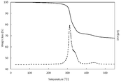
(熱重量分析)
図1に本発明のある実施形態の半導体ナノ粒子複合体の熱分析結果を示す。熱分析は熱重量分析とリガンドの同定より行われる。熱重量分析は、半導体ナノ粒子複合体を、示唆熱重量分析(DTA-TG)を用いて、窒素雰囲気下、10℃/minで550℃まで加熱後、10分保持し、降温する方法で行った。
実線は熱重量分析(TG)の結果であり、破線はTGの微分(ΔTG)の結果である。半導体ナノ粒子複合体を昇温するに従い、リガンドの脱離に起因する質量減少が観測された。500℃以上で質量減少がほぼ一定(10℃あたりの質量減少率が0.15%未満)であることから、半導体ナノ粒子複合体中のリガンドは500℃までに殆ど脱離しており、本実施形態の半導体ナノ粒子全体に占めるリガンド量の割合は32%と算出された。さらに、本実施形態の半導体ナノ粒子複合体の質量減少率(XH)は、350℃以上、550℃以下の範囲で6%であった。なお、半導体ナノ粒子複合体を700℃にまで加熱すると、ほぼ全てのリガンドが半導体ナノ粒子から脱離する。 (Thermogravimetric analysis)
FIG. 1 shows the results of thermal analysis of the semiconductor nanoparticle composite of an embodiment of the present invention. Thermal analysis is performed by thermogravimetric analysis and ligand identification. The thermogravimetric analysis is performed by heating the semiconductor nanoparticle composite to 550 ° C. at 10 ° C./min under a nitrogen atmosphere using differential thermal weight analysis (DTA-TG), holding it for 10 minutes, and lowering the temperature. It was.
The solid line is the result of thermogravimetric analysis (TG), and the broken line is the result of the derivative of TG (ΔTG). As the temperature of the semiconductor nanoparticle composite was raised, a mass loss due to desorption of the ligand was observed. Since the mass loss is almost constant at 500 ° C. or higher (mass loss rate per 10 ° C. is less than 0.15%), the ligand in the semiconductor nanoparticle composite is almost desorbed by 500 ° C. The ratio of the amount of ligand to the total semiconductor nanoparticles in the form was calculated to be 32%. Further, the mass reduction rate ( XH ) of the semiconductor nanoparticle composite of the present embodiment was 6% in the range of 350 ° C. or higher and 550 ° C. or lower. When the semiconductor nanoparticle composite is heated to 700 ° C., almost all the ligands are eliminated from the semiconductor nanoparticles.
本発明の実施形態に係る半導体ナノ粒子複合体は、室温時における半導体ナノ粒子複合体に対する全リガンドの質量分率(L)に対して、熱重量分析において350℃以上、550℃以下の範囲での半導体ナノ粒子複合体の質量減少率(XH)の割合({(XH)/L}×100)が10以上、55以下である。これはすなわち、室温において半導体ナノ粒子に配位している全リガンドのうち、質量の割合にして10~55のリガンドが、室温から350℃までという低温度の範囲ではなく、350℃以上、550℃以下という高温度の範囲で半導体ナノ粒子の表面から離脱するということを意味する。350℃以上、550℃以下という高温度の範囲で半導体ナノ粒子の表面から離脱するリガンドの割合が10~55であることで、高い光学特性を有する半導体ナノ粒子複合体が得られる指標となる。なお、上記の割合({(XH)/L}×100)は10~50であることがより好ましい。
The semiconductor nanoparticle composite according to the embodiment of the present invention has a mass fraction (L) of all ligands with respect to the semiconductor nanoparticle composite at room temperature in a range of 350 ° C. or higher and 550 ° C. or lower in thermal weight analysis. The ratio of the mass reduction rate ( XH ) of the semiconductor nanoparticle composite ({( XH ) / L} × 100) is 10 or more and 55 or less. This means that of all the ligands coordinated to the semiconductor nanoparticles at room temperature, the ligands of 10 to 55 by mass are not in the low temperature range of room temperature to 350 ° C, but 350 ° C or higher and 550. It means that the semiconductor nanoparticles are separated from the surface in the high temperature range of ℃ or less. When the proportion of the ligand that leaves the surface of the semiconductor nanoparticles in the high temperature range of 350 ° C. or higher and 550 ° C. or lower is 10 to 55, it becomes an index for obtaining a semiconductor nanoparticle composite having high optical characteristics. The above ratio ({(X H ) / L} × 100) is more preferably 10 to 50.
また、本発明の別の実施形態に係る半導体ナノ粒子複合体は、半導体ナノ粒子複合体の350℃以上、550℃以下の範囲での質量減少率((350℃~550℃の範囲での半導体ナノ粒子複合体の質量減少量)/(室温での半導体ナノ粒子複合体の質量)×100)は2%以上、15%以下である。質量減少率がこの範囲内にあることで、半導体ナノ粒子複合体は高い蛍光量子効率を有する。
Further, the semiconductor nanoparticle composite according to another embodiment of the present invention has a mass reduction rate of the semiconductor nanoparticle composite in the range of 350 ° C. or higher and 550 ° C. or lower (semiconductor in the range of (350 ° C. to 550 ° C.). (Mass reduction amount of nanoparticle composite) / (mass of semiconductor nanoparticle composite at room temperature) × 100) is 2% or more and 15% or less. When the mass reduction rate is within this range, the semiconductor nanoparticle composite has high fluorescence quantum efficiency.
本発明のある実施形態に係る半導体ナノ粒子複合体は、「半導体ナノ粒子複合体を室温から700℃に加熱した際の質量減少率(X)」に対する「室温から350℃の範囲での質量減少率(XL)」の比(XL/X)と、「室温時における半導体ナノ粒子複合体に対する全リガンドの質量分率(L)」に対する「室温時における半導体ナノ粒子複合体に対する極性リガンドの質量分率(LP)」の比との関係が、(XL/X)<(LP/L)であることが好ましい。
上記の様に(XL/X)<(LP/L)の関係が成立する場合には、350℃以上の高い温度領域でも少なくとも一部の極性リガンドが半導体ナノ粒子から脱離せずに強力に配位していることを意味する。なお、後述するように、脂肪族リガンドは極性リガンドよりも高温領域で半導体ナノ粒子の表面から脱離する。このように半導体ナノ粒子に強力に配位しているリガンドは、室温はもちろんのこと、アプリケーションとして用いられる温度領域においても半導体ナノ粒子の表面に対候性を与えるのに十分な力で半導体ナノ粒子の表面を覆っているため、本発明の実施形態に係る半導体ナノ粒子複合体は高い光学活性を示す。
なお、前述したように、本発明の半導体ナノ粒子複合体は700℃にまで加熱すると、ほぼ全てのリガンドが半導体ナノ粒子から脱離する。このため、「半導体ナノ粒子複合体を室温から700℃に加熱した際の質量減少率(X)」と、「室温時における半導体ナノ粒子複合体に対する半導体ナノ粒子に配位している全リガンドの質量分率(L)」はほぼ同じ値をとる。 The semiconductor nanoparticle composite according to an embodiment of the present invention has a “mass reduction in the range of room temperature to 350 ° C.” with respect to “mass fraction reduction (X) when the semiconductor nanoparticle composite is heated from room temperature to 700 ° C.”. rate as the ratio of (X L) "(X L / X)," polar ligand to semiconductor nanoparticles complex at "room temperature to the total mass fraction of the ligand (L)" with respect to the semiconductor nanoparticle complex at room temperature relationship between the ratio of the mass fraction (L P) "is preferably a (X L / X) <( L P / L).
If the relationship as described above (X L / X) <( L P / L) is established, powerful without at least a portion of the polar ligand desorbed from the semiconductor nanoparticles in more 350 ° C. in a temperature range higher It means that it is coordinated to. As will be described later, the aliphatic ligand desorbs from the surface of the semiconductor nanoparticles in a region higher than that of the polar ligand. The ligand strongly coordinated to the semiconductor nanoparticles in this way has sufficient force to impart weather resistance to the surface of the semiconductor nanoparticles not only at room temperature but also in the temperature range used for applications. Since it covers the surface of the particles, the semiconductor nanoparticle composite according to the embodiment of the present invention exhibits high optical activity.
As described above, when the semiconductor nanoparticle composite of the present invention is heated to 700 ° C., almost all the ligands are eliminated from the semiconductor nanoparticles. Therefore, "mass reduction rate (X) when the semiconductor nanoparticle composite is heated from room temperature to 700 ° C." and "all ligands coordinated to the semiconductor nanoparticles with respect to the semiconductor nanoparticle composite at room temperature". The mass fraction (L) ”has almost the same value.
さらに、上記のΔTGの結果からは310℃付近と430℃付近に2つのピークが確認された。これらは各々リガンドの脱離によるものである。示差熱測定の各ピーク面積に占める面積が2%を超える温度を各リガンドの脱離温度とすると、低温でのリガンドの脱離温度は205℃、高温でのリガンドの脱離温度は394℃と算出される。脱離したリガンドについては赤外線吸収スペクトルを用いて、リガンドの同定を行うことができる。
Furthermore, from the above ΔTG results, two peaks were confirmed around 310 ° C and around 430 ° C. These are due to the elimination of each ligand. Assuming that the temperature at which the area occupied by each peak area of the differential heat measurement exceeds 2% is the desorption temperature of each ligand, the desorption temperature of the ligand at a low temperature is 205 ° C, and the desorption temperature of the ligand at a high temperature is 394 ° C. It is calculated. For the desorbed ligand, the ligand can be identified by using the infrared absorption spectrum.
まず、赤外線吸収スペクトルを用いた半導体ナノ粒子複合体中のリガンドの種類と質量比率の算出方法を記載する。赤外線吸収スペクトルのデータは、日本分光社製FT/IR-4200を用いて、KBr錠剤法により作製した半導体ナノ粒子複合体ペレットに対して収集した。
図2(a)は本実施形態の半導体ナノ粒子複合体の赤外線吸収スペクトルを示したものである。2900cm-1、1450cm-1付近にC-H伸縮、C-H変角の吸収ピークが、1550cm-1付近にC=O伸縮の吸収ピークが、1100cm-1付近にC-O伸縮の吸収ピークがそれぞれ観測された。なお、2300cm-1~2500cm-1に表れる吸収ピークは二酸化炭素によるものである。 First, a method for calculating the type and mass ratio of the ligand in the semiconductor nanoparticle composite using the infrared absorption spectrum will be described. Infrared absorption spectrum data was collected for semiconductor nanoparticle composite pellets prepared by the KBr tablet method using FT / IR-4200 manufactured by JASCO Corporation.
FIG. 2A shows an infrared absorption spectrum of the semiconductor nanoparticle composite of the present embodiment. 2900 cm -1, C-H stretching in the vicinity of 1450 cm -1, the absorption peak of the C-H deformation is, the absorption peak of the C = O stretching in the vicinity of 1550 cm -1 is absorption peak of C-O stretch in the vicinity of 1100 cm -1 Were observed respectively. The absorption peaks appearing in 2300 cm -1 to 2500 cm -1 are due to carbon dioxide.
図2(b)、(c)、(d)は本実施形態の半導体ナノ粒子複合体中に存在すると思われるリガンド単体での赤外線吸収スペクトルを示したものである。本実施形態においては、極性リガンド1種と脂肪族リガンド2種が半導体ナノ粒子に配位している。本実施形態においては、リガンド(b)は極性リガンドであり、リガンド(c)およびリガンド(d)は脂肪族リガンドである。
赤外線吸収スペクトルの吸光度は物質の濃度と厚みのみに比例するため、ピーク面積から定量分析を行うことが可能である。 FIGS. 2 (b), 2 (c), and 2 (d) show infrared absorption spectra of the ligand alone, which is considered to be present in the semiconductor nanoparticle composite of the present embodiment. In this embodiment, one polar ligand and two aliphatic ligands are coordinated to the semiconductor nanoparticles. In this embodiment, the ligand (b) is a polar ligand, and the ligand (c) and the ligand (d) are aliphatic ligands.
Since the absorbance of the infrared absorption spectrum is proportional only to the concentration and thickness of the substance, it is possible to perform quantitative analysis from the peak area.
一般に、半導体ナノ粒子複合体の赤外線吸収スペクトルをSQD(ν)、i番目の脂肪族リガンドの赤外線吸収スペクトルをSai(ν)、i番目の極性リガンドの赤外線吸収スペクトルをSpi(ν)とすると、式(1)のように表される。
SQD(ν)= ΣaiSai(ν) + ΣpiSpi(ν) 式(1)
ここで、νは波数であり、aiおよびpiはそれぞれ脂肪族リガンドおよび極性リガンドのモル分率に関係する定数である。 Generally, the infrared absorption spectrum of the semiconductor nanoparticle conjugate S QD (ν), the infrared absorption spectrum of the i-th aliphatic ligand S ai (ν), the infrared absorption spectrum of the i-th polar ligand S pi (ν) Then, it is expressed as the equation (1).
S QD (ν) = ΣaiS ai (ν) + ΣpiS pi (ν) Equation (1)
Here, ν is a wave number, and ai and pi are constants related to the mole fraction of the aliphatic ligand and the polar ligand, respectively.
例えば、本実施形態の半導体ナノ粒子複合体の赤外線吸収スペクトルは(b)の極性リガンドのスペクトルをS(b)(ν)とし、(c)および(d)の脂肪族リガンドのスペクトルをそれぞれS(c)(ν)、S(d)(ν)とすると、式(2)のように表される。
SQD(ν)= bS(b)(ν) + cS(c)(ν) + dS(d)(ν) 式(2)
ここで、νは波数、b、cおよびdはそれぞれ定数である。実測値と計算値の残差平方和が最も小さくなるような定数b、cおよびdの値を、エクセル(マイクロソフト社製表計算ソフト)のソルバー機能を用いて決定した。図3は赤外線吸収スペクトルの実測値と計算値をフィッティングしたものである。点線が実測値、実線が計算値である。計算値はよく実測値を表現していることがわかる。 For example, in the infrared absorption spectrum of the semiconductor nanoparticle composite of the present embodiment, the spectrum of the polar ligand of (b) is S (b) (ν), and the spectra of the aliphatic ligands of (c) and (d) are S, respectively. If (c) (ν) and S (d) (ν), it is expressed as in the equation (2).
S QD (ν) = bS (b) (ν) + cS (c) (ν) + dS (d) (ν) Equation (2)
Here, ν is a wave number, and b, c, and d are constants. The values of the constants b, c, and d that minimize the residual sum of squares of the measured value and the calculated value were determined using the solver function of Excel (spreadsheet software manufactured by Microsoft Corporation). FIG. 3 is a fitting of the measured value and the calculated value of the infrared absorption spectrum. The dotted line is the measured value and the solid line is the calculated value. It can be seen that the calculated values often represent the measured values.
図4はC-H伸縮の吸収ピークの、フィッティングカーブに占める各リガンド成分の赤外線吸収スペクトルの構成である。図4においては、図3及び図2と同様に、点線が半導体ナノ粒子複合体の赤外線吸収スペクトル実測値を示し、グレーの実線はリガンド(b)の赤外線吸収スペクトルの実測値を示し、2本のグレーの破線はそれぞれリガンド(c)と(d)の赤外線吸収スペクトル実測値を示している。黒の実線が計算値であり、計算値はよく実測値を表現していることがわかる。C-H伸縮の吸収ピークは半導体ナノ粒子複合体中の全てのリガンド成分の吸収を含むため、波形分離により得られる各リガンド成分のピーク面積比から、リガンドの組成を求めることができる。各リガンド成分の質量分率は、前記ピーク面積比と、分子内のプロトン数、および分子量から計算した。図4は、後述する例1により得られた半導体ナノ粒子複合体の測定結果を示すものであるが、この例では、リガンド成分の質量分率はリガンド(b):リガンド(c):リガンド(d)=89:8:3であり、すなわち、極性リガンド(b)と脂肪族リガンド((c)+(d))の質量比は89:11であることが算出できる。
FIG. 4 shows the composition of the infrared absorption spectrum of each ligand component in the fitting curve of the absorption peak of CH expansion and contraction. In FIG. 4, as in FIGS. 3 and 2, the dotted line shows the measured infrared absorption spectrum of the semiconductor nanoparticle composite, and the gray solid line shows the measured infrared absorption spectrum of the ligand (b). The gray broken lines in are shown by the measured infrared absorption spectra of the ligands (c) and (d), respectively. It can be seen that the solid black line is the calculated value, and the calculated value often represents the measured value. Since the absorption peak of CH expansion and contraction includes the absorption of all the ligand components in the semiconductor nanoparticle complex, the composition of the ligand can be obtained from the peak area ratio of each ligand component obtained by waveform separation. The mass fraction of each ligand component was calculated from the peak area ratio, the number of protons in the molecule, and the molecular weight. FIG. 4 shows the measurement results of the semiconductor nanoparticle complex obtained in Example 1 described later. In this example, the mass fraction of the ligand component is ligand (b): ligand (c): ligand ( It can be calculated that d) = 89: 8: 3, that is, the mass ratio of the polar ligand (b) to the aliphatic ligand ((c) + (d)) is 89:11.
上述した方法を用いて、熱分析において低温で脱離したリガンドの同定を行う。
図5に、熱処理前後の本実施形態の半導体ナノ粒子複合体の赤外線吸収スペクトルを示す。実線は熱処理前の半導体ナノ粒子複合体の赤外線吸収スペクトルであり、破線は窒素雰囲気下で10℃/minで350℃まで加熱し、室温に冷却した半導体ナノ粒子複合体の赤外線吸収スペクトルである。
熱処理前の半導体ナノ粒子複合体の赤外線吸収スペクトルでは、1100cm-1付近にC-O伸縮の鋭い吸収ピークが観測される一方で、350℃まで加熱した半導体ナノ粒子複合体ではこのピーク強度がかなり弱くなっていることがわかる。350℃まで加熱した半導体ナノ粒子複合体には2900cm-1、1450cm-1付近のC-H伸縮、C-H変角の吸収ピークが強く観測されることから、ΔTGで確認された低温で脱離したリガンドは極性リガンド(b)に帰属され、350℃以上の高温脱離成分は脂肪族リガンド(c)および(d)に帰属するといえる。なお、上述したように、2300cm-1~2500cm-1に表れる吸収ピークは二酸化炭素によるものである。 The method described above is used to identify ligands desorbed at low temperatures in thermal analysis.
FIG. 5 shows an infrared absorption spectrum of the semiconductor nanoparticle composite of the present embodiment before and after the heat treatment. The solid line is the infrared absorption spectrum of the semiconductor nanoparticle composite before heat treatment, and the broken line is the infrared absorption spectrum of the semiconductor nanoparticle composite heated to 350 ° C. at 10 ° C./min in a nitrogen atmosphere and cooled to room temperature.
In the infrared absorption spectrum of the semiconductor nanoparticle composite before heat treatment, a sharp absorption peak of CO expansion and contraction is observed around 1100 cm -1 , while this peak intensity is considerably high in the semiconductor nanoparticle composite heated to 350 ° C. You can see that it is getting weaker. 350 ° C. 2900 cm -1 in the semiconductor nanoparticle complexes heated to, C-H stretching in the vicinity of 1450 cm -1, since the absorption peak of the C-H bending is strongly observed, de-cold confirmed in ΔTG It can be said that the separated ligand belongs to the polar ligand (b), and the high-temperature desorption component at 350 ° C. or higher belongs to the aliphatic ligands (c) and (d). As described above, the absorption peaks appearing in 2300 cm -1 to 2500 cm -1 are due to carbon dioxide.
室温時における半導体ナノ粒子複合体に対する全リガンドの質量分率(L)の算出方法は次の通りである。
上記の熱重量分析において、半導体ナノ粒子複合体の質量減少量がほぼ一定となる点を終点とすると、終点までの質量減少量が室温時に半導体ナノ粒子に配位している全リガンド量を示している。なお、半導体ナノ粒子に配位しているリガンドの種類によってリガンドの脱離温度が変わる。このため、室温時における半導体ナノ粒子複合体に対する全リガンドの質量分率(L)を算出するためには、加熱温度を700℃以上としたときの熱重量分析結果(質量減少量)を用いて判断すればよい。 The method for calculating the mass fraction (L) of all ligands with respect to the semiconductor nanoparticle composite at room temperature is as follows.
In the above thermal weight analysis, assuming that the end point is the point where the mass reduction amount of the semiconductor nanoparticle composite is almost constant, the mass reduction amount up to the end point indicates the total amount of ligands coordinated to the semiconductor nanoparticles at room temperature. ing. The desorption temperature of the ligand changes depending on the type of ligand coordinated to the semiconductor nanoparticles. Therefore, in order to calculate the mass fraction (L) of all ligands with respect to the semiconductor nanoparticle composite at room temperature, the thermogravimetric analysis result (mass reduction amount) when the heating temperature is 700 ° C. or higher is used. You just have to judge.
以上の熱重量分析の測定結果、および赤外線吸収スペクトルの測定結果より、本願記載の半導体ナノ粒子複合体を加熱すると、脂肪族リガンドが極性リガンドよりも高温で半導体ナノ粒子の表面から脱離するという特徴があることが分かる。さらに、350℃以上で脱離する成分の少なくとも一部は脂肪族リガンドに帰属する。
参考として、非特許文献6に記載の脂肪族リガンド(ドデカンチオール)は結合したZnから250℃~300℃程度で脱離することが開示されている。本願に記載の半導体ナノ粒子複合体中の脂肪族リガンドの脱離温度は文献と比較して高い温度である。
リガンドの脱離温度は、化学構造のみならず、半導体ナノ粒子表面に存在するZnとの配位形態や、リガンドの結晶構造形成など、周囲の原子・分子との相互作用に大きな影響を受けると考えられ、本願に記載の半導体ナノ粒子に配位している脂肪族リガンドは、前述したような因子により半導体ナノ粒子表面で強い束縛を受け、高い脱離温度を示す。このように半導体ナノ粒子表面で強い束縛を受けた脂肪族リガンドの存在が半導体ナノ粒子の蛍光量子効率を向上させると、発明者らは推測している。前述した脂肪族リガンドの存在は耐熱性を向上させる効果もあると発明者らは推測している。 Based on the above measurement results of thermoweight analysis and infrared absorption spectrum, it is said that when the semiconductor nanoparticle composite described in the present application is heated, the aliphatic ligand is desorbed from the surface of the semiconductor nanoparticles at a temperature higher than that of the polar ligand. It turns out that there is a feature. Furthermore, at least a part of the components desorbed at 350 ° C. or higher is attributed to the aliphatic ligand.
As a reference, it is disclosed that the aliphatic ligand (dodecanethiol) described in Non-Patent Document 6 is eliminated from the bound Zn at about 250 ° C. to 300 ° C. The desorption temperature of the aliphatic ligand in the semiconductor nanoparticle complex described in the present application is higher than that in the literature.
The desorption temperature of the ligand is greatly affected not only by the chemical structure but also by the interaction with surrounding atoms and molecules, such as the coordination form with Zn existing on the surface of the semiconductor nanoparticles and the formation of the crystal structure of the ligand. It is conceivable that the aliphatic ligand coordinated to the semiconductor nanoparticles described in the present application is strongly bound on the surface of the semiconductor nanoparticles due to the factors as described above, and exhibits a high desorption temperature. The inventors speculate that the presence of such a strongly bound aliphatic ligand on the surface of the semiconductor nanoparticles improves the fluorescence quantum efficiency of the semiconductor nanoparticles. The inventors speculate that the presence of the above-mentioned aliphatic ligand also has the effect of improving heat resistance.
本発明の半導体ナノ粒子複合体は、以下の構成を採用する。
(1)半導体ナノ粒子の表面に、脂肪族リガンドと極性リガンドを含む2種以上のリガンドが配位した半導体ナノ粒子複合体であって、
前記リガンドは有機基と配位性基とからなり、
前記脂肪族リガンドは、前記有機基が脂肪族炭化水素基であり、
前記極性リガンドは、前記有機基に親水性官能基を含み、
前記脂肪族リガンドと前記極性リガンドとの質量比(脂肪族リガンド/極性リガンド)が0.05~1.00であり、
室温時における半導体ナノ粒子複合体に対する全リガンドの質量分率(L)に対して、熱重量分析において350℃以上、550℃以下の範囲での半導体ナノ粒子複合体の質量減少率(XH)の割合({(XH)/L}×100)が10以上、55以下である、
半導体ナノ粒子複合体。
(2)半導体ナノ粒子の表面に、脂肪族リガンドと極性リガンドを含む2種以上のリガンドが配位した半導体ナノ粒子複合体であって、
前記リガンドは有機基と配位性基とからなり、
前記脂肪族リガンドは、前記有機基が脂肪族炭化水素基であり、
前記極性リガンドは、前記有機基に親水性官能基を含み、
前記脂肪族リガンドと前記極性リガンドとの質量比(脂肪族リガンド/極性リガンド)が0.05~1.00であり、
熱重量分析において350℃以上、550℃以下の範囲での半導体ナノ粒子複合体の質量減少率(XH)が2%以上、15%以下である、
半導体ナノ粒子複合体。
(3)前記半導体ナノ粒子複合体を加熱した際、前記極性リガンドが前記脂肪族リガンドより低温で前記半導体ナノ粒子の表面から脱離する、
上記(1)または(2)に記載の半導体ナノ粒子複合体。
(4)前記熱重量分析において、
半導体ナノ粒子複合体を室温から700℃に加熱した際の質量減少率(X)に対する、室温から350℃の範囲での質量減少率(XL)の比(XL/X)と、
室温時における半導体ナノ粒子複合体に対する全リガンドの質量分率(L)に対する、室温時における半導体ナノ粒子複合体に対する極性リガンドの質量分率(LP)の比(LP/L)と、の関係が、
(XL/X)<(LP/L)である、
上記(1)~(3)のいずれか一項に記載の半導体ナノ粒子複合体。
(5)前記半導体ナノ粒子複合体は、SP値9.0~15.0の分散媒に分散可能である、
上記(1)~(4)のいずれか一項に記載の半導体ナノ粒子複合体。
(6)前記分散媒が、アセトン、PGMEA、PGME、IPA、エタノール、およびメタノールからなる群より選択される1種または2種以上の混合分散媒である、
上記(5)に記載の半導体ナノ粒子複合体。
(7)前記350℃以上での質量減少の少なくとも一部が、前記脂肪族リガンドの脱離に帰属される、
上記(1)~(6)のいずれか一項に記載の半導体ナノ粒子複合体。
(8)前記脂肪族リガンドは、1つの配位性基と、少なくとも1つ以上の脂肪族炭化水素基が結合している、
上記(1)~(7)のいずれか一項に記載の半導体ナノ粒子複合体。
(9)前記極性リガンドの分子量が50以上、600以下である、
上記(1)~(8)のいずれか一項に記載の半導体ナノ粒子複合体。
(10)前記極性リガンドの分子量が50以上、450以下である、
上記(1)~(9)のいずれか一項に記載の半導体ナノ粒子複合体。
(11)前記脂肪族リガンドの配位性基が、アミノ基、カルボキシル基、メルカプト基、ホスフィン基、およびホスフィンオキシド基からなる群より選ばれる、
上記(1)~(10)のいずれか一項に記載の半導体ナノ粒子複合体。
(12)前記極性リガンドの有機基が、ヒドロキシル基、カルボキシル基、カルボニル基、メルカプト基、アミノ基、エーテル結合、エステル結合、およびシロキサン結合のうち少なくとも一つを有する、
上記(1)~(11)のいずれか一項に記載の半導体ナノ粒子複合体。
(13)前記極性リガンドの配位性基がメルカプト基である、
上記(1)~(12)のいずれか一項に記載の半導体ナノ粒子複合体。
(14)前記半導体ナノ粒子に対する前記リガンドの質量比(リガンド/半導体ナノ粒子)が、0.1~0.7である、
上記(1)~(13)のいずれか一項に記載の半導体ナノ粒子複合体。
(15)前記半導体ナノ粒子に対する前記リガンドの質量比(リガンド/半導体ナノ粒子)が、0.1~0.5である、
上記(1)~(14)のいずれか一項に記載の半導体ナノ粒子複合体。
(16)前記半導体ナノ粒子の質量分率で25質量%以上となるように前記分散媒に分散可能である、
上記(5)~(15)のいずれか一項に記載の半導体ナノ粒子複合体。
(17)前記半導体ナノ粒子の質量分率で35質量%以上となるように前記分散媒に分散可能である、
上記(5)~(16)のいずれか一項に記載の半導体ナノ粒子複合体。
(18)前記半導体ナノ粒子は前記半導体ナノ粒子の表面にZnを含有する、
上記(1)~(17)のいずれか一項に記載の半導体ナノ粒子複合体。
(19)前記半導体ナノ粒子複合体の蛍光量子効率が80%以上である、
上記(1)~(18)のいずれか一項に記載の半導体ナノ粒子複合体。
(20)前記半導体ナノ粒子複合体の発光スペクトルの半値幅が40nm以下である、
上記(1)~(19)のいずれか一項に記載の半導体ナノ粒子複合体。
(21)前記半導体ナノ粒子がInおよびPを含む、
上記(1)~(20)のいずれか一項に記載の半導体ナノ粒子複合体。 The semiconductor nanoparticle composite of the present invention adopts the following constitution.
(1) A semiconductor nanoparticle complex in which two or more ligands including an aliphatic ligand and a polar ligand are coordinated on the surface of semiconductor nanoparticles.
The ligand consists of an organic group and a coordinating group.
In the aliphatic ligand, the organic group is an aliphatic hydrocarbon group.
The polar ligand contains a hydrophilic functional group in the organic group.
The mass ratio of the aliphatic ligand to the polar ligand (aliphatic ligand / polar ligand) is 0.05 to 1.00.
Mass fraction (X H ) of the semiconductor nanoparticle composite in the range of 350 ° C. or higher and 550 ° C. or lower in the thermal weight analysis with respect to the mass fraction (L) of all ligands with respect to the semiconductor nanoparticle composite at room temperature. ({( XH ) / L} × 100) is 10 or more and 55 or less.
Semiconductor nanoparticle composite.
(2) A semiconductor nanoparticle complex in which two or more kinds of ligands including an aliphatic ligand and a polar ligand are coordinated on the surface of the semiconductor nanoparticles.
The ligand consists of an organic group and a coordinating group.
In the aliphatic ligand, the organic group is an aliphatic hydrocarbon group.
The polar ligand contains a hydrophilic functional group in the organic group.
The mass ratio of the aliphatic ligand to the polar ligand (aliphatic ligand / polar ligand) is 0.05 to 1.00.
In the thermogravimetric analysis, the mass reduction rate ( XH ) of the semiconductor nanoparticle composite in the range of 350 ° C. or higher and 550 ° C. or lower is 2% or more and 15% or less.
Semiconductor nanoparticle composite.
(3) When the semiconductor nanoparticle composite is heated, the polar ligand is desorbed from the surface of the semiconductor nanoparticles at a lower temperature than the aliphatic ligand.
The semiconductor nanoparticle composite according to (1) or (2) above.
(4) In the thermogravimetric analysis
The ratio ( XL / X) of the mass loss rate ( XL ) in the range of room temperature to 350 ° C. to the mass loss rate (X) when the semiconductor nanoparticle composite is heated from room temperature to 700 ° C.
Mass fraction of total ligand to semiconductor nanoparticles complex at room temperature for (L), the mass fraction of polar ligand to semiconductor nanoparticles complex at room temperature with (L P) ratio (L P / L), the Relationship,
(X L / X) is <(L P / L),
The semiconductor nanoparticle composite according to any one of (1) to (3) above.
(5) The semiconductor nanoparticle composite can be dispersed in a dispersion medium having an SP value of 9.0 to 15.0.
The semiconductor nanoparticle composite according to any one of (1) to (4) above.
(6) The dispersion medium is one or more mixed dispersion media selected from the group consisting of acetone, PGMEA, PGME, IPA, ethanol, and methanol.
The semiconductor nanoparticle composite according to (5) above.
(7) At least a part of the mass loss at 350 ° C. or higher is attributed to the elimination of the aliphatic ligand.
The semiconductor nanoparticle composite according to any one of (1) to (6) above.
(8) The aliphatic ligand has one coordinating group and at least one or more aliphatic hydrocarbon groups bonded thereto.
The semiconductor nanoparticle composite according to any one of (1) to (7) above.
(9) The molecular weight of the polar ligand is 50 or more and 600 or less.
The semiconductor nanoparticle composite according to any one of (1) to (8) above.
(10) The molecular weight of the polar ligand is 50 or more and 450 or less.
The semiconductor nanoparticle composite according to any one of (1) to (9) above.
(11) The coordinating group of the aliphatic ligand is selected from the group consisting of an amino group, a carboxyl group, a mercapto group, a phosphine group, and a phosphine oxide group.
The semiconductor nanoparticle composite according to any one of (1) to (10) above.
(12) The organic group of the polar ligand has at least one of a hydroxyl group, a carboxyl group, a carbonyl group, a mercapto group, an amino group, an ether bond, an ester bond, and a siloxane bond.
The semiconductor nanoparticle composite according to any one of (1) to (11) above.
(13) The coordinating group of the polar ligand is a mercapto group.
The semiconductor nanoparticle composite according to any one of (1) to (12) above.
(14) The mass ratio of the ligand to the semiconductor nanoparticles (ligand / semiconductor nanoparticles) is 0.1 to 0.7.
The semiconductor nanoparticle composite according to any one of (1) to (13) above.
(15) The mass ratio of the ligand to the semiconductor nanoparticles (ligand / semiconductor nanoparticles) is 0.1 to 0.5.
The semiconductor nanoparticle composite according to any one of (1) to (14) above.
(16) The semiconductor nanoparticles can be dispersed in the dispersion medium so as to have a mass fraction of 25% by mass or more.
The semiconductor nanoparticle composite according to any one of (5) to (15) above.
(17) The semiconductor nanoparticles can be dispersed in the dispersion medium so as to have a mass fraction of 35% by mass or more.
The semiconductor nanoparticle composite according to any one of (5) to (16) above.
(18) The semiconductor nanoparticles contain Zn on the surface of the semiconductor nanoparticles.
The semiconductor nanoparticle composite according to any one of (1) to (17) above.
(19) The fluorescence quantum efficiency of the semiconductor nanoparticle composite is 80% or more.
The semiconductor nanoparticle composite according to any one of (1) to (18) above.
(20) The half width of the emission spectrum of the semiconductor nanoparticle composite is 40 nm or less.
The semiconductor nanoparticle composite according to any one of (1) to (19) above.
(21) The semiconductor nanoparticles contain In and P.
The semiconductor nanoparticle composite according to any one of (1) to (20) above.
(均等論)
本明細書に記載の構成および/または方法は例として示され、多数の変形形態が可能であるため、これらの具体例または実施例は限定の意味であると見なすべきではないことが理解されよう。本明細書に記載の特定の手順または方法は、多数の処理方法の1つを表しうる。したがって、説明および/または記載される種々の行為は、説明および/または記載される順序で行うことができ、または省略することもできる。同様に前述の方法の順序は変更可能である。
本開示の主題は、本明細書に開示される種々の方法、システムおよび構成、並びにほかの特徴、機能、行為、および/または性質のあらゆる新規のかつ自明でない組み合わせおよび副次的組み合わせ、並びにそれらのあらゆる均等物を含む。 (Doctrine of equivalents)
It will be appreciated that the configurations and / or methods described herein are illustrated by way of example and that a number of variants are possible and that these embodiments or examples should not be considered as limiting. .. The particular procedure or method described herein may represent one of a number of processing methods. Thus, the various acts described and / or described may be performed in the order described and / or described, or may be omitted. Similarly, the order of the above methods can be changed.
The subject matter of this disclosure is the various methods, systems and configurations disclosed herein, as well as any new and non-trivial combinations and secondary combinations of other features, functions, actions, and / or properties, as well as them. Including any equivalent of.
以下、実施例および比較例により本発明を具体的に説明するが、本発明はこれらに限定されるものではない。
Hereinafter, the present invention will be specifically described with reference to Examples and Comparative Examples, but the present invention is not limited thereto.
[例1]
まず、以下の方法に従って、半導体ナノ粒子の合成を行った。
(前駆体の作製)
<Zn前駆体溶液の調製>
40mmolのオレイン酸亜鉛と75mLのオクタデセンを混合し、真空化で110℃にて1時間加熱し、[Zn]=0.4MのZn前駆体を調製した。
<Se前駆体(セレン化トリオクチルホスフィン)の調製)>
22mmolのセレン粉末と10mLのトリオクチルホスフィンを窒素中で混合し、全て溶けるまで撹拌して[Se]=2.2Mのセレン化トリオクチルホスフィンを得た。
<S前駆体(硫化トリオクチルホスフィン)の調製>
22mmolの硫黄粉末と10mLのトリオクチルホスフィンを窒素中で混合し、全て溶けるまで撹拌して[S]=2.2Mの硫化トリオクチルホスフィンを得た。 [Example 1]
First, semiconductor nanoparticles were synthesized according to the following method.
(Preparation of precursor)
<Preparation of Zn precursor solution>
40 mmol of zinc oleate and 75 mL of octadecene were mixed and heated in vacuum at 110 ° C. for 1 hour to prepare a Zn precursor of [Zn] = 0.4 M.
<Preparation of Se precursor (selenate trioctylphosphine)>
22 mmol of selenium powder and 10 mL of trioctylphosphine were mixed in nitrogen and stirred until all were dissolved to give [Se] = 2.2 M selenium trioctylphosphine.
<Preparation of S precursor (trioctylphosphine sulfide)>
22 mmol of sulfur powder and 10 mL of trioctylphosphine were mixed in nitrogen and stirred until all were dissolved to give [S] = 2.2 M trioctylphosphine sulfide.
(半導体ナノ粒子の合成)
酢酸インジウム(0.3mmol)とオレイン酸亜鉛(0.6mmol)を、オレイン酸(0.9mmol)と1-ドデカンチオール(0.1mmol)とオクタデセン(10mL)の混合物に加え、真空下(<20Pa)で約120℃に加熱し、1時間反応させた。真空下で反応させた混合物を25℃、窒素雰囲気下にして、トリス(トリメチルシリル)ホスフィン(0.2mmol)を加えたのち、約300℃に加熱し、10分間反応させた。反応液を25℃に冷却し、オクタン酸クロリド(0.45mmol)を注入し、約250℃で30分間加熱後、25℃に冷却した。
その後、200℃まで加熱し、0.75mLのZn前駆体溶液、0.3mmolのセレン化トリオクチルホスフィンを同時に添加し、30分間反応させInP系半導体ナノ粒子の表面にZnSeシェルを形成した。さらに、1.5mLのZn前駆体溶液と0.6mmolの硫化トリオクチルホスフィンを添加し、250℃に昇温して1時間反応させZnSシェルを形成した。
上記のように合成して得られた半導体ナノ粒子の反応溶液をアセトンに加え、良く混合したのち遠心分離した。遠心加速度は4000Gとした。沈殿物を回収し、沈殿物にノルマルヘキサンを加え、分散液を作製した。この操作を数回繰り返し、精製した半導体ナノ粒子を得た。 (Semiconductor nanoparticles synthesis)
Indium acetate (0.3 mmol) and zinc oleate (0.6 mmol) are added to a mixture of oleic acid (0.9 mmol), 1-dodecanethiol (0.1 mmol) and octadecene (10 mL) under vacuum (<20 Pa). ) Was heated to about 120 ° C. and reacted for 1 hour. The mixture reacted under vacuum was placed in a nitrogen atmosphere at 25 ° C., tris (trimethylsilyl) phosphine (0.2 mmol) was added, and then the mixture was heated to about 300 ° C. and reacted for 10 minutes. The reaction mixture was cooled to 25 ° C., octanoic acid chloride (0.45 mmol) was injected, heated at about 250 ° C. for 30 minutes, and then cooled to 25 ° C.
Then, the mixture was heated to 200 ° C., 0.75 mL of a Zn precursor solution and 0.3 mmol of selenate trioctylphosphine were simultaneously added, and the mixture was reacted for 30 minutes to form a ZnSe shell on the surface of InP-based semiconductor nanoparticles. Further, 1.5 mL of a Zn precursor solution and 0.6 mmol of trioctylphosphine sulfide were added, and the temperature was raised to 250 ° C. and reacted for 1 hour to form a ZnS shell.
The reaction solution of the semiconductor nanoparticles obtained by the synthesis as described above was added to acetone, mixed well, and then centrifuged. The centrifugal acceleration was 4000 G. The precipitate was recovered, and normal hexane was added to the precipitate to prepare a dispersion. This operation was repeated several times to obtain purified semiconductor nanoparticles.
続いて、以下の方法に従って、半導体ナノ粒子複合体の合成を行った。
(リガンド単体の作製)
<PEG-SHの調製>
フラスコに210gのメトキシPEG-OH(分子量400)および93gのトリエチルアミンを収め、420mLのTHF(テトラヒドロフラン)に溶解させた。溶液を0℃に冷却し、反応熱で反応溶液の温度が5℃を超えないよう注意しながら、窒素雰囲気下で51gのメタンスルホン酸クロリドを徐々に滴下した。その後、反応溶液を室温に昇温し2時間撹拌した。この溶液をクロロホルム-水系で抽出し、有機相を回収した。得られた溶液をエバポレーションにより濃縮し、硫酸マグネシウムでオイル状の中間体を得た。これを別の1Lフラスコに移し、窒素雰囲気下で400mLの1.3Mのチオ尿素水溶液を加えた。溶液を2時間還流したのち、21gのNaOHを加え、さらに1.5時間還流した。反応溶液を室温まで冷却し、1M HCl水溶液をpH=7になるまで加え、中和した。得られた溶液をクロロホルム-水系で抽出し、目的とするリガンド(PEG-SH、分子量430)を得た。
分子量400のPEG-SHを合成する工程で、PEG-SHメトキシPEG-OH(分子量400、210g)をメトキシPEG-OH(分子量600、315g)に変えた以外は同様の方法で、分子量600のPEG-SHを得た。
<N-アセチル-N-(2-メルカプトエチル)プロパンアミドの調製>
1.2g(10mmol)のN-(2-sulfanylethyl)acetamideおよび1.7mL(12mmol)のトリエチルアミンを100mLの丸底フラスコに収め、30mLの脱水ジクロロメタンに溶解させた。溶液を0℃に冷却し、窒素雰囲気下で0.87mL(10mmol)のプロパノイルクロリドを、溶液の温度が5℃以上にならないよう注意しながらゆっくりと滴下した。滴下終了後、反応溶液を室温まで昇温し、2時間撹拌した。反応溶液を濾過し、濾液をクロロホルムで希釈した。溶液を10%HCl水溶液、10%Na2CO3水溶液、飽和NaCl水溶液の順に抽出し有機相を回収した。有機相をエバポレーションで濃縮したのち、ヘキサン-酢酸エチル混合溶媒を展開溶媒としたカラムクロマトグラフィーにて精製し、目的物を得た。 Subsequently, the semiconductor nanoparticle composite was synthesized according to the following method.
(Making a single ligand)
<Preparation of PEG-SH>
The flask contained 210 g of methoxyPEG-OH (molecular weight 400) and 93 g of triethylamine and was dissolved in 420 mL of THF (tetrahydrofuran). The solution was cooled to 0 ° C., and 51 g of methanesulfonic acid chloride was gradually added dropwise under a nitrogen atmosphere, taking care that the temperature of the reaction solution did not exceed 5 ° C. due to the heat of reaction. Then, the reaction solution was heated to room temperature and stirred for 2 hours. This solution was extracted with a chloroform-aqueous system to recover the organic phase. The obtained solution was concentrated by evaporation to obtain an oily intermediate with magnesium sulfate. This was transferred to another 1 L flask, and 400 mL of 1.3 M aqueous thiourea solution was added under a nitrogen atmosphere. After refluxing the solution for 2 hours, 21 g of NaOH was added and the mixture was refluxed for another 1.5 hours. The reaction solution was cooled to room temperature and 1M aqueous HCl was added until pH = 7 to neutralize. The obtained solution was extracted with a chloroform-aqueous system to obtain the desired ligand (PEG-SH, molecular weight 430).
In the step of synthesizing PEG-SH having a molecular weight of 400, PEG having a molecular weight of 600 is used in the same manner except that PEG-SH methoxyPEG-OH (molecular weight 400, 210 g) is changed to methoxy PEG-OH (molecular weight 600, 315 g). -SH was obtained.
<Preparation of N-acetyl-N- (2-mercaptoethyl) propanamide>
1.2 g (10 mmol) of N- (2-sulfanylethyl) acetamide and 1.7 mL (12 mmol) of triethylamine were placed in a 100 mL round bottom flask and dissolved in 30 mL of dehydrated dichloromethane. The solution was cooled to 0 ° C. and 0.87 mL (10 mmol) of propanoyl chloride was slowly added dropwise under a nitrogen atmosphere, taking care that the temperature of the solution did not exceed 5 ° C. After completion of the dropping, the reaction solution was heated to room temperature and stirred for 2 hours. The reaction solution was filtered and the filtrate was diluted with chloroform. The solution was extracted in the order of 10% HCl aqueous solution, 10% Na 2 CO 3 aqueous solution, and saturated NaCl aqueous solution, and the organic phase was recovered. The organic phase was concentrated by evaporation and then purified by column chromatography using a hexane-ethyl acetate mixed solvent as a developing solvent to obtain the desired product.
(リガンド単体の作製)
<PEG-SHの調製>
フラスコに210gのメトキシPEG-OH(分子量400)および93gのトリエチルアミンを収め、420mLのTHF(テトラヒドロフラン)に溶解させた。溶液を0℃に冷却し、反応熱で反応溶液の温度が5℃を超えないよう注意しながら、窒素雰囲気下で51gのメタンスルホン酸クロリドを徐々に滴下した。その後、反応溶液を室温に昇温し2時間撹拌した。この溶液をクロロホルム-水系で抽出し、有機相を回収した。得られた溶液をエバポレーションにより濃縮し、硫酸マグネシウムでオイル状の中間体を得た。これを別の1Lフラスコに移し、窒素雰囲気下で400mLの1.3Mのチオ尿素水溶液を加えた。溶液を2時間還流したのち、21gのNaOHを加え、さらに1.5時間還流した。反応溶液を室温まで冷却し、1M HCl水溶液をpH=7になるまで加え、中和した。得られた溶液をクロロホルム-水系で抽出し、目的とするリガンド(PEG-SH、分子量430)を得た。
分子量400のPEG-SHを合成する工程で、PEG-SHメトキシPEG-OH(分子量400、210g)をメトキシPEG-OH(分子量600、315g)に変えた以外は同様の方法で、分子量600のPEG-SHを得た。
<N-アセチル-N-(2-メルカプトエチル)プロパンアミドの調製>
1.2g(10mmol)のN-(2-sulfanylethyl)acetamideおよび1.7mL(12mmol)のトリエチルアミンを100mLの丸底フラスコに収め、30mLの脱水ジクロロメタンに溶解させた。溶液を0℃に冷却し、窒素雰囲気下で0.87mL(10mmol)のプロパノイルクロリドを、溶液の温度が5℃以上にならないよう注意しながらゆっくりと滴下した。滴下終了後、反応溶液を室温まで昇温し、2時間撹拌した。反応溶液を濾過し、濾液をクロロホルムで希釈した。溶液を10%HCl水溶液、10%Na2CO3水溶液、飽和NaCl水溶液の順に抽出し有機相を回収した。有機相をエバポレーションで濃縮したのち、ヘキサン-酢酸エチル混合溶媒を展開溶媒としたカラムクロマトグラフィーにて精製し、目的物を得た。 Subsequently, the semiconductor nanoparticle composite was synthesized according to the following method.
(Making a single ligand)
<Preparation of PEG-SH>
The flask contained 210 g of methoxyPEG-OH (molecular weight 400) and 93 g of triethylamine and was dissolved in 420 mL of THF (tetrahydrofuran). The solution was cooled to 0 ° C., and 51 g of methanesulfonic acid chloride was gradually added dropwise under a nitrogen atmosphere, taking care that the temperature of the reaction solution did not exceed 5 ° C. due to the heat of reaction. Then, the reaction solution was heated to room temperature and stirred for 2 hours. This solution was extracted with a chloroform-aqueous system to recover the organic phase. The obtained solution was concentrated by evaporation to obtain an oily intermediate with magnesium sulfate. This was transferred to another 1 L flask, and 400 mL of 1.3 M aqueous thiourea solution was added under a nitrogen atmosphere. After refluxing the solution for 2 hours, 21 g of NaOH was added and the mixture was refluxed for another 1.5 hours. The reaction solution was cooled to room temperature and 1M aqueous HCl was added until pH = 7 to neutralize. The obtained solution was extracted with a chloroform-aqueous system to obtain the desired ligand (PEG-SH, molecular weight 430).
In the step of synthesizing PEG-SH having a molecular weight of 400, PEG having a molecular weight of 600 is used in the same manner except that PEG-SH methoxyPEG-OH (
<Preparation of N-acetyl-N- (2-mercaptoethyl) propanamide>
1.2 g (10 mmol) of N- (2-sulfanylethyl) acetamide and 1.7 mL (12 mmol) of triethylamine were placed in a 100 mL round bottom flask and dissolved in 30 mL of dehydrated dichloromethane. The solution was cooled to 0 ° C. and 0.87 mL (10 mmol) of propanoyl chloride was slowly added dropwise under a nitrogen atmosphere, taking care that the temperature of the solution did not exceed 5 ° C. After completion of the dropping, the reaction solution was heated to room temperature and stirred for 2 hours. The reaction solution was filtered and the filtrate was diluted with chloroform. The solution was extracted in the order of 10% HCl aqueous solution, 10% Na 2 CO 3 aqueous solution, and saturated NaCl aqueous solution, and the organic phase was recovered. The organic phase was concentrated by evaporation and then purified by column chromatography using a hexane-ethyl acetate mixed solvent as a developing solvent to obtain the desired product.
(半導体ナノ粒子複合体の作製)
フラスコに精製した半導体ナノ粒子を質量比で10質量%となるように1-オクタデセンで分散させた半導体ナノ粒子1-オクタデセン分散液を調製した。調製した半導体ナノ粒子1-オクタデセン分散液10.0gをフラスコに収め、脂肪族リガンドとしてドデカンチオール(DDT)を0.2g添加し、さらに極性リガンドとして、PEG-SHを4.0g添加し、窒素雰囲気下で110℃、60分間攪拌し、25℃まで冷却することで、半導体ナノ粒子複合体を得た。前記半導体ナノ粒子複合体を含む反応溶液を遠沈管に移し、4000Gで20分間遠心分離すると、透明な1-オクタデセン相と半導体ナノ粒子複合体相に分離した。1-オクタデセン相を取り除き、残った半導体ナノ粒子複合体相を回収した。 (Preparation of semiconductor nanoparticle composite)
A semiconductor nanoparticle 1-octadecene dispersion was prepared by dispersing the purified semiconductor nanoparticles in a flask with 1-octadecene so as to have a mass ratio of 10% by mass. 10.0 g of the prepared semiconductor nanoparticles 1-octadecene dispersion was placed in a flask, 0.2 g of dodecanethiol (DDT) was added as an aliphatic ligand, 4.0 g of PEG-SH was added as a polar ligand, and nitrogen was added. The semiconductor nanoparticle composite was obtained by stirring at 110 ° C. for 60 minutes in an atmosphere and cooling to 25 ° C. The reaction solution containing the semiconductor nanoparticle composite was transferred to a centrifuge tube and centrifuged at 4000 G for 20 minutes to separate into a transparent 1-octadecene phase and a semiconductor nanoparticle composite phase. The 1-octadecene phase was removed and the remaining semiconductor nanoparticle composite phase was recovered.
(洗浄工程)
得られた半導体ナノ粒子複合体相にアセトン5.0mLを加え、分散液を作製した。得られた分散液に50mLのノルマルヘキサンを加え、4000Gで20分間遠心分離した。遠心分離後、透明な上澄みを取り除き、沈殿物を回収した。この操作を数回繰り返し、精製された半導体ナノ粒子複合体を得た。
(半導体ナノ粒子複合体の発光特性測定)
半導体ナノ粒子複合体の発光特性は蛍光量子効率測定システム(大塚電子製、QE-2100)を用いて測定した。得られた半導体ナノ粒子複合体を分散媒に分散させ、450nmの単一光を当て発光スペクトルを得る。ここで得られた発光スペクトルより再励起されて蛍光発光した分の再励起蛍光発光スペクトルを除いた再励起補正後の発光スペクトルより蛍光量子効率(QY)と半値幅(FWHM)を算出した。分散液はPGMEAを用いた。PGMEAに分散しない場合、分散液をノルマルヘキサンに変更した。 (Washing process)
5.0 mL of acetone was added to the obtained semiconductor nanoparticle composite phase to prepare a dispersion. 50 mL of normal hexane was added to the obtained dispersion, and the mixture was centrifuged at 4000 G for 20 minutes. After centrifugation, the clear supernatant was removed and the precipitate was collected. This operation was repeated several times to obtain a purified semiconductor nanoparticle composite.
(Measurement of emission characteristics of semiconductor nanoparticle composite)
The emission characteristics of the semiconductor nanoparticle composite were measured using a fluorescence quantum efficiency measurement system (QE-2100, manufactured by Otsuka Electronics Co., Ltd.). The obtained semiconductor nanoparticle composite is dispersed in a dispersion medium, and a single light of 450 nm is applied to obtain an emission spectrum. The fluorescence quantum efficiency (QY) and the half-value width (FWHM) were calculated from the emission spectrum after re-excitation correction excluding the re-excitation fluorescence emission spectrum of the portion that was re-excited and fluorescently emitted from the emission spectrum obtained here. PGMEA was used as the dispersion. If it did not disperse in PGMEA, the dispersion was changed to normal hexane.
(半導体ナノ粒子複合体の熱重量分析測定)
図1に、前述した構成の半導体ナノ粒子複合体(例1)を熱重量分析(TGA)で25℃から550℃まで10℃/minで加熱した場合のTG曲線およびその微分(ΔTG)曲線を示す。測定はBruker社製TG-DTA2000SAを用いて、200ml/minの窒素フロー下で行った。
例1の半導体ナノ粒子複合体においては、室温から350℃の範囲での質量減少率は25%であり、350℃以上、550℃以下の範囲での半導体ナノ粒子複合体の質量減少率は7%であった。さらに、ΔTG曲線から、310℃付近と430℃付近に2つのピークが確認された。 (Thermogravimetric analysis measurement of semiconductor nanoparticle composite)
FIG. 1 shows a TG curve and its derivative (ΔTG) curve when the semiconductor nanoparticle composite (Example 1) having the above-described configuration is heated from 25 ° C. to 550 ° C. at 10 ° C./min by thermogravimetric analysis (TGA). Shown. The measurement was performed using a Bruker TG-DTA2000SA under a nitrogen flow of 200 ml / min.
In the semiconductor nanoparticle composite of Example 1, the mass reduction rate in the range from room temperature to 350 ° C. is 25%, and the mass reduction rate of the semiconductor nanoparticle composite in the range of 350 ° C. or higher and 550 ° C. or lower is 7. %Met. Furthermore, from the ΔTG curve, two peaks were confirmed at around 310 ° C and around 430 ° C.
本発明では、熱重量分析において半導体ナノ粒子複合体を700℃まで加熱した際の全質量減少率を、室温における半導体ナノ粒子複合体に対する全リガンドの質量分率(L)とみなした。
さらに、熱重量分析において半導体ナノ粒子複合体を700℃まで加熱し、測定後の残留質量を半導体ナノ粒子の質量とした。この値から室温における半導体ナノ粒子複合体に対する半導体ナノ粒子の質量分率(Q)を確認した。
前記室温における半導体ナノ粒子複合体に対する半導体ナノ粒子の質量分率(Q)を参考に、半導体ナノ粒子複合体に、半導体ナノ粒子の質量分率が5質量%となるようにPGMEA(SP値9.41)を添加し、その時の分散状態を確認した。分散しているものには○を、沈殿、および濁りが観察されたものには×を表2に記載した。また、半導体ナノ粒子の質量分率が50質量%から10質量%まで5質量%ずつ変化するように、添加するPGMEA量を調整して分散状態を確認した。沈殿、および濁りが観察されなくなった質量分率を半導体ナノ粒子の質量分率として表2に記載した。以下の例2~例21についても同様に測定し、その結果を表2に示した。 In the present invention, in the thermogravimetric analysis, the total mass reduction rate when the semiconductor nanoparticle composite is heated to 700 ° C. is regarded as the mass fraction (L) of all ligands with respect to the semiconductor nanoparticle composite at room temperature.
Further, in the thermogravimetric analysis, the semiconductor nanoparticle composite was heated to 700 ° C., and the residual mass after the measurement was taken as the mass of the semiconductor nanoparticles. From this value, the mass fraction (Q) of the semiconductor nanoparticles with respect to the semiconductor nanoparticles composite at room temperature was confirmed.
With reference to the mass fraction (Q) of the semiconductor nanoparticles with respect to the semiconductor nanoparticles composite at room temperature, PGMEA (SP value 9) is applied to the semiconductor nanoparticles composite so that the mass fraction of the semiconductor nanoparticles is 5 mass%. .41) was added, and the dispersed state at that time was confirmed. Table 2 shows ◯ for dispersed substances and × for those in which precipitation and turbidity were observed. Further, the amount of PGMEA added was adjusted so that the mass fraction of the semiconductor nanoparticles changed from 50% by mass to 10% by mass in 5% by mass, and the dispersed state was confirmed. The mass fractions in which precipitation and turbidity were no longer observed are shown in Table 2 as the mass fractions of the semiconductor nanoparticles. The following Examples 2 to 21 were also measured in the same manner, and the results are shown in Table 2.
[例2]
半導体ナノ粒子複合体を作製する工程で、脂肪族チオールリガンドとしてドデカンチオールを0.5g、極性リガンドとしてPEG-SHを4.0g用いた以外は例1と同様の方法で半導体ナノ粒子複合体を得た。 [Example 2]
In the step of producing the semiconductor nanoparticle composite, the semiconductor nanoparticle composite was prepared in the same manner as in Example 1 except that 0.5 g of dodecanethiol was used as the aliphatic thiol ligand and 4.0 g of PEG-SH was used as the polar ligand. Obtained.
[例3]
半導体ナノ粒子複合体を作製する工程で、脂肪族チオールリガンドとしてドデカンチオールを1.0g、極性リガンドとしてN-アセチル-N-(2-メルカプトエチル)プロパンアミドを1.5g用いて、さらにオレイン酸を0.5g加えた以外は例1と同様の方法で半導体ナノ粒子複合体を得た。 [Example 3]
In the process of preparing the semiconductor nanoparticle complex, 1.0 g of dodecanethiol as an aliphatic thiol ligand and 1.5 g of N-acetyl-N- (2-mercaptoethyl) propanamide as a polar ligand were used, and oleic acid was further added. A semiconductor nanoparticle composite was obtained in the same manner as in Example 1 except that 0.5 g was added.
[例4]
半導体ナノ粒子複合体を作製する工程で、脂肪族チオールリガンドとしてドデカンチオールを0.5g、極性リガンドとしてトリエチレングリコールモノメチルエーテルチオール(TEG-SH)を4.0g用いて、さらにオレイン酸を0.5g加えた以外は例1と同様の方法で半導体ナノ粒子複合体を得た。 [Example 4]
In the step of preparing the semiconductor nanoparticle complex, 0.5 g of dodecanethiol as an aliphatic thiol ligand, 4.0 g of triethylene glycol monomethyl ether thiol (TEG-SH) as a polar ligand was used, and oleic acid was further added to 0. A semiconductor nanoparticle composite was obtained in the same manner as in Example 1 except that 5 g was added.
[例5]
半導体ナノ粒子複合体を作製する工程で、脂肪族チオールリガンドとしてオクタンチオールを0.5g、極性リガンドとしてN-アセチル-N-(2-メルカプトエチル)プロパンアミドを4.0g用いた以外は例1と同様の方法で半導体ナノ粒子複合体を得た。 [Example 5]
Example 1 except that 0.5 g of octanethiol was used as the aliphatic thiol ligand and 4.0 g of N-acetyl-N- (2-mercaptoethyl) propanamide was used as the polar ligand in the step of preparing the semiconductor nanoparticle complex. A semiconductor nanoparticle composite was obtained in the same manner as in.
[例6]
半導体ナノ粒子複合体を作製する工程で、脂肪族チオールリガンドとしてドデカンチオールを0.5g、極性リガンドとしてPEG-SH(分子量600)を6.0g用いた以外は例1と同様の方法で半導体ナノ粒子複合体を得た。 [Example 6]
In the step of producing the semiconductor nanoparticle composite, the semiconductor nano was formed in the same manner as in Example 1 except that 0.5 g of dodecanethiol was used as the aliphatic thiol ligand and 6.0 g of PEG-SH (molecular weight 600) was used as the polar ligand. A particle complex was obtained.
[例7]
半導体ナノ粒子のシェルを作製する工程で、Zn前駆体溶液として40mmolのオクタン酸亜鉛と75mLのオクタデセンの混合物を使用した。さらに、半導体ナノ粒子複合体を作製する工程で、脂肪族チオールリガンドとしてドデカンチオールを0.5g、極性リガンドとしてN-アセチル-N-(2-メルカプトエチル)プロパンアミドを4.0g用いて、さらにカプリル酸(オクタン酸)を0.5g加えた以外は例1と同様の方法で半導体ナノ粒子複合体を得た。 [Example 7]
In the step of preparing a shell of semiconductor nanoparticles, a mixture of 40 mmol of zinc octanate and 75 mL of octadecene was used as the Zn precursor solution. Further, in the step of preparing the semiconductor nanoparticle complex, 0.5 g of dodecanethiol as an aliphatic thiol ligand and 4.0 g of N-acetyl-N- (2-mercaptoethyl) propanamide as a polar ligand were used. A semiconductor nanoparticle composite was obtained in the same manner as in Example 1 except that 0.5 g of caprylic acid (octanoic acid) was added.
[例8]
半導体ナノ粒子複合体を作製する工程で、脂肪族チオールリガンドとしてドデカンチオールを0.5g、極性リガンドとして3-メルカプトプロピオン酸メチル(東京化成工業製)を4.0g用いた以外は例1と同様の方法で半導体ナノ粒子複合体を得た。 [Example 8]
Same as Example 1 except that 0.5 g of dodecanethiol was used as the aliphatic thiol ligand and 4.0 g of methyl 3-mercaptopropionate (manufactured by Tokyo Kasei Kogyo Co., Ltd.) was used as the polar ligand in the process of producing the semiconductor nanoparticle complex. A semiconductor nanoparticle composite was obtained by the above method.
[例9]
半導体ナノ粒子複合体を作製する工程で、脂肪族チオールリガンドとしてドデカンチオールを0.2g、極性リガンドとしてPEG-SHを8.0g用いた以外は例1と同様の方法で半導体ナノ粒子複合体を得た。 [Example 9]
In the step of producing the semiconductor nanoparticle composite, the semiconductor nanoparticle composite was prepared in the same manner as in Example 1 except that 0.2 g of dodecanethiol was used as the aliphatic thiol ligand and 8.0 g of PEG-SH was used as the polar ligand. Obtained.
[例10]
半導体ナノ粒子複合体を作製する工程で、脂肪族チオールリガンドとしてシクロペンタンチオールを0.5g、極性リガンドとしてPEG-SHを4.0g用いて、さらにオレイン酸を0.5g加えた以外は例1と同様の方法で半導体ナノ粒子複合体を得た。 [Example 10]
Example 1 except that 0.5 g of cyclopentanethiol as an aliphatic thiol ligand, 4.0 g of PEG-SH as a polar ligand, and 0.5 g of oleic acid were added in the step of preparing the semiconductor nanoparticle composite. A semiconductor nanoparticle composite was obtained in the same manner as in.
図6は、例10の半導体ナノ粒子複合体の熱分析結果を示すグラフである。実線はTG曲線であり、破線はΔTG曲線である。例10では、脂肪族リガンドとしてシクロペンタンチオールを、極性リガンドとしてPEG-SHを用いている。例10のΔTG曲線には、230℃付近にシクロペンタンチオールの脱離に起因するピークと、310℃付近にPEG-SHに起因するピークがそれぞれ観測された。このように、脂肪族リガンドが極性リガンドよりも早く脱離する場合、半導体ナノ粒子の蛍光量子効率は低くなる。
FIG. 6 is a graph showing the results of thermal analysis of the semiconductor nanoparticle composite of Example 10. The solid line is the TG curve, and the broken line is the ΔTG curve. In Example 10, cyclopentanethiol is used as the aliphatic ligand and PEG-SH is used as the polar ligand. In the ΔTG curve of Example 10, a peak due to desorption of cyclopentanethiol was observed near 230 ° C. and a peak due to PEG-SH was observed near 310 ° C., respectively. Thus, when the aliphatic ligand desorbs faster than the polar ligand, the fluorescence quantum efficiency of the semiconductor nanoparticles is low.
[例11]
半導体ナノ粒子複合体を作製する工程で、脂肪族チオールリガンドとしてペンタンチオールを0.5g、極性リガンドとしてPEG-SHを4.0g用いて、さらにオレイン酸を0.5g加えた以外は例1と同様の方法で半導体ナノ粒子複合体を得た。 [Example 11]
Example 1 except that 0.5 g of pentane thiol was used as an aliphatic thiol ligand, 4.0 g of PEG-SH was used as a polar ligand, and 0.5 g of oleic acid was further added in the step of preparing the semiconductor nanoparticle composite. A semiconductor nanoparticle composite was obtained in the same manner.
[例12]
半導体ナノ粒子のシェルを作製する工程で、Zn前駆体溶液として40mmolの酢酸亜鉛と75mLのオクタデセンの混合物を使用した。さらに、半導体ナノ粒子複合体を作製する工程で、脂肪族チオールリガンドとしてドデカンチオールを0.5g、極性リガンドとしてPEG-SHを4.0g用いて、さらに酢酸を0.5g加えた以外は例1と同様の方法で半導体ナノ粒子複合体を得た。 [Example 12]
In the step of making a shell of semiconductor nanoparticles, a mixture of 40 mmol zinc acetate and 75 mL octadecene was used as the Zn precursor solution. Further, in the step of preparing the semiconductor nanoparticle complex, Example 1 except that 0.5 g of dodecanethiol was used as an aliphatic thiol ligand, 4.0 g of PEG-SH was used as a polar ligand, and 0.5 g of acetic acid was further added. A semiconductor nanoparticle composite was obtained in the same manner as in.
[例13]
半導体ナノ粒子複合体を作製する工程で、脂肪族チオールリガンドをドデカンチオール2.0g添加し、極性リガンドをPEG-SHに変更し、さらにオレイン酸を1.0g加えた。窒素雰囲気下110℃で、60分間攪拌し、25℃まで冷却した。前記反応溶液にノルマルヘキサン5.0mLを加え、分散液を作製した。得られた分散液に50mLのエタノールを加え、4000Gで20分間遠心分離した。遠心分離後、透明な上澄みを取り除き、沈殿物を回収した。この操作を数回繰り返し、精製された半導体ナノ粒子複合体を得た。 [Example 13]
In the step of preparing the semiconductor nanoparticle composite, 2.0 g of an aliphatic thiol ligand was added, the polar ligand was changed to PEG-SH, and 1.0 g of oleic acid was further added. The mixture was stirred at 110 ° C. for 60 minutes under a nitrogen atmosphere and cooled to 25 ° C. 5.0 mL of normal hexane was added to the reaction solution to prepare a dispersion. 50 mL of ethanol was added to the obtained dispersion, and the mixture was centrifuged at 4000 G for 20 minutes. After centrifugation, the clear supernatant was removed and the precipitate was collected. This operation was repeated several times to obtain a purified semiconductor nanoparticle composite.
[例14]
半導体ナノ粒子複合体を作製する工程で、脂肪族チオールリガンドとしてドデカンチオールを0.5g、極性リガンドとしてPEG-SH(分子量750)を7.5g用いた以外は例1と同様の方法で半導体ナノ粒子複合体を得た。 [Example 14]
In the step of producing the semiconductor nanoparticle composite, the semiconductor nano was formed in the same manner as in Example 1 except that 0.5 g of dodecanethiol was used as the aliphatic thiol ligand and 7.5 g of PEG-SH (molecular weight 750) was used as the polar ligand. A particle complex was obtained.
[例15]
半導体ナノ粒子複合体を作製する工程で、脂肪族チオールリガンドとしてドデカンチオールを0.5g、極性リガンドとしてPEG-SH(分子量1000)を10.0g用いた以外は例1と同様の方法で半導体ナノ粒子複合体を得た。 [Example 15]
In the step of producing the semiconductor nanoparticle composite, the semiconductor nano was formed in the same manner as in Example 1 except that 0.5 g of dodecanethiol was used as the aliphatic thiol ligand and 10.0 g of PEG-SH (molecular weight 1000) was used as the polar ligand. A particle complex was obtained.
[例16]
フラスコに、例1と同様の方法で精製した半導体ナノ粒子複合体1.0g、イソプロパノール10mLおよびPEG-SH4.0gを収めた。この溶液を窒素雰囲気下80℃で180分間撹拌し、25℃まで冷却した。反応溶液に50mLのノルマルヘキサンを加え、4000Gで20分間遠心分離した。遠心分離後、透明な上澄みを取り除き、沈殿物を回収した。沈殿物を5.0mLのアセトンを加え、分散液を作製した。得られた分散に50mLのノルマルヘキサンを加え、4000Gで20分間遠心分離した。遠心分離後、透明な上澄みを取り除き、沈殿物を回収した。この操作を数回繰り返し、精製された半導体ナノ粒子複合体を得た。 [Example 16]
The flask contained 1.0 g of the semiconductor nanoparticle composite purified in the same manner as in Example 1, 10 mL of isopropanol, and 4.0 g of PEG-SH. The solution was stirred at 80 ° C. for 180 minutes under a nitrogen atmosphere and cooled to 25 ° C. 50 mL of normal hexane was added to the reaction solution, and the mixture was centrifuged at 4000 G for 20 minutes. After centrifugation, the clear supernatant was removed and the precipitate was collected. 5.0 mL of acetone was added to the precipitate to prepare a dispersion. 50 mL of normal hexane was added to the obtained dispersion, and the mixture was centrifuged at 4000 G for 20 minutes. After centrifugation, the clear supernatant was removed and the precipitate was collected. This operation was repeated several times to obtain a purified semiconductor nanoparticle composite.
図7は例16の半導体ナノ粒子複合体の熱分析結果を示すグラフである。実線はTG曲線であり、破線はΔTG曲線である。例16の半導体ナノ粒子複合体のΔTG曲線には、300℃付近に鋭い単一のピークが観測された。赤外線吸収スペクトルを用いて当該ピークに起因するリガンドの種類を同定したところ、当該ピークは極性リガンド(PEG―SH)に起因することがわかった。一方、350℃以上、550℃以下の範囲で離脱したリガンドについても赤外線吸収スペクトルを用いて同定を行ったところ、350℃以上、550℃以下の範囲で脱離したリガンドは脂肪族リガンドに起因することが分かった。熱分析による質量減少率に着目すると、350℃以上、550℃以下の範囲での質量減少率は1%であった。このように、350℃以上、550℃以下の範囲での質量減少率が2%未満の場合には、半導体ナノ粒子複合体の蛍光量子効率が低くなる。
FIG. 7 is a graph showing the results of thermal analysis of the semiconductor nanoparticle composite of Example 16. The solid line is the TG curve, and the broken line is the ΔTG curve. In the ΔTG curve of the semiconductor nanoparticle composite of Example 16, a sharp single peak was observed near 300 ° C. When the type of ligand caused by the peak was identified using the infrared absorption spectrum, it was found that the peak was caused by the polar ligand (PEG-SH). On the other hand, when the ligand desorbed in the range of 350 ° C. or higher and 550 ° C. or lower was also identified using the infrared absorption spectrum, the ligand desorbed in the range of 350 ° C. or higher and 550 ° C. or lower was caused by the aliphatic ligand. It turned out. Focusing on the mass loss rate by thermal analysis, the mass loss rate in the range of 350 ° C. or higher and 550 ° C. or lower was 1%. As described above, when the mass reduction rate in the range of 350 ° C. or higher and 550 ° C. or lower is less than 2%, the fluorescence quantum efficiency of the semiconductor nanoparticle composite becomes low.
[例17]
半導体ナノ粒子複合体を作製する工程で、脂肪族チオールリガンドとしドデカンチオールを0.5g、極性リガンドとしてPEG-SHを2.0g用いて、さらにオレイン酸を2.0g加えた以外は例1と同様の方法で半導体ナノ粒子複合体を得た。 [Example 17]
Example 1 except that 0.5 g of dodecanethiol as an aliphatic thiol ligand, 2.0 g of PEG-SH as a polar ligand, and 2.0 g of oleic acid were added in the step of preparing the semiconductor nanoparticle composite. A semiconductor nanoparticle composite was obtained in the same manner.
図8は例17の半導体ナノ粒子複合体の熱分析結果を示すグラフである。実線はTG曲線であり、破線はΔTG曲線である。脂肪族リガンドとしてドデカンチオールおよびオレイン酸を、極性リガンドとしてPEG-SHをそれぞれ用いている。例17のΔTG曲線には、310℃付近に極性リガンドの脱離に起因するピークが、440℃付近に脂肪族リガンドの脱離に起因するピークがそれぞれ観測された。また、熱分析による質量減少率に着目すると、350℃以上、550℃以下の範囲での質量減少率は17%であった。このように、350℃以上、550℃以下の範囲での質量減少率が15%以上の場合には、半導体ナノ粒子複合体の蛍光量子効率が低くなる。
FIG. 8 is a graph showing the results of thermal analysis of the semiconductor nanoparticle composite of Example 17. The solid line is the TG curve, and the broken line is the ΔTG curve. Dodecanethiol and oleic acid are used as aliphatic ligands, and PEG-SH is used as polar ligands. In the ΔTG curve of Example 17, a peak due to desorption of the polar ligand was observed near 310 ° C., and a peak due to desorption of the aliphatic ligand was observed around 440 ° C. Focusing on the mass reduction rate by thermal analysis, the mass reduction rate in the range of 350 ° C. or higher and 550 ° C. or lower was 17%. As described above, when the mass reduction rate in the range of 350 ° C. or higher and 550 ° C. or lower is 15% or more, the fluorescence quantum efficiency of the semiconductor nanoparticle composite becomes low.
[例18]
半導体ナノ粒子複合体を作製する工程で、脂肪族チオールリガンドとしドデカンチオールを0.5g、極性リガンドとしてN-アセチル-N-(2-メルカプトエチル)プロパンアミドを2.0g用いて、さらにオレイン酸を2.0g加えた以外は例1と同様の方法で半導体ナノ粒子複合体を得た。 [Example 18]
In the process of preparing the semiconductor nanoparticle complex, 0.5 g of dodecanethiol as an aliphatic thiol ligand and 2.0 g of N-acetyl-N- (2-mercaptoethyl) propanamide as a polar ligand were used, and oleic acid was further added. A semiconductor nanoparticle composite was obtained in the same manner as in Example 1 except that 2.0 g was added.
[例19]
半導体ナノ粒子複合体を作製する工程で、脂肪族チオールリガンドとしドデカンチオールを4.0g用いて、極性リガンドを添加しない以外は例1と同様の方法で半導体ナノ粒子複合体を得た。 [Example 19]
In the step of producing the semiconductor nanoparticle composite, 4.0 g of dodecanethiol as an aliphatic thiol ligand was used, and the semiconductor nanoparticle composite was obtained in the same manner as in Example 1 except that no polar ligand was added.
[例20]
半導体ナノ粒子複合体を作製する工程で、脂肪族チオールリガンドおよび極性リガンドを添加せず、オレイン酸を4.0g添加した以外は例1と同様の方法で半導体ナノ粒子複合体を得た。 [Example 20]
In the step of preparing the semiconductor nanoparticle composite, a semiconductor nanoparticle composite was obtained in the same manner as in Example 1 except that 4.0 g of oleic acid was added without adding the aliphatic thiol ligand and the polar ligand.
[例21]
半導体ナノ粒子複合体を作製する工程で、脂肪族チオールリガンドを添加せず、極性リガンドとしてPEG-SHを4.0g使用した以外は例1と同様の方法で半導体ナノ粒子複合体を得た。 [Example 21]
In the step of producing the semiconductor nanoparticle composite, a semiconductor nanoparticle composite was obtained by the same method as in Example 1 except that 4.0 g of PEG-SH was used as the polar ligand without adding the aliphatic thiol ligand.
得られた半導体ナノ粒子複合体の、リガンドの構成を表1に、発光特性および熱分析の結果、および分散媒への分散状態を表2に示す。半導体ナノ粒子複合体としては、PGMEAに分散させた場合に、半導体ナノ粒子の質量分率が25質量%以上となるように分散可能であるものが好ましい。
なお、表1に示されている略号の意味は次の通りである。
DDT :ドデカンチオール
Oct-SH:オクタンチオール
OA :オレイン酸
OctA :オクタン酸 Table 1 shows the constitution of the ligand of the obtained semiconductor nanoparticle composite, and Table 2 shows the emission characteristics and the results of thermal analysis, and the dispersion state in the dispersion medium. The semiconductor nanoparticle composite is preferably one that can be dispersed so that the mass fraction of the semiconductor nanoparticles is 25% by mass or more when dispersed in PGMEA.
The meanings of the abbreviations shown in Table 1 are as follows.
DDT: Dodecane Thiol Oct-SH: Octane Thiol OA: Oleic Acid OctA: Octanoic Acid


Claims (18)
- 半導体ナノ粒子の表面に、脂肪族リガンドと極性リガンドを含む2種以上のリガンドが配位した半導体ナノ粒子複合体であって、
前記リガンドは有機基と配位性基とからなり、
前記脂肪族リガンドは、前記有機基が脂肪族炭化水素基であり、
前記極性リガンドは、前記有機基に親水性官能基を含み、
前記脂肪族リガンドと前記極性リガンドとの質量比(脂肪族リガンド/極性リガンド)が0.05~1.00であり、
室温時における半導体ナノ粒子複合体に対する全リガンドの質量分率(L)に対して、熱重量分析において350℃以上、550℃以下の範囲での半導体ナノ粒子複合体の質量減少率(XH)の割合({(XH)/L}×100)が10以上、55以下である、
半導体ナノ粒子複合体。 A semiconductor nanoparticle complex in which two or more ligands including an aliphatic ligand and a polar ligand are coordinated on the surface of the semiconductor nanoparticles.
The ligand consists of an organic group and a coordinating group.
In the aliphatic ligand, the organic group is an aliphatic hydrocarbon group.
The polar ligand contains a hydrophilic functional group in the organic group.
The mass ratio of the aliphatic ligand to the polar ligand (aliphatic ligand / polar ligand) is 0.05 to 1.00.
Mass fraction (X H ) of the semiconductor nanoparticle composite in the range of 350 ° C. or higher and 550 ° C. or lower in the thermal weight analysis with respect to the mass fraction (L) of all ligands with respect to the semiconductor nanoparticle composite at room temperature. ({( XH ) / L} × 100) is 10 or more and 55 or less.
Semiconductor nanoparticle composite. - 半導体ナノ粒子の表面に、脂肪族リガンドと極性リガンドを含む2種以上のリガンドが配位した半導体ナノ粒子複合体であって、
前記リガンドは有機基と配位性基とからなり、
前記脂肪族リガンドは、前記有機基が脂肪族炭化水素基であり、
前記極性リガンドは、前記有機基に親水性官能基を含み、
前記脂肪族リガンドと前記極性リガンドとの質量比(脂肪族リガンド/極性リガンド)が0.05~1.00であり、
熱重量分析において350℃以上、550℃以下の範囲での半導体ナノ粒子複合体の質量減少率(XH)が2%以上、15%以下である、
半導体ナノ粒子複合体。 A semiconductor nanoparticle complex in which two or more ligands including an aliphatic ligand and a polar ligand are coordinated on the surface of the semiconductor nanoparticles.
The ligand consists of an organic group and a coordinating group.
In the aliphatic ligand, the organic group is an aliphatic hydrocarbon group.
The polar ligand contains a hydrophilic functional group in the organic group.
The mass ratio of the aliphatic ligand to the polar ligand (aliphatic ligand / polar ligand) is 0.05 to 1.00.
In the thermogravimetric analysis, the mass reduction rate ( XH ) of the semiconductor nanoparticle composite in the range of 350 ° C. or higher and 550 ° C. or lower is 2% or more and 15% or less.
Semiconductor nanoparticle composite. - 前記半導体ナノ粒子複合体を加熱した際、前記極性リガンドが前記脂肪族リガンドより低温で前記半導体ナノ粒子の表面から脱離する、
請求項1または2に記載の半導体ナノ粒子複合体。 When the semiconductor nanoparticle composite is heated, the polar ligand desorbs from the surface of the semiconductor nanoparticles at a lower temperature than the aliphatic ligand.
The semiconductor nanoparticle composite according to claim 1 or 2. - 前記熱重量分析において、
半導体ナノ粒子複合体を室温から700℃に加熱した際の質量減少率(X)に対する、室温から350℃の範囲での質量減少率(XL)の比(XL/X)と、
室温時における半導体ナノ粒子複合体に対する全リガンドの質量分率(L)に対する、室温時における半導体ナノ粒子複合体に対する極性リガンドの質量分率(LP)の比(LP/L)と、の関係が、
(XL/X)<(LP/L)である、
請求項1~3のいずれか一項に記載の半導体ナノ粒子複合体。 In the thermogravimetric analysis
The ratio ( XL / X) of the mass loss rate ( XL ) in the range of room temperature to 350 ° C. to the mass loss rate (X) when the semiconductor nanoparticle composite is heated from room temperature to 700 ° C.
Mass fraction of total ligand to semiconductor nanoparticles complex at room temperature for (L), the mass fraction of polar ligand to semiconductor nanoparticles complex at room temperature with (L P) ratio (L P / L), the Relationship,
(X L / X) is <(L P / L),
The semiconductor nanoparticle composite according to any one of claims 1 to 3. - 前記半導体ナノ粒子複合体は、SP値9.0~15.0の分散媒に分散可能である、
請求項1~4のいずれか一項に記載の半導体ナノ粒子複合体。 The semiconductor nanoparticle composite can be dispersed in a dispersion medium having an SP value of 9.0 to 15.0.
The semiconductor nanoparticle composite according to any one of claims 1 to 4. - 前記分散媒が、アセトン、PGMEA、PGME、IPA、エタノール、およびメタノールからなる群より選択される1種または2種以上の混合分散媒である、
請求項5に記載の半導体ナノ粒子複合体。 The dispersion medium is one or more mixed dispersion media selected from the group consisting of acetone, PGMEA, PGME, IPA, ethanol, and methanol.
The semiconductor nanoparticle composite according to claim 5. - 前記350℃以上での質量減少の少なくとも一部が、前記脂肪族リガンドの脱離に帰属される、
請求項1~6のいずれか一項に記載の半導体ナノ粒子複合体。 At least part of the mass loss above 350 ° C. is attributed to the elimination of the aliphatic ligand.
The semiconductor nanoparticle composite according to any one of claims 1 to 6. - 前記脂肪族リガンドは、1つの配位性基と、少なくとも1つ以上の脂肪族炭化水素基が結合している、
請求項1~7のいずれか一項に記載の半導体ナノ粒子複合体。 The aliphatic ligand has one coordinating group and at least one or more aliphatic hydrocarbon groups bonded thereto.
The semiconductor nanoparticle composite according to any one of claims 1 to 7. - 前記極性リガンドの分子量が50以上、600以下である、
請求項1~8のいずれか一項に記載の半導体ナノ粒子複合体。 The molecular weight of the polar ligand is 50 or more and 600 or less.
The semiconductor nanoparticle composite according to any one of claims 1 to 8. - 前記脂肪族リガンドの配位性基が、アミノ基、カルボキシル基、メルカプト基、ホスフィン基、およびホスフィンオキシド基からなる群より選ばれる、
請求項1~9のいずれか一項に記載の半導体ナノ粒子複合体。 The coordinating group of the aliphatic ligand is selected from the group consisting of an amino group, a carboxyl group, a mercapto group, a phosphine group, and a phosphine oxide group.
The semiconductor nanoparticle composite according to any one of claims 1 to 9. - 前記極性リガンドの有機基が、ヒドロキシル基、カルボキシル基、カルボニル基、メルカプト基、アミノ基、エーテル結合、エステル結合、およびシロキサン結合のうち少なくとも一つを有する、
請求項1~10のいずれか一項に記載の半導体ナノ粒子複合体。 The organic group of the polar ligand has at least one of a hydroxyl group, a carboxyl group, a carbonyl group, a mercapto group, an amino group, an ether bond, an ester bond, and a siloxane bond.
The semiconductor nanoparticle composite according to any one of claims 1 to 10. - 前記極性リガンドの配位性基がメルカプト基である、
請求項1~11のいずれか一項に記載の半導体ナノ粒子複合体。 The coordinating group of the polar ligand is a mercapto group.
The semiconductor nanoparticle composite according to any one of claims 1 to 11. - 前記半導体ナノ粒子に対する前記リガンドの質量比(リガンド/半導体ナノ粒子)が、0.1~0.7である、
請求項1~12のいずれか一項に記載の半導体ナノ粒子複合体。 The mass ratio of the ligand to the semiconductor nanoparticles (ligand / semiconductor nanoparticles) is 0.1 to 0.7.
The semiconductor nanoparticle composite according to any one of claims 1 to 12. - 前記半導体ナノ粒子の質量分率で25質量%以上となるように前記分散媒に分散可能である、
請求項5~13のいずれか一項に記載の半導体ナノ粒子複合体。 It can be dispersed in the dispersion medium so that the mass fraction of the semiconductor nanoparticles is 25% by mass or more.
The semiconductor nanoparticle composite according to any one of claims 5 to 13. - 前記半導体ナノ粒子は前記半導体ナノ粒子の表面にZnを含有する、
請求項1~14のいずれか一項に記載の半導体ナノ粒子複合体。 The semiconductor nanoparticles contain Zn on the surface of the semiconductor nanoparticles.
The semiconductor nanoparticle composite according to any one of claims 1 to 14. - 前記半導体ナノ粒子複合体の蛍光量子効率が80%以上である、
請求項1~15のいずれか一項に記載の半導体ナノ粒子複合体。 The fluorescence quantum efficiency of the semiconductor nanoparticle composite is 80% or more.
The semiconductor nanoparticle composite according to any one of claims 1 to 15. - 前記半導体ナノ粒子複合体の発光スペクトルの半値幅が40nm以下である、
請求項1~16のいずれか一項に記載の半導体ナノ粒子複合体。 The half width of the emission spectrum of the semiconductor nanoparticle composite is 40 nm or less.
The semiconductor nanoparticle composite according to any one of claims 1 to 16. - 前記半導体ナノ粒子がInおよびPを含む、
請求項1~17のいずれか一項に記載の半導体ナノ粒子複合体。 The semiconductor nanoparticles contain In and P.
The semiconductor nanoparticle composite according to any one of claims 1 to 17.
Priority Applications (4)
| Application Number | Priority Date | Filing Date | Title |
|---|---|---|---|
| US17/595,924 US20220325174A1 (en) | 2019-05-31 | 2020-05-29 | Semiconductor nanoparticle complex |
| CN202080039962.1A CN113892195A (en) | 2019-05-31 | 2020-05-29 | Semiconductor nanoparticle composite |
| JP2021521906A JPWO2020241875A1 (en) | 2019-05-31 | 2020-05-29 | |
| KR1020217039055A KR20220015400A (en) | 2019-05-31 | 2020-05-29 | semiconductor nanoparticle composite |
Applications Claiming Priority (2)
| Application Number | Priority Date | Filing Date | Title |
|---|---|---|---|
| JP2019103247 | 2019-05-31 | ||
| JP2019-103247 | 2019-05-31 |
Publications (1)
| Publication Number | Publication Date |
|---|---|
| WO2020241875A1 true WO2020241875A1 (en) | 2020-12-03 |
Family
ID=73553216
Family Applications (1)
| Application Number | Title | Priority Date | Filing Date |
|---|---|---|---|
| PCT/JP2020/021467 WO2020241875A1 (en) | 2019-05-31 | 2020-05-29 | Semiconductor nanoparticle composite material |
Country Status (6)
| Country | Link |
|---|---|
| US (1) | US20220325174A1 (en) |
| JP (1) | JPWO2020241875A1 (en) |
| KR (1) | KR20220015400A (en) |
| CN (1) | CN113892195A (en) |
| TW (1) | TW202112654A (en) |
| WO (1) | WO2020241875A1 (en) |
Citations (6)
| Publication number | Priority date | Publication date | Assignee | Title |
|---|---|---|---|---|
| WO2015156226A1 (en) * | 2014-04-08 | 2015-10-15 | Nsマテリアルズ株式会社 | Quantum dots and method for producing same, and molded body, sheet member, wavelength conversion member and light-emitting device which use quantum dots |
| WO2017038487A1 (en) * | 2015-08-31 | 2017-03-09 | 富士フイルム株式会社 | Semiconductor nanoparticles, dispersion liquid, film, and method for producing semiconductor nanoparticles |
| WO2017086362A1 (en) * | 2015-11-20 | 2017-05-26 | Jsr株式会社 | Nanoparticle aggregate, method for producing same, nanoparticle aggregate composition, wavelength conversion layer and ligand |
| JP2017533875A (en) * | 2014-08-11 | 2017-11-16 | ヘンケル・アクチェンゲゼルシャフト・ウント・コムパニー・コマンディットゲゼルシャフト・アウフ・アクチェンHenkel AG & Co. KGaA | Reactive colloidal nanocrystals and nanocrystal composites |
| WO2017201386A1 (en) * | 2016-05-19 | 2017-11-23 | Nanosys, Inc. | Method to improve the morphology of core/shell quantum dots for highly luminescent nanostructures |
| JP2019073705A (en) * | 2017-10-17 | 2019-05-16 | エルジー ディスプレイ カンパニー リミテッド | Luminous body, light emitting film, light emitting diode, and light emitting device having luminous body |
Family Cites Families (4)
| Publication number | Priority date | Publication date | Assignee | Title |
|---|---|---|---|---|
| JP5881045B2 (en) | 2011-10-11 | 2016-03-09 | 国立研究開発法人産業技術総合研究所 | Quantum dot-containing titanium compound and method for producing the same, and photoelectric conversion element using the quantum dot-containing titanium compound |
| KR101993679B1 (en) * | 2015-05-28 | 2019-06-27 | 후지필름 가부시키가이샤 | A quantum dot-containing composition, a wavelength converting member, a backlight unit, and a liquid crystal display |
| CN108102640B (en) * | 2016-11-25 | 2023-06-09 | 三星电子株式会社 | Quantum dots, compositions or composites comprising the same, and electronic devices comprising the same |
| US10768485B2 (en) * | 2017-07-05 | 2020-09-08 | Nanoco Technologies Ltd. | Quantum dot architectures for color filter applications |
-
2020
- 2020-05-29 KR KR1020217039055A patent/KR20220015400A/en unknown
- 2020-05-29 JP JP2021521906A patent/JPWO2020241875A1/ja active Pending
- 2020-05-29 WO PCT/JP2020/021467 patent/WO2020241875A1/en active Application Filing
- 2020-05-29 US US17/595,924 patent/US20220325174A1/en active Pending
- 2020-05-29 TW TW109118003A patent/TW202112654A/en unknown
- 2020-05-29 CN CN202080039962.1A patent/CN113892195A/en active Pending
Patent Citations (6)
| Publication number | Priority date | Publication date | Assignee | Title |
|---|---|---|---|---|
| WO2015156226A1 (en) * | 2014-04-08 | 2015-10-15 | Nsマテリアルズ株式会社 | Quantum dots and method for producing same, and molded body, sheet member, wavelength conversion member and light-emitting device which use quantum dots |
| JP2017533875A (en) * | 2014-08-11 | 2017-11-16 | ヘンケル・アクチェンゲゼルシャフト・ウント・コムパニー・コマンディットゲゼルシャフト・アウフ・アクチェンHenkel AG & Co. KGaA | Reactive colloidal nanocrystals and nanocrystal composites |
| WO2017038487A1 (en) * | 2015-08-31 | 2017-03-09 | 富士フイルム株式会社 | Semiconductor nanoparticles, dispersion liquid, film, and method for producing semiconductor nanoparticles |
| WO2017086362A1 (en) * | 2015-11-20 | 2017-05-26 | Jsr株式会社 | Nanoparticle aggregate, method for producing same, nanoparticle aggregate composition, wavelength conversion layer and ligand |
| WO2017201386A1 (en) * | 2016-05-19 | 2017-11-23 | Nanosys, Inc. | Method to improve the morphology of core/shell quantum dots for highly luminescent nanostructures |
| JP2019073705A (en) * | 2017-10-17 | 2019-05-16 | エルジー ディスプレイ カンパニー リミテッド | Luminous body, light emitting film, light emitting diode, and light emitting device having luminous body |
Also Published As
| Publication number | Publication date |
|---|---|
| CN113892195A (en) | 2022-01-04 |
| KR20220015400A (en) | 2022-02-08 |
| TW202112654A (en) | 2021-04-01 |
| US20220325174A1 (en) | 2022-10-13 |
| JPWO2020241875A1 (en) | 2020-12-03 |
Similar Documents
| Publication | Publication Date | Title |
|---|---|---|
| US20140155640A1 (en) | Surface Functionalised Nanoparticles | |
| US20120061627A1 (en) | Fluorescent nanoparticles, method for preparing same, and application thereof in biological marking | |
| JP2020204756A (en) | Semiconductor nanoparticle composite, semiconductor nanoparticle composite dispersion, semiconductor nanoparticle composite composition and semiconductor nanoparticle composite cured film | |
| WO2020241875A1 (en) | Semiconductor nanoparticle composite material | |
| CN114127229B (en) | Semiconductor nanoparticle composite, semiconductor nanoparticle composite dispersion, semiconductor nanoparticle composite composition, and semiconductor nanoparticle composite cured film | |
| WO2020241874A1 (en) | Semiconductor nanoparticle complex composition, dilution composition, semiconductor nanoparticle complex cured membrane, semiconductor nanoparticle complex patterning membrane, display element, and semiconductor nanoparticle complex dispersion liquid | |
| WO2020241872A1 (en) | Semiconductor nanoparticle complex dispersion liquid, semiconductor nanoparticle complex, semiconductor nanoparticle complex composition and semiconductor nanoparticle complex cured membrane | |
| JP7476893B2 (en) | SEMICONDUCTOR NANOPARTICLE COMPLEX, SEMICONDUCTOR NANOPARTICLE COMPLEX DISPERSION, SEMICONDUCTOR NANOPARTICLE COMPLEX COMPOSITION, SEMICONDUCTOR NANOPARTICLE COMPLEX CURED FILM, AND METHOD FOR PURIFYING SEMICONDUCTOR NANOPARTICLE COMPLEX | |
| WO2020250833A1 (en) | Semiconductor nanoparticle complex, semiconductor nanoparticle complex liquid dispersion, semiconductor nanoparticle complex composition, semiconductor nanoparticle complex cured film, and purification method for semiconductor nanoparticle complex | |
| WO2020250663A1 (en) | Semiconductor nanoparticle complex, semiconductor nanoparticle complex liquid dispersion, semiconductor nanoparticle complex composition, and semiconductor nanoparticle complex cured film | |
| WO2020241873A1 (en) | Semiconductor nanoparticle complex, semiconductor nanoparticle complex composition, semiconductor nanoparticle complex cured membrane, semiconductor nanoparticle complex dispersion liquid, method for producing semiconductor nanoparticle complex composition, and method for producing semiconductor nanoparticle complex cured membrane | |
| TWI833967B (en) | Semiconductor nanoparticle complex, semiconductor nanoparticle complex dispersion, semiconductor nanoparticle complex composition, and semiconductor nanoparticle complex cured film | |
| WO2023100934A1 (en) | Ink composition | |
| JP6973469B2 (en) | Semiconductor nanoparticle aggregate, semiconductor nanoparticle aggregate dispersion liquid, semiconductor nanoparticle aggregate composition and semiconductor nanoparticle aggregate cured film | |
| WO2023100937A1 (en) | Photoresponsive material and photoresponsive composition | |
| TW202411401A (en) | Semiconductor nanoparticle complex, semiconductor nanoparticle complex dispersion, semiconductor nanoparticle complex composition, and semiconductor nanoparticle complex cured film | |
| JP2023081339A (en) | ink composition | |
| JP2023081338A (en) | Photoresponsive material and photoresponsive composition |
Legal Events
| Date | Code | Title | Description |
|---|---|---|---|
| 121 | Ep: the epo has been informed by wipo that ep was designated in this application |
Ref document number: 20812607 Country of ref document: EP Kind code of ref document: A1 |
|
| ENP | Entry into the national phase |
Ref document number: 2021521906 Country of ref document: JP Kind code of ref document: A |
|
| NENP | Non-entry into the national phase |
Ref country code: DE |
|
| 122 | Ep: pct application non-entry in european phase |
Ref document number: 20812607 Country of ref document: EP Kind code of ref document: A1 |