WO2020241145A1 - コンデンサ - Google Patents
コンデンサ Download PDFInfo
- Publication number
- WO2020241145A1 WO2020241145A1 PCT/JP2020/017889 JP2020017889W WO2020241145A1 WO 2020241145 A1 WO2020241145 A1 WO 2020241145A1 JP 2020017889 W JP2020017889 W JP 2020017889W WO 2020241145 A1 WO2020241145 A1 WO 2020241145A1
- Authority
- WO
- WIPO (PCT)
- Prior art keywords
- capacitor
- bus bar
- capacitor element
- exposed
- case
- Prior art date
- Legal status (The legal status is an assumption and is not a legal conclusion. Google has not performed a legal analysis and makes no representation as to the accuracy of the status listed.)
- Ceased
Links
Images


Classifications
-
- H—ELECTRICITY
- H01—ELECTRIC ELEMENTS
- H01G—CAPACITORS; CAPACITORS, RECTIFIERS, DETECTORS, SWITCHING DEVICES, LIGHT-SENSITIVE OR TEMPERATURE-SENSITIVE DEVICES OF THE ELECTROLYTIC TYPE
- H01G2/00—Details of capacitors not covered by a single one of groups H01G4/00-H01G11/00
- H01G2/08—Cooling arrangements; Heating arrangements; Ventilating arrangements
-
- H—ELECTRICITY
- H01—ELECTRIC ELEMENTS
- H01G—CAPACITORS; CAPACITORS, RECTIFIERS, DETECTORS, SWITCHING DEVICES, LIGHT-SENSITIVE OR TEMPERATURE-SENSITIVE DEVICES OF THE ELECTROLYTIC TYPE
- H01G2/00—Details of capacitors not covered by a single one of groups H01G4/00-H01G11/00
- H01G2/02—Mountings
- H01G2/06—Mountings specially adapted for mounting on a printed-circuit support
-
- H—ELECTRICITY
- H01—ELECTRIC ELEMENTS
- H01G—CAPACITORS; CAPACITORS, RECTIFIERS, DETECTORS, SWITCHING DEVICES, LIGHT-SENSITIVE OR TEMPERATURE-SENSITIVE DEVICES OF THE ELECTROLYTIC TYPE
- H01G2/00—Details of capacitors not covered by a single one of groups H01G4/00-H01G11/00
- H01G2/10—Housing; Encapsulation
- H01G2/103—Sealings, e.g. for lead-in wires; Covers
-
- H—ELECTRICITY
- H01—ELECTRIC ELEMENTS
- H01G—CAPACITORS; CAPACITORS, RECTIFIERS, DETECTORS, SWITCHING DEVICES, LIGHT-SENSITIVE OR TEMPERATURE-SENSITIVE DEVICES OF THE ELECTROLYTIC TYPE
- H01G2/00—Details of capacitors not covered by a single one of groups H01G4/00-H01G11/00
- H01G2/10—Housing; Encapsulation
- H01G2/106—Fixing the capacitor in a housing
-
- H—ELECTRICITY
- H01—ELECTRIC ELEMENTS
- H01G—CAPACITORS; CAPACITORS, RECTIFIERS, DETECTORS, SWITCHING DEVICES, LIGHT-SENSITIVE OR TEMPERATURE-SENSITIVE DEVICES OF THE ELECTROLYTIC TYPE
- H01G4/00—Fixed capacitors; Processes of their manufacture
- H01G4/002—Details
- H01G4/005—Electrodes
- H01G4/012—Form of non-self-supporting electrodes
-
- H—ELECTRICITY
- H01—ELECTRIC ELEMENTS
- H01G—CAPACITORS; CAPACITORS, RECTIFIERS, DETECTORS, SWITCHING DEVICES, LIGHT-SENSITIVE OR TEMPERATURE-SENSITIVE DEVICES OF THE ELECTROLYTIC TYPE
- H01G4/00—Fixed capacitors; Processes of their manufacture
- H01G4/002—Details
- H01G4/224—Housing; Encapsulation
-
- H—ELECTRICITY
- H01—ELECTRIC ELEMENTS
- H01G—CAPACITORS; CAPACITORS, RECTIFIERS, DETECTORS, SWITCHING DEVICES, LIGHT-SENSITIVE OR TEMPERATURE-SENSITIVE DEVICES OF THE ELECTROLYTIC TYPE
- H01G4/00—Fixed capacitors; Processes of their manufacture
- H01G4/002—Details
- H01G4/228—Terminals
-
- H—ELECTRICITY
- H01—ELECTRIC ELEMENTS
- H01G—CAPACITORS; CAPACITORS, RECTIFIERS, DETECTORS, SWITCHING DEVICES, LIGHT-SENSITIVE OR TEMPERATURE-SENSITIVE DEVICES OF THE ELECTROLYTIC TYPE
- H01G4/00—Fixed capacitors; Processes of their manufacture
- H01G4/32—Wound capacitors
-
- H—ELECTRICITY
- H01—ELECTRIC ELEMENTS
- H01G—CAPACITORS; CAPACITORS, RECTIFIERS, DETECTORS, SWITCHING DEVICES, LIGHT-SENSITIVE OR TEMPERATURE-SENSITIVE DEVICES OF THE ELECTROLYTIC TYPE
- H01G4/00—Fixed capacitors; Processes of their manufacture
- H01G4/38—Multiple capacitors, i.e. structural combinations of fixed capacitors
-
- H—ELECTRICITY
- H01—ELECTRIC ELEMENTS
- H01G—CAPACITORS; CAPACITORS, RECTIFIERS, DETECTORS, SWITCHING DEVICES, LIGHT-SENSITIVE OR TEMPERATURE-SENSITIVE DEVICES OF THE ELECTROLYTIC TYPE
- H01G2/00—Details of capacitors not covered by a single one of groups H01G4/00-H01G11/00
- H01G2/02—Mountings
- H01G2/04—Mountings specially adapted for mounting on a chassis
Definitions
- the present invention relates to a capacitor.
- Patent Document 1 describes a capacitor in which an opening-side bus bar and a bottom-side bus bar are connected to electrode surfaces provided at both ends of a capacitor element, and these capacitor elements and bus bars are housed in a storage case. ..
- the opening side bus bar and the bottom side bus bar have connection terminals for connecting external devices.
- the storage case is filled with resin, and the capacitor element and the parts other than the connection terminals of the two bus bars are buried in the resin.
- the capacitor element and bus bar When the capacitor is energized, the capacitor element and bus bar generate heat due to the current flowing through them.
- the capacitor element and the portion other than the connection terminals of the two bus bars are buried in the resin, the generated heat is not easily released to the outside. Therefore, there is a concern that the entire capacitor tends to overheat when energized.
- an object of the present invention is to provide a capacitor that does not easily overheat when energized.
- the main aspect of the present invention relates to a capacitor.
- the capacitor according to this embodiment includes a capacitor element, a bus bar connected to an electrode of the capacitor element, a case in which the capacitor element is housed, and a filling resin filled in the case.
- the bus bar is located apart from the first portion where the connection terminal portion exposed from the filling resin and connected to the external terminal is provided, the buried portion buried in the filling resin, and the first portion.
- a second portion having an exposed portion exposed from the filling resin and provided with a connecting portion connected to the electrode.
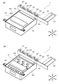
- FIG. 1A is a perspective view of the film capacitor according to the embodiment
- FIG. 1B is a perspective view of the film capacitor according to the embodiment before the filling resin is filled in the case.
- FIG. 2 is an exploded perspective view of the capacitor element unit according to the embodiment.
- 3A and 3B are perspective views of the first bus bar as viewed from the front upper side and the rear lower side, respectively, according to the embodiment.
- 4 (a) and 4 (b) are perspective views of the second bus bar as viewed from the front upper side and the rear lower side, respectively, according to the embodiment.
- FIG. 5 is a perspective view of the case according to the embodiment.
- FIG. 6 is a side sectional view of the film capacitor cut at the position of the support rib on the right side of the case according to the embodiment.
- 7 (a) and 7 (b) are a plan view and a side view of the capacitor element unit according to the modified example, respectively.
- the film capacitor 1 which is an embodiment of the capacitor of the present invention, will be described with reference to the drawings.
- each figure is appropriately marked with front-back, left-right, and up-down directions.
- the direction shown is only a relative direction of the film capacitor 1 and does not indicate an absolute direction.
- names may be given according to the directions shown in the drawings.
- the film capacitor 1 corresponds to the “capacitor” described in the claims.
- the first end face electrode 110 and the second end face electrode 120 correspond to the “electrode” described in the claims.
- the first bus bar 200 corresponds to the "bus bar” described in the claims
- the second bus bar 300 corresponds to the "other bus bar” described in the claims.
- FIG. 1A is a perspective view of the film capacitor 1
- FIG. 1B is a perspective view of the film capacitor 1 before the filling resin 500 is filled in the case 400.
- the film capacitor 1 includes six capacitor elements 100, a first bus bar 200, a second bus bar 300, a case 400, and a filling resin 500.
- the condenser element unit 10 is configured by assembling the six condenser elements 100, the first bus bar 200, and the second bus bar 300 so as to be integrated.
- the capacitor element unit 10 is housed in the case 400, and the filling resin 500 is filled in the case 400.
- the filling resin 500 is a thermosetting resin, for example, an epoxy resin. The portion of the capacitor element unit 10 buried in the filling resin 500 is protected from moisture and impact by the case 400 and the filling resin 500.
- FIG. 2 is an exploded perspective view of the capacitor element unit 10.
- the capacitor element 100 is formed by stacking two metallized films on which aluminum is vapor-deposited on a dielectric film, winding or laminating the laminated metallized films, and pressing them flat.
- the capacitor element 100 has a shape close to a flat long cylinder.
- the first end face electrode 110 is formed on one end face 101 by spraying a metal such as zinc
- the second end face electrode 120 is formed on the other end face 102 by spraying a metal such as zinc. It is formed.
- the six capacitor elements 100 are arranged in two rows in the front-rear direction and three in each row in a state where both end faces 101 and 102 face in the vertical direction. 2 Bus bars 300 are connected.
- the capacitor element 100 of the present embodiment is formed of a metallized film in which aluminum is vapor-deposited on a dielectric film, but in addition to this, metallization in which other metals such as zinc and magnesium are vapor-deposited. It may be formed of a film. Alternatively, the capacitor element 100 may be formed of a metallized film obtained by depositing a plurality of metals among these metals, or may be formed of a metallized film obtained by depositing an alloy of these metals. ..
- 3 (a) and 3 (b) are perspective views of the first bus bar 200 as viewed from the front upper side and the rear lower side, respectively.
- the first bus bar 200 is formed by appropriately cutting out and bending a conductive material, for example, a copper plate, and has an electrode terminal portion 210, three first connection terminal portions 220, a second connection terminal portion 230, and a relay terminal portion. It has a configuration in which the 240 and the two support portions 250 are integrated. In the present embodiment, the first bus bar 200 is an N-pole bus bar.
- the electrode terminal portion 210 has a rectangular shape when viewed from above, and covers the first end surface electrodes 110 of the six capacitor elements 100 from above.
- the electrode terminal portion 210 has an elongated rectangular front plate portion 211, a rectangular rear plate portion 212, and an overhanging portion 213 that projects upward in a rectangular wave shape between the front plate portion 211 and the rear plate portion 212. It is composed of and.
- the upper surface of the overhanging portion 213 is formed on a flat surface 213a.
- connection pins 214 are formed on the front plate portion 211 at the front end portion so as to be arranged in the left-right direction. Further, the rear plate portion 212 is formed with six openings 215 arranged in two rows in the front-rear direction and slightly offset in the front-rear direction in the left-right direction, and connection pins 214 are formed at the trailing edge of each opening 215.
- connection pins 214 of the front plate portion 211 come into contact with the first end surface electrode 110 of each capacitor element 100 in the front row, and 2 of the rear plate portion 212 with respect to the first end surface electrode 110 of each capacitor element 100 in the rear row.
- the two connecting pins 214 come into contact.
- Each connection pin 214 is joined to the corresponding first end face electrode 110 by a joining method such as soldering.
- the first bus bar 200 is electrically connected to the first end face electrode 110 of the six capacitor elements 100. Since the thickness of each connection pin 214 is smaller than the thickness of other portions of the electrode terminal portion 210, heat is less likely to be absorbed by the connection pin 214, and soldering or the like is facilitated.
- the relay terminal unit 240 relays between the electrode terminal unit 210 and the three first connection terminal units 220 and the second connection terminal unit 230.
- the relay terminal portion 240 rises from the lower plate portion 241 that extends upward from the rear end portion of the electrode terminal portion 210 and then bends and extends rearward, and the rear end portion of the lower plate portion 241 and rises from the lower plate portion 241.
- the three first connection terminal portions 220 are provided at the upper end portions of the upper plate portion 242 of the relay terminal portion 240 so as to be arranged in the left-right direction at equal intervals.
- the first connection terminal portion 220 has a hook shape that extends upward and then bends and extends rearward.
- a circular through hole 221 is formed in the first connection terminal portion 220.
- a nut 222 is fitted into the through hole 221.
- the second connection terminal portion 230 is provided at the right end of the upper end portion of the upper plate portion 242 of the relay terminal portion 240.
- the second connection terminal portion 230 has a shape that extends slightly upward and then bends and extends long rearward.
- a circular through hole 231 is formed at the tip of the second connection terminal portion 230.
- Each of the two support portions 250 is provided so as to hang down from the left and right ends of the rear plate portion 212 of the electrode terminal portion 210, and has an elongated rectangular shape.
- the support portion 250 is formed with inverted U-shaped fitting ports 251 at two locations at the lower end portion.
- 4 (a) and 4 (b) are perspective views of the second bus bar 300 as viewed from the front upper side and the rear lower side, respectively.
- the second bus bar 300 is formed by appropriately cutting out and bending a conductive material, for example, a copper plate, and has an electrode terminal portion 310, three first connection terminal portions 320, a second connection terminal portion 330, and a relay terminal portion. It has a structure in which the 340 is integrated. In the present embodiment, the second bus bar 300 is a P-pole bus bar.
- the electrode terminal portion 310 has a rectangular shape and covers the second end face electrode 120 of the six capacitor elements 100 from below.
- Six connection pins 311 are formed at the front end of the electrode terminal 310 so as to be arranged in the left-right direction.
- the electrode terminal portion 310 is formed with six openings 312 arranged in two rows in the front-rear direction so as to be displaced in the front-rear direction in the left-right direction, and connection pins 311 are formed at the trailing edge of each opening 312.
- the electrode terminal portion 310 is provided with two circular flow holes 313 in front of the six openings 312.
- connection pins 311 of the electrode terminal portion 310 come into contact with the second end face electrode 120 of each capacitor element 100.
- Each connection pin 311 is joined to the corresponding second end face electrode 120 by a joining method such as soldering.
- the second bus bar 300 is electrically connected to the second end face electrode 120 of the six capacitor elements 100. Since the thickness of each connection pin 311 is smaller than the thickness of the other portion of the electrode terminal portion 310, heat is less likely to be absorbed by the connection pin 311 and soldering or the like is facilitated.
- the relay terminal unit 340 relays between the electrode terminal unit 310 and the three first connection terminal units 320 and the second connection terminal unit 330.
- the relay terminal portion 340 extends upward from the rear end portion of the electrode terminal portion 310, and the upper end portion thereof extends upward from the lower plate portion 341 and the upper end portion of the lower plate portion 341 that slightly protrudes forward, and the lower plate portion 340 extends upward. It is composed of an upper plate portion 342 that overhangs to the right side of the portion 341.
- Six oval flow holes 343 are formed in the lower plate portion 341 so as to be arranged in the left-right direction.
- the three first connection terminal portions 320 are provided at the upper end portions of the upper plate portion 342 of the relay terminal portion 340 so as to be arranged in the left-right direction at equal intervals.
- the first connection terminal portion 320 has a hook shape that extends upward and then bends and extends rearward.
- a circular through hole 321 is formed in the first connection terminal portion 320.
- a nut 322 is fitted into the through hole 321.
- the second connection terminal portion 330 is provided at the right end of the upper end portion of the upper plate portion 342 of the relay terminal portion 340.
- the second connection terminal portion 330 has a shape that extends slightly upward and then bends and extends long rearward.
- a circular through hole 331 is formed at the tip of the second connection terminal portion 330.
- the relay terminal portion 240 of the first bus bar 200 the upper surface of the lower plate portion 241 and the front and rear surfaces of the upper plate portion 242 are covered with the first insulating sheet 600. Further, in the relay terminal portion 340 of the second bus bar 300, the upper front and rear surfaces of the lower plate portion 341 and the front and rear surfaces of the upper plate portion 342 are covered with the second insulating sheet 700.
- the first insulating sheet 600 and the second insulating sheet 700 are formed of an insulating paper or a resin material having electrical insulating properties such as acrylic and silicon.
- the first insulating sheet 600 and the second insulating sheet 700 provide an insulation distance between the first bus bar 200 and the second bus bar 300, an insulation distance between the second bus bar 300 and the first end face electrode 110 of the capacitor element 100, and the like. Secured.
- the three first connection terminal portions 220 of the first bus bar 200 and the three first connection terminal portions 320 of the second bus bar 300 are arranged alternately in the left-right direction, and the first bus bar 200
- the second connection terminal portion 230 and the second connection terminal portion 330 of the second bus bar 300 are arranged in the left-right direction.
- FIG. 5 is a perspective view of the case 400.
- the case 400 is made of resin and is formed of, for example, polyphenylene sulfide (PPS) which is a thermoplastic resin.
- PPS polyphenylene sulfide
- the case 400 is formed in a box shape having a substantially rectangular parallelepiped shape, and has a bottom surface portion 401, a front side surface portion 402 rising from the bottom surface portion 401, a rear side surface portion 403, a left side surface portion 404, and a right side surface portion 405, and the upper surface is open.
- a mounting tab 410 is provided at the upper end of the front ends of the left side surface portion 404 and the right side surface portion 405.
- a mounting hole 411 is formed in the mounting tab 410.
- These mounting tabs 410 are used when the film capacitor 1 is fixed to the installation portion of an external device such as an inverter device.
- support ribs 420 extending upward from the bottom surface portion 401 are formed at two front and rear positions on the inner wall surface. The distance between the front and rear support ribs 420 is equal to the distance between the front and rear fitting ports 251 of the support portion 250 of the first bus bar 200.
- the capacitor element unit 10 is housed in the case 400.
- the tip ends of the left and right support ribs 420 of the case 400 are fitted into the fitting ports 251 of the left and right support portions 250 of the first bus bar 200.
- the capacitor element unit 10 is positioned in the front-rear, left-right, and up-down directions with respect to the case 400.
- one end face 101 that is, the first end face electrode 110 faces the opening 400a side of the case 400
- the other end face 102 that is, the second end face electrode 120 faces the bottom surface portion 401 side of the case 400.
- the filled resin 500 in the liquid phase state is injected into the case 400.
- the filling resin 500 passes through the flow holes 313 and 343 of the second bus bar 300, the filling resin 500 is easily distributed between the capacitor element unit 10 and the bottom surface portion 401 of the case 400.
- the case 400 is heated. As a result, the filling resin 500 in the case 400 is cured.
- the film capacitor 1 is completed as shown in FIG. 1 (a).
- FIG. 6 is a side sectional view of the film capacitor 1 cut at the position of the support rib 420 on the right side of the case 400.
- the filling resin 500 in the case 400 is in a state in which only the casting surface (the surface exposed to the outside) is drawn with a solid line.
- the first bus bar 200 is exposed from the filling resin 500 in the case 400, and the first portion 201 (enclosed by a two-dot chain line) provided with the first connection terminal portion 220 and the second connection terminal portion 230. ), A buried portion 202a (enclosed by a broken line) buried in the filling resin 500, and an exposed portion 202b (enclosed by a alternate long and short dash line) exposed from the filling resin 500. Includes a second portion 202, which is provided with. The exposed portion 202b is located away from the first portion 201, that is, separated from the first portion 201 by the rear buried portion 202a.
- the six capacitor elements 100 include a capacitor element 100 in the back row close to the first portion 201 and a capacitor element 100 in the front row far from the first portion 201 in the front-rear direction.
- the exposed portion 202b is provided in the second portion 202 so that almost the entire exposed portion 202b rests on the capacitor element 100 in the front row (overlaps when viewed from above) in the front-rear direction.
- the film capacitor 1 can be mounted on, for example, an inverter device for driving an electric motor in an electric vehicle.
- DC power is supplied to the Invar device from the power supply device (battery).
- the inverter device includes an inverter circuit including an IGBT (Insulated Gate Bipolar transistor), converts DC power into three-phase AC power, and supplies it to an electric motor.
- External terminals (not shown) connected to the power supply device correspond to the second connection terminal portion 230 of the first bus bar 200 and the second connection terminal portion 330 of the second bus bar 300, respectively, and use through holes 231 and 331. It is connected by screwing.
- the three first connection terminal portions 220 of the first bus bar 200 and the three first connection terminal portions 320 of the second bus bar 300 have external terminals (not shown) connected to the inverter circuit corresponding to each. It is connected by screwing with nuts 222 and 222.
- the six capacitor elements 100, the first bus bar 200, and the second bus bar 300 When the film capacitor 1 is energized, the six capacitor elements 100, the first bus bar 200, and the second bus bar 300 generate heat due to the current flowing through them.
- the generated heat is applied to the first portion 201 exposed from the filling resin 500 in the first bus bar 200, the upper plate portion 342 of the relay terminal portion 340 exposed from the filling resin 500 in the second bus bar 300, and the first connection terminal portion. It is discharged to the outside from the 320 and the second connection terminal portion 330. Further, in the present embodiment, the generated heat is released to the outside not only from the above portion but also from the exposed portion 202b provided on the first bus bar 200.
- the heat generated by the capacitor element 100 in the front row far from the first portion 201 of the first bus bar 200 is not easily released from the first portion 201.
- the exposed portion 202b is provided so as to be applied to the capacitor element 100 in the front row, the heat of the capacitor element 100 in the front row is also satisfactorily released by the exposed portion 202b.
- the upper surface of the overhanging portion 213, which is the upper surface of the exposed portion 202b, is formed on a flat surface 213a, and when the film condenser 1 is mounted on the inverter device, a cooler prepared on the inverter device side (shown in the figure). Can be mounted on the flat surface 213a. In this case, the heat radiation effect from the exposed portion 202b is further enhanced by being cooled (endothermic) by the cooler.
- the first bus bar 200 connected to the first end surface electrode 110 of the capacitor element 100 is exposed from the filling resin 500, and the first connection terminal portion 220 and the second connection terminal portion 230 are connected to the external terminals.
- the first end surface electrode 110 has a first portion 201, a buried portion 202a buried in the filling resin 500, and an exposed portion 202b located away from the first portion 201 and exposed from the filling resin 500. It is configured to include a second portion 202 provided with a connection pin 214 to be connected.
- the heat generated in the capacitor element 100 and the first bus bar 200 when energized can be discharged to the outside not only from the first portion 201 of the first bus bar 200 but also from the exposed portion 202b. Therefore, since the heat dissipation effect is enhanced, the entire film capacitor 1 is less likely to overheat when energized.
- the capacitor element 100 is housed in the case 400 so that one end surface 101 faces the opening 400a side of the case 400 and the other end surface 102 faces the bottom surface 401 side of the case 400.
- the first bus bar 200 is connected to the first end face electrode 110 of one end face 101
- the second bus bar 300 is connected to the second end face electrode 120 of the other end face 102.
- the second portion 202 of the first bus bar 200 includes a portion facing one end surface 101 (in the embodiment, an electrode terminal portion 210), and a part of the facing portion serves as an overhanging portion 213.
- the exposed portion 202b is formed by projecting in the direction away from the end face 101 (upward).
- the exposed portion 202b can be easily formed on the first bus bar 200. Moreover, since it is not necessary to form a gap for the purpose of insulation or the like between the portion of the first bus bar 200 where the exposed portion 202b is formed and the capacitor element 100, the exposed portion 202b is provided close to the capacitor element 100. be able to. As a result, the heat generated by the capacitor element 100 is easily transferred to the exposed portion 202b, and heat is easily dissipated by the exposed portion 202b.
- the first bus bar 200 has an opening.
- the exposed portion 202b is provided on the portion of the capacitor element 100 facing the 400a side facing the peripheral surface. In this case, it may be necessary to form a gap for the purpose of insulation or the like between the facing portion and the peripheral surface of the capacitor element 100. Therefore, it becomes difficult to provide the exposed portion 202b close to the capacitor element 100.
- a plurality of capacitor elements 100 are arranged side by side in the case 400.
- the plurality of capacitor elements 100 include a capacitor element 100 close to the first portion 201 and a capacitor element 100 far from the first portion 201 in the front-rear direction, and at least a part of the exposed portion 202b is the first portion in the front-rear direction. It is provided in the second portion 202 so as to cover the capacitor element 100 far from 201.
- the heat of the capacitor element 100 far from the first portion 201 can also be satisfactorily released by the exposed portion 202b.
- the exposed portion 202b is configured to have a flat surface 213a.
- the cooler prepared on the external device side can be mounted on the flat surface 213a, and the heat dissipation effect from the exposed portion 202b is further enhanced.
- the capacitor element unit 10 when the number of capacitor elements 100 is increased in the direction in which the distance from the first connection terminal portion 220 and the second connection terminal portion 230, that is, the first portion 201 changes (front-back direction), By increasing the number of overhanging portions 213 accordingly, the number of exposed portions 202b may be increased.
- 7 (a) and 7 (b) are a plan view and a side view of the capacitor element unit 10 according to the modified example, respectively.
- the capacitor element unit 10 includes nine capacitor elements 100 arranged in three rows in the front-rear direction.
- the first bus bar 200 two overhanging portions 213 are provided at the electrode terminal portion 210, and an intermediate plate portion 216 is provided between the two overhanging portions 213.
- Six openings 217 are formed in the intermediate plate portion 216 in the left-right direction, and connection pins 214 are formed at the trailing edge of each opening 217.
- These connection pins 214 are joined to the first end surface electrodes 110 of the three capacitor elements 100 in the second row from the front by a joining method such as soldering.
- the portion of the two overhanging portions 213 that is exposed from the filling resin 500 is the exposed portion 202b.
- the exposed portion 202b on the front side is substantially entirely covered with the capacitor element 100 in the front row, and the exposed portion 202b on the rear side is substantially entirely covered with the capacitor element 100 in the second row from the front.
- the second bus bar 300 is also provided with a connection pin 311 bonded to the second end face electrode 120 of the three capacitor elements 100 in the second row at the electrode terminal portion 310.
- the heat generated by the capacitor element 100 in the front row and the capacitor element 100 in the second row from the front is satisfactorily released to the outside by the exposed portions 202b on the front side and the rear side.
- a plurality of capacitor elements 100 are arranged in a direction (left-right direction) in which the distance from the first portion 201 does not change.
- a configuration in which one capacitor element 100 is arranged in the above direction may be adopted. That is, the film capacitor 1 in which the plurality of capacitor elements 100 are arranged only in the direction in which the distance from the first portion 201 changes (front-back direction) may be configured such that the exposed portion 202b is provided.
- the capacitor elements 100 are arranged so that the longitudinal direction of the capacitor element 100 is the direction in which the distance from the first portion 201 of the first bus bar 200 changes (front-back direction).
- the capacitor elements 100 may be arranged so that the lateral direction of the capacitor element 100 is the direction in which the distance from the first portion 201 of the first bus bar 200 changes (left-right direction).
- almost the entire exposed portion 202b rests on the capacitor element 100 far from the first portion 201 of the first bus bar 200.
- first bus bar 200 and the second bus bar 300 are provided with three first connection terminal portions 220 and 320, but the number of the first connection terminal portions 220 and 320 may be appropriately increased. May be changed.
- first bus bar 200 includes the first portion 201 and the second portion 202 including the exposed portion 202b.
- second bus bar 300 may also be provided with a first portion and a second portion including an exposed portion.
- the first bus bar 200 is an N-pole bus bar
- the second bus bar 300 is a P-pole bus bar
- the first bus bar 200 may be a P-pole bus bar
- the second bus bar 300 may be an N-pole bus bar.
- the capacitor element 100 is formed by stacking two metallized films on which aluminum is vapor-deposited on a dielectric film, and winding or laminating the laminated metallized films.
- these capacitor elements 100 may be formed by laminating a metallized film in which aluminum is vapor-deposited on both sides of a dielectric film and an insulating film, and winding or laminating them.
- the film capacitor 1 was mentioned as an example of the capacitor of the present invention.
- the present invention can also be applied to capacitors other than the film capacitor 1.
- the present invention is useful for capacitors used in various electronic devices, electrical devices, industrial devices, electrical components of vehicles, and the like.
Landscapes
- Engineering & Computer Science (AREA)
- Power Engineering (AREA)
- Microelectronics & Electronic Packaging (AREA)
- Manufacturing & Machinery (AREA)
- Fixed Capacitors And Capacitor Manufacturing Machines (AREA)
Priority Applications (5)
| Application Number | Priority Date | Filing Date | Title |
|---|---|---|---|
| CN202080034687.4A CN113811965B (zh) | 2019-05-24 | 2020-04-27 | 电容器 |
| JP2021522723A JP7390531B2 (ja) | 2019-05-24 | 2020-04-27 | コンデンサ |
| DE112020002551.9T DE112020002551T5 (de) | 2019-05-24 | 2020-04-27 | Kondensator |
| CN202411574165.XA CN119092298A (zh) | 2019-05-24 | 2020-04-27 | 电容器 |
| US17/485,309 US11776758B2 (en) | 2019-05-24 | 2021-09-24 | Capacitor |
Applications Claiming Priority (2)
| Application Number | Priority Date | Filing Date | Title |
|---|---|---|---|
| JP2019097692 | 2019-05-24 | ||
| JP2019-097692 | 2019-05-24 |
Related Child Applications (1)
| Application Number | Title | Priority Date | Filing Date |
|---|---|---|---|
| US17/485,309 Continuation US11776758B2 (en) | 2019-05-24 | 2021-09-24 | Capacitor |
Publications (1)
| Publication Number | Publication Date |
|---|---|
| WO2020241145A1 true WO2020241145A1 (ja) | 2020-12-03 |
Family
ID=73554034
Family Applications (1)
| Application Number | Title | Priority Date | Filing Date |
|---|---|---|---|
| PCT/JP2020/017889 Ceased WO2020241145A1 (ja) | 2019-05-24 | 2020-04-27 | コンデンサ |
Country Status (5)
| Country | Link |
|---|---|
| US (1) | US11776758B2 (https=) |
| JP (1) | JP7390531B2 (https=) |
| CN (2) | CN119092298A (https=) |
| DE (1) | DE112020002551T5 (https=) |
| WO (1) | WO2020241145A1 (https=) |
Cited By (4)
| Publication number | Priority date | Publication date | Assignee | Title |
|---|---|---|---|---|
| JP2020031139A (ja) * | 2018-08-22 | 2020-02-27 | 株式会社指月電機製作所 | コンデンサ |
| WO2022117327A1 (de) * | 2020-12-04 | 2022-06-09 | Robert Bosch Gmbh | Baugruppe umfassend einen kondensator, insbesondere einen zwischenkreiskondensator für ein mehrphasensystem und verbesserte wärmeabfuhr an polen stromschienen anschluss |
| JP2022119028A (ja) * | 2021-02-03 | 2022-08-16 | 株式会社指月電機製作所 | コンデンサ |
| WO2024004754A1 (ja) | 2022-06-29 | 2024-01-04 | ニチコン株式会社 | コンデンサ |
Families Citing this family (2)
| Publication number | Priority date | Publication date | Assignee | Title |
|---|---|---|---|---|
| JP7180625B2 (ja) | 2020-02-03 | 2022-11-30 | 株式会社デンソー | 電力変換装置 |
| DE102023201394A1 (de) * | 2023-02-17 | 2024-08-22 | Robert Bosch Gesellschaft mit beschränkter Haftung | Kondensator, insbesondere Zwischenkreiskondensator für ein Mehrphasensystem |
Citations (4)
| Publication number | Priority date | Publication date | Assignee | Title |
|---|---|---|---|---|
| WO2010004704A1 (ja) * | 2008-07-10 | 2010-01-14 | パナソニック株式会社 | モールド型コンデンサとその製造方法 |
| JP2011091250A (ja) * | 2009-10-23 | 2011-05-06 | Denso Corp | コンデンサ及び電力変換装置 |
| WO2016084180A1 (ja) * | 2014-11-27 | 2016-06-02 | 三菱電機株式会社 | 半導体モジュールおよび半導体駆動装置 |
| WO2016103918A1 (ja) * | 2014-12-26 | 2016-06-30 | 株式会社村田製作所 | コンデンサモジュールおよび電力変換システム |
Family Cites Families (5)
| Publication number | Priority date | Publication date | Assignee | Title |
|---|---|---|---|---|
| DE102005018172A1 (de) * | 2005-04-19 | 2006-10-26 | Conti Temic Microelectronic Gmbh | Leistungskondensator |
| WO2014091696A1 (ja) * | 2012-12-10 | 2014-06-19 | パナソニック株式会社 | ケースモールド型コンデンサとその製造方法 |
| DE112015002505B4 (de) * | 2014-05-28 | 2025-11-20 | Panasonic Intellectual Property Management Co., Ltd. | Folienkondensator |
| CN108352252B (zh) * | 2015-11-10 | 2020-03-24 | 松下知识产权经营株式会社 | 薄膜电容器 |
| WO2018170872A1 (en) * | 2017-03-24 | 2018-09-27 | Valeo Siemens Eautomotive Shenzhen Co., Ltd | A capacitor module for use in an inverter |
-
2020
- 2020-04-27 JP JP2021522723A patent/JP7390531B2/ja active Active
- 2020-04-27 WO PCT/JP2020/017889 patent/WO2020241145A1/ja not_active Ceased
- 2020-04-27 CN CN202411574165.XA patent/CN119092298A/zh active Pending
- 2020-04-27 CN CN202080034687.4A patent/CN113811965B/zh active Active
- 2020-04-27 DE DE112020002551.9T patent/DE112020002551T5/de active Pending
-
2021
- 2021-09-24 US US17/485,309 patent/US11776758B2/en active Active
Patent Citations (4)
| Publication number | Priority date | Publication date | Assignee | Title |
|---|---|---|---|---|
| WO2010004704A1 (ja) * | 2008-07-10 | 2010-01-14 | パナソニック株式会社 | モールド型コンデンサとその製造方法 |
| JP2011091250A (ja) * | 2009-10-23 | 2011-05-06 | Denso Corp | コンデンサ及び電力変換装置 |
| WO2016084180A1 (ja) * | 2014-11-27 | 2016-06-02 | 三菱電機株式会社 | 半導体モジュールおよび半導体駆動装置 |
| WO2016103918A1 (ja) * | 2014-12-26 | 2016-06-30 | 株式会社村田製作所 | コンデンサモジュールおよび電力変換システム |
Cited By (8)
| Publication number | Priority date | Publication date | Assignee | Title |
|---|---|---|---|---|
| JP2020031139A (ja) * | 2018-08-22 | 2020-02-27 | 株式会社指月電機製作所 | コンデンサ |
| JP7284491B2 (ja) | 2018-08-22 | 2023-05-31 | 株式会社指月電機製作所 | コンデンサ |
| WO2022117327A1 (de) * | 2020-12-04 | 2022-06-09 | Robert Bosch Gmbh | Baugruppe umfassend einen kondensator, insbesondere einen zwischenkreiskondensator für ein mehrphasensystem und verbesserte wärmeabfuhr an polen stromschienen anschluss |
| JP2022119028A (ja) * | 2021-02-03 | 2022-08-16 | 株式会社指月電機製作所 | コンデンサ |
| JP7508382B2 (ja) | 2021-02-03 | 2024-07-01 | 株式会社指月電機製作所 | コンデンサ |
| WO2024004754A1 (ja) | 2022-06-29 | 2024-01-04 | ニチコン株式会社 | コンデンサ |
| JP2024004608A (ja) * | 2022-06-29 | 2024-01-17 | ニチコン株式会社 | コンデンサ |
| JP7425834B2 (ja) | 2022-06-29 | 2024-01-31 | ニチコン株式会社 | コンデンサ |
Also Published As
| Publication number | Publication date |
|---|---|
| CN119092298A (zh) | 2024-12-06 |
| JP7390531B2 (ja) | 2023-12-04 |
| US20220013298A1 (en) | 2022-01-13 |
| JPWO2020241145A1 (https=) | 2020-12-03 |
| CN113811965A (zh) | 2021-12-17 |
| US11776758B2 (en) | 2023-10-03 |
| DE112020002551T5 (de) | 2022-02-17 |
| CN113811965B (zh) | 2024-11-26 |
Similar Documents
| Publication | Publication Date | Title |
|---|---|---|
| US11776758B2 (en) | Capacitor | |
| JP7336640B2 (ja) | コンデンサ | |
| JP7122657B2 (ja) | コンデンサ | |
| JP7833674B2 (ja) | コンデンサ | |
| JP4538474B2 (ja) | インバータ装置 | |
| WO2022054729A1 (ja) | コンデンサ | |
| CN112136193B (zh) | 电容器 | |
| WO2021014927A1 (ja) | コンデンサ | |
| CN115039188B (zh) | 电容器 | |
| JP4718840B2 (ja) | コンデンサ装置および車両 | |
| JP6406562B2 (ja) | 蓄電ユニット | |
| JP7821980B2 (ja) | コンデンサ | |
| JP4055643B2 (ja) | インバータ装置 | |
| JP7630107B2 (ja) | コンデンサ | |
| JP7365679B2 (ja) | コンデンサ | |
| JP5982625B2 (ja) | コンデンサおよびこのコンデンサを用いたケースモールド型コンデンサ |
Legal Events
| Date | Code | Title | Description |
|---|---|---|---|
| 121 | Ep: the epo has been informed by wipo that ep was designated in this application |
Ref document number: 20815572 Country of ref document: EP Kind code of ref document: A1 |
|
| ENP | Entry into the national phase |
Ref document number: 2021522723 Country of ref document: JP Kind code of ref document: A |
|
| 122 | Ep: pct application non-entry in european phase |
Ref document number: 20815572 Country of ref document: EP Kind code of ref document: A1 |