WO2020234689A1 - 半導体装置 - Google Patents
半導体装置 Download PDFInfo
- Publication number
- WO2020234689A1 WO2020234689A1 PCT/IB2020/054454 IB2020054454W WO2020234689A1 WO 2020234689 A1 WO2020234689 A1 WO 2020234689A1 IB 2020054454 W IB2020054454 W IB 2020054454W WO 2020234689 A1 WO2020234689 A1 WO 2020234689A1
- Authority
- WO
- WIPO (PCT)
- Prior art keywords
- transistor
- bit line
- oxide
- control circuit
- insulator
- Prior art date
- Legal status (The legal status is an assumption and is not a legal conclusion. Google has not performed a legal analysis and makes no representation as to the accuracy of the status listed.)
- Ceased
Links
Images


Classifications
-
- G—PHYSICS
- G11—INFORMATION STORAGE
- G11C—STATIC STORES
- G11C5/00—Details of stores covered by group G11C11/00
- G11C5/02—Disposition of storage elements, e.g. in the form of a matrix array
- G11C5/025—Geometric lay-out considerations of storage- and peripheral-blocks in a semiconductor storage device
-
- G—PHYSICS
- G11—INFORMATION STORAGE
- G11C—STATIC STORES
- G11C11/00—Digital stores characterised by the use of particular electric or magnetic storage elements; Storage elements therefor
- G11C11/21—Digital stores characterised by the use of particular electric or magnetic storage elements; Storage elements therefor using electric elements
- G11C11/34—Digital stores characterised by the use of particular electric or magnetic storage elements; Storage elements therefor using electric elements using semiconductor devices
- G11C11/40—Digital stores characterised by the use of particular electric or magnetic storage elements; Storage elements therefor using electric elements using semiconductor devices using transistors
- G11C11/401—Digital stores characterised by the use of particular electric or magnetic storage elements; Storage elements therefor using electric elements using semiconductor devices using transistors forming cells needing refreshing or charge regeneration, i.e. dynamic cells
- G11C11/403—Digital stores characterised by the use of particular electric or magnetic storage elements; Storage elements therefor using electric elements using semiconductor devices using transistors forming cells needing refreshing or charge regeneration, i.e. dynamic cells with charge regeneration common to a multiplicity of memory cells, i.e. external refresh
-
- G—PHYSICS
- G11—INFORMATION STORAGE
- G11C—STATIC STORES
- G11C11/00—Digital stores characterised by the use of particular electric or magnetic storage elements; Storage elements therefor
- G11C11/21—Digital stores characterised by the use of particular electric or magnetic storage elements; Storage elements therefor using electric elements
- G11C11/34—Digital stores characterised by the use of particular electric or magnetic storage elements; Storage elements therefor using electric elements using semiconductor devices
- G11C11/40—Digital stores characterised by the use of particular electric or magnetic storage elements; Storage elements therefor using electric elements using semiconductor devices using transistors
- G11C11/401—Digital stores characterised by the use of particular electric or magnetic storage elements; Storage elements therefor using electric elements using semiconductor devices using transistors forming cells needing refreshing or charge regeneration, i.e. dynamic cells
- G11C11/4063—Auxiliary circuits, e.g. for addressing, decoding, driving, writing, sensing or timing
- G11C11/407—Auxiliary circuits, e.g. for addressing, decoding, driving, writing, sensing or timing for memory cells of the field-effect type
- G11C11/409—Read-write [R-W] circuits
- G11C11/4091—Sense or sense/refresh amplifiers, or associated sense circuitry, e.g. for coupled bit-line precharging, equalising or isolating
-
- G—PHYSICS
- G11—INFORMATION STORAGE
- G11C—STATIC STORES
- G11C11/00—Digital stores characterised by the use of particular electric or magnetic storage elements; Storage elements therefor
- G11C11/21—Digital stores characterised by the use of particular electric or magnetic storage elements; Storage elements therefor using electric elements
- G11C11/34—Digital stores characterised by the use of particular electric or magnetic storage elements; Storage elements therefor using electric elements using semiconductor devices
- G11C11/40—Digital stores characterised by the use of particular electric or magnetic storage elements; Storage elements therefor using electric elements using semiconductor devices using transistors
- G11C11/401—Digital stores characterised by the use of particular electric or magnetic storage elements; Storage elements therefor using electric elements using semiconductor devices using transistors forming cells needing refreshing or charge regeneration, i.e. dynamic cells
- G11C11/4063—Auxiliary circuits, e.g. for addressing, decoding, driving, writing, sensing or timing
- G11C11/407—Auxiliary circuits, e.g. for addressing, decoding, driving, writing, sensing or timing for memory cells of the field-effect type
- G11C11/409—Read-write [R-W] circuits
- G11C11/4094—Bit-line management or control circuits
-
- G—PHYSICS
- G11—INFORMATION STORAGE
- G11C—STATIC STORES
- G11C11/00—Digital stores characterised by the use of particular electric or magnetic storage elements; Storage elements therefor
- G11C11/21—Digital stores characterised by the use of particular electric or magnetic storage elements; Storage elements therefor using electric elements
- G11C11/34—Digital stores characterised by the use of particular electric or magnetic storage elements; Storage elements therefor using electric elements using semiconductor devices
- G11C11/40—Digital stores characterised by the use of particular electric or magnetic storage elements; Storage elements therefor using electric elements using semiconductor devices using transistors
- G11C11/401—Digital stores characterised by the use of particular electric or magnetic storage elements; Storage elements therefor using electric elements using semiconductor devices using transistors forming cells needing refreshing or charge regeneration, i.e. dynamic cells
- G11C11/4063—Auxiliary circuits, e.g. for addressing, decoding, driving, writing, sensing or timing
- G11C11/407—Auxiliary circuits, e.g. for addressing, decoding, driving, writing, sensing or timing for memory cells of the field-effect type
- G11C11/409—Read-write [R-W] circuits
- G11C11/4097—Bit-line organisation, e.g. bit-line layout, folded bit lines
-
- G—PHYSICS
- G11—INFORMATION STORAGE
- G11C—STATIC STORES
- G11C5/00—Details of stores covered by group G11C11/00
- G11C5/02—Disposition of storage elements, e.g. in the form of a matrix array
-
- G—PHYSICS
- G11—INFORMATION STORAGE
- G11C—STATIC STORES
- G11C7/00—Arrangements for writing information into, or reading information out from, a digital store
- G11C7/12—Bit line control circuits, e.g. drivers, boosters, pull-up circuits, pull-down circuits, precharging circuits, equalising circuits, for bit lines
-
- G—PHYSICS
- G11—INFORMATION STORAGE
- G11C—STATIC STORES
- G11C7/00—Arrangements for writing information into, or reading information out from, a digital store
- G11C7/18—Bit line organisation; Bit line lay-out
-
- H—ELECTRICITY
- H10—SEMICONDUCTOR DEVICES; ELECTRIC SOLID-STATE DEVICES NOT OTHERWISE PROVIDED FOR
- H10B—ELECTRONIC MEMORY DEVICES
- H10B12/00—Dynamic random access memory [DRAM] devices
-
- H—ELECTRICITY
- H10—SEMICONDUCTOR DEVICES; ELECTRIC SOLID-STATE DEVICES NOT OTHERWISE PROVIDED FOR
- H10B—ELECTRONIC MEMORY DEVICES
- H10B12/00—Dynamic random access memory [DRAM] devices
- H10B12/20—DRAM devices comprising floating-body transistors, e.g. floating-body cells
-
- H—ELECTRICITY
- H10—SEMICONDUCTOR DEVICES; ELECTRIC SOLID-STATE DEVICES NOT OTHERWISE PROVIDED FOR
- H10B—ELECTRONIC MEMORY DEVICES
- H10B12/00—Dynamic random access memory [DRAM] devices
- H10B12/30—DRAM devices comprising one-transistor - one-capacitor [1T-1C] memory cells
- H10B12/31—DRAM devices comprising one-transistor - one-capacitor [1T-1C] memory cells having a storage electrode stacked over the transistor
- H10B12/312—DRAM devices comprising one-transistor - one-capacitor [1T-1C] memory cells having a storage electrode stacked over the transistor with a bit line higher than the capacitor
-
- H—ELECTRICITY
- H10—SEMICONDUCTOR DEVICES; ELECTRIC SOLID-STATE DEVICES NOT OTHERWISE PROVIDED FOR
- H10D—INORGANIC ELECTRIC SEMICONDUCTOR DEVICES
- H10D30/00—Field-effect transistors [FET]
- H10D30/60—Insulated-gate field-effect transistors [IGFET]
- H10D30/67—Thin-film transistors [TFT]
-
- H—ELECTRICITY
- H10—SEMICONDUCTOR DEVICES; ELECTRIC SOLID-STATE DEVICES NOT OTHERWISE PROVIDED FOR
- H10D—INORGANIC ELECTRIC SEMICONDUCTOR DEVICES
- H10D86/00—Integrated devices formed in or on insulating or conducting substrates, e.g. formed in silicon-on-insulator [SOI] substrates or on stainless steel or glass substrates
- H10D86/40—Integrated devices formed in or on insulating or conducting substrates, e.g. formed in silicon-on-insulator [SOI] substrates or on stainless steel or glass substrates characterised by multiple TFTs
- H10D86/421—Integrated devices formed in or on insulating or conducting substrates, e.g. formed in silicon-on-insulator [SOI] substrates or on stainless steel or glass substrates characterised by multiple TFTs having a particular composition, shape or crystalline structure of the active layer
- H10D86/423—Integrated devices formed in or on insulating or conducting substrates, e.g. formed in silicon-on-insulator [SOI] substrates or on stainless steel or glass substrates characterised by multiple TFTs having a particular composition, shape or crystalline structure of the active layer comprising semiconductor materials not belonging to the Group IV, e.g. InGaZnO
-
- H—ELECTRICITY
- H10—SEMICONDUCTOR DEVICES; ELECTRIC SOLID-STATE DEVICES NOT OTHERWISE PROVIDED FOR
- H10D—INORGANIC ELECTRIC SEMICONDUCTOR DEVICES
- H10D86/00—Integrated devices formed in or on insulating or conducting substrates, e.g. formed in silicon-on-insulator [SOI] substrates or on stainless steel or glass substrates
- H10D86/40—Integrated devices formed in or on insulating or conducting substrates, e.g. formed in silicon-on-insulator [SOI] substrates or on stainless steel or glass substrates characterised by multiple TFTs
- H10D86/60—Integrated devices formed in or on insulating or conducting substrates, e.g. formed in silicon-on-insulator [SOI] substrates or on stainless steel or glass substrates characterised by multiple TFTs wherein the TFTs are in active matrices
-
- G—PHYSICS
- G11—INFORMATION STORAGE
- G11C—STATIC STORES
- G11C11/00—Digital stores characterised by the use of particular electric or magnetic storage elements; Storage elements therefor
- G11C11/21—Digital stores characterised by the use of particular electric or magnetic storage elements; Storage elements therefor using electric elements
- G11C11/34—Digital stores characterised by the use of particular electric or magnetic storage elements; Storage elements therefor using electric elements using semiconductor devices
- G11C11/40—Digital stores characterised by the use of particular electric or magnetic storage elements; Storage elements therefor using electric elements using semiconductor devices using transistors
- G11C11/401—Digital stores characterised by the use of particular electric or magnetic storage elements; Storage elements therefor using electric elements using semiconductor devices using transistors forming cells needing refreshing or charge regeneration, i.e. dynamic cells
-
- G—PHYSICS
- G11—INFORMATION STORAGE
- G11C—STATIC STORES
- G11C16/00—Erasable programmable read-only memories
- G11C16/02—Erasable programmable read-only memories electrically programmable
- G11C16/04—Erasable programmable read-only memories electrically programmable using variable threshold transistors, e.g. FAMOS
- G11C16/0466—Erasable programmable read-only memories electrically programmable using variable threshold transistors, e.g. FAMOS comprising cells with charge storage in an insulating layer, e.g. metal-nitride-oxide-silicon [MNOS], silicon-oxide-nitride-oxide-silicon [SONOS]
-
- G—PHYSICS
- G11—INFORMATION STORAGE
- G11C—STATIC STORES
- G11C2207/00—Indexing scheme relating to arrangements for writing information into, or reading information out from, a digital store
- G11C2207/002—Isolation gates, i.e. gates coupling bit lines to the sense amplifier
-
- G—PHYSICS
- G11—INFORMATION STORAGE
- G11C—STATIC STORES
- G11C7/00—Arrangements for writing information into, or reading information out from, a digital store
- G11C7/06—Sense amplifiers; Associated circuits, e.g. timing or triggering circuits
- G11C7/065—Differential amplifiers of latching type
-
- H—ELECTRICITY
- H10—SEMICONDUCTOR DEVICES; ELECTRIC SOLID-STATE DEVICES NOT OTHERWISE PROVIDED FOR
- H10B—ELECTRONIC MEMORY DEVICES
- H10B41/00—Electrically erasable-and-programmable ROM [EEPROM] devices comprising floating gates
- H10B41/70—Electrically erasable-and-programmable ROM [EEPROM] devices comprising floating gates the floating gate being an electrode shared by two or more components
Definitions
- the semiconductor device is a device that utilizes semiconductor characteristics, and refers to a circuit including a semiconductor element (transistor, diode, photodiode, etc.), a device having the same circuit, and the like. It also refers to all devices that can function by utilizing semiconductor characteristics. For example, an integrated circuit, a chip having an integrated circuit, and an electronic component in which the chip is housed in a package are examples of semiconductor devices. Further, the storage device, the display device, the light emitting device, the lighting device, the electronic device, and the like are themselves semiconductor devices, and may have the semiconductor device.
- IGZO In-Ga-Zn oxides
- Exo In-Ga-Zn oxides
- CAAC c-axis aligned crystalline
- nc nanocrystalline structure
- Oxide semiconductor transistor or "OS transistor”
- OS transistor Oxide semiconductor transistor
- Various semiconductor devices using OS transistors have been manufactured (for example, Non-Patent Documents 3 and 4).
- Patent Document 1 discloses a configuration in which a plurality of layers of a memory cell array having an OS transistor are laminated on a substrate provided with a Si transistor.
- one aspect of the present invention is to provide a semiconductor device having a novel configuration or the like, which has excellent reliability of read data in a semiconductor device that functions as a storage device using a minimum off-current.
- one aspect of the present invention is a semiconductor device having a novel configuration capable of writing back data without inverting the logic of the read data in a semiconductor device that functions as a storage device using a minimum off-current. Is one of the issues to be provided.
- One aspect of the present invention is a second control circuit having a first transistor using a silicon substrate as a channel and a second transistor provided on the first control circuit using a metal oxide as a channel.
- the first control circuit has a sense amplifier circuit having an input terminal and an inverted input terminal, and reads data from the memory circuit to the first control circuit.
- the second control circuit is a semiconductor device that controls whether or not to charge the discharged global bit line and the inverted global bit line according to the data read from the memory circuit.
- One aspect of the present invention is a second control circuit having a first transistor using a silicon substrate as a channel and a second transistor provided on the first control circuit using a metal oxide as a channel.
- a plurality of changeover switches provided between the global bit line and the inverted global bit line having the above, and between the global bit line and the second control circuit, and between the inverted global bit line and the second control circuit.
- the first control circuit has a sense amplifier having an input terminal and an inverting input terminal, and in the first period of reading data from the memory circuit to the first control circuit, the second control circuit has a 1-bit line and an inverting input terminal. It has a function to control whether or not the charge precharged in the global bit line is discharged according to the data read from the memory circuit.
- the global bit line, the input terminal, and the inverted global bit line are used.
- the second period in which the changeover switch is switched so that the and inverting input terminals are in a conductive state and the data read from the memory circuit is refreshed, the global bit line and inverting input terminal, and the inverting global bit line and input terminal are used.
- Is Is a semiconductor device that switches the changeover switch so that each becomes conductive.
- One aspect of the present invention is a second control circuit having a first transistor using a silicon substrate as a channel and a second transistor provided on the first control circuit using a metal oxide as a channel.
- the first control circuit includes an amplifier circuit, an output terminal, an inverting output terminal, a first switch, a second switch, a signal inverting circuit, and a global bit line and an inverting global bit line.
- the first switch is provided between the global bit line and the output terminal
- the second switch is provided between the inverting global bit line and the inverting output terminal
- the signal inverting circuit is provided. It has a function of giving an inverted potential of logic data corresponding to the potential of a global bit line and an inverted global bit line to an output terminal and an inverted output terminal electrically connected to an amplifier circuit, and is a first control circuit from a memory circuit.
- the second control circuit In the first period of reading data to, has a function of controlling whether or not the charge precharged in the global bit line and the inverted global bit line is discharged according to the data read from the memory circuit.
- the first switch and the second switch were turned off, and the potential of inverting the logic data according to the potential of the global bit line and the inverted global bit line was electrically connected to the amplifier circuit.
- the second period of refreshing the data read from the memory circuit by giving to the output terminal and the inverting output terminal the output terminal and the inverting output terminal amplified by the amplifier circuit by turning on the first switch and the second switch
- the global bit wire and the inverted global bit wire are preferably semiconductor devices provided in a direction perpendicular to or substantially perpendicular to the surface of the silicon substrate.
- the metal oxide preferably contains a semiconductor device containing In, Ga, and Zn.
- the second control circuit has a fourth transistor to a seventh transistor, and the gate of the fourth transistor has a function of transmitting a signal between the second control circuit and the memory circuit.
- the fifth transistor has the function of controlling the conduction state between the gate of the fourth transistor and either the source or drain of the fourth transistor
- the sixth transistor has a function of controlling the conduction state. It has a function of controlling the conduction state between the other of the source or drain of the 4th transistor and the wiring to which a potential for passing a current flows through the 4th transistor
- the 7th transistor is the 4th transistor.
- a semiconductor device having a function of controlling the conduction state between one of the source or drain of the transistor and the global bit line is preferable.
- One aspect of the present invention can provide a semiconductor device or the like having a novel configuration.
- one aspect of the present invention can provide a semiconductor device having a novel configuration and the like, which can reduce manufacturing costs in a semiconductor device that functions as a storage device using a minimum off-current.
- one aspect of the present invention can provide a semiconductor device having a novel configuration and excellent in low power consumption in a semiconductor device that functions as a storage device utilizing a minimum off-current.
- one aspect of the present invention can provide a semiconductor device having a novel configuration, which can reduce the size of a semiconductor device that functions as a storage device using a minimum off-current.
- one aspect of the present invention can provide a semiconductor device having a novel configuration and the like, which functions as a storage device using a minimum off-current and has excellent reliability of read data.
- one aspect of the present invention is a semiconductor device having a novel configuration capable of writing back data without inverting the logic of the read data in a semiconductor device that functions as a storage device using a minimum off-current. Can be provided.
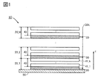
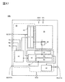
- FIG. 1 is a block diagram showing a configuration example of a semiconductor device.
- 2A and 2B are a block diagram and a circuit diagram showing a configuration example of a semiconductor device.
- 3A and 3B are circuit diagrams showing a configuration example of a semiconductor device.
- FIG. 4 is a circuit diagram showing a configuration example of a semiconductor device.
- FIG. 5 is a circuit diagram showing a configuration example of a semiconductor device.
- FIG. 6 is a circuit diagram showing a configuration example of a semiconductor device.
- FIG. 7 is a circuit diagram showing a configuration example of a semiconductor device.
- FIG. 8 is a circuit diagram showing a configuration example of the semiconductor device.
- FIG. 9 is a circuit diagram showing a configuration example of a semiconductor device.
- FIG. 9 is a circuit diagram showing a configuration example of a semiconductor device.
- FIG. 10 is a timing chart showing a configuration example of the semiconductor device.
- FIG. 11 is a circuit diagram showing a configuration example of a semiconductor device.
- FIG. 12 is a timing chart showing a configuration example of the semiconductor device.
- FIG. 13 is a circuit diagram showing a configuration example of the semiconductor device.
- FIG. 14 is a circuit diagram showing a configuration example of a semiconductor device.
- FIG. 15 is a circuit diagram showing a configuration example of a semiconductor device.
- FIG. 16 is a circuit diagram showing a configuration example of a semiconductor device.
- FIG. 17 is a circuit diagram showing a configuration example of a semiconductor device.
- FIG. 18 is a circuit diagram showing a configuration example of a semiconductor device.
- FIG. 19 is a circuit diagram showing a configuration example of a semiconductor device.
- FIG. 11 is a circuit diagram showing a configuration example of a semiconductor device.
- FIG. 12 is a timing chart showing a configuration example of the semiconductor device.
- FIG. 13 is a
- FIG. 20 is a circuit diagram showing a configuration example of a semiconductor device.
- FIG. 21 is a circuit diagram showing a configuration example of a semiconductor device.
- FIG. 22 is a circuit diagram showing a configuration example of the semiconductor device.
- FIG. 23 is a circuit diagram showing a configuration example of the semiconductor device.
- FIG. 24 is a circuit diagram showing a configuration example of the semiconductor device.
- FIG. 25 is a circuit diagram showing a configuration example of the semiconductor device.
- FIG. 26 is a circuit diagram showing a configuration example of a semiconductor device.
- FIG. 27 is a circuit diagram showing a configuration example of a semiconductor device.
- FIG. 28 is a circuit diagram showing a configuration example of the semiconductor device.
- FIG. 29 is a circuit diagram showing a configuration example of the semiconductor device.
- FIG. 21 is a circuit diagram showing a configuration example of a semiconductor device.
- FIG. 22 is a circuit diagram showing a configuration example of the semiconductor device.
- FIG. 23 is a circuit diagram showing
- FIG. 30 is a circuit diagram showing a configuration example of a semiconductor device.
- FIG. 31 is a circuit diagram showing a configuration example of the semiconductor device.
- FIG. 32 is a circuit diagram showing a configuration example of a semiconductor device.
- FIG. 33 is a circuit diagram showing a configuration example of the semiconductor device.
- 34A and 34B are schematic views showing a configuration example of a semiconductor device.
- FIG. 35 is a schematic view showing a configuration example of a semiconductor device.
- 36A and 36B are circuit diagrams showing a configuration example of a semiconductor device.
- 37A and 37B are a block diagram and a circuit diagram showing a configuration example of a semiconductor device.
- 38A and 38B are block diagrams showing a configuration example of a semiconductor device.
- FIG. 31 is a circuit diagram showing a configuration example of the semiconductor device.
- FIG. 32 is a circuit diagram showing a configuration example of a semiconductor device.
- FIG. 33 is a circuit diagram showing a configuration example of the semiconductor device
- FIG. 39 is a schematic cross-sectional view showing a configuration example of the semiconductor device.
- 40A and 40B are schematic cross-sectional views showing a configuration example of a semiconductor device.
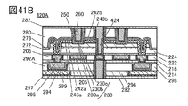
- 41A, 41B, and 41C are schematic cross-sectional views showing a configuration example of a semiconductor device.
- FIG. 42 is a schematic cross-sectional view showing a configuration example of the semiconductor device.
- FIG. 43 is a schematic cross-sectional view showing a configuration example of the semiconductor device.
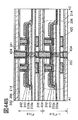
- 44A, 44B, and 44C are a top view and a schematic cross-sectional view showing a configuration example of the semiconductor device.
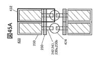
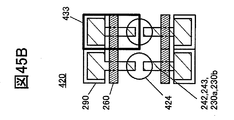
- 45A, 45B, 45C, and 45D are top views for explaining a configuration example of the semiconductor device.
- FIG. 46A is a diagram illustrating classification of the crystal structure of IGZO.
- FIG. 46B is a diagram illustrating an XRD spectrum of a CAAC-IGZO film.
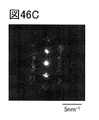
- FIG. 46C is a diagram for explaining the microelectron diffraction pattern of the CAAC-IGZO film.
- FIG. 47 is a block diagram illustrating a configuration example of the semiconductor device.
- FIG. 48 is a conceptual diagram showing a configuration example of a semiconductor device.
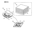
- 49A and 49B are schematic views illustrating an example of an electronic component.
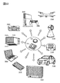
- FIG. 50 is a diagram showing an example of an electronic device.
- the ordinal numbers "1st”, “2nd”, and “3rd” are added to avoid confusion of the components. Therefore, the number of components is not limited. Moreover, the order of the components is not limited. Further, for example, the component referred to in “first” in one of the embodiments of the present specification and the like is referred to as another embodiment or the component referred to in “second” in the scope of the patent claim. It is possible. Further, for example, the component referred to in “first” in one of the embodiments of the present specification and the like may be omitted in another embodiment or in the claims.
- the power supply potential VDD may be abbreviated as potentials VDD, VDD, etc. This also applies to other components (eg, signals, voltages, circuits, elements, electrodes, wiring, etc.).
- the code is used for identification such as "_1”, “_2”, “[n]", “[m, n]”. May be added and described.
- the second wiring GL is described as wiring GL [2].
- a semiconductor device is a device that utilizes semiconductor characteristics, and is a circuit that includes semiconductor elements (transistors, diodes, photodiodes, etc.) and a device that has the same circuit.
- the semiconductor device described in this embodiment can function as a storage device using a transistor having a minimum off-current.
- FIG. 1 is a block diagram for explaining a schematic view of a cross-sectional structure of the semiconductor device 10.
- the semiconductor device 10 has a plurality of element layers 20_1 to 20_M (M is a natural number) on the silicon substrate 50.
- the element layers 20_1 to 20_M have a transistor layer 30 and a transistor layer 40, respectively.
- the transistor layer 40 is composed of a plurality of transistor layers 41_1 to 41_k (k is a natural number of 2 or more).
- the schematic diagram shown in FIG. 1 defines the z-axis direction in order to explain the arrangement of each configuration.
- the z-axis direction refers to a direction perpendicular to the surface of the silicon substrate 50 or a substantially vertical direction.
- the term "approximately vertical" means a state in which the objects are arranged at an angle of 85 degrees or more and 95 degrees or less.
- the z-axis direction may be referred to as the vertical direction.
- the surface of the silicon substrate 50 corresponds to a surface formed on the x-axis and the y-axis defined in the direction perpendicular to the z-axis direction or the substantially vertical direction.
- the x-axis direction may be referred to as the depth direction and the y-axis direction may be referred to as the horizontal direction.
- the transistor layer 40 composed of a plurality of transistor layers 41_1 to 41_k includes a memory circuit having a plurality of memory cells (not shown) in each transistor layer. Each memory cell has a transistor and a capacitor. The capacitor may be called a capacitive element.
- the element layer refers to a layer on which elements such as capacitors and transistors are provided, and is a layer having members such as a conductor, a semiconductor, and an insulator.
- the memory cell of each of the transistor layers 41_1 to 41_k can be called a DOSRAM (Dynamic Oxide Semiconductor Random Access Memory) using a transistor having an oxide semiconductor in the channel forming region (hereinafter referred to as an OS transistor) as the memory. Since it can be configured with one transistor and one capacitance, it is possible to realize a high density of memory. Further, by using the OS transistor, the data retention period can be increased.
- DOSRAM Dynamic Oxide Semiconductor Random Access Memory
- the off current flowing between the source and the drain at the time of off (hereinafter referred to as the off current) is extremely low, which is desired.
- a voltage-dependent charge can be retained in a capacitor on the other side of the source or drain. That is, the data once written can be held in the memory cell for a long time. Therefore, the frequency of data refresh can be reduced and the power consumption can be reduced.
- a memory cell using an OS transistor data can be rewritten and read by charging or discharging electric charges, so that data can be written and read substantially unlimited times.
- a memory cell using an OS transistor is excellent in rewrite resistance because it does not undergo a structural change at the atomic level unlike a magnetic memory or a resistance change type memory.
- a memory cell using an OS transistor does not show instability due to an increase in electron capture centers even in repeated rewriting operations like a flash memory.
- the memory cell using the OS transistor can be freely arranged on a silicon substrate having a transistor having silicon in the channel forming region (hereinafter, Si transistor) or the like, integration can be easily performed. Further, since the OS transistor can be manufactured by using the same manufacturing apparatus as the Si transistor, it can be manufactured at low cost.
- the OS transistor can be a 4-terminal semiconductor element if the back gate electrode is included in addition to the gate electrode, the source electrode and the drain electrode.
- An electric network in which the input and output of signals flowing between the source and the drain can be independently controlled according to the voltage applied to the gate electrode or the back gate electrode can be configured. Therefore, the circuit design can be performed with the same thinking as the LSI.
- OS transistors have better electrical properties than Si transistors in high temperature environments. Specifically, since the ratio of the on-current to the off-current is large even at a high temperature of 125 ° C. or higher and 150 ° C. or lower, good switching operation can be performed.
- the control circuit has a plurality of Si transistors using a silicon substrate 50 as a channel.
- the control circuit included in the silicon substrate 50 includes a sense amplifier circuit composed of Si transistors and the like.
- the control circuit included in the silicon substrate 50 may be referred to as a first control circuit.
- the transistor layer 30 has a function of being able to write and read data to a memory cell selected from one of a plurality of memory cells of the transistor layer 40.
- the transistor layer 30 includes a control circuit having a read-through transistor for reading data and a transistor for controlling data writing and data reading.
- the gate of the read transistor is connected to a local bit line connected to one of a plurality of memory cells. With this configuration, the reading transistor can amplify a slight potential difference of the local bit line and output it to the global bit line when reading data.
- the control circuit provided in the transistor layer 30 has a function as an amplifier circuit composed of OS transistors.
- the control circuit included in the transistor layer 30 may be referred to as a second control circuit.
- the second control circuit may have a function of causing the gate of the reading transistor to hold a potential corresponding to the threshold voltage of the transistor. With this configuration, the reading transistor can reduce the variation in the data read from the memory cell.
- the local bit line LBL is a wiring that is directly connected to the memory cell.
- the global bit line GBL is a wiring that is electrically connected via a second control circuit by selecting any one of a plurality of local bit lines.
- the global bit line GBL or the local bit line LBL has a function of transmitting a signal.
- the data signal given to the global bit line GBL or the local bit line LBL corresponds to a signal written to or read from a memory cell.
- the data signal is described as a binary signal having a high or low level potential corresponding to data 1 or data 0.
- the data signal may be a multi-valued data signal having three or more values.
- the global bit line GBL may function as an inverted global bit line GBLB as a wiring pair for reading data.
- the transistor layer 40 is provided so as to be laminated with the transistor layer 30 in the z-axis direction.
- the transistor layer 40 included in each element layer 20_1 to 20_M is selected by the second control circuit.
- the second control circuit converts the data signal written in the memory cell into a change in the potential of the global bit line GBL by utilizing the difference in the amount of current flowing through the reading transistor of the transistor layer 30. It has a function to output to the control circuit. Further, the second control circuit has a function of giving a data signal output by the first control circuit to the local bit line.
- One embodiment of the present invention uses an OS transistor having an extremely low off-current as a transistor provided in each element layer. Therefore, the frequency of refreshing the data held in the memory cell can be reduced, and the semiconductor device can be made with low power consumption.
- the OS transistors can be stacked and provided, and can be manufactured by repeating the same manufacturing process in the vertical direction, so that the manufacturing cost can be reduced. Further, in one embodiment of the present invention, the transistors constituting the memory cell can be arranged in the vertical direction instead of the plane direction to improve the memory density, and the device can be miniaturized. Further, since the OS transistor has less fluctuation in electrical characteristics than the Si transistor even in a high temperature environment, it can be a semiconductor device that functions as a highly reliable storage device.
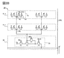
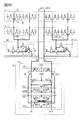
- FIG. 2A shows a block diagram of the element layer 20 corresponding to any one of the element layers 20_1 to 20_M of FIG.
- the element layer 20 has a configuration in which a plurality of transistor layers 40 having memory cells are provided on the transistor layer 30 in the z-axis direction.
- the distance between the transistor layer 30 and the transistor layer 40 can be shortened.
- the parasitic capacitance can be reduced.
- FIG. 2B is a diagram showing each configuration in the element layer 20 shown in FIG. 2A with circuit symbols.
- the transistor layer 30 includes a transistor 31, a transistor 32, a transistor 33, and a control circuit 35 having a transistor 34.
- Each of the transistor layers 41_1 and 41_2 has a plurality of memory cells 42.
- the memory cell 42 has a transistor 43 and a capacitor 44.
- the transistor 43 functions as a switch for switching between a conduction state (on) and a non-conduction state (off) between the local bit line LBL and the capacitor 44 according to the control of the word line WL connected to the gate.
- the local bit line LBL is connected to the gate of the transistor 31.
- the word line WL switches the transistor 43 on or off according to a word signal (sometimes referred to as a signal WL) given to the word line WL.
- a wiring CSL that gives a fixed potential is connected to the capacitor 44.
- Each transistor included in the control circuit 35 is connected as shown in FIG. 2B.
- one of the source and drain of the transistor 33 is connected to the gate of the transistor 31.
- the other of the source or drain of the transistor 33 is connected to one of the source or drain of the transistor 34 and one of the source or drain of the transistor 31.
- One of the source or drain of the transistor 32 is connected to the other of the source or drain of the transistor 31.
- the other of the source or drain of the transistor 32 is connected to the wiring SL.
- the other of the source or drain of the transistor 34 is connected to the global bit line GBL.
- Transistors 32, 33, and 34 function as switches that switch between conductive and non-conducting states between the source and drain, depending on the control of the signals RE, WE, and MUX connected to the gate.
- the signals RE, WE, and MUX are signals for switching on or off of a transistor that functions as a switch, respectively. For example, the signal can be made to function as on at H level and off at L level.
- the transistor 43 is the OS transistor described above. Further, the capacitor 44 has a structure in which an insulator is sandwiched between conductors to be electrodes. As the conductor constituting the electrode, in addition to metal, a semiconductor layer to which conductivity is imparted can be used. The arrangement of the capacitor 44 will be described in detail later, but in addition to the configuration in which the capacitor 44 is arranged at an overlapping position above or below the transistor 43, a part of the semiconductor layer or electrodes constituting the transistor 43 is one electrode of the capacitor 44. Can be used as.
- the transistor 31 has a function of passing a current between the source and drain of the transistor 31 according to the potential of the local bit line LBL. When the potential of the gate of the transistor 31 exceeds the threshold voltage of the transistor 31, a current flows between the source and the drain.
- the control circuit 35 has a function of controlling whether or not a current flowing between the source and drain of the transistor 31 flows between the wiring SL and the global bit line GBL, or the potential of the global bit line GBL is set to the local bit line. It has a function of transmitting to the LBL. Alternatively, it has a function of discharging the potential of the gate of the transistor 31 to the wiring SL via between the source and drain of the transistor 31.
- Transistors 31 to 34 are composed of OS transistors like the transistors 43. Since the transistor layers 30 and 40 constituting the element layer 20 using the OS transistor can be stacked and arranged on the silicon substrate 50 having the Si transistor, integration can be easily performed.
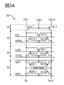
- FIG. 3A shows a circuit configuration example of a control circuit 51 corresponding to a first control circuit composed of Si transistors on a silicon substrate 50.
- the control circuit 51 includes a switch circuit 52, a precharge circuit 53, a precharge circuit 54, a sense amplifier 55, and a global bit line GBL, an inverted global bit line GBLB, a bit line BL, and an inverted bit line BLB connected to the control circuit 51. It is shown in the figure.
- a part of the terminal or wiring connected to the global bit line GBL or the inverted global bit line GBLB in the control circuit 51 may be referred to as an input terminal of the control circuit 51 and an inverting input terminal.
- the bit line BL and the inverting bit line BLB which are the wirings connected to the sense amplifier 55, may be referred to as an output terminal of the control circuit 51 and an inverting output terminal.
- the switch circuit 52 has, for example, n-channel transistors 52_1 and 52_2.
- the transistors 52_1 and 52_2 switch the conduction state between the wiring pair of the global bit line GBL and the inverted global bit line GBLB and the wiring pair of the bit line BL and the inverted bit line BLB according to the signal of the wiring CSEL.
- the switch circuit 52 may be configured to use an analog switch combined with a p-channel type transistor.
- the precharge circuit 53 is composed of n-channel transistors 53_1 to 53_3.
- the precharge circuit 53 is a circuit for precharging the potential VPRE corresponding to the potential VDD / 2 between the bit line BL and the inverting bit line BLB according to the signal of the wiring EQ.
- the precharge circuit 54 is composed of p-channel type transistors 54_1 to 54_3.
- the precharge circuit 54 is a circuit for precharging the potential VPRE corresponding to the potential VDD / 2 between the bit line BL and the inverted bit line BLB according to the signal of the wiring EQB.
- the precharge circuits 53 and 54 may be configured in either one.
- the precharge circuits 53 and 54 have a function of electrically connecting the bit wire BL and the inverting bit wire BLB and balancing (equalizing) them.
- the sense amplifier 55 is composed of p-channel transistors 55_1 and 55_2 and n-channel transistors 55_3 and 55_4 connected to the wiring SAP or the wiring SAN.
- the wiring SAP or wiring SAN is a wiring having a function of giving VDD or VSS.
- Transistors 55_1 to 55_1 are transistors that form an inverter loop.
- FIG. 3B shows a diagram illustrating a circuit block corresponding to the control circuit 51 described with reference to FIG. 3A and the like.
- the control circuit 51 may be represented as a block in drawings and the like.
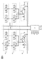
- FIG. 4 is a circuit diagram for explaining an operation example of the semiconductor device 10 of FIG. FIG. 4 is illustrated using the circuit blocks described with reference to FIGS. 3A and 3B.
- the transistor layers 41_1 to 41_k have memory cells 42.
- the memory cell 42 is connected to the paired local bit line LBL and local bit line LBL_pre.
- the memory cell 42 connected to the local bit line LBL is a memory cell into which data is written or read.
- the local bit line LBL_pre is a local bit line that is precharged for potential comparison, and the memory cell connected to the local bit line LBL_pre continues to hold data.
- the local bit line LBL is connected to the global bit line GBL via the control circuit 35.
- the local bit line LBL_pre is electrically connected to the inverted global bit line GBLB via the control circuit 35_pre.
- the global bit line GBL and the inverted global bit line GBLB are electrically connected to the control circuit 51.
- the signals RE, WE, and MUX that control the on / off of the transistors 32, 33, and 34 of the control circuit 35 and the control circuit 35_pre are not shown.
- the signals RE, WE, and MUX are signals that perform different control in the control circuit 35 and the control circuit 35_pre.
- the signals that control the on or off of transistors 32, 33, 34 of the control circuit 35 are the signals RE1, WE1, and MUX1 (not shown), and the on or off of the transistors 32, 33, 34 of the control circuit 35_pre.
- the signals that control the signals are signals RE2, WE2, and MUX2 (not shown).
- FIGS. 5 to 9 show a schematic diagram for explaining the operation of the circuit diagram shown in FIG.
- a part of the wiring electrically connected by turning on or off the transistor functioning as a switch may be shown by a thick line.
- the data held in the memory cell 42 for reading and writing back the data will be described as being the case of holding the data “1”, that is, the potential of the H level (shown as “H” in the figure).
- the transistors of the control circuits 35 and 35_pre, which are turned off, are marked with a cross.
- FIG. 5 is a schematic diagram illustrating a period for precharging the local bit line LBL and the local bit line LBL_pre.
- the transistors 33 and 34 of both the control circuits 35 and 35_pre are turned on, and the precharge voltage V LBL given to the global bit line GBL and the inverted global bit line GBLB is set to the local bit line LBL and the local bit line LBL.
- Precharge is performed by transmitting to the bit line LBL_pre.
- each wiring is boosted to a power supply voltage VDD (eg, 1.5V).
- VDD power supply voltage
- the precharge voltage V LBL corresponds to the potential VPRE described above.
- FIG. 6 is a schematic diagram illustrating a period for holding the threshold voltage VTH of the transistor 31 at the gate of the transistor 31 and correcting the threshold voltage VTH in the read data.
- the control circuit turns off both of the transistors 34 in 35,35_Pre, discharging the precharge voltage V LBL given to the global bit line GBL and the inverted global bit line GBLB wiring SL.
- the voltage of the wiring SL is set to, for example, half of the precharge voltage.
- the potential of the gate of the transistor 31 stops at the threshold voltage of 0.5 ⁇ V LBL + V TH .
- precharging the global bit lines GBL and the inverted global bit line GBLB the voltage V 0.
- the voltage V 0 is a voltage lower than the potential given to other wiring or the like, for example, 0 V.
- the transistor 43 of the memory cell 42 for reading data is turned on, and charge sharing (charge sharing) is performed between the capacitor 44 and the local bit line LBL.
- the potential of the local bit line LBL rises from a voltage of 0.5 ⁇ V LBL + V TH to a voltage of 0.5 ⁇ V LBL + V TH + ⁇ V.
- the voltage ⁇ V referred to here is due to the movement of electric charge due to the H-level potential held in the memory cell 42.
- the transistor 33 is turned off and the potential of the wiring SL is made higher than the voltage V 0 . For example, VDD.
- the voltage at the gate of the transistor 31 rises to a voltage of 0.5 ⁇ V LBL + V TH + ⁇ V due to charge sharing, so that a current I H flows.
- the control circuit 35_pre since the voltage at the gate of the transistor 31 remains at the voltage of 0.5 ⁇ V LBL + V TH , no current flows as compared with the control circuit 35. Therefore, the voltage of the global bit line GBL is higher than the voltage of the inverted global bit line GBLB.
- the transistors 32 and 33 of both the control circuits 35 and 35_pre are turned off, the sense amplifier included in the control circuit 51 is activated, and the voltages of the global bit line GBL and the inverted global bit line GBLB are set to H level or L level. determine.
- the activation of the sense amplifier means an operation of determining the H level or the L level of each wiring according to the voltage difference between the global bit line GBL and the inverted global bit line GBLB.
- the transistors 33 and 34 of both the control circuits 35 and 35_pre and the transistor 43 of the memory cell 42 are turned on, and the voltages of the global bit line GBL and the inverted global bit line GBLB determined in the previous period are applied to the memory cell 42. Write back to.
- the voltage corresponding to the logic of the data read by charge sharing can be written back to the memory cell 42 again without inverting the logic. That is, in the memory cell 42 from which the data “1”, that is, the potential of H level is read, the potential of data “1”, that is, H level can be written back.
- FIG. 10 shows a timing chart for explaining the operation including each period described in FIGS. 5 to 9.
- time T11 to the time T13 correspond to the data writing period.
- Time T13 to time T16 correspond to the threshold voltage acquisition period, that is, the correction period.
- Time T16 to time T18 correspond to a data read period.
- Time T18 to time T20 correspond to a period for writing back data.
- the signals RE, WE, and MUX are different signals in the control circuit 35 and the control circuit 35_pre, but since the control circuit 35 and the control circuit 35_pre perform the same operation, the signals RE, WE, and MUX It is explained as.
- the signal MUX and signal WE are set to H level and the write data is transferred from the sense amplifier, so that one of the wiring pairs of the global bit line GBL or the inverted global bit line GBLB is charged.
- the potential of the local bit line LBL rises.
- the potential of the word line WL is set as the H level, and the potential given to the local bit line LBL (H level in the case of FIG. 10) is written in the memory cell 42.
- the potential of the word line WL is set to the L level. Data is held in the memory cell 42.
- both the wiring SAP and SAN are set to VDD, the signals of the wiring EQ and EQB are inverted, and the wiring pair of the global bit line GBL and the inverted global bit line GBLB are both set to H level.
- the local bit line LBL_pre is precharged to the H level potential.
- the signal MUX is set to L level.
- the signal WE may also be set to L level.
- the signal RE and signal WE are set to H level.
- the potential of the local bit line LBL and the potential of the local bit line LBL_pre are lowered by the discharge via the transistor 31. This discharge stops when the voltage between the gate and the source of the transistor 31 reaches the threshold voltage of the transistor 31.
- both the wiring SAP and SAN are set to VSS (0V), and the wiring pair of the global bit line GBL and the inverted global bit line GBLB is set to the L level.
- both signal WE and signal RE are set to L level.
- the local bit line LBL and the local bit line LBL_pre hold a potential corresponding to the threshold voltage of the transistor 31.
- the wiring EQ and EQB signals are inverted again to stop precharging. That is, the wiring pair of the global bit line GBL and the inverted global bit line GBLB are electrically in a floating state and a floating state. Further, at time T15, the potential of the wiring SL is switched from the L level to the H level. By this switching, the direction of the current flowing through the transistor 31 can be switched.
- the word line WL is set to H level and charge sharing is performed.
- the potential of the local bit line LBL changes according to the data written in the memory cell 42.
- the potential of the local bit line LBL rises, and when the L level data is written to the memory cell 42, the potential of the local bit line LBL falls.
- the local bit line LBL_pre the potential does not change because charge sharing is not performed by the operation of the word line WL.
- the transistor 31 of the control circuit 35 and the transistor 31 of the control circuit 35_pre are set according to the potentials of the local bit line LBL and the local bit line LBL_pre. Current flows. Since the potentials of the local bit line LBL and the local bit line LBL_pre are different, there is a difference in the current flowing between the transistor 31 of the control circuit 35 and the transistor 31 of the control circuit 35_pre. This difference in current depends on the potential of the local bit line LBL that changes due to charge sharing, that is, the data read from the memory cell 42. Therefore, as shown in FIG. 10, the data in the memory cell 42 can be converted into the amount of change in the potential of the wiring pair of the global bit line GBL and the inverted global bit line GBLB.
- the signal RE is set to L level.
- the sense amplifier 55 is operated by applying a power supply voltage (VDD, VSS) to the wiring SAP and SAN.
- VDD, VSS a power supply voltage
- the signal MUX, signal WL, and signal WE are set to L level.
- the writing back of the data according to the logic of the read data is completed.
- the precharge of the local bit line LBL is illustrated for a configuration performed via the global bit line GBL, but the present invention is not limited to this.
- the transistor 37 is provided in the same layer as the control circuit, and the transistor 37 is controlled by the signal PE to perform voltage Vp precharging. With this configuration, it is possible to reduce the power consumption for charging and discharging the global bit line GBL.
- FIG. 12 is a timing chart for explaining the operation in the configuration shown in FIG. 11. As shown in the timing chart shown in FIG. 12, the signal PE is controlled to set the H level from time T13 to time T14. With this configuration, unnecessary charging of the global bit line GBL and the inverted global bit line GBLB can be suppressed.
- the direction of the current flowing through the transistor 31 is changed by switching the potentials of the wiring SL and the global bit line GBL.
- the configuration is inverted. With this configuration, the data written back to the memory cell can be written back without inverting the logic.
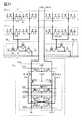
- FIG. 13 is another circuit diagram for explaining an operation example of the semiconductor device 10 of FIG.
- a changeover switch SW for switching the connection between the input terminal of the control circuit 51 and the global bit line GBL and the inverted global bit line GBLB.
- SW_B is provided in the figure.
- the input terminal of the control circuit 51 can switch the connection with the global bit line GBL and the inverted global bit line GBLB by the changeover switches SW and SW_B.
- One of the pair of input terminals of the control circuit 51 may be referred to as a first input terminal and the other may be referred to as a second input terminal.
- the transistor layers 41_1 to 41_k have memory cells 42.
- the memory cell 42 is connected to the paired local bit line LBL and local bit line LBL_pre.
- the memory cell 42 connected to the local bit line LBL is a memory cell into which data is written or read.
- the local bit line LBL_pre is a precharged local bit line, and the memory cell connected to the local bit line LBL_pre continues to hold data.
- the local bit line LBL is connected to the global bit line GBL via the control circuit 35.
- the local bit line LBL_pre is electrically connected to the inverted global bit line GBLB via the control circuit 35_pre.
- the global bit line GBL and the inverted global bit line GBLB are electrically connected to the control circuit 51 via the changeover switch SW or the changeover switch SW_B.
- the signals RE, WE, and MUX that control the on / off of the transistors 32, 33, and 34 of the control circuit 35 and the control circuit 35_pre are not shown.
- the signals RE, WE, and MUX are signals that perform different control in the control circuit 35 and the control circuit 35_pre.
- the signals that control the on or off of the transistors 32, 33, 34 of the control circuit 35 are the signals RE1, WE1, and MUX1, and the signals that control the on or off of the transistors 32, 33, 34 of the control circuit 35_pre are the signals.
- FIGS. 14 to 17 show a schematic diagram for explaining the operation of the circuit diagram shown in FIG.
- a part of the wiring electrically connected by turning on or off the transistor functioning as a switch may be shown by a thick line.
- the data held in the memory cell 42 for reading and writing back the data will be described as being the case of holding the data “1”, that is, the potential of the H level (shown as “H” in the figure).
- the transistors of the control circuits 35 and 35_pre, which are turned off, are marked with a cross.
- the memory data writing is completed, and the voltage is maintained as the initial state by the threshold value correction operation of the local bit line LBL and the local bit line LBL_pre.
- the threshold correction when performing the threshold correction, when the potential of the wiring SL is, for example, half the precharge voltage V LBL , the voltage 0.5 ⁇ V LBL + V TH considering the threshold voltage V TH of the transistor 31. Will be described as a state in which the voltage corresponding to V 1 (for example, VDD) is held in the global bit line GBL and the inverted global bit line GBLB.
- Holding the threshold voltage V TH of the transistor 31 in the local bit lines LBL and the local bit lines LBL_pre is a wiring SL and VSS, it may be performed by discharging the electric charge in the wiring SL via a transistor 31.
- the voltage held in the local bit line LBL and the local bit line LBL_pre is not limited to the threshold voltage and may be another voltage.
- the transistor 43 of the memory cell 42 for reading data is turned on, and charge sharing (charge sharing) is performed between the capacitor 44 and the local bit line LBL.
- the potential of the local bit line LBL rises from a voltage of 0.5 ⁇ V LBL + V TH to a voltage of 0.5 ⁇ V LBL + V TH + ⁇ V.
- the voltage ⁇ V referred to here is due to the movement of electric charge due to the H-level potential held in the memory cell 42.
- the transistor 33 is turned off and the potential of the wiring SL is made lower than the voltage V 0 . For example, VSS (0V).
- the gate voltage rises to a voltage of 0.5 ⁇ V LBL + V TH + ⁇ V due to charge sharing, so that a current I H flows so that the global bit line GBL is discharged.
- the transistor 31 of the control circuit 35_pre since the gate voltage remains the voltage 0.5 ⁇ V LBL + V TH , no current flows as compared with the control circuit 35. Therefore, the voltage of the global bit line GBL drops like a voltage V 1 ⁇ ⁇ V, and the voltage of the inverted global bit line GBLB becomes a voltage V 1 higher than the voltage of the global bit line GBL.
- the first input terminal of the control circuit 51 is connected to either the global bit line GBL or the inverted global bit line GBLB by the changeover switches SW and SW_B.
- the second input terminal of the control circuit 51 is connected to the other of the global bit line GBL or the inverted global bit line GBLB by the changeover switches SW and SW_B.
- transistors 32 and 33 are turned off. Further, in the state of FIG. 15, the first input terminal and the second input terminal of the control circuit 51 are not connected to either the global bit line GBL or the inverted global bit line GBLB by the changeover switches SW and SW_B.
- the global bit wire GBL or the inverted global bit wire GBLB is electrically suspended. This is a first input terminal of the control circuit 51 in a state that voltages V 1 - [Delta] V is maintained, the second input terminal voltages V 1 is maintained.
- the voltage ⁇ V referred to here is due to fluctuations in electric charge due to the current flowing from the global bit line GBL to the wiring SL via the transistor 31.
- the first input terminal and the second input terminal of the control circuit 51 are not connected to either the global bit line GBL or the inverted global bit line GBLB by the changeover switches SW and SW_B.
- the global bit wire GBL or the inverted global bit wire GBLB is electrically suspended.
- the sense amplifier included in the control circuit 51 is activated.
- the first input terminal of the control circuit 51 is connected to the other of the global bit line GBL or the inverted global bit line GBLB by the changeover switches SW and SW_B.
- the second input terminal of the control circuit 51 is connected to either the global bit line GBL or the inverted global bit line GBLB by the changeover switches SW and SW_B. That is, the connection is made in a state different from the state shown in FIG. Then, the global bit line GBL is fixed at the H level, and the inverted global bit line GBLB is fixed at the L level. Then, the transistors 43 of the transistors 33 and 34 and the memory cell 42 are turned on, and the voltages of the determined global bit line GBL and the inverted global bit line GBLB are written back to the memory cell 42.
- the voltage corresponding to the logic of the data read by charge sharing can be written back to the memory cell 42 again without inverting the logic.
- FIGS. 18 to 21 a configuration example different from the description in FIGS. 14 to 17 will be described.
- the transistor 43 of the memory cell 42 for reading data is turned on, and charge sharing (charge sharing) is performed between the capacitor 44 and the local bit line LBL.
- the description in FIG. 18 is the same as the description in FIG.
- the first input terminal of the control circuit 51 is connected to either the global bit line GBL or the inverted global bit line GBLB by the changeover switches SW and SW_B.
- the second input terminal of the control circuit 51 is connected to the other of the global bit line GBL or the inverted global bit line GBLB by the changeover switches SW and SW_B.
- transistors 32 and 33 are turned off. Further, in the state of FIG. 19, the first input terminal and the second input terminal of the control circuit 51 are not connected to either the global bit line GBL or the inverted global bit line GBLB by the changeover switches SW and SW_B.
- the global bit wire GBL or the inverted global bit wire GBLB is electrically suspended. This is a first input terminal of the control circuit 51 in a state that voltages V 1 is held, the second input terminal voltages V 1 - [Delta] V is maintained.
- the first input terminal of the control circuit 51 is connected to the other of the global bit line GBL or the inverted global bit line GBLB by the changeover switches SW and SW_B.
- the second input terminal of the control circuit 51 is connected to either the global bit line GBL or the inverted global bit line GBLB by the changeover switches SW and SW_B. That is, the connection is made in a state different from the state shown in FIG. In this state, the sense amplifier included in the control circuit 51 is activated.
- the global bit line GBL is set to H level
- the inverted global bit line GBLB is set to L level.
- the transistors 43 and 34 and the transistor 43 included in the memory cell 42 are turned on, and the voltages of the determined global bit line GBL and the inverted global bit line GBLB are written back to the memory cell 42.
- the voltage corresponding to the logic of the data read by charge sharing can be written back to the memory cell 42 again without inverting the logic.
- the sense amplifier when the sense amplifier outputs to the outside of the memory, it is output via the bit line BL and the inverted bit line BLB, but the global bit line GBL and the inverted global bit line GBLB. And the logic of the bit line BL and the inverted bit line BLB can be output without becoming the inverted logic.
- FIGS. 22 to 24 a configuration example different from the description in FIGS. 14 to 17 and 18 to 21 will be described.
- the transistor 43 of the memory cell 42 for reading data is turned on, and charge sharing (charge sharing) is performed between the capacitor 44 and the local bit line LBL.
- the description in FIG. 22 is similar to the description in FIG. 14 or FIG.
- the first input terminal of the control circuit 51 is connected to either the global bit line GBL or the inverted global bit line GBLB by the changeover switches SW and SW_B.
- the second input terminal of the control circuit 51 is connected to the other of the global bit line GBL or the inverted global bit line GBLB by the changeover switches SW and SW_B.
- the transistors 32 and 33 are turned off to activate the sense amplifier included in the control circuit 51.
- the global bit line GBL is set to the L level
- the inverted global bit line GBLB is set to the H level.
- the changeover switches SW and SW_B are switched to the side of the first input terminal of the control circuit 51, and the global bit line GBL and the inverted global bit line GBLB are short-circuited. In other words, only the bit line switch to be written back is switched.
- the transistors 43 of the transistors 33 and 34 and the memory cell 42 are turned on, the voltage of the determined global bit line GBL and the inverted global bit line GBLB becomes H, and the data H is written back to the memory cell 42.
- the voltage corresponding to the logic of the data read by charge sharing can be written back to the memory cell 42 again without inverting the logic.
- this drive method only the global bit line GBL to be written back is charged and discharged, so that the energy consumption is half that of switching both the changeover switch SW and SW_B, resulting in low power consumption drive. ..
- the configuration is such that electrons are extracted from the global bit line GBL to the wiring SL, the voltage Vgs between the gate and the source of the transistor 31 can always be kept constant. Therefore, the reading operation can be speeded up.
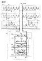
- FIG. 25 is a circuit diagram for explaining an example different from the above-mentioned configuration example 1 and configuration example 2.
- FIG. 25 shows a circuit configuration example of the control circuit 51A corresponding to the first control circuit composed of Si transistors on the silicon substrate 50.
- the control circuit 51A includes a switch circuit 52, a precharge circuit 53, a sense amplifier 55, a potential setting circuit 59, and a global bit line GBL, an inverted global bit line GBLB, a bit line BL, and an inverted bit line BLB connected to the control circuit 51A. It is shown in the figure.
- a part of the terminal or wiring connected to the global bit line GBL or the inverted global bit line GBLB in the control circuit 51A may be referred to as an input terminal of the control circuit 51 and an inverting input terminal.
- the bit line BL and the inverting bit line BLB which are the wirings connected to the sense amplifier 55, may be referred to as an output terminal of the control circuit 51A and an inverting output terminal.
- the switch circuit 52 has, for example, n-channel type transistors 52_1 and 52_2.
- the transistors 52_1 and 52_2 switch the conduction state between the wiring pair of the global bit line GBL and the inverted global bit line GBLB and the wiring pair of the bit line BL and the inverted bit line BLB according to the signal of the wiring CSEL.
- the switch circuit 52 may be configured to use an analog switch combined with a p-channel type transistor.
- the precharge circuit 53 is composed of n-channel type transistors 53_1 to 53_3.
- the precharge circuit 53 is a circuit for balancing and precharging between the bit line BL and the inverting bit line BLB according to the signal of the wiring EQ.
- the potential VPRE corresponds to the potential VDD / 2 between the bit line BL and the inverted bit line BLB.
- the sense amplifier 55 is composed of p-channel transistors 55_1 and 55_2 and n-channel transistors 55_3 and 55_4 connected to the wiring SAP or wiring SAN.
- the wiring SAP or wiring SAN is a wiring having a function of giving VDD or VSS.
- Transistors 55_1 to 55_1 are transistors that form an inverter loop.
- the sense amplifier 55 has a function as a circuit for precharging by applying a precharge voltage to the wiring SAP or the wiring SAN.
- the potential setting circuit 59 has n-channel transistors 57_1 and 57_2 connected to the wiring that gives the potential VSS, and n-channel transistors 58_1 and 58_2 connected to the sense amplifier 55.
- Transistors 57_1 and 57_2 are controlled to be turned on or off according to the signal EN1.
- the current flowing is controlled according to the potentials of the global bit line GBL and the inverted global bit line GBLB connected to the gate.
- the data of the bit line BL and the inverting bit line BLB when the sense amplifier is operated are determined according to the currents flowing through the transistors 58_1 and 58_2.
- FIG. 26 is a circuit diagram for explaining an operation example of the semiconductor device 10 of FIG. FIG. 26 illustrates the configuration of FIG. 2 and the configuration in which the control circuit 51A described with reference to FIG. 25 is applied to the control circuit provided on the silicon substrate 50.
- the transistor layers 41_1 to 41_k have memory cells 42.
- the memory cell 42 is connected to the paired local bit line LBL and local bit line LBL_pre.
- the memory cell 42 connected to the local bit line LBL is a memory cell into which data is written or read.
- the local bit line LBL_pre is a precharged local bit line, and the memory cell connected to the local bit line LBL_pre continues to hold data.
- the local bit line LBL is connected to the global bit line GBL via the control circuit 35.
- the local bit line LBL_pre is electrically connected to the inverted global bit line GBLB via the control circuit 35_pre.
- the global bit wire GBL and the inverted global bit wire GBLB are electrically connected to the control circuit 51A provided on the silicon substrate 50.
- the signals RE, WE, and MUX that control the on / off of the transistor given to the control circuits 35 and 35_pre are different between the control circuit 35 and the control circuit 35_pre, although not shown.
- FIGS. 27 to 33 show a schematic diagram for explaining the operation of the circuit diagram shown in FIG. 26.
- a part of the wiring electrically connected by turning on or off the transistor functioning as a switch may be shown by a thick line.
- the data held in the memory cell 42 for reading and writing back the data will be described as being the case of holding the data “1”, that is, the potential of the H level (shown as “H” in the figure).
- the transistors of the control circuits 35 and 35_pre, which are turned off, are marked with a cross.
- FIG. 27 is a schematic diagram illustrating a period during which the local bit line LBL and the local bit line LBL_pre are precharged.
- the transistors 33 and 34 are turned on and the precharge voltage V LBL given to the global bit line GBL and the inverted global bit line GBLB is transmitted to the local bit line LBL and the local bit line LBL_pre. Precharge.
- FIG. 28 is a schematic diagram illustrating a period for equilibrating (equalizing) the local bit line LBL and the local bit line LBL_pre.
- the transistors 53_1 to 53_3 are turned on to bring the transistor between the global bit line GBL and the inverted global bit line GBLB into a conductive state.
- FIG. 29 is a schematic diagram illustrating a period for holding a voltage reflecting the threshold voltage VTH of the transistor 31 at the gate of the transistor 31 and correcting the threshold voltage VTH in the read data. Is. In this period, the control circuit turns off both of the transistors 34 in 35,35_Pre, discharging the precharge voltage V LBL given to the global bit line GBL and the inverted global bit line GBLB wiring SL. For example, when the potential of the wiring SL is set to half the voltage of the precharge voltage V LBL , the potential of the gate of the transistor 31 stops at the threshold voltage 0.5 ⁇ V LBL + V TH for the current IDis flowing due to the discharge.
- the voltage V 1 is, for example, the potential VPRE.
- the transistors 52_1 and 52_2 are turned off, and the global bit line GBL and the inverted global bit line GBLB (input terminal side), the bit line BL, and the bit line BL and The inverting bit line BLB (output terminal side) is electrically disconnected.
- the global bit line GBL and the inverted global bit line GBLB are electrically suspended.
- the transistor 43 of the memory cell 42 for reading data is turned on, and charge sharing (charge sharing) is performed between the capacitor 44 and the local bit line LBL.
- the potential of the local bit line LBL rises from a voltage of 0.5 ⁇ V LBL + V TH to a voltage of 0.5 ⁇ V LBL + V TH + ⁇ V.
- the voltage ⁇ V is due to the transfer of electric charge due to the H-level potential held in the memory cell 42.
- the control circuit 35,35_Pre turns off the transistor 33, the potential of the wiring SL lower than the precharge voltage V LBL.
- the gate voltage rises to a voltage of 0.5 ⁇ V LBL + V TH + ⁇ V due to charge sharing, so that a current I H flows.
- the transistor 31 of the control circuit 35_pre since the gate voltage remains the voltage 0.5 ⁇ V LBL + V TH , no current flows as compared with the control circuit 35. Therefore, the voltage of the global bit line GBL drops like a voltage V 1 ⁇ ⁇ V, and the voltage of the inverted global bit line GBLB becomes a voltage V 1 .
- the transistors 57_1 and 57_2 are turned on by controlling the signal EN1.
- the transistor 58_1 and the transistor 58_2 there is a difference in the currents I GBL and I GBLB that flow according to the voltage of the global bit line GBL and the inverted global bit line GBLB.
- a potential difference will occur between the bit line BL and the inverted bit line BLB.
- the sense amplifier included in the control circuit 51A is activated by turning off the transistors 57_1 and 57_2 and applying a power supply voltage to the wiring SAP and SAN.
- the bit line BL and the inverted bit line BLB are determined by the logic of H level or L level.
- the logic is an inverted logic of the logic read from the memory cell 42.
- the transistors 43 of the transistors 52_1 and 52_2, the transistors 33 and 34, and the memory cell 42 are turned on, and the voltages of the bit line BL and the inverted bit line BLB determined in the previous period are written back to the memory cell 42.
- the voltage corresponding to the logic of the data read by charge sharing can be written back to the memory cell 42 again without inverting the logic.
- the transistor layer having the memory cell and the control circuit according to one aspect of the present invention has a configuration capable of reading a signal in which the threshold voltage of the transistor for reading data is corrected. With this configuration, the reliability of the data read from the memory cell to the first control circuit can be improved. Further, in the semiconductor device according to one aspect of the present invention, by arranging a plurality of switches between the paired global bit lines, the data can be written back to the memory cell by the logic of the data read from the memory cell.
- FIG. 34A is a perspective view of the semiconductor device 10 in which the element layers 20_1 to 20_M shown in FIG. 1 are arranged on the silicon substrate 50.
- the vertical direction (z-axis direction) in addition to the vertical direction (z-axis direction), the depth direction (x-axis direction) and the horizontal direction (y-axis direction) are shown.
- FIG. 34A the memory cells 42 included in the transistor layers 41_1 and 41_2 are shown by dotted lines.
- the semiconductor device 10 of one aspect of the present invention is provided by stacking transistor layers 30 and 40 having OS transistors. Therefore, it can be manufactured by repeating the same manufacturing process in the vertical direction, and the manufacturing cost can be reduced. Further, in the semiconductor device 10 of one aspect of the present invention, the transistor layers 40 having the memory cells 42 can be stacked and arranged in the vertical direction instead of the plane direction to improve the memory density, and the device can be downsized. Can be planned.
- FIG. 34B illustrates the control logic circuit 61, the row drive circuit 62, the column drive circuit 63, and the output circuit 64, which are composed of Si transistors on the silicon substrate 50.
- the control logic circuit 61, the row drive circuit 62, the column drive circuit 63, and the output circuit 64 will be described in detail in the fourth embodiment.
- FIG. 35 corresponds to a diagram in which the transistor layers 30, 41_1, and 41_2 of the semiconductor device 10 shown in FIG. 34A are extracted and shown.
- FIG. 35 illustrates the transistor 43 and the capacitor 44, the local bit line LBL, and the word line WL included in the memory cells in the transistor layers 41_1 and 41_2.
- the local bit line LBL is shown by a broken line in order to improve visibility.
- FIG. 35 illustrates a global bit line GBL provided so as to penetrate each transistor layer in the z-axis direction. As described above, the global bit line GBL is shown by a thick line as compared with other lines in order to improve visibility.
- the local bit line LBL connected to the transistor 43 of the memory cell, the control circuit 35 of the transistor layer 30, and the global bit line GBL connected to the silicon substrate 50 are z-axis. It is provided in the direction, that is, in the direction perpendicular to the silicon substrate 50.
- the local bit line LBL connected to each memory cell can be shortened. Therefore, since the parasitic capacitance of the local bit line LBL can be significantly reduced, the potential can be read even if the data signal held in the memory cell is made multi-valued. Further, in one aspect of the present invention, since the data held in the memory cell can be read out as a current, the data can be easily read out even if the value is increased.
- each transistor is shown as a transistor having a top gate structure or a bottom gate structure without a back gate electrode, but the structure of the transistor is not limited to this.
- the control circuit 35B may have a back gate electrode connected to the back gate electrode line BGL.
- control circuit 35C may have a back gate electrode connected to the gate electrode.
- the amount of current flowing through each transistor can be increased.
- FIG. 37A shows a block diagram of the semiconductor device 10A corresponding to a modified example of the semiconductor device 10.
- the semiconductor device 10A is different from the semiconductor device 10 in that a transistor layer 90 having a memory cell having a different circuit configuration is provided between the element layer 20 and the transistor layer 30.
- FIG. 37B is a circuit diagram showing a configuration example of the memory cell 91 included in the transistor layer 90.
- the memory cell 91 includes a transistor 92, a transistor 93, and a capacitor 94.
- One of the source and drain of the transistor 92 is connected to the gate of the transistor 93.
- the gate of the transistor 93 is connected to one electrode of the capacitor 94.
- the other of the source or drain of the transistor 92 and one of the source or drain of the transistor 92 are connected to the wiring BL2.
- the other of the source or drain of the transistor 93 is connected to the wiring SL2.
- the other electrode of the capacitor 94 is electrically connected to the wiring CAL.
- a node to which one of the source or drain of the transistor 92, the gate of the transistor 93, and one electrode of the capacitor 94 is connected is referred to as a node N.
- the wiring CAL has a function as wiring for applying a predetermined potential to the other electrode of the capacitor 94.
- the potential of the wiring CAL when reading data from the memory cell 91 is made different from the potential of the wiring CAL when writing data to the memory cell 91 and while holding the data in the memory cell 91.
- the apparent threshold voltage of the transistor 93 when reading data from the memory cell 91 is applied to the apparent threshold voltage of the transistor 93 when writing data to the memory cell 91 and while holding the data in the memory cell 91. It can be different from the threshold voltage of.
- the transistors 92 and 93 are preferably OS transistors.
- the OS transistor has an extremely low off current. Therefore, the charge corresponding to the data written in the memory cell 91 can be held in the node N for a long time. That is, the data once written can be held in the memory cell 91 for a long time. Therefore, the frequency of data refresh can be reduced, and the power consumption of the semiconductor device according to one aspect of the present invention can be reduced.
- the memory cell 91 having the configuration shown in FIG. 37B can be called a NOSRAM (Nonvolatile Oxide Semiconductor RAM) using an OS transistor as a memory.
- NOSRAM has a feature that non-destructive reading can be performed.
- DOSRAM is destructively read when reading the held data.
- the semiconductor device 10A Since the semiconductor device 10A has the memory cell 91, it is possible to transfer data having a high read frequency from the DOS RAM to the NO SRAM. As described above, since the NO SRAM can perform non-destructive reading, the frequency of data refresh can be reduced. Therefore, the power consumption of the semiconductor device according to one aspect of the present invention can be reduced.
- a transistor having one gate is illustrated, but the present invention is not limited to this.
- either one or both of the transistor 92 and the transistor 93 may be a transistor having two gates (a transistor having a front gate and a back gate facing the front gate).
- 38A and 38B show schematic views for explaining a modification of the semiconductor device 10 illustrated in FIG. 1.
- FIG. 38A is a semiconductor device 10B in which the transistor layer 40 is arranged under the transistor layer 30 in the element layers 20_1 to 20_M in the semiconductor device 10 illustrated in FIG. 1.
- the semiconductor device 10B illustrated in FIG. 38A has a transistor layer 49 having transistor layers 49_1 to 49_k in the lower layer of the transistor layer 30. Even in this configuration, it is possible to perform an operation of correcting the threshold voltage of the reading transistor.
- FIG. 38B is a semiconductor device 10C in which the transistor layer 49 described with reference to FIG. 38A is added to the transistor layer 40 in the element layers 20_1 to 20_M of the semiconductor device 10 shown in FIG. Even in this configuration, it is possible to perform an operation of correcting the threshold voltage of the reading transistor.
- FIG. 39 shows an example of a semiconductor device in which a memory unit 470 (memory unit 470_1 to memory unit 470_m: m is a natural number of 2 or more) is laminated on an element layer 411 having a circuit provided on the semiconductor substrate 311. It is a figure which shows.
- a plurality of memory units 470 are laminated on the element layer 411 and the element layer 411, and the plurality of memory units 470 are provided with transistor layers 413 (transistor layers 413_1 to transistor layers 413_m) corresponding to the respective memory units 411.
- a plurality of memory device layers 415 are provided on each transistor layer 413.
- n are natural numbers of 2 or more
- the transistor layer 413 may be provided on the plurality of memory device layers 415, or the memory device layers 415 may be provided above and below the transistor layer 413.
- the element layer 411 has a transistor 300 provided on the semiconductor substrate 311 and can function as a circuit of a semiconductor device (sometimes called a peripheral circuit).
- Examples of circuits include column drivers, row drivers, column decoders, row decoders, sense amplifiers, precharge circuits, amplifier circuits, word line driver circuits, output circuits, control logic circuits, and the like.
- the transistor layer 413 has a transistor 200T and can function as a circuit for controlling each memory unit 470.
- the memory device layer 415 has a memory device 420.
- the memory device 420 shown in this embodiment has a transistor 200M and a capacity 292.
- m is not particularly limited, but is 2 or more and 100 or less, preferably 2 or more and 50 or less, and more preferably 2 or more and 10 or less.
- n is not particularly limited, but is 2 or more and 100 or less, preferably 2 or more and 50 or less, and more preferably 2 or more and 10 or less.
- the product of m and n is 4 or more and 256 or less, preferably 4 or more and 128 or less, and more preferably 4 or more and 64 or less.
- FIG. 39 shows a cross-sectional view of the transistor 200T included in the memory unit and the transistor 200M in the channel length direction.
- the transistor 300 is provided on the semiconductor substrate 311, and the transistor layer 413 and the memory device layer 415 of the memory unit 470 are provided on the transistor 300, and the transistor layer 413 is provided in one memory unit 470.
- the transistor 200T included in the memory device layer 415 and the memory device 420 included in the memory device layer 415 are electrically connected by a plurality of conductors 424.
- the transistor 300 and the transistor 200T included in the transistor layer 413 in each memory unit 470 are connected to the transistor 426. Is electrically connected by.
- the conductor 426 is electrically connected to the transistor 200T via a conductor 428 which is electrically connected to any one of the source, drain and gate of the transistor 200T.
- the conductor 424 is preferably provided in each layer of the memory device layer 415. Further, the conductor 426 is preferably provided in each layer of the transistor layer 413 and the memory device layer 415.
- an insulator such as water or hydrogen or an insulator that suppresses the permeation of oxygen on the side surface of the conductor 424 and the side surface of the conductor 426.
- an insulator for example, silicon nitride, aluminum oxide, silicon nitride or the like may be used.
- the memory device 420 has a transistor 200M and a capacity 292, and the transistor 200M can have the same structure as the transistor 200T of the transistor layer 413. Further, the transistor 200T and the transistor 200M may be collectively referred to as a transistor 200.
- the transistor 200 uses a metal oxide (hereinafter, also referred to as an oxide semiconductor) that functions as an oxide semiconductor as a semiconductor that includes a region in which a channel is formed (hereinafter, also referred to as a channel formation region). Is preferable.
- an oxide semiconductor that functions as an oxide semiconductor as a semiconductor that includes a region in which a channel is formed (hereinafter, also referred to as a channel formation region). Is preferable.
- oxide semiconductors for example, In-M-Zn oxide (element M is aluminum, gallium, yttrium, tin, copper, vanadium, beryllium, boron, titanium, iron, nickel, germanium, zirconium, molybdenum, lantern, cerium). , Neodim, hafnium, tantalum, tungsten, gallium, etc. (one or more) and the like may be used. Further, as the oxide semiconductor, indium oxide, In—Ga oxide, or In—Zn oxide may be used. By using an oxide semiconductor having a composition having a high proportion of indium, it is possible to increase the on-current of the transistor, the mobility of the field effect, and the like.
- the transistor 200 using an oxide semiconductor in the channel formation region has an extremely small leakage current in a non-conducting state, it is possible to provide a semiconductor device with low power consumption. Further, since the oxide semiconductor can be formed into a film by using a sputtering method or the like, it can be used for the transistor 200 constituting the highly integrated semiconductor device.
- the method for forming an oxide semiconductor is not limited to the above-mentioned sputtering method, and for example, an ALD (Atomic Layer Deposition) method may be used.
- a transistor using an oxide semiconductor has its electrical characteristics fluctuating due to impurities and oxygen deficiency in the oxide semiconductor, and has normal-on characteristics (channels exist even if no voltage is applied to the gate electrode, and the transistor has a transistor. (Characteristics in which current flows).
- a low impurity concentration and a low defect level density is referred to as high-purity intrinsic or substantially high-purity intrinsic.
- impurity concentration in the oxide semiconductor is reduced as much as possible.
- impurities in the oxide semiconductor include hydrogen, nitrogen, alkali metal, alkaline earth metal, iron, nickel, silicon and the like.
- oxygen vacancies in the oxide semiconductor may form a.
- defects containing hydrogen to an oxygen vacancy (hereinafter may be referred to as V O H.) May generate electrons serving as carriers.
- a part of hydrogen may react with oxygen bonded to a metal atom to generate an electron as a carrier.
- a transistor using an oxide semiconductor containing a large amount of hydrogen tends to have normal-on characteristics. Further, since hydrogen in the oxide semiconductor easily moves due to stress such as heat and electric field, if the oxide semiconductor contains a large amount of hydrogen, the reliability of the transistor may deteriorate.
- the oxide semiconductor used for the transistor 200 it is preferable to use a high-purity intrinsic oxide semiconductor in which impurities such as hydrogen and oxygen deficiency are reduced.
- ⁇ Sealing structure> Therefore, in order to suppress the mixing of impurities from the outside, it is preferable to seal the transistor 200 with a material that suppresses the diffusion of impurities (hereinafter, also referred to as a barrier material against impurities).
- the barrier property is a function of suppressing the diffusion of the corresponding substance (also referred to as low permeability).
- the corresponding substance has a function of capturing and fixing (also called gettering).
- silicon nitride or silicon nitride oxide has a high barrier property against hydrogen, and is therefore preferably used as a sealing material.
- metal oxides such as aluminum oxide, hafnium oxide, gallium oxide, and indium gallium zinc oxide.
- an insulator 211, an insulator 212, and an insulator 214 are provided between the transistor 300 and the transistor 200 as a layer having a barrier property.
- impurities such as hydrogen for at least one of the insulator 211, the insulator 212, and the insulator 214, impurities such as hydrogen and water contained in the semiconductor substrate 311 and the transistor 300 and the like are used. Can be suppressed from diffusing into the transistor 200.
- oxygen contained in the channel of the transistor 200 or the transistor layer 413 is diffused to the element layer 411.
- a material that suppresses the permeation of oxygen for at least one of the insulator 211, the insulator 212, and the insulator 214, oxygen contained in the channel of the transistor 200 or the transistor layer 413 is diffused to the element layer 411.
- a material having a property of absorbing and storing hydrogen as the insulator 214.
- nitrides such as silicon nitride and silicon nitride can be used.
- insulator 214 for example, metal oxides such as aluminum oxide, hafnium oxide, gallium oxide, and indium gallium zinc oxide can be used. In particular, it is preferable to use aluminum oxide as the insulator 214.
- an insulator 287 is provided on the side surface of the transistor layer 413 and the memory device layer 415, that is, the side surface of the memory unit 470, and it is preferable that the insulator 282 is provided on the upper surface of the memory unit 470.
- the insulator 282 is preferably in contact with the insulator 287, and the insulator 287 is preferably in contact with at least one of the insulator 211, the insulator 212, and the insulator 214.
- the insulator 287 and the insulator 282 it is preferable to use a material that can be used for the insulator 214.
- the insulator 283 and the insulator 284 are provided so as to cover the insulator 282 and the insulator 287, and the insulator 283 includes at least one of the insulator 211, the insulator 212, and the insulator 214. It is preferable to touch them.
- FIG. 39 an example in which the insulator 287 is in contact with the side surface of the insulator 214, the side surface of the insulator 212, and the upper surface and the side surface of the insulator 211, and the insulator 283 is in contact with the side surface of the insulator 287 and the upper surface of the insulator 211.
- the present embodiment is not limited to this.
- the insulator 287 may be in contact with the side surface of the insulator 214 and the upper surface and the side surface of the insulator 212, and the insulator 283 may be in contact with the side surface of the insulator 287 and the upper surface of the insulator 212.
- the insulator 282 and the insulator 287 it is preferable to use materials that can be used for the insulator 211 and the insulator 212.
- the insulator 287 and the insulator 282 it is preferable to use a material that suppresses the permeation of oxygen as the insulator 287 and the insulator 282. Further, it is more preferable to use a material having a property of capturing and fixing hydrogen as the insulator 287 and the insulator 282.
- a material having a function of capturing and fixing hydrogen By using a material having a function of capturing and fixing hydrogen on the side close to the transistor 200, hydrogen in the transistor 200 or the memory unit 470 is transferred to the insulator 214, the insulator 287, and the insulator 282. , Capturing, and fixing, so that the hydrogen concentration in the transistor 200 can be reduced. Further, it is preferable to use a material for suppressing the permeation of impurities such as hydrogen and water as the insulator 283 and the insulator 284.
- the memory unit 470 is surrounded by the insulator 211, the insulator 212, the insulator 214, the insulator 287, the insulator 282, the insulator 283, and the insulator 284. More specifically, the memory unit 470 is surrounded by an insulator 214, an insulator 287, and an insulator 282 (sometimes referred to as a first structure), the memory unit 470, and the first structure. Is surrounded by an insulator 211, an insulator 212, an insulator 283, and an insulator 284 (sometimes referred to as a second structure).
- a structure in which the memory unit 470 is surrounded by a plurality of structures having two or more layers in this way may be referred to as a nested structure.
- the fact that the memory unit 470 is surrounded by a plurality of structures may be described as the memory unit 470 being sealed by a plurality of insulators.
- the second structure seals the transistor 200 via the first structure. Therefore, the hydrogen existing outside the second structure is suppressed from diffusing into the inside of the second structure (transistor 200 side) by the second structure. That is, the first structure can efficiently capture and fix hydrogen existing in the internal structure of the second structure.
- a metal oxide such as aluminum oxide can be used for the first structure, and a nitride such as silicon nitride can be used for the second structure. More specifically, it is preferable to arrange an aluminum oxide film between the transistor 200 and the silicon nitride film.
- the material used for the structure can reduce the hydrogen concentration in the film by appropriately setting the film forming conditions.
- a film formed by using the CVD method has a higher coverage than a film formed by using the sputtering method.
- the compound gas used in the CVD method often contains hydrogen, and the film formed by the CVD method has a higher hydrogen content than the film formed by the sputtering method.
- a film having a reduced hydrogen concentration in the film specifically, a film formed by using a sputtering method
- a film having a high film property but a relatively high hydrogen concentration in the film specifically, a film formed by the CVD method
- the transistor 200 is used. It is preferable to arrange a film having a function of capturing and fixing hydrogen and having a reduced hydrogen concentration between the film having a relatively high hydrogen concentration and a high film property.
- the film having a relatively low hydrogen concentration in the film may be arranged remotely from the transistor 200.
- the transistor 200 when the transistor 200 is sealed with silicon nitride formed by the CVD method, the transistor 200 is placed between the transistor 200 and the silicon nitride film formed by the CVD method. , It is advisable to arrange the aluminum oxide film formed by the sputtering method. More preferably, the silicon nitride film formed by the sputtering method is placed between the silicon nitride film formed by the CVD method and the aluminum oxide film formed by the sputtering method.
- the concentration of hydrogen contained in the formed film can be reduced by forming a film using a compound gas that does not contain hydrogen atoms or has a low content of hydrogen atoms. You may.
- the insulator 282 and the insulator 214 are provided between each transistor layer 413 and the memory device layer 415, or also between each memory device layer 415. Further, it is preferable that the insulator 296 is provided between the insulator 282 and the insulator 214.
- the insulator 296, the same materials as the insulator 283 and the insulator 284 can be used. Alternatively, silicon oxide or silicon oxide nitride can be used. Alternatively, a known insulating material may be used.
- the insulator 282, the insulator 296, and the insulator 214 may be elements constituting the transistor 200. It is preferable that the insulator 282, the insulator 296, and the insulator 214 also serve as the constituent elements of the transistor 200 because the number of steps required for manufacturing the semiconductor device can be reduced.
- the side surfaces of the insulator 282, the insulator 296, and the insulator 214 provided between the transistor layer 413 and the memory device layer 415, or between the memory device layers 415, are in contact with the insulator 287. ..
- the transistor layer 413 and the memory device layer 415 are surrounded and sealed by the insulator 282, the insulator 296, the insulator 214, the insulator 287, the insulator 283, and the insulator 284, respectively. Will be done.
- an insulator 274 may be provided around the insulator 284. Further, the conductor 430 may be provided so as to be embedded in the insulator 274, the insulator 284, the insulator 283, and the insulator 211. The conductor 430 is electrically connected to the transistor 300, that is, the circuit included in the element layer 411.
- the height of the memory device 420 can be made about the same as that of the transistor 200M, and the height of each memory device layer 415 can be increased. It can be suppressed from becoming excessively large. As a result, the number of memory device layers 415 can be increased relatively easily.
- the stack of the transistor layer 413 and the memory device layer 415 may be about 100 layers.
- Transistor 200 With reference to FIG. 40A, the transistor 200T included in the transistor layer 413 and the transistor 200 that can be used for the transistor 200M included in the memory device 420 will be described.
- the transistor 200 includes an insulator 216, a conductor 205 (conductor 205a and a conductor 205b), an insulator 222, an insulator 224, and an oxide 230 (oxide 230a, oxidation).
- Object 230b and oxide 230c) conductor 242 (conductor 242a and conductor 242b), oxide 243 (oxide 243a and oxide 243b), insulator 272, insulator 273, It has an insulator 250 and a conductor 260 (conductor 260a and conductor 260b).
- the insulator 216 and the conductor 205 are provided on the insulator 214, and the insulator 280 and the insulator 282 are provided on the insulator 273.
- the insulator 214, the insulator 280, and the insulator 282 can be regarded as forming a part of the transistor 200.
- the semiconductor device has a conductor 240 (conductor 240a and conductor 240b) that is electrically connected to the transistor 200 and functions as a plug.
- Insulator 241 (insulator 241a and insulator 241b) may be provided in contact with the side surface of the conductor 240 that functions as a plug.
- a conductor 246 (conductor 246a and conductor 246b) that is electrically connected to the conductor 240 and functions as wiring is provided.
- the conductor 240a and the conductor 240b it is preferable to use a conductive material containing tungsten, copper, or aluminum as a main component. Further, the conductor 240a and the conductor 240b may have a laminated structure.
- the conductor 240 has a laminated structure, it is preferable to use a conductive material having a function of suppressing the permeation of impurities such as water and hydrogen and oxygen.
- a conductive material having a function of suppressing the permeation of impurities such as water and hydrogen and oxygen.
- impurities such as water and hydrogen and oxygen
- an impurity such as water or hydrogen and a conductive material having a function of suppressing the permeation of oxygen may be used in a single layer or in a laminated manner.
- impurities such as water or hydrogen diffused from the insulator 280 and the like can be further reduced from being mixed into the oxide 230 through the conductor 240a and the conductor 240b. Further, it is possible to prevent the oxygen added to the insulator 280 from being absorbed by the conductor 240a and the conductor 240b.
- the insulator 241 provided in contact with the side surface of the conductor 240 for example, silicon nitride, aluminum oxide, silicon nitride or the like may be used. Since the insulator 241 is provided in contact with the insulator 272, the insulator 273, the insulator 280, and the insulator 282, impurities such as water or hydrogen from the insulator 280 and the like are oxidized through the conductor 240a and the conductor 240b. It is possible to suppress mixing with the object 230. In particular, silicon nitride is suitable because it has a high blocking property against hydrogen. Further, it is possible to prevent oxygen contained in the insulator 280 from being absorbed by the conductor 240a and the conductor 240b.
- the conductor 246 it is preferable to use a conductive material containing tungsten, copper, or aluminum as a main component.
- the conductor may have a laminated structure, for example, titanium or titanium nitride may be laminated with the conductive material.
- the conductor may be formed so as to be embedded in an opening provided in the insulator.
- the conductor 260 functions as the first gate of the transistor, and the conductor 205 functions as the second gate of the transistor. Further, the conductor 242a and the conductor 242b function as a source electrode or a drain electrode.
- Oxide 230 functions as a semiconductor having a channel forming region.
- the insulator 250 functions as a first gate insulator, and the insulator 222 and the insulator 224 function as a second gate insulator.
- the conductor 260 is provided in the openings provided in the insulator 280, the insulator 273, the insulator 272, the conductor 242, and the like, with the conductor 260 passing through the oxide 230c and the insulator 250. Formed in a self-consistent manner.
- the conductor 260 is formed so as to fill the opening provided in the insulator 280 or the like via the oxide 230c and the insulator 250, the conductor is formed in the region between the conductor 242a and the conductor 242b. Alignment of 260 becomes unnecessary.
- the oxide 230c in the opening provided in the insulator 280 or the like. Therefore, the insulator 250 and the conductor 260 have a region that overlaps with the laminated structure of the oxide 230b and the oxide 230a via the oxide 230c. With this structure, the oxide 230c and the insulator 250 can be formed by continuous film formation, so that the interface between the oxide 230 and the insulator 250 can be kept clean. Therefore, the influence of interfacial scattering on carrier conduction is reduced, and the transistor 200 can obtain high on-current and high frequency characteristics.
- the bottom surface and the side surface of the conductor 260 are in contact with the insulator 250. Further, the bottom surface and the side surface of the insulator 250 are in contact with the oxide 230c.
- the transistor 200 has a structure in which the insulator 282 and the oxide 230c are in direct contact with each other. With this structure, it is possible to suppress the diffusion of oxygen contained in the insulator 280 into the conductor 260.
- the oxygen contained in the insulator 280 can be efficiently supplied to the oxide 230a and the oxide 230b via the oxide 230c, so that the oxygen deficiency in the oxide 230a and the oxide 230b is reduced. , The electrical characteristics and reliability of the transistor 200 can be improved.
- the transistor 200 may use a metal oxide (hereinafter, also referred to as an oxide semiconductor) that functions as an oxide semiconductor for the oxide 230 (oxide 230a, oxide 230b, and oxide 230c) containing a channel forming region. preferable.
- a metal oxide hereinafter, also referred to as an oxide semiconductor
- oxide semiconductor that functions as an oxide semiconductor for the oxide 230 (oxide 230a, oxide 230b, and oxide 230c) containing a channel forming region.
- a metal oxide having an energy gap of 2 eV or more, preferably 2.5 eV or more, as the metal oxide that functions as an oxide semiconductor it is preferable to use a metal oxide having an energy gap of 2 eV or more, preferably 2.5 eV or more, as the metal oxide that functions as an oxide semiconductor.
- a metal oxide having a large energy gap the leakage current (off current) of the transistor 200 in the non-conducting state can be made extremely small.
- a semiconductor device having low power consumption can be provided.
- In-M-Zn oxide (element M is aluminum, gallium, yttrium, tin, copper, vanadium, berylium, boron, titanium, iron, nickel, germanium, zirconium, molybdenum, It is preferable to use a metal oxide such as lanthanum, cerium, neodymium, hafnium, tantalum, tungsten, or gallium (one or more selected).
- element M aluminum, gallium, yttrium, or tin may be used.
- an In-M oxide, an In-Zn oxide, or an M-Zn oxide may be used as the oxide 230.
- the oxide 230 is arranged on the oxide 230a on the insulator 224, the oxide 230b on the oxide 230a, and the oxide 230b, and at least a part thereof is on the upper surface of the oxide 230b. It is preferable to have an oxide 230c in contact with the oxide. Here, it is preferable that the side surface of the oxide 230c is provided in contact with the oxide 243a, the oxide 243b, the conductor 242a, the conductor 242b, the insulator 272, the insulator 273, and the insulator 280.
- the oxide 230 has an oxide 230a, an oxide 230b on the oxide 230a, and an oxide 230c on the oxide 230b.
- the oxide 230a under the oxide 230b, it is possible to suppress the diffusion of impurities into the oxide 230b from the structure formed below the oxide 230a.
- the oxide 230c on the oxide 230b it is possible to suppress the diffusion of impurities into the oxide 230b from the structure formed above the oxide 230c.
- the transistor 200 shows a configuration in which three layers of oxide 230a, oxide 230b, and oxide 230c are laminated in the channel forming region and its vicinity, but the present invention is not limited to this. ..
- a single layer of oxide 230b, a two-layer structure of oxide 230b and oxide 230a, a two-layer structure of oxide 230b and oxide 230c, or a laminated structure of four or more layers may be provided.
- the oxide 230c may have a two-layer structure and a four-layer laminated structure may be provided.
- the oxide 230 has a laminated structure of a plurality of oxides having different atomic number ratios of each metal atom.
- the atomic number ratio of the element M in the constituent elements is larger than the atomic number ratio of the element M in the constituent elements in the metal oxide used in the oxide 230b.
- the atomic number ratio of the element M to In is preferably larger than the atomic number ratio of the element M to In in the metal oxide used for the oxide 230b.
- the atomic number ratio of In to the element M is preferably larger than the atomic number ratio of In to the element M in the metal oxide used for the oxide 230a.
- the oxide 230c a metal oxide that can be used for the oxide 230a or the oxide 230b can be used.
- the metal oxide of the above may be used.
- the configuration of the OS transistor included in the memory cell 42 and the configuration of the OS transistor included in the transistor layer 30 shown in the first embodiment may be different.
- the above-mentioned neighborhood composition includes a range of ⁇ 30% of the desired atomic number ratio.
- the oxide 230b may have crystalline property.
- CAAC-OS c-axis aligned crystalline oxide semiconductor
- Crystalline oxides such as CAAC-OS have a dense structure with high crystallinity with few impurities and defects (oxygen deficiency, etc.). Therefore, it is possible to suppress the extraction of oxygen from the oxide 230b by the source electrode or the drain electrode. Further, even if the heat treatment is performed, oxygen can be reduced from being extracted from the oxide 230b, so that the transistor 200 is stable against a high temperature (so-called thermal budget) in the manufacturing process.
- the conductor 205 is arranged so as to overlap the oxide 230 and the conductor 260. Further, it is preferable that the conductor 205 is embedded in the insulator 216.
- the threshold voltage (Vth) of the transistor 200 is changed by changing the potential applied to the conductor 205 independently of the potential applied to the conductor 260 without interlocking with the potential applied to the conductor 260. ) Can be controlled.
- Vth threshold voltage
- the conductor 205 may be provided larger than the size of the region that does not overlap with the conductor 242a and the conductor 242b of the oxide 230.
- the conductor 205 extends to a region outside the oxide 230a and the oxide 230b in the channel width direction of the oxide 230. That is, it is preferable that the conductor 205 and the conductor 260 are superimposed via an insulator on the outside of the side surface of the oxide 230 in the channel width direction.
- charge-up local charging
- the conductor 205 may be superimposed on the oxide 230 located between at least the conductor 242a and the conductor 242b.
- the height of the bottom surface of the conductor 260 in the region where the oxide 230a and the oxide 230b and the conductor 260 do not overlap with respect to the bottom surface of the insulator 224 is lower than the height of the bottom surface of the oxide 230b. It is preferably arranged in.
- the conductor 260 that functions as a gate in the channel width direction has a structure in which the side surfaces and the upper surface of the oxide 230b in the channel forming region are covered with the oxide 230c and the insulator 250, whereby the conductor 260 is formed. It becomes easy to apply the electric field generated from the oxide 230b to the entire channel forming region generated in the oxide 230b. Therefore, the on-current of the transistor 200 can be increased and the frequency characteristics can be improved.
- the structure of the transistor that electrically surrounds the channel formation region by the electric fields of the conductor 260 and the conductor 205 is referred to as a slurried channel (S-channel) structure.
- the conductor 205a is preferably a conductor that suppresses the permeation of impurities such as water or hydrogen and oxygen.
- impurities such as water or hydrogen and oxygen.
- titanium, titanium nitride, tantalum, or tantalum nitride can be used.
- the conductor 205b it is preferable to use a conductive material containing tungsten, copper or aluminum as a main component.
- the conductor 205 is shown in two layers, it may have a multi-layer structure of three or more layers.
- the oxide semiconductor, the insulator or conductor located in the lower layer of the oxide semiconductor, and the insulator or conductor located in the upper layer of the oxide semiconductor are made of different films without opening to the atmosphere.
- By continuously forming the seeds it is possible to form an oxide semiconductor film having a substantially high purity and intrinsicity in which the concentration of impurities (particularly hydrogen and water) is reduced, which is preferable.
- the insulator 222, and at least one of the insulator 272 and the insulator 273 functions as a barrier insulating film that prevents impurities such as water and hydrogen from being mixed into the transistor 200 from the substrate side or from above. Is preferable.
- the insulator 222, at least one of the insulators 272, and the insulator 273, a hydrogen atom, a hydrogen molecule, a water molecule, a nitrogen atom, a nitrogen molecule, nitric oxide molecule (N 2 O, NO, etc. NO 2) It is preferable to use an insulating material having a function of suppressing the diffusion of impurities such as copper atoms (the above impurities are difficult to permeate).
- silicon nitride or silicon nitride as the insulator 273, and aluminum oxide or hafnium oxide as the insulator 222 and the insulator 272.
- the transistor 200 is surrounded by an insulator 272 having a function of suppressing the diffusion of impurities such as water or hydrogen and oxygen, and an insulator 273.
- the insulator 224 in contact with the oxide 230 desorbs oxygen by heating.
- oxygen released by heating may be referred to as excess oxygen.
- the insulator 224 silicon oxide, silicon oxide or the like may be appropriately used.
- the insulator 224 it is preferable to use an oxide material in which a part of oxygen is desorbed by heating.
- the oxide that desorbs oxygen by heating is preferably an oxide having a desorption amount of oxygen molecules of 1.0 ⁇ 10 18 molecules / cm 3 or more in TDS (Thermal Desorption Spectroscopy) analysis (TDS).
- TDS Thermal Desorption Spectroscopy
- the surface temperature of the film during the TDS analysis is preferably in the range of 100 ° C. or higher and 700 ° C. or lower, or 100 ° C. or higher and 400 ° C. or lower.
- the insulator 222 functions as a barrier insulating film that suppresses impurities such as water and hydrogen from being mixed into the transistor 200 from the substrate side.
- the insulator 222 preferably has a lower hydrogen permeability than the insulator 224.
- the insulator 222 has a function of suppressing the diffusion of oxygen (for example, at least one oxygen atom, oxygen molecule, etc.) (the above oxygen is difficult to permeate).
- the insulator 222 preferably has lower oxygen permeability than the insulator 224. Since the insulator 222 has a function of suppressing the diffusion of oxygen and impurities, it is possible to reduce the diffusion of oxygen contained in the oxide 230 below the insulator 222, which is preferable. Further, it is possible to suppress the conductor 205 from reacting with the oxygen contained in the insulator 224 and the oxide 230.
- the insulator 222 it is preferable to use an insulator containing oxides of one or both of aluminum and hafnium, which are insulating materials.
- an insulator containing one or both oxides of aluminum and hafnium it is preferable to use aluminum oxide, hafnium oxide, an oxide containing aluminum and hafnium (hafnium aluminate), and the like.
- the insulator 222 is formed by using such a material, the insulator 222 suppresses the release of oxygen from the oxide 230 and the mixing of impurities such as hydrogen from the peripheral portion of the transistor 200 into the oxide 230. Acts as a layer.
- aluminum oxide, bismuth oxide, germanium oxide, niobium oxide, silicon oxide, titanium oxide, tungsten oxide, yttrium oxide, and zirconium oxide may be added to these insulators.
- these insulators may be nitrided. Silicon oxide, silicon oxide or silicon nitride may be laminated on the above insulator.
- the insulator 222 may be, for example, aluminum oxide, hafnium oxide, tantalum oxide, zirconate oxide, lead zirconate titanate (PZT), strontium titanate (SrTiO 3 ) or (Ba, Sr) TiO 3 (BST). Insulators containing so-called high-k materials may be used in single layers or in layers. For example, when the insulator 222 is laminated, a three-layer laminate in which zirconium oxide, aluminum oxide, and zirconium oxide are formed in this order, or zirconium oxide, aluminum oxide, zirconium oxide, and aluminum oxide are formed. A four-layer laminate or the like formed in order may be used.
- the insulator 222 a compound containing hafnium and zirconium may be used.
- problems such as leakage currents in transistors and capacitive elements may occur due to the thinning of the gate insulator and the dielectric used in the capacitive element.
- a high-k material for the gate insulator and the insulator that functions as a dielectric used for the capacitive element it is possible to reduce the gate potential during transistor operation and secure the capacitance of the capacitive element while maintaining the physical film thickness. It will be possible.
- the insulator 222 and the insulator 224 may have a laminated structure of two or more layers.
- the laminated structure is not limited to the same material, and may be a laminated structure made of different materials.
- the oxide 243 (oxide 243a and oxide 243b) may be arranged between the oxide 230b and the conductor 242 (conductor 242a and conductor 242b) that functions as a source electrode or a drain electrode. .. Since the conductor 242 and the oxide 230b do not come into contact with each other, it is possible to suppress the conductor 242 from absorbing the oxygen of the oxide 230b. That is, by preventing the conductor 242 from being oxidized, it is possible to suppress a decrease in the conductivity of the conductor 242. Therefore, the oxide 243 preferably has a function of suppressing the oxidation of the conductor 242.
- the oxide 243 having a function of suppressing the permeation of oxygen between the conductor 242 functioning as a source electrode or a drain electrode and the oxide 230b electricity between the conductor 242 and the oxide 230b can be obtained. This is preferable because the resistance is reduced. With such a configuration, the electrical characteristics of the transistor 200 and the reliability of the transistor 200 can be improved.
- Oxide 243 selected from aluminum, gallium, yttrium, tin, copper, vanadium, berylium, boron, titanium, iron, nickel, germanium, zirconium, molybdenum, lanthanum, cerium, neodymium, hafnium, tantalum, tungsten, magnesium, etc.
- a metal oxide having an element M composed of one or more of the above may be used.
- the element M aluminum, gallium, yttrium, or tin may be used.
- Oxide 243 preferably has a higher concentration of element M than oxide 230b.
- gallium oxide may be used as the oxide 243.
- a metal oxide such as In—M—Zn oxide may be used.
- the atomic number ratio of the element M to In is preferably larger than the atomic number ratio of the element M to In in the metal oxide used for the oxide 230b.
- the film thickness of the oxide 243 is preferably 0.5 nm or more and 5 nm or less, and more preferably 1 nm or more and 3 nm or less.
- the oxide 243 is preferably crystalline.
- the oxide 243 has crystalline property, the release of oxygen in the oxide 230 can be suitably suppressed.
- the oxide 243 if it has a crystal structure such as a hexagonal crystal, the release of oxygen in the oxide 230 may be suppressed.
- the oxide 243 does not necessarily have to be provided. In that case, when the conductor 242 (conductor 242a and the conductor 242b) and the oxide 230 come into contact with each other, oxygen in the oxide 230 may diffuse to the conductor 242 and the conductor 242 may be oxidized. Oxidation of the conductor 242 increases the probability that the conductivity of the conductor 242 will decrease.
- the diffusion of oxygen in the oxide 230 to the conductor 242 can be rephrased as the conductor 242 absorbing the oxygen in the oxide 230.
- oxygen in the oxide 230 diffuses into the conductors 242 (conductors 242a and 242b), so that the oxygen in the oxides 230 diffuses between the conductors 242a and the oxides 230b, and the conductors 242b and the oxides 230b.
- Different layers may be formed between them. Since the different layer contains more oxygen than the conductor 242, it is presumed that the different layer has an insulating property.
- the three-layer structure of the conductor 242, the different layer, and the oxide 230b can be regarded as a three-layer structure composed of a metal, an insulator, and a semiconductor, and has a MIS (Metal-Insulator-Semiconductor) structure. It may be called, or it may be called a diode junction structure mainly composed of a MIS structure.
- the different layer is not limited to being formed between the conductor 242 and the oxide 230b.
- the different layer is formed between the conductor 242 and the oxide 230c, or when the different layer is conductive. It may be formed between the body 242 and the oxide 230b, and between the conductor 242 and the oxide 230c.
- a conductor 242 (conductor 242a and conductor 242b) that functions as a source electrode and a drain electrode is provided on the oxide 243.
- the film thickness of the conductor 242 may be, for example, 1 nm or more and 50 nm or less, preferably 2 nm or more and 25 nm or less.
- the conductors 242 include aluminum, chromium, copper, silver, gold, platinum, tantalum, nickel, titanium, molybdenum, tungsten, hafnium, vanadium, niobium, manganese, magnesium, zirconium, berylium, indium, ruthenium, iridium, and strontium. It is preferable to use a metal element selected from lanterns, an alloy containing the above-mentioned metal element as a component, an alloy in which the above-mentioned metal element is combined, or the like.
- tantalum nitride, titanium nitride, tungsten, a nitride containing titanium and aluminum, a nitride containing tantalum and aluminum, ruthenium oxide, ruthenium nitride, an oxide containing strontium and ruthenium, an oxide containing lanthanum and nickel, and the like are used. Is preferable.
- tantalum nitride, titanium nitride, nitrides containing titanium and aluminum, nitrides containing tantalum and aluminum, ruthenium oxide, ruthenium nitride, oxides containing strontium and ruthenium, and oxides containing lanthanum and nickel are difficult to oxidize. It is preferable because it is a conductive material or a material that maintains conductivity even if it absorbs oxygen.
- the insulator 272 is provided in contact with the upper surface of the conductor 242, and preferably functions as a barrier layer. With this configuration, it is possible to suppress the absorption of excess oxygen contained in the insulator 280 by the conductor 242. Further, by suppressing the oxidation of the conductor 242, it is possible to suppress an increase in the contact resistance between the transistor 200 and the wiring. Therefore, good electrical characteristics and reliability can be given to the transistor 200.
- the insulator 272 has a function of suppressing the diffusion of oxygen.
- the insulator 272 preferably has a function of suppressing the diffusion of oxygen more than the insulator 280.
- the insulator 272 for example, it is preferable to form an insulator containing oxides of one or both of aluminum and hafnium. Further, as the insulator 272, for example, an insulator containing aluminum nitride may be used.
- the insulator 272 is in contact with a part of the upper surface of the conductor 242b and the side surface of the conductor 242b. Further, although not shown, the insulator 272 is in contact with a part of the upper surface of the conductor 242a and the side surface of the conductor 242a. Further, the insulator 273 is arranged on the insulator 272. By doing so, for example, it is possible to suppress the oxygen added to the insulator 280 from being absorbed by the conductor 242.
- the insulator 250 functions as a gate insulator.
- the insulator 250 is preferably arranged in contact with the upper surface of the oxide 230c.
- silicon oxide, silicon oxide nitride, silicon nitride oxide, silicon nitride, silicon oxide to which fluorine is added, silicon oxide to which carbon is added, silicon oxide to which carbon and nitrogen are added, and silicon oxide having pores are used. be able to.
- silicon oxide and silicon oxide nitride are preferable because they are stable against heat.
- the insulator 250 is preferably formed by using an insulator that releases oxygen by heating.
- an insulator that releases oxygen by heating As the insulator 250 in contact with the upper surface of the oxide 230c, oxygen can be effectively supplied to the channel forming region of the oxide 230b.
- the concentration of impurities such as water or hydrogen in the insulator 250 is reduced.
- the film thickness of the insulator 250 is preferably 1 nm or more and 20 nm or less.
- a metal oxide may be provided between the insulator 250 and the conductor 260.
- the metal oxide preferably suppresses oxygen diffusion from the insulator 250 to the conductor 260.
- the diffusion of oxygen from the insulator 250 to the conductor 260 is suppressed. That is, it is possible to suppress a decrease in the amount of oxygen supplied to the oxide 230.
- the oxidation of the conductor 260 by oxygen of the insulator 250 can be suppressed.
- the metal oxide may have a function as a part of a gate insulator. Therefore, when silicon oxide, silicon oxide nitride, or the like is used for the insulator 250, it is preferable to use a metal oxide which is a high-k material having a high relative permittivity.
- a metal oxide which is a high-k material having a high relative permittivity.
- aluminum oxide, or an oxide containing one or both oxides of hafnium such as aluminum oxide, hafnium oxide, and an oxide containing aluminum and hafnium (hafnium aluminate).
- the metal oxide may have a function as a part of the gate.
- a conductive material containing oxygen may be provided on the channel forming region side.
- a conductor that functions as a gate it is preferable to use a conductive material containing a metal element and oxygen contained in a metal oxide in which a channel is formed.
- the above-mentioned conductive material containing a metal element and nitrogen may be used.
- indium tin oxide, indium oxide containing tungsten oxide, indium zinc oxide containing tungsten oxide, indium oxide containing titanium oxide, indium tin oxide containing titanium oxide, indium zinc oxide, and silicon were added.
- Indium tin oxide may be used.
- indium gallium zinc oxide containing nitrogen may be used.
- the conductor 260 is shown as a two-layer structure in FIG. 40A, it may have a single-layer structure or a laminated structure of three or more layers.
- Conductor 260a is a hydrogen atom, a hydrogen molecule, a water molecule, a nitrogen atom, a nitrogen molecule, nitric oxide molecule (N 2 O, NO, etc. NO 2), conductive having a function of suppressing the diffusion of impurities such as copper atoms It is preferable to use a material. Alternatively, it is preferable to use a conductive material having a function of suppressing the diffusion of oxygen (for example, at least one oxygen atom, oxygen molecule, etc.).
- the conductor 260a has a function of suppressing the diffusion of oxygen, it is possible to prevent the conductor 260b from being oxidized by the oxygen contained in the insulator 250 and the conductivity from being lowered.
- the conductive material having a function of suppressing the diffusion of oxygen for example, tantalum, tantalum nitride, ruthenium, ruthenium oxide and the like are preferably used.
- the conductor 260b it is preferable to use a conductive material containing tungsten, copper, or aluminum as a main component. Further, since the conductor 260 also functions as wiring, it is preferable to use a conductor having high conductivity. For example, a conductive material containing tungsten, copper, or aluminum as a main component can be used. Further, the conductor 260b may have a laminated structure, for example, a laminated structure of titanium or titanium nitride and the conductive material.
- Metal Oxide As the oxide 230, it is preferable to use a metal oxide that functions as an oxide semiconductor. Hereinafter, the metal oxide applicable to the oxide 230 according to the present invention will be described.
- the metal oxide preferably contains at least indium or zinc. In particular, it preferably contains indium and zinc. In addition to them, gallium, yttrium, tin and the like are preferably contained. In addition, one or more selected from boron, titanium, iron, nickel, germanium, zirconium, molybdenum, lanthanum, cerium, neodymium, hafnium, tantalum, tungsten, magnesium and the like may be contained.
- the metal oxide is In-M-Zn oxide having indium, element M and zinc (element M is aluminum, gallium, yttrium, tin, copper, vanadium, beryllium, boron, titanium, iron, nickel, Consider the case where it is one or more selected from germanium, zirconium, molybdenum, lantern, cerium, neodymium, hafnium, tantalum, tungsten, or magnesium.
- element M aluminum, gallium, yttrium, or tin may be used as the element M.
- a metal oxide having nitrogen may also be collectively referred to as a metal oxide. Further, a metal oxide having nitrogen may be referred to as a metal oxynitride.
- the transistor 300 will be described with reference to FIG. 40B.
- the transistor 300 is provided on the semiconductor substrate 311 and functions as a conductor 316 that functions as a gate, an insulator 315 that functions as a gate insulator, a semiconductor region 313 that is a part of the semiconductor substrate 311 and a source region or a drain region. It has a low resistance region 314a and a low resistance region 314b.
- the transistor 300 may be either a p-channel type or an n-channel type.
- the semiconductor region 313 (a part of the semiconductor substrate 311) in which the channel is formed has a convex shape.
- the side surface and the upper surface of the semiconductor region 313 are provided so as to be covered with the conductor 316 via the insulator 315.
- the conductor 316 may be made of a material that adjusts the work function. Since such a transistor 300 utilizes the convex portion of the semiconductor substrate 311, it is also called a FIN type transistor.
- an insulator that is in contact with the upper portion of the convex portion and functions as a mask for forming the convex portion may be provided.
- the SOI substrate may be processed to form a semiconductor film having a convex shape.
- transistor 300 shown in FIG. 40B is an example, and is not limited to its structure, and an appropriate transistor may be used according to the circuit configuration and the driving method.
- ⁇ Memory device 420> Next, the memory device 420 shown in FIG. 39 will be described with reference to FIG. 41A. The description of the transistor 200M included in the memory device 420 that overlaps with the transistor 200 will be omitted.
- the conductor 242a of the transistor 200M functions as one of the electrodes having a capacitance 292, and the insulator 272 and the insulator 273 function as a dielectric.
- the conductor 290 is provided so as to sandwich the insulator 272 and the insulator 273 and overlap with the conductor 242a, and functions as the other electrode having a capacity of 292.
- the conductor 290 may be used as the other electrode of the capacitance 292 of the adjacent memory device 420.
- the conductor 290 may be electrically connected to the conductor 290 included in the adjacent memory device 420.
- the conductor 290 is arranged not only on the upper surface of the conductor 242a but also on the side surface of the conductor 242a with the insulator 272 and the insulator 273 sandwiched between them.
- the capacity 292 is preferable because a capacity larger than the capacity obtained by the area where the conductor 242a and the conductor 290 overlap each other can be obtained.
- the conductor 424 is electrically connected to the conductor 242b and is electrically connected to the conductor 424 located in the lower layer via the conductor 205.
- silicon nitride, silicon nitride oxide, aluminum oxide, hafnium oxide and the like can be used as the dielectric having a capacity of 292
- silicon nitride, silicon nitride oxide, aluminum oxide, hafnium oxide and the like can be used. Further, these materials can be laminated and used.
- a dielectric having a capacity of 292 is formed as a laminated structure
- a laminated structure of aluminum oxide and silicon nitride and a laminated structure of hafnium oxide and silicon oxide can be used.
- the top and bottom of the lamination are not limited.
- silicon nitride may be laminated on aluminum oxide, or aluminum oxide may be laminated on silicon nitride.
- zirconium oxide having a higher dielectric constant than the above-mentioned material may be used.
- zirconium oxide may be used as a single layer or as a part of the lamination.
- a laminate of zirconium oxide and aluminum oxide can be used.
- the dielectric having a capacity of 292 may be laminated in three layers, and zirconium oxide is used for the first layer and the third layer, and the second layer between the first layer and the third layer is oxidized.
- Aluminum may be used.
- the area occupied by the capacity 292 in the memory device 420 can be reduced. Therefore, the area required for the memory device 420 can be reduced, and the bit cost can be improved, which is preferable.
- the conductor 290 a material that can be used for the conductor 205, the conductor 242, the conductor 260, the conductor 424, and the like can be used.
- the transistor 200M and the capacitance 292 are symmetrically arranged with the conductor 424 sandwiched between them.
- the pair of transistors 200M and the capacitance 292 in this way, the number of conductors 424 electrically connected to the transistors 200M can be reduced. Therefore, the area required for the memory device 420 can be reduced, and the bit cost can be improved, which is preferable.
- the conductor 424 is connected to at least a part of the upper surface of the conductor 242b.
- the transistor 200T in the memory unit 470 and the memory device 420 can be electrically connected.
- the memory device 420A will be described as a modification of the memory device 420 with reference to FIG. 41B.
- the memory device 420A has a capacity of 292A that is electrically connected to the transistor 200M in addition to the transistor 200M described with reference to FIG. 41A.
- the capacitance 292A is provided below the transistor 200M.
- the conductor 242a is disposed in an opening provided in the oxide 243a, the oxide 230b, the oxide 230a, the insulator 224, and the insulator 222, and is electrically connected to the conductor 205 at the bottom of the opening. Connect to.
- the conductor 205 is electrically connected to the capacitance 292A.
- the capacity 292A has a conductor 294 that functions as one of the electrodes, an insulator 295 that functions as a dielectric, and a conductor 297 that functions as the other of the electrodes.
- the conductor 297 sandwiches the insulator 295 in between and superimposes on the conductor 294. Further, the conductor 297 is electrically connected to the conductor 205.
- the conductor 294 is provided on the bottom and side surfaces of the opening formed in the insulator 298 provided on the insulator 296, and the insulator 295 is provided so as to cover the insulator 298 and the conductor 294. Further, the conductor 297 is provided so as to be embedded in the concave portion of the insulator 295.
- a conductor 299 is provided so as to be embedded in the insulator 296, and the conductor 299 is electrically connected to the conductor 294.
- the conductor 299 may be electrically connected to the conductor 294 of the adjacent memory device 420A.
- the conductor 297 is arranged not only on the upper surface of the conductor 294 but also on the side surface of the conductor 294 with the insulator 295 sandwiched between them.
- the capacity 292A is preferable because a capacity larger than the capacity obtained by the area where the conductor 294 and the conductor 297 overlap each other can be obtained.
- Silicon nitride, silicon nitride oxide, aluminum oxide, hafnium oxide and the like can be used as the insulator 295 that functions as a dielectric having a capacity of 292 A. Further, these materials can be laminated and used.
- the insulator 295 has a laminated structure, a laminated structure of aluminum oxide and silicon nitride and a laminated structure of hafnium oxide and silicon oxide can be used.
- the top and bottom of the lamination are not limited.
- silicon nitride may be laminated on aluminum oxide, or aluminum oxide may be laminated on silicon nitride.
- zirconium oxide having a higher dielectric constant than the above-mentioned material may be used.
- zirconium oxide may be used as a single layer or as a part of the lamination.
- a laminate of zirconium oxide and aluminum oxide can be used.
- the insulator 295 may be laminated with three layers, zirconium oxide is used for the first layer and the third layer, and aluminum oxide is used for the second layer between the first layer and the third layer. You may use it.
- the area occupied by the capacity 292A in the memory device 420A can be reduced. Therefore, the area required for the memory device 420A can be reduced, and the bit cost can be improved, which is preferable.
- conductor 297, the conductor 294, and the conductor 299 materials that can be used for the conductor 205, the conductor 242, the conductor 260, the conductor 424, and the like can be used.
- insulator 298 a material that can be used for the insulator 214, the insulator 216, the insulator 224, the insulator 280, and the like can be used.
- the memory device 420B will be described as a modification of the memory device 420 with reference to FIG. 41C.
- the memory device 420B has a capacity of 292B that is electrically connected to the transistor 200M in addition to the transistor 200M described with reference to FIG. 41A.
- the capacitance 292B is provided above the transistor 200M.
- the capacity 292B has a conductor 276 that functions as one of the electrodes, an insulator 277 that functions as a dielectric, and a conductor 278 that functions as the other of the electrodes.
- the conductor 278 sandwiches an insulator 277 in between and superimposes on the conductor 276.
- An insulator 275 is provided on the insulator 282, and the conductor 276 is provided on the bottom and side surfaces of the insulator 275, the insulator 282, the insulator 280, the insulator 273, and the opening formed in the insulator 272.
- the insulator 277 is provided so as to cover the insulator 282 and the conductor 276.
- the conductor 278 is provided so as to overlap with the conductor 276 in the recess of the insulator 277, and at least a part thereof is provided on the insulator 275 via the insulator 277.
- the conductor 278 may be used as the other electrode of the capacitance 292B of the adjacent memory device 420B. Alternatively, the conductor 278 may be electrically connected to the conductor 278 of the adjacent memory device 420B.
- the conductor 278 is arranged not only on the upper surface of the conductor 276 but also on the side surface of the conductor 276 with the insulator 277 sandwiched between them. At this time, the capacity 292B is preferable because a capacity larger than the capacity obtained by the area where the conductor 276 and the conductor 278 overlap can be obtained.
- the insulator 279 may be provided so as to embed the recessed portion of the conductor 278.
- Silicon nitride, silicon nitride oxide, aluminum oxide, hafnium oxide and the like can be used as the insulator 277 that functions as a dielectric having a capacity of 292B. Further, these materials can be laminated and used.
- the insulator 277 has a laminated structure, a laminated structure of aluminum oxide and silicon nitride and a laminated structure of hafnium oxide and silicon oxide can be used.
- the top and bottom of the lamination are not limited.
- silicon nitride may be laminated on aluminum oxide, or aluminum oxide may be laminated on silicon nitride.
- zirconium oxide having a higher dielectric constant than the above-mentioned material may be used.
- zirconium oxide may be used as a single layer or as a part of the lamination.
- a laminate of zirconium oxide and aluminum oxide can be used.
- the insulator 277 may be laminated with three layers, zirconium oxide is used for the first layer and the third layer, and aluminum oxide is used for the second layer between the first layer and the third layer. You may use it.
- the area occupied by the capacity 292B in the memory device 420B can be reduced. Therefore, the area required for the memory device 420B can be reduced, and the bit cost can be improved, which is preferable.
- conductor 276 and the conductor 278 materials that can be used for the conductor 205, the conductor 242, the conductor 260, the conductor 424, and the like can be used.
- the insulator 275 and the insulator 279 materials that can be used for the insulator 214, the insulator 216, the insulator 224, the insulator 280, and the like can be used.
- FIG. 42 shows an example in which the memory device 420 is electrically connected to the conductor 242b, which functions as one of the source and drain of the transistor 200T, via the conductor 424, the conductor 205, the conductor 246b, and the conductor 240b. Shown.
- connection method between the memory device 420 and the transistor 200T can be determined according to the function of the circuit included in the transistor layer 413.
- FIG. 43 shows an example in which the memory unit 470 has a transistor layer 413 having a transistor 200T and four memory device layers 415 (memory device layer 415_1 to memory device layer 415_4).
- the memory device layer 415_1 to the memory device layer 415_1 each have a plurality of memory devices 420.
- the memory device 420 is electrically connected to the memory device 420 of the different memory device layers 415 and the transistor 200T of the transistor layer 413 via the conductor 424 and the conductor 205.
- the memory unit 470 is sealed by the insulator 211, the insulator 212, the insulator 214, the insulator 287, the insulator 282, the insulator 283, and the insulator 284.
- An insulator 274 is provided around the insulator 284. Further, the insulator 274, the insulator 284, the insulator 283, and the insulator 211 are provided with a conductor 430, which is electrically connected to the element layer 411.
- an insulator 280 is provided inside the sealing structure.
- the insulator 280 has a function of releasing oxygen by heating.
- the insulator 280 has an excess oxygen region.
- the insulator 211, the insulator 283, and the insulator 284 are preferably materials having a function of having a high blocking property against hydrogen. Further, the insulator 214, the insulator 282, and the insulator 287 are preferably materials having a function of capturing hydrogen or fixing hydrogen.
- the material having a high blocking property against hydrogen includes silicon nitride, silicon nitride, and the like.
- Examples of the material having a function of capturing hydrogen or fixing hydrogen include aluminum oxide, hafnium oxide, and oxides containing aluminum and hafnium (hafnium aluminate).
- the barrier property is a function of suppressing the diffusion of the corresponding substance (also referred to as low permeability).
- the corresponding substance has a function of capturing and fixing (also called gettering).
- the crystal structures of the materials used for the insulator 211, the insulator 212, the insulator 214, the insulator 287, the insulator 282, the insulator 283, and the insulator 284 are not particularly limited, but are amorphous or crystalline.
- the structure may have a property.
- Amorphous aluminum oxide may capture and adhere more hydrogen than highly crystalline aluminum oxide.
- the excess oxygen in the insulator 280 can be considered as the following model for the diffusion of hydrogen in the oxide semiconductor in contact with the insulator 280.
- Hydrogen present in the oxide semiconductor diffuses into other structures via the insulator 280 in contact with the oxide semiconductor.
- excess oxygen in the insulator 280 reacts with hydrogen in the oxide semiconductor to form an OH bond, and diffuses in the insulator 280.
- a hydrogen atom having an OH bond reaches a material having a function of capturing hydrogen or fixing hydrogen (typically, an insulator 282)
- the hydrogen atom becomes an atom in the insulator 282 (for example, an insulator 282). It reacts with oxygen atoms bonded to metal atoms, etc.) and is captured or fixed in the insulator 282.
- an insulator 280 having excess oxygen is formed on an oxide semiconductor, and then an insulator 282 is formed. After that, it is preferable to perform heat treatment. Specifically, the heat treatment is carried out in an atmosphere containing oxygen, an atmosphere containing nitrogen, or a mixed atmosphere of oxygen and nitrogen at a temperature of 350 ° C. or higher, preferably 400 ° C. or higher.
- the heat treatment time is 1 hour or longer, preferably 4 hours or longer, and more preferably 8 hours or longer.
- hydrogen in the oxide semiconductor can be diffused to the outside through the insulator 280, the insulator 282, and the insulator 287. That is, the absolute amount of the oxide semiconductor and the hydrogen existing in the vicinity of the oxide semiconductor can be reduced.
- the insulator 283 and the insulator 284 are formed. Since the insulator 283 and the insulator 284 are materials having a function of having a high blocking property against hydrogen, hydrogen diffused to the outside or hydrogen existing on the outside can be transferred to the inside, specifically, an oxide semiconductor. , Or it can be suppressed from entering the insulator 280 side.
- the above heat treatment may be performed after the transistor layer 413 is formed or after the memory device layer 415_1 to the memory device layer 415_3 are formed. Further, when hydrogen is diffused outward by the above heat treatment, hydrogen is diffused above or in the lateral direction of the transistor layer 413. Similarly, when the heat treatment is performed after the memory device layer 415_1 to the memory device layer 415_3 are formed, hydrogen is diffused upward or laterally.
- the above-mentioned sealing structure is formed by adhering the insulator 211 and the insulator 283.
- FIGS. 44A to 44C are diagrams showing examples of different arrangements of the conductors 424.
- 44A shows a layout view of the memory device 420 when viewed from above
- FIG. 44B is a cross-sectional view of a portion shown by a alternate long and short dash line in FIG. 44A
- FIG. 44C shows B1- It is sectional drawing of the part shown by the alternate long and short dash line of B2.
- the conductor 205 is not shown in order to facilitate the understanding of the figure.
- the conductor 205 has a region that overlaps with the conductor 260 and the conductor 424.
- the opening in which the conductor 424 is provided is provided not only in the region where the oxide 230a and the oxide 230b overlap, but also outside the oxide 230a and the oxide 230b.
- FIG. 44A shows an example in which the conductor 424 is provided so as to protrude from the oxide 230a and the oxide 230b on the B2 side, but the present embodiment is not limited to this.
- the conductor 424 may be provided so as to protrude from the oxide 230a and the oxide 230b on the B1 side, or may be provided so as to protrude from both the B1 side and the B2 side.
- FIGS. 44B and 44C show an example in which the memory device layer 415_p is laminated on the memory device layer 415_p-1 (p is a natural number of 2 or more and n or less).
- the memory device 420 included in the memory device layer 415_p-1 is electrically connected to the memory device 420 included in the memory device layer 415_p via the conductor 424 and the conductor 205.
- FIG. 44B shows that in the memory device layer 415_p-1, the conductor 424 is connected to the conductor 242 of the memory device layer 415_p-1 and the conductor 205 of the memory device layer 415_p.
- the conductor 424 is also connected to the conductor 205 of the memory device layer 415_p-1 on the outside of the conductor 242, the oxide 243, the oxide 230b, and the oxide 230a on the B2 side.
- the conductor 424 is formed along the side surfaces of the conductor 242, the oxide 243, the oxide 230b, and the oxide 230a on the B2 side, and the insulator 280, the insulator 273, the insulator 272, and the insulator 224 are formed. , And it can be seen that it is electrically connected to the conductor 205 through the opening formed in the insulator 222.
- the state in which the conductor 424 is provided along the side surface of the conductor 242, the oxide 243, the oxide 230b, and the oxide 230a on the B2 side is shown by a dotted line in FIG. 44B.
- an insulator 241 may be formed between the conductor 242, the oxide 243, the oxide 230b, the oxide 230a, the insulator 224, and the side surface of the insulator 222 on the B2 side and the conductor 424. ..
- the memory device 420 can be electrically connected to the memory device 420 provided in the different memory device layer 415.
- the memory device 420 can also be electrically connected to the transistor 200T provided in the transistor layer 413.
- the distance between the bit wires of the adjacent memory devices 420 in the B1-B2 direction can be increased by providing the conductor 424 in a region that does not overlap with the conductor 242 or the like. .. As shown in FIG. 44, the distance between the conductors 424 on the conductor 242 is d1, but the conductor is located in the layer below the oxide 230a, that is, in the insulator 224 and the opening formed in the insulator 222. The distance between the bodies 424 is d2, and d2 is larger than d1.
- the parasitic capacitance of the conductor 424 can be reduced by setting a part of the distance to d2.
- the capacitance required for the capacitance 292 can be reduced, which is preferable.
- the memory device 420 is provided with a conductor 424 that functions as a common bit line for the two memory cells.
- the cell size of each memory cell can be reduced by appropriately adjusting the dielectric constant of the dielectric used for the capacitance and the parasitic capacitance between the bit lines.
- the cell size estimation, the bit density estimation, and the bit cost estimation of the memory cell when the channel length is 30 nm will be described.
- the conductor 205 is not shown in order to facilitate understanding of the drawings. When the conductor 205 is provided, the conductor 205 has a region that overlaps with the conductor 260 and the conductor 424.
- FIG. 45A shows the conductors 242, oxides 243, and oxides 230a of each memory cell of the memory device 420 in which hafnium oxide having a thickness of 10 nm and silicon oxide having a thickness of 1 nm are laminated as a dielectric having a capacitance.
- An example is shown in which a slit is provided between the oxide 230b and the conductor 242 and a conductor 424 that functions as a bit wire so as to overlap the slit.
- the memory cell 432 obtained in this way is referred to as cell A.
- the cell size in cell A is 45.25F 2 .
- a first zirconium oxide, aluminum oxide, and a second zirconium oxide are laminated as a dielectric of the capacitance, and the conductor 242 of each memory cell included in the memory device 420 is oxidized.
- An example is shown in which a slit is provided between the object 243, the oxide 230a, and the oxide 230b, and the conductor 242 and the conductor 424 that functions as a bit wire so as to overlap the slit are provided.
- the memory cell 433 thus obtained is referred to as cell B.
- the cell size in cell B is 25.53F 2 .
- Cell A and cell B correspond to the memory cells included in the memory device 420, the memory device 420A, or the memory device 420B shown in FIGS. 39, 41A to 41C, and 42.
- FIG. 45C shows the conductor 242, oxide 243, and oxidation of the memory device 420 in which the first zirconium oxide, aluminum oxide, and the second zirconium oxide are laminated as the dielectric of the capacitance.
- each memory cell shares the object 230a and the oxide 230b, and a conductor 424 that functions as a bit wire is provided so as to overlap a part of the conductor 242 and a part of the outside of the conductor 242. Is shown.
- the memory cell 434 thus obtained is referred to as cell C.
- the distance between the conductors 424 in the cell C is wider in the lower layer than the oxide 230a as compared with the upper part of the conductor 242. Therefore, the parasitic capacitance of the conductor 424 can be reduced, and the area of the capacitance can be reduced. Further, the conductor 242, the oxide 243, the oxide 230a, and the oxide 230b are not provided with slits. From the above, in cell C, the cell size can be reduced as compared with cell A and cell B. The cell size in cell C is 17.20F 2 .
- FIG. 45D shows an example in which the conductor 205 and the insulator 216 are not provided in the cell C.
- Such a memory cell 435 is called a cell D.
- the memory device 420 can be made thin. Therefore, the memory device layer 415 having the memory device 420 can be thinned, and the height of the memory unit 470 in which a plurality of memory device layers 415 are stacked can be lowered.
- the conductor 424 and the conductor 205 are regarded as bit wires, the bit wires can be shortened in the memory unit 470. Since the bit wire can be shortened, the parasitic load of the bit wire can be reduced, the parasitic capacitance of the conductor 424 can be further reduced, and the area of the capacitance can be reduced.
- the conductor 242, the oxide 243, the oxide 230a, and the oxide 230b are not provided with slits. From the above, in cell D, the cell size can be reduced as compared with cell A, cell B, and cell C.
- the cell size in cell D is 15.12F 2 .
- Cell C and D correspond to the memory cells included in the memory device 420 shown in FIGS. 44A to 44C.
- bit density and the bit cost C b were estimated for the cells A to D and the cell E in which the multi-valued cells were used.
- the obtained estimates were compared with the expected values of bit density and bit cost in currently commercially available DRAMs.
- Bit cost C b in the semiconductor device of one embodiment of the present invention was estimated using Equation 1.
- n is the number of layers of the memory device layer
- P c is the number of patterns of the element layer 411 as a common part
- P s is the number of patterns of the memory device layer 415 and the transistor layer 413 per layer
- D d is the DRAM.
- 3d is the bit density of one layer of the memory device layer 415
- P d is the number of patterning of the DRAM.
- P d the increase due to scaling is included.
- Table 1 shows an estimated value of the bit density of a commercially available DRAM and an estimate of the bit density of the semiconductor device according to one aspect of the present invention.
- DRAMs There are two types of commercially available DRAMs with process nodes of 18 nm and 1X nm. Further, the process node of the semiconductor device according to one aspect of the present invention was set to 30 nm, and the number of laminated memory device layers in cells A to E was estimated to be 5, 10, and 20 layers.
- Table 2 shows the results of estimating the relative bit cost of the semiconductor device of one aspect of the present invention from the bit cost of a commercially available DRAM.
- a DRAM having a process node of 1 X nm was used.
- the process node of the semiconductor device according to one aspect of the present invention was set to 30 nm, and the number of laminated memory device layers in cells A to D was estimated to be 5, 10, and 20 layers.
- the metal oxide preferably contains at least indium or zinc. In particular, it preferably contains indium and zinc. In addition to them, it is preferable that aluminum, gallium, yttrium, tin and the like are contained. Further, one or more kinds selected from boron, titanium, iron, nickel, germanium, zirconium, molybdenum, lantern, cerium, neodymium, hafnium, tantalum, tungsten, magnesium, cobalt and the like may be contained.
- FIG. 46A is a diagram illustrating the classification of crystal structures of oxide semiconductors, typically IGZO (metal oxides containing In, Ga, and Zn).
- IGZO metal oxides containing In, Ga, and Zn
- oxide semiconductors are roughly classified into “Amorphous (amorphous)”, “Crystalline (crystallinity)", and “Crystal (crystal)”.
- Amorphous includes “completable amorphous”.
- Crystalline includes CAAC (c-axis-aligned crystalline), nc (nanocrystalline), and CAC (cloud-aligned crystal) (extracting single crystal and crystal).
- single crystal, poly crystal, and single crystal amorphous are excluded from the classification of "Crystalline”.
- “Crystal” includes single crystal and poly crystal.
- the structure in the thick frame shown in FIG. 46A is an intermediate state between "Amorphous” and “Crystal", and is a structure belonging to a new boundary region (New crystal phase). .. That is, the structure can be rephrased as a structure completely different from the energetically unstable "Amorphous” and "Crystal".
- the crystal structure of the film or substrate can be evaluated using an X-ray diffraction (XRD: X-Ray Diffraction) spectrum.
- XRD X-ray diffraction
- the GIXD method is also referred to as a thin film method or a Seemann-Bohlin method.
- the XRD spectrum obtained by the GIXD measurement shown in FIG. 46B will be simply referred to as an XRD spectrum.
- the thickness of the CAAC-IGZO film shown in FIG. 46B is 500 nm.
- a peak showing clear crystallinity is detected in the XRD spectrum of the CAAC-IGZO film.
- the crystal structure of the film or substrate can be evaluated by a diffraction pattern (also referred to as a microelectron diffraction pattern) observed by a micro electron diffraction method (NBED: Nano Beam Electron Diffraction).
- the diffraction pattern of the CAAC-IGZO film is shown in FIG. 46C.
- FIG. 46C is a diffraction pattern observed by the NBED in which the electron beam is incident parallel to the substrate.
- electron beam diffraction is performed with the probe diameter set to 1 nm.
- oxide semiconductors may be classified differently from FIG. 46A.
- oxide semiconductors are divided into single crystal oxide semiconductors and other non-single crystal oxide semiconductors.
- the non-single crystal oxide semiconductor include the above-mentioned CAAC-OS and nc-OS.
- the non-single crystal oxide semiconductor includes a polycrystalline oxide semiconductor, a pseudo-amorphous oxide semiconductor (a-like OS: amorphous-like oxide semiconductor), an amorphous oxide semiconductor, and the like.
- CAAC-OS CAAC-OS
- nc-OS nc-OS
- a-like OS the details of the above-mentioned CAAC-OS, nc-OS, and a-like OS will be described.
- CAAC-OS is an oxide semiconductor having a plurality of crystal regions, the plurality of crystal regions having the c-axis oriented in a specific direction.
- the specific direction is the thickness direction of the CAAC-OS film, the normal direction of the surface to be formed of the CAAC-OS film, or the normal direction of the surface of the CAAC-OS film.
- the crystal region is a region having periodicity in the atomic arrangement. When the atomic arrangement is regarded as a lattice arrangement, the crystal region is also a region in which the lattice arrangement is aligned. Further, the CAAC-OS has a region in which a plurality of crystal regions are connected in the ab plane direction, and the region may have distortion.
- the strain refers to a region in which a plurality of crystal regions are connected in which the orientation of the lattice arrangement changes between a region in which the lattice arrangement is aligned and a region in which another grid arrangement is aligned. That is, CAAC-OS is an oxide semiconductor that is c-axis oriented and not clearly oriented in the ab plane direction.
- Each of the plurality of crystal regions is composed of one or a plurality of minute crystals (crystals having a maximum diameter of less than 10 nm).
- the maximum diameter of the crystal region is less than 10 nm.
- the size of the crystal region may be about several tens of nm.
- CAAC-OS has indium (In) and oxygen. It tends to have a layered crystal structure (also referred to as a layered structure) in which a layer (hereinafter, In layer) and a layer having elements M, zinc (Zn), and oxygen (hereinafter, (M, Zn) layer) are laminated. There is. Indium and element M can be replaced with each other. Therefore, the (M, Zn) layer may contain indium. In addition, the In layer may contain the element M. In addition, Zn may be contained in the In layer.
- the layered structure is observed as a lattice image in, for example, a high-resolution TEM image.
- the position of the peak indicating the c-axis orientation may vary depending on the type and composition of the metal elements constituting CAAC-OS.
- a plurality of bright spots are observed in the electron diffraction pattern of the CAAC-OS film. Note that a certain spot and another spot are observed at point-symmetrical positions with the spot of the incident electron beam passing through the sample (also referred to as a direct spot) as the center of symmetry.
- the lattice arrangement in the crystal region is based on a hexagonal lattice, but the unit lattice is not limited to a regular hexagon and may be a non-regular hexagon. Further, in the above strain, it may have a lattice arrangement such as a pentagon or a heptagon.
- a clear grain boundary cannot be confirmed even in the vicinity of strain. That is, it can be seen that the formation of grain boundaries is suppressed by the distortion of the lattice arrangement. This is because CAAC-OS can tolerate distortion because the arrangement of oxygen atoms is not dense in the ab plane direction and the bond distance between atoms changes due to substitution of metal atoms. It is thought that this is the reason.
- CAAC-OS for which no clear crystal grain boundary is confirmed, is one of the crystalline oxides having a crystal structure suitable for the semiconductor layer of the transistor.
- a configuration having Zn is preferable.
- In-Zn oxide and In-Ga-Zn oxide are more suitable than In oxide because they can suppress the generation of grain boundaries.
- CAAC-OS is an oxide semiconductor with high crystallinity and no clear grain boundaries can be confirmed. Therefore, it can be said that CAAC-OS is unlikely to cause a decrease in electron mobility due to grain boundaries. Further, since the crystallinity of the oxide semiconductor may be lowered due to the mixing of impurities or the generation of defects, CAAC-OS can be said to be an oxide semiconductor having few impurities and defects (oxygen deficiency, etc.). Therefore, the oxide semiconductor having CAAC-OS has stable physical properties. Therefore, the oxide semiconductor having CAAC-OS is resistant to heat and has high reliability. CAAC-OS is also stable against high temperatures in the manufacturing process (so-called thermal budget). Therefore, if CAAC-OS is used for the OS transistor, the degree of freedom in the manufacturing process can be expanded.
- nc-OS has periodicity in the atomic arrangement in a minute region (for example, a region of 1 nm or more and 10 nm or less, particularly a region of 1 nm or more and 3 nm or less).
- nc-OS has tiny crystals. Since the size of the minute crystal is, for example, 1 nm or more and 10 nm or less, particularly 1 nm or more and 3 nm or less, the minute crystal is also referred to as a nanocrystal.
- nc-OS does not show regularity in crystal orientation between different nanocrystals. Therefore, no orientation is observed in the entire film.
- the nc-OS may be indistinguishable from the a-like OS and the amorphous oxide semiconductor depending on the analysis method.
- a peak indicating crystallinity is not detected in the Out-of-plane XRD measurement using a ⁇ / 2 ⁇ scan.
- electron beam diffraction also referred to as limited field electron diffraction
- a diffraction pattern such as a halo pattern is performed. Is observed.
- electron diffraction also referred to as nanobeam electron diffraction
- an electron beam having a probe diameter for example, 1 nm or more and 30 nm or less
- An electron diffraction pattern in which a plurality of spots are observed in a ring-shaped region centered on a direct spot may be acquired.
- the a-like OS is an oxide semiconductor having a structure between nc-OS and an amorphous oxide semiconductor.
- the a-like OS has a void or low density region. That is, the a-like OS has lower crystallinity than the nc-OS and CAAC-OS.
- a-like OS has a higher hydrogen concentration in the membrane than nc-OS and CAAC-OS.
- CAC-OS relates to the material composition.
- CAC-OS is, for example, a composition of a material in which the elements constituting the metal oxide are unevenly distributed in a size of 0.5 nm or more and 10 nm or less, preferably 1 nm or more and 3 nm or less, or a size close thereto.
- the metal oxide one or more metal elements are unevenly distributed, and the region having the metal element has a size of 0.5 nm or more and 10 nm or less, preferably 1 nm or more and 3 nm or less, or a size close thereto.
- the mixed state is also called a mosaic shape or a patch shape.
- CAC-OS has a structure in which the material is separated into a first region and a second region to form a mosaic shape, and the first region is distributed in the membrane (hereinafter, also referred to as a cloud shape). It says.). That is, CAC-OS is a composite metal oxide having a structure in which the first region and the second region are mixed.
- the atomic number ratios of In, Ga, and Zn to the metal elements constituting CAC-OS in the In-Ga-Zn oxide are expressed as [In], [Ga], and [Zn], respectively.
- the first region is a region in which [In] is larger than [In] in the composition of the CAC-OS film.
- the second region is a region in which [Ga] is larger than [Ga] in the composition of the CAC-OS film.
- the first region is a region in which [In] is larger than [In] in the second region and [Ga] is smaller than [Ga] in the second region.
- the second region is a region in which [Ga] is larger than [Ga] in the first region and [In] is smaller than [In] in the first region.
- the first region is a region in which indium oxide, indium zinc oxide, or the like is the main component.
- the second region is a region in which gallium oxide, gallium zinc oxide, or the like is the main component. That is, the first region can be rephrased as a region containing In as a main component. Further, the second region can be rephrased as a region containing Ga as a main component.
- a region containing In as a main component (No. 1) by EDX mapping acquired by using energy dispersive X-ray spectroscopy (EDX: Energy Dispersive X-ray spectroscopy). It can be confirmed that the region (1 region) and the region containing Ga as a main component (second region) have a structure in which they are unevenly distributed and mixed.
- EDX Energy Dispersive X-ray spectroscopy
- CAC-OS When CAC-OS is used for a transistor, the conductivity caused by the first region and the insulating property caused by the second region act in a complementary manner to switch the switching function (On / Off function). Can be added to CAC-OS. That is, the CAC-OS has a conductive function in a part of the material and an insulating function in a part of the material, and has a function as a semiconductor in the whole material. By separating the conductive function and the insulating function, both functions can be maximized. Therefore, by using CAC-OS as a transistor, high on-current ( Ion ), high field effect mobility ( ⁇ ), and good switching operation can be realized.
- Ion on-current
- ⁇ high field effect mobility
- Oxide semiconductors have various structures, and each has different characteristics.
- the oxide semiconductor according to one aspect of the present invention has two or more of amorphous oxide semiconductor, polycrystalline oxide semiconductor, a-like OS, CAC-OS, nc-OS, and CAAC-OS. You may.
- the oxide semiconductor as a transistor, a transistor with high field effect mobility can be realized. Moreover, a highly reliable transistor can be realized.
- the carrier concentration of the oxide semiconductor is 1 ⁇ 10 17 cm -3 or less, preferably 1 ⁇ 10 15 cm -3 or less, more preferably 1 ⁇ 10 13 cm -3 or less, and more preferably 1 ⁇ 10 11 cm ⁇ . It is 3 or less, more preferably less than 1 ⁇ 10 10 cm -3 , and more than 1 ⁇ 10 -9 cm -3 .
- the impurity concentration in the oxide semiconductor film may be lowered to lower the defect level density.
- a low impurity concentration and a low defect level density is referred to as high-purity intrinsic or substantially high-purity intrinsic.
- An oxide semiconductor having a low carrier concentration may be referred to as a high-purity intrinsic or substantially high-purity intrinsic oxide semiconductor.
- the trap level density may also be low.
- the charge captured at the trap level of the oxide semiconductor takes a long time to disappear, and may behave as if it were a fixed charge. Therefore, a transistor in which a channel forming region is formed in an oxide semiconductor having a high trap level density may have unstable electrical characteristics.
- Impurities include hydrogen, nitrogen, alkali metals, alkaline earth metals, iron, nickel, silicon and the like.
- the concentration of silicon and carbon in the oxide semiconductor and the concentration of silicon and carbon near the interface with the oxide semiconductor are set to 2. ⁇ 10 18 atoms / cm 3 or less, preferably 2 ⁇ 10 17 atoms / cm 3 or less.
- the oxide semiconductor contains an alkali metal or an alkaline earth metal
- defect levels may be formed and carriers may be generated. Therefore, a transistor using an oxide semiconductor containing an alkali metal or an alkaline earth metal tends to have a normally-on characteristic. Therefore, the concentration of the alkali metal or alkaline earth metal in the oxide semiconductor obtained by SIMS is set to 1 ⁇ 10 18 atoms / cm 3 or less, preferably 2 ⁇ 10 16 atoms / cm 3 or less.
- the nitrogen concentration in the oxide semiconductor obtained by SIMS is less than 5 ⁇ 10 19 atoms / cm 3 , preferably 5 ⁇ 10 18 atoms / cm 3 or less, more preferably 1 ⁇ 10 18 atoms / cm 3 or less. , More preferably 5 ⁇ 10 17 atoms / cm 3 or less.
- hydrogen contained in an oxide semiconductor reacts with oxygen bonded to a metal atom to become water, which may form an oxygen deficiency.
- oxygen deficiency When hydrogen enters the oxygen deficiency, electrons that are carriers may be generated.
- a part of hydrogen may be combined with oxygen that is bonded to a metal atom to generate an electron as a carrier. Therefore, a transistor using an oxide semiconductor containing hydrogen tends to have a normally-on characteristic. Therefore, it is preferable that hydrogen in the oxide semiconductor is reduced as much as possible.
- the hydrogen concentration obtained by SIMS is less than 1 ⁇ 10 20 atoms / cm 3 , preferably less than 1 ⁇ 10 19 atoms / cm 3 , more preferably 5 ⁇ 10 18 atoms / cm. Less than 3 , more preferably less than 1 ⁇ 10 18 atoms / cm 3 .
- FIG. 47 is a block diagram showing a configuration example of a semiconductor device that functions as a memory device.
- the semiconductor device 10E has a peripheral circuit 80 and a memory cell array 70.
- the peripheral circuit 80 includes a control logic circuit 61, a row drive circuit 62, a column drive circuit 63, and an output circuit 64.
- the memory cell array 70 has a plurality of memory cells 42.
- the row drive circuit 62 includes a row decoder 71 and a word line driver circuit 72.
- the column drive circuit 63 includes a column decoder 81, a precharge circuit 82, an amplifier circuit 83, and a write circuit 84.
- the precharge circuit 82 has a function of precharging a global bit line GBL, a local bit line LBL, or the like.
- the amplifier circuit 83 has a function of amplifying a data signal read from the global bit line GBL or the local bit line LBL. The amplified data signal is output to the outside of the semiconductor device 10E as a digital data signal RDATA via the output circuit 64.
- the semiconductor device 10E is supplied with a low power supply voltage (VSS), a high power supply voltage for the peripheral circuit 80 (VDD), and a high power supply voltage (VIL) for the memory cell array 70 from the outside.
- VSS low power supply voltage
- VDD high power supply voltage
- VIL high power supply voltage
- control signal (CE, WE, RE), the address signal ADDR, and the data signal WDATA are input to the semiconductor device 10E from the outside.
- the address signal ADDR is input to the row decoder 71 and the column decoder 81, and WDATA is input to the write circuit 84.
- the control logic circuit 61 processes input signals (CE, WE, RE) from the outside to generate control signals for the low decoder 71 and the column decoder 81.
- CE is a chip enable signal
- WE is a write enable signal
- RE is a read enable signal.
- the signal processed by the control logic circuit 61 is not limited to this, and other control signals may be input as needed. For example, a control signal for determining a defective bit may be input, and a data signal read from a specific memory cell address may be specified as a defective bit.
- FIG. 48 shows various storage devices for each layer.
- a storage device located in the upper layer is required to have a faster access speed, and a storage device located in the lower layer is required to have a large storage capacity and a high recording density.
- FIG. 48 shows, in order from the top layer, a memory, a SRAM (Static Random Access Memory), a DRAM (Dynamic Random Access Memory), and a 3D NAND memory, which are mixedly loaded as registers in an arithmetic processing unit such as a CPU.
- SRAM Static Random Access Memory
- DRAM Dynamic Random Access Memory
- 3D NAND memory which are mixedly loaded as registers in an arithmetic processing unit such as a CPU.
- the memory that is mixedly loaded as a register in an arithmetic processing unit such as a CPU is used for temporary storage of arithmetic results, and therefore is frequently accessed from the arithmetic processing unit. Therefore, an operation speed faster than the storage capacity is required.
- the register also has a function of holding setting information of the arithmetic processing unit.
- SRAM is used, for example, for cache.
- the cache has a function of duplicating and holding a part of the information held in the main memory. By replicating frequently used data to the cache, the access speed to the data can be increased.
- DRAM is used, for example, in main memory.
- the main memory has a function of holding programs and data read from the storage.
- the recording density of the DRAM is approximately 0.1 to 0.3 Gbit / mm 2 .
- the 3D NAND memory is used, for example, for storage.
- the storage has a function of holding data that needs to be stored for a long period of time and various programs used in the arithmetic processing unit. Therefore, the storage is required to have a storage capacity larger than the operating speed and a high recording density.
- the recording density of the storage device used for storage is approximately 0.6 to 6.0 Gbit / mm 2 .
- the semiconductor device that functions as the storage device of one aspect of the present invention has a high operating speed and can hold data for a long period of time.
- the semiconductor device of one aspect of the present invention can be suitably used as a semiconductor device located in the boundary region 901 including both the layer in which the cache is located and the layer in which the main memory is located.
- the semiconductor device of one aspect of the present invention can be suitably used as a semiconductor device located in the boundary region 902 including both the layer in which the main memory is located and the layer in which the storage is located.
- FIG. 49A shows a perspective view of the electronic component 700 and the substrate on which the electronic component 700 is mounted (mounting substrate 704).
- the electronic component 700 shown in FIG. 49A has a semiconductor device 10 in which the element layer 20 is laminated on the silicon substrate 50 in the mold 711.
- FIG. 49A does not partially reflect the inside of the electronic component 700 in order to show the inside of the electronic component 700.
- the electronic component 700 has a land 712 on the outside of the mold 711.
- the land 712 is electrically connected to the electrode pad 713, and the electrode pad 713 is electrically connected to the semiconductor device 10 by a wire 714.
- the electronic component 700 is mounted on, for example, the printed circuit board 702. A plurality of such electronic components are combined and each is electrically connected on the printed circuit board 702 to complete the mounting board 704.
- FIG. 49B shows a perspective view of the electronic component 730.
- the electronic component 730 is an example of SiP (System in Package) or MCM (Multi Chip Module).
- an interposer 731 is provided on the package substrate 732 (printed circuit board), and a semiconductor device 735 and a plurality of semiconductor devices 10 are provided on the interposer 731.
- the electronic component 730 shows an example in which the semiconductor device 10 is used as a wideband memory (HBM: High Bandwidth Memory). Further, as the semiconductor device 735, an integrated circuit (semiconductor device) such as a CPU, GPU, or FPGA can be used.
- HBM High Bandwidth Memory
- the package substrate 732 a ceramic substrate, a plastic substrate, a glass epoxy substrate, or the like can be used.
- the interposer 731 a silicon interposer, a resin interposer, or the like can be used.
- the interposer 731 has a plurality of wirings and has a function of electrically connecting a plurality of integrated circuits having different terminal pitches.
- the plurality of wirings are provided in a single layer or multiple layers.
- the interposer 731 has a function of electrically connecting the integrated circuit provided on the interposer 731 to the electrode provided on the package substrate 732.
- the interposer may be referred to as a "rewiring board” or an "intermediate board”.
- a through electrode may be provided on the interposer 731, and the integrated circuit and the package substrate 732 may be electrically connected using the through electrode.
- TSV Three Silicon Via
- interposer 731 It is preferable to use a silicon interposer as the interposer 731. Since it is not necessary to provide an active element in the silicon interposer, it can be manufactured at a lower cost than an integrated circuit. On the other hand, since the wiring of the silicon interposer can be formed by a semiconductor process, it is easy to form fine wiring, which is difficult with a resin interposer.
- the interposer on which the HBM is mounted is required to form fine and high-density wiring. Therefore, it is preferable to use a silicon interposer as the interposer on which the HBM is mounted.
- the reliability is unlikely to decrease due to the difference in the expansion coefficient between the integrated circuit and the interposer. Further, since the surface of the silicon interposer is high, poor connection between the integrated circuit provided on the silicon interposer and the silicon interposer is unlikely to occur. In particular, in a 2.5D package (2.5-dimensional mounting) in which a plurality of integrated circuits are arranged side by side on an interposer, it is preferable to use a silicon interposer.
- a heat sink may be provided so as to be overlapped with the electronic component 730.
- the heat sink it is preferable that the heights of the integrated circuits provided on the interposer 731 are the same.
- the heights of the semiconductor device 10 and the semiconductor device 735 are the same.
- an electrode 733 may be provided on the bottom of the package substrate 732.
- FIG. 49B shows an example in which the electrode 733 is formed of solder balls.
- BGA Ball Grid Array
- the electrode 733 may be formed of a conductive pin.
- PGA Peripheral Component Interconnect
- the electronic component 730 can be mounted on another substrate by using various mounting methods, not limited to BGA and PGA.
- BGA Band-GPU
- PGA Stimble Pin Grid Array
- LGA Land Grid Array
- QFP Quad Flat Package
- QFJ Quad Flat J-leaded package
- QFN QuadFNeged
- the robot 7100 is equipped with an illuminance sensor, a microphone, a camera, a speaker, a display, various sensors (infrared sensor, ultrasonic sensor, acceleration sensor, piezo sensor, optical sensor, gyro sensor, etc.), a moving mechanism, and the like.
- the electronic component 730 has a processor and the like, and has a function of controlling these peripheral devices.
- the electronic component 700 has a function of storing the data acquired by the sensor.
- the microphone has a function of detecting acoustic signals such as user's voice and environmental sound.
- the speaker has a function of emitting audio signals such as voice and warning sound.
- the robot 7100 can analyze the audio signal input via the microphone and emit the necessary audio signal from the speaker. In the robot 7100, it is possible to communicate with the user by using a microphone and a speaker.
- the camera has a function of photographing the surroundings of the robot 7100. Further, the robot 7100 has a function of moving by using a moving mechanism. The robot 7100 can capture an image of the surroundings using a camera, analyze the image, and detect the presence or absence of an obstacle when moving.
- the flying object 7120 has a propeller, a camera, a battery, and the like, and has a function of autonomously flying.
- the electronic component 730 has a function of controlling these peripheral devices.
- the image data taken by the camera is stored in the electronic component 700.
- the electronic component 730 can analyze the image data and detect the presence or absence of an obstacle when moving.
- the remaining battery level can be estimated from the change in the storage capacity of the battery by the electronic component 730.
- the cleaning robot 7140 has a display arranged on the upper surface, a plurality of cameras arranged on the side surface, brushes, operation buttons, various sensors, and the like. Although not shown, the cleaning robot 7140 is provided with tires, suction ports, and the like. The cleaning robot 7140 is self-propelled, can detect dust, and can suck dust from a suction port provided on the lower surface.
- the electronic component 730 can analyze an image taken by a camera and determine the presence or absence of an obstacle such as a wall, furniture, or a step. Further, when an object that is likely to be entangled with the brush such as wiring is detected by image analysis, the rotation of the brush can be stopped.
- the automobile 7160 has an engine, tires, brakes, a steering device, a camera, and the like.
- the electronic component 730 controls to optimize the running state of the automobile 7160 based on data such as navigation information, speed, engine state, gear selection state, and brake usage frequency.
- the image data taken by the camera is stored in the electronic component 700.
- the electronic component 700 and / or the electronic component 730 can be incorporated into a TV device 7200 (television receiver), a smartphone 7210, a PC (personal computer) 7220, 7230, a game machine 7240, a game machine 7260, and the like.
- the electronic component 730 built into the TV device 7200 can function as an image engine.
- the electronic component 730 performs image processing such as noise removal and resolution up-conversion.
- the smartphone 7210 is an example of a mobile information terminal.
- the smartphone 7210 includes a microphone, a camera, a speaker, various sensors, and a display unit. These peripherals are controlled by electronic components 730.
- PC7220 and PC7230 are examples of notebook PCs and stationary PCs, respectively.
- a keyboard 7232 and a monitoring device 7233 can be connected to the PC 7230 wirelessly or by wire.
- the game machine 7240 is an example of a portable game machine.
- the game machine 7260 is an example of a stationary game machine.
- a controller 7262 is connected to the game machine 7260 wirelessly or by wire. Electronic components 700 and / or electronic components 730 can also be incorporated into the controller 7262.
- each embodiment can be made into one aspect of the present invention by appropriately combining with the configurations shown in other embodiments or examples. Further, when a plurality of configuration examples are shown in one embodiment, the configuration examples can be appropriately combined.
- the content described in one embodiment is another content (may be a part of the content) described in the embodiment, and / or one or more. It is possible to apply, combine, or replace the contents described in another embodiment (some contents may be used).
- figure (which may be a part) described in one embodiment is another part of the figure, another figure (which may be a part) described in the embodiment, and / or one or more.
- figures (which may be a part) described in another embodiment of the above more figures can be constructed.
- the components are classified by function and shown as blocks independent of each other.
- it is difficult to separate the components for each function and there may be a case where a plurality of functions are involved in one circuit or a case where one function is involved in a plurality of circuits. Therefore, the blocks in the block diagram are not limited to the components described in the specification, and can be appropriately paraphrased according to the situation.
- the size, the thickness of the layer, or the area is shown in an arbitrary size for convenience of explanation. Therefore, it is not necessarily limited to that scale. It should be noted that the drawings are schematically shown for the sake of clarity, and are not limited to the shapes or values shown in the drawings. For example, it is possible to include variations in signal, voltage, or current due to noise, or variations in signal, voltage, or current due to timing lag.
- electrode and “wiring” in the present specification and the like do not functionally limit these components.
- an “electrode” may be used as part of a “wiring” and vice versa.
- the terms “electrode” and “wiring” include the case where a plurality of “electrodes” and “wiring” are integrally formed.
- the voltage and the potential can be paraphrased as appropriate.
- the voltage is a potential difference from a reference potential.
- the reference potential is a ground voltage (ground voltage)
- the voltage can be paraphrased as a potential.
- the ground potential does not necessarily mean 0V.
- the electric potential is relative, and the electric potential given to the wiring or the like may be changed depending on the reference electric potential.
- a node can be paraphrased as a terminal, a wiring, an electrode, a conductive layer, a conductor, an impurity region, etc., depending on a circuit configuration, a device structure, and the like.
- terminals, wiring, etc. can be paraphrased as nodes.
- a and B are connected means that A and B are electrically connected.
- the term “A and B are electrically connected” refers to an object (an element such as a switch, a transistor element, or a diode, or a circuit including the element and wiring) between A and B. ) Is present, it means a connection capable of transmitting an electric signal between A and B.
- the case where A and B are electrically connected includes the case where A and B are directly connected.
- the fact that A and B are directly connected means that the electric signal between A and B is transmitted between A and B via wiring (or electrodes) or the like without going through the object.
- a possible connection is a connection that can be regarded as the same circuit diagram when represented by an equivalent circuit.
- the switch means a switch that is in a conductive state (on state) or a non-conducting state (off state) and has a function of controlling whether or not a current flows.
- the switch means a switch having a function of selecting and switching a path through which a current flows.
- the channel length means, for example, in the top view of a transistor, a region or a channel where a semiconductor (or a portion where a current flows in the semiconductor when the transistor is on) and a gate overlap is formed.
- the distance between the source and drain in the region means, for example, in the top view of a transistor, a region or a channel where a semiconductor (or a portion where a current flows in the semiconductor when the transistor is on) and a gate overlap is formed. The distance between the source and drain in the region.
- the channel width is a source in, for example, a region where a semiconductor (or a portion where a current flows in a semiconductor when a transistor is on) and a gate electrode overlap, or a region where a channel is formed.
- membrane and layer can be interchanged with each other in some cases or depending on the situation.
- conductive layer to the term “conductive layer”.
- insulating film to the term “insulating layer”.
Landscapes
- Engineering & Computer Science (AREA)
- Microelectronics & Electronic Packaging (AREA)
- Computer Hardware Design (AREA)
- Semiconductor Memories (AREA)
- Dram (AREA)
- Thin Film Transistor (AREA)
Priority Applications (5)
| Application Number | Priority Date | Filing Date | Title |
|---|---|---|---|
| US17/606,116 US11869627B2 (en) | 2019-05-23 | 2020-05-12 | Semiconductor device comprising memory circuit over control circuits |
| KR1020217038306A KR102931352B1 (ko) | 2019-05-23 | 2020-05-12 | 반도체 장치 |
| JP2021520484A JP7459079B2 (ja) | 2019-05-23 | 2020-05-12 | 半導体装置 |
| CN202080032247.5A CN113748463A (zh) | 2019-05-23 | 2020-05-12 | 半导体装置 |
| JP2024043913A JP7639207B2 (ja) | 2019-05-23 | 2024-03-19 | 半導体装置 |
Applications Claiming Priority (6)
| Application Number | Priority Date | Filing Date | Title |
|---|---|---|---|
| JP2019096945 | 2019-05-23 | ||
| JP2019-096937 | 2019-05-23 | ||
| JP2019096937 | 2019-05-23 | ||
| JP2019-096943 | 2019-05-23 | ||
| JP2019096943 | 2019-05-23 | ||
| JP2019-096945 | 2019-05-23 |
Publications (1)
| Publication Number | Publication Date |
|---|---|
| WO2020234689A1 true WO2020234689A1 (ja) | 2020-11-26 |
Family
ID=73458402
Family Applications (1)
| Application Number | Title | Priority Date | Filing Date |
|---|---|---|---|
| PCT/IB2020/054454 Ceased WO2020234689A1 (ja) | 2019-05-23 | 2020-05-12 | 半導体装置 |
Country Status (5)
| Country | Link |
|---|---|
| US (1) | US11869627B2 (https=) |
| JP (2) | JP7459079B2 (https=) |
| KR (1) | KR102931352B1 (https=) |
| CN (1) | CN113748463A (https=) |
| WO (1) | WO2020234689A1 (https=) |
Cited By (6)
| Publication number | Priority date | Publication date | Assignee | Title |
|---|---|---|---|---|
| JP2023109724A (ja) * | 2022-01-27 | 2023-08-08 | インベンション アンド コラボレーション ラボラトリー プライベート リミテッド | サーバプロセッサおよびラックサーバユニットのための統合スケーリングおよびストレッチングプラットフォーム |
| WO2023148574A1 (ja) * | 2022-02-04 | 2023-08-10 | 株式会社半導体エネルギー研究所 | 記憶装置 |
| WO2023152595A1 (ja) * | 2022-02-10 | 2023-08-17 | 株式会社半導体エネルギー研究所 | 記憶装置 |
| WO2023156877A1 (ja) * | 2022-02-18 | 2023-08-24 | 株式会社半導体エネルギー研究所 | 半導体装置 |
| WO2023223127A1 (ja) * | 2022-05-16 | 2023-11-23 | 株式会社半導体エネルギー研究所 | 半導体装置、記憶装置及び電子機器 |
| WO2024252245A1 (ja) * | 2023-06-09 | 2024-12-12 | 株式会社半導体エネルギー研究所 | 半導体装置 |
Families Citing this family (2)
| Publication number | Priority date | Publication date | Assignee | Title |
|---|---|---|---|---|
| US11984165B2 (en) * | 2022-05-24 | 2024-05-14 | Taiwan Semiconductor Manufacturing Company, Ltd. | Memory device with reduced area |
| US12513888B2 (en) * | 2022-07-22 | 2025-12-30 | Fujian Jinhua Integrated Circuit Co., Ltd. | Memory device and manufacturing method thereof |
Citations (5)
| Publication number | Priority date | Publication date | Assignee | Title |
|---|---|---|---|---|
| JP2000090682A (ja) * | 1998-09-10 | 2000-03-31 | Toshiba Corp | 半導体記憶装置 |
| JP2002008386A (ja) * | 2000-06-22 | 2002-01-11 | Toshiba Corp | 半導体集積回路装置 |
| JP2012138160A (ja) * | 2010-10-05 | 2012-07-19 | Semiconductor Energy Lab Co Ltd | 半導体メモリ装置およびその駆動方法 |
| JP2013065638A (ja) * | 2011-09-15 | 2013-04-11 | Elpida Memory Inc | 半導体装置 |
| WO2019048967A1 (ja) * | 2017-09-06 | 2019-03-14 | 株式会社半導体エネルギー研究所 | 半導体装置、記憶装置、及び電子機器 |
Family Cites Families (6)
| Publication number | Priority date | Publication date | Assignee | Title |
|---|---|---|---|---|
| DE10009346B4 (de) * | 2000-02-28 | 2011-06-16 | Qimonda Ag | Integrierte Schreib-/Leseschaltung zur Auswertung von zumindest einer Bitline in einem DRAM Speicher |
| KR101736383B1 (ko) * | 2010-08-03 | 2017-05-30 | 삼성전자주식회사 | 메모리 장치, 이의 프리차지 제어 방법, 및 이를 포함하는 장치들 |
| JP2012256821A (ja) | 2010-09-13 | 2012-12-27 | Semiconductor Energy Lab Co Ltd | 記憶装置 |
| JP2012123878A (ja) * | 2010-12-09 | 2012-06-28 | Elpida Memory Inc | 半導体装置及びその制御方法 |
| US11205461B2 (en) * | 2017-06-27 | 2021-12-21 | Semiconductor Energy Laboratory Co., Ltd. | Memory device comprising first through fourth transistors |
| KR102631152B1 (ko) | 2017-08-04 | 2024-01-30 | 가부시키가이샤 한도오따이 에네루기 켄큐쇼 | 반도체 장치 및 그 제작 방법 |
-
2020
- 2020-05-12 WO PCT/IB2020/054454 patent/WO2020234689A1/ja not_active Ceased
- 2020-05-12 JP JP2021520484A patent/JP7459079B2/ja active Active
- 2020-05-12 KR KR1020217038306A patent/KR102931352B1/ko active Active
- 2020-05-12 CN CN202080032247.5A patent/CN113748463A/zh active Pending
- 2020-05-12 US US17/606,116 patent/US11869627B2/en active Active
-
2024
- 2024-03-19 JP JP2024043913A patent/JP7639207B2/ja active Active
Patent Citations (5)
| Publication number | Priority date | Publication date | Assignee | Title |
|---|---|---|---|---|
| JP2000090682A (ja) * | 1998-09-10 | 2000-03-31 | Toshiba Corp | 半導体記憶装置 |
| JP2002008386A (ja) * | 2000-06-22 | 2002-01-11 | Toshiba Corp | 半導体集積回路装置 |
| JP2012138160A (ja) * | 2010-10-05 | 2012-07-19 | Semiconductor Energy Lab Co Ltd | 半導体メモリ装置およびその駆動方法 |
| JP2013065638A (ja) * | 2011-09-15 | 2013-04-11 | Elpida Memory Inc | 半導体装置 |
| WO2019048967A1 (ja) * | 2017-09-06 | 2019-03-14 | 株式会社半導体エネルギー研究所 | 半導体装置、記憶装置、及び電子機器 |
Cited By (6)
| Publication number | Priority date | Publication date | Assignee | Title |
|---|---|---|---|---|
| JP2023109724A (ja) * | 2022-01-27 | 2023-08-08 | インベンション アンド コラボレーション ラボラトリー プライベート リミテッド | サーバプロセッサおよびラックサーバユニットのための統合スケーリングおよびストレッチングプラットフォーム |
| WO2023148574A1 (ja) * | 2022-02-04 | 2023-08-10 | 株式会社半導体エネルギー研究所 | 記憶装置 |
| WO2023152595A1 (ja) * | 2022-02-10 | 2023-08-17 | 株式会社半導体エネルギー研究所 | 記憶装置 |
| WO2023156877A1 (ja) * | 2022-02-18 | 2023-08-24 | 株式会社半導体エネルギー研究所 | 半導体装置 |
| WO2023223127A1 (ja) * | 2022-05-16 | 2023-11-23 | 株式会社半導体エネルギー研究所 | 半導体装置、記憶装置及び電子機器 |
| WO2024252245A1 (ja) * | 2023-06-09 | 2024-12-12 | 株式会社半導体エネルギー研究所 | 半導体装置 |
Also Published As
| Publication number | Publication date |
|---|---|
| JP2024079742A (ja) | 2024-06-11 |
| US11869627B2 (en) | 2024-01-09 |
| KR20220008837A (ko) | 2022-01-21 |
| JP7459079B2 (ja) | 2024-04-01 |
| CN113748463A (zh) | 2021-12-03 |
| JP7639207B2 (ja) | 2025-03-04 |
| US20220246185A1 (en) | 2022-08-04 |
| JPWO2020234689A1 (https=) | 2020-11-26 |
| KR102931352B1 (ko) | 2026-02-27 |
Similar Documents
| Publication | Publication Date | Title |
|---|---|---|
| JP7615370B2 (ja) | 半導体装置 | |
| KR102919551B1 (ko) | 반도체 장치 및 상기 반도체 장치를 가지는 전자 기기 | |
| JP7702530B2 (ja) | 半導体装置 | |
| JP7639207B2 (ja) | 半導体装置 |
Legal Events
| Date | Code | Title | Description |
|---|---|---|---|
| 121 | Ep: the epo has been informed by wipo that ep was designated in this application |
Ref document number: 20810323 Country of ref document: EP Kind code of ref document: A1 |
|
| ENP | Entry into the national phase |
Ref document number: 2021520484 Country of ref document: JP Kind code of ref document: A |
|
| ENP | Entry into the national phase |
Ref document number: 20217038306 Country of ref document: KR Kind code of ref document: A |
|
| NENP | Non-entry into the national phase |
Ref country code: DE |
|
| 122 | Ep: pct application non-entry in european phase |
Ref document number: 20810323 Country of ref document: EP Kind code of ref document: A1 |