WO2020218503A1 - 撮像装置 - Google Patents
撮像装置 Download PDFInfo
- Publication number
- WO2020218503A1 WO2020218503A1 PCT/JP2020/017677 JP2020017677W WO2020218503A1 WO 2020218503 A1 WO2020218503 A1 WO 2020218503A1 JP 2020017677 W JP2020017677 W JP 2020017677W WO 2020218503 A1 WO2020218503 A1 WO 2020218503A1
- Authority
- WO
- WIPO (PCT)
- Prior art keywords
- substrate portion
- transistor
- semiconductor substrate
- substrate
- pixel
- Prior art date
- Legal status (The legal status is an assumption and is not a legal conclusion. Google has not performed a legal analysis and makes no representation as to the accuracy of the status listed.)
- Ceased
Links
Images












Classifications
-
- H—ELECTRICITY
- H10—SEMICONDUCTOR DEVICES; ELECTRIC SOLID-STATE DEVICES NOT OTHERWISE PROVIDED FOR
- H10F—INORGANIC SEMICONDUCTOR DEVICES SENSITIVE TO INFRARED RADIATION, LIGHT, ELECTROMAGNETIC RADIATION OF SHORTER WAVELENGTH OR CORPUSCULAR RADIATION
- H10F39/00—Integrated devices, or assemblies of multiple devices, comprising at least one element covered by group H10F30/00, e.g. radiation detectors comprising photodiode arrays
- H10F39/80—Constructional details of image sensors
- H10F39/803—Pixels having integrated switching, control, storage or amplification elements
- H10F39/8037—Pixels having integrated switching, control, storage or amplification elements the integrated elements comprising a transistor
-
- H—ELECTRICITY
- H04—ELECTRIC COMMUNICATION TECHNIQUE
- H04N—PICTORIAL COMMUNICATION, e.g. TELEVISION
- H04N25/00—Circuitry of solid-state image sensors [SSIS]; Control thereof
- H04N25/70—SSIS architectures; Circuits associated therewith
- H04N25/76—Addressed sensors, e.g. MOS or CMOS sensors
- H04N25/77—Pixel circuitry, e.g. memories, A/D converters, pixel amplifiers, shared circuits or shared components
-
- H—ELECTRICITY
- H04—ELECTRIC COMMUNICATION TECHNIQUE
- H04N—PICTORIAL COMMUNICATION, e.g. TELEVISION
- H04N25/00—Circuitry of solid-state image sensors [SSIS]; Control thereof
- H04N25/70—SSIS architectures; Circuits associated therewith
- H04N25/76—Addressed sensors, e.g. MOS or CMOS sensors
- H04N25/77—Pixel circuitry, e.g. memories, A/D converters, pixel amplifiers, shared circuits or shared components
- H04N25/778—Pixel circuitry, e.g. memories, A/D converters, pixel amplifiers, shared circuits or shared components comprising amplifiers shared between a plurality of pixels, i.e. at least one part of the amplifier must be on the sensor array itself
-
- H—ELECTRICITY
- H04—ELECTRIC COMMUNICATION TECHNIQUE
- H04N—PICTORIAL COMMUNICATION, e.g. TELEVISION
- H04N25/00—Circuitry of solid-state image sensors [SSIS]; Control thereof
- H04N25/70—SSIS architectures; Circuits associated therewith
- H04N25/76—Addressed sensors, e.g. MOS or CMOS sensors
- H04N25/78—Readout circuits for addressed sensors, e.g. output amplifiers or A/D converters
-
- H—ELECTRICITY
- H04—ELECTRIC COMMUNICATION TECHNIQUE
- H04N—PICTORIAL COMMUNICATION, e.g. TELEVISION
- H04N25/00—Circuitry of solid-state image sensors [SSIS]; Control thereof
- H04N25/70—SSIS architectures; Circuits associated therewith
- H04N25/79—Arrangements of circuitry being divided between different or multiple substrates, chips or circuit boards, e.g. stacked image sensors
-
- H—ELECTRICITY
- H10—SEMICONDUCTOR DEVICES; ELECTRIC SOLID-STATE DEVICES NOT OTHERWISE PROVIDED FOR
- H10F—INORGANIC SEMICONDUCTOR DEVICES SENSITIVE TO INFRARED RADIATION, LIGHT, ELECTROMAGNETIC RADIATION OF SHORTER WAVELENGTH OR CORPUSCULAR RADIATION
- H10F39/00—Integrated devices, or assemblies of multiple devices, comprising at least one element covered by group H10F30/00, e.g. radiation detectors comprising photodiode arrays
- H10F39/011—Manufacture or treatment of image sensors covered by group H10F39/12
- H10F39/014—Manufacture or treatment of image sensors covered by group H10F39/12 of CMOS image sensors
-
- H—ELECTRICITY
- H10—SEMICONDUCTOR DEVICES; ELECTRIC SOLID-STATE DEVICES NOT OTHERWISE PROVIDED FOR
- H10F—INORGANIC SEMICONDUCTOR DEVICES SENSITIVE TO INFRARED RADIATION, LIGHT, ELECTROMAGNETIC RADIATION OF SHORTER WAVELENGTH OR CORPUSCULAR RADIATION
- H10F39/00—Integrated devices, or assemblies of multiple devices, comprising at least one element covered by group H10F30/00, e.g. radiation detectors comprising photodiode arrays
- H10F39/011—Manufacture or treatment of image sensors covered by group H10F39/12
- H10F39/018—Manufacture or treatment of image sensors covered by group H10F39/12 of hybrid image sensors
-
- H—ELECTRICITY
- H10—SEMICONDUCTOR DEVICES; ELECTRIC SOLID-STATE DEVICES NOT OTHERWISE PROVIDED FOR
- H10F—INORGANIC SEMICONDUCTOR DEVICES SENSITIVE TO INFRARED RADIATION, LIGHT, ELECTROMAGNETIC RADIATION OF SHORTER WAVELENGTH OR CORPUSCULAR RADIATION
- H10F39/00—Integrated devices, or assemblies of multiple devices, comprising at least one element covered by group H10F30/00, e.g. radiation detectors comprising photodiode arrays
- H10F39/10—Integrated devices
- H10F39/12—Image sensors
-
- H—ELECTRICITY
- H10—SEMICONDUCTOR DEVICES; ELECTRIC SOLID-STATE DEVICES NOT OTHERWISE PROVIDED FOR
- H10F—INORGANIC SEMICONDUCTOR DEVICES SENSITIVE TO INFRARED RADIATION, LIGHT, ELECTROMAGNETIC RADIATION OF SHORTER WAVELENGTH OR CORPUSCULAR RADIATION
- H10F39/00—Integrated devices, or assemblies of multiple devices, comprising at least one element covered by group H10F30/00, e.g. radiation detectors comprising photodiode arrays
- H10F39/10—Integrated devices
- H10F39/12—Image sensors
- H10F39/18—Complementary metal-oxide-semiconductor [CMOS] image sensors; Photodiode array image sensors
-
- H—ELECTRICITY
- H10—SEMICONDUCTOR DEVICES; ELECTRIC SOLID-STATE DEVICES NOT OTHERWISE PROVIDED FOR
- H10F—INORGANIC SEMICONDUCTOR DEVICES SENSITIVE TO INFRARED RADIATION, LIGHT, ELECTROMAGNETIC RADIATION OF SHORTER WAVELENGTH OR CORPUSCULAR RADIATION
- H10F39/00—Integrated devices, or assemblies of multiple devices, comprising at least one element covered by group H10F30/00, e.g. radiation detectors comprising photodiode arrays
- H10F39/80—Constructional details of image sensors
- H10F39/809—Constructional details of image sensors of hybrid image sensors
-
- H—ELECTRICITY
- H10—SEMICONDUCTOR DEVICES; ELECTRIC SOLID-STATE DEVICES NOT OTHERWISE PROVIDED FOR
- H10F—INORGANIC SEMICONDUCTOR DEVICES SENSITIVE TO INFRARED RADIATION, LIGHT, ELECTROMAGNETIC RADIATION OF SHORTER WAVELENGTH OR CORPUSCULAR RADIATION
- H10F39/00—Integrated devices, or assemblies of multiple devices, comprising at least one element covered by group H10F30/00, e.g. radiation detectors comprising photodiode arrays
- H10F39/80—Constructional details of image sensors
- H10F39/811—Interconnections
-
- H—ELECTRICITY
- H10—SEMICONDUCTOR DEVICES; ELECTRIC SOLID-STATE DEVICES NOT OTHERWISE PROVIDED FOR
- H10P—GENERIC PROCESSES OR APPARATUS FOR THE MANUFACTURE OR TREATMENT OF DEVICES COVERED BY CLASS H10
- H10P14/00—Formation of materials, e.g. in the shape of layers or pillars
- H10P14/40—Formation of materials, e.g. in the shape of layers or pillars of conductive or resistive materials
-
- H—ELECTRICITY
- H10—SEMICONDUCTOR DEVICES; ELECTRIC SOLID-STATE DEVICES NOT OTHERWISE PROVIDED FOR
- H10W—GENERIC PACKAGES, INTERCONNECTIONS, CONNECTORS OR OTHER CONSTRUCTIONAL DETAILS OF DEVICES COVERED BY CLASS H10
- H10W20/00—Interconnections in chips, wafers or substrates
- H10W20/01—Manufacture or treatment
-
- H—ELECTRICITY
- H10—SEMICONDUCTOR DEVICES; ELECTRIC SOLID-STATE DEVICES NOT OTHERWISE PROVIDED FOR
- H10W—GENERIC PACKAGES, INTERCONNECTIONS, CONNECTORS OR OTHER CONSTRUCTIONAL DETAILS OF DEVICES COVERED BY CLASS H10
- H10W20/00—Interconnections in chips, wafers or substrates
- H10W20/40—Interconnections external to wafers or substrates, e.g. back-end-of-line [BEOL] metallisations or vias connecting to gate electrodes
-
- H—ELECTRICITY
- H04—ELECTRIC COMMUNICATION TECHNIQUE
- H04N—PICTORIAL COMMUNICATION, e.g. TELEVISION
- H04N25/00—Circuitry of solid-state image sensors [SSIS]; Control thereof
- H04N25/70—SSIS architectures; Circuits associated therewith
- H04N25/76—Addressed sensors, e.g. MOS or CMOS sensors
-
- H—ELECTRICITY
- H10—SEMICONDUCTOR DEVICES; ELECTRIC SOLID-STATE DEVICES NOT OTHERWISE PROVIDED FOR
- H10F—INORGANIC SEMICONDUCTOR DEVICES SENSITIVE TO INFRARED RADIATION, LIGHT, ELECTROMAGNETIC RADIATION OF SHORTER WAVELENGTH OR CORPUSCULAR RADIATION
- H10F39/00—Integrated devices, or assemblies of multiple devices, comprising at least one element covered by group H10F30/00, e.g. radiation detectors comprising photodiode arrays
- H10F39/10—Integrated devices
- H10F39/12—Image sensors
- H10F39/18—Complementary metal-oxide-semiconductor [CMOS] image sensors; Photodiode array image sensors
- H10F39/182—Colour image sensors
-
- H—ELECTRICITY
- H10—SEMICONDUCTOR DEVICES; ELECTRIC SOLID-STATE DEVICES NOT OTHERWISE PROVIDED FOR
- H10W—GENERIC PACKAGES, INTERCONNECTIONS, CONNECTORS OR OTHER CONSTRUCTIONAL DETAILS OF DEVICES COVERED BY CLASS H10
- H10W72/00—Interconnections or connectors in packages
- H10W72/01—Manufacture or treatment
- H10W72/019—Manufacture or treatment of bond pads
-
- H—ELECTRICITY
- H10—SEMICONDUCTOR DEVICES; ELECTRIC SOLID-STATE DEVICES NOT OTHERWISE PROVIDED FOR
- H10W—GENERIC PACKAGES, INTERCONNECTIONS, CONNECTORS OR OTHER CONSTRUCTIONAL DETAILS OF DEVICES COVERED BY CLASS H10
- H10W72/00—Interconnections or connectors in packages
- H10W72/071—Connecting or disconnecting
- H10W72/073—Connecting or disconnecting of die-attach connectors
-
- H—ELECTRICITY
- H10—SEMICONDUCTOR DEVICES; ELECTRIC SOLID-STATE DEVICES NOT OTHERWISE PROVIDED FOR
- H10W—GENERIC PACKAGES, INTERCONNECTIONS, CONNECTORS OR OTHER CONSTRUCTIONAL DETAILS OF DEVICES COVERED BY CLASS H10
- H10W72/00—Interconnections or connectors in packages
- H10W72/071—Connecting or disconnecting
- H10W72/073—Connecting or disconnecting of die-attach connectors
- H10W72/07331—Connecting techniques
-
- H—ELECTRICITY
- H10—SEMICONDUCTOR DEVICES; ELECTRIC SOLID-STATE DEVICES NOT OTHERWISE PROVIDED FOR
- H10W—GENERIC PACKAGES, INTERCONNECTIONS, CONNECTORS OR OTHER CONSTRUCTIONAL DETAILS OF DEVICES COVERED BY CLASS H10
- H10W72/00—Interconnections or connectors in packages
- H10W72/071—Connecting or disconnecting
- H10W72/073—Connecting or disconnecting of die-attach connectors
- H10W72/07351—Connecting or disconnecting of die-attach connectors characterised by changes in properties of the die-attach connectors during connecting
- H10W72/07354—Connecting or disconnecting of die-attach connectors characterised by changes in properties of the die-attach connectors during connecting changes in dispositions
-
- H—ELECTRICITY
- H10—SEMICONDUCTOR DEVICES; ELECTRIC SOLID-STATE DEVICES NOT OTHERWISE PROVIDED FOR
- H10W—GENERIC PACKAGES, INTERCONNECTIONS, CONNECTORS OR OTHER CONSTRUCTIONAL DETAILS OF DEVICES COVERED BY CLASS H10
- H10W72/00—Interconnections or connectors in packages
- H10W72/30—Die-attach connectors
- H10W72/341—Dispositions of die-attach connectors, e.g. layouts
- H10W72/347—Dispositions of multiple die-attach connectors
-
- H—ELECTRICITY
- H10—SEMICONDUCTOR DEVICES; ELECTRIC SOLID-STATE DEVICES NOT OTHERWISE PROVIDED FOR
- H10W—GENERIC PACKAGES, INTERCONNECTIONS, CONNECTORS OR OTHER CONSTRUCTIONAL DETAILS OF DEVICES COVERED BY CLASS H10
- H10W72/00—Interconnections or connectors in packages
- H10W72/30—Die-attach connectors
- H10W72/351—Materials of die-attach connectors
- H10W72/353—Materials of die-attach connectors not comprising solid metals or solid metalloids, e.g. ceramics
-
- H—ELECTRICITY
- H10—SEMICONDUCTOR DEVICES; ELECTRIC SOLID-STATE DEVICES NOT OTHERWISE PROVIDED FOR
- H10W—GENERIC PACKAGES, INTERCONNECTIONS, CONNECTORS OR OTHER CONSTRUCTIONAL DETAILS OF DEVICES COVERED BY CLASS H10
- H10W72/00—Interconnections or connectors in packages
- H10W72/90—Bond pads, in general
- H10W72/941—Dispositions of bond pads
-
- H—ELECTRICITY
- H10—SEMICONDUCTOR DEVICES; ELECTRIC SOLID-STATE DEVICES NOT OTHERWISE PROVIDED FOR
- H10W—GENERIC PACKAGES, INTERCONNECTIONS, CONNECTORS OR OTHER CONSTRUCTIONAL DETAILS OF DEVICES COVERED BY CLASS H10
- H10W72/00—Interconnections or connectors in packages
- H10W72/90—Bond pads, in general
- H10W72/951—Materials of bond pads
-
- H—ELECTRICITY
- H10—SEMICONDUCTOR DEVICES; ELECTRIC SOLID-STATE DEVICES NOT OTHERWISE PROVIDED FOR
- H10W—GENERIC PACKAGES, INTERCONNECTIONS, CONNECTORS OR OTHER CONSTRUCTIONAL DETAILS OF DEVICES COVERED BY CLASS H10
- H10W80/00—Direct bonding of chips, wafers or substrates
- H10W80/102—Controlling the environment during the bonding, e.g. the temperature or pressure
-
- H—ELECTRICITY
- H10—SEMICONDUCTOR DEVICES; ELECTRIC SOLID-STATE DEVICES NOT OTHERWISE PROVIDED FOR
- H10W—GENERIC PACKAGES, INTERCONNECTIONS, CONNECTORS OR OTHER CONSTRUCTIONAL DETAILS OF DEVICES COVERED BY CLASS H10
- H10W80/00—Direct bonding of chips, wafers or substrates
- H10W80/301—Bonding techniques, e.g. hybrid bonding
-
- H—ELECTRICITY
- H10—SEMICONDUCTOR DEVICES; ELECTRIC SOLID-STATE DEVICES NOT OTHERWISE PROVIDED FOR
- H10W—GENERIC PACKAGES, INTERCONNECTIONS, CONNECTORS OR OTHER CONSTRUCTIONAL DETAILS OF DEVICES COVERED BY CLASS H10
- H10W80/00—Direct bonding of chips, wafers or substrates
- H10W80/301—Bonding techniques, e.g. hybrid bonding
- H10W80/312—Bonding techniques, e.g. hybrid bonding characterised by the direct bonding of electrically conductive pads
-
- H—ELECTRICITY
- H10—SEMICONDUCTOR DEVICES; ELECTRIC SOLID-STATE DEVICES NOT OTHERWISE PROVIDED FOR
- H10W—GENERIC PACKAGES, INTERCONNECTIONS, CONNECTORS OR OTHER CONSTRUCTIONAL DETAILS OF DEVICES COVERED BY CLASS H10
- H10W80/00—Direct bonding of chips, wafers or substrates
- H10W80/301—Bonding techniques, e.g. hybrid bonding
- H10W80/327—Bonding techniques, e.g. hybrid bonding characterised by the direct bonding of insulating parts, e.g. of silicon oxide layers
-
- H—ELECTRICITY
- H10—SEMICONDUCTOR DEVICES; ELECTRIC SOLID-STATE DEVICES NOT OTHERWISE PROVIDED FOR
- H10W—GENERIC PACKAGES, INTERCONNECTIONS, CONNECTORS OR OTHER CONSTRUCTIONAL DETAILS OF DEVICES COVERED BY CLASS H10
- H10W90/00—Package configurations
- H10W90/701—Package configurations characterised by the relative positions of pads or connectors relative to package parts
- H10W90/731—Package configurations characterised by the relative positions of pads or connectors relative to package parts of die-attach connectors
- H10W90/732—Package configurations characterised by the relative positions of pads or connectors relative to package parts of die-attach connectors between stacked chips
-
- H—ELECTRICITY
- H10—SEMICONDUCTOR DEVICES; ELECTRIC SOLID-STATE DEVICES NOT OTHERWISE PROVIDED FOR
- H10W—GENERIC PACKAGES, INTERCONNECTIONS, CONNECTORS OR OTHER CONSTRUCTIONAL DETAILS OF DEVICES COVERED BY CLASS H10
- H10W90/00—Package configurations
- H10W90/701—Package configurations characterised by the relative positions of pads or connectors relative to package parts
- H10W90/791—Package configurations characterised by the relative positions of pads or connectors relative to package parts of direct-bonded pads
- H10W90/792—Package configurations characterised by the relative positions of pads or connectors relative to package parts of direct-bonded pads between multiple chips
Definitions
- This disclosure relates to an imaging device.
- the image pickup device having a three-dimensional structure includes a first semiconductor substrate having a plurality of sensor pixels and a second semiconductor substrate having a readout circuit for reading out a signal obtained by each sensor pixel, and one of the first semiconductor substrates.
- the second semiconductor substrate is laminated on the surface side of the above.
- the readout circuit includes a selection transistor that selects the sensor pixel, an amplification transistor that amplifies the signal obtained by the sensor pixel, a reset transistor that resets the signal obtained by the sensor pixel, and the like.
- the arrangement and size (hereinafter referred to as layout) of the transistors included in the readout circuit affect the performance of the image pickup apparatus. For example, if the gate area of the amplification transistor becomes small, the noise characteristics of the image pickup apparatus may deteriorate. Therefore, it is desired to improve the degree of freedom in layout.
- the present disclosure has been made in view of such circumstances, and an object of the present disclosure is to provide an imaging device capable of improving the degree of freedom in layout.
- the image pickup apparatus is a pixel based on a charge output from a first substrate portion having a sensor pixel that performs photoelectric conversion and one surface side of the first substrate portion.
- a second substrate portion having a read-out circuit for outputting a signal is provided, and the second substrate portion is one of a first semiconductor substrate provided with a first transistor included in the read-out circuit and the first semiconductor substrate. It has a second semiconductor substrate which is arranged on the surface side of the above and is provided with a second transistor included in the readout circuit.
- the area of the transistor arrangement area can be increased as compared with the case where all the transistors included in the readout circuit are arranged on one semiconductor substrate, so that the degree of freedom in the layout of the readout circuit is increased. improves.
- an amplification transistor can be arranged on the first semiconductor substrate, and a selection transistor and a reset transistor can be arranged on the second semiconductor substrate. Thereby, the gate area of the amplification transistor can be maximized.
- the image pickup apparatus is arranged on one surface side of a first substrate portion having a sensor pixel that performs photoelectric conversion and the first substrate portion, and is based on the charge output from the sensor pixel.
- a second substrate portion having a readout circuit for outputting a pixel signal is provided, and the second substrate portion includes a first semiconductor substrate provided with a first transistor included in the readout circuit, and the first semiconductor substrate. It has a semiconductor film arranged on one surface side and provided with a second transistor included in the readout circuit.
- the area of the transistor arrangement area can be increased as compared with the case where all the transistors included in the readout circuit are arranged only on the substrate surface, so that the degree of freedom in the layout of the readout circuit is improved.
- the amplification transistor can be arranged on the first semiconductor substrate, and the selection transistor and the reset transistor can be arranged on the semiconductor film laminated on the first semiconductor substrate. Thereby, the gate area of the amplification transistor can be maximized.
- FIG. 1 is a schematic view showing a configuration example of an imaging device according to the first embodiment of the present disclosure.
- FIG. 2 is a circuit diagram showing a configuration example of a pixel unit according to the first embodiment of the present disclosure.
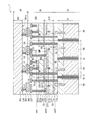
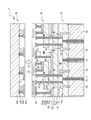
- FIG. 3 is a cross-sectional view in the thickness direction showing a configuration example of the image pickup apparatus 1 according to the first embodiment of the present disclosure.
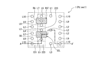
- FIG. 4A is a horizontal sectional view showing a configuration example of the pixel unit according to the first embodiment of the present disclosure.
- FIG. 4B is a horizontal sectional view showing a configuration example of the pixel unit according to the first embodiment of the present disclosure.
- FIG. 4C is a horizontal sectional view showing a configuration example of the pixel unit according to the first embodiment of the present disclosure.
- FIG. 4A is a horizontal sectional view showing a configuration example of the pixel unit according to the first embodiment of the present disclosure.
- FIG. 4B is a horizontal sectional view showing a configuration example of the pixel unit according to the
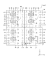
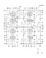
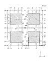
- FIG. 5 is a horizontal sectional view showing a layout example of a plurality of pixel units according to the first embodiment of the present disclosure.
- FIG. 6 is a horizontal sectional view showing a layout example of a plurality of pixel units according to the first embodiment of the present disclosure.
- FIG. 7 is a horizontal sectional view showing a layout example of a plurality of pixel units according to the first embodiment of the present disclosure.
- FIG. 8 is a cross-sectional view showing a method of manufacturing the image pickup apparatus according to the first embodiment of the present disclosure.
- FIG. 9 is a cross-sectional view showing a method of manufacturing the image pickup apparatus according to the first embodiment of the present disclosure.
- FIG. 10 is a cross-sectional view showing a method of manufacturing the image pickup apparatus according to the first embodiment of the present disclosure.
- FIG. 11 is a cross-sectional view showing a method of manufacturing the image pickup apparatus according to the first embodiment of the present disclosure.
- FIG. 12 is a cross-sectional view showing a method of manufacturing the image pickup apparatus according to the first embodiment of the present disclosure.
- FIG. 13 is a cross-sectional view showing a method of manufacturing the image pickup apparatus according to the first embodiment of the present disclosure.
- FIG. 14 is a cross-sectional view showing a method of manufacturing the image pickup apparatus according to the first embodiment of the present disclosure.
- FIG. 15 is a cross-sectional view showing a method of manufacturing the image pickup apparatus according to the second embodiment of the present disclosure.
- FIG. 16 is a cross-sectional view showing a method of manufacturing the image pickup apparatus according to the second embodiment of the present disclosure.
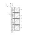
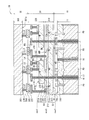
- FIG. 17 is a cross-sectional view in the thickness direction showing a configuration example of the image pickup apparatus according to the third embodiment of the present disclosure.
- FIG. 18 is a cross-sectional view in the thickness direction showing a configuration example of the image pickup apparatus according to the third embodiment of the present disclosure.
- FIG. 19 is a cross-sectional view in the thickness direction showing a configuration example of the image pickup apparatus according to the third embodiment of the present disclosure.
- FIG. 20 is a horizontal sectional view showing a layout example of a plurality of pixel units according to the third embodiment of the present disclosure.
- FIG. 21 is a horizontal sectional view showing a layout example of a plurality of pixel units according to the third embodiment of the present disclosure.
- FIG. 22 is a horizontal sectional view showing a layout example of a plurality of pixel units according to the third embodiment of the present disclosure.
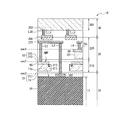
- FIG. 23 is a cross-sectional view in the thickness direction showing a configuration example of the image pickup apparatus according to the fourth embodiment of the present disclosure.
- the definition of the vertical direction in the following description is merely a definition for convenience of explanation, and does not limit the technical idea of the present disclosure. For example, if the object is rotated by 90 ° and observed, the top and bottom are converted to left and right and read, and if the object is rotated by 180 ° and observed, the top and bottom are reversed and read.
- the direction may be explained by using the wording in the X-axis direction, the Y-axis direction, and the Z-axis direction.
- the Z-axis direction is the thickness direction of the laminate including the first substrate portion 10 and the second substrate portion 20, which will be described later.
- the X-axis direction and the Y-axis direction are directions orthogonal to the Z-axis direction.
- the X-axis direction, the Y-axis direction, and the Z-axis direction are orthogonal to each other.
- the direction parallel to the X-axis direction and the Y-axis direction is also referred to as a horizontal direction.
- the plan view means the view from the Z-axis direction.
- FIG. 1 is a schematic view showing a configuration example of the image pickup apparatus 1 according to the first embodiment of the present disclosure.
- the image pickup apparatus 1 includes a first substrate portion 10, a second substrate portion 20, and a third substrate portion 30.
- the image pickup apparatus 1 is an image pickup apparatus having a three-dimensional structure, which is formed by laminating a first substrate portion 10, a second substrate portion 20, and a third substrate portion 30.
- the first substrate portion 10, the second substrate portion 20, and the third substrate portion 30 are laminated in this order.
- the first substrate portion 10 has a plurality of sensor pixels 12 that perform photoelectric conversion on the semiconductor substrate 11.
- the plurality of sensor pixels 12 are provided in a matrix in the pixel region 13 of the first substrate portion 10.
- the second substrate unit 20 has one readout circuit 22 for each of the four sensor pixels 12 that outputs a pixel signal based on the electric charge output from the sensor pixel 12.
- the second substrate portion 20 has a plurality of pixel drive lines 23 extending in the row direction and a plurality of vertical signal lines 24 extending in the column direction.
- the third substrate portion 30 may be referred to as a bottom substrate.
- the second substrate portion 20 has a structure in which two substrates are laminated, and has a lower substrate 210 and an upper substrate 220.
- the lower substrate 210 includes a first semiconductor substrate 211 (see FIG. 3), and the upper substrate 220 includes a second semiconductor substrate 221 (see FIG. 3).
- the first semiconductor substrate is provided with a first transistor included in the readout circuit 22 of the 211.
- the second semiconductor substrate 221 is provided with a second transition included in the readout circuit 22.
- the upper substrate 220 may be referred to as a top substrate.
- the lower substrate 210 may be referred to as a middle substrate.
- the third substrate portion 30 has a logic circuit 32 for processing a pixel signal on the semiconductor substrate 301.
- the logic circuit 32 includes, for example, a vertical drive circuit 33, a column signal processing circuit 34, a horizontal drive circuit 35, and a system control circuit 36.
- the logic circuit 32 (specifically, the horizontal drive circuit 35) outputs the output voltage Vout for each sensor pixel 12 to the outside.
- a low resistance region made of VDD formed by using a salicide (Self Aligned Silicide) process such as CoSi 2 or NiSi is formed. You may.
- the vertical drive circuit 33 selects a plurality of sensor pixels 12 in order in line units.
- the column signal processing circuit 34 for example, performs a correlated double sampling (CDS) process on a pixel signal output from each sensor pixel 12 in a row selected by the vertical drive circuit 33.
- the column signal processing circuit 34 extracts the signal level of the pixel signal by performing CDS processing, for example, and holds pixel data corresponding to the amount of light received by each sensor pixel 12.
- the horizontal drive circuit 35 sequentially outputs the pixel data held in the column signal processing circuit 34 to the outside, for example.
- the system control circuit 36 controls, for example, the drive of each block (vertical drive circuit 33, column signal processing circuit 34, and horizontal drive circuit 35) in the logic circuit 32.
- FIG. 2 is a circuit diagram showing a configuration example of the pixel unit PU according to the first embodiment of the present disclosure.
- the image pickup apparatus 1 in the image pickup apparatus 1, four sensor pixels 12 are electrically connected to one readout circuit 22 to form one pixel unit PU.
- the four sensor pixels 12 share one read circuit 22, and each output of the four sensor pixels 12 is input to the shared read circuit 22.
- Each sensor pixel 12 has a component common to each other.
- the identification numbers (1, 2, 3, FD) are added to the end of the code (for example, PD, TG, FD described later) of the component of each sensor pixel 12. 4) is given.
- an identification number is given at the end of the code of the component of each sensor pixel 12, but the components of each sensor pixel 12 are distinguished from each other. If it is not necessary to do so, the identification number at the end of the code of the component of each sensor pixel 12 shall be omitted.
- Each sensor pixel 12 receives, for example, a photodiode PD (an example of a photoelectric conversion element), a transfer transistor TR electrically connected to the photodiode PD, and a charge output from the photodiode PD via the transfer transistor TR. It has a floating diffusion FD that is temporarily held.
- the photodiode PD performs photoelectric conversion to generate an electric charge according to the amount of received light.
- the cathode of the photodiode PD is electrically connected to the source of the transfer transistor TR, and the anode of the photodiode PD is electrically connected to the reference potential line (eg, ground).
- the drain of the transfer transistor TR is electrically connected to the floating diffusion FD, and the gate electrode of the transfer transistor TR is electrically connected to the pixel drive line 23.
- the transfer transistor TR is, for example, a CMOS (Complementary Metal Oxide MOSFET) transistor.
- the floating diffusion FDs of the sensor pixels 12 sharing one read circuit 22 are electrically connected to each other and are also electrically connected to the input end of the common read circuit 22.
- the readout circuit 22 includes, for example, an amplification transistor AMP (an example of a first transistor), a reset transistor RST, and a selection transistor SEL (an example of a second transistor).
- the selection transistor SEL may be omitted if necessary.
- the source of the reset transistor RST (input end of the read circuit 22) is electrically connected to the floating diffusion FD, and the drain of the reset transistor RST is electrically connected to the power line VDD and the drain of the amplification transistor AMP.
- the gate electrode of the reset transistor RST is electrically connected to the pixel drive line 23 (see FIG. 1).
- the source of the amplification transistor AMP is electrically connected to the drain of the selection transistor SEL, and the gate electrode of the amplification transistor AMP is electrically connected to the source of the reset transistor RST.
- the source of the selection transistor SEL (the output end of the readout circuit 22) is electrically connected to the vertical signal line 24, and the gate electrode of the selection transistor SEL is electrically connected to the pixel drive line 23 (see FIG. 1). There is.
- the transfer transistor TR transfers the electric charge of the photodiode PD to the floating diffusion FD when the transfer transistor TR is turned on.
- the gate electrode TG of the transfer transistor TR extends from the surface of the semiconductor substrate 11 to a depth that penetrates the well layer WE and reaches the photodiode PD.
- the reset transistor RST resets the potential of the floating diffusion FD to a predetermined potential.
- the reset transistor RST is turned on, the potential of the floating diffusion FD is reset to the potential of the power supply line VDD.
- the selection transistor SEL controls the output timing of the pixel signal from the readout circuit 22.
- the amplification transistor AMP generates a voltage signal as a pixel signal according to the level of the electric charge held in the floating diffusion FD.
- the amplification transistor AMP constitutes a source follower type amplifier, and outputs a pixel signal having a voltage corresponding to the level of electric charge generated by the photodiode PD.
- the selection transistor SEL When the selection transistor SEL is turned on, the amplification transistor AMP amplifies the potential of the floating diffusion FD and outputs a voltage corresponding to the potential to the column signal processing circuit 34 via the vertical signal line 24.
- the reset transistor RST, amplification transistor AMP and selection transistor SEL are, for example, CMOS transistors.
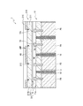
- FIG. 3 is a cross-sectional view in the thickness direction showing a configuration example of the image pickup apparatus 1 according to the first embodiment of the present disclosure.
- the cross-sectional view shown in FIG. 3 is merely a schematic view, and is not a diagram intended to show the actual structure exactly and correctly.
- the positions of the transistors and the impurity diffusion layer in the horizontal direction are intentionally changed at positions sec1 to sec3.
- the cross section at the position sec1 of the pixel unit PU shown in FIG. 3 is a cross section obtained by cutting FIG. 4A described later along the AA'line.
- the cross section at the position sec2 of the pixel unit PU shown in FIG. 3 is a cross section obtained by cutting FIG. 4B described later along the BB'line.
- the cross section at the position sec3 of the pixel unit PU shown in FIG. 3 is a cross section obtained by cutting FIG. 4C described later along the CC'line.
- FIGS. 4A to 4C show the structure of the image pickup apparatus 1 more accurately than FIG.
- the second substrate portion 20 is laminated on the front surface 10a (an example of one surface) side of the first substrate portion (bottom substrate) 10.
- a photodiode PD, a transfer transistor TR, and a floating diffusion FD are provided on the front surface 10a side of the first substrate portion 10.
- the photodiode PD, the transfer transistor TR, and the floating diffusion FD are each provided for each sensor pixel 12.
- the other surface (for example, the back surface) of the first substrate portion 10 is a light incident surface.
- the image pickup device 1 is a back-illuminated image pickup device, and is provided with a color filter and a light receiving lens on the back surface. A color filter and a light receiving lens are provided for each sensor pixel 12, respectively.
- the semiconductor substrate 11 included in the first substrate portion 10 is composed of, for example, a silicon substrate.
- a first conductive type (for example, p-type) well layer WE is provided in a part of the front surface of the semiconductor substrate 11 and its vicinity thereof, and a second conductive type (for example, p-type) well layer WE is provided in a region deeper than the well layer WE.
- an n-type photodiode PD is provided in the well layer WE.
- a well contact layer having a higher p-type concentration than the well layer WE and an n-type floating diffusion FD are provided. The well contact layer is provided to reduce the contact resistance between the well layer WE and the wiring.
- the semiconductor substrate 11 is provided with an element separation layer 16 that electrically separates sensor pixels 12 adjacent to each other.
- the element separation layer 16 has, for example, an STI (Shallow Trench Isolation) structure and extends in the depth direction of the semiconductor substrate 11.
- the element separation layer 16 is made of, for example, silicon oxide.
- an impurity diffusion layer 17 is provided between the element separation layer 16 and the photodiode PD.
- the impurity diffusion layer 17 has a p-type layer and an n-type layer extending in the thickness direction of the semiconductor substrate 11. The p-type layer is located on the element separation layer 16 side, and the n-type layer is located on the photodiode PD side.
- An insulating film 15 is provided on the front surface 11a side of the semiconductor substrate 11.
- the insulating film 15 is, for example, one of a silicon oxide film (SiO), a silicon nitride film (SiN), a silicon oxynitride film (SiON), or a silicon carbon nitride film (SiCN), or two or more of them. Is a laminated film.
- the second substrate portion 20 has a lower substrate (middle substrate) 210 and an upper substrate (top substrate) 220.
- the lower substrate 210 has a first semiconductor substrate 211.
- the first semiconductor substrate 211 is, for example, a silicon substrate made of single crystal silicon.
- An amplification transistor AMP and an element separation layer 213 surrounding the periphery of the amplification transistor AMP are provided on one surface (for example, the front surface 211a) of the first semiconductor substrate 211.
- One amplification transistor AMP and the other amplification transistor AMP of adjacent pixel unit PUs are electrically separated by the element separation layer 213.
- the lower substrate 210 has an insulating film 215 that covers the front surface 211a of the first semiconductor substrate 211.
- the amplifying transistor AMP and the element separation layer 213 are covered with the insulating film 215.
- the lower substrate 210 has an insulating film 217 that covers the other surface (for example, the back surface 211b) of the first semiconductor substrate 211.
- the insulating films 215 and 217 are, for example, one of SiO, SiN, SiON or SiCN, or a film in which two or more of these are laminated.
- the insulating film 15 of the first substrate portion 10 and the insulating film 217 of the lower substrate 210 are joined to each other to form an interlayer insulating film 51.
- the upper substrate 220 has a second semiconductor substrate 221.
- the second semiconductor substrate 221 is, for example, a silicon substrate made of single crystal silicon.
- a reset transistor RST, a selection transistor SEL, and an element separation layer 223 are provided on one surface (for example, the front surface 221a) of the second semiconductor substrate 221.
- the element separation layer 223 is provided between the reset transistor RST and the selection transistor SEL, and between the selection transistor SEL and the well layer of the second semiconductor substrate 221.
- the upper substrate 220 has an insulating film 225 that covers the front surface 221a, the back surface 221b, and the side surface of the second semiconductor substrate 221.
- the insulating film 225 is, for example, one of SiO, SiN, SiON or SiCN, or a film in which two or more of these are laminated.
- the insulating film 215 of the lower substrate 210 and the insulating film 225 of the upper substrate 220 are joined to each other to form an interlayer insulating film 53.
- the image pickup apparatus 1 is provided in the interlayer insulating films 51 and 53, and includes a plurality of wirings L1 to L10 that are electrically connected to at least one of the first substrate portion 10 and the second substrate portion 20.
- the wiring L1 electrically connects the drain of the amplification transistor AMP and the power supply line VDD.
- the wiring L2 electrically connects four floating diffusion FDs included in one pixel unit PU and the gate electrode AG of the amplification transistor AMP.
- the wiring L3 electrically connects the source of the amplification transistor AMP and the drain of the selection transistor SEL.
- the wiring L4 electrically connects the gate electrode SG of the selection transistor SEL and the pixel drive line 23 (see FIG. 1).
- the wiring L5 electrically connects the source of the selection transistor SEL and the vertical signal line 24.
- the wiring L6 electrically connects the drain of the reset transistor RST and the power supply line VDD.
- the wiring L7 electrically connects the gate electrode RG of the reset transistor RST (see FIG. 4A described later) and the pixel drive line 23.
- the wiring L8 electrically connects the source of the reset transistor RST and the wiring L2.
- the wiring L9 (an example of the first wiring) electrically connects the gate electrode TG of the transfer transistor TR and the pixel drive line 23 (see FIG. 1).
- the wiring L10 electrically connects the well contact layer and the reference potential line that supplies the reference potential (for example, the ground potential: 0 V).
- the portion extending in the thickness direction of the laminate is made of tungsten (W), and is extended in the direction orthogonal to the thickness direction of the laminate (for example, the horizontal direction).
- the portion is composed of copper (Cu) or a Cu alloy containing Cu as a main component.
- the materials constituting the wirings L1 to L10 are not limited to these, and may be composed of other materials.
- the second substrate portion 20 has a plurality of pad electrodes 227 connected to any wiring (for example, wirings L1, L4 to L7, L9, L10) among the wirings L1 to L10 described above.
- the plurality of pad electrodes 227 are made of, for example, Cu or a Cu alloy.
- the third substrate portion 30 is arranged on the opposite side (for example, the front surface side) of the surface of the second substrate portion 20 facing the first substrate portion 10.
- the third substrate portion 30 includes a semiconductor substrate 301, an insulating film 304 covering the front surface 301a side of the semiconductor substrate 301, and a plurality of wirings L30 provided on the front surface 301a side of the semiconductor substrate 301.
- a pad electrode 305 which is connected to each of the wirings L30, is provided.
- the third substrate portion 30 has the front surfaces bonded to each other with the second substrate portion 20. Therefore, in FIG. 3, the front surface 301a of the semiconductor substrate 301 faces downward.
- the semiconductor substrate 301 is, for example, a silicon substrate composed of single crystal silicon. On the front surface 301a side of the semiconductor substrate 301, a plurality of transistors and impurity diffusion layers constituting the logic circuit 32 (see FIG. 1) are provided.
- the insulating film 304 covers a plurality of transistors and an impurity diffusion layer constituting the logic circuit 32. The insulating film 304 is provided with contact holes for connecting these transistors and the impurity diffusion layer.
- Wiring L30 is provided in the contact hole.
- the portion extending in the thickness direction of the third substrate portion 30 is made of titanium (Ti) or cobalt (Co), and is in a direction orthogonal to the thickness direction of the third substrate portion 30 (for example).
- the portion extending in the horizontal direction) is composed of Cu or a Cu alloy containing Cu as a main component.
- the material constituting the wiring L30 is not limited to these, and may be composed of other materials.
- Silicide 39 (for example, titanium silicide (TiSi) or cobalt silicide (CoSi 2 )) is formed at the connection portion between the wiring L30 and the semiconductor substrate 301.
- the SiO39 connects the wiring L30 and the semiconductor substrate 301. It is closer to ohmic contact and the contact resistance is reduced. As a result, the calculation speed of the logic circuit 32 is increased.
- silicide is not formed on the first substrate portion 10 and the second substrate portion 20.
- heat treatment or the like can be performed at a temperature exceeding the heat resistant temperature of the silicide.
- the embodiment of the present disclosure is not limited to this, and SiO may be formed on at least one of the first substrate portion 10 and the second substrate portion 20.
- the plurality of pad electrodes 305 are made of, for example, Cu or a Cu alloy.
- the pad electrode 305 of the third substrate portion 30 faces the pad electrode 227 of the second substrate portion 20 and is electrically connected.
- the pad electrodes 305 and 227 are Cu-Cu bonded and integrated so as to face each other.
- the second substrate portion 20 and the third substrate portion 30 are electrically connected, and the strength of bonding between the second substrate portion 20 and the third substrate portion 30 is increased.
- FIG. 4A to 4C are horizontal cross-sectional views showing a configuration example of the pixel unit PU according to the first embodiment of the present disclosure. More specifically, FIG. 4A is a cross-sectional view of the pixel unit PU cut in the horizontal direction at the position sec1 shown in FIG. The position sec1 is at the same height as the upper surface of the gate electrode SG of the selection transistor SEL and the upper surface of the gate electrode RG of the reset transistor RST.
- FIG. 4B is a cross-sectional view of the pixel unit PU cut in the horizontal direction at the position sec2 shown in FIG. The position sec2 is a position at the same height as the upper surface of the gate electrode AG of the amplification transistor AMP.
- FIG. 4C is a cross-sectional view of the pixel unit PU cut in the horizontal direction at the position sec3 shown in FIG. The position sec1 is a position at the same height as the upper surface of the gate electrode TG of the transfer transistor TR.
- the transistor group including the selection transistor SEL and the reset transistor RST is located at the center of the pixel unit PU in a plan view.
- a wiring group including wirings L2, L9, and L10 is located outside the transistor group.
- This wiring group is arranged symmetrically with the transistor group including the selection transistor SEL and the reset transistor RST in between in a plan view. Further, the second semiconductor substrate 221 is provided with a well layer electrically separated from the source and drain of the transistor group by the element separation layer 223. This well layer is connected to a reference potential (for example, ground potential: 0 V) via the wiring L10.
- a reference potential for example, ground potential: 0 V
- the amplification transistor AMP is located at the center of the pixel unit PU in a plan view.
- the amplification transistor AMP, the selection transistor SEL, and the reset transistor RST are in a positional relationship of overlapping each other.
- a wiring group including wirings L2, L9, and L10 is located outside the amplification transistor AMP. This wiring group is arranged symmetrically with the amplification transistor AMP in between in a plan view.
- the four sensor pixels 12 included in one pixel unit PU are arranged close to each other via the element separation layer 16. Further, in each of the four sensor pixels 12, the gate electrode TG of the transfer transistor TR is interposed between the floating diffusion FD and the well layer WE in a plan view. The gate electrode TG separates the floating diffusion FD from the well layer WE. As shown in FIG. 3, the photodiode PD is located below the floating diffusion FD, the well layer WE, and the gate electrode TG.
- FIG. 5 to 7 are horizontal sectional views showing a layout example of a plurality of pixel unit PUs according to the first embodiment of the present disclosure. More specifically, FIG. 5 is a cross-sectional view of the image pickup apparatus 1 cut at the position sec3 shown in FIG.
- FIG. 6 is a cross-sectional view of the image pickup apparatus 1 cut at the position sec2 shown in FIG.
- FIG. 7 is a cross-sectional view of the first substrate portion 10 cut at the position sec1 shown in FIG.
- the plurality of pixel unit PUs are arranged side by side at regular intervals in the X-axis direction and the Y-axis direction, respectively.
- the pixel unit PUs are repeatedly arranged in the X-axis direction and the Y-axis direction, respectively.
- the imaging device 1 includes various film forming devices (including a CVD (Chemical Vapor Deposition) device and a sputtering device), an ion implantation device, a heat treatment device, an etching device, a CMP (Chemical Mechanical Polishing) device, a bonding device, and the like. Manufactured using equipment. Hereinafter, these devices are collectively referred to as manufacturing devices.
- FIG. 8 to 14 are cross-sectional views showing a manufacturing method of the image pickup apparatus 1 according to the first embodiment of the present disclosure.
- the manufacturing apparatus uses a CMOS process on the front surface 11a side of the semiconductor substrate 11, a well layer WE, an element separation layer 16, an impurity diffusion layer 17, a photodiode PD, and a transfer transistor TR.
- the gate electrode TG, the floating diffusion FD (see FIG. 4C), and the well contact layer are formed respectively.
- the manufacturing apparatus forms an insulating film 15 on the front surface 11a side of the semiconductor substrate 11 and flattens the surface thereof.
- the insulating film 15 is formed by the CVD method.
- the insulating film 15 is flattened by CMP. As a result, the first substrate portion 10 is completed.
- the manufacturing apparatus attaches the first semiconductor substrate 211 to the front surface 10a side of the first substrate portion 10.
- the back surface 211b of the first semiconductor substrate 211 is covered with an insulating film 217 such as a silicon oxide film (SiO).
- the front surface 11a of the semiconductor substrate 11 constituting the first substrate portion 10 and the back surface 211b of the first semiconductor substrate 211 face each other.
- the insulating film 15 covering the front surface 11a of the semiconductor substrate 11 and the insulating film 217 covering the back surface 211b of the first semiconductor substrate 211 are brought into close contact with each other to perform heat treatment. As a result, as shown in FIG.
- the insulating films 15 and 217 are integrated with each other to form an interlayer insulating film 51, and the semiconductor substrate 11 and the first semiconductor substrate 211 are joined to each other via the interlayer insulating film 51.
- the manufacturing apparatus grinds the front surface 211a side of the first semiconductor substrate 211 to make the first semiconductor substrate 211 thinner (that is, reduce the thickness). Foil thinning of the first semiconductor substrate 211 is performed by CMP.
- the manufacturing apparatus uses a CMOS process to form the element separation layer 213 and the amplification transistor AMP on the front surface 211a side of the foil-walled first semiconductor substrate 211.
- the manufacturing apparatus forms the gate electrode AG of the amplification transistor AMP on the front surface 221a of the second semiconductor substrate 221 after forming the element separation layer 213.
- the manufacturing apparatus forms the source and drain of the amplification transistor AMP on both sides of the gate electrode AG.
- the manufacturing apparatus forms an insulating film 215 on the front surface 221a side of the second semiconductor substrate 221 by the CVD method, and flattens the surface thereof by the CMP method.
- the manufacturing apparatus attaches the second semiconductor substrate 221 to the front surface 211a side of the first semiconductor substrate 211.
- the back surface 211b of the second semiconductor substrate 221 is covered with an insulating film 225A such as a silicon oxide film (SiO).
- the insulating film 225A is a part of the insulating film 225 (see FIG. 3).
- the front surface 211a of the first semiconductor substrate 211 and the back surface 221b of the second semiconductor substrate 221 face each other.
- the manufacturing apparatus the insulating film 215 covering the front surface 211a of the first semiconductor substrate 211 and the insulating film 225A covering the back surface 221b of the second semiconductor substrate 221 are brought into close contact with each other to perform heat treatment.
- the insulating films 215 and 225A are integrated with each other to form an interlayer insulating film 53, and the first semiconductor substrate 211 and the second semiconductor substrate 221 are bonded to each other via the interlayer insulating film 53.
- the manufacturing apparatus grinds the front surface 221a side of the second semiconductor substrate 221 to thin the second semiconductor substrate 221. Foil thinning of the second semiconductor substrate 221 is performed by CMP.
- the manufacturing apparatus partially removes the second semiconductor substrate 221 to form the second semiconductor substrate 221 in an island shape in a plan view. Partial removal of the second semiconductor substrate 221 is performed by forming a resist pattern using, for example, a photolithography technique, and dry-etching the second semiconductor substrate 221 using the resist pattern as a mask. In this dry etching, the insulating film 225A under the second semiconductor substrate 221 is used as an etching stopper.
- the manufacturing apparatus displays the element separation layer 223 and the selection transistor SEL on the front surface 221a side of the second semiconductor substrate 221.
- the reset transistor RST are formed using a CMOS process.
- the manufacturing apparatus forms the gate electrode SG of the selection transistor SEL and the gate electrode RG of the reset transistor RST on the front surface 221a of the second semiconductor substrate 221 after forming the element separation layer 213.
- the gate electrodes SG and RG may be formed at the same time in the same step.
- the manufacturing apparatus forms the source and drain of the selection transistor SEL on both sides of the gate electrode SG.
- the manufacturing apparatus forms the source and drain of the reset transistor RST on both sides of the gate electrode RG.
- the source and drain of the selection transistor SEL and the source and drain of the reset transistor RST may be formed at the same time in the same step.
- the step of forming the second semiconductor substrate 221 in an island shape may be performed before or after the step of forming the element separation layer 223, the selection transistor SEL, and the reset transistor RST, which will be described later. It may be done in parallel.
- the manufacturing apparatus sets the front surface of the second semiconductor substrate 221.
- An insulating film 225B is formed on the surface 221a side by the CVD method.
- the insulating film 225B is a part of the insulating film 225.
- the manufacturing apparatus flattens the surface of the insulating film 225B by the CMP method.
- the manufacturing apparatus forms the wirings L1 to L10 shown in FIGS. 3 and 4A to 4C, the plurality of pad electrodes 227, and the insulating film 225C.
- the insulating film 225C is a part of the insulating film 225.
- the manufacturing apparatus includes a step of forming a contact hole in an insulating film or a semiconductor substrate, a step of forming a metal material on the insulating film and in the contact hole, a step of patterning the metal material, a step of forming the insulating film, and insulation.
- the film flattening step is repeated a plurality of times.
- the wiring extending in the vertical direction is formed of tungsten (W), and the wiring extending in the horizontal direction and the pad electrode are formed of Cu or a Cu alloy.
- the manufacturing apparatus flattens the surface of the insulating film 225C by the CMP method to expose the front surface 227a of the pad electrode 227 from under the insulating film 225C. As a result, the second substrate portion 20 is completed.
- the manufacturing apparatus manufactures the third substrate portion 30 as shown in FIG.
- the manufacturing apparatus uses a CMOS process to form a logic circuit 32 (see FIG. 1) on the front surface 301a side of the semiconductor substrate 301.
- the silicide 39 is formed in the connection region between the semiconductor substrate 301 and the wiring L30.
- Silicide 39 is composed of a compound of a material constituting the semiconductor substrate 301 and a material constituting the wiring L30.
- a Salicide (Self Aligned Silicide) process such as CoSi 2 or NiSi is used to form VDD on the surface of the impurity diffusion region of the semiconductor substrate 301.
- the sensor pixel 12 is formed on the first substrate portion 10
- the readout circuit 22 is formed on the second substrate portion 20
- the logic circuit 32 is formed on the third substrate portion 30.
- Silicide is not formed in the sensor pixel 12 of the first substrate portion 10 or the readout circuit 22 of the second substrate portion 20. Therefore, in the step of forming the sensor pixel 12 and the readout circuit 22 described above, a high temperature process such as thermal oxidation can be performed without being limited by the heat resistant temperature of the silicide.
- the manufacturing apparatus mainly includes the front surface 301a of the semiconductor substrate 301 forming the third substrate portion 30 and the second semiconductor substrate 221 forming the second substrate portion 20.
- the surfaces 221a are opposed to each other.
- the manufacturing apparatus heat-treats the insulating film 304 located on the front surface 301a side of the semiconductor substrate 301 and the insulating film 225 located on the front surface 221a side of the second semiconductor substrate 221 in close contact with each other.
- the insulating films 304 and 225 are integrated with each other to form an interlayer insulating film, and the second semiconductor substrate 221 and the semiconductor substrate 301 are joined to each other via the interlayer insulating film.
- the semiconductor substrate 11 of the first substrate portion 10, the first semiconductor substrate 211 and the second semiconductor substrate 221 of the second substrate portion 20, and the semiconductor substrate 301 of the third substrate portion 30 are sequentially laminated via an insulating film.
- the pad electrode 305 of the third substrate portion 30 and the pad electrode 227 of the second substrate portion 20 are Cu-Cu bonded and integrated. This Cu-Cu bonding greatly contributes to the improvement of the bonding strength between the second substrate portion 20 and the third substrate portion 30.
- the image pickup apparatus 1 is completed through the above steps.
- the first substrate portion 10 provided with the sensor pixel 12 for performing photoelectric conversion and the front surface 12a side of the first substrate portion 10 It includes a second substrate portion 20 which is arranged and has a readout circuit 22 that outputs a pixel signal based on the charge output from the sensor pixel 12.
- the second substrate portion 20 is arranged on the front surface 211a side of the first semiconductor substrate 211 and the first semiconductor substrate 211 provided with the amplification transistor AMP included in the readout circuit 22, and is included in the readout circuit 22. It has a second semiconductor substrate 221 provided with a transistor SEL and a reset transistor RST.
- the area of the transistor arrangement area can be increased as compared with the case where all the transistors included in the readout circuit 22 are arranged on one semiconductor substrate, so that the layout of the readout circuit 22 can be freely arranged.
- the degree is improved.
- the gate area of the amplification transistor AMP can be maximized in each pixel unit PU, and good noise characteristics can be realized. By maximizing the area of the amplification transistor AMP, it is possible to reduce the random noise generated in the image pickup apparatus 1.
- the second semiconductor substrate 221 is laminated on the first semiconductor substrate 211.
- the manufacturing method of the second substrate portion 20 is not limited to this.
- the steps up to the step of forming the insulating film 215 on the front surface 221a side of the second semiconductor substrate 221 and flattening the surface thereof are the same as those in the first embodiment.
- the manufacturing apparatus forms the semiconductor film 221A on the insulating film 215.
- oxide semiconductors such as polysilicon (Poly-Si), polygermanium (Poly-Ge), and IGZO (InGaZNO), and 2D materials (thickness of only one to several atoms) are de facto. (Two-dimensional material), any one of Group III-V semiconductors, or a laminated film containing any one or more of these.
- the manufacturing apparatus partially removes the semiconductor film 221A to form the semiconductor film 221A in an island shape in a plan view. Partial removal of the semiconductor film 221A is performed by forming a resist pattern using, for example, a photolithography technique, and dry-etching the semiconductor film 221A using the resist pattern as a mask. In this dry etching, the insulating film 215 is used as an etching stopper.
- the manufacturing apparatus displays the element separation layer 223, the selection transistor SEL, and the reset transistor RST on the front surface 221Aa side of the semiconductor film 221A. (See FIG. 4A) and is formed using a CMOS process.
- the manufacturing apparatus forms the gate electrode SG of the selection transistor SEL and the gate electrode RG of the reset transistor RST on the front surface 221Aa of the semiconductor film 221A after forming the element separation layer 213.
- the gate electrodes SG and RG may be formed at the same time in the same step.
- the manufacturing apparatus forms the source and drain of the selection transistor SEL on both sides of the gate electrode SG.
- the manufacturing apparatus forms the source and drain of the reset transistor RST on both sides of the gate electrode RG.
- the source and drain of the selection transistor SEL and the source and drain of the reset transistor RST may be formed at the same time in the same step.
- the step of forming the semiconductor film 221A in an island shape may be performed before, after, or in parallel with the step of forming the element separation layer 223, the selection transistor SEL, and the reset transistor RST, which will be described later. You may go there.
- the manufacturing apparatus forms an insulating film 225B (see FIG. 12) on the front surface 221Aa side of the semiconductor film 221A and flattens the surface thereof.
- the manufacturing apparatus forms the wirings L1 to L10 shown in FIGS. 3 and 4A to 4C, the plurality of pad electrodes 227 (see FIG. 13), and the insulating film 225C (see FIG. 13).
- the manufacturing apparatus exposes the front surface 227a (see FIG. 13) of the pad electrode 227 from under the insulating film 225C.
- the second substrate portion 20 is completed.
- the manufacturing apparatus attaches the third substrate portion 30 to the second substrate portion 20.
- the image pickup apparatus 1A is completed.
- the image pickup apparatus 1A is arranged on the front surface 12a side of the first substrate portion 10 having the sensor pixels for performing photoelectric conversion and the first substrate portion 10, and is output from the sensor pixels 12.
- a second substrate portion 20A having a readout circuit 22 that outputs a pixel signal based on the charge is provided.
- the second substrate portion 20A is arranged on the front surface 211a side of the first semiconductor substrate 211 and the first semiconductor substrate 211 provided with the amplification transistor AMP included in the readout circuit 22, and is included in the readout circuit 22. It has a semiconductor film 221A provided with a transistor SEL and a reset transistor RST.
- the area of the transistor arrangement area can be increased as compared with the case where the transistors included in the readout circuit 22 are arranged only on the substrate surface, the degree of freedom in the layout of the readout circuit 22 is improved. ..
- the gate area of the amplification transistor AMP can be maximized in each pixel unit PU, and good noise characteristics can be realized. By maximizing the area of the amplification transistor AMP, it is possible to reduce the random noise generated in the image pickup apparatus 1.
- the noise characteristics required for selection transistors and reset transistors are not strict. Therefore, even when the selection transistor SEL and the reset transistor RST are formed on the semiconductor film 221A such as polysilicon instead of the single crystal semiconductor substrate as in the second embodiment, the image pickup apparatus 1A realizes good noise characteristics. be able to.
- the wiring L2 that is, the contact for floating diffusion
- the wiring L10 that is, the wiring L10 electrically connected to the well layer WE
- a well contact and one each are arranged (see FIG. 4).
- one floating diffusion contact may be arranged for each of the plurality of sensor pixels 12. For example, four sensor pixels 12 adjacent to each other may share one floating diffusion contact.
- one well contact may be arranged for each of the plurality of sensor pixels 12. For example, four sensor pixels 12 adjacent to each other may share one well contact.
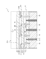
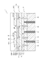
- FIGS. 17 to 19 are cross-sectional views in the thickness direction showing a configuration example of the image pickup apparatus 1B according to the third embodiment of the present disclosure.
- 20 to 22 are horizontal sectional views showing a layout example of the plurality of pixel unit PUs according to the third embodiment of the present disclosure.
- the cross-sectional views shown in FIGS. 17 to 19 are merely schematic views, and are not intended to show the actual structure exactly and correctly.
- the cross-sectional views shown in FIGS. 17 to 19 intentionally change the positions of the transistors and the impurity diffusion layer in the horizontal direction at positions sec1 to sec3 in order to explain the configuration of the image pickup apparatus 1B on paper in an easy-to-understand manner. ..
- the cross section at position sec1 is a cross section obtained by cutting FIG. 20 along the line A1-A1'
- the cross section at position sec2 is a cross section shown in FIG. 21 at B1-B1'. It is a cross section cut by a line
- the cross section at position sec3 is a cross section of FIG. 22 cut along the C1-C1'line.
- the cross section at position sec1 is a cross section obtained by cutting FIG. 20 along the A2-A2'line
- the cross section at position sec2 is a cross section obtained by cutting FIG. 21 along the B2-B2' line.
- the cross section at position sec3 is a cross section of FIG. 22 cut along the C2-C2'line.
- the cross section at position sec1 is a cross section obtained by cutting FIG. 20 along the line A3-A3'
- the cross section at position sec2 is a cross section obtained by cutting FIG. 21 along the line B3-B3'.
- the cross section at sec3 is a cross section obtained by cutting FIG. 22 along the C3-C3'line.
- the image pickup apparatus 1B includes a common pad electrode 102 (an example of the “first common pad electrode” of the present disclosure) arranged so as to straddle a plurality of sensor pixels 12, and a common pad electrode. It shares with one wiring L2 provided on 102.
- the image pickup apparatus 1B has a region in which the floating diffusion FD1 to FD4 of the four sensor pixels 12 are adjacent to each other via the element separation layer 16 in a plan view.
- a common pad electrode 102 is provided in this region.
- the common pad electrode 102 is arranged so as to straddle the four floating diffusion FD1 to FD4, and is electrically connected to each of the four floating diffusion FD1 to FD4.
- the common pad electrode 102 is composed of, for example, a polysilicon film doped with n-type impurities or p-type impurities.
- One wiring L2 (that is, a contact for floating diffusion) is provided on the center of the common pad electrode 102. As shown in FIGS. 18 and 20 to 22, the wiring L2 provided on the central portion of the common pad electrode 102 penetrates from the first substrate portion 10 to the lower substrate 210 of the second substrate portion 20. 2 It extends to the upper substrate 220 of the substrate portion 20 and is connected to the gate electrode AG of the amplification transistor AMP via wiring or the like provided on the upper substrate 220.
- the image pickup apparatus 1B is common with the common pad electrode 110 (an example of the “second common pad electrode” of the present disclosure) arranged so as to straddle the plurality of sensor pixels 12. It shares with one wiring L10 provided on the pad electrode 110.
- each well layer WE of the four sensor pixels 12 has a region adjacent to each other via the element separation layer 16.
- a common pad electrode 110 is provided in this area.
- the common pad electrode 110 is arranged so as to straddle each well layer WE of the four sensor pixels 12, and is electrically connected to each well layer WE of the four sensor pixels 12.
- the common pad electrode 110 is arranged between one common pad electrode 102 arranged in the Y-axis direction and another common pad electrode 102. In the Y-axis direction, the common pad electrodes 102 and 110 are arranged alternately side by side.
- the common pad electrode 110 is composed of, for example, a polysilicon film doped with n-type impurities or p-type impurities.
- One wiring L10 (that is, a well contact) is provided on the center of the common pad electrode 110. As shown in FIGS. 17 and 19 to 22, the wiring L10 provided on the central portion of the common pad electrode 110 penetrates from the first substrate portion 10 to the lower substrate 210 of the second substrate portion 20. 2 It extends to the upper substrate 220 of the substrate portion 20 and is connected to a reference potential line for supplying a reference potential (for example, ground potential: 0 V) via wiring or the like provided on the upper substrate 220.
- a reference potential line for supplying a reference potential (for example, ground potential: 0 V) via wiring or the like provided on the upper substrate 220.
- the wiring L10 provided on the central portion of the common pad electrode 110 includes the upper surface of the common pad electrode 110, the inner side surface of the through hole provided in the lower substrate 210, and the inside of the through hole provided in the upper substrate 220. Each is electrically connected to the side surface.
- the well layer WE of the semiconductor substrate 11 of the first substrate portion 10, the well layer of the lower substrate 210 of the second substrate portion 20, and the well layer of the upper substrate 220 have a reference potential (for example, ground potential: 0 V). Connected to.
- the image pickup device 1B according to the third embodiment of the present disclosure has the same effect as the image pickup device 1 according to the first embodiment. Further, the image pickup apparatus 1B is provided on the front surface 11a side of the semiconductor substrate 11 constituting the first substrate portion 10, and is arranged so as to straddle a plurality of (for example, four) sensor pixels 12 adjacent to each other.
- the common pad electrodes 102 and 110 are further provided.
- the common pad electrode 102 is electrically connected to the floating diffusion FD of the four sensor pixels 12.
- the common pad electrode 110 is electrically connected to the well layer WE of the four sensor pixels 12.
- the wiring L2 connected to the floating diffusion FD can be shared for each of the four sensor pixels 12.
- the wiring L10 connected to the well layer WE can be shared for each of the four sensor pixels 12.
- the number of wirings L2 and L10 can be reduced, so that the area of the sensor pixel 12 can be reduced and the image pickup device 1B can be miniaturized.
- the semiconductor substrate 11 is provided with the element separation layer 16 that electrically separates the sensor pixels 12 adjacent to each other.
- the element separation layer 16 may be provided from the front surface 11a to the back surface 11b of the semiconductor substrate 11, or may be provided from the back surface 11b toward the front surface 11a. You may.
- the image pickup apparatus 1 according to the first embodiment has, for example, a structure in which an element separation layer 16 is provided from the front surface 11a to the back surface 11b of the semiconductor substrate 11.
- a structure in which the element separation layer 16 is provided from the back surface 11b of the semiconductor substrate 11 toward the front surface 11a is illustrated.
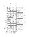
- FIG. 23 is a cross-sectional view in the thickness direction showing a configuration example of the image pickup apparatus 1C according to the fourth embodiment of the present disclosure.
- the element separation layer 16 is provided from the back surface 11b (that is, the light incident surface) of the semiconductor substrate 11 toward the front surface 11a.
- the element separation layer 16 is a DTI (Deep Trench Isolation).
- the element separation layer 16 is formed by forming a deep trench from the back surface 11b toward the front surface 11a and embedding an insulating film such as silicon oxide in the deep trench. Even with such a configuration, the image pickup apparatus 1C has the same effect as that of the image pickup apparatus 1 according to the first embodiment.
- FIG. 23 shows a structure in which the element separation layer 16 is provided from the back surface 11b of the semiconductor substrate 11 to the inside of the semiconductor substrate 11, but this is just an example.
- the element separation layer 16 may reach the front surface 11a of the semiconductor substrate 11. That is, the element separation layer 16 may penetrate the semiconductor substrate 11.
- the first semiconductor substrate 211 is provided with the amplification transistor AMP
- the second semiconductor substrate 221 is provided with the selection transistor SEL and the reset transistor RST.
- the selection transistor SEL and the reset transistor RST may be provided on the first semiconductor substrate 211
- the amplification transistor AMP may be provided on the second semiconductor substrate 221.
- the first semiconductor substrate 211 may be provided with one of the selection transistor SEL and the reset transistor RST and the amplification transistor AMP
- the second semiconductor substrate 221 may be provided with the other of the selection transistor SEL and the reset transistor RST.
- the amplification transistor AMP is provided on the first semiconductor substrate 211, and the selection transistor SEL and the reset transistor RST are provided on the semiconductor film 221A.
- the selection transistor SEL and the reset transistor RST may be provided on the first semiconductor substrate 211, and the amplification transistor AMP may be provided on the semiconductor film 221A.
- one of the selection transistor SEL and the reset transistor RST and the amplification transistor AMP may be provided on the first semiconductor substrate 211, and the other of the selection transistor SEL and the reset transistor RST may be provided on the semiconductor film 221A.
- the present technology includes various embodiments not described here. At least one of the various omissions, substitutions and modifications of the components may be made without departing from the gist of the embodiments and modifications described above. Further, the effects described in the present specification are merely examples and are not limited, and other effects may be obtained.
- the present disclosure may also have the following structure.
- the second substrate portion is A first semiconductor substrate provided with a first transistor included in the readout circuit, and
- An image pickup apparatus having a second semiconductor substrate arranged on one surface side of the first semiconductor substrate and provided with a second transistor included in the readout circuit.
- the second substrate portion is A first semiconductor substrate provided with a first transistor included in the readout circuit, and An image pickup apparatus having a semiconductor film arranged on one surface side of the first semiconductor substrate and provided with a second transistor included in the readout circuit.
- the sensor pixel is Photoelectric conversion element and A transfer transistor electrically connected to the photoelectric conversion element, It has a floating diffusion that temporarily holds the electric charge output from the photoelectric conversion element via the transfer transistor.
- the read circuit A reset transistor that resets the potential of the floating diffusion to a predetermined potential, and As the pixel signal, an amplification transistor that generates a voltage signal corresponding to the level of electric charge held in the floating diffusion, and It has a selection transistor that controls the output timing of the pixel signal from the amplification transistor.
- the first transistor is the amplification transistor and The imaging device according to any one of (1) to (3) above, wherein the second transistor is the reset transistor and the selection transistor.
- One of the readout circuits is electrically connected to the plurality of the sensor pixels to form one pixel unit.
- the laminated body has a wiring group that is electrically connected to the sensor pixel.
- a third substrate portion which is arranged on the opposite side of the surface of the second substrate portion facing the first substrate portion, is further provided.
- the imaging device according to any one of (1) to (6) above, wherein a logic circuit for processing the pixel signal is provided on the third substrate portion.
- a logic circuit for processing the pixel signal is provided on the third substrate portion.
- the third substrate portion is provided with VDD.
- a first common pad electrode which is provided on one surface side of the first substrate portion and is arranged so as to straddle the plurality of sensor pixels adjacent to each other, is further provided.
- the sensor pixel is Photoelectric conversion element and A transfer transistor electrically connected to the photoelectric conversion element, It has a floating diffusion that temporarily holds the electric charge output from the photoelectric conversion element via the transfer transistor.
- the first common pad electrode is electrically connected to the floating diffusion of a plurality of the sensor pixels.
- the sensor pixel has a well layer and The imaging device according to any one of (1) to (9), wherein the second common pad electrode is electrically connected to the well layer of the plurality of sensor pixels.
- An element separation layer provided on the first substrate portion and provided between a plurality of sensor pixels adjacent to each other is further provided. Any one of (1) to (10) above, wherein the element separation layer is provided from one surface of the first substrate portion toward the other surface located on the opposite side of the one surface.
- the imaging device according to. (12) An element separation layer provided on the first substrate portion and provided between a plurality of sensor pixels adjacent to each other is further provided. Any one of (1) to (10) above, wherein the element separation layer is provided from the other surface located on the opposite side of one surface of the first substrate portion toward one surface.
- Imaging device 3 Column signal processing circuit 10 1st substrate (bottom substrate) 10a, 11a, 12a, 221a, 221a, 221Aa, 227a, 301a Front surface 11, 301 Semiconductor substrate 12 Sensor pixel 13 Pixel region 15, 215, 217, 225, 225A, 225B, 225C, 304 Insulating film 16, 213 , 223 Element separation layer 17 Impure diffusion layer 20, 20A Second board section 22 Read circuit 23 Pixel drive line 24 Vertical signal line 30 Third board section 32 Logic circuit 33 Vertical drive circuit 34 Column signal processing circuit 35 Horizontal drive circuit 36 system Control circuit 39 VDD51, 53 Interlayer insulating film 102, 110 Common pad electrode 210 Lower substrate (middle substrate) 211 First semiconductor substrate 11b, 211b, 221b Back surface 220 Upper substrate (top substrate) 221 Second semiconductor substrate 221A Semiconductor film 227, 305 Pad electrode AG Gate electrode AMP Amplification transistor FD Floating diffusion L1 to L10, L30 Wiring
Landscapes
- Engineering & Computer Science (AREA)
- Multimedia (AREA)
- Signal Processing (AREA)
- Solid State Image Pick-Up Elements (AREA)
- Transforming Light Signals Into Electric Signals (AREA)
- Internal Circuitry In Semiconductor Integrated Circuit Devices (AREA)
Abstract
Description
図1は、本開示の実施形態1に係る撮像装置1の構成例を示す模式図である。撮像装置1は、第1基板部10と、第2基板部20と、第3基板部30とを備えている。撮像装置1は、第1基板部10と、第2基板部20と、第3基板部30とを貼り合わせて構成された3次元構造の撮像装置である。第1基板部10と、第2基板部20と、第3基板部30は、この順に積層されている。
上記の実施形態1では、第2基板部20の製造方法として、第1半導体基板211上に第2半導体基板221を積層することを説明した。しかしながら、本開示の実施形態において、第2基板部20の製造方法はこれに限定されない。
上記の実施形態1では、複数のセンサ画素12の各々に、フローティングディフュージョンFDに電気的に接続する配線L2(すなわち、フローティングディフュージョン用コンタクト)と、ウェル層WEに電気的に接続する配線L10(すなわち、ウェル用コンタクト)とがそれぞれ1つずつ配置される構造を説明した(図4参照)。しかしながら、本開示の実施形態はこれに限定されない。本開示の実施形態では、複数のセンサ画素12ごとに、1つのフローティングディフュージョン用コンタクトが配置されていてもよい。例えば、互いに隣り合う4つのセンサ画素12が、1つのフローティングディフュージョン用コンタクトを共有していてもよい。同様に、複数のセンサ画素12ごとに、1つのウェル用コンタクトが配置されていてもよい。例えば、互いに隣り合う4つのセンサ画素12が、1つのウェル用コンタクトを共有していてもよい。
上記の実施形態1では、互いに隣り合うセンサ画素12同士を電気的に分離する素子分離層16が半導体基板11に設けられていることを説明した。本開示の実施形態では、素子分離層16は、半導体基板11のおもて面11aから裏面11bに向けて設けられていてもよいし、裏面11bからおもて面11aに向けて設けられていてもよい。実施形態1に係る撮像装置1は、例えば、半導体基板11のおもて面11aから裏面11bに向けて素子分離層16が設けられた構造である。実施形態4では、半導体基板11の裏面11bからおもて面11aに向けて素子分離層16が設けられた構造を例示する。
上記のように、本開示は実施形態及び変形例によって記載したが、この開示の一部をなす論述及び図面は本開示を限定するものであると理解すべきではない。この開示から当業者には様々な代替実施の形態、実施例及び運用技術が明らかとなろう。
(1)光電変換を行うセンサ画素を有する第1基板部と、
前記第1基板部の一方の面側に配置され、前記センサ画素から出力された電荷に基づく画素信号を出力する読み出し回路を有する第2基板部と、を備え、
前記第2基板部は、
前記読み出し回路に含まれる第1トランジスタが設けられた第1半導体基板と、
前記第1半導体基板の一方の面側に配置され、前記読み出し回路に含まれる第2トランジスタが設けられた第2半導体基板と、を有する撮像装置。
(2)光電変換を行うセンサ画素を有する第1基板部と、
前記第1基板部の一方の面側に配置され、前記センサ画素から出力された電荷に基づく画素信号を出力する読み出し回路を有する第2基板部と、を備え、
前記第2基板部は、
前記読み出し回路に含まれる第1トランジスタが設けられた第1半導体基板と、
前記第1半導体基板の一方の面側に配置され、前記読み出し回路に含まれる第2トランジスタが設けられた半導体膜と、を有する撮像装置。
(3)前記第2基板部の厚さ方向において、前記第1トランジスタと前記第2トランジスタは互いに重なる、前記(1)又は(2)に記載の撮像装置。
(4)前記センサ画素は、
光電変換素子と、
前記光電変換素子と電気的に接続された転送トランジスタと、
前記転送トランジスタを介して前記光電変換素子から出力された電荷を一時的に保持するフローティングディフュージョンと、を有し、
前記読み出し回路は、
前記フローティングディフュージョンの電位を所定の電位にリセットするリセットトランジスタと、
前記画素信号として、前記フローティングディフュージョンに保持された電荷のレベルに応じた電圧の信号を生成する増幅トランジスタと、
前記増幅トランジスタからの前記画素信号の出力タイミングを制御する選択トランジスタと、を有し、
前記第1トランジスタは、前記増幅トランジスタであり、
前記第2トランジスタは、前記リセットトランジスタ及び前記選択トランジスタである、前記(1)から(3)のいずれか1項に記載の撮像装置。
(5)複数の前記センサ画素に1つの前記読み出し回路が電気的に接続されて、1つの画素ユニットを構成しており、
前記第1基板部及び前記第2基板部を含む積層体の厚さ方向からの平面視で、前記画素ユニットの中心部に前記増幅トランジスタが位置する、前記(4)に記載の撮像装置。
(6)前記積層体は、前記センサ画素に電気的に接続する配線群、を有し、
前記配線群の少なくとも一部は、前記積層体の厚さ方向からの平面視で、前記増幅トランジスタを挟んで左右対称に配置されている、前記(5)に記載の撮像装置。
(7)前記第2基板部において前記第1基板部と向かい合う面の反対側に配置される第3基板部、をさらに備え、
前記第3基板部には、前記画素信号を処理するロジック回路が設けられている、前記(1)から(6)のいずれか1項に記載の撮像装置。
(8)前記第3基板部にシリサイドが設けられている、前記(7)に記載の撮像装置。
(9)前記第1基板部の一方の面側に設けられ、互いに隣り合う複数の前記センサ画素に跨るように配置された第1共通パッド電極、をさらに備え、
前記センサ画素は、
光電変換素子と、
前記光電変換素子と電気的に接続された転送トランジスタと、
前記転送トランジスタを介して前記光電変換素子から出力された電荷を一時的に保持するフローティングディフュージョンと、を有し、
前記第1共通パッド電極は、複数の前記センサ画素の前記フローティングディフュージョンに電気的に接続する、前記(1)から(8)のいずれか1項に記載の撮像装置。
(10)前記第1基板部の一方の面側に設けられ、互いに隣り合う複数の前記センサ画素に跨るように配置された第2共通パッド電極、をさらに備え、
前記センサ画素はウェル層を有し、
前記第2共通パッド電極は、複数の前記センサ画素の前記ウェル層に電気的に接続する、前記(1)から(9)のいずれか1項に記載の撮像装置。
(11)前記第1基板部に設けられ、互いに隣り合う複数の前記センサ画素間に設けられた素子分離層、をさらに備え、
前記素子分離層は、前記第1基板部の一方の面から、一方の面の反対側に位置する他方の面に向けて設けられている、前記(1)から(10)のいずれか1項に記載の撮像装置。
(12)前記第1基板部に設けられ、互いに隣り合う複数の前記センサ画素間に設けられた素子分離層、をさらに備え、
前記素子分離層は、前記第1基板部の一方の面の反対側に位置する他方の面から、一方の面に向けて設けられている、前記(1)から(10)のいずれか1項に記載の撮像装置。
3 カラム信号処理回路
10 第1基板部(ボトム基板)
10a、11a、12a、221a、221a、221Aa、227a、301a おもて面
11、301 半導体基板
12 センサ画素
13 画素領域
15、215、217、225、225A、225B、225C、304 絶縁膜
16、213、223 素子分離層
17 不純物拡散層
20、20A 第2基板部
22 読み出し回路
23 画素駆動線
24 垂直信号線
30 第3基板部
32 ロジック回路
33 垂直駆動回路
34 カラム信号処理回路
35 水平駆動回路
36 システム制御回路
39 シリサイド
51、53 層間絶縁膜
102、110 共通パッド電極
210 下側基板(ミドル基板)
211 第1半導体基板
11b、211b、221b 裏面
220 上側基板(トップ基板)
221 第2半導体基板
221A 半導体膜
227、305 パッド電極
AG ゲート電極
AMP 増幅トランジスタ
FD フローティングディフュージョン
L1からL10、L30 配線
PD フォトダイオード
PU 画素ユニット
RG ゲート電極
RST リセットトランジスタ
sec1、sec2、sec3 位置
SEL 選択トランジスタ
SG ゲート電極
TG ゲート電極
TR 転送トランジスタ
VDD 電源線
Vout 出力電圧
WE ウェル層
Claims (12)
- 光電変換を行うセンサ画素を有する第1基板部と、
前記第1基板部の一方の面側に配置され、前記センサ画素から出力された電荷に基づく画素信号を出力する読み出し回路を有する第2基板部と、を備え、
前記第2基板部は、
前記読み出し回路に含まれる第1トランジスタが設けられた第1半導体基板と、
前記第1半導体基板の一方の面側に配置され、前記読み出し回路に含まれる第2トランジスタが設けられた第2半導体基板と、を有する撮像装置。 - 光電変換を行うセンサ画素を有する第1基板部と、
前記第1基板部の一方の面側に配置され、前記センサ画素から出力された電荷に基づく画素信号を出力する読み出し回路を有する第2基板部と、を備え、
前記第2基板部は、
前記読み出し回路に含まれる第1トランジスタが設けられた第1半導体基板と、
前記第1半導体基板の一方の面側に配置され、前記読み出し回路に含まれる第2トランジスタが設けられた半導体膜と、を有する撮像装置。 - 前記第2基板部の厚さ方向において、前記第1トランジスタと前記第2トランジスタは互いに重なる、請求項1に記載の撮像装置。
- 前記センサ画素は、
光電変換素子と、
前記光電変換素子と電気的に接続された転送トランジスタと、
前記転送トランジスタを介して前記光電変換素子から出力された電荷を一時的に保持するフローティングディフュージョンと、を有し、
前記読み出し回路は、
前記フローティングディフュージョンの電位を所定の電位にリセットするリセットトランジスタと、
前記画素信号として、前記フローティングディフュージョンに保持された電荷のレベルに応じた電圧の信号を生成する増幅トランジスタと、
前記増幅トランジスタからの前記画素信号の出力タイミングを制御する選択トランジスタと、を有し、
前記第1トランジスタは、前記増幅トランジスタであり、
前記第2トランジスタは、前記リセットトランジスタ及び前記選択トランジスタである、請求項1に記載の撮像装置。 - 複数の前記センサ画素に1つの前記読み出し回路が電気的に接続されて、1つの画素ユニットを構成しており、
前記第1基板部及び前記第2基板部を含む積層体の厚さ方向からの平面視で、前記画素ユニットの中心部に前記増幅トランジスタが位置する、請求項4に記載の撮像装置。 - 前記積層体は、前記センサ画素に電気的に接続する配線群、を有し、
前記配線群の少なくとも一部は、前記積層体の厚さ方向からの平面視で、前記増幅トランジスタを挟んで左右対称に配置されている、請求項5に記載の撮像装置。 - 前記第2基板部において前記第1基板部と向かい合う面の反対側に配置される第3基板部、をさらに備え、
前記第3基板部には、前記画素信号を処理するロジック回路が設けられている、請求項1に記載の撮像装置。 - 前記第3基板部にシリサイドが設けられている、請求項7に記載の撮像装置。
- 前記第1基板部の一方の面側に設けられ、互いに隣り合う複数の前記センサ画素に跨るように配置された第1共通パッド電極、をさらに備え、
前記センサ画素は、
光電変換素子と、
前記光電変換素子と電気的に接続された転送トランジスタと、
前記転送トランジスタを介して前記光電変換素子から出力された電荷を一時的に保持するフローティングディフュージョンと、を有し、
前記第1共通パッド電極は、複数の前記センサ画素の前記フローティングディフュージョンに電気的に接続する、請求項1に記載の撮像装置。 - 前記第1基板部の一方の面側に設けられ、互いに隣り合う複数の前記センサ画素に跨るように配置された第2共通パッド電極、をさらに備え、
前記センサ画素はウェル層を有し、
前記第2共通パッド電極は、複数の前記センサ画素の前記ウェル層に電気的に接続する、請求項1に記載の撮像装置。 - 前記第1基板部に設けられ、互いに隣り合う複数の前記センサ画素間に設けられた素子分離層、をさらに備え、
前記素子分離層は、前記第1基板部の一方の面から、一方の面の反対側に位置する他方の面に向けて設けられている、請求項1に記載の撮像装置。 - 前記第1基板部に設けられ、互いに隣り合う複数の前記センサ画素間に設けられた素子分離層、をさらに備え、
前記素子分離層は、前記第1基板部の一方の面の反対側に位置する他方の面から、一方の面に向けて設けられている、請求項1に記載の撮像装置。
Priority Applications (6)
| Application Number | Priority Date | Filing Date | Title |
|---|---|---|---|
| CN202080026142.9A CN113711338B (zh) | 2019-04-25 | 2020-04-24 | 摄像装置 |
| US17/601,563 US11961864B2 (en) | 2019-04-25 | 2020-04-24 | Imaging device with improved layout of reading circuit transistors |
| KR1020217033162A KR102783039B1 (ko) | 2019-04-25 | 2020-04-24 | 촬상 장치 |
| KR1020257007043A KR20250039480A (ko) | 2019-04-25 | 2020-04-24 | 촬상 장치 |
| DE112020002090.8T DE112020002090T5 (de) | 2019-04-25 | 2020-04-24 | Bildgebungsvorrichtung |
| US18/596,343 US20240213284A1 (en) | 2019-04-25 | 2024-03-05 | Imaging device |
Applications Claiming Priority (2)
| Application Number | Priority Date | Filing Date | Title |
|---|---|---|---|
| JP2019-084191 | 2019-04-25 | ||
| JP2019084191A JP2020182112A (ja) | 2019-04-25 | 2019-04-25 | 撮像装置 |
Related Child Applications (2)
| Application Number | Title | Priority Date | Filing Date |
|---|---|---|---|
| US17/601,563 A-371-Of-International US11961864B2 (en) | 2019-04-25 | 2020-04-24 | Imaging device with improved layout of reading circuit transistors |
| US18/596,343 Continuation US20240213284A1 (en) | 2019-04-25 | 2024-03-05 | Imaging device |
Publications (1)
| Publication Number | Publication Date |
|---|---|
| WO2020218503A1 true WO2020218503A1 (ja) | 2020-10-29 |
Family
ID=72942806
Family Applications (1)
| Application Number | Title | Priority Date | Filing Date |
|---|---|---|---|
| PCT/JP2020/017677 Ceased WO2020218503A1 (ja) | 2019-04-25 | 2020-04-24 | 撮像装置 |
Country Status (6)
| Country | Link |
|---|---|
| US (2) | US11961864B2 (ja) |
| JP (1) | JP2020182112A (ja) |
| KR (2) | KR20250039480A (ja) |
| CN (1) | CN113711338B (ja) |
| DE (1) | DE112020002090T5 (ja) |
| WO (1) | WO2020218503A1 (ja) |
Cited By (2)
| Publication number | Priority date | Publication date | Assignee | Title |
|---|---|---|---|---|
| WO2022202127A1 (ja) * | 2021-03-23 | 2022-09-29 | ソニーセミコンダクタソリューションズ株式会社 | 撮像素子及び撮像装置 |
| JPWO2022265059A1 (ja) * | 2021-06-16 | 2022-12-22 |
Families Citing this family (7)
| Publication number | Priority date | Publication date | Assignee | Title |
|---|---|---|---|---|
| JP7042885B1 (ja) * | 2020-10-30 | 2022-03-28 | 株式会社大都技研 | 遊技台 |
| KR20230098578A (ko) * | 2020-11-12 | 2023-07-04 | 소니 세미컨덕터 솔루션즈 가부시키가이샤 | 촬상 소자 및 촬상 장치 |
| US12568706B2 (en) * | 2021-08-12 | 2026-03-03 | Taiwan Semiconductor Manufacturing Company, Ltd. | Semiconductor device including image sensor and methods of forming the same |
| KR102942181B1 (ko) * | 2021-09-08 | 2026-03-19 | 삼성전자주식회사 | 이미지 센서 |
| KR20240086387A (ko) * | 2022-12-09 | 2024-06-18 | 삼성전자주식회사 | 이미지 센서 |
| WO2024142692A1 (ja) * | 2022-12-28 | 2024-07-04 | ソニーセミコンダクタソリューションズ株式会社 | 固体撮像装置 |
| KR20240166314A (ko) * | 2023-05-17 | 2024-11-26 | 삼성전자주식회사 | 이미지 센서 |
Citations (3)
| Publication number | Priority date | Publication date | Assignee | Title |
|---|---|---|---|---|
| JP2016086164A (ja) * | 2014-10-24 | 2016-05-19 | 株式会社半導体エネルギー研究所 | 撮像装置および電子機器 |
| JP2018148116A (ja) * | 2017-03-08 | 2018-09-20 | ソニーセミコンダクタソリューションズ株式会社 | 固体撮像装置、および電子機器 |
| JP2019004001A (ja) * | 2017-06-13 | 2019-01-10 | ルネサスエレクトロニクス株式会社 | 固体撮像素子およびその製造方法 |
Family Cites Families (15)
| Publication number | Priority date | Publication date | Assignee | Title |
|---|---|---|---|---|
| US6021172A (en) * | 1994-01-28 | 2000-02-01 | California Institute Of Technology | Active pixel sensor having intra-pixel charge transfer with analog-to-digital converter |
| JP4361072B2 (ja) * | 2006-06-15 | 2009-11-11 | 日本テキサス・インスツルメンツ株式会社 | 固体撮像装置及びその製造方法 |
| JP2008166361A (ja) * | 2006-12-27 | 2008-07-17 | Sony Corp | 半導体素子及び固体撮像装置並びに撮像装置 |
| KR20100079084A (ko) * | 2008-12-30 | 2010-07-08 | 주식회사 동부하이텍 | 이미지센서 및 그 제조방법 |
| JP5985136B2 (ja) | 2009-03-19 | 2016-09-06 | ソニー株式会社 | 半導体装置とその製造方法、及び電子機器 |
| JP5531580B2 (ja) * | 2009-11-25 | 2014-06-25 | ソニー株式会社 | 固体撮像装置、および、その製造方法、電子機器 |
| KR101887837B1 (ko) * | 2009-12-18 | 2018-08-10 | 가부시키가이샤 한도오따이 에네루기 켄큐쇼 | 광 센서를 포함하는 표시 장치 및 그 구동 방법 |
| JP2011155168A (ja) * | 2010-01-28 | 2011-08-11 | Sony Corp | 半導体素子及びその製造方法、並びに固体撮像装置 |
| JP5348176B2 (ja) * | 2011-05-16 | 2013-11-20 | ソニー株式会社 | 固体撮像装置、固体撮像装置の駆動方法、及び電子機器 |
| US10090349B2 (en) * | 2012-08-09 | 2018-10-02 | Taiwan Semiconductor Manufacturing Company, Ltd. | CMOS image sensor chips with stacked scheme and methods for forming the same |
| KR102637194B1 (ko) * | 2013-01-16 | 2024-02-19 | 소니 세미컨덕터 솔루션즈 가부시키가이샤 | 고체 촬상 소자 및 전자 기기 |
| US10014333B2 (en) * | 2015-08-26 | 2018-07-03 | Semiconductor Components Industries, Llc | Back-side illuminated pixels with interconnect layers |
| CN113099137A (zh) * | 2015-09-30 | 2021-07-09 | 株式会社尼康 | 拍摄元件 |
| WO2019167551A1 (ja) * | 2018-02-28 | 2019-09-06 | パナソニックIpマネジメント株式会社 | 撮像装置 |
| US10574912B2 (en) * | 2018-03-22 | 2020-02-25 | Semiconductor Components Industries, Llc | Method and apparatus for an image sensor capable of simultaneous integration of electrons and holes |
-
2019
- 2019-04-25 JP JP2019084191A patent/JP2020182112A/ja active Pending
-
2020
- 2020-04-24 US US17/601,563 patent/US11961864B2/en active Active
- 2020-04-24 KR KR1020257007043A patent/KR20250039480A/ko active Pending
- 2020-04-24 WO PCT/JP2020/017677 patent/WO2020218503A1/ja not_active Ceased
- 2020-04-24 DE DE112020002090.8T patent/DE112020002090T5/de active Pending
- 2020-04-24 KR KR1020217033162A patent/KR102783039B1/ko active Active
- 2020-04-24 CN CN202080026142.9A patent/CN113711338B/zh active Active
-
2024
- 2024-03-05 US US18/596,343 patent/US20240213284A1/en active Pending
Patent Citations (3)
| Publication number | Priority date | Publication date | Assignee | Title |
|---|---|---|---|---|
| JP2016086164A (ja) * | 2014-10-24 | 2016-05-19 | 株式会社半導体エネルギー研究所 | 撮像装置および電子機器 |
| JP2018148116A (ja) * | 2017-03-08 | 2018-09-20 | ソニーセミコンダクタソリューションズ株式会社 | 固体撮像装置、および電子機器 |
| JP2019004001A (ja) * | 2017-06-13 | 2019-01-10 | ルネサスエレクトロニクス株式会社 | 固体撮像素子およびその製造方法 |
Cited By (2)
| Publication number | Priority date | Publication date | Assignee | Title |
|---|---|---|---|---|
| WO2022202127A1 (ja) * | 2021-03-23 | 2022-09-29 | ソニーセミコンダクタソリューションズ株式会社 | 撮像素子及び撮像装置 |
| JPWO2022265059A1 (ja) * | 2021-06-16 | 2022-12-22 |
Also Published As
| Publication number | Publication date |
|---|---|
| CN113711338B (zh) | 2025-06-13 |
| JP2020182112A (ja) | 2020-11-05 |
| US11961864B2 (en) | 2024-04-16 |
| KR102783039B1 (ko) | 2025-03-19 |
| KR20220002291A (ko) | 2022-01-06 |
| KR20250039480A (ko) | 2025-03-20 |
| CN113711338A (zh) | 2021-11-26 |
| DE112020002090T5 (de) | 2022-02-17 |
| US20220208823A1 (en) | 2022-06-30 |
| US20240213284A1 (en) | 2024-06-27 |
Similar Documents
| Publication | Publication Date | Title |
|---|---|---|
| CN113711338B (zh) | 摄像装置 | |
| US12419127B2 (en) | Semiconductor device and method of manufacturing the same, and electronic apparatus | |
| CN103325801B (zh) | 固体拍摄装置以及照相机 | |
| CN101877356B (zh) | 半导体装置及其制造方法 | |
| TWI524512B (zh) | Solid state image sensing device and solid state image sensing device | |
| JP6124502B2 (ja) | 固体撮像装置およびその製造方法 | |
| WO2021033556A1 (en) | Solid-state imaging device, method for manufacturing the same, and electronic apparatus | |
| US20250194282A1 (en) | Semiconductor device | |
| KR20110107747A (ko) | 반도체 장치, 반도체 장치의 제조 방법, 반도체 장치의 설계 방법, 및 전자 기기 | |
| WO2021084959A1 (ja) | 撮像装置及び電子機器 | |
| US12375833B2 (en) | Solid-state imaging device | |
| CN113544826B (zh) | 成像装置 | |
| US20160156817A1 (en) | Manufacturing method of imaging apparatus, imaging apparatus, and imaging system | |
| JP2013089871A (ja) | 固体撮像素子ウエハ、固体撮像素子の製造方法、および固体撮像素子 | |
| JP2016103614A (ja) | 半導体装置の製造方法 | |
| US20240021631A1 (en) | Solid-state imaging device and electronic device | |
| JP2023144526A (ja) | 光検出装置及び電子機器 | |
| JP2018022924A (ja) | 固体撮像装置およびその製造方法 | |
| TW202435442A (zh) | 影像感測器積體晶片結構與其形成方法 | |
| JP6236181B2 (ja) | 固体撮像装置およびその製造方法 |
Legal Events
| Date | Code | Title | Description |
|---|---|---|---|
| 121 | Ep: the epo has been informed by wipo that ep was designated in this application |
Ref document number: 20794348 Country of ref document: EP Kind code of ref document: A1 |
|
| 122 | Ep: pct application non-entry in european phase |
Ref document number: 20794348 Country of ref document: EP Kind code of ref document: A1 |
|
| WWD | Wipo information: divisional of initial pct application |
Ref document number: 1020257007043 Country of ref document: KR |
|
| WWP | Wipo information: published in national office |
Ref document number: 1020257007043 Country of ref document: KR |
|
| WWG | Wipo information: grant in national office |
Ref document number: 202080026142.9 Country of ref document: CN |